CN112527142B - Optical touch system - Google Patents
Optical touch systemDownload PDFInfo
- Publication number
- CN112527142B CN112527142BCN202011284035.4ACN202011284035ACN112527142BCN 112527142 BCN112527142 BCN 112527142BCN 202011284035 ACN202011284035 ACN 202011284035ACN 112527142 BCN112527142 BCN 112527142B
- Authority
- CN
- China
- Prior art keywords
- touch
- driving
- frame rate
- sensing frame
- detection units
- Prior art date
- Legal status (The legal status is an assumption and is not a legal conclusion. Google has not performed a legal analysis and makes no representation as to the accuracy of the status listed.)
- Active
Links
Images


Classifications
- G—PHYSICS
- G06—COMPUTING OR CALCULATING; COUNTING
- G06F—ELECTRIC DIGITAL DATA PROCESSING
- G06F3/00—Input arrangements for transferring data to be processed into a form capable of being handled by the computer; Output arrangements for transferring data from processing unit to output unit, e.g. interface arrangements
- G06F3/01—Input arrangements or combined input and output arrangements for interaction between user and computer
- G06F3/03—Arrangements for converting the position or the displacement of a member into a coded form
- G06F3/041—Digitisers, e.g. for touch screens or touch pads, characterised by the transducing means
- G06F3/0412—Digitisers structurally integrated in a display
- G—PHYSICS
- G06—COMPUTING OR CALCULATING; COUNTING
- G06F—ELECTRIC DIGITAL DATA PROCESSING
- G06F3/00—Input arrangements for transferring data to be processed into a form capable of being handled by the computer; Output arrangements for transferring data from processing unit to output unit, e.g. interface arrangements
- G06F3/01—Input arrangements or combined input and output arrangements for interaction between user and computer
- G06F3/03—Arrangements for converting the position or the displacement of a member into a coded form
- G06F3/041—Digitisers, e.g. for touch screens or touch pads, characterised by the transducing means
- G06F3/042—Digitisers, e.g. for touch screens or touch pads, characterised by the transducing means by opto-electronic means
- G06F3/0421—Digitisers, e.g. for touch screens or touch pads, characterised by the transducing means by opto-electronic means by interrupting or reflecting a light beam, e.g. optical touch-screen
- G—PHYSICS
- G06—COMPUTING OR CALCULATING; COUNTING
- G06F—ELECTRIC DIGITAL DATA PROCESSING
- G06F3/00—Input arrangements for transferring data to be processed into a form capable of being handled by the computer; Output arrangements for transferring data from processing unit to output unit, e.g. interface arrangements
- G06F3/01—Input arrangements or combined input and output arrangements for interaction between user and computer
- G06F3/03—Arrangements for converting the position or the displacement of a member into a coded form
- G06F3/041—Digitisers, e.g. for touch screens or touch pads, characterised by the transducing means
- G06F3/0416—Control or interface arrangements specially adapted for digitisers
- G06F3/04166—Details of scanning methods, e.g. sampling time, grouping of sub areas or time sharing with display driving
- G06F3/041661—Details of scanning methods, e.g. sampling time, grouping of sub areas or time sharing with display driving using detection at multiple resolutions, e.g. coarse and fine scanning; using detection within a limited area, e.g. object tracking window
- G—PHYSICS
- G06—COMPUTING OR CALCULATING; COUNTING
- G06F—ELECTRIC DIGITAL DATA PROCESSING
- G06F3/00—Input arrangements for transferring data to be processed into a form capable of being handled by the computer; Output arrangements for transferring data from processing unit to output unit, e.g. interface arrangements
- G06F3/01—Input arrangements or combined input and output arrangements for interaction between user and computer
- G06F3/03—Arrangements for converting the position or the displacement of a member into a coded form
- G06F3/041—Digitisers, e.g. for touch screens or touch pads, characterised by the transducing means
- G06F3/0416—Control or interface arrangements specially adapted for digitisers
- G06F3/0418—Control or interface arrangements specially adapted for digitisers for error correction or compensation, e.g. based on parallax, calibration or alignment
- G—PHYSICS
- G06—COMPUTING OR CALCULATING; COUNTING
- G06F—ELECTRIC DIGITAL DATA PROCESSING
- G06F3/00—Input arrangements for transferring data to be processed into a form capable of being handled by the computer; Output arrangements for transferring data from processing unit to output unit, e.g. interface arrangements
- G06F3/01—Input arrangements or combined input and output arrangements for interaction between user and computer
- G06F3/03—Arrangements for converting the position or the displacement of a member into a coded form
- G06F3/041—Digitisers, e.g. for touch screens or touch pads, characterised by the transducing means
- G06F3/042—Digitisers, e.g. for touch screens or touch pads, characterised by the transducing means by opto-electronic means
- G—PHYSICS
- G06—COMPUTING OR CALCULATING; COUNTING
- G06V—IMAGE OR VIDEO RECOGNITION OR UNDERSTANDING
- G06V40/00—Recognition of biometric, human-related or animal-related patterns in image or video data
- G06V40/10—Human or animal bodies, e.g. vehicle occupants or pedestrians; Body parts, e.g. hands
- G06V40/12—Fingerprints or palmprints
- G06V40/13—Sensors therefor
- G06V40/1318—Sensors therefor using electro-optical elements or layers, e.g. electroluminescent sensing
- G—PHYSICS
- G06—COMPUTING OR CALCULATING; COUNTING
- G06F—ELECTRIC DIGITAL DATA PROCESSING
- G06F2203/00—Indexing scheme relating to G06F3/00 - G06F3/048
- G06F2203/041—Indexing scheme relating to G06F3/041 - G06F3/045
- G06F2203/04109—FTIR in optical digitiser, i.e. touch detection by frustrating the total internal reflection within an optical waveguide due to changes of optical properties or deformation at the touch location
- G—PHYSICS
- G06—COMPUTING OR CALCULATING; COUNTING
- G06V—IMAGE OR VIDEO RECOGNITION OR UNDERSTANDING
- G06V40/00—Recognition of biometric, human-related or animal-related patterns in image or video data
- G06V40/10—Human or animal bodies, e.g. vehicle occupants or pedestrians; Body parts, e.g. hands
- G06V40/12—Fingerprints or palmprints
- G06V40/1335—Combining adjacent partial images (e.g. slices) to create a composite input or reference pattern; Tracking a sweeping finger movement
Landscapes
- Engineering & Computer Science (AREA)
- Theoretical Computer Science (AREA)
- General Engineering & Computer Science (AREA)
- Human Computer Interaction (AREA)
- Physics & Mathematics (AREA)
- General Physics & Mathematics (AREA)
- Multimedia (AREA)
- Position Input By Displaying (AREA)
- Control Of Indicators Other Than Cathode Ray Tubes (AREA)
Abstract
Description
Translated fromChinese本申请为分案申请,原申请的申请日为:2018年02月05日,优先权日为:2017年12月19日;原申请的申请号为:201810114900.7;原申请的发明名称为:光学触控系统。This application is a divisional application, the filing date of the original application is: February 05, 2018, the priority date is: December 19, 2017; the application number of the original application is: 201810114900.7; the invention name of the original application is: optics touch system.
技术领域technical field
本发明涉及一种触控系统,特别是一种光学触控系统。The invention relates to a touch control system, in particular to an optical touch control system.
背景技术Background technique
在现今的电子消费产品上,触控面板已是不可或缺的重要部件。传统的光学式触控面板具有高每英寸点数(DPI)以及高透光率的特性。然而,传统的光学式触控面板因为无法精确辨别触控点的所在位置,而使得应用大幅受限。有鉴于此,如何提供能精确辨别触控点所在位置的光学触控系统,实为业界有待解决的问题。In today's electronic consumer products, the touch panel has become an indispensable and important component. Conventional optical touch panels have the characteristics of high dots per inch (DPI) and high light transmittance. However, the application of the traditional optical touch panel is greatly limited due to the inability to accurately identify the location of the touch points. In view of this, how to provide an optical touch system capable of accurately identifying the position of a touch point is a problem to be solved in the industry.
发明内容Contents of the invention
一种光学触控系统,包含触控面板和读取电路。触控面板包含多个触控区域,且该多个触控区域包含一第一触控区域,其中,该第一触控区域可包含多个图像检测单元,且该多个图像检测单元可排列成多行和多列的一阵列形状。一读取电路分别耦接至该多个图像检测单元,其中,该多个图像检测单元包含一第一选定检测单元和一第二选定检测单元。该读取电路用于在一第一触控传感帧频中,读取该第一触控区域的该第一选定检测单元,该读取电路用于在一第二触控传感帧频中,读取该第一触控区域的该第二选定检测单元。An optical touch system includes a touch panel and a reading circuit. The touch panel includes a plurality of touch areas, and the plurality of touch areas include a first touch area, wherein the first touch area can include a plurality of image detection units, and the plurality of image detection units can be arranged In the shape of an array of rows and columns. A reading circuit is respectively coupled to the plurality of image detection units, wherein the plurality of image detection units includes a first selected detection unit and a second selected detection unit. The reading circuit is used to read the first selected detection unit of the first touch area in a first touch sensing frame rate, and the reading circuit is used to read the first selected detection unit in a second touch sensing frame rate. In frequency, read the second selected detection unit of the first touch area.
一种光学触控系统,包含触控面板、选择电路。触控面板包含多个图像检测单元,该多个图像检测单元排列成多行和多列的一阵列形状。选择电路用于依据一驱动时钟脉冲信号和一驱动使能信号驱动该多个图像检测单元。其中,该驱动时钟脉冲信号包含一驱动周期和一非驱动周期,该驱动周期具有一第一时间长度,该非驱动周期具有一第二时间长度,且该第一时间长度大于该第二时间长度。An optical touch system includes a touch panel and a selection circuit. The touch panel includes a plurality of image detection units arranged in an array shape of multiple rows and columns. The selection circuit is used for driving the plurality of image detection units according to a driving clock signal and a driving enabling signal. Wherein, the driving clock pulse signal includes a driving period and a non-driving period, the driving period has a first time length, the non-driving period has a second time length, and the first time length is greater than the second time length .
一种光学触控系统,包含显示器模块、触控面板和读取电路。显示器模块包含多条源极信号线、多条栅极信号线与一像素区,其中该些源极信号线与该些栅极信号线分别耦接于该像素区。触控面板叠合于该显示器模块,该触控面板包含多个触控区域,且该多个触控区域包含一第一触控区域,其中,该第一触控区域可包含多个图像检测单元,且该多个图像检测单元可排列成多行和多列的一阵列形状。读取电路分别耦接至该多个图像检测单元,其中该多个图像检测单元包含一第一选定检测单元和一第二选定检测单元。其中,该读取电路用于在一第一触控传感帧频中,读取该第一触控区域的该第一选定检测单元,而该读取电路用于在一第二触控传感帧频中,读取该第一触控区域的该第二选定检测单元。An optical touch system includes a display module, a touch panel and a reading circuit. The display module includes a plurality of source signal lines, a plurality of gate signal lines and a pixel area, wherein the source signal lines and the gate signal lines are respectively coupled to the pixel area. The touch panel is stacked on the display module, the touch panel includes a plurality of touch areas, and the plurality of touch areas include a first touch area, wherein the first touch area can include a plurality of image detection units, and the plurality of image detection units can be arranged in an array shape with multiple rows and columns. The reading circuits are respectively coupled to the plurality of image detection units, wherein the plurality of image detection units include a first selected detection unit and a second selected detection unit. Wherein, the reading circuit is used to read the first selected detection unit of the first touch area in a first touch sensing frame rate, and the reading circuit is used to read the first selected detection unit in a second touch sensing frame rate. In the sensing frame rate, the second selected detection unit of the first touch area is read.
以下结合附图和具体实施例对本发明进行详细描述,但不作为对本发明的限定。The present invention will be described in detail below in conjunction with the accompanying drawings and specific embodiments, but not as a limitation of the present invention.
附图说明Description of drawings
图1A为根据本发明一实施例的光学触控系统简化后的功能方块图。FIG. 1A is a simplified functional block diagram of an optical touch system according to an embodiment of the present invention.
图1B为图1A的光学触控系统部分放大后的功能方块图。FIG. 1B is a partially enlarged functional block diagram of the optical touch system in FIG. 1A .
图2A为图1A的光学触控系统的一操作实施例简化后的示意图。FIG. 2A is a simplified schematic diagram of an operation embodiment of the optical touch system of FIG. 1A .
图2B为图2A的操作实施例简化后的时序图。FIG. 2B is a simplified timing diagram of the operational embodiment of FIG. 2A.
图2C为图2A的操作实施例简化后的另一时序图。FIG. 2C is another simplified timing diagram of the operation embodiment of FIG. 2A .
图3A为图1A的光学触控系统的另一操作实施例简化后的示意图。FIG. 3A is a simplified schematic diagram of another operation embodiment of the optical touch system of FIG. 1A .
图3B为图3A的操作实施例简化后的时序图。FIG. 3B is a simplified timing diagram of the operational embodiment of FIG. 3A.
图4A为图1A的光学触控系统的又一操作实施例简化后的示意图。FIG. 4A is a simplified schematic diagram of yet another operation embodiment of the optical touch system of FIG. 1A .
图4B为图4A的操作实施例简化后的时序图。FIG. 4B is a simplified timing diagram of the operational embodiment of FIG. 4A.
图5A为图1A的光学触控系统的再一操作实施例简化后的示意图。FIG. 5A is a simplified schematic diagram of yet another operation embodiment of the optical touch system of FIG. 1A .
图5B为图5A的操作实施例简化后的时序图。FIG. 5B is a simplified timing diagram of the operational embodiment of FIG. 5A.
图5C为图5B部分放大后的时序图。FIG. 5C is a partially enlarged timing diagram of FIG. 5B .
图6A为依据本发明另一实施例的光学触控系统的一操作实施例简化后的示意图FIG. 6A is a simplified schematic diagram of an operation embodiment of an optical touch system according to another embodiment of the present invention
图6B为读取电路于不同的触控传感帧频中对图6A的图像检测单元进行读取后所得的图像传感值的时序变化图。FIG. 6B is a time-series change diagram of image sensing values obtained after the reading circuit reads the image detection unit of FIG. 6A at different touch sensing frame rates.
图7为根据本发明又一实施例的光学触控系统简化后的功能方块图。FIG. 7 is a simplified functional block diagram of an optical touch system according to yet another embodiment of the present invention.
其中,附图标记:Among them, reference signs:
100、600、700:光学触控系统100, 600, 700: Optical touch system
101:触控物体101: Touch Objects
110、610:触控面板110, 610: touch panel
120:选择电路120: Select circuit
130:读取电路130: Read circuit
132:放大电路132: Amplifying circuit
134:多工器134: Multiplexer
136:运算电路136: Operation circuit
140:外部处理电路140: External processing circuit
150:背光模块150: Backlight module
160:图像检测单元160: Image detection unit
212、512、612:第一触控区域212, 512, 612: the first touch area
214、514、614:第二触控区域214, 514, 614: the second touch area
216、516、616:第三触控区域216, 516, 616: the third touch area
218、518、618:第四触控区域218, 518, 618: the fourth touch area
603:投影区域603: projection area
710:显示器模块710: display module
720:栅极驱动电路720: Gate drive circuit
730:源极驱动电路730: Source drive circuit
740:栅极信号线740: Gate signal line
750:源极信号线750: Source signal line
760:像素区760: pixel area
K1~K6:行K1~K6: OK
R1~R6:列R1~R6: columns
TI:第一时间长度TI: length of first time
T2:第二时间长度T2: second time length
T3:第三时间长度T3: third time length
CKD:驱动时钟脉冲信号CKD: drive clock pulse signal
CKR:读取时钟脉冲信号CKR: read clock pulse signal
OE:驱动使能信号OE: drive enable signal
RE:读取使能信号RE: read enable signal
具体实施方式Detailed ways
下面结合附图对本发明的结构原理和工作原理作具体的描述,在图式中,相同的标号表示相同或类似的元件或方法流程。The structural principle and working principle of the present invention will be specifically described below in conjunction with the accompanying drawings. In the drawings, the same reference numerals represent the same or similar elements or method flow.
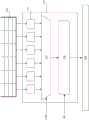
图1A为根据本发明一实施例的光学触控系统100简化后的功能方块图。如图1A所示,光学触控系统100包含一触控面板110、一选择电路120、一读取电路130、一外部处理电路140和一背光模块150。触控面板110包含有多个图像检测单元160,多个图像检测单元160排列成多行和多列的一阵列形状,且选择电路120和读取电路130耦接于每个图像检测单元160。其中,选择电路120和读取电路130设置于触控面板110的一表面上,背光模块150则设置于触控面板110的另一表面,且读取电路130耦接于外部处理电路140。为使图面简洁而易于说明,光学触控系统100中的其他元件与连接关系并未于图1A中示出。FIG. 1A is a simplified functional block diagram of an
于本实施例中,外部处理电路140是设置于一额外的电路板,且触控面板110为玻璃基板,但本发明不以此为限。例如,外部处理电路140亦可设置于触控面板110,而触控面板110亦可为柔性基板。In this embodiment, the
背光模块150用于输出波长位于特定波段内的特定光线(以下简称特定光线),且该特定光线会穿透触控面板110。图像检测单元160用于检测反射入触控面板110的特定光线,并依据检测到的特定光线的强度产生一对应的图像传感值。The
实作上,前述的特定光线可以是红外光波段的光线。In practice, the aforementioned specific light may be light in the infrared light band.
具体而言,图像传感值代表图像检测单元160的一存储电容(图中未示出)所存储的电荷量。当图像检测单元160检测到特定光线时,图像检测单元160会将存储电容放电。并且,图像检测单元160检测到的特定光线的强度越强,图像检测单元160将存储电容放电的速度也越快。如此一来,图像检测单元160便能利用其存储电容存储的电荷量,记录检测到的特定光线的强度。Specifically, the image sensing value represents the amount of charge stored in a storage capacitor (not shown in the figure) of the
选择电路120用于依据驱动时钟脉冲信号CKD和驱动使能信号OE来依序驱动图像检测单元160。读取电路130则用于依据读取时钟脉冲信号CKR和读取使能信号RE读取图像检测单元160。其中,当选择电路120驱动某一列的图像检测单元160时,读取电路130会读取该某一列中的图像测单元160。The
图1B为图1A的光学触控系统部分放大后的功能方块图。以下将结合图1A和图1B进一步说明读取电路130的操作。请参照图1B,读取电路130包含多个放大电路132、一多工器134和一运算电路136。多个放大电路132各自耦接于触控面板110的一行图像传感单元160。多工器134的多个输入端各自耦接于一个放大电路132,多工器134的输出端耦接于运算电路136。FIG. 1B is a partially enlarged functional block diagram of the optical touch system in FIG. 1A . The operation of the
当选择电路120驱动某一列的图像检测单元160时,该某一列的每个图像检测单元160会将存储电容耦接至对应的放大电路132。放大电路132会以电荷分享的方式读取图像检测单元160的存储电容中的图像传感值,然后将读取到的图像传感值输出至多工器134。多工器134会依据读取时钟脉冲信号CKR,选择多个放大电路132其中之一所输出的图像传感值输出至运算电路136。亦即,多工器134会依据读取时钟脉冲信号CKR选择位于某一行的图像检测单元160的图像传感值输出至运算电路136。When the
运算电路136会依据读取使能信号RE判断是否对接收到的图像传感值进行处理,以及是否将处理后的图像传感值输出至外部处理电路140。其中,运算电路136对图像传感值进行的处理可以包含模-数转换或信号放大处理等等。而当外部处理电路140接收到经运算电路136处理后的图像传感值时,外部处理电路140会依据接收到的图像传感值运算出对应于触控物体101的图像,以判断触控物体101和触控面板110接触的位置。The
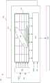
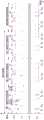
以下将以图2A~图5C进一步说明光学触控系统100的多种操作实施例。图2A为图1A的光学触控系统100的一操作实施例简化后的示意图。如图2A所示,触控面板110上的图像检测单元160排列成包含行K1~K6和列R1~R6的一阵列形状。触控面板110可沿着X-X’直线方向和Y-Y’直线方向划分为一第一触控区域212、一第二触控区域214、一第三触控区域216和一第四触控区域218。其中,第一至第四触控区域212、214、216和218各自包含多个图像检测单元160。于本实施例中,多个图像检测单元160为矩形阵列来排列,但本发明不以此为限,举例而言,多个图像检测单元160亦可呈现相邻两列或两行为错位排列的阵列排列。Various operation embodiments of the
于本实施例中,每个触控区域的多个图像检测单元160包含了三个选定检测单元。其中,选定检测单元代表了读取电路130预定要进行读取的图像检测单元160。详细而言,第一触控区域212的多个图像检测单元160包含了选定检测单元A1、B1和C1。第二触控区域214的多个图像检测单元160包含了选定检测单元A2、B2和C2。第三触控区域216的多个图像检测单元160包含了选定检测单元A3、B3和C3。第四触控区域218的多个图像检测单元160包含了选定检测单元A4、B4和C4。其中,选定检测单元A1、B1、C1、A3、B3和C3位于行K1上,选定检测单元A2、B2、C2、A4、B4和C4则位于行K4上。亦即,同一个触控区域中的选定检测单元位于同一直行。In this embodiment, the plurality of
请注意,本发明中的图像检测单元160以及选定检测单元的数量只是示范性的实施例,并非有意将图像检测单元160和选定检测单元局限在特定数目。并且,触控面板110上的触控区域的数量和每个触控区域所包含的图像检测单元160的数量,亦不以本发明为限。Please note that the number of
图2B为图2A的操作实施例简化后的时序图。如图2B所示,驱动时钟脉冲信号CKD包含多个驱动周期和多个非驱动周期。其中,每个驱动周期具有一第一时间长度T1,每个非驱动周期具有一第二时间长度T2,且第一时间长度T1大于第二时间长度T2。驱动使能信号OE包含了多个驱动使能期间和多个休息期间。其中,处于驱动使能期间的驱动使能信号OE为高电压电平,处于休息期间的驱动使能信号OE为低电压电平。FIG. 2B is a simplified timing diagram of the operational embodiment of FIG. 2A. As shown in FIG. 2B , the driving clock pulse signal CKD includes a plurality of driving periods and a plurality of non-driving periods. Wherein, each driving cycle has a first time length T1, each non-driving cycle has a second time length T2, and the first time length T1 is greater than the second time length T2. The drive enable signal OE includes multiple drive enable periods and multiple rest periods. Wherein, the drive enable signal OE during the drive enable period is at a high voltage level, and the drive enable signal OE during the rest period is at a low voltage level.
当驱动使能信号OE处于高电压电平的驱动使能期间时,驱动时钟脉冲信号CKD会处于第一时间长度T1的驱动周期中。而当驱动使能信号OE处于低电压电平的休息期间时,驱动时钟脉冲信号CKD会处于第二时间长度T2的非驱动周期中。其中,当驱动时钟脉冲信号CKD的驱动周期和驱动使能信号OE的驱动使能期间在时序上重叠时,选择电路120才会驱动图像检测单元160。于图2B的实施例中,依据驱动时钟脉冲信号CKD与驱动使能信号OE来看,于第一触控传感帧频中,选择电路120系为驱动列R1与列R4,而于第二触控传感帧频中,选择电路120则驱动列R2与列R5,于第三触控传感帧频中,选择电路120为驱动列R3与列R6。之后,第四触控传感帧频的操作又回到第一触控传感帧频的操作,而以此为循环周期,在此就不进行赘述。When the driving enable signal OE is in the driving enabling period of the high voltage level, the driving clock pulse signal CKD is in the driving period of the first time length T1. And when the driving enable signal OE is in the rest period of the low voltage level, the driving clock pulse signal CKD is in the non-driving period of the second time length T2. The
在本实施例中,利用驱动时钟脉冲信号CKD、驱动使能信号OE、读取使能信号RE和读取时钟脉冲信号CKR的互相配合,可使读取电路130读取特定的图像检测单元160。请同时参照第2A和2B图,在本实施例的第一触控传感帧频中,当驱动时钟脉冲信号CKD的驱动周期和驱动使能信号OE的驱动使能期间第一次在时序上重叠时,选择电路120会驱动列R1。读取使能信号RE则会于选择电路130的多工器134选择行K1和K4时处于高电位,并于多工器134选择其他行时处于低电位。因此,读取电路130的运算电路136会对列R1中分别位于行K1和行K4的选定检测单元A1和A2的图像传感值进行处理(亦即,读取电路130会读取选定检测单元A1和A2)。In this embodiment, the
换言之,于这段期间中,对应于列R1与行K1之选定检测单元A1以及对应于列R1与行K4之选定检测单元A2会进行感应与读取。因此,第一触控区域212之选定检测单元A1与第二触控区域214之选定检测单元A2会被依序驱动进行感应,且依序进行读取感应值。In other words, during this period, the selected detection unit A1 corresponding to the column R1 and the row K1 and the selected detection unit A2 corresponding to the column R1 and the row K4 perform sensing and reading. Therefore, the selected detection unit A1 of the
同样于第一触控传感帧频中,当驱动时钟脉冲信号CKD的驱动周期和驱动使能信号OE的驱动使能期间第二次在时序上重叠时,选择电路120会驱动列R4,读取使能信号RE则会于多工器134选择行K1和K4时处于高电位,并于多工器134选择其他行时处于低电位。因此,读取电路130会读取列R4中分别位于行K1和行K4的选定检测单元A3和A4。Also in the first touch sensing frame rate, when the driving period of the driving clock pulse signal CKD and the driving enabling period of the driving enabling signal OE overlap in timing for the second time, the
换言之,于这段期间中,对应于列R4与行K1之选定检测单元A3以及对应于列R4与行K4之选定检测单元A4会进行感应与读取。因此,第三触控区域216之选定检测单元A3与第四触控区域218之选定检测单元A4会被依序驱动进行感应,且依序进行读取感应值。因此,于本实施例之第一触控传感帧频中,每一触控区域中分别针对单一个选定检测单元进行感应与读取,举例而言,于第一触控传感帧频期间,传感与读取的顺序为第一触控区域212之选定检测单元A1、第二触控区域214之选定检测单元A2、第三触控区域216之选定检测单元A3与第四触控区域218之选定检测单元A4。In other words, during this period, the selected detection unit A3 corresponding to the column R4 and the row K1 and the selected detection unit A4 corresponding to the column R4 and the row K4 perform sensing and reading. Therefore, the selected detection unit A3 of the
在本实施例的第二触控传感帧频中,选择电路120改为驱动列R2和列R5中的图像检测单元160。当选择电路120驱动列R2时,读取电路130会读取列R2中分别位于行K1和行K4的选定检测单元B1和B2。当选择电路120驱动列R5时,读取电路130会读取列R5中分别位于行K1和行K4的选定检测单元B3和B4。具体而言,于第二触传感帧频中,每一触控区域中分别针对单一个选定检测单元进行感应与读取。请参阅图2A与图2B,于第二触控传感帧频期间,传感与读取的顺序为第一触控区域212之选定检测单元B1、第二触控区域214之选定检测单元B2、第三触控区域216之选定检测单元B3与第四触控区域218之选定检测单元B4。In the second touch sensing frame rate of this embodiment, the
在本实施例的第三触控传感帧频中,选择电路120改为驱动列R3和R6中的图像检测单元160。当选择电路120驱动列R3时,读取电路130会读取列R3中分别位于行K1和行K4的选定检测单元C1和C2。当选择电路120驱动列R6时,读取电路130会读取列R6中分别位于行K1和行K4的选定检测单元C3和C4。具体而言,于第三触传感帧频中,每一触控区域中分别针对单一个选定检测单元进行感应与读取。请参阅图2A与图2B,于第三触控传感帧频期间,传感与读取的顺序为第一触控区域212之选定检测单元C1、第二触控区域214之选定检测单元C2、第三触控区域216之选定检测单元C3与第四触控区域218之选定检测单元C4。In the third touch sensing frame rate of this embodiment, the
在本实施例的第四触控传感帧频中,选择电路120和读取电路130的配合操作,相似于第一触控传感帧频中两者的配合操作,为简洁起见,在此不重复赘述。In the fourth touch sensing frame rate of this embodiment, the cooperative operation of the
换言之,如图2B所示,选择电路120和读取电路130的配合操作是以三个触控传感帧频为一循环周期。例如,第一至第三触控传感帧频属于同一个循环周期,而第四触控传感帧频则为另一个循环周期的第一个触控传感帧频。因此,驱动时钟脉冲信号CKD和驱动使能信号OE的波形在相邻的触控传感帧频中不相同。In other words, as shown in FIG. 2B , the cooperative operation of the selecting
于本实施例中,读取电路130会在每个触控传感帧频中,将读取到的图像传感值传送给外部处理电路140。外部处理电路140则会于每个触控传感帧频中,依据接收到的图像传感值计算出对应于触控物体101的图像。In this embodiment, the
由上述可知,于图2A与图2B之实施例中,触控面板110可形成多个触控区域,如第一触控区域212、第二触控区域214、第三触控区域216与第四触控区域218。每一个触控区域中,可于多个图像检测单元160中挑选出一或多个选定检测单元(例如,三个选定检测单元),并且选定检测单元会被依序驱动进行触控感应与读取感应值。于本实施例中,每一触控区域之选定检测单元为纵向排列(如图2A所示),可视为进行纵向读取的方式。并且,于时序相邻的两个触控传感帧频中,读取电路130不会读取相同的选定检测单元。因此,光学触控系统100可以确保每个选定检测单元皆有充裕的时间依据检测到的特定光线强度将存储电容放电,进而可以增进图像传感的精确度。As can be seen from the above, in the embodiment of FIG. 2A and FIG. 2B , the
如前所述,读取电路130是利用放大电路132以电荷分享的方式读取图像检测单元160中的图像传感值。为了使放大电路132能有更充裕的时间进行电荷分享,当选择电路120驱动某一列的图像检测单元160时,读取电路130可以等待预定时间后才读取该某一列的图像检测单元160,而不会立即读取该某一列的图像检测单元160。如此一来,便能进一步提升读取电路130读取到的图像传感值的精确度。As mentioned above, the
例如,在某些实施例中,光学触控系统100的操作方式如图2A和图2C所示。于第一触控传感帧频中,当选择电路120驱动列R1时,读取使能信号RE会于预定时间Tx中先处于低电位,以使分别对应列K1~K6的多个放大电路132能有充分的时间进行电荷分享,然后读取使能信号RE才于多工器134选择列K1和K4时切换为高电位,以使读取电路130读取选定检测单元A1和A2。于之后的触控测帧频中,当选择电路120驱动某一列时,读取使能信号RE同样会先于预定时间Tx中处于低电位,然后才切换为高电位,使读取电路130读取该某一列包含的选定检测单元,为简洁起见,在此不重复赘述。For example, in some embodiments, the
另外,预定时间Tx的长度可依据所需图像精确度的不同而整。因此,当驱动使能信号OE处于驱动使能期间或休息期间时,读取电路130皆可读取选定检测单元。亦即,当驱动使能信号OE处于驱动使能期间或休息期间时,读取使能信号RE会一或多次切换电压电平。In addition, the length of the predetermined time Tx can be adjusted according to the required image accuracy. Therefore, when the driving enable signal OE is in the driving enable period or in the rest period, the
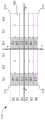
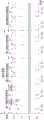
图3A为图1A的光学触控系统100的另一操作实施例简化后的示意图。图3A的实施例和图2A的实施例相似,差异在于图3A的选定检测单元的位置,不同于图2A的选定检测单元的位置。具体而言,于图3A的实施例中,选定检测单元A1、B1、C1位于第一触控区域212的对角线上。选定检测单元A2、B2、C2位于第二触控区域214的对角线上。选定检测单元A3、B3、C3位于第三触控区域216的对角线上。选定检测单元A4、B4、C4位于第四触控区域218的对角线上。亦即,每个触控区域中的选定检测单元位于该触控区域的对角线上。FIG. 3A is a simplified schematic diagram of another operation embodiment of the
图3B为图3A的操作实施例简化后的时序图。请同时参照第3A和图3B,在本实施例的第一触控传感帧频中,当选择电路120驱动列R1或列R4中的图像检测单元160时,读取使能信号RE会于多工器134选择行K1和K4时处于高电位,并于多工器134选择其他行时处于低电位。因此,在第一触控传感帧频中,读取电路130会读取列R1中分别位于行K1和行K4的选定检测单元A1和A2,以及读取列R4中分别位于行K1和行K4的选定检测单元A3和A4。FIG. 3B is a simplified timing diagram of the operational embodiment of FIG. 3A. Please refer to FIG. 3A and FIG. 3B at the same time. In the first touch sensing frame rate of this embodiment, when the
在本实施例的第二触控传感帧频中,当选择电路120驱动列R2或列R5中的图像检测单元160时,读取使能信号RE会于多工器134选择行K2和K5时处于高电位,并于多工器134选择其他行时处于低电位。因此,在第二触控传感帧频中,读取电路130会读取列R2中分别位于行K2和行K5的选定检测单元B1和B2,以及读取列R5中分别位于行K2和行K5的选定检测单元B3和B4。In the second touch sensing frame rate of this embodiment, when the
在本实施例的第三触控传感帧频中,当选择电路120驱动列R3或列R6中的图像检测单元160时,读取使能信号RE会于多工器134选择行K3和K6时处于高电位,并于多工器134选择其他行时处于低电位。因此,在第三触控传感帧频中,读取电路130会读取列R3中分别位于行K3和行K6的选定检测单元C1和C2,以及读取列R6中分别位于行K3和行K6的选定检测单元C3和C4。In the third touch sensing frame rate of this embodiment, when the
在本实施例的第四触控传感帧频中,选择电路120和读取电路130的操作,相似于第一触控传感帧频中两者的配合操作,为简洁起见,在此不重复赘述。于图3A与图3B实施例中,每一触控传感区域的选定检测单元为对角线排列,可视为进行斜向读取的方式。In the fourth touch sensing frame rate of this embodiment, the operations of the
换言之,在本实施例中,选择电路120和读取电路130的配合操作,是以三个触控传感帧频为一循环周期。因此,驱动时钟脉冲信号CKD和驱动使能信号OE的波形在相邻的触控传感帧频中不相同。In other words, in this embodiment, the cooperative operation of the selecting
第2A~2B图的实施例中的许多功能方块的操作方式以及优点,同样适用于第3A~3B图的实施例。另外,第3A~3B图的实施例也可以采用类似图2C的实施例的操作方式。亦即,可将图3B中的读取使能信号RE延迟预定时间Tx,为简洁起见,在此不重复赘述。The operation methods and advantages of many functional blocks in the embodiments of Figs. 2A-2B are also applicable to the embodiments of Figs. 3A-3B. In addition, the embodiment in FIGS. 3A-3B can also adopt an operation mode similar to the embodiment in FIG. 2C . That is, the read enable signal RE in FIG. 3B may be delayed by a predetermined time Tx, and for the sake of brevity, details are not repeated here.
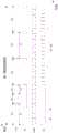
图4A为图1A的光学触控系统100的再一操作实施例简化后的示意图。图4A的实施例和图2A的实施例相似,差异在于图4A的选定检测单元的位置,不同于图2A的选定检测单元的位置。具体而言,第一触控区域212的选定检测单元A1、B1和C1以及第二触控区域214的选定检测单元A2、B2和C2位于列R1上,第三触控区域216的选定检测单元A3、B3和C3以及第四触控区域218的选定检测单元A4、B4和C4位于列R4上。亦即,每个触控区域中的选定检测单元位于同一横列。FIG. 4A is a simplified schematic diagram of still another operation embodiment of the
图4B为图4A的操作实施例简化后的时序图。请同时参照第4A和图4B,本实施例的选择电路120在每个触控传感帧频中,只会驱动列R1和R4中的图像检测单元160。FIG. 4B is a simplified timing diagram of the operational embodiment of FIG. 4A. Please refer to FIG. 4A and FIG. 4B at the same time, the
在本实施例的一第一触控传感帧频中,当选择电路120驱动列R1中的图像检测单元160时,读取电路130会读取列R1中分别位于行K1和K4的选定检测单元A1和A2。当选择电路120驱动列R4中的图像检测单元160时,读取电路130会读取列R4中分别位于行K1和K4的选定检测单元A3和A4。In a first touch sensing frame rate of this embodiment, when the
在本实施例的一第二触控传感帧频中,当选择电路120驱动列R1中的图像检测单元160时,读取电路130会读取列R1中分别位于行K2和K5的选定检测单元B1和B2。当选择电路120驱动列R4中的图像检测单元160时,读取电路130会读取列R4中分别位于行K2和K5的选定检测单元B3和B4。In a second touch sensing frame rate of this embodiment, when the
在本实施例的一第三触控传感帧频中,当选择电路120驱动列R1中的图像检测单元160时,读取电路130会读取列R1中分别位于行K3和K6的选定检测单元C1和C2。当选择电路120驱动列R4中的图像检测单元160时,读取电路130会读取列R4中分别位于行K3和K6的选定检测单元C3和C4。In a third touch sensing frame rate of this embodiment, when the
在本实施例的一第四触控传感帧频中,选择电路120和读取电路130的配合操作,相似于第一触控传感帧频中两者的配合操作,为简洁起见,在此不重复赘述。于图4A与图4B实施例中,每一触控传感区域的检测单元为横向排列,可视为进行横向读取的方式。In the fourth touch sensing frame rate of this embodiment, the cooperative operation of the
在本实施例中,选择电路120和读取电路130的配合操作是以三个触控传感帧频为一循环周期。值得注意的是,选择电路120的操作则是以一个触控传感帧频为一周期。因此,驱动时钟脉冲信号CKD和驱动使能信号OE的波形在相邻的触控传感帧频中相同。In this embodiment, the cooperative operation of the selecting
第2A~2B图的实施例中的许多功能方块的操作方式以及优点,同样适用于第4A~4B图的实施例。另外,第4A~4B图的实施例也可以采用类似图2C的实施例的操作方式。亦即,可将图4B中的读取使能信号RE延迟预定时间Tx,为简洁起见,在此不重复赘述。The operation modes and advantages of many functional blocks in the embodiments of Figs. 2A-2B are also applicable to the embodiments of Figs. 4A-4B. In addition, the embodiment in FIGS. 4A-4B can also adopt an operation mode similar to the embodiment in FIG. 2C . That is, the read enable signal RE in FIG. 4B may be delayed by a predetermined time Tx, and for the sake of brevity, details are not repeated here.
在上述的多个实施例中,于每个触控传感帧频中,选择电路120只会驱动每一个触控区域中的一列图像检测单元160。实作上,于每个触控传感帧频中,选择电路120可以改为驱动每个触控区域中相邻的多列图像检测单元160,以提升读取电路130的读取结果的正确率。In the above-mentioned multiple embodiments, in each touch sensing frame rate, the
例如,在某一实施例中,当读取电路130于某一触控传感帧频中欲读取位于列R2的选定检测单元时,选择电路120可先驱动列R1中的图像检测单元160。如此一来,与列R2的选定检测单元位于同一行的列R1的一特定图像检测单元,便会将存储电容中的电荷分享至列R2的选定检测单元所对应的放大电路132。接着,选择电路120才会驱动列R2,以使列R2的选定检测单元将存储电容中的电荷分享至对应的放大电路132。如此一来,当读取电路130读取列R2的选定检测单元时,除了会读取到来自列R2的选定检测单元的电荷,还会一并读取到来自列R1的特定图像检测单元的电荷。因此,读取电路130所读取到的电荷量会增加,进而提升了读取电路130的读取结果的正确率。For example, in one embodiment, when the
在上述的多个实施例中,读取电路130在相邻的触控传感帧频中,不会读取相同的选定检测单元。如此一来,光学触控系统100便可确保每个选定检测单元皆有充裕的时间针对特定光线进行传感。In the above-mentioned multiple embodiments, the
另外,因为驱动时钟脉冲信号CKD的驱动周期的时间长度(第一时间长度T1),大于非驱动周期的时间长度(第二时间长度T2),所以光学触控系统100可确保读取电路130于每个触控传感帧频中,皆有充分的时间进行读取。In addition, because the time length of the driving period (the first time length T1) of the driving clock pulse signal CKD is greater than the time length of the non-driving period (the second time length T2), the
图5A为图1A的光学触控系统100的再一操作实施例简化后的示意图。如图5A所示,触控面板110上的图像检测单元160排列成多行K1~K6和多列R1~R6的一阵列形状。触控面板110可沿着X-X’直线方向和Y-Y’直线方向划分为一第一触控区域512、一第二触控区域514、一第三触控区域516和一第四触控区域518。其中,第一至第四触控区域512、514、516和518各自包含多个图像检测单元160。FIG. 5A is a simplified schematic diagram of still another operation embodiment of the
第一触控区域512的多个图像检测单元160包含了选定检测单元A1、B1和C1,且选定检测单元A1、B1和C1位于第一触控区域512的对角线上。第二触控区域514的多个图像检测单元包含了选定检测单元A2、B2和C2,且选定检测单元A2、B2和C2位于第二触控区域514的对角线上。第三触控区域516和第四触控区域518的多个图像检测单元160则包含了选定检测单元M1~M18。亦即,第三触控区域516和第四触控区域518的图像检测单元160全部都是选定检测单元。The multiple
图5B为图5A的操作实施例简化后的时序图。请同时参照第5A和图5B,在本实施例中,驱动时钟脉冲信号CKD包含多个驱动周期、多个非驱动周期和多个延长驱动周期。驱动周期具有一第一时间长度T1,非驱动周期具有一第二时间长度T2,而延长驱动周期则具有一第三时间长度T3。其中,第一时间长度T1大于第二时间长度T2,第三时间长度T3则大于第一时间长度T1。FIG. 5B is a simplified timing diagram of the operational embodiment of FIG. 5A. Please refer to FIG. 5A and FIG. 5B at the same time. In this embodiment, the driving clock pulse signal CKD includes a plurality of driving periods, a plurality of non-driving periods and a plurality of extended driving periods. The driving period has a first time length T1, the non-driving period has a second time length T2, and the extended driving period has a third time length T3. Wherein, the first time length T1 is longer than the second time length T2, and the third time length T3 is longer than the first time length T1.
驱动使能信号OE包含一驱动使能期间和一休息期间。其中处于驱动使能期间的驱动使能信号OE为高电压电平,处于休息期间的驱动使能信号OE为低电压电平。The drive enable signal OE includes a drive enable period and a rest period. The drive enable signal OE during the drive enable period is at a high voltage level, and the drive enable signal OE during the rest period is at a low voltage level.
当驱动使能信号OE处于高电压电平的驱动使能期间时,驱动时钟脉冲信号CKD会处于第一时间长度T1的驱动周期中,或是处于第三时间长度T3的延长驱动周期中。当驱动使能信号OE处于低电压电平的休息期间时,驱动时钟脉冲信号CKD会处于第二时间长度T2的非驱动周期中。其中,当驱动时钟脉冲信号CKD的驱动周期或延长驱动周期,与驱动使能信号OE的驱动使能期间于时序上重叠时,选择电路120才会驱动图像检测单元160。When the driving enable signal OE is in the driving enable period of the high voltage level, the driving clock signal CKD is in the driving period of the first time length T1 or in the extended driving period of the third time length T3 . When the driving enable signal OE is in the rest period of the low voltage level, the driving clock pulse signal CKD is in the non-driving period of the second time length T2. The
图5C为图5B部分放大后的时序图。如图5C所示,本实施例的读取时钟脉冲信号CKR和读取使能信号RE与驱动使能信号OE之间的时序变化关系,相似于第2A~2B图的实施例,为简洁起见,在此不重复赘述。FIG. 5C is a partially enlarged timing diagram of FIG. 5B . As shown in FIG. 5C, the timing variation relationship between the read clock pulse signal CKR, the read enable signal RE, and the drive enable signal OE in this embodiment is similar to the embodiment in FIGS. 2A-2B, for the sake of brevity. , which will not be repeated here.
请同时参照第5A~5C图,在本实施例的第一触控传感帧频中,选择电路120会驱动列R1和R4~R6。当选择电路120驱动列R1时,读取使能信号RE会于多工器134选择行K1和K4时处于高电位,并于多工器134选择其他行时处于低电位。因此,读取电路130会依序读取列R1中的选定检测单元A1和A2。当选择电路120驱动列R4~R6时,读取使能信号RE则会于多工器134选择行K1~K6时都处于高电位。因此,读取电路130会依序读取列R4~R6中的选定检测单元M1~M18。Please refer to FIGS. 5A-5C at the same time. In the first touch-sensing frame rate of this embodiment, the
在本实施例的第二触控传感帧频中,选择电路120会驱动列R2和R4~R6。当选择电路120驱动列R2时,读取使能信号RE会于多工器134选择行K2和K5时处于高电位,并于多工器134选择其他行时处于低电位。因此,读取电路130会依序读取列R2中的选定检测单元B1和B2。当选择电路120驱动列R4~R6时,读取使能信号RE则会于多工器134选择行K1~K6时都处于高电位。因此,读取电路130会依序读取列R4~R6中的选定检测单元M1~M18。In the second touch sensing frame rate of this embodiment, the
在本实施例的第三触控传感帧频中,选择电路120会驱动列R3和R4~R6。当选择电路120驱动列R3时,读取使能信号RE会于多工器134选择行K3和K6时处于高电位,并于多工器134选择其他行时处于低电位。因此,读取电路130会依序读取列R3中的选定检测单元C1和C2。当选择电路120驱动列R4~R6时,读取使能信号RE则会于多工器134选择行K1~K6时都处于高电位。因此,读取电路130会依序读取列R4~R6中的选定检测单元M1~M18。In the third touch-sensing frame rate of this embodiment, the
在本实施例的第四触控传感帧频中,选择电路120和读取电路130的配合操作,相似于第一触控传感帧频中两者的配合操作,为简洁起见,在此不再赘述。In the fourth touch sensing frame rate of this embodiment, the cooperative operation of the
由上述可知,在每个触控传感帧频中,读取电路130都会读取第三触控区域516和第四触控区域518中的所有的图像检测单元160(亦即,选定检测单元M1~M18)。因此,当外部处理电路140在计算触控物体101的图像时,由第三触控区域516和第四触控区域518的多个图像传感值所计算出的图像的解析度,会高于由第一触控区域512和第二触控区域514的多个图像传感值所计算出的图像的解析度。It can be known from the above that, in each touch sensing frame rate, the
另外,由于驱动时钟脉冲信号CKD的延长驱动周期的时间长度(第三时间长度T3),大于驱动周期的时间长度(第一时间长度T1),所以读取电路130有充裕的时间读取第三触控区域516和第四触控区域518的图像检测单元160。如此一来,可以进一步提高由第三触控区域516和第四触控区域518的多个图像传感值所计算出的图像的清晰度。In addition, since the time length of the extended driving cycle (the third time length T3) of the driving clock pulse signal CKD is greater than the time length of the driving cycle (the first time length T1), the
实作上,第三触控区域516和第四触控区域518可用于指纹辨识的相关应用。另外,在对图像清晰度无特别要求的某些实施例中,第三时间长度T3也可设置为等于第一时间长度T1。In practice, the
很明显地,第5A~5C图的实施例中的第一触控区域512和第二触控区域514的操作方式,相似于第3A~3B图的实施例的操作方式。实作上,也可将第5A~5C图的实施例中的第一触控区域512和第二触控区域514的操作方式,设置为相似于第2A~2B图或第4A~4B图的实施例的操作方式。Obviously, the operation modes of the
图6A为依据本发明另一实施例的光学触控系统600的一操作实施例简化后的示意图。如图6A所示,光学触控系统600包含一触控面板610,触控面板610包含多个图像检测单元160。触控面板610可沿着X-X’直线和Y-Y’直线划分为一第一触控区域612、一第二触控区域614、一第三触控区域616和一第四触控区域618。其中,第一至第四触控区域612、614、616和618各自包含多个图像检测单元160。光学触控系统100的许多功能方块的操作方式及优点,同样适用于光学触控系统600,为简洁起见,在此不重复赘述。并且,为使图面简洁而易于说明,光学触控系统600中的其他元件与连接关系并未绘示于第6图中。FIG. 6A is a simplified schematic diagram of an operation embodiment of an
光学触控系统600的操作方式可设置为相似于前述第3A~3B图的实施例的操作方式。亦即,光学触控系统600会于每个触控传感帧频中,读取每个触控区域中的一个图像检测单元。并且,光学触控系统600会以虚线所示方向,依序读取每个触控区域的对角线上的触控检测单元160。The operation mode of the
在本实施例中,触控物体101接触于第一触控区域612,且没有接触于第二、第三和第四触控区域614、616和618。触控物体101于触控面板110上的一投影603覆盖了第二触控区域614。因此,第一触控区域612和第二触控区域614皆会接收到由触控物体101所反射的特定光线。In this embodiment, the
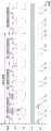
图6B为光学触控系统600于连续的多个的触控传感帧频中对图6A的图像检测单元160进行读取后所得的图像传感值的时序变化图。点A~F分别代表光学触控系统600于六个触控传感帧频中所读取到的不同位置的图像传感值的大小。如图6B所示,由于触控物体101接触于第一触控区域612,所以第一触控区域612的多个图像传感值的大小,会对应于触控物体101的表面纹路(例如,手指的指纹)而呈现反复变化。FIG. 6B is a time-series change diagram of image sensing values obtained after the
由于第二触控区域614的部分区域被投影603所覆盖,其余区域则未被投影603所覆盖。所以第二触控区域614的多个图像传感值的大小,会呈现一具有较低数值的群组(亦即,点A~D),以及另一具有较高数值的群组(亦即,点E~F)。其中具有较低数值的群组对应于被投影603所覆盖的部分区域,具有较高数值的群组对应于未被投影603所覆盖的其余区域,且两个群组的边界对应于投影603的边界。Since a part of the
由于第三和第四触控区域616和618没有和触控物体101接触,也没有被投影区域603所覆盖,所以第三和第四触控区域616和618的多个图像传感值的大小,会彼此接近且具有一较高数值。Since the third and
光学触控系统600可依据不同位置的图像传感值的大小的变化方式,判断触控物体101所接触的触控区域。在本实施例中,因为第一触控区域612的多个图像传感值的大小呈现周期性的反复变化,即如图6B之触控区域612呈现有波峰波谷的传感值变化,光学触控系统600会判定触控物体101接触于第一触控区域612。The
另一方面,因为第二、第三和第四触控区域614、616和618的多个图像传感值的大小没有呈现周期性的反复变化,所以光学触控系统600会判定触控物体101没有接触于第二、第三和第四触控区域614、616和618。On the other hand, because the magnitudes of the multiple image sensing values of the second, third and
由上述可知,光学触控系统600可以有效降低因阴影遮蔽而产生误动作的机率。From the above, it can be seen that the
图7是根据本发明另一实施例的光学触控系统700简化后的功能方块图。光学触控系统700相似于光学触控系统100,亦即光学触控系统700适用第2A~4B图的操作方式。光学触控系统700和光学触控系统100的差异在于,光学触控系统700以显示器模块710替代光学触控系统100中的背光模块150。为使图面简洁而易于说明,光学触控系统700中的其他元件与连接关系并未绘示于图7中。FIG. 7 is a simplified functional block diagram of an
光学触控系统700的显示器模块710包含一栅极驱动电路720、一源极驱动电路730、多个栅极信号线740、多个源极信号线750和一像素区760。其中,多个栅极信号线740和多个源极信号线750分别耦接于像素区760触控面板110可藉由合适的黏着剂直接胶合于显示器模块710,或是藉由合适的固定结构栓锁于显示器模块710的边框,但本发明不以此为限。The
与光学触控系统100相似,光学触控系统700的触控面板110的多个图像检测单元160排列成包含行K1~K6和列R1~R6的一阵列形状,且光学触控系统700的触控面板110可划分为多个触控区域。其中,多个触控区域与像素区760在垂直投影方向上重叠。Similar to the
在某些实施例中,光学触控系统700只有部分触控区域和像素区760在垂直投影方向上重叠。In some embodiments, only part of the touch area of the
于图7的实施例中,触控面板110的多个图像检测单元160会重叠于栅极信号线740或源极信号线750。为避免栅极信号线740或源极信号线750上的信号透过电容耦合干扰触控面板110的操作,光学触控系统700可采用相似于第2A~2B图、第3A~3B图或第4A~4B图的实施例中的操作方式。In the embodiment of FIG. 7 , a plurality of
例如,在光学触控系统700采用相似于第2A~2B图的纵向读取方式的情况下,当栅极驱动电路720利用与行K2重叠的栅极信号线740传送信号时,光学触控系统700可读取位于行K1的选定检测单元。For example, in the case where the
又例如,在光学触控系统700采用相似于第4A~4B图的横向读取方式的情况下,当源极驱动电路730利用与列R2重叠的源极信号线750传送信号时,光学触控系统700可读取位于列R1的选定检测单元。For another example, in the case where the
又例如,在光学触控系统700采用相似于第3A~3B图的斜向读取方式的情况下,当栅极驱动电路720利用与行K2重叠的栅极信号线740传送信号,且源极驱动电路730利用与列R2重叠的源极信号线750传送信号时,光学触控系统700可读取位于行K1和列R1交会处的选定检测单元。当栅极驱动电路720利用与行K3重叠的栅极信号线740传送信号,且源极驱动电路730利用与列R3重叠的源极信号线750传送信号时,光学触控系统700可读取位于行K2和列R2交会处的选定检测单元。亦即,多个选定检测单元的排列方向,与栅极信号线740或源极信号线750的延伸方向不相同。For another example, in the case that the
由上述可知,若某一图像传感单元160与正在传输信号的栅极信号线740或源极信号线750重叠,光学触控系统700不会读取该图像传感单元160。因此,光学触控系统700可有效避免显示器模块710干扰触控面板110的操作,使得光学触控系统700适用于于智能手机或平板电脑等需要结合触控面板与显示器模块的电子产品。It can be seen from the above that if an
实作上,光学触控系统100和700还可将不同触控区域的图像拼接,以进行安全验证相关判断。例如,在某些实施例中,当使用者的手指于光学触控系统100或700的触控面板110上移动时,光学触控系统100或700会将不同触控区域的图像拼接,以得到使用者的指纹图像。接着,光学触控系统100或700会依据指纹图像辨识使用者身分,以决定是否回应使用者的操作输入。In practice, the
于上述实施例的图示与说明中,为便于清楚图示来表达内容,其触控面板之图像检测单元160仅以列R1~R6与行K1~K6来说明,但本发明不以此为限。In the illustrations and descriptions of the above-mentioned embodiments, in order to express the content clearly, the
在说明书及申请专利范围中使用了某些词汇来指称特定的元件。然而,所属技术领域中具有通常知识者应可理解,同样的元件可能会用不同的名词来称呼。说明书及申请专利范围并不以名称的差异做为区分元件的方式,而是以元件在功能上的差异来做为区分的基准。在说明书及申请专利范围所提及的「包含」为开放式的用语,故应解释成「包含但不限定于」。另外,「耦接」在此包含任何直接及间接的连接手段。因此,若文中描述第一元件耦接于第二元件,则代表第一元件可通过电性连接或无线传输、光学传输等信号连接方式而直接地连接于第二元件,或者通过其他元件或连接手段间接地电性或信号连接至该第二元件。Certain terms are used in the specification and claims to refer to particular elements. However, those skilled in the art should understand that the same element may be called by different terms. The description and the scope of the patent application do not use the difference in the name as the way to distinguish the components, but the difference in the function of the components as the basis for the distinction. The term "comprising" mentioned in the specification and scope of patent application is an open term, so it should be interpreted as "including but not limited to". In addition, "coupling" here includes any direct and indirect connection means. Therefore, if it is described that the first element is coupled to the second element, it means that the first element can be directly connected to the second element through electrical connection or signal connection means such as wireless transmission or optical transmission, or through other elements or connections. The means are indirectly electrically or signally connected to the second element.
当然,本发明还可有其它多种实施例,在不背离本发明精神及其实质的情况下,熟悉本领域的技术人员当可根据本发明作出各种相应的改变和变形,但这些相应的改变和变形都应属于本发明所附的权利要求的保护范围。Certainly, the present invention also can have other multiple embodiments, without departing from the spirit and essence of the present invention, those skilled in the art can make various corresponding changes and deformations according to the present invention, but these corresponding Changes and deformations should belong to the scope of protection of the appended claims of the present invention.
Claims (5)
Translated fromChinesePriority Applications (1)
| Application Number | Priority Date | Filing Date | Title |
|---|---|---|---|
| CN202011284035.4ACN112527142B (en) | 2017-12-19 | 2018-02-05 | Optical touch system |
Applications Claiming Priority (4)
| Application Number | Priority Date | Filing Date | Title |
|---|---|---|---|
| TW106144632 | 2017-12-19 | ||
| TW106144632ATWI658393B (en) | 2017-12-19 | 2017-12-19 | Optical touch system |
| CN201810114900.7ACN108319393B (en) | 2017-12-19 | 2018-02-05 | Optical touch system |
| CN202011284035.4ACN112527142B (en) | 2017-12-19 | 2018-02-05 | Optical touch system |
Related Parent Applications (1)
| Application Number | Title | Priority Date | Filing Date |
|---|---|---|---|
| CN201810114900.7ADivisionCN108319393B (en) | 2017-12-19 | 2018-02-05 | Optical touch system |
Publications (2)
| Publication Number | Publication Date |
|---|---|
| CN112527142A CN112527142A (en) | 2021-03-19 |
| CN112527142Btrue CN112527142B (en) | 2023-04-11 |
Family
ID=62902552
Family Applications (2)
| Application Number | Title | Priority Date | Filing Date |
|---|---|---|---|
| CN201810114900.7AActiveCN108319393B (en) | 2017-12-19 | 2018-02-05 | Optical touch system |
| CN202011284035.4AActiveCN112527142B (en) | 2017-12-19 | 2018-02-05 | Optical touch system |
Family Applications Before (1)
| Application Number | Title | Priority Date | Filing Date |
|---|---|---|---|
| CN201810114900.7AActiveCN108319393B (en) | 2017-12-19 | 2018-02-05 | Optical touch system |
Country Status (3)
| Country | Link |
|---|---|
| US (1) | US10664081B2 (en) |
| CN (2) | CN108319393B (en) |
| TW (1) | TWI658393B (en) |
Families Citing this family (1)
| Publication number | Priority date | Publication date | Assignee | Title |
|---|---|---|---|---|
| TWI679431B (en)* | 2018-07-31 | 2019-12-11 | 友達光電股份有限公司 | Fingerprint sensing device and detection method thereof |
Citations (4)
| Publication number | Priority date | Publication date | Assignee | Title |
|---|---|---|---|---|
| CN101354625A (en)* | 2008-09-22 | 2009-01-28 | 友达光电股份有限公司 | Touch display panel, manufacturing method thereof and touch method thereof |
| CN102314247A (en)* | 2010-06-29 | 2012-01-11 | 瀚宇彩晶股份有限公司 | touch panel |
| CN103309519A (en)* | 2013-03-19 | 2013-09-18 | 友达光电股份有限公司 | Touch position detection method and optical touch device using same |
| WO2016144108A1 (en)* | 2015-03-10 | 2016-09-15 | 크루셜텍 (주) | Display device capable of scanning images |
Family Cites Families (33)
| Publication number | Priority date | Publication date | Assignee | Title |
|---|---|---|---|---|
| US7176432B2 (en)* | 2003-06-06 | 2007-02-13 | Seiko Npc Corporation | Image detection processor and image detection processing method |
| US20050219229A1 (en)* | 2004-04-01 | 2005-10-06 | Sony Corporation | Image display device and method of driving image display device |
| TWI469019B (en) | 2009-04-30 | 2015-01-11 | Chimei Innolux Corp | Power saving apparatus for capacitive touch screen and power saving method for same and capacitive touch screen employing power saving apparatus |
| CN101908306B (en)* | 2009-06-02 | 2012-07-04 | 瀚宇彩晶股份有限公司 | Test method and array tester for optical touch panel |
| WO2011040094A1 (en)* | 2009-09-30 | 2011-04-07 | シャープ株式会社 | Display device |
| WO2011040091A1 (en)* | 2009-09-30 | 2011-04-07 | シャープ株式会社 | Display device |
| WO2011040090A1 (en)* | 2009-09-30 | 2011-04-07 | シャープ株式会社 | Display device |
| EP2485127A4 (en)* | 2009-09-30 | 2014-07-30 | Sharp Kk | Display device |
| BR112012007103A2 (en)* | 2009-09-30 | 2016-04-26 | Sharp Kk | display device |
| WO2011065555A1 (en)* | 2009-11-30 | 2011-06-03 | シャープ株式会社 | Display device |
| US20120235967A1 (en)* | 2009-11-30 | 2012-09-20 | Sharp Kabushiki Kaisha | Display device |
| CN102129326B (en)* | 2010-01-19 | 2015-03-25 | 原相科技股份有限公司 | Positioning method of optical touch device and optical touch device |
| WO2011104957A1 (en)* | 2010-02-26 | 2011-09-01 | シャープ株式会社 | Display device |
| WO2011145676A1 (en)* | 2010-05-20 | 2011-11-24 | シャープ株式会社 | Display device with touch sensor |
| WO2011145507A1 (en)* | 2010-05-20 | 2011-11-24 | シャープ株式会社 | Display device |
| WO2011145677A1 (en)* | 2010-05-20 | 2011-11-24 | シャープ株式会社 | Display device equipped with touch sensor |
| WO2012014819A1 (en)* | 2010-07-26 | 2012-02-02 | シャープ株式会社 | Display device |
| US8816285B2 (en)* | 2010-07-26 | 2014-08-26 | Sharp Kabushiki Kaisha | Display device |
| US20130113768A1 (en)* | 2010-07-27 | 2013-05-09 | Sharp Kabushiki Kaisha | Display device and drive method for same |
| WO2012014864A1 (en)* | 2010-07-27 | 2012-02-02 | シャープ株式会社 | Display device |
| CN102446022B (en)* | 2010-10-04 | 2016-01-13 | 剑扬股份有限公司 | touch screen system |
| TWI524239B (en)* | 2010-10-08 | 2016-03-01 | 友達光電股份有限公司 | Method for locating touch position |
| TWI471792B (en) | 2011-03-30 | 2015-02-01 | Edamak Corp | Method for detecting multi-object behavior of a proximity-touch detection device |
| KR101878976B1 (en)* | 2011-07-07 | 2018-07-17 | 삼성디스플레이 주식회사 | Method of driving touch sensing display panel and display apparatus performing the same |
| US8860695B2 (en)* | 2011-08-05 | 2014-10-14 | Pixart Imaging Inc. | Optical touch system and electronic apparatus including the same |
| TWI470509B (en)* | 2011-09-08 | 2015-01-21 | Hannstar Display Corp | Optical touch display panel and touch sensing method thereof |
| TWI457790B (en)* | 2012-06-13 | 2014-10-21 | Pixart Imaging Inc | Portable electronic apparatus and method used for portable electronic apparatus |
| TWI502446B (en) | 2013-04-09 | 2015-10-01 | Pixart Imaging Inc | Image sensing method and image sensing apparatus |
| US10203795B2 (en) | 2015-07-17 | 2019-02-12 | Innolux Corporation | Touch display panel and driving method of touch mode |
| US9917582B2 (en)* | 2015-10-30 | 2018-03-13 | Avago Technologies General Ip (Singapore) Pte. Ltd. | Polarizer structure to control crosstalk in proximity sensor including a cover physically separates a photodetector from an object |
| TWI591548B (en) | 2016-04-12 | 2017-07-11 | 友達光電股份有限公司 | Fingerprint detector |
| TWI575399B (en) | 2016-10-07 | 2017-03-21 | 晨星半導體股份有限公司 | Fingerprint sensor and fingerprint recognition method thereof |
| KR102831121B1 (en)* | 2017-01-19 | 2025-07-04 | 삼성전자주식회사 | Apparatus and method for recognizing fingerprint |
- 2017
- 2017-12-19TWTW106144632Apatent/TWI658393B/enactive
- 2018
- 2018-02-05CNCN201810114900.7Apatent/CN108319393B/enactiveActive
- 2018-02-05CNCN202011284035.4Apatent/CN112527142B/enactiveActive
- 2018-05-29USUS15/991,105patent/US10664081B2/enactiveActive
Patent Citations (4)
| Publication number | Priority date | Publication date | Assignee | Title |
|---|---|---|---|---|
| CN101354625A (en)* | 2008-09-22 | 2009-01-28 | 友达光电股份有限公司 | Touch display panel, manufacturing method thereof and touch method thereof |
| CN102314247A (en)* | 2010-06-29 | 2012-01-11 | 瀚宇彩晶股份有限公司 | touch panel |
| CN103309519A (en)* | 2013-03-19 | 2013-09-18 | 友达光电股份有限公司 | Touch position detection method and optical touch device using same |
| WO2016144108A1 (en)* | 2015-03-10 | 2016-09-15 | 크루셜텍 (주) | Display device capable of scanning images |
Also Published As
| Publication number | Publication date |
|---|---|
| US10664081B2 (en) | 2020-05-26 |
| TWI658393B (en) | 2019-05-01 |
| CN108319393A (en) | 2018-07-24 |
| CN112527142A (en) | 2021-03-19 |
| US20190187847A1 (en) | 2019-06-20 |
| CN108319393B (en) | 2021-01-01 |
| TW201928640A (en) | 2019-07-16 |
Similar Documents
| Publication | Publication Date | Title |
|---|---|---|
| CN107977111B (en) | Fingerprint sensor integrated touch screen panel | |
| CN106203250B (en) | Fingerprint sensor integrated-type touch screen panel | |
| CN106326859B (en) | Fingerprint recognition driving circuit, array substrate, display device and fingerprint identification method | |
| CN104166489B (en) | Display panel, display device and display drive method | |
| CN101387927B (en) | Touch detection method for touch panel | |
| CN103871378B (en) | Driving circuit for providing touch function by display structure and touch display | |
| CN102576261B (en) | Touch detection | |
| US9811208B2 (en) | Touch screen and method of determining a touch position | |
| US20170300163A1 (en) | Touch display panel and driving method thereof | |
| CN106990861A (en) | Intelligent sensing touch device | |
| US9182865B2 (en) | Touch screen and touch panel including mutual capacitance type and self-capacitance type pixels, and driving method thereof | |
| CN109739379B (en) | Display panel, driving method thereof and display device | |
| CN104850292A (en) | Embedded touch screen, driving method of embedded touch screen and display device | |
| CN106353903A (en) | Touch display panel and driving method of touch mode | |
| CN108733264B (en) | Touch display panel and touch display device | |
| CN102681715A (en) | Apparatus and method for driving touch sensor | |
| CN102135829A (en) | System and method for driving touch panel | |
| TWI768576B (en) | Fingerprint sensing control device and operation method thereof | |
| US10191604B2 (en) | Sensing device and method with functions of force measurement, touch control and fingerprint identification | |
| US10613695B2 (en) | Integrated touch sensing and force sensing in a touch detection device | |
| CN105786243A (en) | Touch display panel and preparation method thereof, and display device and driving method thereof | |
| CN106951133B (en) | Driving method of touch panel, touch panel and touch display device | |
| CN113661494A (en) | System for capturing digital fingerprints with improved row addressing device | |
| CN112527142B (en) | Optical touch system | |
| US20140139460A1 (en) | Touch display device and driving method thereof |
Legal Events
| Date | Code | Title | Description |
|---|---|---|---|
| PB01 | Publication | ||
| PB01 | Publication | ||
| SE01 | Entry into force of request for substantive examination | ||
| SE01 | Entry into force of request for substantive examination | ||
| GR01 | Patent grant | ||
| GR01 | Patent grant |