CN112510126B - Deep ultraviolet light emitting diode and manufacturing method thereof - Google Patents
Deep ultraviolet light emitting diode and manufacturing method thereofDownload PDFInfo
- Publication number
- CN112510126B CN112510126BCN202011283746.XACN202011283746ACN112510126BCN 112510126 BCN112510126 BCN 112510126BCN 202011283746 ACN202011283746 ACN 202011283746ACN 112510126 BCN112510126 BCN 112510126B
- Authority
- CN
- China
- Prior art keywords
- layer
- semiconductor layer
- ohmic contact
- light emitting
- emitting diode
- Prior art date
- Legal status (The legal status is an assumption and is not a legal conclusion. Google has not performed a legal analysis and makes no representation as to the accuracy of the status listed.)
- Active
Links
- 238000004519manufacturing processMethods0.000titleclaimsabstractdescription31
- 239000004065semiconductorSubstances0.000claimsabstractdescription227
- 239000000758substrateSubstances0.000claimsdescription87
- 238000000034methodMethods0.000claimsdescription66
- 239000000463materialSubstances0.000claimsdescription52
- 238000002161passivationMethods0.000claimsdescription30
- 238000005530etchingMethods0.000claimsdescription13
- 238000007788rougheningMethods0.000claimsdescription8
- 239000004020conductorSubstances0.000claimsdescription4
- 230000000149penetrating effectEffects0.000claimsdescription4
- 238000000605extractionMethods0.000abstractdescription13
- 238000009826distributionMethods0.000abstractdescription10
- 239000010410layerSubstances0.000description571
- 230000008569processEffects0.000description43
- 229910002704AlGaNInorganic materials0.000description18
- 238000000206photolithographyMethods0.000description18
- 229910052594sapphireInorganic materials0.000description17
- 239000010980sapphireSubstances0.000description17
- 239000002184metalSubstances0.000description16
- 229910052751metalInorganic materials0.000description16
- 238000001312dry etchingMethods0.000description10
- 238000004544sputter depositionMethods0.000description10
- 238000000137annealingMethods0.000description8
- 230000017525heat dissipationEffects0.000description8
- 238000005229chemical vapour depositionMethods0.000description6
- 238000000231atomic layer depositionMethods0.000description5
- 239000003989dielectric materialSubstances0.000description5
- 229910052782aluminiumInorganic materials0.000description4
- 239000013078crystalSubstances0.000description4
- 230000000694effectsEffects0.000description4
- 238000005566electron beam evaporationMethods0.000description4
- 229910052737goldInorganic materials0.000description4
- 238000005240physical vapour depositionMethods0.000description4
- 238000003892spreadingMethods0.000description4
- 230000007480spreadingEffects0.000description4
- 229910004298SiO 2Inorganic materials0.000description3
- 239000012790adhesive layerSubstances0.000description3
- 239000012298atmosphereSubstances0.000description3
- 238000002248hydride vapour-phase epitaxyMethods0.000description3
- 238000011068loading methodMethods0.000description3
- 239000007769metal materialSubstances0.000description3
- 238000001451molecular beam epitaxyMethods0.000description3
- 238000000623plasma-assisted chemical vapour depositionMethods0.000description3
- 230000000750progressive effectEffects0.000description3
- 229910052719titaniumInorganic materials0.000description3
- 229910052720vanadiumInorganic materials0.000description3
- 238000001039wet etchingMethods0.000description3
- 241000894006BacteriaSpecies0.000description2
- 229910005191Ga 2 O 3Inorganic materials0.000description2
- 229910052804chromiumInorganic materials0.000description2
- 238000011049fillingMethods0.000description2
- 239000010408filmSubstances0.000description2
- 230000004048modificationEffects0.000description2
- 238000012986modificationMethods0.000description2
- 229910052759nickelInorganic materials0.000description2
- 239000012299nitrogen atmosphereSubstances0.000description2
- 229910052697platinumInorganic materials0.000description2
- 229910052718tinInorganic materials0.000description2
- 229910018072Al 2 O 3Inorganic materials0.000description1
- IJGRMHOSHXDMSA-UHFFFAOYSA-NAtomic nitrogenChemical compoundN#NIJGRMHOSHXDMSA-UHFFFAOYSA-N0.000description1
- 241000711573CoronaviridaeSpecies0.000description1
- 229910016347CuSnInorganic materials0.000description1
- 241000709661EnterovirusSpecies0.000description1
- VEXZGXHMUGYJMC-UHFFFAOYSA-NHydrochloric acidChemical compoundClVEXZGXHMUGYJMC-UHFFFAOYSA-N0.000description1
- 229910000943NiAlInorganic materials0.000description1
- NPXOKRUENSOPAO-UHFFFAOYSA-NRaney nickelChemical compound[Al].[Ni]NPXOKRUENSOPAO-UHFFFAOYSA-N0.000description1
- 230000000844anti-bacterial effectEffects0.000description1
- QVGXLLKOCUKJST-UHFFFAOYSA-Natomic oxygenChemical compound[O]QVGXLLKOCUKJST-UHFFFAOYSA-N0.000description1
- 244000052616bacterial pathogenSpecies0.000description1
- 229910052802copperInorganic materials0.000description1
- 238000000151depositionMethods0.000description1
- 230000008021depositionEffects0.000description1
- 229910003460diamondInorganic materials0.000description1
- 239000010432diamondSubstances0.000description1
- 201000010099diseaseDiseases0.000description1
- 208000037265diseases, disorders, signs and symptomsDiseases0.000description1
- 238000005516engineering processMethods0.000description1
- 239000002360explosiveSubstances0.000description1
- 230000006872improvementEffects0.000description1
- 206010022000influenzaDiseases0.000description1
- 238000009413insulationMethods0.000description1
- 230000031700light absorptionEffects0.000description1
- 239000007791liquid phaseSubstances0.000description1
- 238000001459lithographyMethods0.000description1
- 244000000010microbial pathogenSpecies0.000description1
- 239000002086nanomaterialSubstances0.000description1
- 201000009240nasopharyngitisDiseases0.000description1
- 239000001301oxygenSubstances0.000description1
- 229910052760oxygenInorganic materials0.000description1
- 229910052763palladiumInorganic materials0.000description1
- 244000052769pathogenSpecies0.000description1
- 230000002093peripheral effectEffects0.000description1
- 238000002360preparation methodMethods0.000description1
- 229910052703rhodiumInorganic materials0.000description1
- 238000000926separation methodMethods0.000description1
- 239000010409thin filmSubstances0.000description1
- 230000001052transient effectEffects0.000description1
- 241000712461unidentified influenza virusSpecies0.000description1
- 238000007740vapor depositionMethods0.000description1
- XLYOFNOQVPJJNP-UHFFFAOYSA-NwaterSubstancesOXLYOFNOQVPJJNP-UHFFFAOYSA-N0.000description1
Images


Classifications
- H—ELECTRICITY
- H10—SEMICONDUCTOR DEVICES; ELECTRIC SOLID-STATE DEVICES NOT OTHERWISE PROVIDED FOR
- H10H—INORGANIC LIGHT-EMITTING SEMICONDUCTOR DEVICES HAVING POTENTIAL BARRIERS
- H10H20/00—Individual inorganic light-emitting semiconductor devices having potential barriers, e.g. light-emitting diodes [LED]
- H10H20/80—Constructional details
- H10H20/81—Bodies
- H10H20/817—Bodies characterised by the crystal structures or orientations, e.g. polycrystalline, amorphous or porous
- H10H20/818—Bodies characterised by the crystal structures or orientations, e.g. polycrystalline, amorphous or porous within the light-emitting regions
- H—ELECTRICITY
- H10—SEMICONDUCTOR DEVICES; ELECTRIC SOLID-STATE DEVICES NOT OTHERWISE PROVIDED FOR
- H10H—INORGANIC LIGHT-EMITTING SEMICONDUCTOR DEVICES HAVING POTENTIAL BARRIERS
- H10H20/00—Individual inorganic light-emitting semiconductor devices having potential barriers, e.g. light-emitting diodes [LED]
- H10H20/80—Constructional details
- H10H20/81—Bodies
- H10H20/816—Bodies having carrier transport control structures, e.g. highly-doped semiconductor layers or current-blocking structures
- H—ELECTRICITY
- H10—SEMICONDUCTOR DEVICES; ELECTRIC SOLID-STATE DEVICES NOT OTHERWISE PROVIDED FOR
- H10H—INORGANIC LIGHT-EMITTING SEMICONDUCTOR DEVICES HAVING POTENTIAL BARRIERS
- H10H20/00—Individual inorganic light-emitting semiconductor devices having potential barriers, e.g. light-emitting diodes [LED]
- H10H20/80—Constructional details
- H10H20/81—Bodies
- H10H20/819—Bodies characterised by their shape, e.g. curved or truncated substrates
- H10H20/821—Bodies characterised by their shape, e.g. curved or truncated substrates of the light-emitting regions, e.g. non-planar junctions
- H—ELECTRICITY
- H10—SEMICONDUCTOR DEVICES; ELECTRIC SOLID-STATE DEVICES NOT OTHERWISE PROVIDED FOR
- H10H—INORGANIC LIGHT-EMITTING SEMICONDUCTOR DEVICES HAVING POTENTIAL BARRIERS
- H10H20/00—Individual inorganic light-emitting semiconductor devices having potential barriers, e.g. light-emitting diodes [LED]
- H10H20/80—Constructional details
- H10H20/84—Coatings, e.g. passivation layers or antireflective coatings
- H10H20/841—Reflective coatings, e.g. dielectric Bragg reflectors
Landscapes
- Led Devices (AREA)
Abstract
Translated fromChineseDescription
Translated fromChinese技术领域technical field
本发明涉及半导体芯片技术领域,特别涉及一种深紫外发光二极管及其制造方法。The invention relates to the technical field of semiconductor chips, in particular to a deep ultraviolet light emitting diode and a manufacturing method thereof.
背景技术Background technique
近年来深紫外LED(发光二极管)应用呈现爆发式增长。深紫外线对于各种病菌具有广谱杀菌效果。通过空气传播的病原微生物,例如流行性感冒病毒(流感)、鼻病毒(普通感冒)和更加危险的病原体(冠状病毒等),是导致许多疾病的原因。深紫外线不仅可以直接杀死物体表面细菌,还能够穿透空气和水杀死其中的细菌,具有十分广泛的应用场景。In recent years, the application of deep ultraviolet LED (light emitting diode) has shown explosive growth. Deep ultraviolet rays have a broad-spectrum bactericidal effect on various germs. Airborne pathogenic microorganisms such as influenza viruses (flu), rhinoviruses (common cold) and more dangerous pathogens (coronaviruses, etc.) are responsible for many diseases. Deep ultraviolet rays can not only directly kill bacteria on the surface of objects, but also penetrate air and water to kill bacteria in them, which has a very wide range of application scenarios.
但深紫外LED产品还面临严重的问题,相关技术还需要显著改善。目前深紫外LED产品量子效率很低,一般不超过10%,和蓝绿光LED产品相比差距较大,其原因主要有以下几点:首先深紫外LED外延质量不够理想,缺陷密度高导致内量子效率较低;其次采用P-GaN作为欧姆接触,存在严重的深紫外光吸收现象;第三,随着量子阱中Al组份增加,深紫外LED出光以TM-Transverse Magnetic横磁模式(平行于发光面)为主,TM光很难进入发光面的逃离锥出射到LED器件外,TM光提取效率仅为TE-Transverse electrical横电模式光提取效率的十分之一。这些问题严重制约深紫外LED芯片性能的提升。若能够改善深紫外LED产品TM以及TE模式出光效率,就可以提升深紫外LED性能。However, deep ultraviolet LED products still face serious problems, and related technologies still need to be significantly improved. At present, the quantum efficiency of deep ultraviolet LED products is very low, generally not more than 10%, and the gap is large compared with blue-green LED products. The quantum efficiency is low; secondly, using P-GaN as the ohmic contact, there is a serious deep ultraviolet light absorption phenomenon; thirdly, as the Al composition in the quantum well increases, the deep ultraviolet LED emits light in the TM-Transverse Magnetic transverse magnetic mode (parallel The TM light is difficult to enter the escape cone of the light-emitting surface and exit the LED device, and the TM light extraction efficiency is only one tenth of the light extraction efficiency of the TE-Transverse electrical mode. These problems seriously restrict the improvement of the performance of deep ultraviolet LED chips. If the luminous efficiency of deep ultraviolet LED products TM and TE mode can be improved, the performance of deep ultraviolet LED can be improved.
发明内容SUMMARY OF THE INVENTION
为了解决上述问题,本发明的目的在于提供一种深紫外发光二极管及其制造方法,通过在深紫外发光二极管的外延层中形成阵列分布的第一台阶,以及在第一台阶的侧壁形成粗化表面,增加深紫外发光二极管的侧壁面积比例,从而提高深紫外发光二极管的光提取效率。In order to solve the above-mentioned problems, the purpose of the present invention is to provide a deep ultraviolet light emitting diode and a manufacturing method thereof, by forming a first step with an array distribution in the epitaxial layer of the deep ultraviolet light emitting diode, and forming a rough surface on the sidewall of the first step The surface of the deep ultraviolet light emitting diode is improved, and the area ratio of the sidewall of the deep ultraviolet light emitting diode is increased, thereby improving the light extraction efficiency of the deep ultraviolet light emitting diode.
根据本发明的一方面,提供一种深紫外发光二极管,包括:外延层,包括第一半导体层、多量子阱层以及第二半导体层,其中,所述外延层中包括第一台阶,所述第一台阶的一个台阶面为所述第二半导体层的表面,所述第一台阶的侧壁为所述多量子阱层和所述第二半导体层的侧壁,所述第一台阶的另一个台阶面为所述第一半导体层的表面;第一欧姆接触层,与所述第一半导体层接触;第二欧姆接触层,与所述第二半导体层接触。According to an aspect of the present invention, a deep ultraviolet light emitting diode is provided, comprising: an epitaxial layer including a first semiconductor layer, a multiple quantum well layer and a second semiconductor layer, wherein the epitaxial layer includes a first step, the One step surface of the first step is the surface of the second semiconductor layer, the sidewall of the first step is the sidewall of the multiple quantum well layer and the second semiconductor layer, and the other side of the first step is the sidewall of the multiple quantum well layer and the second semiconductor layer. One step surface is the surface of the first semiconductor layer; the first ohmic contact layer is in contact with the first semiconductor layer; the second ohmic contact layer is in contact with the second semiconductor layer.
可选地,所述第一台阶的侧壁为粗化表面。Optionally, the side wall of the first step is a roughened surface.
可选地,所述第一台阶的侧壁形成有凹凸结构。Optionally, a concave-convex structure is formed on the sidewall of the first step.
可选地,所述凹凸结构为凸起结构或者凹陷结构。Optionally, the concave-convex structure is a convex structure or a concave structure.
可选地,所述凸起结构或所述凹陷结构的形状为三角形、圆形、梯形或具有凸起或凹陷特征的规则图案中的任意一种或几种。Optionally, the shape of the convex structure or the concave structure is any one or more of a triangle, a circle, a trapezoid, or a regular pattern with convex or concave features.
可选地,所述第一台阶包括多个,多个所述第一台阶呈阵列式均匀分布。Optionally, the first steps include a plurality of first steps, and the plurality of first steps are uniformly distributed in an array.
可选地,所述第一台阶包括所述多量子阱层和所述第二半导体层组成的凸台,多个所述凸台相互分隔。Optionally, the first step includes a boss formed by the multiple quantum well layer and the second semiconductor layer, and a plurality of the bosses are separated from each other.
可选地,所述第一台阶包括贯穿所述多量子阱层和所述第二半导体层的通孔,多个所述通孔相互分隔。Optionally, the first step includes a through hole passing through the multiple quantum well layer and the second semiconductor layer, and a plurality of the through holes are separated from each other.
可选地,所述凸台的形状为圆台、正多边形棱台或其他多边形棱台中的任意一种。Optionally, the shape of the boss is any one of a circular truncated truncated truncated pyramid, a regular polygonal truncated truncated pyramid or other polygonal truncated truncated pyramids.
可选地,所述通孔的形状为圆台、正多边形棱台或其他多边形棱台中的任意一种。Optionally, the shape of the through hole is any one of a circular truncated truncated truncated pyramid, a regular polygonal truncated truncated pyramid or other polygonal truncated truncated pyramids.
可选地,所述第一台阶的侧壁倾角为30°~60°。Optionally, the inclination angle of the side wall of the first step is 30°˜60°.
可选地,所述多量子阱层的面积占所述衬底面积的50%~85%。Optionally, the area of the multiple quantum well layer accounts for 50% to 85% of the area of the substrate.
可选地,还包括:依次堆叠的缓冲层、非故意掺杂层和超晶格层,所述第一半导体层位于所述超晶格层上;第一衬底,所述缓冲层、所述非故意掺杂层、所述超晶格层、所述第一半导体层、所述多量子阱和所述第二半导体层从下到上依次堆叠在所述第一衬底上。Optionally, it further includes: a buffer layer, an unintentionally doped layer and a superlattice layer stacked in sequence, the first semiconductor layer is located on the superlattice layer; a first substrate, the buffer layer, the superlattice layer The unintentional doping layer, the superlattice layer, the first semiconductor layer, the multiple quantum well and the second semiconductor layer are sequentially stacked on the first substrate from bottom to top.
可选地,所述外延层中包括第二台阶,所述第二台阶的上台阶面和所述第一台阶的下台阶面为所述第一半导体层,所述第二台阶的侧壁为所述缓冲层、所述非故意掺杂层、所述超晶格层和所述第一半导体层的侧壁,所述第二台阶的下台阶面为所述第一衬底。Optionally, the epitaxial layer includes a second step, the upper step surface of the second step and the lower step surface of the first step are the first semiconductor layer, and the sidewall of the second step is The buffer layer, the unintentional doping layer, the superlattice layer and the sidewall of the first semiconductor layer, and the lower step surface of the second step is the first substrate.
可选地,还包括:介质层,位于所述第二台阶的侧壁、所述第一台阶的侧壁、所述第一半导体层和所述第二半导体层的表面,所述介质层还覆盖部分所述衬底的表面。Optionally, it further includes: a dielectric layer located on the sidewall of the second step, the sidewall of the first step, the surface of the first semiconductor layer and the second semiconductor layer, the dielectric layer further cover part of the surface of the substrate.
可选地,还包括:反射镜层,覆盖所述第一欧姆接触层、所述介质层和部分所述衬底的表面。Optionally, the method further includes: a mirror layer covering the first ohmic contact layer, the dielectric layer and a part of the surface of the substrate.
可选地,还包括:钝化层,位于所述反射镜层和所述第二欧姆接触层上,所述钝化层中包括分别暴露所述反射镜层和所述第二欧姆接触层的表面的通孔。Optionally, the method further includes: a passivation layer on the mirror layer and the second ohmic contact layer, wherein the passivation layer includes layers that respectively expose the mirror layer and the second ohmic contact layer. surface through holes.
可选地,还包括:第一电极,位于所述钝化层暴露所述反射镜层表面的通孔中和所述钝化层表面,所述第一电极为N电极;第二电极,位于所述钝化层暴露所述第二欧姆接触层表面的通孔中和所述钝化层表面,所述第二电极为P电极。Optionally, it further includes: a first electrode, located in the through hole of the passivation layer exposing the surface of the mirror layer and on the surface of the passivation layer, the first electrode is an N electrode; a second electrode, located in The passivation layer exposes the through holes on the surface of the second ohmic contact layer and the surface of the passivation layer, and the second electrode is a P electrode.
可选地,还包括:反射镜层,所述反射镜层位于所述第二欧姆接触层上。Optionally, it further includes: a mirror layer, the mirror layer is located on the second ohmic contact layer.
可选地,还包括:介质层,位于所述第一半导体层和所述反射镜层的表面以及所述第一台阶、所述第二欧姆接触层和所述反射镜层的侧壁,所述介质层中包括分别暴露所述第一欧姆接触层和所述反射镜层的表面的通孔。Optionally, it further includes: a dielectric layer located on the surface of the first semiconductor layer and the mirror layer and on the sidewalls of the first step, the second ohmic contact layer and the mirror layer, the The dielectric layer includes through holes respectively exposing the surfaces of the first ohmic contact layer and the mirror layer.
可选地,还包括:第一电极,位于所述介质层暴露所述第一欧姆接触层表面的通孔中和所述介质层表面,所述第一电极为N电极;第二电极,位于所述介质层暴露所述反射镜层表面的通孔中和所述介质层表面,所述第二电极为P电极。Optionally, it further includes: a first electrode, located in the through hole of the dielectric layer exposing the surface of the first ohmic contact layer and on the surface of the dielectric layer, the first electrode is an N electrode; a second electrode, located in The dielectric layer exposes the through holes on the surface of the mirror layer and the surface of the dielectric layer, and the second electrode is a P electrode.
可选地,还包括:第二衬底,所述第二衬底位于所述第二半导体层的一侧,所述第二欧姆接触层位于所述第二半导体层与所述第二衬底之间。Optionally, it further includes: a second substrate, the second substrate is located on one side of the second semiconductor layer, and the second ohmic contact layer is located between the second semiconductor layer and the second substrate between.
可选地,在所述第二欧姆接触层与所述第二衬底之间,还包括:从下到上依次堆叠的键合层、介质层和反射镜层;所述介质层还覆盖所述第一台阶、所述第二欧姆接触层和所述反射镜层的侧壁,分隔所述键合层与所述外延层、所述第二欧姆接触层和所述反射镜层;所述键合层与所述第一欧姆接触层接触,所述第二衬底通过所述键合层与所述第一欧姆接触层电连接,所述第二衬底为第一电极,所述第一电极为N电极。Optionally, between the second ohmic contact layer and the second substrate, further comprising: a bonding layer, a dielectric layer and a mirror layer sequentially stacked from bottom to top; the dielectric layer also covers the the sidewall of the first step, the second ohmic contact layer and the mirror layer, separating the bonding layer from the epitaxial layer, the second ohmic contact layer and the mirror layer; the The bonding layer is in contact with the first ohmic contact layer, the second substrate is electrically connected to the first ohmic contact layer through the bonding layer, the second substrate is a first electrode, and the second substrate is One electrode is the N electrode.
可选地,还包括:位于第三台阶区域的第二电极,所述第三台阶贯穿所述第一半导体层、所述多量子阱层、所述第二半导体层和所述第二欧姆接触层,并暴露所述反射镜层的表面,所述第二电极位于所述反射镜层的表面,所述第二电极为P电极。Optionally, it further includes: a second electrode located in a third step region, the third step passing through the first semiconductor layer, the multiple quantum well layer, the second semiconductor layer and the second ohmic contact layer, and expose the surface of the mirror layer, the second electrode is located on the surface of the mirror layer, and the second electrode is a P electrode.
可选地,所述第一半导体层远离所述第二衬底的一侧表面为粗化表面。Optionally, a surface of one side of the first semiconductor layer away from the second substrate is a roughened surface.
可选地,还包括:钝化层,所述钝化层覆盖所述第一半导体层的表面和所述第三台阶的侧壁。Optionally, the method further includes: a passivation layer covering the surface of the first semiconductor layer and the sidewall of the third step.
可选地,所述介质层的材料为高导热材料。Optionally, the material of the dielectric layer is a material with high thermal conductivity.
根据本发明的另一方面,提供一种深紫外发光二极管的制造方法,包括:在第一衬底上形成外延层,所述外延层从下到上依次包括第一半导体层、多量子阱层以及第二半导体层;在所述外延层中蚀刻形成第一台阶,所述第一台阶的上台阶面为所述第二半导体层,所述第一台阶的侧壁为所述多量子阱层和所述第二半导体层的侧壁,所述第一台阶的下台阶面为所述第一半导体层;在所述第一半导体层表面形成第一欧姆接触层;以及在所述第二半导体层表面形成第二欧姆接触层。According to another aspect of the present invention, a method for manufacturing a deep ultraviolet light emitting diode is provided, comprising: forming an epitaxial layer on a first substrate, the epitaxial layer including a first semiconductor layer and a multiple quantum well layer in sequence from bottom to top and a second semiconductor layer; a first step is formed by etching in the epitaxial layer, the upper step surface of the first step is the second semiconductor layer, and the sidewall of the first step is the multiple quantum well layer and the sidewall of the second semiconductor layer, the lower step surface of the first step is the first semiconductor layer; a first ohmic contact layer is formed on the surface of the first semiconductor layer; and a first ohmic contact layer is formed on the second semiconductor layer A second ohmic contact layer is formed on the surface of the layer.
可选地,在所述外延层中蚀刻形成第一台阶和在所述第一半导体层表面形成第一欧姆接触层的步骤之间,还包括:对所述第一台阶的侧壁进行粗化处理。Optionally, between the steps of forming a first step by etching in the epitaxial layer and forming a first ohmic contact layer on the surface of the first semiconductor layer, further comprising: roughening the sidewall of the first step deal with.
可选地,所述第一台阶的侧壁进行粗化处理后形成凹凸结构。Optionally, the sidewall of the first step is roughened to form a concave-convex structure.
可选地,所述凹凸结构为凸起结构或者凹陷结构。Optionally, the concave-convex structure is a convex structure or a concave structure.
可选地,所述凹凸结构中凸起或者凹陷的形状为三角形、圆形、梯形或具有凸起或凹陷特征的规则图案中的任意一种或几种。Optionally, the convex or concave shape in the concave-convex structure is any one or more of a triangle, a circle, a trapezoid, or a regular pattern with convex or concave features.
可选地,所述第一台阶包括多个,多个所述第一台阶呈阵列式均匀分布。Optionally, the first steps include a plurality of first steps, and the plurality of first steps are uniformly distributed in an array.
可选地,所述第一台阶包括所述多量子阱层和所述第二半导体层组成的凸台,多个所述凸台相互分隔。Optionally, the first step includes a boss formed by the multiple quantum well layer and the second semiconductor layer, and a plurality of the bosses are separated from each other.
可选地,所述第一台阶包括贯穿所述多量子阱层和所述第二半导体层的通孔,多个所述通孔相互分隔。Optionally, the first step includes a through hole passing through the multiple quantum well layer and the second semiconductor layer, and a plurality of the through holes are separated from each other.
可选地,所述凸台的形状为圆台、正多边形棱台或其他多边形棱台中的任意一种。Optionally, the shape of the boss is any one of a circular truncated truncated truncated pyramid, a regular polygonal truncated truncated pyramid or other polygonal truncated truncated pyramids.
可选地,所述通孔的形状为圆台、正多边形棱台或其他多边形棱台中的任意一种。Optionally, the shape of the through hole is any one of a circular truncated truncated truncated pyramid, a regular polygonal truncated truncated pyramid or other polygonal truncated truncated pyramids.
可选地,所述第一台阶的侧壁倾角为30°~60°。Optionally, the inclination angle of the side wall of the first step is 30°˜60°.
可选地,所述多量子阱层的面积占所述衬底面积的50%~85%。Optionally, the area of the multiple quantum well layer accounts for 50% to 85% of the area of the substrate.
可选地,在第一衬底上形成的外延层还包括:在所述第一衬底上依次形成缓冲层、非故意掺杂层和超晶格层,所述第一半导体层位于所述超晶格层上。Optionally, the epitaxial layer formed on the first substrate further includes: sequentially forming a buffer layer, an unintentionally doped layer and a superlattice layer on the first substrate, the first semiconductor layer is located on the on the superlattice layer.
可选地,在所述外延层中蚀刻形成第一台阶和在所述第一半导体层表面形成第一欧姆接触层的步骤之间,还包括:对所述外延层进行蚀刻,形成第二台阶,所述第二台阶的上台阶面和所述第一台阶的下台阶面为所述第一半导体层,所述第二台阶的侧壁为所述缓冲层、所述非故意掺杂层、所述超晶格层和所述第一半导体层的侧壁,所述第二台阶的下台阶面为所述第一衬底。Optionally, between the steps of forming a first step by etching in the epitaxial layer and forming a first ohmic contact layer on the surface of the first semiconductor layer, further comprising: etching the epitaxial layer to form a second step , the upper step surface of the second step and the lower step surface of the first step are the first semiconductor layer, and the sidewall of the second step is the buffer layer, the unintentional doping layer, The sidewalls of the superlattice layer and the first semiconductor layer, and the lower step surface of the second step is the first substrate.
可选地,在所述第二半导体层表面形成第二欧姆接触层的步骤之后,还包括:在所述第二台阶的侧壁、所述第一台阶的侧壁、所述第一半导体层和所述第二半导体层的表面形成介质层,所述介质层暴露所述第一欧姆接触层和所述第二欧姆接触层。Optionally, after the step of forming a second ohmic contact layer on the surface of the second semiconductor layer, the method further includes: on the sidewall of the second step, the sidewall of the first step, the first semiconductor layer A dielectric layer is formed with the surface of the second semiconductor layer, and the dielectric layer exposes the first ohmic contact layer and the second ohmic contact layer.
可选地,形成介质层的步骤之后,还包括:在所述介质层和所述第一欧姆接触层上形成反射镜层,所述反射镜层暴露所述第二欧姆接触层,所述反射镜层与所述第二欧姆接触层不接触。Optionally, after the step of forming the dielectric layer, the method further includes: forming a mirror layer on the dielectric layer and the first ohmic contact layer, the mirror layer exposing the second ohmic contact layer, and the reflective mirror layer The mirror layer is not in contact with the second ohmic contact layer.
可选地,在所述介质层和所述第一欧姆接触层的表面形成反射镜层的步骤之后,还包括:在所述反射镜层与所述第二欧姆接触层的表面形成钝化层;在所述钝化层中形成分别暴露所述反射镜层和所述第二欧姆接触层的表面的通孔。Optionally, after the step of forming a mirror layer on the surfaces of the dielectric layer and the first ohmic contact layer, the method further includes: forming a passivation layer on the surfaces of the mirror layer and the second ohmic contact layer ; forming through holes in the passivation layer respectively exposing the surfaces of the mirror layer and the second ohmic contact layer.
可选地,在所述钝化层中形成通孔的步骤之后,还包括:在所述钝化层上形成第一电极和第二电极,所述第一电极填充所述钝化层暴露所述反射镜层表面的通孔,所述第一电极为N电极;所述第二电极填充所述钝化层暴露所述第二欧姆接触层表面的通孔,所述第二电极为P电极。Optionally, after the step of forming the through hole in the passivation layer, the method further includes: forming a first electrode and a second electrode on the passivation layer, the first electrode filling the passivation layer to expose the exposed holes. the through hole on the surface of the mirror layer, the first electrode is an N electrode; the second electrode fills the passivation layer to expose the through hole on the surface of the second ohmic contact layer, and the second electrode is a P electrode .
可选地,在所述第二半导体层表面形成第二欧姆接触层的步骤之后,还包括:在所述第二欧姆接触层的表面形成反射镜层。Optionally, after the step of forming a second ohmic contact layer on the surface of the second semiconductor layer, the method further includes: forming a mirror layer on the surface of the second ohmic contact layer.
可选地,在所述第二欧姆接触层的表面形成反射镜层的步骤之后,还包括:在所述第一半导体层和所述反射镜层的表面以及所述第一台阶、所述第二欧姆接触层和所述反射镜层的侧壁形成介质层;在所述介质层中形成分别暴露所述第一欧姆接触层和所述反射镜层的表面的通孔。Optionally, after the step of forming a mirror layer on the surface of the second ohmic contact layer, the method further includes: on the surfaces of the first semiconductor layer and the mirror layer, as well as the first step, the first step, the The sidewalls of the second ohmic contact layer and the mirror layer form a dielectric layer; through holes respectively exposing the surfaces of the first ohmic contact layer and the mirror layer are formed in the dielectric layer.
可选地,在所述介质层中形成通孔的步骤之后,还包括:在所述介质层上形成第一电极和第二电极,所述第一电极填充所述介质层暴露所述第一欧姆接触层表面的通孔,所述第一电极为N电极;所述第二电极填充所述介质层暴露所述反射镜层表面的通孔,所述第二电极为P电极。Optionally, after the step of forming the through hole in the dielectric layer, the method further includes: forming a first electrode and a second electrode on the dielectric layer, the first electrode filling the dielectric layer to expose the first electrode A through hole on the surface of the ohmic contact layer, the first electrode is an N electrode; the second electrode fills the through hole of the dielectric layer to expose the surface of the mirror layer, and the second electrode is a P electrode.
可选地,在所述第二欧姆接触层的表面形成反射镜层的步骤之后,还包括:在所述第一半导体层和所述反射镜层的表面以及所述第一台阶、所述第二欧姆接触层和所述反射镜层的侧壁形成介质层;在所述介质层中形成暴露所述第一欧姆接触层表面的通孔。Optionally, after the step of forming a mirror layer on the surface of the second ohmic contact layer, the method further includes: on the surfaces of the first semiconductor layer and the mirror layer, as well as the first step, the first step, the The sidewalls of the second ohmic contact layer and the mirror layer form a dielectric layer; and a through hole exposing the surface of the first ohmic contact layer is formed in the dielectric layer.
可选地,在所述介质层中形成通孔的步骤之后,还包括:在所述介质层的表面和所述通孔中形成键合层,得到第一半导体结构;在第二衬底的表面形成键合层,得到第二半导体结构;将所述第一半导体结构与所述第二半导体结构键合;去除所述第一衬底,暴露所述第一半导体层的表面,其中,所述第二衬底为第一电极,所述第一电极为N电极。Optionally, after the step of forming a through hole in the dielectric layer, the method further includes: forming a bonding layer on the surface of the dielectric layer and in the through hole to obtain a first semiconductor structure; forming a bonding layer on the surface to obtain a second semiconductor structure; bonding the first semiconductor structure and the second semiconductor structure; removing the first substrate to expose the surface of the first semiconductor layer, wherein the The second substrate is a first electrode, and the first electrode is an N electrode.
可选地,在去除所述第一衬底的步骤之后,还包括:对所述第一半导体层的表面进行粗化处理以形成粗化表面。Optionally, after the step of removing the first substrate, the method further includes: roughening the surface of the first semiconductor layer to form a roughened surface.
可选地,对所述第一半导体层的表面进行粗化处理的步骤之后,还包括:对所述外延层的边缘区域进行蚀刻,形成第三台阶,所述第三台阶贯穿所述第一半导体层、所述多量子阱层、所述第二半导体层和所述第二欧姆接触层并暴露所述反射镜层的表面。Optionally, after the step of roughening the surface of the first semiconductor layer, the method further includes: etching the edge region of the epitaxial layer to form a third step, the third step passing through the first step The semiconductor layer, the multiple quantum well layer, the second semiconductor layer and the second ohmic contact layer expose the surface of the mirror layer.
可选地,在形成第三台阶的步骤之后,还包括:对所述第三台阶侧壁的所述第一半导体层、所述多量子阱层、所述第二半导体层和所述第二欧姆接触层的表面进行粗化形成粗化表面。Optionally, after the step of forming the third step, the method further includes: aligning the first semiconductor layer, the multiple quantum well layer, the second semiconductor layer and the second semiconductor layer on the sidewalls of the third step. The surface of the ohmic contact layer is roughened to form a roughened surface.
可选地,在形成粗化表面的步骤之后,还包括:在所述第一半导体层的表面和所述第三台阶的侧壁形成钝化层。Optionally, after the step of forming the roughened surface, the method further includes: forming a passivation layer on the surface of the first semiconductor layer and the sidewall of the third step.
可选地,在所述第一半导体层的表面和所述第三台阶的侧壁形成钝化层的步骤之后,还包括:在所述反射镜层的表面形成第二电极,所述第二电极为P电极。Optionally, after the step of forming a passivation layer on the surface of the first semiconductor layer and the sidewall of the third step, the method further includes: forming a second electrode on the surface of the mirror layer, the second electrode The electrodes are P electrodes.
可选地,所述介质层的材料为高导热材料。Optionally, the material of the dielectric layer is a material with high thermal conductivity.
本发明提供的深紫外发光二极管及其制造方法,通过在深紫外发光二极管的外延层中形成阵列分布的第一台阶,在第一台阶的侧壁出光面形成粗化表面,增加深紫外发光二极管的侧壁面积比例。由于深紫外发光二极管的发光方向以水平方向为主,提高侧壁面积比例可以显著提高发光二极管的光提取效率,并且第一台阶侧壁的粗化表面还可以改善电流扩展效果。In the deep ultraviolet light emitting diode and its manufacturing method provided by the present invention, a first step with an array distribution is formed in the epitaxial layer of the deep ultraviolet light emitting diode, and a roughened surface is formed on the light emitting surface of the side wall of the first step, thereby increasing the number of deep ultraviolet light emitting diodes. ratio of sidewall area. Since the light emitting direction of the deep ultraviolet light emitting diode is mainly horizontal, increasing the area ratio of the side wall can significantly improve the light extraction efficiency of the light emitting diode, and the roughened surface of the side wall of the first step can also improve the current spreading effect.
进一步地,深紫外发光二极管中第一台阶为阵列分布的凸台或通孔,凸台或通孔的形状为圆台、正多边形棱台或其他多边形棱台中的任意一种;多量子阱层的面积占整个衬底面积的50%~85%。Further, the first step in the deep ultraviolet light-emitting diode is an array-distributed boss or through hole, and the shape of the boss or through hole is any one of a circular truncated truncated, regular polygonal prism or other polygonal prisms; The area accounts for 50% to 85% of the entire substrate area.
在优选的实施例中,采用高导热介质层取代传统介质层,有效提高了深紫外发光二极管的散热性能,从而提高深紫外发光二极管的可靠性。In a preferred embodiment, a high thermal conductivity medium layer is used to replace the traditional medium layer, which effectively improves the heat dissipation performance of the deep ultraviolet light emitting diode, thereby improving the reliability of the deep ultraviolet light emitting diode.
在优选的实施例中,深紫外发光二极管还采用了具有反射功能的第一欧姆接触层和第二欧姆接触层,与反射镜层相结合,提高了深紫外发光二极管的侧壁光的提取率,最终实现高出光率。In a preferred embodiment, the deep ultraviolet light emitting diode also adopts a first ohmic contact layer and a second ohmic contact layer with a reflective function, which are combined with the mirror layer to improve the extraction rate of the sidewall light of the deep ultraviolet light emitting diode , and finally achieve high light extraction rate.
附图说明Description of drawings
通过以下参照附图对本发明实施例的描述,本发明的上述以及其他目的、特征和优点将更为清楚,在附图中:The above and other objects, features and advantages of the present invention will become more apparent from the following description of embodiments of the present invention with reference to the accompanying drawings, in which:
图1a至图1i示出了本发明第一实施例的深紫外发光二极管的制造方法的各阶段截面图;1a to 1i show cross-sectional views of various stages of the manufacturing method of the deep ultraviolet light emitting diode according to the first embodiment of the present invention;
图1j示出了本发明第一实施例中图1c的俯视图;Fig. 1j shows the top view of Fig. 1c in the first embodiment of the present invention;
图2a至图2f示出了本发明第二实施例的深紫外发光二极管的制造方法的各阶段截面图;2a to 2f show cross-sectional views of various stages of the manufacturing method of the deep ultraviolet light emitting diode according to the second embodiment of the present invention;
图2g示出了本发明第二实施例中图2b的俯视图;Fig. 2g shows the top view of Fig. 2b in the second embodiment of the present invention;
图3a至图3l示出了本发明第三实施例的深紫外发光二极管的制造方法的各阶段截面图;3a to 3l show cross-sectional views of various stages of the manufacturing method of the deep ultraviolet light emitting diode according to the third embodiment of the present invention;
图3m示出了本发明第三实施例中图3b的俯视图。Figure 3m shows the top view of Figure 3b in a third embodiment of the invention.
具体实施方式Detailed ways
以下将参照附图更详细地描述本发明。在各个附图中,相同的元件采用类似的附图标记来表示。为了清楚起见,附图中的各个部分没有按比例绘制。此外,可能未示出某些公知的部分。为了简明起见,可以在一幅图中描述经过数个步骤后获得的半导体结构。The present invention will be described in more detail below with reference to the accompanying drawings. In the various figures, like elements are designated by like reference numerals. For the sake of clarity, various parts in the figures have not been drawn to scale. Additionally, some well-known parts may not be shown. For the sake of simplicity, the semiconductor structure obtained after several steps can be depicted in one figure.
应当理解,在描述器件的结构时,当将一层、一个区域称为位于另一层、另一个区域“上面”或“上方”时,可以指直接位于另一层、另一个区域上面,或者在其与另一层、另一个区域之间还包含其它的层或区域。并且,如果将器件翻转,该一层、一个区域将位于另一层、另一区域“下面”或“下方”。It will be understood that, in describing the structure of a device, when a layer or region is referred to as being "on" or "over" another layer or region, it can be directly on the other layer or region, or Other layers or regions are also included between it and another layer, another region. Also, if the device is turned over, the layer, one region, will be "under" or "under" another layer, another region.
如果为了描述直接位于另一层、另一区域上面的情形,本文将采用“直接在……上面”或“在……上面并与之邻接”的表述方式。In order to describe the situation directly above another layer, another area, the expression "directly on" or "on and adjacent to" will be used herein.
下面结合附图和实施例,对本发明的具体实施方式作进一步详细描述。The specific embodiments of the present invention will be described in further detail below with reference to the accompanying drawings and embodiments.
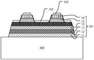
图1a至图1i示出了本发明第一实施例的深紫外发光二极管的制造方法的各阶段截面图;图1j示出了本发明第一实施例中图1c的俯视图。1a to 1i show cross-sectional views at various stages of the manufacturing method of the deep ultraviolet light emitting diode according to the first embodiment of the present invention; and FIG. 1j shows the top view of FIG. 1c in the first embodiment of the present invention.
参考图1a,在第一衬底100的表面形成外延层101。Referring to FIG. 1 a , an
在该步骤中,采用金属化学气相沉积、激光辅助分子束外延、激光溅射,或氢化物气相外延等外延生长工艺在第一衬底100的表面形成外延层101。外延层101沿垂直于第一衬底100表面的方向从下到上依次包括缓冲层11,非故意掺杂层12,超晶格层13,第一半导体层14,多量子阱层15以及第二半导体层16。In this step, an
在该实施例中,第一衬底100例如为蓝宝石衬底。具体的,该蓝宝石衬底包含但不限于镜面蓝宝石衬底或微米级/纳米级图形化蓝宝石衬底中的一种,其优选方案是纳米级图形化蓝宝石衬底。In this embodiment, the
在该实施例中,外延层101可以是多晶或单晶结构,包含以AlGaN/AlInGaN等材料体系组成的往复连续递进式LED外延结构中的一种或几种,其优选方案是含不同Al组分的AlGaN结构。在该实施例中,缓冲层11的材料例如为AlN,非故意掺杂层12的材料例如为AlN,超晶格层13的材料例如为AlN/AlGaN,第一半导体层14的材料例如为重掺杂的n-AlGaN,多量子阱层15的材料例如为AlGaN或AlGaInN,对应的波长范围为200nm~320nm,第二半导体层16的材料例如为p-AlGaN,外延层101的总厚度例如为5-10um。In this embodiment, the
在其他实施例中,第一衬底100还可以是同质或异质衬底中的一种,包括GaN、AlN、Ga2O3、SiC、Si、蓝宝石、ZnO单晶衬底,以及带有预沉积AlN膜的耐高温金属衬底,其晶圆尺寸为1英寸到8英寸中的一种,衬底厚度为300um到2mm。In other embodiments, the
进一步地,在外延层101上形成第一台阶,如图1b所示。Further, a first step is formed on the
在该步骤中,采用光刻工艺和干法蚀刻工艺对多量子阱层15和第二半导体层16进行蚀刻,形成第一台阶。In this step, the multiple
在该实施例中,部分多量子阱层15和第二半导体层16被蚀刻,从而暴露第一半导体层14的表面,剩余的多量子阱层15和第二半导体层16相互分隔,形成多个俯视图案为正六边形的棱台。第一台阶包括上台阶面,下台阶面以及台阶侧壁,上台阶面为棱台中第二半导体层16的表面,下台阶面为第一半导体层14的表面,台阶侧壁为多量子阱层15和第二半导体层16的侧壁,且台阶侧壁具有30°~60°的倾角,优选方案为40°。In this embodiment, part of the multiple
在该实施例中,第一台阶例如为多量子阱层15和第二半导体层16组成的凸台形成的,多个凸台相互分隔。凸台的形状例如可以为圆台、正多边形棱台或其他多边形棱台中的任意一种,第一台阶的数量不少于2个,且呈阵列式均匀分布。多量子阱层的面积占整个衬底面积的50%~85%。In this embodiment, the first step is formed by, for example, a boss composed of the multiple
在其他实施例中,第一台阶还可以是贯穿所述多量子阱层和所述第二半导体层的通孔,多个通孔相互分隔。In other embodiments, the first step may also be a through hole passing through the multiple quantum well layer and the second semiconductor layer, and a plurality of through holes are separated from each other.
进一步地,在第一台阶的侧壁形成粗化表面,以及去除部分外延层101,形成第二台阶,如图1c所示。Further, a roughened surface is formed on the sidewall of the first step, and part of the
在该步骤中,对第一台阶进行图案化的MESA光刻,设计凹凸的图形线条从而在第一台阶的侧壁形成凹凸结构,该凹凸结构包括凸起结构和凹陷结构,具有凹凸不平的表面,从而增加了第一台阶的侧壁面积,该凹凸结构在第一台阶的侧壁形成在竖直方向上的图案。进一步地,还包括采用光刻工艺和干法蚀刻工艺对第一台阶以外的外延层101进行深槽蚀刻,形成第二台阶,从而暴露第一衬底100的表面。In this step, patterned MESA lithography is performed on the first step, and concave-convex pattern lines are designed to form a concave-convex structure on the sidewall of the first step. The concave-convex structure includes a convex structure and a concave structure, and has an uneven surface. , thereby increasing the sidewall area of the first step, and the concave-convex structure forms a pattern in the vertical direction on the sidewall of the first step. Further, the method further includes performing deep trench etching on the
第二台阶包括缓冲层11,非故意掺杂层12,超晶格层13和第一半导体层14,第一台阶位于第二台阶上。第二台阶的上台阶面例如为第一半导体层14的表面,第二台阶的侧表面例如为缓冲层11,非故意掺杂层12,超晶格层13和第一半导体层14的侧壁,第二台阶的下台阶面为第一衬底100的表面。The second step includes a buffer layer 11, an unintentionally doped
在该实施例中,图1j为图1c的俯视图,图1c例如为沿图1j中虚线AA所示的位置进行的截面图。在图1j中,标号132为第一台阶的下台阶面的边缘,第一台阶的俯视形状例如为正六边形,第一台阶的侧壁具有凹凸结构(图中未示出),标号131为深槽蚀刻的边缘,深槽蚀刻的边缘外侧为第一衬底100。图1j中示出了具有四个第一台阶的实施例,该四个第一台阶位于一个第二台阶上,在其他实施例中,第一台阶的数量还可以是2个或6个或8个等,本实施例对此不作限制,且多个第一台阶阵列式均匀分布。In this embodiment, FIG. 1 j is a top view of FIG. 1 c , and FIG. 1 c is, for example, a cross-sectional view taken along the position indicated by the dashed line AA in FIG. 1 j . In FIG. 1j, the
在该实施例中,第一台阶侧壁的凹凸结构中凸起或者凹陷的形状为三角形、圆形、梯形或具有凸起或凹陷特征的规则设计的图形中一种或多种组合,尺寸在数微米到数百微米之间。In this embodiment, the convex or concave shape of the concave-convex structure on the sidewall of the first step is one or more combinations of triangles, circles, trapezoids, or regularly designed figures with convex or concave features, and the size is between a few microns and hundreds of microns.
进一步地,在第一半导体层14的表面形成第一欧姆接触层102,如图1d所示。Further, a first
在该步骤中,采用光刻工艺和电子束蒸发工艺在第一台阶边缘之外的第一半导体层14的表面上形成金属材料,并在氮气(N2)氛围和900℃的条件下快速退火从而形成良好的N型欧姆接触。第一欧姆接触层102的材料例如为Cr、Al、Ni或Au等金属材料中的一种或多种组合,厚度范围为100nm~2um。In this step, a metal material is formed on the surface of the
在其他实施例中,第一欧姆接触层102的材料为V、Ti、Cr、Al、Ni、Au、Pt中的一种或多种组合,退火温度范围为800~1100℃,退火时间范围为30s~2min。第一欧姆接触层102例如为N型欧姆接触层,第一半导体层14例如为N型半导体层。In other embodiments, the material of the first
进一步地,在第二半导体层16的表面形成第二欧姆接触层103,如图1e所示。Further, a second
在该步骤中,采用光刻和电子束蒸发工艺在第一台阶的第二半导体层16的表面形成第二欧姆接触层103,并在O2氛围和600℃条件下快速退火形成良好的P型欧姆接触。第二欧姆接触层103的材料例如为NiAu,厚度范围为0.1nm~100nm。同时,第二欧姆接触层103可以反射部分光,具有反射镜的功能。In this step, the second
在其他实施例中,第二欧姆接触层103的材料还可以是ITO、Ni、NiAu、Pd、Rh中的一种或多种组合,退火氛围为空气或氧气中的一种,退火温度范围为350~700℃,退火时间范围为3~10min。第二欧姆接触层103例如为P型欧姆接触层,第二半导体层16例如为P型半导体层。In other embodiments, the material of the second
进一步地,在半导体结构的表面形成介质层105,如图1f所示。Further, a
在该步骤中,采用化学气相沉积(Chemical Vapour Deposition,CVD)工艺在半导体结构的表面形成介质层105。介质层105的材料例如SiNx。In this step, a chemical vapor deposition (Chemical Vapour Deposition, CVD) process is used to form a
在形成介质层105的步骤之后,还包括采用光刻和干法蚀刻工艺去除部分第二欧姆接触层103和部分第一欧姆接触层102表面的介质层105,从而使部分第二欧姆接触层103和部分第一欧姆接触层102的表面暴露。此时,介质层105覆盖第一台阶的侧壁、第二台阶的侧壁、第一半导体层以及第二半导体层的表面。After the step of forming the
在其他实施例中,介质层105的材料还可以为SiO2、SiNx、Al2O3、AlN、MgF2、HfO2材料中的一种或多种组合,厚度范围为30nm~5um。In other embodiments, the material of the
优选地,介质层105的材料为高导热介质材料,包括BN、AlN、BeO或金刚石薄膜中的一种或多种组合,其厚度为100nm到5um,其制备方法为溅射、RPD(reactive plasmadeposition,反应等离子体沉积)、ALD(atomic layer deposition,原子层沉积)中的一种或多种组合。在该实施例中,采用高导热介质材料,能够提高深紫外发光二极管的散热性能,从而提高紫外发光二极管的可靠性。Preferably, the material of the
进一步地,在半导体结构的表面形成反射镜层104,如图1g所示。Further, a
在该步骤中,采用溅射工艺在介质层105、第二欧姆接触层103,以及第二台阶底部的第一衬底100的表面形成反射镜层104。反射镜层104的材料例如为AlTiPt。In this step, a
在该实施例中,还包括采用剥离工艺去除第二欧姆接触层103表面的反射镜层104,使第二欧姆接触层103的表面暴露,保证第二欧姆接触层103与第一欧姆接触层102之间绝缘。In this embodiment, the
在其他实施例中,反射镜层104的材料还可以是Al、Rh、Pt、DBR、ODR中的一种或多种组合,厚度范围为100nm-3um。In other embodiments, the material of the
进一步地,在半导体结构的表面形成钝化层107,并形成暴露第一欧姆接触层102和反射镜层104的通孔121,如图1h所示。Further, a
在该步骤中,采用等离子体化学气相沉积(Plasma Enhanced Chemical VaporDeposition,PECVD)工艺在半导体结构的表面形成钝化层107。钝化层107用于保护半导体结构,材料例如为SiO2,厚度例如为2000nm。In this step, a plasma chemical vapor deposition (Plasma Enhanced Chemical Vapor Deposition, PECVD) process is used to form a
采用光刻工艺和干法蚀刻工艺在钝化层107中形成多个通孔121,多个通孔121分别暴露第二欧姆接触层103的表面和反射镜层104的表面。A plurality of through holes 121 are formed in the
进一步地,在钝化层107上形成第一电极108和第二电极109,如图1i所示。Further, a
在该步骤中,采用电子束蒸发工艺在多个通孔121中和钝化层107上沉积导电材料,并通过剥离工艺将钝化层107表面连接的部分导电材料剥离去除,从而形成互相分隔的第一电极108和第二电极109。在该实施例中,第一电极108和第二电极109的材料例如为AuSn。第一电极108例如为N电极,第二电极109例如为P电极。In this step, a conductive material is deposited in the plurality of through holes 121 and on the
在该实施例中,深紫外发光二极管为倒装结构的深紫外发光二极管,通过形成阵列分布的第一台阶以及在第一台阶的侧壁形成粗化表面,在不损失发光区面积的前提下,增加了深紫外发光二极管的侧壁面积,从而提高了以水平方向为主要出光方向的深紫外发光二极管的侧壁光提取效率,并且第一台阶侧壁的粗化表面还可以改善电流扩展效果。In this embodiment, the deep ultraviolet light emitting diode is a deep ultraviolet light emitting diode with a flip-chip structure. By forming the first step of the array distribution and forming the roughened surface on the sidewall of the first step, the area of the light emitting area is not lost. , increasing the sidewall area of the deep ultraviolet light emitting diode, thereby improving the sidewall light extraction efficiency of the deep ultraviolet light emitting diode with the horizontal direction as the main light emitting direction, and the roughened surface of the sidewall of the first step can also improve the current spreading effect. .
进一步地,采用高导热的介质材料,可以有效改善深紫外发光二极管的散热能力,从而提高深紫外发光二极管的可靠性。Further, using a dielectric material with high thermal conductivity can effectively improve the heat dissipation capability of the deep ultraviolet light emitting diode, thereby improving the reliability of the deep ultraviolet light emitting diode.
进一步地,形成阵列分布的第一台阶以及在第一台阶的侧壁形成粗化表面的技术方案可用于所有的正装、倒装和垂直结构深紫外发光二极管工艺中,不仅可以降低工艺复杂度,同时具有良好的工艺兼容性,能有效改善深紫外发光二极管的光提取效率偏低和散热性能差的问题。Further, the technical solution of forming the first step of the array distribution and forming the roughened surface on the sidewall of the first step can be used in all front-loading, flip-chip and vertical structure deep ultraviolet light emitting diode processes, which can not only reduce the process complexity, At the same time, it has good process compatibility, and can effectively improve the problems of low light extraction efficiency and poor heat dissipation performance of deep ultraviolet light emitting diodes.
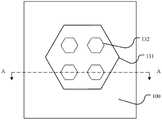
图2a至图2f示出了本发明第二实施例的深紫外发光二极管的制造方法的各阶段截面图;图2g示出了本发明第二实施例中图2b的俯视图。在该实施例中,深紫外发光二极管为倒装通孔的深紫外发光二极管。2a to 2f show cross-sectional views at various stages of the manufacturing method of the deep ultraviolet light emitting diode according to the second embodiment of the present invention; and FIG. 2g shows the top view of FIG. 2b in the second embodiment of the present invention. In this embodiment, the deep ultraviolet light emitting diode is a deep ultraviolet light emitting diode with a flip-chip through hole.
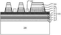
参考图2a,在第一衬底200的表面形成外延层201。Referring to FIG. 2 a , an
在该步骤中,采用金属化学气相沉积、激光辅助分子束外延、激光溅射,或氢化物气相外延等外延生长工艺在第一衬底200的表面形成外延层201。外延层201沿垂直于第一衬底200表面的方向从下到上依次包括缓冲层21,非故意掺杂层22,超晶格层23,第一半导体层24,多量子阱层25以及第二半导体层26。In this step, an
在该实施例中,第一衬底200例如为蓝宝石衬底。具体的,该蓝宝石衬底包含但不限于镜面蓝宝石衬底或微米级/纳米级图形化蓝宝石衬底中的一种,其优选方案是纳米级图形化蓝宝石衬底。In this embodiment, the
在该实施例中,外延层201可以是多晶或单晶结构,包含以AlGaN/AlInGaN等材料体系组成的往复连续递进式LED外延结构中的一种或几种,其优选方案是含不同Al组分的AlGaN结构。在该实施例中,缓冲层21的材料例如为AlN,非故意掺杂层22的材料例如为AlN,超晶格层23的材料例如为AlN/AlGaN,第一半导体层24的材料例如为重掺杂的n-AlGaN,多量子阱层25的材料例如为AlGaN或AlGaInN,对应的波长范围为200nm~320nm,第二半导体层26的材料例如为p-AlGaN,外延层201的总厚度例如为5-10um。In this embodiment, the
在其他实施例中,第一衬底200还可以是同质或异质衬底中的一种,包括GaN、AlN、Ga2O3、SiC、Si、蓝宝石、ZnO单晶衬底,以及带有预沉积AlN膜的耐高温金属衬底,其晶圆尺寸为1英寸到8英寸中的一种,衬底厚度为300um到2mm。In other embodiments, the
进一步地,在外延层201中形成第一台阶,并在第一台阶的侧壁形成粗化表面,如图2b所示。Further, a first step is formed in the
在该步骤中,采用光刻工艺定义出第一台阶以外的区域,并采用干法蚀刻工艺在第一台阶以外的区域进行蚀刻,即刻蚀第二半导体层26和多量子阱层25形成多个通孔以暴露出第一半导体层24的表面,剩余的多量子阱层25和第二半导体层26连通。第一台阶包括上台阶面,下台阶面以及台阶侧壁,上台阶面为第二半导体层26的表面,下台阶面为通孔中第一半导体层24的表面,台阶侧壁为多量子阱层25和第二半导体层26的侧壁,且台阶侧壁具有30°~60°的倾角,优选方案为40°。In this step, a photolithography process is used to define an area other than the first step, and a dry etching process is used to etch the area outside the first step, that is, the
在该实施例中,第一台阶例如为贯穿所述多量子阱层25和所述第二半导体层26的通孔形成的,多个通孔相互分隔。通孔的形状可以是圆台、正多边形棱台或其他多边形棱台中的任意一种,第一台阶的数量不少于2个,且呈阵列式均匀分布。多量子阱层的面积占整个衬底面积的50%~85%。In this embodiment, the first step is formed by, for example, through holes penetrating the multiple
在其他实施例中,第一台阶例如为多量子阱层和第二半导体层组成的凸台,多个凸台相互分隔。In other embodiments, the first step is, for example, a boss formed by the multiple quantum well layer and the second semiconductor layer, and the plurality of bosses are separated from each other.
参考图2g,图2b例如为沿图2g中虚线BB所示的位置进行的截面图。在图2g中,标号232为第一台阶的下台阶面的边缘,第一台阶的俯视形状例如为正六边形,第一台阶的侧壁具有凹凸结构(图中未示出),第一台阶的侧壁边缘的外侧为第二半导体层26的表面,多量子阱层25和第二半导体层26的外围边缘部分被蚀刻,暴露第一半导体层24的表面。图2g中示出了具有八个第一台阶的实施例,八个第一台阶呈阵列式均匀分布,且大小相同,在其他实施例中,第一台阶的数量还可以是3个、5个等,本实施例对此不做限制,且多个第一台阶呈阵列式均匀分布。Referring to Fig. 2g, Fig. 2b is, for example, a cross-sectional view taken along the position shown by the dashed line BB in Fig. 2g. In FIG. 2g,
在该实施例中,第一台阶均匀分布,且第一台阶的侧壁通过蚀刻形成凹凸结构。该凹凸结构包括凸起结构和凹陷结构,具有凹凸不平的表面,从而增加了第一台阶的侧壁面积。In this embodiment, the first steps are uniformly distributed, and a concave-convex structure is formed on the sidewalls of the first steps by etching. The concave-convex structure includes a convex structure and a concave structure, and has an uneven surface, thereby increasing the sidewall area of the first step.
在该实施例中,第一台阶侧壁的凹凸结构中凸起或者凹陷的形状为三角形、圆形、梯形或具有凸起或凹陷特征的规则设计的图形中一种或多种组合,尺寸在数微米到数百微米之间。In this embodiment, the convex or concave shape of the concave-convex structure on the sidewall of the first step is one or more combinations of triangles, circles, trapezoids, or regularly designed figures with convex or concave features, and the size is between a few microns and hundreds of microns.
进一步地,在第一半导体层24的表面形成第一欧姆接触层202,如图2c所示。Further, a first
在该步骤中,采用光刻和物理气相沉积(Physical Vapor Deposition,PVD)工艺在第一半导体层24的表面沉积金属材料,从而形成第一欧姆接触层202。在该实施例中,还包括在N2氛围和800℃的条件下退火30s~2min使第一欧姆接触层202和第一半导体层24形成良好的欧姆接触。In this step, a metal material is deposited on the surface of the
在该实施例中,第一欧姆接触层202的材料包括V、Al、Ti或Au中的一种或几种的组合。第一欧姆接触层202的厚度为500nm。第一欧姆接触层202例如为N型欧姆接触层,第一半导体层24例如为N型半导体层。In this embodiment, the material of the first
进一步地,在第二半导体层26的表面依次形成第二欧姆接触层203和反射镜层204,如图2d所示。Further, a second
在该步骤中,采用光刻、湿法腐蚀和溅射的工艺在第二半导体层26的表面形成第二欧姆接触层203和反射镜层204。在该实施例中,第二欧姆接触层203的材料为NiAu,厚度为60nm,反射镜层204的材料例如为TiPtAu,厚度例如为600nm。第二欧姆接触层203例如为P型欧姆接触层,第二半导体层26例如为P型半导体层。In this step, the second
在该实施例中,形成后的第二欧姆接触层203和反射镜层204只位于第二半导体层26的表面,且暴露第一欧姆接触层202。In this embodiment, the formed second
进一步地,在半导体结构的表面形成介质层205,并在介质层205中形成暴露第一欧姆接触层202的通孔,如图2e所示。Further, a
在该步骤中,采用溅射工艺在半导体结构的表面形成介质层205,然后采用光刻和干法蚀刻工艺在介质层205中形成多个通孔,部分通孔暴露出第一欧姆接触层202,部分通孔暴露出反射镜层204。In this step, a
在该实施例中,介质层205的材料例如为高导热的BN,厚度为500nm。In this embodiment, the material of the
进一步地,在介质层205上形成第一电极208和第二电极209,如图2f所示。Further, a
在该步骤中,采用溅射工艺在多个通孔中和介质层205上形成电极层,电极层的材料例如为导电金属。在该实施例中,电极层填充第一欧姆接触层202所在的通孔以及暴露出反射镜层204的通孔。In this step, an electrode layer is formed in the plurality of through holes and on the
在该实施例中,还包括采用光刻和剥离工艺去除位于介质层205上的部分电极层,使电极层分隔成与第一欧姆接触层102连接的第一电极208和与反射镜层204连接的第二电极209。In this embodiment, it also includes removing part of the electrode layer on the
在该实施例中,第一电极208例如为N电极,第二电极209例如为P电极。In this embodiment, the
在该实施例中,深紫外发光二极管为倒装通孔的深紫外发光二极管,通过形成阵列分布的第一台阶以及在第一台阶的侧壁形成粗化表面,在不损失发光区面积的前提下,增加了深紫外发光二极管的侧壁面积,从而提高了以水平方向为主要出光方向的深紫外发光二极管的侧壁光提取效率,并且第一台阶侧壁的粗化表面还可以改善电流扩展效果。In this embodiment, the deep ultraviolet light emitting diode is a deep ultraviolet light emitting diode with a flip-chip through hole. By forming the first step of the array distribution and forming the roughened surface on the sidewall of the first step, the area of the light emitting area is not lost. In addition, the sidewall area of the deep ultraviolet light emitting diode is increased, thereby improving the sidewall light extraction efficiency of the deep ultraviolet light emitting diode with the horizontal direction as the main light emitting direction, and the roughened surface of the sidewall of the first step can also improve the current spreading. Effect.
进一步地,采用高导热的介质材料,可以有效改善深紫外发光二极管的散热能力,从而提高深紫外发光二极管的可靠性。Further, using a dielectric material with high thermal conductivity can effectively improve the heat dissipation capability of the deep ultraviolet light emitting diode, thereby improving the reliability of the deep ultraviolet light emitting diode.
进一步地,形成阵列分布的第一台阶以及在第一台阶的侧壁形成粗化表面的技术方案可用于所有的正装、倒装和垂直结构深紫外发光二极管工艺中,不仅可以降低工艺复杂度,同时具有良好的工艺兼容性,能有效改善深紫外发光二极管的光提取效率偏低和散热性能差的问题。Further, the technical solution of forming the first step of the array distribution and forming the roughened surface on the sidewall of the first step can be used in all front-loading, flip-chip and vertical structure deep ultraviolet light emitting diode processes, which can not only reduce the process complexity, At the same time, it has good process compatibility, and can effectively improve the problems of low light extraction efficiency and poor heat dissipation performance of deep ultraviolet light emitting diodes.
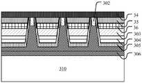
图3a至图3l示出了本发明第三实施例的深紫外发光二极管的制造方法的各阶段截面图;图3m示出了本发明第三实施例中图3b的俯视图。在该实施例中,深紫外发光二极管为垂直通孔的深紫外发光二极管。3a to 3l show cross-sectional views of various stages of the manufacturing method of the deep ultraviolet light emitting diode according to the third embodiment of the present invention; and FIG. 3m shows the top view of FIG. 3b in the third embodiment of the present invention. In this embodiment, the deep ultraviolet light emitting diode is a vertical through hole deep ultraviolet light emitting diode.
参考图3a,在第一衬底300的表面依次形成外延层301。Referring to FIG. 3 a ,
在该步骤中,采用金属化学气相沉积、激光辅助分子束外延、激光溅射,或氢化物气相外延等外延生长工艺在第一衬底300的表面形成外延层301。外延层301沿垂直于第一衬底300表面的方向从下到上依次包括缓冲层31,非故意掺杂层32,超晶格层33,第一半导体层34,多量子阱层35以及第二半导体层36。In this step, an
在该实施例中,第一衬底300例如为蓝宝石衬底。具体的,该蓝宝石衬底包含但不限于镜面蓝宝石衬底或微米级/纳米级图形化蓝宝石衬底中的一种,其优选方案是镜面蓝宝石衬底。In this embodiment, the
在该实施例中,外延层301可以是多晶或单晶结构,包含以AlGaN/AlInGaN等材料体系组成的往复连续递进式LED外延结构中的一种或几种,其优选方案是含不同Al组分的AlGaN结构。在该实施例中,缓冲层31的材料例如为AlN,非故意掺杂层32的材料例如为AlN,超晶格层33的材料例如为AlN/AlGaN,第一半导体层34的材料例如为重掺杂的n-AlGaN,多量子阱层35的材料例如为AlGaN或AlGaInN,对应的波长范围为200nm~320nm,第二半导体层36的材料例如为p-AlGaN,外延层301的总厚度例如为5-10um。In this embodiment, the
进一步地,在外延层301中形成第一台阶,以及在第一台阶的侧壁形成粗化表面,如图3b所示。Further, a first step is formed in the
在该步骤中,采用光刻和干法蚀刻工艺在外延层301中形成均匀阵列分布的第一台阶。蚀刻外延层301形成多个通孔后,暴露出第一半导体层34的表面。具体的,刻蚀第二半导体层36和多量子阱层35形成多个通孔,剩余的多量子阱层35和第二半导体层36连通。在该实施例中,第一台阶包括上台阶面,下台阶面以及台阶侧壁,上台阶面为第二半导体层36的上表面,下台阶面为通孔中第一半导体层34的表面,台阶侧壁为多量子阱层35和第二半导体层36的侧壁,且台阶侧壁具有30°~60°的倾角,优选方案为40°。In this step, the first steps with uniform array distribution are formed in the
在该实施例中,第一台阶例如为贯穿所述多量子阱层35和所述第二半导体层36的通孔形成的,多个通孔相互分隔。通孔的形状可以是圆台、正多边形棱台或其他多边形棱台中的任意一种,第一台阶的数量不少于2个,且呈阵列式均匀分布。多量子阱层的面积占整个衬底面积的50%~85%。In this embodiment, the first step is formed by, for example, through holes penetrating the multiple
在其他实施例中,第一台阶例如为多量子阱层和第二半导体层组成的凸台,多个凸台相互分隔。In other embodiments, the first step is, for example, a boss formed by the multiple quantum well layer and the second semiconductor layer, and the plurality of bosses are separated from each other.
参考图3m,图3b例如为沿图3m中虚线CC所示的位置进行的截面图。在图3m中,标号332为第一台阶的下台阶面的边缘,第一台阶的俯视形状例如为正六边形,第一台阶的侧壁具有凹凸结构(图中未示出),第一台阶的侧壁边缘的外侧为第二半导体层36。图3m中示出了具有九个第一台阶的实施例,该九个第一台阶呈阵列式均匀分布,大小相同,在其他实施例中,第一台阶的数量还可以是4个、6个等,本实施例对此不作限制,且多个第一台阶呈阵列式均匀分布。Referring to Fig. 3m, Fig. 3b is, for example, a cross-sectional view taken along the position shown by the dashed line CC in Fig. 3m. In FIG. 3m,
在该实施例中,第一台阶均匀分布,且第一台阶的侧壁通过蚀刻形成凹凸结构。该凹凸结构包括凸起结构和凹陷结构,具有凹凸不平的表面,从而增加了第一台阶的侧壁面积。In this embodiment, the first steps are uniformly distributed, and a concave-convex structure is formed on the sidewalls of the first steps by etching. The concave-convex structure includes a convex structure and a concave structure, and has an uneven surface, thereby increasing the sidewall area of the first step.
在该实施例中,第一台阶侧壁的凹凸结构中凸起或者凹陷的形状为三角形、圆形、梯形或具有凸起或凹陷特征的规则设计的图形中一种或多种组合,尺寸在数微米到数百微米之间。In this embodiment, the convex or concave shape of the concave-convex structure on the sidewall of the first step is one or more combinations of triangles, circles, trapezoids, or regularly designed figures with convex or concave features, and the size is between a few microns and hundreds of microns.
进一步地,在第一半导体层34的表面形成第一欧姆接触层302,如图3c所示。Further, a first
在该实施例中,例如采用光刻和物理气相沉积工艺在第一半导体层34的表面形成第一欧姆接触层302,并在氮气氛围和800℃条件下快速退火30s~2min使第一欧姆接触层302与第一半导体层34形成良好的欧姆接触。In this embodiment, the first
在该实施例中,第一欧姆接触层302的材料包括V、Al、Ti或Au中的一种或几种的组合。第一欧姆接触层302的厚度为500nm。第一欧姆接触层302例如为N型欧姆接触层,第一半导体层34例如为N型半导体层。In this embodiment, the material of the first
进一步地,在第二半导体层36的表面依次形成第二欧姆接触层303和反射镜层304,如图3d所示。Further, a second
在该步骤中,采用光刻、湿法腐蚀和溅射工艺在第二半导体层36的表面形成第二欧姆接触层303和反射镜层304。在该实施例中,第二欧姆接触层303的材料为NiAl,厚度为120nm,反射镜层304的材料例如为TiPtAu,厚度例如为200nm。第二欧姆接触层303例如为P型欧姆接触层,第二半导体层36例如为P型半导体层。In this step, the second
在该实施例中,形成后的第二欧姆接触层303和反射镜层304只位于第二半导体层36的表面,且暴露第一欧姆接触层302。In this embodiment, the formed second
进一步地,在半导体结构的表面形成介质层305,并去除第一欧姆接触层302表面的介质层305,如图3e所示。Further, a
在该步骤中,采用ALD原子层沉积工艺在半导体结构的表面形成介质层305,以及采用光刻和干法蚀刻工艺去除第一欧姆接触层302表面的介质层305。在该实施例中,去除第一欧姆接触层302表面的介质层305之后,剩余的介质层305位于反射镜层304的表面、第一台阶的侧壁、反射镜层304以及第二欧姆接触层303的侧壁,介质层305用于隔离第一欧姆接触层302与多量子阱层35、第二半导体层36、第二欧姆接触层303以及反射镜层304。In this step, the ALD atomic layer deposition process is used to form the
在该实施例中,介质层305的材料为高导热介质材料,例如为AlN,厚度例如为500nm。In this embodiment, the material of the
进一步地,在半导体结构的表面形成键合层306,得到第一半导体结构,如图3f所示。Further, a
在该步骤中,采用溅射工艺在半导体结构的表面形成键合层306,键合层306例如为Cu/Sn二元金属键合层,具体的,键合层306例如为一对Au和Sn二元金属层形成的键合层,键合层306中各金属层的厚度例如为Cu金属层1um,Sn金属层200nm。In this step, a sputtering process is used to form a
在该实施例中,在形成键合层306之前,还可以在半导体表面形成粘附层(图中未示出),粘附层位于键合层306与半导体结构之间,用于粘合半导体结构与键合层306。粘附层的材料例如为Ti,厚度例如为200nm。In this embodiment, before the
进一步地,在第二衬底310上形成粘附层(图中未示出)和键合层306,得到第二半导体结构,并将第一半导体结构与第二半导体结构键合,如图3g所示。Further, an adhesive layer (not shown in the figure) and a
在该实施例中,第二衬底310上形成的粘附层(图中未示出)的材料例如为Ti,厚度例如为200nm。键合层306例如为Cu/Sn二元金属键合层,具体的,键合层306例如为一对Cu和Sn二元金属层形成的键合层,键合层306中各金属层的厚度例如为Cu金属层1um,Sn金属层200nm。In this embodiment, the material of the adhesion layer (not shown in the figure) formed on the
在该实施例中,第二衬底310例如为CuW衬底,第二衬底310的厚度例如为400um。第一半导体结构和第二半导体结构在260℃条件下,采用CuSn液相瞬态键合工艺进行键合。In this embodiment, the
在该实施例中,第二衬底310为第一电极,第一电极为N电极。In this embodiment, the
进一步地,去除第一衬底300以及部分外延层301,如图3h所示。Further, the
在该步骤中,例如采用波长为266nm,面积为50um的紫外激光小光斑,将超晶格层33进行剥离分解,从而实现第一衬底300、缓冲层31、非故意掺杂层32以及超晶格层33与其他部分的分离。In this step, for example, a small ultraviolet laser spot with a wavelength of 266 nm and an area of 50 μm is used to peel off and decompose the
在该实施例中,还包括用稀盐酸处理剥离超晶格层33后暴露的第一半导体层34的表面。In this embodiment, the surface of the
进一步地,对第一半导体层34的表面进行粗化处理,如图3i所示。Further, roughening treatment is performed on the surface of the
在该步骤中,例如采用6mol/L浓度的KOH溶液,在70℃条件下处理第一半导体层34的表面形成粗化表面,从而利用二次微纳结构增加深紫外发光二极管的出光。In this step, for example, a KOH solution with a concentration of 6 mol/L is used to treat the surface of the
进一步地,在第一半导体层34的表面形成第三台阶,以及在第三台阶的侧壁形成粗化表面,如图3j所示。Further, a third step is formed on the surface of the
在该步骤中,利用光刻和干法蚀刻工艺去除半导体结构边缘的部分第一半导体层34、多量子阱35、第二半导体层36以及第二欧姆接触层303,暴露出反射镜层304的表面,从而在半导体结构中形成第三台阶。在该实施例中,第三台阶的下台阶面区域的宽度例如为100um。In this step, part of the
在该实施例中,第三台阶包括第一半导体层34,多量子阱层35,第二半导体层36以及第二欧姆接触层303。第三台阶的上台阶面为经过粗化处理的第一半导体层34的表面,台阶侧壁为第一半导体层34,多量子阱层35,第二半导体层36以及第二欧姆接触层303的侧壁,下台阶面为反射镜层304的表面。In this embodiment, the third step includes the
在该实施例中,还包括采用蚀刻工艺在第三台阶的侧壁形成凹凸结构,该凹凸结构包括凸起结构和凹陷结构,具有凹凸不平的表面,从而增加了第一台阶的侧壁面积。In this embodiment, an etching process is also used to form a concave-convex structure on the sidewall of the third step, the concave-convex structure includes a convex structure and a concave structure, and has an uneven surface, thereby increasing the sidewall area of the first step.
在该实施例中,第一台阶侧壁的凹凸结构中凸起或者凹陷的形状为三角形、圆形、梯形或具有凸起或凹陷特征的规则设计的图形中一种或多种组合,尺寸在数微米到数百微米之间。In this embodiment, the convex or concave shape of the concave-convex structure on the sidewall of the first step is one or more combinations of triangles, circles, trapezoids, or regularly designed figures with convex or concave features, and the size is between a few microns and hundreds of microns.
进一步地,在半导体结构的表面形成钝化层307,如图3k所示。Further, a
在该步骤中,采用等离子体气相沉积(PECVD)工艺在半导体结构的表面形成钝化层307,以及采用光刻和干法蚀刻工艺去除反射镜层304表面的钝化层307,剩余的钝化层307位于第三台阶的侧壁以及第一半导体层34的表面。In this step, a
在该实施例中,钝化层307的材料为SiO2,厚度为200nm。In this embodiment, the material of the
进一步地,在台阶区域的反射镜层304的表面形成第二电极309,如图3l所示。Further, a
在该步骤中,采用光刻、湿法腐蚀和电子束蒸发技术,在反射镜层304的表面上形成第二电极309。第二电极309的材料例如为CrPtAu。第二电极309例如为P电极。In this step, a
在该实施例中,深紫外发光二极管为垂直通孔的深紫外发光二极管,通过形成阵列分布的第一台阶以及在第一台阶和第三台阶的侧壁形成粗化表面,在不损失发光区面积的前提下,增加了深紫外发光二极管的侧壁面积,从而提高了以水平方向为主要出光方向的深紫外发光二极管的侧壁光提取效率,并且第一台阶侧壁的粗化表面还可以改善电流扩展效果。In this embodiment, the deep ultraviolet light emitting diode is a deep ultraviolet light emitting diode with a vertical through hole. By forming the first step of the array distribution and forming the roughened surface on the sidewalls of the first step and the third step, the light emitting area is not lost. On the premise of the area, the side wall area of the deep ultraviolet light emitting diode is increased, thereby improving the side wall light extraction efficiency of the deep ultraviolet light emitting diode with the horizontal direction as the main light emitting direction, and the roughened surface of the first step side wall can also be Improve current spreading effect.
进一步地,采用高导热的介质材料,可以有效改善深紫外发光二极管的散热能力,从而提高深紫外发光二极管的可靠性。Further, using a dielectric material with high thermal conductivity can effectively improve the heat dissipation capability of the deep ultraviolet light emitting diode, thereby improving the reliability of the deep ultraviolet light emitting diode.
进一步地,形成阵列分布的第一台阶以及在第一台阶的侧壁形成粗化表面的技术方案可用于所有的正装、倒装和垂直结构深紫外发光二极管工艺中,不仅可以降低工艺复杂度,同时具有良好的工艺兼容性,能有效改善深紫外发光二极管的光提取效率偏低和散热性能差的问题。Further, the technical solution of forming the first step of the array distribution and forming the roughened surface on the sidewall of the first step can be used in all front-loading, flip-chip and vertical structure deep ultraviolet light emitting diode processes, which can not only reduce the process complexity, At the same time, it has good process compatibility, and can effectively improve the problems of low light extraction efficiency and poor heat dissipation performance of deep ultraviolet light emitting diodes.
依照本发明的实施例如上文所述,这些实施例并没有详尽叙述所有的细节,也不限制该发明仅为所述的具体实施例。显然,根据以上描述,可作很多的修改和变化。本说明书选取并具体描述这些实施例,是为了更好地解释本发明的原理和实际应用,从而使所属技术领域技术人员能很好地利用本发明以及在本发明基础上的修改使用。本发明仅受权利要求书及其全部范围和等效物的限制。Embodiments in accordance with the present invention are described above, but these embodiments do not exhaust all the details and do not limit the invention to only the specific embodiments described. Obviously, many modifications and variations are possible in light of the above description. This specification selects and specifically describes these embodiments in order to better explain the principle and practical application of the present invention, so that those skilled in the art can make good use of the present invention and modifications based on the present invention. The present invention is to be limited only by the claims and their full scope and equivalents.
Claims (37)
Priority Applications (1)
| Application Number | Priority Date | Filing Date | Title |
|---|---|---|---|
| CN202011283746.XACN112510126B (en) | 2020-11-17 | 2020-11-17 | Deep ultraviolet light emitting diode and manufacturing method thereof |
Applications Claiming Priority (1)
| Application Number | Priority Date | Filing Date | Title |
|---|---|---|---|
| CN202011283746.XACN112510126B (en) | 2020-11-17 | 2020-11-17 | Deep ultraviolet light emitting diode and manufacturing method thereof |
Publications (2)
| Publication Number | Publication Date |
|---|---|
| CN112510126A CN112510126A (en) | 2021-03-16 |
| CN112510126Btrue CN112510126B (en) | 2022-07-29 |
Family
ID=74956500
Family Applications (1)
| Application Number | Title | Priority Date | Filing Date |
|---|---|---|---|
| CN202011283746.XAActiveCN112510126B (en) | 2020-11-17 | 2020-11-17 | Deep ultraviolet light emitting diode and manufacturing method thereof |
Country Status (1)
| Country | Link |
|---|---|
| CN (1) | CN112510126B (en) |
Families Citing this family (9)
| Publication number | Priority date | Publication date | Assignee | Title |
|---|---|---|---|---|
| CN113594305B (en)* | 2021-06-11 | 2023-01-31 | 厦门士兰明镓化合物半导体有限公司 | Manufacturing method of vertical structure LED chip |
| CN113594310B (en)* | 2021-06-11 | 2023-09-08 | 厦门士兰明镓化合物半导体有限公司 | Deep ultraviolet LED chip and manufacturing method thereof |
| CN113594312B (en)* | 2021-06-11 | 2023-10-24 | 厦门士兰明镓化合物半导体有限公司 | Deep ultraviolet LED chip and manufacturing method thereof |
| US20240332453A1 (en)* | 2021-09-14 | 2024-10-03 | Lg Electronics Inc. | Semiconductor light emitting element and display device |
| CN113964249A (en)* | 2021-09-15 | 2022-01-21 | 厦门士兰明镓化合物半导体有限公司 | Light emitting diode and method for manufacturing the same |
| CN114824010B (en)* | 2022-04-28 | 2025-09-12 | 厦门士兰明镓化合物半导体有限公司 | Light emitting diode and manufacturing method thereof |
| CN115347091A (en)* | 2022-04-28 | 2022-11-15 | 厦门士兰明镓化合物半导体有限公司 | A light emitting diode and its manufacturing method |
| CN114975713A (en)* | 2022-05-06 | 2022-08-30 | 厦门士兰明镓化合物半导体有限公司 | A kind of manufacturing method of light-emitting diode and light-emitting diode |
| CN117995954A (en)* | 2024-04-07 | 2024-05-07 | 江西求是高等研究院 | Micro display chip preparation method and micro display chip |
Citations (6)
| Publication number | Priority date | Publication date | Assignee | Title |
|---|---|---|---|---|
| CN101305477A (en)* | 2006-01-09 | 2008-11-12 | 首尔Opto仪器股份有限公司 | Light emitting diode with indium tin oxide layer and manufacturing method thereof |
| CN103165775A (en)* | 2013-04-07 | 2013-06-19 | 中国科学院半导体研究所 | A kind of ultraviolet light-emitting diode with high reflection film and its manufacturing method |
| CN106299050A (en)* | 2016-11-17 | 2017-01-04 | 河北工业大学 | A kind of deep ultraviolet semiconductor light-emitting-diode and preparation method thereof |
| US10091850B2 (en)* | 2015-06-26 | 2018-10-02 | Seoul Semiconductor Co., Ltd. | Backlight unit using multi-cell light emitting diode |
| CN108987546A (en)* | 2013-09-24 | 2018-12-11 | 首尔伟傲世有限公司 | Light emitting diode, light-emitting diode (LED) module and the method for manufacturing light emitting diode |
| CN110690327A (en)* | 2019-09-11 | 2020-01-14 | 佛山市国星半导体技术有限公司 | A kind of preparation method of high-brightness violet LED chip and LED chip |
Family Cites Families (1)
| Publication number | Priority date | Publication date | Assignee | Title |
|---|---|---|---|---|
| CN111599906B (en)* | 2020-05-12 | 2021-05-18 | 武汉大学 | A kind of manufacturing method of vertical structure deep ultraviolet LED chip |
- 2020
- 2020-11-17CNCN202011283746.XApatent/CN112510126B/enactiveActive
Patent Citations (6)
| Publication number | Priority date | Publication date | Assignee | Title |
|---|---|---|---|---|
| CN101305477A (en)* | 2006-01-09 | 2008-11-12 | 首尔Opto仪器股份有限公司 | Light emitting diode with indium tin oxide layer and manufacturing method thereof |
| CN103165775A (en)* | 2013-04-07 | 2013-06-19 | 中国科学院半导体研究所 | A kind of ultraviolet light-emitting diode with high reflection film and its manufacturing method |
| CN108987546A (en)* | 2013-09-24 | 2018-12-11 | 首尔伟傲世有限公司 | Light emitting diode, light-emitting diode (LED) module and the method for manufacturing light emitting diode |
| US10091850B2 (en)* | 2015-06-26 | 2018-10-02 | Seoul Semiconductor Co., Ltd. | Backlight unit using multi-cell light emitting diode |
| CN106299050A (en)* | 2016-11-17 | 2017-01-04 | 河北工业大学 | A kind of deep ultraviolet semiconductor light-emitting-diode and preparation method thereof |
| CN110690327A (en)* | 2019-09-11 | 2020-01-14 | 佛山市国星半导体技术有限公司 | A kind of preparation method of high-brightness violet LED chip and LED chip |
Also Published As
| Publication number | Publication date |
|---|---|
| CN112510126A (en) | 2021-03-16 |
Similar Documents
| Publication | Publication Date | Title |
|---|---|---|
| CN112510126B (en) | Deep ultraviolet light emitting diode and manufacturing method thereof | |
| US20240042166A1 (en) | Semiconductor light-emitting device | |
| US10297720B2 (en) | Light emitting diode and method of manufacturing the same | |
| US8674375B2 (en) | Roughened high refractive index layer/LED for high light extraction | |
| US8735185B2 (en) | Light emitting device and fabrication method thereof | |
| JP4996706B2 (en) | Semiconductor light emitting device and manufacturing method thereof | |
| US8772805B2 (en) | High efficiency light emitting diode and method for fabricating the same | |
| TWI575773B (en) | Contact for a semiconductor light emitting device | |
| US8390007B2 (en) | Semiconductor light emitting device and method of fabricating semiconductor light emitting device | |
| US11764332B2 (en) | Semiconductor light-emitting device | |
| US12155019B2 (en) | Light-emitting device | |
| TW202029521A (en) | Light-emitting device | |
| CN108933187A (en) | A kind of light-emitting surface is the LED chip and preparation method thereof of specific plane geometric figure | |
| GB2547123A (en) | LED vertical chip structure with special coarsening morphology and preparation method therefor | |
| CN112038455A (en) | Ultraviolet light emitting diode and manufacturing method thereof | |
| WO2023273373A1 (en) | Deep-ultraviolet led chip having a vertical structure, manufacturing method, and epitaxial structure | |
| JP2022516669A (en) | Vertical structure blue light emitting diode and its manufacturing method | |
| CN110021689A (en) | Light emitting diode and its manufacturing method | |
| CN104681678A (en) | LED (light emitting diode) with dual-reflector structure and manufacturing method of LED with dual-reflector structure | |
| WO2012040978A1 (en) | Light emitting device and manufacturing method thereof | |
| US9306120B2 (en) | High efficiency light emitting diode | |
| CN111697114A (en) | LED chip with vertical structure and preparation method thereof | |
| CN105914274A (en) | Side-wall-coarsened high-brightness light emitting diode and preparation method thereof | |
| CN114975724B (en) | Flip-chip light emitting diode and method for preparing the same | |
| KR100650990B1 (en) | Nitride semiconductor light emitting diode and method of manufacturing the same |
Legal Events
| Date | Code | Title | Description |
|---|---|---|---|
| PB01 | Publication | ||
| PB01 | Publication | ||
| SE01 | Entry into force of request for substantive examination | ||
| SE01 | Entry into force of request for substantive examination | ||
| CB03 | Change of inventor or designer information | Inventor after:Fan Weihong Inventor after:Li Dongsheng Inventor after:Zhang Xiaoping Inventor after:Ma Xingang Inventor after:Gao Moran Inventor after:Zhao Jinchao Inventor before:Fan Weihong Inventor before:Xue Tuo Inventor before:Li Dongsheng Inventor before:Zhang Xiaoping Inventor before:Ma Xingang Inventor before:Gao Moran Inventor before:Zhao Jinchao | |
| CB03 | Change of inventor or designer information | ||
| GR01 | Patent grant | ||
| GR01 | Patent grant | ||
| TR01 | Transfer of patent right | Effective date of registration:20241202 Address after:310018 No. 10 Street (East) 308, Hangzhou economic and Technological Development Zone, Hangzhou, Zhejiang. Patentee after:HANGZHOU SILAN INTEGRATED CIRCUIT Co.,Ltd. Country or region after:China Patentee after:Xiamen Shiming gallium compound semiconductor Co.,Ltd. Address before:310018 1st floor, building 1, No. 300, Baiyang street, Hangzhou Economic and Technological Development Zone, Hangzhou City, Zhejiang Province Patentee before:HANGZHOU SILAN AZURE Co.,Ltd. Country or region before:China Patentee before:Xiamen Shiming gallium compound semiconductor Co.,Ltd. | |
| TR01 | Transfer of patent right |