Movatterモバイル変換


[0]ホーム

URL:


CN112491373B - A V-band 160W solid-state power synthesis amplifier - Google Patents

A V-band 160W solid-state power synthesis amplifier
Download PDF

Info

Publication number
CN112491373B
CN112491373BCN202011296741.0ACN202011296741ACN112491373BCN 112491373 BCN112491373 BCN 112491373BCN 202011296741 ACN202011296741 ACN 202011296741ACN 112491373 BCN112491373 BCN 112491373B
Authority
CN
China
Prior art keywords
pin
power amplifier
power
module
input
Prior art date
Legal status (The legal status is an assumption and is not a legal conclusion. Google has not performed a legal analysis and makes no representation as to the accuracy of the status listed.)
Active
Application number
CN202011296741.0A
Other languages
Chinese (zh)
Other versions
CN112491373A (en
Inventor
陈冠军
魏伟
王雷
刘羊羊
薛腾
邵占英
Current Assignee (The listed assignees may be inaccurate. Google has not performed a legal analysis and makes no representation or warranty as to the accuracy of the list.)
CETC 54 Research Institute
Original Assignee
CETC 54 Research Institute
Priority date (The priority date is an assumption and is not a legal conclusion. Google has not performed a legal analysis and makes no representation as to the accuracy of the date listed.)
Filing date
Publication date
Application filed by CETC 54 Research InstitutefiledCriticalCETC 54 Research Institute
Priority to CN202011296741.0ApriorityCriticalpatent/CN112491373B/en
Publication of CN112491373ApublicationCriticalpatent/CN112491373A/en
Application grantedgrantedCritical
Publication of CN112491373BpublicationCriticalpatent/CN112491373B/en
Activelegal-statusCriticalCurrent
Anticipated expirationlegal-statusCritical

Links

Images

Classifications

Landscapes

Abstract

Translated fromChinese

本发明公开了一种V频段160W固态功率合成放大器,属于卫星通信技术领域。它由输入隔离器、控制衰减器、预失真模块、驱动放大器、固态功放模块、波导耦合器、检波器、监控单元、温度传感器、电源模块、风机等组成。本发明采用空间功率合成方式将八个功率芯片进行合成,构成一个功放小模块,再采用四路波导E‑T型结构的二进制功率分配/合成网络将四个功放小模块进行合成,最后采用魔T结构的功率分配/合成网络将信号合成达到160W的功率输出。该功率放大器具有频段高、体积小、重量轻、集成化程度高、性能稳定可靠、易维护、工作温度范围宽的特点,特别适用于卫星通信微波信道的功率放大业务。

Figure 202011296741

The invention discloses a V-band 160W solid-state power synthesis amplifier, which belongs to the technical field of satellite communication. It consists of input isolator, control attenuator, predistortion module, drive amplifier, solid-state power amplifier module, waveguide coupler, detector, monitoring unit, temperature sensor, power module, fan, etc. The invention adopts the space power synthesis method to synthesize eight power chips to form a small power amplifier module, and then adopts the binary power distribution/synthesis network of the four-way waveguide E-T structure to synthesize the four small power amplifier modules, and finally uses a magic power amplifier module. The power distribution/combining network of the T-structure combines the signals to achieve a power output of 160W. The power amplifier has the characteristics of high frequency band, small size, light weight, high degree of integration, stable and reliable performance, easy maintenance, and wide operating temperature range, and is especially suitable for the power amplification business of satellite communication microwave channels.

Figure 202011296741

Description

Translated fromChinese
一种V频段160W固态功率合成放大器A V-band 160W solid-state power synthesis amplifier

技术领域technical field

本发明涉及卫星通信技术领域,特别是指一种V频段160W固态功率合成放大器,可用于卫星通信微波信道的功率放大设备。The invention relates to the technical field of satellite communication, in particular to a V-band 160W solid-state power synthesis amplifier, which can be used for power amplifying equipment of a microwave channel of satellite communication.

背景技术Background technique

近年来,随着卫星通信系统的快速发展,对于高频率、高效率、宽频带大功率固态功放的需求与日俱增。然而,单个固态器件在微波毫米波频段输出的功率有限,不能满足系统的需求。为了获得更大的输出功率,常常需要采用功率合成措施。例如,将多个功率器件集中在一个功率合成放大器中。另一方面,出于经济和可靠性等方面的考虑,通常采用较小的功率源进行合成,而不直接采用一个大的功率源。这样,除了能够产生较高的功率外,还能在一个或几个源失效的情况下保证系统继续工作而不会完全失效,但是系统性能有所下降。In recent years, with the rapid development of satellite communication systems, the demand for high-frequency, high-efficiency, broadband and high-power solid-state power amplifiers is increasing. However, the output power of a single solid-state device in the microwave and millimeter-wave band is limited, which cannot meet the needs of the system. In order to obtain greater output power, power combining measures are often required. For example, combine multiple power devices in a power synthesis amplifier. On the other hand, for reasons of economy and reliability, a smaller power source is usually used for synthesis instead of a large power source directly. In this way, in addition to being able to generate higher power, in the event of one or several source failures, the system can be guaranteed to continue to operate without complete failure, but with reduced system performance.

目前,应用最多的功率合成技术是电路合成和空间功率合成。在V频段,电路合成由于传输损耗以及电路结构随器件数量增加成非线性增长,其合成路数受到限制,不能满足V频段固态功率放大器的要求。而空间功率合成最大的优点是合成效率基本与固态器件数量无关,更适合多器件的大功率输出。但是,现有技术中还缺少针对V频段的有效的空间功率合成方案。At present, the most widely used power combining techniques are circuit combining and spatial power combining. In the V-band, due to the nonlinear growth of the transmission loss and the circuit structure with the increase of the number of devices, the number of synthesis circuits is limited, which cannot meet the requirements of the V-band solid-state power amplifier. The biggest advantage of space power synthesis is that the synthesis efficiency is basically independent of the number of solid-state devices, and it is more suitable for high-power output of multiple devices. However, an effective spatial power combining solution for the V frequency band is still lacking in the prior art.

发明内容SUMMARY OF THE INVENTION

本发明的目的在于避免上述背景技术中的不足之处而提供一种V频段160W固态功率合成放大器,其采用空间功率合成方式,具有合成效率高、频率高、重量轻、体积小、性能稳定可靠等特点,能够满足卫星通信地面站的需求。The purpose of the present invention is to avoid the deficiencies in the above-mentioned background technology and provide a V-band 160W solid-state power synthesis amplifier, which adopts a spatial power synthesis method, and has the advantages of high synthesis efficiency, high frequency, light weight, small size, stable and reliable performance. It can meet the needs of satellite communication ground stations.

本发明的目的是这样实现的:The object of the present invention is achieved in this way:

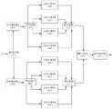
一种V频段160W固态功率合成放大器,其包括输入隔离器101、控制衰减器102、预失真模块103、驱动放大器104、固态功率放大器105、波导耦合器106、检波器107、监控单元108、电源模块109和风机110;输入隔离器101入端1脚与外部V频段入端口A连接,输入隔离器101入端2脚与控制衰减器1021脚连接;控制衰减器1032脚与预失真模块104入端1脚连接,控制衰减器102出入端3脚与监控单元108出入端3脚连接;预失真模块103出端2脚与驱动放大器104入端1脚连接;驱动放大器104出端2脚与固态功率放大器105入端1脚连接;固态功率放大器105出端2脚与波导耦合器106入端1脚连接,固态功率放大器105出端3脚与监控单元108入端4脚连接;波导耦合器106出端2脚与功放输出端口B连接,波导耦合器106出端3脚与检波器107入端1脚连接;检波器107出端2脚与监控单元108入端1脚连接;监控单元108入端2脚与电源模块109入端1脚连接,监控单元108出入端5脚与风机110出端2脚连接,监控单元108出入端6脚与功放控制端口C连接;电源模块109入端2脚与外部220V交流电源端口D连接,电源模块109出端5脚与风机110入端1脚连接,电源模块109出端3脚V+、出端4脚V-电压端与各部件相应电源端并接;A V-band 160W solid-state power synthesis amplifier, comprising aninput isolator 101, acontrol attenuator 102, apredistortion module 103, adrive amplifier 104, a solid-state power amplifier 105, awaveguide coupler 106, adetector 107, amonitoring unit 108, apower supply Module 109 andfan 110; theinput end 1 of theinput isolator 101 is connected to the external V-band input port A, theinput end 2 of theinput isolator 101 is connected to the control attenuator 1021 pin; the control attenuator 1032 pin is connected to thepredistortion module 104input Pin 1 of thecontrol attenuator 102 is connected to the input and output of thecontrol attenuator 102 andpin 3 of the input and output of themonitoring unit 108; Theinput terminal 1 of thepower amplifier 105 is connected; theoutput terminal 2 of the solid-state power amplifier 105 is connected to theinput terminal 1 of thewaveguide coupler 106;Pin 2 of the output end is connected to the output port B of the power amplifier,pin 3 of the output end of thewaveguide coupler 106 is connected to thepin 1 of the input end of thedetector 107; Theterminal 2 pin is connected to theinput terminal 1 of thepower module 109, themonitoring unit 108input terminal 5 is connected to thefan 110output terminal 2 pin, themonitoring unit 108input terminal 6 is connected to the power amplifier control port C; It is connected to external 220V AC power port D, theoutput terminal 5 of thepower module 109 is connected to thefan 110input terminal 1 pin, theoutput terminal 3 V+ of thepower module 109, and the output terminal 4 V- The voltage terminal is connected in parallel with the corresponding power terminals of each component. ;

V频段输入小信号通过外部V频段入端口A进入输入隔离器101,输入隔离器101对V频段以外的信号进行隔离衰减,减少其他信号的干扰影响,经过输入隔离后V频段信号进入控制衰减器102;控制衰减器102内数控衰减器和压控衰减器通过监控单元实现对整个链路的增益调节和控制功能,经过增益调整以后的信号进入预失真模块103;预失真模块103用于调整固态功率放大器105的幅频特性,补偿功率输出过程中引入的非线性,保证信号的线性输出,经过预失真模块103调整后的信号进入驱动放大器104;驱动放大器104对信号进行初步放大后用以驱动后面的固态功率放大器105,经过驱动放大器放大的信号进入固态功率放大器105;固态功率放大器105实现功率合成放大,达到所需要的功率输出,并将检测到的温度和电流上报给监控单元108;经过功率放大的模块进入波导耦合器106,波导耦合器106的出端口2脚将主信号传输给外部的功放输出端口B,波导耦合器106通过出端口3脚将耦合的小信号输入检波器107,检波器107将检测到的射频信号转换为直流信号输入给监控单元108,监控单元108将检波器输入的直流信号处理成输出功率显示值,监控单元108同时对固态功率放大器105的温度、电流、电源模块的控制进行处理,从而实现对整机功放的过温保护、电流检测、功率监测功能,监控单元108出端6脚与外部端口C通过串口总线连接实现外部对功放的控制,电源模块109入端4脚与外部220V交流电源端口D连接实现整机的供电,电源模块109出端4脚与风机110连接,提供风机110供电电压,电源模块109出端1脚V+、出端2脚V-电压端给各部件供电。The V-band input small signal enters theinput isolator 101 through the external V-band input port A. Theinput isolator 101 isolates and attenuates the signal outside the V-band to reduce the interference of other signals. After the input isolation, the V-band signal enters the control attenuator. 102; the numerical control attenuator and the voltage-controlled attenuator in thecontrol attenuator 102 realize the gain adjustment and control function of the entire link through the monitoring unit, and the signal after the gain adjustment enters thepredistortion module 103; thepredistortion module 103 is used to adjust the solid state The amplitude-frequency characteristic of thepower amplifier 105 compensates the nonlinearity introduced in the power output process and ensures the linear output of the signal. The signal adjusted by thepre-distortion module 103 enters thedriver amplifier 104; thedriver amplifier 104 performs preliminary amplification on the signal and then uses it to drive After the solid-state power amplifier 105, the signal amplified by the driving amplifier enters the solid-state power amplifier 105; the solid-state power amplifier 105 realizes power synthesis and amplification to achieve the required power output, and reports the detected temperature and current to themonitoring unit 108; The power amplifier module enters into thewaveguide coupler 106, theoutput port 2 of thewaveguide coupler 106 transmits the main signal to the external power amplifier output port B, and thewaveguide coupler 106 inputs the coupled small signal into thedetector 107 through theoutput port 3 pin, Thedetector 107 converts the detected radio frequency signal into a DC signal and inputs it to themonitoring unit 108. Themonitoring unit 108 processes the DC signal input by the detector into an output power display value. The control of the power supply module is processed, so as to realize the functions of over-temperature protection, current detection and power monitoring of the power amplifier of the whole machine. Theoutput terminal 6 of themonitoring unit 108 is connected to the external port C through the serial bus to realize the external control of the power amplifier. Thepower supply module 109 Theinput pin 4 is connected to the external 220V AC power port D to realize the power supply of the whole machine. Theoutput pin 4 of thepower module 109 is connected to thefan 110 to provide the power supply voltage of thefan 110. The output pin of thepower module 109 is V+ and theoutput pin 2 is V - The voltage terminal supplies power to the components.

进一步的,所述的固态功率放大器105包括魔T功分器301、波导滤波器A302、波导滤波器B303、四分路器A304、四分路器B305、功放小模块A306、功放小模块B307、功放小模块C308、功放小模块D309、功放小模块E310、功放小模块F311、功放小模块G312、功放小模块H313、四合路器A314、四合路器B315、魔T功放器316和波导滤波器C317;驱动放大器104出端2脚与魔T功分器301入端1脚连接,魔T功分器301出端2脚、3脚分别与波导滤波器A入端1脚、波导滤波器B入端1脚对应连接;波导滤波器A出端2脚与四分路器A入端1脚连接,波导滤波器B出端2脚与四分路器B入端1脚连接;四分路器A出端2脚、3脚、4脚、5脚分别与功放小模块A入端1脚、功放小模块B入端1脚、功放小模块C入端1脚、功放小模块D入端1脚一一对应连接;四分路器B出端2脚、3脚、4脚、5脚分别与功放小模块E入端1脚、功放小模块F入端1脚、功放小模块G入端1脚、功放小模块H入端1脚一一对应连接;功放小模块A出端2脚、功放小模块B出端2脚、功放小模块C出端2脚、功放小模块D出端2脚分别与四合路器A出端2脚、3脚、4脚、5脚一一对应连接;功放小模块E出端2脚、功放小模块F出端2脚、功放小模块G出端2脚、功放小模块H出端2脚分别与四合路器B出端2脚、3脚、4脚、5脚一一对应连接;四合路器A出端1脚、四合路器B出端1脚分别与魔T功放器入端2脚、3脚对应连接;魔T功放器出端1脚与波导滤波器C入端1脚连接;波导滤波器C出端2脚与波导耦合器106入端1脚连接;Further, the solid-state power amplifier 105 includes a magicT power splitter 301, a waveguide filter A302, a waveguide filter B303, a quad splitter A304, a quad splitter B305, a small power amplifier module A306, a small power amplifier module B307, Small power amplifier module C308, small power amplifier module D309, small power amplifier module E310, small power amplifier module F311, small power amplifier module G312, small power amplifier module H313, four combiner A314, four combiner B315, magicT power amplifier 316 and waveguide filter C317;pin 2 of the output end of thedrive amplifier 104 is connected to thepin 1 of the input end of the magicT power divider 301, andpins 2 and 3 of the output end of the magicT power divider 301 are respectively connected to theinput end 1 pin of the waveguide filter A, the waveguide filter Theinput terminal 1 of B is connected correspondingly; theoutput terminal 2 of the waveguide filter A is connected to theinput terminal 1 of the quad splitter A, and theoutput terminal 2 of the waveguide filter B is connected to theinput terminal 1 of the quad splitter B; The 2 pins, 3 pins, 4 pins, and 5 pins of the output terminal of the router A are respectively connected with theinput terminal 1 pin of the power amplifier module A, theinput terminal 1 pin of the power amplifier module B, theinput terminal 1 pin of the power amplifier module C, and the power amplifier module D input terminal.Pin 1 of the terminal is connected one-to-one;pins 2, 3, 4, and 5 of the output terminal of the quad splitter B are respectively connected with theinput terminal 1 of the small power amplifier module E, theinput terminal 1 of the small power amplifier module F, and the small power amplifier module G. Theinput pin 1 and theinput pin 1 of the small power amplifier module H are connected one-to-one; the output pin of the small power amplifier module A, theoutput pin 2 of the small power amplifier module B, theoutput pin 2 of the small power amplifier module C, the output pin of the small power amplifier module D The 2-pin of the terminal is respectively connected with the 2-pin, 3-pin, 4-pin and 5-pin of the four-combiner A output terminal;Pin 2 of the output end andpin 2 of the output end of the power amplifier small module H are respectively connected withpins 2, 3, 4 and 5 of the output end of the four-combiner B; Theoutput terminal 1 of the router B is connected with the magic T poweramplifier input terminal 2 and 3 correspondingly; the magic T poweramplifier output terminal 1 is connected with the waveguide filterC input terminal 1 pin; the waveguide filterC output terminal 2 feet Connect with theinput end 1 of thewaveguide coupler 106;

驱动放大器104将初步放大的V频段信号经过魔T功分器301,分成两路等幅信号分别经过波导滤波器A302、波导滤波器B303输入到四分路器A304、四分路器B305,四分路器A304将信号等分为四路等幅信号分别输入至功放小模块A306、功放小模块B307、功放小模块C308、功放小模块D309,信号经过四个功率放大器放大后通过四合路器A314进行合成输出到魔T功放器316;四分路器B305将信号等分为四路等幅信号分别输入至功放小模块E310、功放小模块F311、功放小模块G312、功放小模块H313,信号经过四个功率放大器放大后通过四合路器B315进行合成输出到魔T功放器316,魔T功放器316将信号进行合成并输出经过波导滤波器C317传输至波导耦合器106。Thedriver amplifier 104 passes the preliminary amplified V-band signal through the magicT power divider 301, and divides it into two equal-amplitude signals, respectively, through the waveguide filter A302 and the waveguide filter B303. The splitter A304 divides the signal into four equal-amplitude signals, which are respectively input to the small power amplifier module A306, the small power amplifier module B307, the small power amplifier module C308, and the small power amplifier module D309. The signal is amplified by the four power amplifiers and then passed through the four combiner A314 is synthesized and output to the magicT power amplifier 316; the quad splitter B305 divides the signal into four equal-amplitude signals and inputs them to the power amplifier small module E310, the power amplifier small module F311, the power amplifier small module G312, and the power amplifier small module H313. After being amplified by four power amplifiers, it is synthesized and output to the magicT power amplifier 316 through the quad combiner B315.

进一步的,所述的功放小模块A~H306~313的结构相同;Further, the structures of the power amplifier small modules A to H306 to 313 are the same;

每一功放小模块均包括八路功率分配器318、八路功率合成器327以及固态功放芯片A~H319~326;八路功率分配器318入端与四分路器A304出端连接,八路功率合成器327出端与四合路器A314入端连接,八路功率分配器318出端2、3、4、5、6、7、8、9脚通过波导探针过渡结构分别与固态功放芯片A~H319~326的各入端1脚一一对应连接,固态功放芯片A~H319~326的各输出端2脚通过波导探针过渡结构分别与八路功率合成器318的入端2、3、4、5、6、7、8、9脚一一对应连接,固态功放芯片A~H319~326入端3脚均通过各自的一个电阻与电压V-连接,并通过各自的另一个电阻接地,固态功放芯片A~H319~326入端4脚均与电压V+连接,固态功放芯片A319所连的电压V-处还通过一对并联电容C1、C2接地;Each small power amplifier module includes an eight-way power divider 318, an eight-way power combiner 327, and solid-state power amplifier chips A to H319 to 326; The output end is connected to the input end of the quad combiner A314, and theoutput ends 2, 3, 4, 5, 6, 7, 8, and 9 of the eight-way power divider 318 are respectively connected to the solid-state power amplifier chips A~H319~ Eachinput pin 1 of 326 is connected in a one-to-one correspondence, and eachoutput pin 2 of the solid-state power amplifier chips A~H319~326 is connected to theinput ports 2, 3, 4, 5, 5,Pins 6, 7, 8, and 9 are connected one-to-one. The solid-state power amplifier chip A~H319~326input terminal 3 pins are connected to the voltage V- through one of their respective resistors, and are grounded through the other respective resistors. The solid-state power amplifier chip A ~H319~326input terminal 4 pins are all connected with the voltage V+, and the voltage V- connected with the solid-state power amplifier chip A319 is also grounded through a pair of parallel capacitors C1 and C2;

V频段信号经过八路功率分配器318后,信号等幅地分为八份,八路功率分配器318输出的八路V频段信号分别进入第一至第八固态功率单片319~326,八路经过放大的功率信号通过八路功率合成器327进行功率合成后输出至八合路器327的输入端,固态功放芯片A~H319~326入端3脚所连的各电阻R1~R16用于实现对固态功放芯片栅极的偏置调节,固态功放芯片A319所连的并联电容C1、C2为栅极偏置电压的旁路滤波电容,电压V-和V+分别为固态功放芯片A~H319~326供电。After the V-band signal passes through the eight-way power divider 318, the signal is divided into eight equal amplitudes. The eight-way V-band signal output by the eight-way power divider 318 enters the first to eighth solid-state power monoliths 319 to 326 respectively. The power signal is combined by the eight-way power combiner 327 and then output to the input end of the eight-way combiner 327. The resistors R1 to R16 connected to the 3 pins of the solid-state power amplifier chips A to H319 to 326 are used to realize the solid-state power amplifier chip. For gate bias adjustment, the parallel capacitors C1 and C2 connected to the solid-state power amplifier chip A319 are bypass filter capacitors for the gate bias voltage, and the voltages V- and V+ supply power to the solid-state power amplifier chips A~H319~326 respectively.

本发明与背景技术相比具有以下优点:Compared with the background technology, the present invention has the following advantages:

1.本发明采用魔T功分器和四分路器结合的方式实现功率分配,同样地,采用魔T功放器和四合路器结合的方式实现功率合成,在V频段内具有低损耗、相位一致性好、输出端口间隔离度高的优点,提高了合成效率。此外,本发明中四分路器和四合路器采用基于二进制E-T结构的功率合成方式,具有低损耗、相位一致性好的优点,提高了合成效率。1. The present invention adopts the combination of magic T power splitter and quad splitter to realize power distribution, and similarly, adopts magic T power amplifier and quadruple combiner to realize power synthesis, which has low loss, The advantages of good phase consistency and high isolation between output ports improve the synthesis efficiency. In addition, the quad splitter and quad combiner in the present invention adopt the power synthesis mode based on the binary E-T structure, which has the advantages of low loss and good phase consistency, and improves the synthesis efficiency.

2. 本发明的功放小模块A采用基于波导到石英探针过渡的空间功率合成结构,使用宽带行波天线来改进系统在波传播方向的性能,每一个托盘都包含了波导到石英单探针转换结构,它采用石英单探针作为收发天线,而石英单探针过渡经过系统的优化设计后,能够保证良好的宽带性能和良好的系统输入输出端的隔离度,这些石英单探针把电磁波从波导内耦合到第一至第八固态功率单片的输入端,经过芯片放大后再把功率通过石英单探针和波导输出。该功率放大器的突出优点是通过天线辐射的方式是在完成波导-微带过渡的同时实现了八路功分,使该功率合成放大器在很小的空间内实现了八路放大,且合成效率与固态器件数量无关;采用砷化镓场效应管,具有较高的放大增益,减少了功率合成放大器之间级联的数目,这些都有利于减小功率合成放大器模块的体积和重量。2. The small power amplifier module A of the present invention adopts a spatial power synthesis structure based on the transition from waveguide to quartz probe, and uses a broadband traveling wave antenna to improve the performance of the system in the direction of wave propagation. Each tray contains a waveguide to quartz single probe. The conversion structure uses a single quartz probe as the transceiver antenna, and the single quartz probe can ensure good broadband performance and good isolation between the input and output ends of the system after the transition of the single quartz probe is optimized. The waveguide is internally coupled to the input ends of the first to eighth solid-state power monoliths, and after the chip is amplified, the power is output through the quartz single probe and the waveguide. The outstanding advantage of the power amplifier is that it realizes eight-way power division while completing the waveguide-microstrip transition by means of antenna radiation, so that the power synthesis amplifier can achieve eight-way amplification in a small space, and the synthesis efficiency is comparable to that of solid-state devices. The number is irrelevant; the use of GaAs FET has higher amplification gain and reduces the number of cascades between the power synthesis amplifiers, which are all conducive to reducing the size and weight of the power synthesis amplifier module.

3. 本发明的固态功率放大器将功放小模块A作为一个基础单元,可以将多个该模块进行统一测试,将测试结果进行排序,挑选相位、幅度一致的功放小模块进行组合,这样可以大大提高合成的功率及效率;3. The solid-state power amplifier of the present invention uses the small power amplifier module A as a basic unit, and can test multiple such modules in a unified manner, sort the test results, and select the small power amplifier modules with the same phase and amplitude for combination, which can greatly improve the performance of the power amplifier. Combined power and efficiency;

4. 本发明结构简单、各模块布局清晰明确、可维护性高、性能可靠,能够在恶劣环境(-40℃ ~ 55℃)条件下正常工作,性价比高,具有推广应用价值。4. The present invention has simple structure, clear and definite layout of each module, high maintainability, reliable performance, can work normally under harsh environment (-40°C ~ 55°C), high cost performance, and has popularization and application value.

附图说明Description of drawings

图1是本发明实施例的电原理方框图。FIG. 1 is a block diagram of an electrical principle of an embodiment of the present invention.

图2是本发明实施例中固态功率放大器的电原理方框图。FIG. 2 is a block diagram of an electrical principle of a solid-state power amplifier in an embodiment of the present invention.

图3是本发明实施例中功放小模块A的电原理方框图。FIG. 3 is a block diagram of an electrical principle of a small power amplifier module A in an embodiment of the present invention.

具体实施方式Detailed ways

下面结合附图和具体实施方式对本发明的技术方案做进一步的详细说明。The technical solutions of the present invention will be further described in detail below with reference to the accompanying drawings and specific embodiments.

参照图1~3,一种V频段160W固态功率合成放大器,其由输入隔离器101、控制衰减器102、预失真模块103、驱动放大器104、固态功率放大器105、波导耦合器106、检波器107、监控单元108、电源模块109和风机110组成。图1是本实施例的原理方框图,实施例按图1连接线路。1 to 3, a V-band 160W solid-state power synthesis amplifier is composed of aninput isolator 101, acontrol attenuator 102, apredistortion module 103, adrive amplifier 104, a solid-state power amplifier 105, awaveguide coupler 106, and adetector 107 , amonitoring unit 108 , apower supply module 109 and afan 110 . FIG. 1 is a principle block diagram of this embodiment, and the embodiment is connected to the circuit according to FIG. 1 .

本例中,输入隔离器101入端1脚通过V频段同轴电缆与外部端口A连接,实现V频段信号输入,输入隔离器101出端2脚通过V频段同轴电缆与控制衰减器102入端1脚连接,实现V频段信号输入,控制衰减器102入端3脚通过数据线与监控单元108出端3脚连接,可根据系统要求实现设备增益的步进调节,控制衰减器102入端4脚通过数据线与监控单元107出端2脚连接,监控单元108根据固态功率放大器105上报的温度信息进行综合处理,使系统在温度变化时增益波动控制在较小范围内,控制衰减器102的出端2脚通过V频段同轴电缆输出到预失真模块103入端1脚,预失真模块103对信号进行预失真校准,调整信号的幅频特性,改善系统信号的线性度,预失真模块103的出端2脚通过V频段弯波导输出到驱动放大器104入端1脚,驱动放大器104对信号进行初步放大,驱动放大器104出端2将初步放大的信号传输到固态功率放大器105入端1脚,固态功率放大器105将64路芯片进行功率合成后输出,固态功率放大器105将其温度和电流通过DS18B20及MAX4173TEUT芯片上报给监控单元108,固态功率放大器105将合成后的功率信号传输给波导耦合器106入端1脚,主路功率信号通过波导耦合器106出端2脚传输给外部波导口B,波导耦合器106通过波导内探针耦合的方式通过出端口3脚将耦合的小信号输入检波器107入端1脚,检波器107的出端2脚将检测到的射频信号转换为直流信号输入给监控单元108入端1脚,监控单元108将检波器107输入的直流信号处理成输出功率显示值,监控单元108同时对固态功放模块105上报的温度、电流、进行处理,从而实现对整机功放的过温保护、电流检测、功率监测等功能,监控单元108出端6脚与外部端口C通过串口总线连接实现外部对功放的控制,波导耦合器106采用市售CP47-51GW-2730制作,检波器107采用市售W55-001C50G25B制作。电源模块109提供各级部件直流工作电压,采用市售型号为SFM3880-220Q24C1的开关电源,其输出V+电压为+24伏、输出V-电压为-5伏,电源模块109入端3脚可接受监控单元108的控制,在非正常情况下关断输出电压,实现自我保护功能,风机110采用市售9WV0848P1H001型结构,电源模块109为其提供+48V供电电压。In this example, theinput pin 1 of theinput isolator 101 is connected to the external port A through the V-band coaxial cable to realize the V-band signal input, and theoutput end 2 of theinput isolator 101 is connected to thecontrol attenuator 102 through the V-band coaxial cable. Theterminal 1 is connected to realize the V-band signal input, and theinput terminal 3 of thecontrol attenuator 102 is connected to theoutput terminal 3 of themonitoring unit 108 through the data cable. The step adjustment of the equipment gain can be realized according to the system requirements, and the input terminal of theattenuator 102 can be controlled.Pin 4 is connected to pin 2 of the output end of themonitoring unit 107 through a data cable. Themonitoring unit 108 performs comprehensive processing according to the temperature information reported by the solid-state power amplifier 105, so that the gain fluctuation of the system is controlled within a small range when the temperature changes, and theattenuator 102 is controlled. Theoutput pin 2 is output to theinput pin 1 of thepre-distortion module 103 through the V-band coaxial cable. Thepre-distortion module 103 performs pre-distortion calibration on the signal, adjusts the amplitude-frequency characteristics of the signal, and improves the linearity of the system signal. The pre-distortion module Theoutput pin 2 of 103 is output to theinput pin 1 of thedrive amplifier 104 through the V-band curved waveguide. Thedrive amplifier 104 initially amplifies the signal, and theoutput end 2 of thedrive amplifier 104 transmits the preliminary amplified signal to the solid-state power amplifier 105 Theinput end 1 The solid-state power amplifier 105 synthesizes the power of the 64-channel chips and outputs it. The solid-state power amplifier 105 reports its temperature and current to themonitoring unit 108 through the DS18B20 and MAX4173TEUT chips. The solid-state power amplifier 105 transmits the synthesized power signal to the waveguide coupling. Theinput pin 1 of thecoupler 106, the main circuit power signal is transmitted to the external waveguide port B through theoutput pin 2 of thewaveguide coupler 106, and thewaveguide coupler 106 inputs the coupled small signal through theoutput port 3 pin by means of probe coupling in the waveguide. Theinput pin 1 of thedetector 107 and theoutput pin 2 of thedetector 107 convert the detected radio frequency signal into a DC signal and input it to theinput pin 1 of themonitoring unit 108. Themonitoring unit 108 processes the DC signal input by thedetector 107 into an output The power display value, themonitoring unit 108 simultaneously processes the temperature and current reported by the solid-statepower amplifier module 105, so as to realize the functions of over-temperature protection, current detection, and power monitoring of the power amplifier of the whole machine. Port C is connected through a serial bus to realize external control of the power amplifier. Thewaveguide coupler 106 is made of commercially available CP47-51GW-2730, and thedetector 107 is made of commercially available W55-001C50G25B. Thepower supply module 109 provides the DC working voltage of the components at all levels, and adopts the commercially available switching power supply model SFM3880-220Q24C1. The output V+ voltage is +24 volts, and the output V- voltage is -5 volts. Theinput terminal 3 of thepower supply module 109 can be monitored and controlled. The control of theunit 108 turns off the output voltage under abnormal conditions to realize the self-protection function. Thefan 110 adopts a commercially available 9WV0848P1H001 structure, and thepower module 109 provides +48V supply voltage for it.

预失真模块与驱动放大器104由小信号放大器、驱动放大器组成,实施例采用HMC1144和NC116210C-4651P5制作。所述的固态功率放大器104由魔T功分器301、波导滤波器A302、波导滤波器B303、四分路器A304、四分路器B305、功放小模块A306、功放小模块B307、功放小模块C308、功放小模块D309、功放小模块E310、功放小模块F311、功放小模块G312、功放小模块H313、四合路器A314、四合路器B315、魔T功放器316、波导滤波器C317组成,四分路器A304和四分路器B305、四合路器A314、四合路器B315结构完全一致,采用基于波导E-T结的二进制空间合成结构;The predistortion module and thedriver amplifier 104 are composed of a small signal amplifier and a driver amplifier. The embodiment is made of HMC1144 and NC116210C-4651P5. The solid-state power amplifier 104 is composed of a magicT power splitter 301, a waveguide filter A302, a waveguide filter B303, a quad splitter A304, a quad splitter B305, a small power amplifier module A306, a small power amplifier module B307, and a small power amplifier module. C308, small power amplifier module D309, small power amplifier module E310, small power amplifier module F311, small power amplifier module G312, small power amplifier module H313, four combiner A314, four combiner B315, magicT power amplifier 316, waveguide filter C317 , The structure of the quad splitter A304 and the quad splitter B305, the quadruple combiner A314 and the quadruple combiner B315 are exactly the same, and the binary space synthesis structure based on the waveguide E-T junction is adopted;

魔T功分器301出端2脚、3脚分别与波导滤波器A302入端1脚、波导滤波器B303入端1脚对应连接;波导滤波器A302出端2脚、波导滤波器B303出端2脚分别与四分路器A304入端1脚、四分路器B305入端1脚连接;四分路器A304出端2脚、3脚、4脚、5脚分别与功放小模块A306入端1脚、功放小模块B307入端1脚、功放小模块C308入端1脚、功放小模块D309入端1脚一一对应连接;四分路器B305出端2脚、3脚、4脚、5脚分别与功放小模块E310入端1脚、功放小模块F311入端1脚、功放小模块G312入端1脚、功放小模块H313入端1脚一一对应连接;功放小模块A306出端2脚、功放小模块B307出端2脚、功放小模块C308出端2脚、功放小模块D309出端2脚分别与四合路器A314出端2脚、3脚、4脚、5脚一一对应连接;功放小模块E310出端2脚、功放小模块F311出端2脚、功放小模块G312出端2脚、功放小模块H313出端2脚分别与四合路器B315出端2脚、3脚、4脚、5脚一一对应连接;四合路器A314出端1脚、四合路器B315出端1脚分别与魔T功放器316入端2脚、3脚对应连接;魔T功放器316出端1脚与波导滤波器C317入端1脚连接;波导滤波器C317出端2脚与波导耦合器入端1脚连接;功放小模块A-H八个模块结构功能完全相同。MagicT power splitter 301output pin 2 and 3 are respectively connected with waveguide filterA302 input pin 1 and waveguide filterB303 input pin 1 correspondingly; waveguide filterA302 output pin 2, waveguide filter B303 output pin The 2 pins are respectively connected with theinput pin 1 of the quad splitter A304 and theinput pin 1 of the quad splitter B305; Theterminal 1 pin, the power amplifier small moduleB307 input terminal 1 pin, the power amplifier small moduleC308 input terminal 1 pin, the power amplifier small moduleD309 input terminal 1 pin are connected one by one; the four splitterB305 output terminal 2 feet, 3 feet, 4 feet , 5 pins are respectively connected with theinput pin 1 of the power amplifier small module E310, theinput pin 1 of the power amplifier small module F311, theinput pin 1 of the power amplifier small module G312, and theinput pin 1 of the power amplifier small module H313.Pin 2 of the terminal,pin 2 of the output of the small power amplifier module B307,pin 2 of the output of the small power amplifier module C308,pin 2 of the output of the small power amplifier module D309, andpin 2,pin 3,pin 4, andpin 5 of the four combiner A314 respectively One-to-one connection; 2 feet of the output of the small power amplifier module E310, 2 feet of the output of the small power amplifier module F311, 2 feet of the output of the small power amplifier module G312, 2 feet of the output of the small power amplifier module H313, and 2 feet of the output of the four combiner B315 Pin,pin 3,pin 4,pin 5 are connected one by one;pin 1 of the output end of the four-combiner A314,pin 1 of the output end of the four-combiner B315 are respectively connected to thepin 2 andpin 3 of the input end of the magicT power amplifier 316. ;MagicT power amplifier 316output terminal 1 is connected with waveguide filterC317 input terminal 1 pin; waveguide filterC317 output terminal 2 feet are connected with waveguidecoupler input terminal 1 pin; power amplifier small modules A-H eight modules have the same structure and function .

功放小模块A306由八路功率分配器、八路功率合成器、第一至第八固态功率单片、第一至第十六电阻、电容C1、电容C2组成;八路功率分配器入端与八分路器出端连接,八路功率分配器出端与八合路器入端连接,八路功率分配器出端2、3、4、5、6、7、8通过波导石英探针过渡分别与第一至第八固态功率单片的各入端1一一对应连接,第一至第八固态功率单片的各输出端2通过波导石英探针过渡分别与八路功率合成器的入端2、3、4、5、6、7、8、9一一对应;V频段信号经过八路功率分配器后,信号等幅地分为八份,八路功率分配器输出的八路V频段信号分别进入第一至第八固态功率单片,八路经过放大的功率信号通过八路功率合成器进行功率合成后输出至八合路器的输入端,第一至第八固态功率单片入端4脚与电压V+连接第一至第十六电阻R1至R16、用于实现对第一至第八固态功率单片栅极的偏置调节,电容C1,电容C2是栅极偏置电压的旁路滤波电容,电压V+分别对第一至第八固态功率单片供电。实施例和功放盒体一起用铝合金进行加工,表面镀镍金。功率单片(319至326)采用相同的电路结构形式,各路放大器的入端3脚分别通过相同的分压电阻获得负压输入,入端4脚均与模块电源107输出+7V电压连接,各路放大器的作用均是提供功率增益,获得单管电路的最大输出功率,实施例每个功率单片各采用一只市售NC116210C-4651P5制作。The small power amplifier module A306 consists of an eight-way power divider, an eight-way power combiner, the first to eighth solid-state power monoliths, the first to sixteenth resistors, a capacitor C1, and a capacitor C2; the input end of the eight-way power divider and the eight-way shunt The output end of the eight-way power divider is connected to the input end of the eight-way power divider. The input ends 1 of the eighth solid-state power monolith are connected in a one-to-one correspondence, and the output ends 2 of the first to eighth solid-state power monoliths are respectively connected to the input ends 2, 3, and 4 of the eight-way power combiner through a waveguide quartz probe transition. , 5, 6, 7, 8, and 9 are in one-to-one correspondence; after the V-band signal passes through the eight-way power divider, the signal is divided into eight equal amplitudes, and the eight-way V-band signal output by the eight-way power divider enters the first to eighth respectively. Solid-state power monolithic, the eight-channel amplified power signals are combined by the eight-channel power combiner and then output to the input end of the eight-way combiner. The first to eighth solid-state power single-chip input terminals 4 are connected to the voltage V+. The first to The sixteenth resistors R1 to R16 are used to adjust the bias of the first to eighth solid-state power monolithic gates. The capacitors C1 and C2 are bypass filter capacitors for the gate bias voltage. One to eighth solid state power monolithic power supply. The embodiment and the power amplifier box are processed with aluminum alloy, and the surface is plated with nickel and gold. The power single chip (319 to 326) adopts the same circuit structure. Theinput terminal 3 of each amplifier obtains the negative voltage input through the same voltage divider resistor, and theinput terminal 4 is connected to themodule power supply 107 output +7V voltage. The function of each amplifier is to provide power gain and obtain the maximum output power of the single-tube circuit. In the embodiment, each power single-chip is made of a commercially available NC116210C-4651P5.

上述固态功率合成放大器的简要工作原理如下:The brief working principle of the above solid-state power synthesis amplifier is as follows:

V频段160W固态功率合成放大器由输入隔离器101、控制衰减器102、预失真模块103、驱动放大器104、固态功率放大器105、波导耦合器106、检波器107、监控单元108、电源模块109和风机110组成。V频段输入小信号首先进入输入隔离器101再输出至控制衰减器102,通过监控单元108控制实现整机的增益步进调节和对整机增益波动调节。经过增益调整以后的信号进入预失真模块;预失真模块对信号进行线性化调整后输出到驱动放大器;驱动放大器对信号进行初步放大,经过驱动放大器放大的信号进入固态功率放大器,固态功率放大器实现功率合成放大,达到所需要的功率输出,并将检测到的温度和电流上报给监控单元;经过功率放大的模块进入波导耦合器,波导耦合器的将主信号传输给外部波导口B,波导耦合器将耦合的小信号输入检波器,检波器将检测到的射频信号转换为直流信号输入给监控单元。The V-band 160W solid-state power synthesis amplifier consists of aninput isolator 101, acontrol attenuator 102, apredistortion module 103, adrive amplifier 104, a solid-state power amplifier 105, awaveguide coupler 106, adetector 107, amonitoring unit 108, apower module 109 and afan 110 compositions. The V-band input small signal first enters theinput isolator 101 and then is output to thecontrol attenuator 102, and is controlled by themonitoring unit 108 to realize the step adjustment of the gain of the whole machine and the adjustment of the gain fluctuation of the whole machine. The signal after gain adjustment enters the pre-distortion module; the pre-distortion module linearizes the signal and outputs it to the driver amplifier; the driver amplifier initially amplifies the signal, and the signal amplified by the driver amplifier enters the solid-state power amplifier, and the solid-state power amplifier realizes power Synthesize amplification to achieve the required power output, and report the detected temperature and current to the monitoring unit; the power amplified module enters the waveguide coupler, and the waveguide coupler transmits the main signal to the external waveguide port B, the waveguide coupler The coupled small signal is input to the detector, and the detector converts the detected radio frequency signal into a DC signal and inputs it to the monitoring unit.

上述固态功率合成放大器的安装结构如下:The installation structure of the above solid-state power synthesis amplifier is as follows:

把图1中输入隔离器101、控制衰减器102、预失真模块103、驱动放大器104、固态功率放大器105、波导耦合器106、检波器107、监控单元108和电源109共同安装在一个长×宽×高为3450毫米×335毫米×145毫米的密闭机箱内,风机110安装在机箱底部散热翅片上,V频段信号在不同部件之间的传输通过同轴射频电缆和V频段波导连接,控制信号通过软导线与监控单元连接,机箱加工采用屏蔽结构,可实现电磁信号的空间隔离,组装成本发明。Theinput isolator 101, thecontrol attenuator 102, thepredistortion module 103, thedrive amplifier 104, the solid-state power amplifier 105, thewaveguide coupler 106, thedetector 107, themonitoring unit 108 and thepower supply 109 in FIG. 1 are installed together in a length × width In an airtight case with a height of 3450 mm×335 mm×145 mm, thefan 110 is installed on the cooling fins at the bottom of the case. The transmission of V-band signals between different components is connected through coaxial RF cables and V-band waveguides, and the control signals pass through The flexible wire is connected with the monitoring unit, and the case processing adopts a shielding structure, which can realize the spatial isolation of electromagnetic signals, and is assembled in the present invention.

总之,本发明采用了一种波导内空间64路功率合成方式,基于波导探针过渡结构将八个功率芯片进行合成,构成一个功放小模块,再采用四路波导E-T型结构的二进制功率分配/合成网络将四个功放小模块进行合成,最后采用魔T结构的功率分配/合成网络将信号合成达到160W的功率输出。该功率放大器在V频段将64路功率芯片进行合成,具有合成效率高、频率高、重量轻、体积小、集成化程度高、性能稳定可靠、易维护、工作温度范围宽(-40℃~55℃)等特点,特别适用于卫星通信微波信道的功率放大业务。In a word, the present invention adopts a 64-channel power synthesis method in the inner space of the waveguide. Based on the transition structure of the waveguide probe, eight power chips are synthesized to form a small power amplifier module, and then the binary power distribution / The synthesis network synthesizes the four small power amplifier modules, and finally adopts the power distribution/synthesis network of the magic T structure to synthesize the signal to achieve a power output of 160W. The power amplifier synthesizes 64 power chips in the V frequency band, and has the advantages of high synthesis efficiency, high frequency, light weight, small size, high integration degree, stable and reliable performance, easy maintenance, and wide operating temperature range (-40℃~55℃). ℃) and other characteristics, especially suitable for the power amplification business of satellite communication microwave channel.

Claims (3)

1. A V-band 160W solid-state power synthesis amplifier is characterized by comprising an input isolator (101), a control attenuator (102), a predistortion module (103), a drive amplifier (104), a solid-state power amplifier (105), a waveguide coupler (106), a detector (107), a monitoring unit (108), a power supply module (109) and a fan (110); the pin 1 at the input end of the input isolator (101) is connected with the external V-band input port (A), and the pin 2 at the output end of the input isolator (101) is connected with the pin 1 of the control attenuator (102); a pin 2 of the control attenuator (103) is connected with a pin 1 at the input end of the predistortion module (104), and a pin 3 at the input end of the control attenuator (102) is connected with a pin 3 at the output end of the monitoring unit (108); a pin 2 at the output end of the predistortion module (103) is connected with a pin 1 at the input end of the drive amplifier (104); the pin 2 at the output end of the drive amplifier (104) is connected with the pin 1 at the input end of the solid-state power amplifier (105); a pin 2 at the output end of the solid-state power amplifier (105) is connected with a pin 1 at the input end of the waveguide coupler (106), and a pin 3 at the output end of the solid-state power amplifier (105) is connected with a pin 4 at the input end of the monitoring unit (108); a pin 2 at the output end of the waveguide coupler (106) is connected with the power amplifier output port (B), and a pin 3 at the output end of the waveguide coupler (106) is connected with a pin 1 at the input end of the detector (107); a pin 2 at the output end of the detector (107) is connected with a pin 1 at the input end of the monitoring unit (108); a pin 2 at the output end of the monitoring unit (108) is connected with a pin 1 at the input end of the power module (109), a pin 5 at the input end of the monitoring unit (108) is connected with a pin 2 at the output end of the fan (110), and a pin 6 at the output end of the monitoring unit (108) is connected with a power amplifier control port (C); 2 pins at the input end of the power module (109) are connected with an external 220V alternating current power supply port (D), 5 pins at the output end of the power module (109) are connected with 1 pin at the input end of the fan (110), and 3 pins V + at the output end of the power module (109) and 4 pins V-voltage end at the output end of the power module (109) are connected with corresponding power supply ends of all components in parallel;
small input signals in the V frequency range enter an input isolator (101) through an external V frequency range input port (A), the input isolator (101) isolates and attenuates signals outside the V frequency range, interference influence of other signals is reduced, and the V frequency range signals enter a control attenuator (102) after input isolation; the numerical control attenuator and the voltage-controlled attenuator in the control attenuator (102) realize the gain adjustment and control functions of the whole link through a monitoring unit, and signals after gain adjustment enter a predistortion module (103); the predistortion module (103) is used for adjusting the amplitude-frequency characteristic of the solid-state power amplifier (105), compensating nonlinearity introduced in the power output process, ensuring the linear output of signals, and enabling the signals adjusted by the predistortion module (103) to enter the drive amplifier (104); the driving amplifier (104) is used for driving a subsequent solid-state power amplifier (105) after preliminarily amplifying the signal, and the signal amplified by the driving amplifier enters the solid-state power amplifier (105); the solid-state power amplifier (105) realizes power synthesis and amplification, achieves required power output, and reports the detected temperature and current to the monitoring unit (108); the power amplified module enters a waveguide coupler (106), a main signal is transmitted to an external power amplifier output port (B) by an output end 2 pin of the waveguide coupler (106), a coupled small signal is input into a detector (107) by an output end 3 pin of the waveguide coupler (106), the detector (107) converts a detected radio frequency signal into a direct current signal and inputs the direct current signal to a monitoring unit (108), the monitoring unit (108) processes the direct current signal input by the detector into an output power display value, the monitoring unit (108) simultaneously processes the temperature, the current and the control of a power supply module of a solid-state power amplifier (105), thereby realizing the functions of over-temperature protection, current detection and power monitoring of the power amplifier of the whole machine, the output end 6 pin of the monitoring unit (108) is connected with the power amplifier control port (C) through a serial port bus to realize the external control of the power amplifier, the input end 2 pin of the power supply module (109) is connected with an external 220V alternating current port (D) to realize the power supply of the whole machine, 5 pins of the output end of the power module (109) are connected with the fan (110) to provide power supply voltage for the fan (110), and 3 pin V + of the output end of the power module (109) and 4 pin V-voltage end of the output end of the power module (109) supply power for each component.
2. The V-band 160W solid-state power synthesis amplifier according to claim 1, wherein the solid-state power amplifier (105) comprises a magic T power divider (301), a waveguide filter A (302), a waveguide filter B (303), a four-way divider A (304), a four-way divider B (305), a small power amplifier module A (306), a small power amplifier module B (307), a small power amplifier module C (308), a small power amplifier module D (309), a small power amplifier module E (310), a small power amplifier module F (311), a small power amplifier module G (312), a small power amplifier module H (313), a four-way combiner A (314), a four-way combiner B (315), a magic T power amplifier (316) and a waveguide filter C (317); a pin 2 at the output end of the drive amplifier (104) is connected with a pin 1 at the input end of the magic T power divider (301), and a pin 2 and a pin 3 at the output end of the magic T power divider (301) are respectively and correspondingly connected with a pin 1 at the input end of the waveguide filter A and a pin 1 at the input end of the waveguide filter B; the pin 2 at the output end of the waveguide filter A is connected with the pin 1 at the input end of the four-shunt device A, and the pin 2 at the output end of the waveguide filter B is connected with the pin 1 at the input end of the four-shunt device B; the 2 pins, the 3 pins, the 4 pins and the 5 pins of the output end of the four-branching device A are respectively connected with the 1 pin of the input end of the small power amplifier module A, the 1 pin of the input end of the small power amplifier module B, the 1 pin of the input end of the small power amplifier module C and the 1 pin of the input end of the small power amplifier module D in a one-to-one correspondence manner; the 2 pins, the 3 pins, the 4 pins and the 5 pins of the output end of the four-branching device B are respectively connected with the 1 pin of the input end of the small power amplifier module E, the 1 pin of the input end of the small power amplifier module F, the 1 pin of the input end of the small power amplifier module G and the 1 pin of the input end of the small power amplifier module H in a one-to-one correspondence manner; the output end 2 pin of the small power amplifier module A, the output end 2 pin of the small power amplifier module B, the output end 2 pin of the small power amplifier module C and the output end 2 pin of the small power amplifier module D are respectively connected with the output ends 2 pin, 3 pin, 4 pin and 5 pin of the four combiner A in a one-to-one correspondence manner; the output end 2 pin of the small power amplifier module E, the output end 2 pin of the small power amplifier module F, the output end 2 pin of the small power amplifier module G and the output end 2 pin of the small power amplifier module H are respectively connected with the output ends 2 pin, 3 pin, 4 pin and 5 pin of the four combiner B in a one-to-one correspondence manner; the pin 1 of the output end of the four combiner A and the pin 1 of the output end of the four combiner B are respectively and correspondingly connected with the pin 2 and the pin 3 of the input end of the magic T power amplifier; the output end 1 pin of the magic T power amplifier is connected with the input end 1 pin of the waveguide filter C; the pin 2 at the output end of the waveguide filter C is connected with the pin 1 at the input end of the waveguide coupler (106);
the drive amplifier (104) divides the preliminarily amplified V-band signal into two paths of equal amplitude signals through a magic T power divider (301), the two paths of equal amplitude signals are respectively input into a four-way splitter A (304) and a four-way splitter B (305) through a waveguide filter A (302) and a waveguide filter B (303), the four-way splitter A (304) equally divides the signal into four paths of equal amplitude signals which are respectively input into a small power amplifier module A (306), a small power amplifier module B (307), a small power amplifier module C (308) and a small power amplifier module D (309), and the signal is amplified by four power amplifiers and then synthesized through a four-way splitter A (314) and output to a magic T power amplifier (316); the four-way splitter B (305) equally divides signals into four paths of equiamplitude signals which are respectively input to the small power amplifier module E (310), the small power amplifier module F (311), the small power amplifier module G (312) and the small power amplifier module H (313), the signals are amplified by the four power amplifiers and then synthesized by the four-way combiner B (315) and output to the magic T power amplifier (316), and the magic T power amplifier (316) synthesizes the signals and outputs the signals to the waveguide coupler (106) through the waveguide filter C (317).
each power amplifier small module comprises an eight-path power distributor (318), an eight-path power synthesizer (327) and solid power amplifier chips A-H (319-326); the input end of an eight-path power divider (318) is connected with the output end of a four-way combiner A (304), the output end of an eight-path power combiner (327) is connected with the input end of a four-way combiner A (314), the output ends 2, 3, 4, 5, 6, 7, 8 and 9 of the eight-path power divider (318) are respectively connected with the input ends 1 of solid power amplifier chips A-H (319-326) in a one-to-one correspondence manner through waveguide probe transition structures, the output ends 2 of the solid power amplifier chips A-H (319-326) are respectively connected with the input ends 2, 3, 4, 5, 6, 7, 8 and 9 of the eight-path power combiner (318) in a one-to-one correspondence manner through waveguide probe transition structures, the input ends 3 of the solid power amplifier chips A-H (319-326) are respectively connected with a voltage V-through respective resistor and grounded through respective other resistor, and the input ends 4 of the solid power amplifier chips A-H (319-326) are respectively connected with a voltage V + 326, the voltage V-position connected with the solid-state power amplifier chip A (319) is also grounded through a pair of parallel capacitors (C1 and C2);
after a V-band signal passes through an eight-path power divider (318), the signal is divided into eight parts in an equal amplitude manner, eight paths of V-band signals output by the eight-path power divider (318) respectively enter a first solid-state power single chip (319) to an eighth solid-state power single chip (326) to an eighth solid-state power single chip, eight paths of amplified power signals are subjected to power synthesis through an eight-path power synthesizer (327) and then are output to the input end of the eight-path synthesizer (327), resistors (R1-R16) connected to pins 3 at the input end of a solid-state power amplifier chip A (319) to H (319-326) are used for realizing bias adjustment of a grid electrode of the solid-state power amplifier chip, parallel capacitors (C1 and C2) connected to the solid-state power amplifier chip A (319) are bypass filter capacitors of grid bias voltage, and voltages V & lt + & gt are used for supplying power to the solid-state power amplifier chips A (319-H (319-326) respectively.
CN202011296741.0A2020-11-182020-11-18 A V-band 160W solid-state power synthesis amplifierActiveCN112491373B (en)

Priority Applications (1)

Application NumberPriority DateFiling DateTitle
CN202011296741.0ACN112491373B (en)2020-11-182020-11-18 A V-band 160W solid-state power synthesis amplifier

Applications Claiming Priority (1)

Application NumberPriority DateFiling DateTitle
CN202011296741.0ACN112491373B (en)2020-11-182020-11-18 A V-band 160W solid-state power synthesis amplifier

Publications (2)

Publication NumberPublication Date
CN112491373A CN112491373A (en)2021-03-12
CN112491373Btrue CN112491373B (en)2022-08-12

Family

ID=74931589

Family Applications (1)

Application NumberTitlePriority DateFiling Date
CN202011296741.0AActiveCN112491373B (en)2020-11-182020-11-18 A V-band 160W solid-state power synthesis amplifier

Country Status (1)

CountryLink
CN (1)CN112491373B (en)

Families Citing this family (3)

* Cited by examiner, † Cited by third party
Publication numberPriority datePublication dateAssigneeTitle
CN113702916A (en)*2021-06-242021-11-26北京无线电测量研究所Compact 2-18GHz solid-state ultra-wideband transmitter
CN115242200B (en)*2022-09-152023-01-06成都国盛军通科技有限公司 A C-band radio frequency signal power amplification device and method
CN120185643B (en)*2025-05-232025-08-12武汉嘉瑞科技有限公司 A power amplifier combiner

Citations (5)

* Cited by examiner, † Cited by third party
Publication numberPriority datePublication dateAssigneeTitle
CN102355207A (en)*2011-09-292012-02-15中国电子科技集团公司第五十四研究所Ka frequency-band solid-state power amplifier
CN105306132A (en)*2015-11-182016-02-03南京中网卫星通信股份有限公司Close-loop control portable station with automatic monitoring function
CN105356928A (en)*2015-09-282016-02-24四川九洲电器集团有限责任公司Satellite communication frequency conversion terminal equipment of Ku band
US10374852B1 (en)*2018-09-102019-08-06United States Of America As Represented By The Administrator Of NasaKa-band modulator and transmitter
CN210578441U (en)*2019-12-202020-05-19成都菲斯洛克电子技术有限公司Novel Ka frequency band solid-state power amplifier

Family Cites Families (2)

* Cited by examiner, † Cited by third party
Publication numberPriority datePublication dateAssigneeTitle
WO2009033155A1 (en)*2007-09-062009-03-12Vt Idirect, Inc.Highly integrated very small aperture terminal (vsat) apparatus and method
US10218325B2 (en)*2016-04-272019-02-26California Institute Of TechnologySpatial power combining mechanism (SPCM) for the generation and amplification of electromagnetic radiation

Patent Citations (5)

* Cited by examiner, † Cited by third party
Publication numberPriority datePublication dateAssigneeTitle
CN102355207A (en)*2011-09-292012-02-15中国电子科技集团公司第五十四研究所Ka frequency-band solid-state power amplifier
CN105356928A (en)*2015-09-282016-02-24四川九洲电器集团有限责任公司Satellite communication frequency conversion terminal equipment of Ku band
CN105306132A (en)*2015-11-182016-02-03南京中网卫星通信股份有限公司Close-loop control portable station with automatic monitoring function
US10374852B1 (en)*2018-09-102019-08-06United States Of America As Represented By The Administrator Of NasaKa-band modulator and transmitter
CN210578441U (en)*2019-12-202020-05-19成都菲斯洛克电子技术有限公司Novel Ka frequency band solid-state power amplifier

Non-Patent Citations (3)

* Cited by examiner, † Cited by third party
Title
A C-band 1KW Power Amplifier Design Based on Waveguide Magic T Synthesis;Xiaobing Kou;《2020 International Conference on Microwave and Millimeter Wave Technology (ICMMT)》;20200323;全文*
室内型Ku频段150W功率放大器设计;刘立浩等;《无线电工程》;20200303(第03期);全文*
小型化高功率微波功率放大器的实现;张东;《电子技术与软件工程》;20200501;全文*

Also Published As

Publication numberPublication date
CN112491373A (en)2021-03-12

Similar Documents

PublicationPublication DateTitle
CN112491373B (en) A V-band 160W solid-state power synthesis amplifier
CN206993063U (en)A kind of Ku frequency ranges solid-state power combination amplifier
CN102355207B (en)Ka frequency-band solid-state power amplifier
CN114421978B (en)Ultra-wideband high-power high-efficiency multi-band transmitting subsystem
CN107248848A (en)A kind of EHF frequency ranges High Linear solid-state high power amplifier device
CN108448219A (en)A kind of E wave bands waveguide E-T branches and multiprobe coupled structure power synthesis amplifier
CN216252696U (en)Ultra-wideband high-power high-efficiency multiband transmission subsystem
CN213879769U (en)High-power hybrid synthetic circuit of multi-module X-band solid-state transmitter
Li et al.A 110-to-130GHz SiGe BiCMOS Doherty power amplifier with slotline-based power-combining technique achieving> 22dBm saturated output power and> 10% power back-off efficiency
CN102868368A (en)Double-frequency synchronous power amplifier based on T-type network and coupling line and design method thereof
CN101834571A (en)Efficient linear power amplifier circuit
CN110739922A (en)ultra-wideband solid-state power amplifier synthesis circuit
CN202424626U (en)Multichannel asymmetric Doherty amplifier
Xie et al.Design and analysis of Ka-band power amplifier with sandwiched-coupler-balun and folded-T-line power combiner
WO2025148642A1 (en)Digital predistortion circuit and antenna device
CN111082817A (en)Phase compensation method and system for improving linearity
CN101414875B (en) Method, device and system for covering tunnel in time division duplex system
CN104270104A (en)High-intermodulation power amplifier employing APD (Amplitude Probability Distribution) technology
CN105680801B (en)A kind of multimode power amplifier and its mobile terminal for balancing heat dissipation
CN216904826U (en)Ku frequency band power amplifier module
CN206524816U (en)It is a kind of to be used for the power amplifier of 2~6GHz frequency ranges
CN208208950U (en)A kind of E wave band waveguide E-T branch and multiprobe coupled structure power synthesis amplifier
CN108900207B (en)Power amplifier device, radio frequency signal processing system and base station
CN203288755U (en)RoF-type phase control active integrated antenna array suitable for FDD system
CN120811300A (en)V-band 100W solid-state power synthesis amplifier

Legal Events

DateCodeTitleDescription
PB01Publication
PB01Publication
SE01Entry into force of request for substantive examination
GR01Patent grant
GR01Patent grant

[8]ページ先頭

©2009-2025 Movatter.jp