CN112470062B - Switchable light-collimating layers comprising bistable electrophoretic fluids - Google Patents
Switchable light-collimating layers comprising bistable electrophoretic fluidsDownload PDFInfo
- Publication number
- CN112470062B CN112470062BCN201980048552.0ACN201980048552ACN112470062BCN 112470062 BCN112470062 BCN 112470062BCN 201980048552 ACN201980048552 ACN 201980048552ACN 112470062 BCN112470062 BCN 112470062B
- Authority
- CN
- China
- Prior art keywords
- light
- layer
- elongated
- collimating
- row
- Prior art date
- Legal status (The legal status is an assumption and is not a legal conclusion. Google has not performed a legal analysis and makes no representation as to the accuracy of the status listed.)
- Active
Links
Images


Classifications
- G—PHYSICS
- G02—OPTICS
- G02F—OPTICAL DEVICES OR ARRANGEMENTS FOR THE CONTROL OF LIGHT BY MODIFICATION OF THE OPTICAL PROPERTIES OF THE MEDIA OF THE ELEMENTS INVOLVED THEREIN; NON-LINEAR OPTICS; FREQUENCY-CHANGING OF LIGHT; OPTICAL LOGIC ELEMENTS; OPTICAL ANALOGUE/DIGITAL CONVERTERS
- G02F1/00—Devices or arrangements for the control of the intensity, colour, phase, polarisation or direction of light arriving from an independent light source, e.g. switching, gating or modulating; Non-linear optics
- G02F1/01—Devices or arrangements for the control of the intensity, colour, phase, polarisation or direction of light arriving from an independent light source, e.g. switching, gating or modulating; Non-linear optics for the control of the intensity, phase, polarisation or colour
- G02F1/165—Devices or arrangements for the control of the intensity, colour, phase, polarisation or direction of light arriving from an independent light source, e.g. switching, gating or modulating; Non-linear optics for the control of the intensity, phase, polarisation or colour based on translational movement of particles in a fluid under the influence of an applied field
- G02F1/1675—Constructional details
- G—PHYSICS
- G02—OPTICS
- G02B—OPTICAL ELEMENTS, SYSTEMS OR APPARATUS
- G02B27/00—Optical systems or apparatus not provided for by any of the groups G02B1/00 - G02B26/00, G02B30/00
- G02B27/30—Collimators
- G—PHYSICS
- G02—OPTICS
- G02F—OPTICAL DEVICES OR ARRANGEMENTS FOR THE CONTROL OF LIGHT BY MODIFICATION OF THE OPTICAL PROPERTIES OF THE MEDIA OF THE ELEMENTS INVOLVED THEREIN; NON-LINEAR OPTICS; FREQUENCY-CHANGING OF LIGHT; OPTICAL LOGIC ELEMENTS; OPTICAL ANALOGUE/DIGITAL CONVERTERS
- G02F1/00—Devices or arrangements for the control of the intensity, colour, phase, polarisation or direction of light arriving from an independent light source, e.g. switching, gating or modulating; Non-linear optics
- G02F1/29—Devices or arrangements for the control of the intensity, colour, phase, polarisation or direction of light arriving from an independent light source, e.g. switching, gating or modulating; Non-linear optics for the control of the position or the direction of light beams, i.e. deflection
- G—PHYSICS
- G02—OPTICS
- G02F—OPTICAL DEVICES OR ARRANGEMENTS FOR THE CONTROL OF LIGHT BY MODIFICATION OF THE OPTICAL PROPERTIES OF THE MEDIA OF THE ELEMENTS INVOLVED THEREIN; NON-LINEAR OPTICS; FREQUENCY-CHANGING OF LIGHT; OPTICAL LOGIC ELEMENTS; OPTICAL ANALOGUE/DIGITAL CONVERTERS
- G02F1/00—Devices or arrangements for the control of the intensity, colour, phase, polarisation or direction of light arriving from an independent light source, e.g. switching, gating or modulating; Non-linear optics
- G02F1/01—Devices or arrangements for the control of the intensity, colour, phase, polarisation or direction of light arriving from an independent light source, e.g. switching, gating or modulating; Non-linear optics for the control of the intensity, phase, polarisation or colour
- G02F1/13—Devices or arrangements for the control of the intensity, colour, phase, polarisation or direction of light arriving from an independent light source, e.g. switching, gating or modulating; Non-linear optics for the control of the intensity, phase, polarisation or colour based on liquid crystals, e.g. single liquid crystal display cells
- G02F1/137—Devices or arrangements for the control of the intensity, colour, phase, polarisation or direction of light arriving from an independent light source, e.g. switching, gating or modulating; Non-linear optics for the control of the intensity, phase, polarisation or colour based on liquid crystals, e.g. single liquid crystal display cells characterised by the electro-optical or magneto-optical effect, e.g. field-induced phase transition, orientation effect, guest-host interaction or dynamic scattering
- G02F1/139—Devices or arrangements for the control of the intensity, colour, phase, polarisation or direction of light arriving from an independent light source, e.g. switching, gating or modulating; Non-linear optics for the control of the intensity, phase, polarisation or colour based on liquid crystals, e.g. single liquid crystal display cells characterised by the electro-optical or magneto-optical effect, e.g. field-induced phase transition, orientation effect, guest-host interaction or dynamic scattering based on orientation effects in which the liquid crystal remains transparent
- G02F1/1391—Bistable or multi-stable liquid crystal cells
- G—PHYSICS
- G02—OPTICS
- G02F—OPTICAL DEVICES OR ARRANGEMENTS FOR THE CONTROL OF LIGHT BY MODIFICATION OF THE OPTICAL PROPERTIES OF THE MEDIA OF THE ELEMENTS INVOLVED THEREIN; NON-LINEAR OPTICS; FREQUENCY-CHANGING OF LIGHT; OPTICAL LOGIC ELEMENTS; OPTICAL ANALOGUE/DIGITAL CONVERTERS
- G02F1/00—Devices or arrangements for the control of the intensity, colour, phase, polarisation or direction of light arriving from an independent light source, e.g. switching, gating or modulating; Non-linear optics
- G02F1/01—Devices or arrangements for the control of the intensity, colour, phase, polarisation or direction of light arriving from an independent light source, e.g. switching, gating or modulating; Non-linear optics for the control of the intensity, phase, polarisation or colour
- G02F1/165—Devices or arrangements for the control of the intensity, colour, phase, polarisation or direction of light arriving from an independent light source, e.g. switching, gating or modulating; Non-linear optics for the control of the intensity, phase, polarisation or colour based on translational movement of particles in a fluid under the influence of an applied field
- G02F1/1675—Constructional details
- G02F1/1676—Electrodes
- G—PHYSICS
- G02—OPTICS
- G02F—OPTICAL DEVICES OR ARRANGEMENTS FOR THE CONTROL OF LIGHT BY MODIFICATION OF THE OPTICAL PROPERTIES OF THE MEDIA OF THE ELEMENTS INVOLVED THEREIN; NON-LINEAR OPTICS; FREQUENCY-CHANGING OF LIGHT; OPTICAL LOGIC ELEMENTS; OPTICAL ANALOGUE/DIGITAL CONVERTERS
- G02F1/00—Devices or arrangements for the control of the intensity, colour, phase, polarisation or direction of light arriving from an independent light source, e.g. switching, gating or modulating; Non-linear optics
- G02F1/01—Devices or arrangements for the control of the intensity, colour, phase, polarisation or direction of light arriving from an independent light source, e.g. switching, gating or modulating; Non-linear optics for the control of the intensity, phase, polarisation or colour
- G02F1/165—Devices or arrangements for the control of the intensity, colour, phase, polarisation or direction of light arriving from an independent light source, e.g. switching, gating or modulating; Non-linear optics for the control of the intensity, phase, polarisation or colour based on translational movement of particles in a fluid under the influence of an applied field
- G02F1/1675—Constructional details
- G02F1/1677—Structural association of cells with optical devices, e.g. reflectors or illuminating devices
- G—PHYSICS
- G02—OPTICS
- G02F—OPTICAL DEVICES OR ARRANGEMENTS FOR THE CONTROL OF LIGHT BY MODIFICATION OF THE OPTICAL PROPERTIES OF THE MEDIA OF THE ELEMENTS INVOLVED THEREIN; NON-LINEAR OPTICS; FREQUENCY-CHANGING OF LIGHT; OPTICAL LOGIC ELEMENTS; OPTICAL ANALOGUE/DIGITAL CONVERTERS
- G02F1/00—Devices or arrangements for the control of the intensity, colour, phase, polarisation or direction of light arriving from an independent light source, e.g. switching, gating or modulating; Non-linear optics
- G02F1/01—Devices or arrangements for the control of the intensity, colour, phase, polarisation or direction of light arriving from an independent light source, e.g. switching, gating or modulating; Non-linear optics for the control of the intensity, phase, polarisation or colour
- G02F1/165—Devices or arrangements for the control of the intensity, colour, phase, polarisation or direction of light arriving from an independent light source, e.g. switching, gating or modulating; Non-linear optics for the control of the intensity, phase, polarisation or colour based on translational movement of particles in a fluid under the influence of an applied field
- G02F1/1675—Constructional details
- G02F1/1679—Gaskets; Spacers; Sealing of cells; Filling or closing of cells
- G—PHYSICS
- G03—PHOTOGRAPHY; CINEMATOGRAPHY; ANALOGOUS TECHNIQUES USING WAVES OTHER THAN OPTICAL WAVES; ELECTROGRAPHY; HOLOGRAPHY
- G03F—PHOTOMECHANICAL PRODUCTION OF TEXTURED OR PATTERNED SURFACES, e.g. FOR PRINTING, FOR PROCESSING OF SEMICONDUCTOR DEVICES; MATERIALS THEREFOR; ORIGINALS THEREFOR; APPARATUS SPECIALLY ADAPTED THEREFOR
- G03F7/00—Photomechanical, e.g. photolithographic, production of textured or patterned surfaces, e.g. printing surfaces; Materials therefor, e.g. comprising photoresists; Apparatus specially adapted therefor
- G03F7/0002—Lithographic processes using patterning methods other than those involving the exposure to radiation, e.g. by stamping
- G—PHYSICS
- G02—OPTICS
- G02F—OPTICAL DEVICES OR ARRANGEMENTS FOR THE CONTROL OF LIGHT BY MODIFICATION OF THE OPTICAL PROPERTIES OF THE MEDIA OF THE ELEMENTS INVOLVED THEREIN; NON-LINEAR OPTICS; FREQUENCY-CHANGING OF LIGHT; OPTICAL LOGIC ELEMENTS; OPTICAL ANALOGUE/DIGITAL CONVERTERS
- G02F1/00—Devices or arrangements for the control of the intensity, colour, phase, polarisation or direction of light arriving from an independent light source, e.g. switching, gating or modulating; Non-linear optics
- G02F1/01—Devices or arrangements for the control of the intensity, colour, phase, polarisation or direction of light arriving from an independent light source, e.g. switching, gating or modulating; Non-linear optics for the control of the intensity, phase, polarisation or colour
- G02F1/165—Devices or arrangements for the control of the intensity, colour, phase, polarisation or direction of light arriving from an independent light source, e.g. switching, gating or modulating; Non-linear optics for the control of the intensity, phase, polarisation or colour based on translational movement of particles in a fluid under the influence of an applied field
- G02F1/1675—Constructional details
- G02F2001/1678—Constructional details characterised by the composition or particle type
Landscapes
- Physics & Mathematics (AREA)
- Nonlinear Science (AREA)
- General Physics & Mathematics (AREA)
- Optics & Photonics (AREA)
- Chemical & Material Sciences (AREA)
- Crystallography & Structural Chemistry (AREA)
- Electrochromic Elements, Electrophoresis, Or Variable Reflection Or Absorption Elements (AREA)
- Liquid Crystal (AREA)
- Non-Silver Salt Photosensitive Materials And Non-Silver Salt Photography (AREA)
- Eye Examination Apparatus (AREA)
Abstract
Translated fromChinese
Description
Translated fromChinese本申请要求于2018年8月10日提交的美国临时申请No.62/717,124的优先权,其全部内容通过引用包含于此。This application claims priority to US Provisional Application No. 62/717,124, filed August 10, 2018, the entire contents of which are incorporated herein by reference.
背景技术Background technique
本发明涉及可切换的光准直膜,其可用于例如控制穿过透明或半透明基板的入射光的方向性。具有这种能力的无源膜已经市售了一段时间,并被广泛销售用作计算机监视器的“防窥滤光片(privacy filters)”。参见,例如,来自明尼苏达州圣保罗(St.Paul,MN)的3M公司的产品,以及各种美国专利,例如US 8,213,082。通常,当用户希望将显示器上的图像限制为仅用户可见的“防窥锥(privacy cone)”时,将防窥滤光片应用于视频显示器的前表面。防窥膜通常采用微加工的塑料通道,该通道回填有具有与塑料基板不同折射率的材料。材料之间的界面会创建折射表面,并且只有以正确方向定向的光才能穿过滤光片,而以不正确方向定向的其他入射光将被后向反射和/或吸收。相同的技术也可以用作窗上用品,以修改例如穿过外窗的阳光的方向性。The present invention relates to switchable light-collimating films that can be used, for example, to control the directionality of incident light through a transparent or translucent substrate. Passive films with this capability have been commercially available for some time and are widely marketed as "privacy filters" for computer monitors. See, eg, products from 3M Company of St. Paul, MN, and various US patents, eg, US 8,213,082. Typically, privacy filters are applied to the front surface of a video display when a user wishes to limit the image on the display to a "privacy cone" that is only visible to the user. Privacy films typically employ micromachined plastic channels that are backfilled with a material that has a different refractive index than the plastic substrate. Interfaces between materials create refractive surfaces, and only light oriented in the correct direction will pass through the filter, while other incoming light oriented in the incorrect direction will be retroreflected and/or absorbed. The same technique can also be used as window treatments to modify the directionality of sunlight passing through exterior windows, for example.
几个小组已经尝试制作可以在防窥状态和非防窥状态之间切换的有源介质。例如,美国专利公开2016/0179231(‘231申请)描述了可以与显示装置结合使用的电活性防窥层。‘231申请教导使用电各向异性材料,例如介电聚合物。当施加电场时,各向异性材料与电场对准,使光准直并为用户提供防窥区域。然而,必需向防窥层提供恒定的电势以保持材料对准以维持防窥状态。因为防窥装置需要恒定的电场来维持防窥状态,所以该装置消耗超过监视器所需的典型能量的额外的能量。当与电池供电的装置(例如笔记本电脑)一起使用时,为防窥层供电所需的额外的能量将缩短电池的工作时间。PCT公开WO2013/048846也描述了替代性可切换的防窥膜,其也采用各向异性粒子,该各向异性粒子被保持在与电场对准的位置。与‘231申请类似,‘846公开的装置也需要在防窥状态下提供恒定的能量。Several groups have attempted to make active media that can switch between privacy-proof and non-privacy-proof states. For example, US Patent Publication 2016/0179231 (the '231 application) describes electroactive privacy layers that can be used in conjunction with display devices. The '231 application teaches the use of electrically anisotropic materials, such as dielectric polymers. When an electric field is applied, the anisotropic material aligns with the electric field, collimating the light and providing a privacy-proof area for the user. However, a constant electrical potential must be supplied to the privacy layer to keep the material aligned to maintain the privacy state. Because a privacy device requires a constant electric field to maintain a privacy state, the device consumes additional energy beyond the typical energy required by a monitor. When used with battery powered devices such as laptops, the extra energy required to power the privacy layer will shorten the battery's operating time. PCT Publication WO2013/048846 also describes an alternative switchable privacy film that also employs anisotropic particles that are held in alignment with an electric field. Similar to the '231 application, the device disclosed in '846 also requires constant power supply in a privacy-proof state.
已经描述了其他有源切换防窥装置,其依赖于阻挡通道内粒子的移动而不是各向异性粒子的对准。例如,美国专利公开No.2016/0011441(‘441申请)描述了一种电可切换的电致变色材料,其布置在沿防窥层的长度延伸的微结构化的肋中。在‘441申请中,当电流提供给电致变色材料时,电致变色材料的吸收光谱改变。虽然实际的切换过程需要相当多的能量(约5分钟的直流电流),但一旦转变完成,‘441申请的防窥层能够维持其状态一段时间。美国专利公开No.2017/0097554中描述了另一种替代方法,其中在透明导电膜之间形成长的光控制通道,并且该通道填充有包括透射性分散剂和遮光粒子的电泳构件。通过使用一组三个整形电极(shaping electrode)来控制遮光粒子在气隙中的分散,使得电泳构件可以在窄视野模式和宽视野模式之间切换。整形电极的制造在技术上可能具有挑战性(且昂贵),因为需要创建如此多的紧密间隔的、可单独寻址的电极。Other active switching privacy devices have been described that rely on the movement of particles within the blocking channel rather than the alignment of anisotropic particles. For example, US Patent Publication No. 2016/0011441 (the '441 application) describes an electrically switchable electrochromic material disposed in microstructured ribs extending along the length of the privacy layer. In the '441 application, when an electric current is supplied to the electrochromic material, the absorption spectrum of the electrochromic material changes. While the actual switching process requires considerable energy (about 5 minutes of DC current), once the transition is complete, the privacy layer of the '441 application is able to maintain its state for a period of time. Another alternative method is described in US Patent Publication No. 2017/0097554, in which a long light control channel is formed between transparent conductive films, and the channel is filled with an electrophoretic member including a transmissive dispersant and light-shielding particles. By using a set of three shaping electrodes to control the dispersion of light-shielding particles in the air gap, the electrophoretic member can be switched between a narrow field of view mode and a wide field of view mode. Fabrication of shaped electrodes can be technically challenging (and expensive) because so many closely spaced, individually addressable electrodes need to be created.
发明内容SUMMARY OF THE INVENTION
尽管例如使用各向异性粒子对准可获得可切换的防窥滤光片,但是仍然需要低能耗的廉价防窥膜。因此,本发明描述了一种光准直膜,其包括多个双稳态电泳流体的细长腔室,该双稳态电泳流体包括光散射颜料。通过适当设置细长腔室,该膜可以将穿过膜的光的视角变窄2倍(或更多)。重要的是,因为光准直膜包括双稳态电泳流体,所以光准直膜在宽或窄状态中长期稳定,并且仅需要从一种状态改变至另一种状态的能量。另外,因为双稳态电泳流体被分隔成多个细长腔室,所以当相对于重力以不同的方向施加相同的光准直膜时,电泳材料不易沉降。另外,当双稳态电泳流体被分隔成许多细长腔室时,宽和窄状态之间的转变速度得到了改善,并且整体效果在整个装置上更加一致。Although switchable privacy filters can be obtained using, for example, anisotropic particle alignment, there is still a need for inexpensive privacy films with low energy consumption. Accordingly, the present invention describes a light-collimating film comprising a plurality of elongated chambers of a bistable electrophoretic fluid comprising a light scattering pigment. By properly arranging the elongated chamber, the film can narrow the viewing angle of light passing through the film by a factor of 2 (or more). Importantly, because the light-collimating film includes a bistable electrophoretic fluid, the light-collimating film is long-term stable in either the wide or narrow state and only requires energy to change from one state to another. Additionally, because the bistable electrophoretic fluid is partitioned into a plurality of elongated chambers, the electrophoretic material is less likely to settle when the same light-collimating film is applied in different directions with respect to gravity. Additionally, when the bistable electrophoretic fluid is partitioned into many elongated chambers, the transition speed between wide and narrow states is improved, and the overall effect is more consistent across the device.
此外,由于光准直膜包括多个小腔室,因此容易在制造后将膜切割成期望的形状/尺寸而不会损失大量的电泳流体。这允许使用相同的设备来创建大面积和小面积的光准直膜。例如,可以将一平方米的光准直膜的切片(section sheet)或一卷光准直膜切割成所期望尺寸的碎片,而不会明显损失电泳流体。虽然在切割过程期间会打开一些腔室,但每个腔室仅容纳少量流体,因此总体损失很小。在某些情况下,可以从单个切片或卷上切割数百个小片(例如,用于移动电话)。在一些实施例中,可以以预定图案来制造细长腔室,使得片切割不会导致电泳流体的损失。Furthermore, since the light-collimating film includes multiple small chambers, it is easy to cut the film into the desired shape/size after fabrication without losing large amounts of electrophoretic fluid. This allows the use of the same equipment to create large and small area light-collimating films. For example, a one square meter section sheet of light-collimating film or a roll of light-collimating film can be cut into pieces of the desired size without significant loss of electrophoretic fluid. Although some chambers are opened during the cutting process, each chamber contains only a small amount of fluid, so overall losses are small. In some cases, hundreds of small pieces can be cut from a single slice or roll (eg, for mobile phones). In some embodiments, the elongated chambers can be fabricated in a predetermined pattern such that sheet cutting does not result in loss of electrophoretic fluid.
因此,在一个方面,本发明包括可切换的光准直膜,其包括第一透光电极层、厚度至少为20μm且包括多个细长腔室的准直层、以及第二透光电极层,其中第一透光层和第二透光层布置在准直层的两侧。每个细长腔室具有开口,并且在每个细长腔室中布置有包含颜料粒子的双稳态电泳流体。细长腔室用密封层密封,该密封层通过跨越细长腔室的开口来将双稳态电泳流体密封在其中。可切换的光准直膜通常具有小于500μm的厚度,并且细长腔室的高度等于或小于准直层的厚度。通常,细长腔室的宽度在5μm至150μm之间,并且长度在200μm至5mm之间。例如,细长腔室的宽度可以在5μm至50μm之间,并且长度在50μm至5mm之间。Accordingly, in one aspect, the present invention includes a switchable light-collimating film comprising a first light-transmissive electrode layer, a collimation layer having a thickness of at least 20 μm and comprising a plurality of elongated cavities, and a second light-transmissive electrode layer , wherein the first light-transmitting layer and the second light-transmitting layer are arranged on both sides of the collimating layer. Each elongated chamber has an opening, and a bistable electrophoretic fluid containing pigment particles is disposed in each elongated chamber. The elongated chamber is sealed with a sealing layer that seals the bistable electrophoretic fluid therein by spanning the opening of the elongated chamber. The switchable light-collimating film typically has a thickness of less than 500 μm, and the height of the elongated chamber is equal to or less than the thickness of the collimating layer. Typically, the elongated chamber is between 5 μm and 150 μm in width and 200 μm and 5 mm in length. For example, the width of the elongated chamber may be between 5 μm and 50 μm and the length between 50 μm and 5 mm.
可切换的光准直膜通常由聚合物制成,例如由丙烯酸酯单体、氨基甲酸乙酯单体、苯乙烯单体、环氧化物单体、硅烷单体、硫代烯单体、硫代炔单体或乙烯基醚单体制成的聚合物。第一透光电极层或第二透光电极层可以由氧化铟锡制成。Switchable light-collimating films are typically made from polymers such as acrylate monomers, urethane monomers, styrene monomers, epoxide monomers, silane monomers, thioolefin monomers, sulfur monomers Polymers made from alkyne monomers or vinyl ether monomers. The first light-transmitting electrode layer or the second light-transmitting electrode layer may be made of indium tin oxide.
双稳态电泳流体通常包括在非极性溶剂中的聚合物官能化的颜料粒子和游离聚合物。通常,颜料被聚丙烯酸酯、聚苯乙烯、聚萘或聚二甲基硅氧烷官能化。游离聚合物可以包括聚异丁烯或包括乙烯、丙烯或苯乙烯单体的共聚物。密封层可以包括水溶性聚合物或水分散性聚合物,例如天然存在的水溶性聚合物,例如纤维素或明胶,或合成聚合物,例如聚丙烯酸酯、聚乙烯醇、聚乙烯、聚(乙烯基)乙酸、聚(乙烯基)吡咯烷酮、聚氨酯或其共聚物。Bistable electrophoretic fluids typically include polymer-functionalized pigment particles and free polymers in a non-polar solvent. Typically, the pigments are functionalized with polyacrylates, polystyrene, polynaphthalene or polydimethylsiloxane. Free polymers may include polyisobutylene or copolymers including ethylene, propylene or styrene monomers. The sealant layer may comprise a water-soluble polymer or a water-dispersible polymer, such as a naturally occurring water-soluble polymer such as cellulose or gelatin, or a synthetic polymer such as polyacrylate, polyvinyl alcohol, polyethylene, poly(ethylene) base) acetic acid, poly(vinyl)pyrrolidone, polyurethane or copolymers thereof.
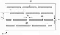
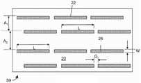
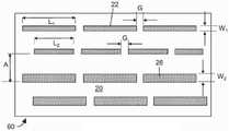
在一个实施例中,当从上方观看准直层时,细长腔室被设置为行和列,其中,细长腔室的较长尺寸沿着行延伸,并且其中,行与彼此之间的间隔是细长腔室宽度的至少三倍。通常,当从上方观看准直层时,细长腔室被设置为行和列,并且同一行内的相邻细长腔室之间的间隙小于30μm。在一些实施例中,在第一行中的相邻细长腔室之间的间隙相对于在第二行中的相邻细长腔室之间的间隙水平地偏移。在一些实施例中,通过改变细长腔室的长度、细长腔室的宽度、细长腔室的节距或细长腔室之间的间隙的宽度或位置来破坏细长腔室的对称性。In one embodiment, when the collimation layer is viewed from above, the elongated chambers are arranged in rows and columns, wherein the longer dimension of the elongated chambers extends along the rows, and wherein the rows and each other are The spacing is at least three times the width of the elongated chamber. Typically, when the collimation layer is viewed from above, the elongated chambers are arranged in rows and columns, and the gap between adjacent elongated chambers within the same row is less than 30 μm. In some embodiments, the gaps between adjacent elongated chambers in the first row are horizontally offset relative to the gaps between adjacent elongated chambers in the second row. In some embodiments, the symmetry of the elongated chambers is broken by changing the length of the elongated chambers, the width of the elongated chambers, the pitch of the elongated chambers, or the width or position of the gaps between the elongated chambers sex.
在另一方面,本发明包括一种显示器,该显示器具有光源、可切换的光准直膜、薄膜晶体管的有源矩阵、液晶层和彩色滤光片阵列。可切换的光准直膜包括第一透光电极层、厚度至少为20μm且包括多个细长腔室的准直层、以及第二透光电极层,其中第一透光层和第二透光层布置在准直层的两侧。细长腔室容纳包含颜料粒子的双稳态电泳流体,并且细长腔室用密封层密封,该密封层跨越细长腔室的开口。In another aspect, the invention includes a display having a light source, a switchable light-collimating film, an active matrix of thin film transistors, a liquid crystal layer, and a color filter array. The switchable light-collimating film includes a first light-transmitting electrode layer, a collimation layer having a thickness of at least 20 μm and including a plurality of elongated cavities, and a second light-transmitting electrode layer, wherein the first light-transmitting layer and the second light-transmitting layer are The optical layers are arranged on both sides of the collimation layer. The elongated chamber contains a bistable electrophoretic fluid containing pigment particles, and the elongated chamber is sealed with a sealing layer spanning the opening of the elongated chamber.
在一些实施例中,光准直膜或显示器附加地包括电压源和控制器,以在第一透光电极层和第二透光电极层之间提供电压冲激。在一些实施例中,显示器包括布置在光源和可切换的光准直膜之间的棱镜膜。在一些实施例中,显示器包括在棱镜膜和光源之间的扩散层。在一些实施例中,显示器包括触摸屏层。In some embodiments, the light-collimating film or display additionally includes a voltage source and a controller to provide voltage impulses between the first light-transmitting electrode layer and the second light-transmitting electrode layer. In some embodiments, the display includes a prismatic film disposed between the light source and the switchable light-collimating film. In some embodiments, the display includes a diffusing layer between the prismatic film and the light source. In some embodiments, the display includes a touch screen layer.
附图说明Description of drawings
图1A示出了可切换的光准直膜的第一状态,其中电泳粒子分布遍及准直层的腔室。电泳粒子在该状态中是稳定的,而无需施加电源;Figure 1A shows a first state of a switchable light-collimating film in which electrophoretic particles are distributed throughout the cavity of the collimating layer. Electrophoretic particles are stable in this state without applying power;
图1B示出了可切换的光准直膜的第二状态,其中,在施加电势的情况下,电泳粒子被驱动朝向第一透光电极;FIG. 1B shows a second state of the switchable light-collimating film in which electrophoretic particles are driven toward the first light-transmitting electrode under an applied electrical potential;
图1C示出了可切换的光准直膜的第三状态,其中电泳粒子在第一透光电极附近聚集。即使移除电势之后,粒子仍在该位置稳定;Figure 1C shows a third state of the switchable light-collimating film in which electrophoretic particles are concentrated near the first light-transmitting electrode. Even after removing the potential, the particle is still stable in that position;
图1D示出了返回到其中电泳粒子分布遍及准直层的腔室的状态;FIG. 1D shows the state returned to the chamber in which the electrophoretic particles are distributed throughout the collimation layer;
图1E示出了可切换的光准直膜的第四状态,其中,在施加具有图1B的相反极性的电势的情况下,电泳粒子被驱动朝向第二透光电极;FIG. 1E shows a fourth state of the switchable light-collimating film in which the electrophoretic particles are driven towards the second light-transmitting electrode under the application of a potential having the opposite polarity of FIG. 1B ;
图1F示出了可切换的光准直膜的第五状态,其中电泳粒子在第二透光电极附近聚集。即使移除电势之后,粒子仍在该位置稳定;Figure 1F shows a fifth state of the switchable light-collimating film in which electrophoretic particles are concentrated near the second light-transmitting electrode. Even after removing the potential, the particle is still stable in that position;
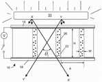
图2A示出了当电泳粒子分布遍及准直层的腔室时,从源发射的光线被限制在角度θ1;FIG. 2A shows that when electrophoretic particles are distributed throughout the chamber of the collimating layer, the light emitted from the source is confined to an angle θ1 ;
图2B示出了当电泳粒子被聚集紧靠最接近光源的透光电极时,从源发射的光线成角度θ2,其中θ2>>θ1;FIG. 2B shows that when the electrophoretic particles are gathered against the light-transmitting electrode closest to the light source, the light rays emitted from the source are at an angle θ2 , where θ2 >>θ1 ;
图2C示出了当电泳粒子被聚集紧靠最远离光源的透光电极时,从源发射的光线成角度θ3,其中θ3>>θ1。观察到由于在光准直膜的发射侧存在颜料粒子而使光损耗最小;Figure 2C shows that when the electrophoretic particles are focused against the light-transmitting electrode furthest from the light source, the light rays emitted from the source are atan angleΘ3 , whereΘ3 >> Θ1. Minimal loss of light was observed due to the presence of pigment particles on the emissive side of the light-collimating film;
图3示出了包括可切换的光准直膜的液晶显示器组件的有效层。层未按比例缩放;Figure 3 shows the active layers of a liquid crystal display assembly including a switchable light-collimating film. layers are not scaled;
图4示出了包括可切换的光准直膜和触摸屏的液晶显示器组件的有效层。层未按比例缩放;Figure 4 shows the active layers of a liquid crystal display assembly including a switchable light-collimating film and a touch screen. layers are not scaled;
图5示出了包括可切换的光准直膜和棱镜膜的液晶显示器组件的有效层。层未按比例缩放;Figure 5 shows the active layers of a liquid crystal display assembly including a switchable light-collimating film and a prismatic film. layers are not scaled;
图6示出了布置在下基板上的可切换的光准直膜的实施例。可切换的光准直膜附加地包括边缘密封件。分解视图详述了填充有双稳态电泳流体的细长腔室顶部上的密封层;Figure 6 shows an embodiment of a switchable light-collimating film disposed on a lower substrate. The switchable light-collimating film additionally includes an edge seal. An exploded view detailing the sealing layer on top of the elongated chamber filled with bistable electrophoretic fluid;
图7示出了可切换的光准直膜,其在一侧上具有光学透明的粘合剂和释放片。这样的膜可以例如用于在现有表面(例如玻璃窗)上提供准直特征;Figure 7 shows a switchable light-collimating film with an optically clear adhesive and release sheet on one side. Such films can be used, for example, to provide collimation features on existing surfaces such as glazing;
图8示出了可用于形成具有多个细长腔室的准直层并随后用双稳态电泳流体填充细长腔室并密封所填充的细长腔室的卷对卷工艺;8 illustrates a roll-to-roll process that can be used to form a collimation layer having a plurality of elongated chambers and subsequently fill the elongated chambers with a bistable electrophoretic fluid and seal the filled elongated chambers;
图9A和9B示出了简化的压印工艺;9A and 9B illustrate a simplified imprinting process;
图10详述了用于形成压印工具以创建本发明的准直层的方法;Figure 10 details a method for forming an imprint tool to create the alignment layer of the present invention;
图11详述了用于形成在压印工具中使用的垫片的方法;Figure 11 details a method for forming a shim for use in an imprint tool;
图12详述了用于形成在压印工具中使用的垫片的替代方法;Figure 12 details an alternative method for forming a shim for use in an imprint tool;
图13是可切换的光准直膜的实施例的顶视图,其中细长腔室被设置成行-列的形式;13 is a top view of an embodiment of a switchable light-collimating film in which elongated chambers are arranged in row-column form;
图14是可切换的光准直膜的实施例的顶视图,其中细长腔室被设置成行-列的形式;14 is a top view of an embodiment of a switchable light-collimating film in which elongated chambers are arranged in row-column format;
图15是可切换的光准直膜的实施例的顶视图,其中,同一行中的细长腔室之间的间隙的位置在连续行之间在一个方向上前进,从而破坏列的对称性;15 is a top view of an embodiment of a switchable light-collimating film in which the positions of the gaps between elongated chambers in the same row advance in one direction between successive rows, thereby breaking the symmetry of the columns ;
图16是可切换的光准直膜的实施例的顶视图,其中在同一行中的细长腔室的间隙的尺寸在连续行之间是不同的,从而破坏列的对称性;16 is a top view of an embodiment of a switchable light-collimating film in which the size of the gaps of elongated chambers in the same row is different between successive rows, thereby breaking the symmetry of the columns;
图17是可切换的光准直膜的实施例的顶视图,其中连续行之间的节距变化,从而破坏行的对称性;17 is a top view of an embodiment of a switchable light-collimating film in which the pitch between successive rows is varied, thereby breaking the symmetry of the rows;
图18是可切换的光准直膜的实施例的顶视图,其中腔室的长度和/或宽度在连续行之间变化,从而破坏行和列的对称性。18 is a top view of an embodiment of a switchable light-collimating film in which the length and/or width of the chambers vary between successive rows, thereby breaking row and column symmetry.
具体实施方式Detailed ways
如上所述,本发明提供了一种光准直膜,其包括双稳态电泳流体的细长腔室。这样的膜本身可以用于控制入射到透射基板的光的量和/或方向。这样的膜还可以被集成到诸如LCD显示器的装置中,以提供有用的特征,例如为观看LCD显示器的用户提供防窥区域。因为光准直膜是可切换的,所以它允许用户根据需要改变发射光的准直。另外,因为介质是双稳态的,所以准直状态将稳定一段时间,例如数分钟、例如数小时、例如数天、例如数月,而无需向光准直膜提供额外的能量。As described above, the present invention provides a light-collimating film comprising an elongated chamber of a bistable electrophoretic fluid. Such films themselves can be used to control the amount and/or direction of light incident on the transmissive substrate. Such films can also be integrated into devices such as LCD displays to provide useful features, such as providing a privacy-protected area for users viewing the LCD display. Because the light-collimating film is switchable, it allows the user to change the collimation of the emitted light as desired. Additionally, because the medium is bistable, the collimated state will be stable for a period of time, such as minutes, such as hours, such as days, such as months, without the need to provide additional energy to the light-collimating film.
本发明使得能够使用卷对卷工艺廉价地制造可切换的光准直膜。因此,生产大片可切换的光准直膜是可行的,该可切换的光准直膜可以在其他组装过程(诸如LCD显示器的制造)期间结合到装置中。这样的膜可以包括辅助的光学透明的粘合剂层和释放片,从而允许将光准直膜作为成品运输和配送。光准直膜也可以用于售后市场(after-market)的光控制,例如用于会议室窗户、建筑物的外窗以及遮阳天窗和天窗。The present invention enables the inexpensive manufacture of switchable light-collimating films using a roll-to-roll process. Therefore, it is feasible to produce large sheets of switchable light-collimating films that can be incorporated into devices during other assembly processes, such as the manufacture of LCD displays. Such films may include a secondary optically clear adhesive layer and release sheet, allowing the light-collimating film to be shipped and distributed as a finished product. Light collimating films can also be used for after-market light control, such as for conference room windows, exterior windows of buildings, and sunroofs and skylights.
电泳显示器通常包括电泳材料层和布置在电泳材料的相对侧上的至少两个其他层,这两个层之一是电极层。在大多数这样的显示器中,两个层都是电极层,并且电极层中的一个或两个被图案化以限定显示器的像素。例如,一个电极层可以被图案化为细长的行电极,而另一个可以被图案化为与行电极成直角延伸的细长的列电极,像素由行电极和列电极的交叉点限定。可替代地,并且更通常地,一个电极层具有单个连续电极的形式,而另一电极层被图案化成像素电极的矩阵,每个像素电极限定显示器的一个像素。在一些实施例中,使用两个透光电极层,从而允许光穿过电泳显示器。Electrophoretic displays typically comprise a layer of electrophoretic material and at least two other layers, one of which is an electrode layer, arranged on opposite sides of the electrophoretic material. In most such displays, both layers are electrode layers, and one or both of the electrode layers are patterned to define the pixels of the display. For example, one electrode layer may be patterned as elongated row electrodes, while the other may be patterned as elongated column electrodes extending at right angles to the row electrodes, with pixels defined by intersections of the row and column electrodes. Alternatively, and more typically, one electrode layer has the form of a single continuous electrode, while the other electrode layer is patterned into a matrix of pixel electrodes, each pixel electrode defining a pixel of the display. In some embodiments, two light transmissive electrode layers are used, allowing light to pass through the electrophoretic display.
术语“双稳态的”和“双稳定性”在此使用的是其在本领域中的常规含义,指的是包括具有第一和第二显示状态的显示元件的显示器,所述第一和第二显示状态的至少一个光学特性不同,从而在利用有限持续时间的寻址脉冲驱动任何给定元件以呈现其第一或第二显示状态之后,在该寻址脉冲终止后,该状态将持续的时间是用于改变该显示元件的状态所需的寻址脉冲的最小持续时间的至少几倍(例如至少4倍)。在美国专利No.7,170,670中示出,支持灰度的一些基于粒子的电泳显示器不仅可以稳定于其极端的黑色和白色状态,还可以稳定于其中间的灰色状态,以及一些其它类型的电光显示器也是如此。这种类型的显示器被恰当地称为是“多稳态的”而非双稳态的,但是为了方便,在此可使用术语“双稳态的”以同时涵盖双稳态的和多稳态的显示器。The terms "bistable" and "bistable" are used herein in their conventional meanings in the art to refer to a display that includes display elements having first and second display states, the first and second The second display state differs in at least one optical property such that after any given element is driven with an addressing pulse of limited duration to assume its first or second display state, that state will persist after the addressing pulse has terminated is at least several times (eg, at least 4 times) the minimum duration of an addressing pulse required to change the state of the display element. It is shown in US Patent No. 7,170,670 that some particle-based electrophoretic displays that support grayscale are stable not only in their extreme black and white states, but also in their intermediate gray state, as are some other types of electro-optic displays in this way. This type of display is properly referred to as "multi-stable" rather than bistable, but for convenience the term "bistable" may be used herein to cover both bistable and multi-stable display.
可切换的光准直膜(10)的一般功能在图1A-1F中示出。膜(10)包括第一透光电极层(12)和第二透光电极层(14)。通常,每个电极层分别与第一基板(16)和第二基板(18)相关联。第一基板(16)和第二基板(18)可以是透光聚合物(例如,膜或树脂)或玻璃。在用卷对卷工艺生产膜(10)的情况下,第一基板(16)和第二基板(18)是柔性的。透光电极和基板也可以集成到单个层中,例如PET-ITO膜、PEDOT或掺杂有导电材料(例如石墨烯、纳米管、金属薄片、导电金属氧化物粒子或金属纤维)和/或掺杂有导电单体或聚合物和/或掺杂有离子材料(例如盐)的另一种透光聚合物。The general function of the switchable light-collimating film (10) is shown in Figures 1A-1F. The film (10) includes a first light transmissive electrode layer (12) and a second light transmissive electrode layer (14). Typically, each electrode layer is associated with a first substrate (16) and a second substrate (18), respectively. The first substrate (16) and the second substrate (18) may be a light transmissive polymer (eg, film or resin) or glass. In the case of producing the film (10) with a roll-to-roll process, the first substrate (16) and the second substrate (18) are flexible. Light-transmitting electrodes and substrates can also be integrated into a single layer, such as PET-ITO films, PEDOT or doped with conductive materials (such as graphene, nanotubes, metal flakes, conductive metal oxide particles or metal fibers) and/or doped with Another light transmissive polymer doped with conductive monomers or polymers and/or doped with ionic materials such as salts.
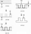
光准直层(21)包括透光聚合物(20),其已经被处理以产生多个细长腔室(22)以容纳包括电泳粒子(26)的双稳态电泳流体(24)。在实施例中,双稳态电泳流体(24)包括烃类溶剂,并且电泳粒子(26)包括炭黑(如下文所述,可选地官能化)。光准直层至少为20μm厚(即,第一透光电极层(12)和第二透光电极层(14)之间的距离)。光准直层的厚度可以大于20μm,例如大于30μm、例如大于50μm、例如大于70μm、例如大于100μm、例如大于150μm、例如大于200μm。细长腔室的制造,例如通过压印热塑性塑料,将在下面更详细地描述。在填充细长腔室(22)的过程之后或期间,细长腔室(22)用密封层(28)密封,密封层(28)可以是例如与双稳态电泳流体(24)不相容的亲水性聚合物。The light collimating layer (21) comprises a light transmissive polymer (20) which has been processed to create a plurality of elongated chambers (22) to accommodate a bistable electrophoretic fluid (24) comprising electrophoretic particles (26). In an embodiment, the bistable electrophoretic fluid (24) comprises a hydrocarbon solvent and the electrophoretic particles (26) comprise carbon black (optionally functionalized as described below). The light-collimating layer is at least 20 μm thick (ie, the distance between the first light-transmitting electrode layer (12) and the second light-transmitting electrode layer (14)). The thickness of the light collimating layer may be greater than 20 μm, such as greater than 30 μm, such as greater than 50 μm, such as greater than 70 μm, such as greater than 100 μm, such as greater than 150 μm, such as greater than 200 μm. The manufacture of elongated chambers, for example by stamping thermoplastics, will be described in more detail below. After or during the process of filling the elongated chamber (22), the elongated chamber (22) is sealed with a sealing layer (28), which may be, for example, incompatible with the bistable electrophoretic fluid (24). of hydrophilic polymers.
为了改变膜(10)的准直特性,第一透光电极层(12)和第二透光电极层(14)可以耦合到电势源(30)。该源可以例如是电池、电源、光伏或某些其他电势源。该源可以提供简单的直流(D.C.)电势,或者可以被配置为提供随时间变化的电压,例如,如下所述的“波形”。第一透光电极层(12)和第二透光电极层(14)可以经由电极、导线或迹线(31)耦合到源(30)。在一些实施例中,迹线(31)可以被开关(32)中断,该开关可以例如是晶体管开关。第一透光电极层(12)和第二透光电极层(14)之间的电势通常为至少1伏特,例如至少2伏特、例如至少5伏特、例如至少10伏特、例如至少15伏特、例如至少18伏特、例如至少25伏特、例如至少30伏特、例如至少30伏特、例如至少50伏特。To alter the collimation properties of the film (10), the first light transmissive electrode layer (12) and the second light transmissive electrode layer (14) may be coupled to a potential source (30). The source may be, for example, a battery, power supply, photovoltaic or some other potential source. The source may provide a simple direct current (D.C.) potential, or may be configured to provide a time-varying voltage, eg, a "waveform" as described below. The first light transmissive electrode layer (12) and the second light transmissive electrode layer (14) may be coupled to the source (30) via electrodes, wires or traces (31). In some embodiments, the trace (31) may be interrupted by a switch (32), which may be, for example, a transistor switch. The potential between the first light transmissive electrode layer (12) and the second light transmissive electrode layer (14) is typically at least 1 volt, such as at least 2 volts, such as at least 5 volts, such as at least 10 volts, such as at least 15 volts, such as At least 18 volts, such as at least 25 volts, such as at least 30 volts, such as at least 30 volts, such as at least 50 volts.
因为双稳态电泳流体(24)是双稳态的,所以电泳粒子(26)将保持其分布而无需施加电场。该特征在本文中列出的伊英克公司的专利中很好地描述,但是主要是由于在双稳态电泳流体(24)中具有分布聚合物的特定混合物(例如聚异丁烯或聚甲基丙烯酸月桂酯)所致,使得电泳粒子(26)通过空缺絮凝(depletion flocculation)而稳定。因此,在图1A所示的第一状态中,电泳粒子(26)稳定于分散状态,尽管在第一透光电极层(12)和第二透光电极层(14)之间没有施加电势。通过施加适当的电势,例如,如图1B所示,电泳粒子(26)朝着适当偏压的电极层移动,从而沿着细长腔室(22)的高度创建透光梯度。一旦电泳粒子(26)被驱动到期望的电极层,则源(30)可以与电极层解耦,从而关闭电势。然而,由于双稳态电泳流体(24)的双稳定性,电泳粒子(26)将长时间保持在第二状态,例如数分钟、例如数小时、例如数天,如图1C所示。Because the bistable electrophoretic fluid (24) is bistable, the electrophoretic particles (26) will maintain their distribution without the need to apply an electric field. This feature is well described in the Iink Corporation patents listed here, but is primarily due to having specific mixtures of distributed polymers (such as polyisobutylene or polylauryl methacrylate) in the bistable electrophoretic fluid (24) Ester), the electrophoretic particles (26) are stabilized by depletion flocculation. Therefore, in the first state shown in FIG. 1A , the electrophoretic particles ( 26 ) are stable in a dispersed state, although no potential is applied between the first light-transmitting electrode layer ( 12 ) and the second light-transmitting electrode layer ( 14 ). By applying an appropriate electrical potential, eg, as shown in Figure IB, the electrophoretic particles (26) move towards a suitably biased electrode layer, thereby creating a light transmission gradient along the height of the elongated chamber (22). Once the electrophoretic particles (26) are driven to the desired electrode layer, the source (30) can be decoupled from the electrode layer, thereby turning off the potential. However, due to the bistability of the bistable electrophoretic fluid (24), the electrophoretic particles (26) will remain in the second state for a long time, such as minutes, such as hours, such as days, as shown in Figure 1C.
可以通过用反极性电压(未示出)驱动聚集的电泳粒子(26)远离电极来使光准直膜(10)的状态反转,以实现图1D。当返回初始状态(相当于1A)时,只有(大致)准直的光将能够通过光准直膜,如下文更详细地描述。图1D的状态也是稳定的。通过施加图1B的反极性电压,可以将电泳粒子(26)驱动通过该分布状态并朝向第二透光电极(14),如图1E所示。结果,如下所讨论的,电泳粒子(26)将邻近第二透光电极(14)聚集,这也导致了宽视角。图1F所示的广角透射状态也是双稳态的,也就是说,不需要电源即可维持该状态。因为图1C和图1F的状态都导致广角透射,所以可以在图1A、1C、1D和1F所示的状态之间切换,同时保持驱动电子设备的总体DC平衡。DC平衡驱动电子设备可减少电荷累积并延长系统组件的寿命。The state of the light-collimating film (10) can be reversed by driving the aggregated electrophoretic particles (26) away from the electrodes with a voltage of reverse polarity (not shown) to achieve Figure ID. When returning to the initial state (equivalent to 1A), only (roughly) collimated light will be able to pass through the light-collimating film, as described in more detail below. The state of FIG. 1D is also stable. By applying the reverse polarity voltage of Figure IB, the electrophoretic particles (26) can be driven through this distribution and towards the second light-transmitting electrode (14), as shown in Figure 1E. As a result, as discussed below, the electrophoretic particles (26) will aggregate adjacent to the second light transmissive electrode (14), which also results in a wide viewing angle. The wide-angle transmissive state shown in Figure IF is also bistable, that is, no power supply is required to maintain this state. Because the states of FIGS. 1C and 1F both result in wide-angle transmission, it is possible to switch between the states shown in FIGS. 1A , 1C, 1D and 1F while maintaining the overall DC balance of the drive electronics. DC balanced drive electronics reduce charge build-up and extend the life of system components.
电泳介质的内相包括悬浮流体中的带电颜料粒子。在本发明的可变透射介质中使用的流体通常将具有低介电常数(优选地小于10,并且期望小于3)。特别优选的溶剂包括脂族烃,例如庚烷、辛烷和石油馏出物,例如


带电颜料粒子可以具有多种颜色和组分。另外,带电颜料粒子可以用表面聚合物官能化以改善状态稳定性。这样的颜料在美国专利公开No.2016/0085132中描述,其全部内容通过引用包含于此。例如,如果带电粒子为白色,则它们可以由诸如TiO2、ZrO2、ZnO、Al2O3、Sb2O3、BaSO4、PbSO4等的无机颜料形成。它们也可以是具有高折射率(>1.5)且具有一定尺寸(>100nm)以显示白色的聚合物粒子,或者是被设计制造以具有期望的折射率的复合粒子。黑色带电粒子可以由CI颜料黑26或28等(例如铁锰黑或铜铬黑)或炭黑形成。其他颜色(非白色和非黑色)可以由有机颜料形成,例如CI颜料PR254、PR122、PR149、PG36、PG58、PG7、PB28、PB15:3、PY83、PY138、PY150、PY155或PY20。其他示例包括科莱恩(Clariant)的Hostaperm Red D3G 70-EDS、Hostaperm Pink E-EDS、PV fast red D3G、Hostaperm RedD3G 70、Hostaperm Blue B2G-EDS、Hostaperm Yellow H4G-EDS、Novoperm Yellow HR-70-EDS、Hostaperm Green GNX、巴斯夫(BASF)的Irgazine Red L 3630、Cinquasia Red L4100HD和Irgazin Red L 3660HD;太阳化学(Sun Chemical)的酞菁蓝、酞菁绿、苯胺黄或联苯胺黄。彩色粒子也可以由无机颜料形成,例如CI颜料蓝28、CI颜料绿50、CI颜料黄227等。带电粒子的表面可以通过已知技术基于粒子所需的电荷极性和电荷水平进行修改,如在美国专利No.6,822,782、7,002,728、9,366,935和9,372,380以及美国公开No.2014-0011913中所描述的,上述专利的全部内容通过引用包含于此。Charged pigment particles can have a variety of colors and compositions. Additionally, charged pigment particles can be functionalized with surface polymers to improve state stability. Such pigments are described in US Patent Publication No. 2016/0085132, the entire contents of which are incorporated herein by reference. For example, if the charged particles are white, they may be formed from inorganicpigments such asTiO2 ,ZrO2 , ZnO,Al2O3 ,Sb2O3 ,BaSO4 ,PbSO4 , and the like. They can also be polymer particles with a high refractive index (>1.5) and a certain size (>100 nm) to appear white, or composite particles designed to have the desired refractive index. The black charged particles may be formed from
粒子可以表现出天然电荷,或者它们可以使用电荷控制剂使其明确地带电,或者当悬浮在溶剂或溶剂混合物中时可以获取电荷。合适的电荷控制剂是本领域公知的;它们本质上可以是聚合的或非聚合的,或者可以是离子的或非离子的。电荷控制剂的示例可以包括但不限于Solsperse 17000(活性聚合物分散剂)、Solsperse 9000(活性聚合物分散剂)、OLOA 11000(琥珀酰亚胺无灰分散剂)、Unithox 750(乙氧基化物)、Span 85(脱水山梨糖醇三油酸酯)、Petronate L(磺酸钠)、Alcolec LV30(大豆卵磷脂)、Petrostep B100(石油磺酸盐)或B70(磺酸钡)、Aerosol OT、聚异丁烯衍生物或聚(乙烯共-丁烯)衍生物等。除了悬浮流体和带电颜料粒子外,内相可以包括稳定剂、表面活性剂和电荷控制剂。当带电颜料粒子分散在溶剂中时,稳定材料可以吸附在带电颜料粒子上。这种稳定材料保持粒子彼此分离,使得当粒子处于其分散状态时,可变透射介质基本上是不透射的。如本领域中已知的,可以通过使用表面活性剂来辅助将带电粒子(如上所述,通常为炭黑)分散在低介电常数的溶剂中。这样的表面活性剂通常包含极性“头基”和与溶剂相容或可溶于溶剂的非极性“尾基”。在本发明中,优选地,非极性尾基为饱和或不饱和烃部分,或可溶于烃类溶剂(例如聚(二烷基硅氧烷))的另一基团。极性基团可以是任何极性有机官能团,包括离子材料,例如铵盐、磺酸盐或膦酸盐,或酸性或碱性基团。特别优选地,头基是羧酸或羧酸盐基团。适用于本发明的稳定剂包括聚异丁烯和聚苯乙烯。在一些实施例中,添加分散剂,例如聚异丁烯丁二酰亚胺和/或脱水山梨糖醇三油酸酯和/或2-己基癸酸。Particles can exhibit a natural charge, or they can be explicitly charged using charge control agents, or can acquire a charge when suspended in a solvent or solvent mixture. Suitable charge control agents are well known in the art; they may be polymeric or non-polymeric in nature, or ionic or non-ionic. Examples of charge control agents may include, but are not limited to, Solsperse 17000 (active polymeric dispersant), Solsperse 9000 (active polymeric dispersant), OLOA 11000 (succinimide ashless dispersant), Unithox 750 (ethoxylate) , Span 85 (sorbitan trioleate), Petronate L (sodium sulfonate), Alcolec LV30 (soy lecithin), Petrostep B100 (petroleum sulfonate) or B70 (barium sulfonate), Aerosol OT, Polyester isobutylene derivatives or poly(ethylene co-butene) derivatives, etc. In addition to the suspending fluid and charged pigment particles, the internal phase may include stabilizers, surfactants, and charge control agents. When the charged pigment particles are dispersed in a solvent, the stabilizing material can be adsorbed on the charged pigment particles. This stabilizing material keeps the particles separate from each other such that the variable transmission medium is substantially opaque when the particles are in their dispersed state. Dispersion of charged particles (usually carbon black, as described above) in low dielectric constant solvents can be aided by the use of surfactants, as is known in the art. Such surfactants typically contain a polar "head group" and a solvent-compatible or solvent-soluble non-polar "tail group". In the present invention, preferably, the non-polar tail group is a saturated or unsaturated hydrocarbon moiety, or another group that is soluble in hydrocarbon solvents such as poly(dialkylsiloxanes). The polar group can be any polar organic functional group, including ionic materials such as ammonium, sulfonate, or phosphonate, or acidic or basic groups. Particularly preferably, the head group is a carboxylic acid or carboxylate group. Stabilizers suitable for use in the present invention include polyisobutylene and polystyrene. In some embodiments, dispersants such as polyisobutylene succinimide and/or sorbitan trioleate and/or 2-hexyldecanoic acid are added.
本发明的电泳介质通常将包含电荷控制剂(CCA),并且可以包含电荷引导剂。这些电泳介质组分通常包含低分子量表面活性剂、聚合剂或一种或多种组分的混合物,并用于稳定或以其他方式修改电泳粒子上电荷的符号和/或大小。CCA通常是包含离子或其他极性基团(以下称为头基)的分子。正或负离子头基中的至少一个优选地附接至非极性链(通常为烃链),该非极性链在下文中称为尾基。据认为,CCA在内相中形成反胶团,并且是少数带电的反胶团,其导致通常用作电泳流体的非极性流体中的电导率。The electrophoretic medium of the present invention will typically contain a charge control agent (CCA), and may contain a charge director. These electrophoretic medium components typically contain low molecular weight surfactants, polymeric agents, or a mixture of one or more components, and are used to stabilize or otherwise modify the sign and/or size of the charge on the electrophoretic particles. CCAs are typically molecules containing ionic or other polar groups (hereinafter referred to as head groups). At least one of the positive or negative ionic head groups is preferably attached to a non-polar chain (usually a hydrocarbon chain), hereinafter referred to as the tail group. It is believed that CCA forms reverse micelles in the internal phase, and is a minority of charged reverse micelles, which contribute to the electrical conductivity in non-polar fluids commonly used as electrophoretic fluids.
反胶团包含被CCA分子的非极性尾基包围的高极性核(通常含有水),其大小可以在1nm至数十纳米变化(并且可以具有球形、圆柱形或其他几何形状)。反胶团已经被广泛研究,特别是在诸如油/水/表面活性剂混合物的三元混合物中。一个示例是异辛烷/水/AOT混合物,例如在Fayer等,J.Chem.Phys.,131,14704(2009)中所描述的。在电泳介质中,通常可以区分出三个相:具有表面的固体粒子、以极小的微滴(反胶团)形式分布的高极性相以及包含流体的连续相。在施加电场时,带电粒子和带电反胶团都可以移动通过流体,因此,存在两条平行的路径电传导通过流体(其本身通常具有非常小的电导率)。Inverse micelles contain a highly polar core (usually containing water) surrounded by non-polar tails of CCA molecules, which can vary in size from 1 nm to tens of nanometers (and can have spherical, cylindrical, or other geometric shapes). Inverse micelles have been extensively studied, especially in ternary mixtures such as oil/water/surfactant mixtures. An example is isooctane/water/AOT mixtures such as described in Fayer et al., J. Chem. Phys., 131, 14704 (2009). In an electrophoretic medium, three phases can generally be distinguished: solid particles with a surface, a highly polar phase distributed in the form of extremely small droplets (inverse micelles), and a continuous phase containing fluid. When an electric field is applied, both charged particles and charged reverse micelles can move through the fluid, so there are two parallel paths of electrical conduction through the fluid (which themselves typically have very little conductivity).
CCA的极性核被认为通过吸附到表面上而影响表面上的电荷。在电泳显示器中,这种吸附可以在电泳粒子的表面或微囊体的内壁(或其他固体相,例如微单元的壁)上,以形成类似于反胶团的结构,这些结构在下文中称为半胶团。当离子对中的一个离子比另一个离子更牢固地附着至表面时(例如,通过共价键结合),半胶团和未结合的反胶团之间的离子交换可导致电荷分离,其中更牢固地结合的离子保持与粒子相关联,而较不牢固地结合的离子将结合到游离的反胶团的核中。The polar nuclei of CCA are thought to influence the charge on the surface by adsorbing to the surface. In electrophoretic displays, this adsorption can be on the surface of electrophoretic particles or on the inner walls of microcapsules (or other solid phases, such as the walls of microcells) to form structures similar to inverse micelles, which are hereinafter referred to as Semi-mosaic. When one ion in an ion pair is more strongly attached to a surface than the other (eg, by covalent bonding), ion exchange between the hemimicelles and the unbound reverse micelles can lead to charge separation, with more The strongly bound ions remain associated with the particles, while the less strongly bound ions will be bound into the core of the free reverse micelles.
形成CCA的头基的离子材料还可以在电泳粒子(或其他)表面处诱导离子对形成。因此,CCA可以执行两个基本功能:在表面处生成电荷和从表面分离电荷。电荷生成可以是由CCA分子中存在的或以其他方式结合到反胶团核或流体中的某些部分与粒子表面之间的酸-碱或离子交换反应所造成的。因此,有用的CCA材料是那些能够参与这样的反应或本领域已知的任何其他充电反应(charging reaction)的材料。当用光照射粒子时,CCA分子可以另外充当由电泳粒子产生的光激子的受体。The ionic material that forms the head group of the CCA can also induce ion pair formation at the electrophoretic particle (or other) surface. Therefore, CCA can perform two basic functions: generating charge at the surface and separating charge from the surface. Charge generation may result from acid-base or ion exchange reactions between certain moieties present in the CCA molecule or otherwise incorporated into the reverse micelle core or fluid and the particle surface. Accordingly, useful CCA materials are those capable of participating in such reactions or any other charging reaction known in the art. When the particles are irradiated with light, CCA molecules can additionally act as acceptors for photoexcitons generated by the electrophoretic particles.
在本发明的介质中有用的电荷控制剂的非限制性种类包括有机硫酸盐或磺酸盐、金属皂、嵌段或梳型共聚物、有机酰胺、有机两性离子、以及有机磷酸盐和膦酸酯。有用的有机硫酸盐和磺酸盐包括但不限于,双(2-乙基己基)磺基琥珀酸钠、十二烷基苯磺酸钙、石油磺酸钙、中性或碱性二壬基萘磺酸钡、中性或碱性二壬基萘磺酸钙、十二烷基苯磺酸钠盐和十二烷基硫酸铵。有用的金属皂包括但不限于,碱性或中性石油磺酸钡(bariumpetronate)、石油磺酸钙、羧酸(例如环烷酸、辛酸、油酸、棕榈酸、硬脂酸和肉豆蔻酸等)的钴、钙、铜、锰、镁、镍、锌、铝和铁盐。有用的嵌段或梳型共聚物包括但不限于,(A)由对甲苯磺酸甲酯季铵化的2-(N,N-二甲氨基)甲基丙烯酸乙酯的聚合物和(B)聚(2-乙基己基甲基丙烯酸盐)的AB二嵌段共聚物、以及侧接在聚(甲基丙烯酸甲酯-甲基丙烯酸)的油溶性锚固基团上的具有聚(12-羟基硬脂酸)的油溶性尾的分子量约为1800的梳型接枝共聚物。有用的有机酰胺/胺包括但不限于,聚异丁烯琥珀酰亚胺,例如OLOA 371或1200(可从德克萨斯州休斯顿(Houston,Tex.)的雪佛龙奥伦奈特公司(Chevron Oronite Company LLC)获得)或Solsperse 17000(可从俄亥俄州威克里夫(Wickliffe,OH)的路博润(Lubrizol)获得:Solsperse是注册商标)和N-乙烯吡咯烷酮聚合物。有用的有机两性离子包括但不限于卵磷脂。有用的有机磷酸盐和膦酸酯包括但不限于具有饱和和不饱和酸取代基的磷酸单甘油酯和二甘油酯的钠盐。对于CCA有用的尾基包括烯烃的聚合物,例如分子量在200-10000范围内的聚(异丁烯)。头基可以是磺酸、磷酸或羧酸或酰胺,或可替代地,氨基,例如伯、仲、叔或季铵基。Non-limiting classes of charge control agents useful in the media of the present invention include organic sulfates or sulfonates, metal soaps, block or comb copolymers, organic amides, organic zwitterions, and organic phosphates and phosphonic acids ester. Useful organic sulfates and sulfonates include, but are not limited to, sodium bis(2-ethylhexyl)sulfosuccinate, calcium dodecylbenzenesulfonate, calcium petroleum sulfonate, neutral or basic dinonyl Barium naphthalenesulfonate, neutral or basic calcium dinonylnaphthalenesulfonate, sodium dodecylbenzenesulfonate and ammonium dodecyl sulfate. Useful metal soaps include, but are not limited to, basic or neutral barium petronate, calcium petroleum sulfonate, carboxylic acids such as naphthenic, caprylic, oleic, palmitic, stearic and myristic acids etc.) cobalt, calcium, copper, manganese, magnesium, nickel, zinc, aluminum and iron salts. Useful block or comb copolymers include, but are not limited to, (A) polymers of ethyl 2-(N,N-dimethylamino)methacrylate quaternized with methyl p-toluenesulfonate and (B) ) AB diblock copolymer of poly(2-ethylhexyl methacrylate), and poly(12- hydroxystearic acid), a comb graft copolymer with a molecular weight of about 1800 in the oil-soluble tail. Useful organic amides/amines include, but are not limited to, polyisobutylene succinimides such as OLOA 371 or 1200 (available from Chevron Oronite, Houston, Tex.). Company LLC) or Solsperse 17000 (available from Lubrizol, Wickliffe, OH: Solsperse is a registered trademark) and N-vinylpyrrolidone polymer. Useful organic zwitterions include, but are not limited to, lecithin. Useful organophosphates and phosphonates include, but are not limited to, the sodium salts of mono- and diglyceride phosphates having saturated and unsaturated acid substituents. Useful tails for CCA include polymers of olefins, such as poly(isobutylene) having a molecular weight in the range of 200-10,000. The head group may be a sulfonic acid, phosphoric acid or carboxylic acid or amide, or alternatively, an amino group such as a primary, secondary, tertiary or quaternary ammonium group.
在本发明的介质中使用的电荷辅助剂可以使电泳粒子表面上的电荷偏置,如下文更详细地描述。这样的电荷辅助剂可以是布朗斯台德或路易斯酸或碱。The charge aids used in the media of the present invention can bias the charge on the surface of the electrophoretic particles, as described in more detail below. Such charge aids may be Bronsted or Lewis acids or bases.
可以添加粒子分散体稳定剂以防止粒子絮凝或附着到囊体或其他壁或表面。对于在电泳显示器中用作流体的典型的高电阻率液体,可以使用无水表面活性剂。这些包括但不限于,乙二醇醚、炔属乙二醇、烷醇酰胺、山梨糖醇衍生物、烷基胺、季胺、咪唑啉、二烷基氧化物和磺基琥珀酸酯。Particle dispersion stabilizers can be added to prevent particles from flocculating or adhering to capsules or other walls or surfaces. For typical high resistivity liquids used as fluids in electrophoretic displays, anhydrous surfactants can be used. These include, but are not limited to, glycol ethers, acetylenic glycols, alkanolamides, sorbitol derivatives, alkylamines, quaternary amines, imidazolines, dialkyl oxides, and sulfosuccinates.
如美国专利No.7,170,670中所述,可以通过在流体中包含数均分子量超过约20000的聚合物来改善电泳介质的双稳定性,该聚合物基本上不吸附在电泳粒子上;为此目的,聚(异丁烯)是优选的聚合物。As described in US Pat. No. 7,170,670, the bistability of electrophoretic media can be improved by including in the fluid a polymer having a number average molecular weight in excess of about 20,000 that is substantially not adsorbed on electrophoretic particles; for this purpose, Poly(isobutylene) is the preferred polymer.
此外,例如,如美国专利No.6,693,620中所述,在其表面上具有固定电荷的粒子在周围流体中建立相反电荷的双电层。CCA的离子头基可以与电泳粒子表面上的带电基团进行离子配对,形成一层固定的或部分固定的带电粒种。在该层的外部,存在一个扩散层,该扩散层包括在流体中包含CCA分子的带电的(反)胶团。在常规的DC电泳中,施加的电场在固定的表面电荷上施加力,而在可移动的反电荷上施加相反的力,使得在扩散层内发生滑移,并且粒子相对于流体移动。在滑移面处的电势称为ζ(zeta)电势。Furthermore, for example, as described in US Pat. No. 6,693,620, particles with fixed charges on their surfaces create an oppositely charged electric double layer in the surrounding fluid. The ionic head groups of CCA can ion-pair with charged groups on the surface of electrophoretic particles to form a layer of immobilized or partially immobilized charged species. Outside of this layer, there is a diffusion layer comprising charged (inverse) micelles containing CCA molecules in the fluid. In conventional DC electrophoresis, an applied electric field exerts a force on a fixed surface charge and an opposite force on a movable counter-charge, so that slip occurs within the diffusion layer and the particles move relative to the fluid. The potential at the slip plane is called the zeta (zeta) potential.
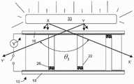
如图2A、2B和2C所示,所得到的光准直膜(10)可以用于变窄(准直)光(33)。在如图2A所示的第一变窄状态下,电泳粒子(26)分布遍及整个细长腔室(22),导致由细长腔室(22)之间的节距(A)、每个细长腔室(22)的宽度(W)、光准直膜(10)的高度(H)以及从光源(33)到出射基板(在图2A的示例中为基板(18))的距离限定的透射角θ1。从图2A中可以看出,角度θ1由光线X-X’和Y-Y’大致限定,光线X-X’和Y-Y’限定了光可以离开源(33)并通过电泳粒子(26)遍及分布的细长腔室(22)的顶部和底部的与法线的最大角度。As shown in Figures 2A, 2B and 2C, the resulting light collimating film (10) can be used to narrow (collimate) light (33). In the first narrowed state as shown in Figure 2A, the electrophoretic particles (26) are distributed throughout the elongated chambers (22), resulting in a spacing (A) between the elongated chambers (22), each The width (W) of the elongated chamber (22), the height (H) of the light-collimating film (10) and the distance from the light source (33) to the exit substrate (substrate (18) in the example of Figure 2A) define The transmission angle θ1 . As can be seen in Figure 2A, angleθ1 is roughly defined by rays XX' and YY', which define how light can exit the source (33) and pass through the electrophoretic particles (26). ) is the maximum angle to the normal at the top and bottom of the elongated chamber (22) distributed throughout.
在等效于上述图1C的第一广角状态中,电泳粒子(26)被驱动至更近的基板(16),并且如图2B所示,由光线X-X’和Y-Y’建立新的透射角θ2。如图2B所示,新的透射角θ2将比θ1宽得多,也就是说,θ2>>θ1。再次,透射角θ2的有效变窄将是细长腔室(22)之间的节距(A)、每个细长腔室(22)的宽度(W)和光准直膜(10)的高度(H)的函数。In the first wide-angle state equivalent to Figure 1C above, the electrophoretic particles (26) are driven to the closer substrate (16) and, as shown in Figure 2B, new light rays XX' and YY' establish a new The transmission angle θ2 . As shown in Figure 2B, the new transmission angle θ2 will be much wider than θ1 , that is, θ2 >> θ1 . Again, the effective narrowing of the transmission angle θ2 will be the pitch (A ) between the elongated chambers (22), the width (W) of each elongated chamber (22) and the width of the light-collimating film (10) A function of height (H).
在等效于上述图1F的第二广角状态中,电泳粒子(26)被驱动至远离光源(33)的基板(16),并且如图2C所示,由光线X-X’和Y-Y’建立新的透射角θ3。如图2C所示,新的透射角θ3将比θ1宽得多,也就是说,θ3>>θ1。如图2B,透射角θ3的有效变窄将是细长腔室(22)之间的节距(A)、每个细长腔室(22)的宽度(W)和光准直膜(10)的高度(H)的函数。此外,虽然似乎邻近第二基板(18)累积的电泳粒子(26)可能会投射出阴影,但这并未被观察到。推测是存在足够的散射光通过光准直膜(10)以消除这种效应。In the second wide-angle state equivalent to Fig. 1F above, the electrophoretic particles (26) are driven away from the substrate (16) of the light source (33) and, as shown in Fig. 2C, are driven by the rays XX' and Y-Y 'Establish a new transmission angle θ3 . As shown in Figure 2C, the new transmission angle θ3 will be much wider than θ1 , that is, θ3 >> θ1 . 2B, the effective narrowingof the transmission angle θ3 would be the pitch (A) between the elongated chambers (22), the width (W) of each elongated chamber (22), and the light-collimating film (10). ) as a function of height (H). Furthermore, although it appears that electrophoretic particles (26) accumulated adjacent to the second substrate (18) may cast shadows, this has not been observed. It is presumed that there is enough scattered light to pass through the light collimating film (10) to eliminate this effect.
预期在大多数配置中,在从宽透射角(图2B和2C)转变到窄透射角(图2A)期间,本发明的光准直膜(10)将提供至少减小两倍的有效观看面积(由作为与法线夹角的函数的小于50%的相对透射限定)。在一些实施例中,观看面积的减小将大于两倍,例如三倍、例如四倍。由于这种功能,光准直膜(10)在简单地应用于玻璃板(例如内部办公室窗户)时可能是有用的,由此可以极大地减小玻璃的透射角,从而增加了办公室使用者的防窥性,同时仍然允许良好的光线量透射通过窗户。It is expected that in most configurations, the light-collimating film (10) of the present invention will provide at least a two-fold reduction in effective viewing area during the transition from wide transmission angles (FIGS. 2B and 2C) to narrow transmission angles (FIG. 2A). (defined by less than 50% relative transmission as a function of angle from normal). In some embodiments, the reduction in viewing area will be greater than two times, such as three times, such as four times. Because of this function, the light-collimating film (10) may be useful when simply applied to glass panels (eg, interior office windows), whereby the transmission angle of the glass can be greatly reduced, thereby increasing the office user's Privacy while still allowing a good amount of light to transmit through the windows.
如图3所示,可以将光准直膜(10)结合到液晶显示器(LCD)堆叠(stack)中。图3是示例性的,因为LCD堆叠具有许多不同的配置。如图3所示,通常是一个或多个发光二极管(LED)的光(33)由导光板(34)和扩散板(35)的组合引导通过包括有源层的显示器堆叠。离开扩散板(35)的光沿观察者(图3顶部的眼睛)的方向传播,然后遇到上述类型的光准直膜(10)。在图3所示的状态下,光准直膜(10)将仅当光在较窄的透射角(见图2)内传播时才允许光通过有源层。穿过光准直膜(10)的光接下来将继续通过第一偏振膜(36)、包括多个像素电极(42)的有源矩阵薄膜晶体管(AM-TFT)阵列(40)。然后,穿过AM-TFT(40)和像素电极(42)的偏振光将遇到液晶层(44),从而可以通过液晶操纵光的偏振,使得光将透射通过第二偏光膜(37)或被拒绝。具体地,如在LCD显示器领域中已知的,通过在像素电极和前电极(45)之间提供电场来改变液晶层(44)的光学状态。透射通过光准直膜(10)、AM-TFT(40)、像素电极(42)、液晶层(44)和前电极(45)的光然后将透射通过彩色滤光片阵列(46),其将仅通过与下面的像素电极(42)相关联的颜色光谱。最后,具有正确颜色和正确偏振(由液晶层确定)的一定量的光将穿过第二偏振膜(37)并被观看者观看。需要时,堆叠中可以包括光学粘合剂(47)的各种附加层。该堆叠还可以包括保护覆盖层(49),其可以是例如玻璃或塑料。还可以将诸如电容性触摸感应层(48)或数字转换器层(未示出)之类的附加元件添加到堆叠中,以实现触摸屏性能或写入性能等。图4示出包括保护覆盖层(49)和电容性触摸感应层(48)。As shown in Figure 3, the light collimating film (10) can be incorporated into a liquid crystal display (LCD) stack. Figure 3 is exemplary as LCD stacks have many different configurations. As shown in Figure 3, light (33), typically one or more light emitting diodes (LEDs), is guided through a display stack comprising an active layer by a combination of a light guide plate (34) and a diffuser plate (35). Light exiting the diffuser plate (35) travels in the direction of the observer (eye at the top of Figure 3) and then encounters a light collimating film (10) of the type described above. In the state shown in Figure 3, the light collimating film (10) will allow light to pass through the active layer only if the light propagates within a narrow transmission angle (see Figure 2). Light passing through the light-collimating film (10) will then continue through the first polarizing film (36), an active matrix thin film transistor (AM-TFT) array (40) comprising a plurality of pixel electrodes (42). The polarized light passing through the AM-TFT (40) and pixel electrode (42) will then encounter the liquid crystal layer (44), whereby the polarization of the light can be manipulated by the liquid crystal such that the light will be transmitted through the second polarizing film (37) or be rejected. Specifically, the optical state of the liquid crystal layer (44) is changed by providing an electric field between the pixel electrode and the front electrode (45), as is known in the field of LCD displays. Light transmitted through the light collimating film (10), AM-TFT (40), pixel electrode (42), liquid crystal layer (44) and front electrode (45) will then be transmitted through the color filter array (46), which Only the color spectrum associated with the underlying pixel electrode (42) will be passed. Finally, a certain amount of light with the correct color and correct polarization (determined by the liquid crystal layer) will pass through the second polarizing film (37) and be viewed by the viewer. Various additional layers of optical adhesive (47) may be included in the stack as desired. The stack may also include a protective cover (49), which may be eg glass or plastic. Additional elements such as a capacitive touch sensing layer (48) or a digitizer layer (not shown) may also be added to the stack to achieve touch screen performance or writing performance, among others. Figure 4 shows the inclusion of a protective cover layer (49) and a capacitive touch sensing layer (48).
包括图3所示的光准直膜(10)的LCD堆叠的净效果是:可以独立地控制从LCD显示器(例如计算机监视器、智能手机、数据终端或其他LCD显示器)发出的光的透射角。此外,由于切换介质是双稳态的,因此该装置可以几乎无限期地保持在“宽”或“窄”状态。在先进的实施例中,可以通过控制朝着细长腔室的观看侧驱动的颜料的相对量来调节变窄的量。透射角可以完全独立于LCD的状态进行调节。也就是说,不必关闭监视器电源即可在防窥和非防窥模式之间切换。The net effect of the LCD stack including the light collimating film (10) shown in Figure 3 is that the angle of transmission of light emanating from an LCD display such as a computer monitor, smartphone, data terminal or other LCD display can be independently controlled . Furthermore, since the switching medium is bistable, the device can remain in a "wide" or "narrow" state almost indefinitely. In advanced embodiments, the amount of narrowing can be adjusted by controlling the relative amount of pigment driven towards the viewing side of the elongated chamber. The transmission angle can be adjusted completely independently of the state of the LCD. That said, you don't have to power down the monitor to switch between privacy and non-privacy modes.
在其他实施例中,为了增加以正确定向被引导朝向光准直膜(10)以穿过光准直膜(10)的入射光的量,可以将附加的棱镜膜(50)添加到光学元件的堆叠中,如图5所示。结合棱镜膜(50)将导致显示器的亮度具有轻微的角度依赖性,但是显示器堆叠的整体效率得到改善并且导致较少的功率消耗。例如,在诸如笔记本电脑或电话的移动装置中,该特征可能是特别期望的。In other embodiments, in order to increase the amount of incident light directed towards the light-collimating film (10) in the correct orientation to pass through the light-collimating film (10), additional prismatic films (50) may be added to the optical element stack, as shown in Figure 5. Incorporating the prismatic film (50) will result in a slight angular dependence of the brightness of the display, but the overall efficiency of the display stack is improved and results in less power consumption. For example, this feature may be particularly desirable in mobile devices such as laptops or telephones.
在图6中示出了密封层(28)的分解视图。在一些实施例中,如分解视图所示,密封层(28)密封细长腔室(22)的顶部,以便容纳双稳态电泳流体(24)。这可以通过用双稳态电泳流体(24)欠填充(under-filling)细长腔室(22),然后用密封制剂(下面讨论)外敷(overcoating)非常满的细长腔室(22)来实现。在其他实施例中,密封组合物可以在填充时分散在双稳态电泳流体(24)中,但是设计成具有正确的亲水性和密度,以使密封制剂上升到细长腔室(22)的顶部,从而例如,使用光、热或暴露于化学活化剂使其硬化。在替代实施例中(图6中未示出),细长腔室(22)可以被填充到顶部,并且密封层遍布在透光聚合物(20)的整个顶部上,从而将双稳态电泳流体(24)密封在细长腔室内。An exploded view of the sealing layer ( 28 ) is shown in FIG. 6 . In some embodiments, as shown in the exploded view, the sealing layer (28) seals the top of the elongated chamber (22) so as to contain the bistable electrophoretic fluid (24). This can be accomplished by under-filling the elongated chamber (22) with a bistable electrophoretic fluid (24) and then overcoating the very full elongated chamber (22) with a sealing formulation (discussed below). accomplish. In other embodiments, the sealing composition may be dispersed in the bistable electrophoretic fluid (24) upon filling, but designed to have the correct hydrophilicity and density to allow the sealing composition to rise to the elongated chamber (22) of the top, so that it hardens, for example, using light, heat, or exposure to chemical activators. In an alternative embodiment (not shown in Fig. 6), the elongated chamber (22) may be filled to the top and the sealing layer spread over the entire top of the light transmissive polymer (20), thereby converting the bistable electrophoresis Fluid (24) is sealed within the elongated chamber.
用于密封层的密封组合物中的基本组分的示例可以包括但不限于热塑性塑料或热固性塑料及其前体。具体的示例可以包括例如单官能丙烯酸酯、单官能甲基丙烯酸酯、多官能丙烯酸酯、多官能甲基丙烯酸酯、聚乙烯醇、聚丙烯酸、纤维素、明胶等的材料。可以将例如聚合物粘结剂或增稠剂、光引发剂、催化剂、硫化剂、填充剂、着色剂或表面活性剂的添加剂添加至密封组合物以改善物理机械性能和光准直膜。Examples of essential components in the sealing composition for the sealing layer may include, but are not limited to, thermoplastics or thermosets and precursors thereof. Specific examples may include materials such as monofunctional acrylates, monofunctional methacrylates, multifunctional acrylates, multifunctional methacrylates, polyvinyl alcohol, polyacrylic acid, cellulose, gelatin, and the like. Additives such as polymeric binders or thickeners, photoinitiators, catalysts, vulcanizing agents, fillers, colorants or surfactants can be added to the sealing composition to improve physical mechanical properties and light collimating films.
密封组合物可以是以水为密封溶剂的水溶性聚合物。合适的水溶性聚合物或水溶性聚合物前体的示例可以包括但不限于聚乙烯醇;聚乙二醇,其与聚丙二醇的共聚物及其衍生物,例如PEG-PPG-PEG、PPG-PEG、PPG-PEG-PPG;聚(乙烯吡咯烷酮)及其共聚物,例如聚(乙烯吡咯烷酮)/乙酸乙烯酯(PVP/VA);多糖,例如纤维素及其衍生物、聚(葡萄糖胺)、葡聚糖、瓜尔豆胶和淀粉;明胶;三聚氰胺甲醛;聚(丙烯酸),其盐形式及其共聚物;聚(甲基丙烯酸),其盐形式及其共聚物;聚(马来酸),其盐形式及其共聚物;聚(2-甲基丙烯酸二甲氨基乙酯);聚(2-乙基-2-恶唑啉);聚(2-乙烯基吡啶);聚(烯丙胺);聚丙烯酰胺;聚乙烯亚胺;聚甲基丙烯酰胺;聚(苯乙烯磺酸钠);经季铵基团官能化的阳离子聚合物,例如聚(2-甲基丙烯酰氧乙基三甲基溴化铵)、聚(烯丙胺盐酸盐)。密封材料还可包括以水为配制溶剂的水分散性聚合物。合适的聚合物水分散体的示例可以包括聚氨酯水分散体和乳胶水分散体。在水分散体中合适的胶乳包括聚丙烯酸酯、聚乙酸乙烯酯及其共聚物,例如乙烯醋酸乙烯酯、和聚苯乙烯共聚物,例如聚苯乙烯丁二烯和聚苯乙烯/丙烯酸酯。The sealing composition may be a water-soluble polymer with water as the sealing solvent. Examples of suitable water-soluble polymers or water-soluble polymer precursors may include, but are not limited to, polyvinyl alcohol; polyethylene glycol, its copolymers with polypropylene glycol, and derivatives thereof, such as PEG-PPG-PEG, PPG- PEG, PPG-PEG-PPG; poly(vinylpyrrolidone) and copolymers thereof, such as poly(vinylpyrrolidone)/vinyl acetate (PVP/VA); polysaccharides, such as cellulose and its derivatives, poly(glucosamine), Dextran, guar gum and starch; gelatin; melamine formaldehyde; poly(acrylic acid), its salt form and its copolymers; poly(methacrylic acid), its salt form and its copolymers; poly(maleic acid) , its salt form and its copolymers; poly(2-dimethylaminoethyl methacrylate); poly(2-ethyl-2-oxazoline); poly(2-vinylpyridine); poly(allylamine) ); polyacrylamide; polyethyleneimine; polymethacrylamide; poly(sodium styrene sulfonate); ammonium bromide), poly(allylamine hydrochloride). The encapsulant may also include water-dispersible polymers with water as the formulation solvent. Examples of suitable aqueous polymer dispersions may include aqueous polyurethane dispersions and aqueous latex dispersions. Suitable latexes in aqueous dispersions include polyacrylates, polyvinyl acetates and copolymers thereof, such as ethylene vinyl acetate, and polystyrene copolymers, such as polystyrene butadiene and polystyrene/acrylates.
可存在于例如粘合剂组合物中的附加组分的示例可以包括但不限于丙烯酸、苯乙烯-丁二烯共聚物、苯乙烯-丁二烯-苯乙烯嵌段共聚物、苯乙烯-异戊二烯-苯乙烯嵌段共聚物、聚乙烯醇缩丁醛、乙酸丁酸纤维素、聚乙烯吡咯烷酮、聚氨酯、聚酰胺、乙烯-乙酸乙烯酯共聚物、环氧化物、多官能丙烯酸酯、乙烯基、乙烯基醚及其低聚物、聚合物和共聚物。粘合剂层还可以包含聚氨酯分散体和选自由以下组成的组的水溶性聚合物:聚乙烯醇;聚乙二醇及其与聚丙二醇的共聚物;聚(乙烯吡咯烷酮)及其共聚物;多糖;明胶;聚(丙烯酸),其盐形式及其共聚物;聚(甲基丙烯酸),其盐形式及其共聚物;聚(2-甲基丙烯酸二甲氨基乙酯);聚(2-乙基-2-恶唑啉);聚(2-乙烯基吡啶);聚(烯丙胺);聚丙烯酰胺;聚甲基丙烯酰胺;以及经季铵基团官能化的阳离子聚合物。粘合剂层可在层压后通过例如热或辐射(例如紫外线(UV))进行后固化。Examples of additional components that may be present in, for example, the adhesive composition may include, but are not limited to, acrylic, styrene-butadiene copolymers, styrene-butadiene-styrene block copolymers, styrene-iso Pentadiene-styrene block copolymer, polyvinyl butyral, cellulose acetate butyrate, polyvinylpyrrolidone, polyurethane, polyamide, ethylene-vinyl acetate copolymer, epoxide, multifunctional acrylate, Vinyls, vinyl ethers and their oligomers, polymers and copolymers. The adhesive layer may also comprise a polyurethane dispersion and a water-soluble polymer selected from the group consisting of: polyvinyl alcohol; polyethylene glycol and its copolymers with polypropylene glycol; poly(vinyl pyrrolidone) and its copolymers; polysaccharides; gelatin; poly(acrylic acid), its salt form and its copolymers; poly(methacrylic acid), its salt form and its copolymers; poly(2-dimethylaminoethyl methacrylate); poly(2- ethyl-2-oxazoline); poly(2-vinylpyridine); poly(allylamine); polyacrylamide; polymethacrylamide; and cationic polymers functionalized with quaternary ammonium groups. The adhesive layer may be post-cured after lamination, for example, by heat or radiation (eg, ultraviolet (UV)).
如图6所示,可以用边缘密封件(51)密封例如包括基板(53)的整个堆叠。边缘密封件(51)可以包括任何上述的密封组合物。边缘密封件(51)可以围绕光准直层(10)和基板(53)连续,或者边缘密封件(51)可以仅覆盖堆叠的一部分,例如仅覆盖光准直层(10)的外边缘。在一些实施例中,边缘密封件(51)可以包括附加的保护层,例如不透水层,例如透明聚乙烯。保护层可以提供水分或气体屏障性能。保护层和/或边缘密封件的边缘可以用提供水分或气体屏障性能的热或UV可固化或热活化的边缘密封材料密封。在一个实施例中,边缘密封件夹在两个保护基板之间。As shown in Figure 6, the entire stack, eg including the substrate (53), can be sealed with an edge seal (51). The edge seal (51) may comprise any of the sealing compositions described above. The edge seal ( 51 ) may be continuous around the light collimation layer ( 10 ) and the substrate ( 53 ), or the edge seal ( 51 ) may cover only a portion of the stack, eg only the outer edge of the light collimation layer ( 10 ). In some embodiments, the edge seal (51) may include an additional protective layer, such as a water impermeable layer, such as transparent polyethylene. The protective layer can provide moisture or gas barrier properties. The edges of the protective layer and/or edge seal can be sealed with a thermally or UV curable or thermally activated edge seal material that provides moisture or gas barrier properties. In one embodiment, the edge seal is sandwiched between two protective substrates.
在一些实施例中,边缘密封件(51)实际上将包围整个堆叠,从而创建密封的组件。尽管未示出,但应理解,一个或多个电连接可能必须横穿边缘密封件(51)以提供与第一电极(12)和第二电极(14)的电连接。这样的连接可以由柔性带状连接器提供。In some embodiments, the edge seal (51) will actually surround the entire stack, creating a sealed assembly. Although not shown, it should be understood that one or more electrical connections may have to traverse the edge seal (51) to provide electrical connections to the first electrode (12) and the second electrode (14). Such connections may be provided by flexible ribbon connectors.
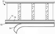
除了示出密封层(28)的细节之外,图6还示出了如何将光准直层(10)层压到诸如玻璃或另一种透明耐用材料的基板(53)上。尽管在图6中未示出,但是注意,可以用基板在顶部和底部上保护光准直层(10)。两个基板可以不同或相同,例如,第一基板可以是玻璃,而第二基板可以是聚乙烯。边缘密封件(51)可以围绕顶部和底部基板以及基板之间的光准直层(10)延伸。通常,光学粘合剂(52)(例如可从Delo Adhesives获得)用于将光准直层(10)粘合到基板(53)上。可替代地,可以用光学粘合剂(52)和释放片(54)的组合涂布光准直层(10),从而可以将具有释放片(54)的光准直层(10)卷起,并运输到装配厂,将其切成一定尺寸。如图7所示,在展开之前,可以移除释放片(54),并且可以将光准直层(10)直接附接到基板(53)上。基板可以是期望光准直的任何透明表面,例如会议室窗户、汽车玻璃或LCD堆叠中的扩散器。In addition to showing details of the sealing layer (28), Figure 6 also shows how the light collimating layer (10) is laminated to a substrate (53) such as glass or another transparent durable material. Although not shown in Figure 6, note that the light collimating layer (10) can be protected on the top and bottom with a substrate. The two substrates may be different or the same, for example, the first substrate may be glass and the second substrate may be polyethylene. An edge seal (51) may extend around the top and bottom substrates and the light collimating layer (10) between the substrates. Typically, an optical adhesive (52), such as available from Delo Adhesives, is used to bond the light-collimating layer (10) to the substrate (53). Alternatively, the light-collimating layer (10) can be coated with a combination of an optical adhesive (52) and a release sheet (54) so that the light-collimating layer (10) with the release sheet (54) can be rolled up , and transported to an assembly plant where it is cut to size. As shown in Figure 7, prior to deployment, the release sheet (54) can be removed and the light-collimating layer (10) can be attached directly to the substrate (53). The substrate can be any transparent surface where light collimation is desired, such as conference room windows, automotive glass, or diffusers in LCD stacks.
制造光准直层Fabrication of light-collimating layers
可以使用如图8所示并在US 9,081,250中详细描述的卷对卷工艺来生产光准直膜。如图8所示,该工艺涉及多个步骤:在第一步骤中,将压印组合物(例如热塑性塑料、热固性塑料或其前体)的层(60),可选地与溶剂一起,沉积在导电透明膜(61)上,导电透明膜例如包括氧化铟锡层的聚对苯二甲酸乙二酯(PET)(PET-ITO)膜。(如果存在溶剂,则溶剂容易挥发)。底漆层(即,电极保护层)可以用于增加压印组合物层与支撑层(其可以是PET)之间的粘合力。另外,可以在底漆层中使用助粘剂以改善与支撑层的粘合力。在第二步骤中,通过预图案化的压印工具(62)在高于层材料的玻璃化转变温度的温度下压印层(60),其制造在下面描述。(可以调节底漆和/或助粘剂以减少与压印工具(62)的粘合力。)在第三步骤中,优选地在例如通过冷却硬化期间或之后从压印工具(62)释放图案化的层(60)。现在建立了细长腔室的特征图案(如上所述)。在步骤四中,细长腔室(63)填充有上述的双稳态电泳流体(64)。在一些实施例中,双稳态电泳流体将包括与电泳流体(64)不相容并且比重小于电泳流体(64)中的溶剂和颜料粒子的密封组合物。在这样的实施例中,密封组合物将上升到细长腔室(63)的顶部,从而可以在随后的步骤中硬化。作为替代方案(图8中未示出),可以在细长腔室(63)被填充电泳流体(64)之后外敷密封组合物。在下一步骤中,通过用例如UV辐射(65)、或通过热或水分硬化密封组合物来密封填充有电泳流体(64)的细长腔室(63)。在第六步骤中,将密封的细长腔室层压到第二透明导电膜(66),该第二透明导电膜可以预涂布有光学透明粘合剂层(67),该粘合剂可以是压敏粘合剂、热熔性胶粘剂、热、水分或辐射可固化的粘合剂。[用于光学透明粘合剂的优选材料包括丙烯酸、苯乙烯-丁二烯共聚物、苯乙烯-丁二烯-苯乙烯嵌段共聚物、苯乙烯-异戊二烯-苯乙烯嵌段共聚物、聚乙烯醇缩丁醛、乙酸丁酸纤维素、聚乙烯吡咯烷酮、聚氨酯、聚酰胺、乙烯-乙酸乙烯酯共聚物、环氧化物、多官能丙烯酸酯、乙烯基、乙烯基醚及其低聚物、聚合物和共聚物。]在最后的步骤中,例如可以用刀刃(69)或用激光切割机来切割完成的可切换的光准直膜片。在一些实施例中,可以在完成的可切换的光准直膜上执行第八步骤,其包括层压另一种光学透明的粘合剂和释放片,以使得该膜可以以切片或卷运输并在使用时切割成一定尺寸,例如用于结合到显示器、窗户或其他装置/基板中。The light-collimating film can be produced using a roll-to-roll process as shown in Figure 8 and described in detail in US 9,081,250. As shown in Figure 8, the process involves multiple steps: In a first step, a layer (60) of an imprinting composition (eg thermoplastic, thermoset or precursor thereof), optionally together with a solvent, is deposited On the conductive transparent film (61), a conductive transparent film such as a polyethylene terephthalate (PET) (PET-ITO) film including an indium tin oxide layer. (If a solvent is present, the solvent is easily volatile). The primer layer (ie, the electrode protection layer) can be used to increase the adhesion between the imprint composition layer and the support layer (which can be PET). Additionally, adhesion promoters can be used in the primer layer to improve adhesion to the support layer. In a second step, the layer (60) is imprinted by a pre-patterned imprint tool (62) at a temperature above the glass transition temperature of the layer material, the fabrication of which is described below. (The primer and/or adhesion promoter may be adjusted to reduce adhesion to the imprint tool (62).) In a third step, release from the imprint tool (62) is preferably performed during or after hardening, for example by cooling Patterned layer (60). The characteristic pattern of elongated chambers is now established (as described above). In step four, the elongated chamber (63) is filled with the above-mentioned bistable electrophoretic fluid (64). In some embodiments, the bistable electrophoretic fluid will include a sealing composition that is incompatible with the electrophoretic fluid (64) and has a specific gravity less than the solvent and pigment particles in the electrophoretic fluid (64). In such an embodiment, the sealing composition will rise to the top of the elongated chamber (63) so that it can harden in a subsequent step. As an alternative (not shown in Figure 8), the sealing composition may be topically applied after the elongated chamber (63) is filled with the electrophoretic fluid (64). In the next step, the elongated chamber (63) filled with electrophoretic fluid (64) is sealed by hardening the sealing composition with eg UV radiation (65), or by heat or moisture. In a sixth step, the sealed elongated chamber is laminated to a second transparent conductive film (66), which may be pre-coated with a layer of optically clear adhesive (67), the adhesive Can be pressure sensitive adhesives, hot melt adhesives, heat, moisture or radiation curable adhesives. [Preferred materials for optically clear adhesives include acrylic, styrene-butadiene copolymer, styrene-butadiene-styrene block copolymer, styrene-isoprene-styrene block copolymer compounds, polyvinyl butyral, cellulose acetate butyrate, polyvinyl pyrrolidone, polyurethane, polyamide, ethylene-vinyl acetate copolymer, epoxide, polyfunctional acrylate, vinyl, vinyl ether and its low polymers, polymers and copolymers. ] In a final step, the finished switchable light-collimating film can be cut, for example, with a knife edge (69) or with a laser cutter. In some embodiments, the eighth step can be performed on the finished switchable light-collimating film, which includes laminating another optically clear adhesive and a release sheet, so that the film can be shipped in slices or rolls And cut to size when in use, for example for incorporation into displays, windows or other devices/substrates.
可以通过光阻工艺,随后通过蚀刻或电镀来制备压印工具(62)。然后将其涂布一层光阻并暴露在UV下。将掩模放置在UV和光阻层之间。在一些实施例中,然后通过用适当的有机溶剂或水溶液清洗来移除未暴露或暴露的区域。干燥剩余的光阻,并再次用种子金属薄层溅射。然后,母版准备好进行电铸。用于电铸的典型材料是镍钴。可替代地,母版可以通过氨基磺酸镍电铸或无电镍沉积,而由镍所制成。压印工具的底板通常为50至5000微米厚。母版也可以使用其他微工程技术制成,包括电子束(e-beam)写入、干法蚀刻、化学蚀刻、激光写入或激光干涉,如“Replication techniques for micro-optics”,SPIEProc.Vol.3099,pp 76-82(1997)中所述。可替代地,压印工具可以通过使用塑料、陶瓷或金属的光加工来制造。下面更详细地描述用于压印工具生产的几种方法。The imprint tool (62) may be prepared by a photoresist process followed by etching or electroplating. It is then coated with a layer of photoresist and exposed to UV. A mask is placed between the UV and photoresist layers. In some embodiments, unexposed or exposed areas are then removed by washing with a suitable organic solvent or aqueous solution. Dry the remaining photoresist and sputter again with a thin layer of seed metal. The master is then ready for electroforming. A typical material for electroforming is nickel cobalt. Alternatively, the master can be made of nickel by nickel sulfamate electroforming or electroless nickel deposition. The base plate of the imprint tool is typically 50 to 5000 microns thick. Masters can also be made using other micro-engineering techniques, including electron beam (e-beam) writing, dry etching, chemical etching, laser writing or laser interference, such as "Replication techniques for micro-optics", SPIEProc.Vol .3099, pp 76-82 (1997). Alternatively, the embossing tool can be manufactured by photoprocessing using plastic, ceramic or metal. Several methods for imprint tool production are described in more detail below.
图9A和9B示出了具有压印工具(111)的压印工艺,该压印工具在其表面上具有三维微结构(圆圈)。如图9A和9B所示,在将压印工具(111)施加到至少20μm厚,例如至少40μm厚、例如至少50μm厚、例如至少60μm厚、例如至少80μm厚、例如至少100μm厚、例如至少150μm、例如至少200μm厚、例如至少250μm厚的压印组合物(112)之后。在压印组合物固化(例如,通过辐射)或热压印材料通过热和压力压印之后,压印材料从压印工具中释放出来(参见图9B),留下所需尺寸的细长腔室,例如,其中细长腔室的高度等于或小于准直层(压印组合物)的厚度,以及其中,细长腔室的宽度在9μm和150μm之间,并且腔室的长度在200μm和5mm之间。Figures 9A and 9B show an imprinting process with an imprinting tool (111) having three-dimensional microstructures (circles) on its surface. As shown in Figures 9A and 9B, after applying the imprint tool (111) to a thickness of at least 20 μm, such as at least 40 μm thick, such as at least 50 μm thick, such as at least 60 μm thick, such as at least 80 μm thick, such as at least 100 μm thick, such as at least 150 μm thick , for example at least 200 μm thick, for example at least 250 μm thick imprinting composition (112). After the imprinting composition is cured (eg, by radiation) or the thermal imprinting material is imprinted by heat and pressure, the imprinting material is released from the imprinting tool (see Figure 9B), leaving an elongated cavity of desired size chamber, for example, wherein the height of the elongated chamber is equal to or less than the thickness of the alignment layer (imprint composition), and wherein the width of the elongated chamber is between 9 μm and 150 μm and the length of the chamber is between 200 μm and 200 μm between 5mm.
使用常规的压印工具,由于固化或热压印材料与压印工具的表面之间的不期望的强粘合力,因此固化或热压印材料有时不能从工具中完全释放。在这种情况下,可能会有一些固化或热压印材料转移到或粘在压印工具的表面上,使得在由该工艺形成的物体上留下不平坦的表面。Using conventional embossing tools, the cured or hot embossed material sometimes cannot be fully released from the tool due to undesirably strong adhesion between the cured or hot embossed material and the surface of the embossing tool. In this case, some of the cured or hot embossing material may transfer or stick to the surface of the embossing tool, leaving an uneven surface on the object formed by the process.
如果物体形成在诸如透明导电层或聚合物层的支撑层上,则该问题更加明显。如果固化或热压印材料与支撑层之间的粘合力比固化或热压印材料与压印工具表面之间的粘合力弱,则固化或热压印材料从压印工具的释放过程可能会导致物体与支撑层分离。This problem is more pronounced if the object is formed on a support layer such as a transparent conductive layer or a polymer layer. If the adhesion between the cured or hot embossed material and the support layer is weaker than the adhesion between the cured or hot embossed material and the surface of the embossing tool, the release process of the cured or hot embossed material from the embossing tool May cause objects to separate from the support layer.
在某些情况下,可以在层的堆叠上形成物体。在这种情况下,如果任意两个相邻层之间的粘合力比固化或热压印材料与压印工具表面之间的粘合力弱,则固化或热压印材料从压印工具的释放过程可能导致两个层之间的破裂。In some cases, objects may be formed on stacks of layers. In this case, if the adhesion between any two adjacent layers is weaker than the adhesion between the cured or hot embossed material and the surface of the imprinting tool, the cured or hot embossed material is removed from the imprinting tool The release process may lead to rupture between the two layers.
当固化压印组合物或热压印材料没有很好地粘附于某些支撑层时,上述问题尤其令人关注。例如,如果支撑层是聚合物层,在聚合物层和固化或热压印的压印组合物之一是亲水的而另一个是疏水的情况下,则在聚合物层与固化或热压印的压印组合物之间的粘合力很弱。因此,优选地,压印组合物和支撑层都是疏水的或都是亲水的。The above problems are of particular concern when cured imprint compositions or hot imprint materials do not adhere well to certain support layers. For example, if the support layer is a polymer layer, in the case where one of the polymer layer and the cured or heat-embossed imprinting composition is hydrophilic and the other is hydrophobic, the The adhesion between the imprinted imprinting compositions was weak. Therefore, preferably, both the imprinting composition and the support layer are hydrophobic or both are hydrophilic.
用于形成压印层或支撑层的合适的亲水性组合物可以包含极性低聚物或聚合物材料。如美国专利No.7,880,958中所述,这种极性低聚物或聚合物材料可以选自由具有以下至少一种基团的低聚物或聚合物组成的组,该基团例如硝基(-NO2)、羟基(-OH)、羧基(-COO)、烷氧基(-OR,其中R是烷基)、卤素(例如,氟、氯、溴或碘)、氰基(-CN)、磺酸基(-SO3)等。极性聚合物材料的玻璃化转变温度优选地低于约100℃,以及更优选低于约60℃。合适的极性低聚物或聚合物材料的具体示例可以包括但不限于聚乙烯醇、聚丙烯酸、聚(2-甲基丙烯酸二甲胺乙酯)、多羟基官能化的聚酯丙烯酸酯(例如BDE 1025,康涅狄格州温斯特市(Winsted,CT)的Bomar Specialties Co)或烷氧基化丙烯酸酯,例如乙氧基壬基酚丙烯酸酯(例如,SR504,美国沙多玛公司(Sartomer Company))、乙氧基化三羟甲基丙烷三丙烯酸酯(例如,SR9035,美国沙多玛公司)或乙氧基季戊四醇四丙烯酸酯(例如,SR494,来自美国沙多玛公司)。Suitable hydrophilic compositions for forming the imprint or support layer may comprise polar oligomeric or polymeric materials. As described in US Pat. No. 7,880,958, such polar oligomeric or polymeric materials may be selected from the group consisting of oligomers or polymers having at least one group such as a nitro (- NO2 ), hydroxyl (-OH), carboxyl (-COO), alkoxy (-OR, where R is alkyl), halogen (eg, fluorine, chlorine, bromine, or iodine), cyano (-CN), Sulfonic acid group (-SO3 ) and the like. The glass transition temperature of the polar polymeric material is preferably below about 100°C, and more preferably below about 60°C. Specific examples of suitable polar oligomeric or polymeric materials may include, but are not limited to, polyvinyl alcohol, polyacrylic acid, poly(dimethylamine ethyl 2-methacrylate), polyhydroxy-functional polyester acrylates ( For example, BDE 1025, Bomar Specialties Co, Winsted, CT) or alkoxylated acrylates, such as ethoxylated nonylphenol acrylate (eg, SR504, Sartomer Company )), ethoxylated trimethylolpropane triacrylate (eg, SR9035 from Sartomer, USA) or ethoxylated pentaerythritol tetraacrylate (eg, SR494 from Sartomer, USA).
压印工具(111)可直接用于将组合物(112)压印。更典型地,压印工具(111)安装在平直滚筒上,以允许压印套筒在压印组合物(112)上旋转。压印滚筒或套筒(121)通常由导电材料形成,导电材料例如金属(例如,铝、铜、锌、镍、铬、铁、钛、钴等)、由上述任一种金属衍生的合金、或不锈钢。可以使用不同的材料来形成滚筒或套筒。例如,滚筒或套筒的中心可以由不锈钢形成,并且镍层被夹在不锈钢和最外层之间,该最外层可以是铜层。The embossing tool (111) can be used directly to emboss the composition (112). More typically, the stamping tool (111) is mounted on a flat cylinder to allow the stamping sleeve to rotate on the stamping composition (112). The impression cylinder or sleeve (121) is typically formed of a conductive material such as a metal (eg, aluminum, copper, zinc, nickel, chromium, iron, titanium, cobalt, etc.), alloys derived from any of the foregoing, or stainless steel. Different materials can be used to form the drum or sleeve. For example, the center of the drum or sleeve can be formed of stainless steel, and the nickel layer is sandwiched between the stainless steel and the outermost layer, which can be a copper layer.
方法A:如图10所示,压印滚筒或套筒(121)可以由在其外表面上具有导电涂层或导电种子层的非导电材料形成。如图10的步骤B所示,在将感光材料(122)涂布在滚筒或套筒(21)的外表面上之前,可以使用精密研磨和抛光以确保滚筒或套筒的外表面的光滑度。然后可以将例如光阻的感光材料(122)涂布在滚筒或套筒(121)的外表面上。感光材料可以是正性、负性或双性。感光材料也可以是化学放大光阻。可以使用浸涂、喷涂或环涂进行涂布。在干燥和/或烘烤之后,可以使感光材料经历曝光,如图10的步骤C所示,例如,通过将感光材料暴露于光源。可替代地,感光材料(122)可以是层压到滚筒或套筒(121)的外表面上的干膜光阻。当使用干膜时,也如上所述暴露于光源。Method A: As shown in Figure 10, the impression cylinder or sleeve (121) may be formed of a non-conductive material with a conductive coating or conductive seed layer on its outer surface. As shown in step B of Figure 10, before coating the photosensitive material (122) on the outer surface of the drum or sleeve (21), precision grinding and polishing can be used to ensure the smoothness of the outer surface of the drum or sleeve (21). . A photosensitive material (122), such as photoresist, can then be coated on the outer surface of the drum or sleeve (121). Photosensitive materials can be positive, negative, or bisexual. The photosensitive material can also be a chemically amplified photoresist. Coating can be done using dip coating, spray coating or ring coating. After drying and/or baking, the photosensitive material may be subjected to exposure, as shown in step C of Figure 10, for example, by exposing the photosensitive material to a light source. Alternatively, the photosensitive material (122) may be a dry film photoresist laminated to the outer surface of the drum or sleeve (121). When dry film is used, it is also exposed to the light source as described above.
在图10的步骤C中,合适的光源(123),例如红外线(IR)、UV、电子束或激光,用于曝光在滚筒或套筒(121)上涂布的感光材料或层压的干膜光阻(122)。光源可以是连续光或脉冲光。光掩模(124)可选地用于限定要形成的三维微结构。取决于微结构,曝光可以是逐步的、连续的或其组合。在曝光之后,可以在显影之前对感光材料(122)进行曝光后处理,例如烘烤。取决于感光材料的特征,将通过使用显影剂移除曝光或未曝光的区域。在显影之后,在沉积(例如电镀、无电镀、物理气相沉积、化学气相沉积或溅射沉积)之前,可以将在其外表面上具有图案化的感光材料(125)的滚筒或套筒(如图10的步骤D所示)进行烘烤或全面曝光。图案化的感光材料的厚度优选地大于要形成的三维微结构的深度或高度。In step C of Figure 10, a suitable light source (123), such as infrared (IR), UV, electron beam or laser, is used to expose the photosensitive material or laminated dry material coated on the drum or sleeve (121). Film photoresist (122). The light source can be continuous light or pulsed light. A photomask (124) is optionally used to define the three-dimensional microstructure to be formed. Depending on the microstructure, exposure can be stepwise, continuous, or a combination thereof. After exposure, the photosensitive material (122) may be subjected to post-exposure processing, such as baking, prior to development. Depending on the characteristics of the photosensitive material, exposed or unexposed areas will be removed by using a developer. After development, prior to deposition (eg, electroplating, electroless plating, physical vapor deposition, chemical vapor deposition, or sputter deposition), a roller or sleeve (eg, a photosensitive material (125) patterned on its outer surface) may be As shown in step D of FIG. 10), baking or full exposure is performed. The thickness of the patterned photosensitive material is preferably greater than the depth or height of the three-dimensional microstructure to be formed.
可以将金属或合金(例如,镍、钴、铬、铜、锌或衍生自任何上述金属的合金)电镀和/或无电镀在滚筒或套筒上。镀覆材料(126)沉积在滚筒或套筒的外表面上未被图案化的感光材料覆盖的区域中。沉积物厚度优选地小于感光材料的厚度,如图10的步骤E所示。通过调节镀覆条件,例如,阳极和阴极(即,滚筒或套筒)之间的距离(如果使用电镀)、滚筒或套筒的转速和/或镀液的循环,可以将整个滚筒或套筒区域上的沉积物的厚度变化控制为小于1%。Metals or alloys (eg, nickel, cobalt, chromium, copper, zinc, or alloys derived from any of the foregoing metals) may be electroplated and/or electroless plated on the drum or sleeve. A plating material (126) is deposited on the outer surface of the drum or sleeve in areas not covered by the patterned photosensitive material. The thickness of the deposit is preferably smaller than the thickness of the photosensitive material, as shown in step E of FIG. 10 . By adjusting the plating conditions, such as the distance between the anode and cathode (ie, the drum or sleeve) (if electroplating is used), the rotational speed of the drum or sleeve, and/or the circulation of the bath, the entire drum or sleeve can be The thickness variation of the deposit on the area is controlled to be less than 1%.
可替代地,在使用电镀来沉积镀覆材料(126)的情况下,可以通过在阴极(即,滚筒或套筒)和阳极之间插入非导电的厚度变流机(uniformer)来控制沉积物在整个滚筒或套筒表面上的厚度变化,如美国专利No.8,114,262中所描述的,其全部内容通过引用包含于此。Alternatively, where electroplating is used to deposit the plating material (126), the deposition can be controlled by inserting a non-conductive thickness uniformer between the cathode (ie, drum or sleeve) and the anode Thickness variation across the surface of the drum or sleeve, as described in US Patent No. 8,114,262, the entire contents of which are incorporated herein by reference.
在镀覆之后,可以通过剥离剂(例如,有机溶剂或水溶液)剥离图案化的感光材料(125)。可以可选地使用精密抛光,以确保整个滚筒或套筒上的沉积物(126)的厚度变化和粗糙度是可接受的。图10的步骤F示出了其上形成有三维图案微结构的压印滚筒或套筒的横截面图。After plating, the patterned photosensitive material (125) can be stripped by a stripper (eg, organic solvent or aqueous solution). Precision polishing may optionally be used to ensure acceptable thickness variation and roughness of the deposit (126) across the drum or sleeve. Step F of Figure 10 shows a cross-sectional view of an impression cylinder or sleeve with a three-dimensional patterned microstructure formed thereon.
方法B:可替代地,如图11所示,可以在平坦的基板上形成三维微结构。在图11的步骤A中,将感光材料(142)涂布在基板层(141)(例如,玻璃基板)上。如上所述,感光材料(142)可以是正性、负性或双性。感光材料(142)也可以是化学放大光阻。可以使用浸涂、喷涂、狭缝挤压式涂布或旋转涂布进行涂布。在干燥和/或烘烤之后,使感光材料通过光掩模(未示出)暴露于合适的光源(未示出)。可替代地,感光材料(142)可以是层压到基板(141)上的干膜光阻(其通常是可商购获得的)。如上所述,干膜也暴露于光源。Method B: Alternatively, as shown in Figure 11, three-dimensional microstructures can be formed on a flat substrate. In step A of Figure 11, a photosensitive material (142) is coated on a substrate layer (141) (eg, a glass substrate). As mentioned above, the photosensitive material (142) can be positive, negative, or bisexual. The photosensitive material (142) can also be a chemically amplified photoresist. Coating can be done using dip coating, spray coating, slot coating or spin coating. After drying and/or baking, the photosensitive material is exposed to a suitable light source (not shown) through a photomask (not shown). Alternatively, the photosensitive material (142) may be a dry film photoresist (which is typically commercially available) laminated to the substrate (141). As mentioned above, the dry film is also exposed to the light source.
在图11的步骤B中,在曝光之后,取决于感光材料的特征,将通过使用显影剂移除感光材料的曝光或未曝光的区域。在显影之后,在步骤C之前,可以将具有剩余的感光材料(142)的基板层(141)进行烘烤或全面曝光。剩余的感光材料的厚度应该与要形成的三维微结构的深度或高度相同。在步骤C中,在剩余的感光材料(142)和基板(141)未被感光材料占据的区域上涂布导电种子层(143)。导电种子层通常由银形成;然而,也可以使用其他导电材料,例如金或镍。In step B of FIG. 11, after exposure, the exposed or unexposed areas of the photosensitive material will be removed by using a developer, depending on the characteristics of the photosensitive material. After development, before step C, the substrate layer (141) with the remaining photosensitive material (142) may be baked or fully exposed. The thickness of the remaining photosensitive material should be the same as the depth or height of the three-dimensional microstructure to be formed. In step C, a conductive seed layer (143) is coated on the remaining photosensitive material (142) and the areas of the substrate (141) not occupied by the photosensitive material. The conductive seed layer is typically formed of silver; however, other conductive materials such as gold or nickel can also be used.
在步骤D中,将金属或合金(144)(例如,镍、钴、铬、铜、锌或衍生自任何上述金属的合金)电镀和/或无电镀在被导电种子层覆盖的表面上,并且直到在图案化的感光材料上有足够的镀覆材料厚度(h),才停止执行镀覆工艺。图11的步骤D中的厚度(h)优选地为25至5000微米,以及更优选地为25至1000微米。In step D, a metal or alloy (144) (eg, nickel, cobalt, chromium, copper, zinc, or an alloy derived from any of the foregoing metals) is electroplated and/or electroless plated on the surface covered by the conductive seed layer, and The plating process is not stopped until there is sufficient plating material thickness (h) on the patterned photosensitive material. The thickness (h) in step D of FIG. 11 is preferably 25 to 5000 micrometers, and more preferably 25 to 1000 micrometers.
在镀覆之后,将镀覆材料(144)与被剥离的基板层(141)分离。移除感光材料(142)以及导电种子层(143)。可以通过剥离剂(例如,有机溶剂或水溶液)移除感光材料。可以通过酸性溶液(例如,硫酸/硝酸混合物)或可商购获得的化学剥离剂移除导电种子层(143),仅留下一侧具有三维结构且另一侧平坦的金属片(144)。可以对金属片(144)施加精密抛光,在精密抛光之后,平垫片可以直接用于压印,或者将其安装在(即缠绕在)外表面上具有三维微结构的滚筒上以形成压印工具。如上所述,最终将贵金属或其合金涂布在压印工具的整个表面上。如上所述,由于金或其合金缺乏反应性,因此比其他贵金属和合金更优选。After plating, the plating material (144) is separated from the stripped substrate layer (141). The photosensitive material (142) and the conductive seed layer (143) are removed. The photosensitive material can be removed by a stripper (eg, organic solvent or aqueous solution). The conductive seed layer (143) can be removed by an acidic solution (eg, a sulfuric/nitric acid mixture) or a commercially available chemical stripper, leaving only a metal sheet (144) with three-dimensional structure on one side and flat on the other. The metal sheet (144) can be precision polished, after which the flat gasket can be used directly for imprinting, or it can be mounted (ie wrapped around) on a cylinder with three-dimensional microstructures on the outer surface to form the imprint tool. As mentioned above, the precious metal or its alloy is finally coated on the entire surface of the imprint tool. As mentioned above, gold or its alloys are preferred over other noble metals and alloys due to their lack of reactivity.
方法C:在图12中示出了另一种替代方法。该方法类似于图11的方法,但被简化。代替诸如银的导电种子层,将贵金属或其合金层(153)简单地涂布在感光材料(152)上。如上所述,金或其合金是优选的。因此,在步骤E中,在将镀覆材料(154)与基板(151)分离之后,仅移除感光材料(152),金或合金涂层(153)与一侧具有三维结构且另一侧平坦的金属片(154)则一起保留。Method C: Another alternative method is shown in FIG. 12 . This method is similar to that of Figure 11, but simplified. Instead of a conductive seed layer such as silver, a layer of noble metal or its alloy (153) is simply coated on the photosensitive material (152). As mentioned above, gold or alloys thereof are preferred. Therefore, in step E, after separating the plating material (154) from the substrate (151), only the photosensitive material (152) is removed, the gold or alloy coating (153) has a three-dimensional structure with one side and the other side The flat metal sheet (154) remains together.
用于形成准直层的组合物中的组分的示例可以包括但不限于热塑性或热固性材料或其前体,例如多官能乙烯基,包括但不限于丙烯酸酯、甲基丙烯酸酯,烯丙基、乙烯基苯、乙烯基醚、多官能环氧化物及其低聚物或聚合物等。经常使用多官能丙烯酸酯及其低聚物。多官能环氧化物和多官能丙烯酸酯的组合也用于获得准直层的期望的物理机械性能。还可以添加低Tg(玻璃化转变温度)粘结剂或赋予柔性的可交联低聚物,例如聚氨酯丙烯酸酯或聚酯丙烯酸酯,以改善压印防窥层的抗弯曲性。Examples of components in the composition used to form the alignment layer may include, but are not limited to, thermoplastic or thermoset materials or precursors thereof, such as multifunctional vinyls, including but not limited to acrylates, methacrylates, allyls , vinylbenzene, vinyl ether, multifunctional epoxides and their oligomers or polymers. Multifunctional acrylates and their oligomers are often used. Combinations of multifunctional epoxides and multifunctional acrylates are also used to obtain the desired physico-mechanical properties of the alignment layer. Low Tg (glass transition temperature) binders or crosslinkable oligomers imparting flexibility, such as urethane acrylates or polyester acrylates, can also be added to improve the flex resistance of the imprint privacy layer.
用于准直层的组合物的其他示例可以包括极性低聚物或聚合物材料。这样的极性低聚物或聚合物材料可以选自由具有以下至少一种基团的低聚物或聚合物组成的组,该基团例如硝基(-NO2)、羟基(-OH)、羧基(-COO)、烷氧基(-OR,其中R是烷基)、卤素(例如,氟、氯、溴或碘)、氰基(-CN)、磺酸基(-SO3)等。极性聚合物材料的玻璃化转变温度优选地低于约100℃,以及更优选低于约60℃。合适的极性低聚物或聚合物材料的具体示例可以包括但不限于多羟基官能化的聚酯丙烯酸酯(例如BDE1025,康涅狄格州温斯特市(Winsted,CT)的Bomar Specialties Co)或烷氧基化丙烯酸酯,例如乙氧基壬基酚丙烯酸酯(例如,SR504,美国沙多玛公司)、乙氧基化三羟甲基丙烷三丙烯酸酯(例如,SR9035,美国沙多玛公司)或乙氧基化季戊四醇四丙烯酸酯(例如,SR494,来自美国沙多玛公司)。Other examples of compositions for alignment layers may include polar oligomeric or polymeric materials. Such polar oligomeric or polymeric materials may be selected from the group consisting of oligomers or polymers having at least one group such as nitro (-NO2 ), hydroxyl (-OH), Carboxyl (-COO), alkoxy (-OR, where R is an alkyl group), halogen (eg, fluorine, chlorine, bromine, or iodine), cyano (-CN), sulfonic acid (-SO3 ), and the like. The glass transition temperature of the polar polymeric material is preferably below about 100°C, and more preferably below about 60°C. Specific examples of suitable polar oligomeric or polymeric materials may include, but are not limited to, polyhydroxy-functionalized polyester acrylates (eg, BDE1025, Bomar Specialties Co, Winsted, CT) or alkanes. Oxylated acrylates such as ethoxylated nonylphenol acrylate (eg, SR504, Sartomer, USA), ethoxylated trimethylolpropane triacrylate (eg, SR9035, Sartomer, USA) Or ethoxylated pentaerythritol tetraacrylate (eg, SR494 from Sartomer, USA).
可替代地,准直层组合物可以包括(a)至少一种双官能UV可固化的组分,(b)至少一种光引发剂,和(c)至少一种脱模剂。合适的双官能组分可以具有高于约200的分子量。双官能丙烯酸酯是优选的,并且具有氨基甲酸乙酯或乙氧基主链的双官能丙烯酸酯是特别优选的。更具体地,合适的双官能组分可以包括但不限于二乙二醇二丙烯酸酯(例如,来自沙多玛的SR230)、三乙二醇二丙烯酸酯(例如,来自沙多玛的SR272)、四乙二醇二丙烯酸酯(例如,来自沙多玛的SR268)、聚乙二醇二丙烯酸酯(例如,来自沙多玛的SR295、SR344或SR610)、聚乙二醇二甲基丙烯酸酯(例如,来自沙多玛的SR603、SR644、SR252或SR740)、乙氧基化双酚A二丙烯酸酯(例如,来自沙多玛的CD9038、SR349、SR601或SR602)、乙氧基化双酚A二甲基丙烯酸酯(例如,来自沙多玛的CD540、CD542、SR101、SR150、SR348、SR480或SR541)、和氨基甲酸酯二丙烯酸酯(例如,来自沙多玛的CN959、CN961、CN964、CN965、CN980或CN981;来自美国氰特(Cytec)的Ebecryl 230、Ebecryl 270、Ebecryl 8402、Ebecryl 8804、Ebecryl 8807或Ebecryl 8808)。合适的光引发剂可以包括但不限于双酰基氧化膦、2-苄基-2-(二甲氨基)-1-[4-(4-吗啉基)苯基]-1-丁酮、2,4,6-三甲基苯甲酰二苯氧化膦、2-异丙基-9H-噻吨-9-酮、4-苯甲酰基-4'-甲基二苯硫醚和1-羟基-环己基-苯基酮、2-羟基-2-甲基-1-苯基-丙烷-1-酮、1-[4-(2-羟基乙氧基)-苯基]-2-羟基-2-甲基-1-丙烷-1-酮、2,2-二甲氧基-1,2-二苯基乙烷-1-酮或2-甲基-1[4-(甲硫基)苯基]-2-吗啉丙烷-1-酮。合适的脱模剂可以包括但不限于有机改性的有机硅共聚物,例如有机硅丙烯酸酯(例如,来自美国氰特的Ebercryl 1360或Ebercyl 350)、有机硅聚醚(例如,来自迈图(Momentive)的Silwet 7200、Silwet 7210、Silwet 7220、Silwet 7230、Silwet 7500、Silwet 7600或Silwet 7607)。所述组合物可以进一步可选地包含一种或多种以下组分,共引发剂、单官能UV可固化的组分、多官能UV可固化的组分或稳定剂。Alternatively, the alignment layer composition may include (a) at least one bifunctional UV-curable component, (b) at least one photoinitiator, and (c) at least one mold release agent. Suitable bifunctional components can have molecular weights above about 200. Difunctional acrylates are preferred, and difunctional acrylates having a urethane or ethoxy backbone are particularly preferred. More specifically, suitable bifunctional components may include, but are not limited to, diethylene glycol diacrylate (eg, SR230 from Sartomer), triethylene glycol diacrylate (eg, SR272 from Sartomer) , tetraethylene glycol diacrylate (eg, SR268 from Sartomer), polyethylene glycol diacrylate (eg, SR295, SR344, or SR610 from Sartomer), polyethylene glycol dimethacrylate (eg, SR603, SR644, SR252, or SR740 from Sartomer), ethoxylated bisphenol A diacrylate (eg, CD9038, SR349, SR601, or SR602 from Sartomer), ethoxylated bisphenol A Dimethacrylates (eg, CD540, CD542, SR101, SR150, SR348, SR480, or SR541 from Sartomer), and urethane diacrylates (eg, CN959, CN961, CN964 from Sartomer , CN965, CN980 or CN981; Ebecryl 230, Ebecryl 270, Ebecryl 8402, Ebecryl 8804, Ebecryl 8807 or Ebecryl 8808 from Cytec). Suitable photoinitiators may include, but are not limited to, bisacylphosphine oxide, 2-benzyl-2-(dimethylamino)-1-[4-(4-morpholinyl)phenyl]-1-butanone, 2- ,4,6-Trimethylbenzoyldiphenylphosphine oxide, 2-isopropyl-9H-thioxanthene-9-one, 4-benzoyl-4'-methyldiphenyl sulfide and 1-hydroxyl -Cyclohexyl-phenyl ketone, 2-hydroxy-2-methyl-1-phenyl-propan-1-one, 1-[4-(2-hydroxyethoxy)-phenyl]-2-hydroxy- 2-Methyl-1-propan-1-one, 2,2-dimethoxy-1,2-diphenylethan-1-one or 2-methyl-1[4-(methylthio) Phenyl]-2-morpholinopropan-1-one. Suitable release agents may include, but are not limited to, organically modified silicone copolymers such as silicone acrylates (eg, Ebercryl 1360 or Ebercyl 350 from Cytec, USA), silicone polyethers (eg, from Momentive ( Momentive's Silwet 7200, Silwet 7210, Silwet 7220, Silwet 7230, Silwet 7500, Silwet 7600 or Silwet 7607). The composition may further optionally comprise one or more of the following components, a co-initiator, a monofunctional UV curable component, a multifunctional UV curable component, or a stabilizer.
细长腔室的设置Setup of the elongated chamber
图13和14示出了由上述制造方法产生的光准直层的两种几何形状(从上方观看)。这些几何形状示出了细长腔室(22)的纵横比的总体趋势为它们在一个方向(L)上比另一个方向(W)更长。也就是说,细长腔室的长度(L)通常是细长腔室的宽度(W)的至少两倍,例如是细长腔室的宽度的至少三倍、例如是细长腔室的宽度的至少四倍、例如是细长腔室的宽度的至少五倍、例如是细长腔室的宽度的至少十倍。[如以上所讨论的,细长腔室的高度(H)(在图13和14中的页面平面之外)等于或小于准直层的厚度。]通常,每个细长腔室的宽度在9μm至150μm之间。通常,每个细长腔室的长度在200μm至5mm之间。Figures 13 and 14 show two geometries (viewed from above) of the light-collimating layer produced by the above-described fabrication method. These geometries show a general trend of the aspect ratios of the elongated chambers (22) as they are longer in one direction (L) than the other (W). That is, the length (L) of the elongated chamber is typically at least twice the width (W) of the elongated chamber, such as at least three times the width of the elongated chamber, such as the width of the elongated chamber is at least four times the width of the elongated chamber, such as at least five times the width of the elongated chamber, such as at least ten times the width of the elongated chamber. [As discussed above, the height (H) of the elongated chamber (outside the plane of the page in Figures 13 and 14) is equal to or less than the thickness of the collimation layer. ] Typically, the width of each elongated chamber is between 9 μm and 150 μm. Typically, the length of each elongated chamber is between 200 μm and 5 mm.
如前所讨论的,当电泳颜料(26)完全分布在细长腔室(22)中时,行之间的间隔(A)(又称“节距”)在确定减小多少视角方面起着主要作用。如果细长腔室(22)的高度保持恒定,则视角随着间隔“A”减小而变窄。然而,减小“A”意味着光穿过更多的具有颜料粒子的双稳态电泳流体(24),并且光准直膜的总透光率降低。以类似的方式,由于在光源和观看者之间的散射粒子的数量,同一行内的相邻细长腔室之间的间隙宽度“G”也影响光准直层的总透射。因此,图13的总透射比图14的总透射低。然而,在图13中,由于入射光传播通过细长腔室的离轴路径较少,因此非准直光的“泄漏”较少。As previously discussed, when the electrophoretic pigment (26) is fully distributed in the elongated chamber (22), the spacing (A) (aka "pitch") between rows plays a role in determining how much the viewing angle is reduced main effect. If the height of the elongated chamber (22) remains constant, the viewing angle narrows as the interval "A" decreases. However, decreasing "A" means that light passes through more of the bistable electrophoretic fluid (24) with pigment particles, and the overall light transmittance of the light-collimating film decreases. In a similar manner, the gap width "G" between adjacent elongated cavities within the same row also affects the overall transmission of the light-collimating layer due to the amount of scattering particles between the light source and the viewer. Therefore, the total transmission of FIG. 13 is lower than that of FIG. 14 . However, in Figure 13, there is less "leakage" of non-collimated light due to less off-axis paths for the incident light to propagate through the elongated chamber.
在一些实施例中,当例如用如上所述的滚动压印工具创建细长腔室时,细长腔室形成为行和列(如从上方观看)。为了使泄漏最小化,在图13和图14中,在第一行中的相邻细长腔室之间的间隙相对于在第二行中的相邻细长腔室之间的间隙水平地偏移。通常,同一行内的相邻细长腔室之间的间隙宽度“G”小于30μm,例如小于25μm、例如小于20μm、例如小于15μm、例如小于10μm。连续行中的相邻细长腔室之间的间隙可以偏移至少1μm,例如至少2μm、例如至少3μm、例如至少5μm。在一些实施例中,如图14所示,第一行的整个间隙被第二行的细长腔室跨越。在大多数实施例中,L>G。在许多实施例中,L>>G。在大多数实施例中,A>W。在许多实施例中,A>>W。In some embodiments, the elongated chambers are formed in rows and columns (as viewed from above) when the elongated chambers are created, for example, with a roll imprint tool as described above. To minimize leakage, in Figures 13 and 14 the gaps between adjacent elongated chambers in the first row are horizontal relative to the gaps between adjacent elongated chambers in the second row offset. Typically, the gap width "G" between adjacent elongate chambers within the same row is less than 30 μm, such as less than 25 μm, such as less than 20 μm, such as less than 15 μm, such as less than 10 μm. The gaps between adjacent elongate chambers in successive rows may be offset by at least 1 μm, such as at least 2 μm, such as at least 3 μm, such as at least 5 μm. In some embodiments, as shown in Figure 14, the entire gap of the first row is spanned by the elongated chambers of the second row. In most embodiments, L>G. In many embodiments, L>>G. In most embodiments, A>W. In many embodiments, A>>W.
因为细长腔室之间的间隔在可见光波长的数量级上,所以例如图13和14的重复的图案可能会对观看产生不期望的干涉效应,其可能表现为斑点、莫尔条纹、色斑或其他可见的缺陷。可以对光准直层(10)的设计进行多种改变以克服这些干涉效应。例如,如图15所示,可以针对每个连续的行横向“移动(walk)”相邻细长腔室(22)之间的间隙的位置。可替代地或另外,如图16所示,可以针对不同的行在相邻细长腔室(22)之间改变间隙宽度(G)。另外,可以在同一行内的细长腔室(22)之间改变间隙宽度(G)。可替代地或另外,如图17所示,可以跨越光准直膜修改行之间的节距(A)。可替代地或另外,可以在单行内和/或在行之间修改每个细长腔室(22)的长度(L)。此外,如图18所示,可以在单行内和/或在行之间修改每个细长腔室(22)的宽度(W)。虽然本文所述的压印工艺是重复性的,因为它是用滚压工具完成的,但通过使辊上的大多数特征不对称,有可能破坏对称性。由滚动压印工具导致的重复图案通常为20厘米的数量级,因此不会产生干涉效应。Because the spacing between elongated chambers is on the order of visible wavelengths, repeating patterns such as Figures 13 and 14 may produce undesirable interference effects on viewing, which may appear as speckles, moire fringes, color spots, or other visible defects. Various changes to the design of the light collimating layer (10) can be made to overcome these interference effects. For example, as shown in Figure 15, the position of the gap between adjacent elongate chambers (22) may be "walked" laterally for each successive row. Alternatively or additionally, as shown in Figure 16, the gap width (G) may vary between adjacent elongate chambers (22) for different rows. Additionally, the gap width (G) can be varied between elongate chambers (22) within the same row. Alternatively or additionally, as shown in Figure 17, the pitch (A) between rows can be modified across the light-collimating film. Alternatively or additionally, the length (L) of each elongated chamber (22) may be modified within a single row and/or between rows. Additionally, as shown in Figure 18, the width (W) of each elongated chamber (22) may be modified within a single row and/or between rows. Although the imprinting process described here is repetitive because it is done with a rolling tool, it is possible to break the symmetry by making most features on the roll asymmetrical. Repeating patterns caused by roll imprinting tools are typically on the order of 20 centimeters, so there is no interference effect.
被转让给麻省理工学院(MIT)、伊英克公司、伊英克加利福尼亚有限责任公司和相关公司或以它们的名义的许多专利和申请描述了用于封装的和微单元电泳以及其他电光介质的各种技术。封装的电泳介质包括许多小囊体,每一个小囊体本身包括内相以及包围内相的囊壁,其中所述内相含有在流体介质中的可电泳移动的粒子。典型地,囊体本身保持在聚合物粘结剂中以形成位于两个电极之间的连贯层。在微单元电泳显示器中,带电粒子和流体不被封装在微囊体内,而是保持在载体介质(通常是聚合物膜)内形成的多个空腔中。Numerous patents and applications assigned to or in the name of the Massachusetts Institute of Technology (MIT), Inco, Inc., Inco California LLC, and related companies describe various methods for encapsulated and microcell electrophoresis and other electro-optic media. a technology. The encapsulated electrophoretic medium comprises a number of small capsules, each small capsule itself comprising an inner phase and a capsule wall surrounding the inner phase, wherein the inner phase contains electrophoretically mobile particles in the fluid medium. Typically, the capsule itself is held in a polymeric binder to form a coherent layer between the two electrodes. In a microcell electrophoretic display, charged particles and fluids are not encapsulated within microcapsules, but rather held within a plurality of cavities formed within a carrier medium (usually a polymer film).
这些专利和申请中描述的技术包括:The technologies described in these patents and applications include:
(a)电泳粒子、流体和流体添加剂;参见例如美国专利No.7,002,728和7,679,814;以及美国专利申请公开No.2016/0170106;(a) Electrophoretic particles, fluids, and fluid additives; see, eg, US Patent Nos. 7,002,728 and 7,679,814; and US Patent Application Publication No. 2016/0170106;
(b)囊体、粘结剂和封装工艺;参见例如美国专利No.6,922,276和7,411,719;以及美国专利申请公开No.2011/0286081。(b) Capsules, Adhesives, and Encapsulation Processes; See, eg, US Patent Nos. 6,922,276 and 7,411,719; and US Patent Application Publication No. 2011/0286081.
(c)微单元结构、壁材料和形成微单元的方法;参见例如美国专利No.6,672,921;6,751,007;6,753,067;6,781,745;6,788,452;6,795,229;6,806,995;6,829,078;6,833,177;6,850,355;6,865,012;6,870,662;6,885,495;6,906,779;6,930,818;6,933,098;6,947,202;6,987,605;7,046,228;7,072,095;7,079,303;7,141,279;7,156,945;7,205,355;7,233,429;7,261,920;7,271,947;7,304,780;7,307,778;7,327,346;7,347,957;7,470,386;7,504,050;7,580,180;7,715,087;7,767,126;7,880,958;8,002,948;8,154,790;8,169,690;8,441,432;8,582,197;8,891,156;9,279,906;9,291,872;和9,388,307;以及美国专利申请公开No.2003/0175480;2003/0175481;2003/0179437;2003/0203101;2013/0321744;2014/0050814;2015/0085345;2016/0059442;2016/0004136;和2016/0059617;(c)微单元结构、壁材料和形成微单元的方法;参见例如美国专利No.6,672,921;6,751,007;6,753,067;6,781,745;6,788,452;6,795,229;6,806,995;6,829,078;6,833,177;6,850,355;6,865,012;6,870,662;6,885,495;6,906,779; 6,930,818;6,933,098;6,947,202;6,987,605;7,046,228;7,072,095;7,079,303;7,141,279;7,156,945;7,205,355;7,233,429;7,261,920;7,271,947;7,304,780;7,307,778;7,327,346;7,347,957;7,470,386;7,504,050;7,580,180;7,715,087;7,767,126;7,880,958;8,002,948;8,154,790; 8,169,690;8,441,432;8,582,197;8,891,156;9,279,906;9,291,872;和9,388,307;以及美国专利申请公开No.2003/0175480;2003/0175481;2003/0179437;2003/0203101;2013/0321744;2014/0050814;2015/0085345; 2016/0059442; 2016/0004136; and 2016/0059617;
(d)用于填充和密封微单元的方法;参见例如美国专利No.6,545,797;6,751,008;6,788,449;6,831,770;6,833,943;6,859,302;6,867,898;6,914,714;6,972,893;7,005,468;7,046,228;7,052,571;7,144,942;7,166,182;7,374,634;7,385,751;7,408,696;7,522,332;7,557,981;7,560,004;7,564,614;7,572,491;7,616,374;7,684,108;7,715,087;7,715,088;8,179,589;8,361,356;8,520,292;8,625,188;8,830,561;9,081,250;和9,346,987;以及美国专利申请公开No.2002/0188053;2004/0120024;2004/0219306;2006/0132897;2006/0164715;2006/0238489;2007/0035497;2007/0036919;2007/0243332;2015/0098124;和2016/0109780;(d)用于填充和密封微单元的方法;参见例如美国专利No.6,545,797;6,751,008;6,788,449;6,831,770;6,833,943;6,859,302;6,867,898;6,914,714;6,972,893;7,005,468;7,046,228;7,052,571;7,144,942;7,166,182;7,374,634;7,385,751 ;7,408,696;7,522,332;7,557,981;7,560,004;7,564,614;7,572,491;7,616,374;7,684,108;7,715,087;7,715,088;8,179,589;8,361,356;8,520,292;8,625,188;8,830,561;9,081,250;和9,346,987;以及美国专利申请公开No.2002/0188053;2004/0120024 2004/0219306; 2006/0132897; 2006/0164715; 2006/0238489; 2007/0035497; 2007/0036919;
(e)包含电光材料的膜和子组件;参见例如美国专利No.6,825,829;6,982,178;7,112,114;7,158,282;7,236,292;7,443,571;7,513,813;7,561,324;7,636,191;7,649,666;7,728,811;7,729,039;7,791,782;7,839,564;7,843,621;7,843,624;8,034,209;8,068,272;8,077,381;8,177,942;8,390,301;8,482,835;8,786,929;8,830,553;8,854,721;9,075,280;和9,238,340;以及美国专利申请公开No.2007/0237962;2009/0109519;2009/0168067;2011/0164301;2014/0115884;和2014/0340738;(e)包含电光材料的膜和子组件;参见例如美国专利No.6,825,829;6,982,178;7,112,114;7,158,282;7,236,292;7,443,571;7,513,813;7,561,324;7,636,191;7,649,666;7,728,811;7,729,039;7,791,782;7,839,564;7,843,621;7,843,624;8,034,209 ;8,068,272;8,077,381;8,177,942;8,390,301;8,482,835;8,786,929;8,830,553;8,854,721;9,075,280;和9,238,340;以及美国专利申请公开No.2007/0237962;2009/0109519;2009/0168067;2011/0164301;2014/0115884;和2014/0340738;
(f)用于显示器中的背板、粘合剂层和其他辅助层以及方法;参见例如美国专利No.7,116,318;7,535,624和9,310,661;以及美国专利申请公开No.2016/0103380和2016/0187759。(f) Backsheets, adhesive layers, and other auxiliary layers and methods for use in displays; see, eg, US Patent Nos. 7,116,318; 7,535,624 and 9,310,661; and US Patent Application Publication Nos. 2016/0103380 and 2016/0187759.
(g)用于驱动显示器的方法;参见例如美国专利No.5,930,026;6,445,489;6,504,524;6,512,354;6,531,997;6,753,999;6,825,970;6,900,851;6,995,550;7,012,600;7,023,420;7,034,783;7,061,166;7,061,662;7,116,466;7,119,772;7,177,066;7,193,625;7,202,847;7,242,514;7,259,744;7,304,787;7,312,794;7,327,511;7,408,699;7,453,445;7,492,339;7,528,822;7,545,358;7,583,251;7,602,374;7,612,760;7,679,599;7,679,813;7,683,606;7,688,297;7,729,039;7,733,311;7,733,335;7,787,169;7,859,742;7,952,557;7,956,841;7,982,479;7,999,787;8,077,141;8,125,501;8,139,050;8,174,490;8,243,013;8,274,472;8,289,250;8,300,006;8,305,341;8,314,784;8,373,649;8,384,658;8,456,414;8,462,102;8,514,168;8,537,105;8,558,783;8,558,785;8,558,786;8,558,855;8,576,164;8,576,259;8,593,396;8,605,032;8,643,595;8,665,206;8,681,191;8,730,153;8,810,525;8,928,562;8,928,641;8,976,444;9,013,394;9,019,197;9,019,198;9,019,318;9,082,352;9,171,508;9,218,773;9,224,338;9,224,342;9,224,344;9,230,492;9,251,736;9,262,973;9,269,311;9,299,294;9,373,289;9,390,066;9,390,661;和9,412,314;以及美国专利申请公开No.2003/0102858;2004/0246562;2005/0253777;2007/0091418;2007/0103427;2007/0176912;2008/0024429;2008/0024482;2008/0136774;2008/0291129;2008/0303780;2009/0174651;2009/0195568;2009/0322721;2010/0194733;2010/0194789;2010/0220121;2010/0265561;2010/0283804;2011/0063314;2011/0175875;2011/0193840;2011/0193841;2011/0199671;2011/0221740;2012/0001957;2012/0098740;2013/0063333;2013/0194250;2013/0249782;2013/0321278;2014/0009817;2014/0085355;2014/0204012;2014/0218277;2014/0240210;2014/0240373;2014/0253425;2014/0292830;2014/0293398;2014/0333685;2014/0340734;2015/0070744;2015/0097877;2015/0109283;2015/0213749;2015/0213765;2015/0221257;2015/0262255;2015/0262551;2016/0071465;2016/0078820;2016/0093253;2016/0140910和2016/0180777。(g)用于驱动显示器的方法;参见例如美国专利No.5,930,026;6,445,489;6,504,524;6,512,354;6,531,997;6,753,999;6,825,970;6,900,851;6,995,550;7,012,600;7,023,420;7,034,783;7,061,166;7,061,662;7,116,466;7,119,772;7,177,066; 7,193,625;7,202,847;7,242,514;7,259,744;7,304,787;7,312,794;7,327,511;7,408,699;7,453,445;7,492,339;7,528,822;7,545,358;7,583,251;7,602,374;7,612,760;7,679,599;7,679,813;7,683,606;7,688,297;7,729,039;7,733,311;7,733,335;7,787,169;7,859,742;7,952,557; 7,956,841;7,982,479;7,999,787;8,077,141;8,125,501;8,139,050;8,174,490;8,243,013;8,274,472;8,289,250;8,300,006;8,305,341;8,314,784;8,373,649;8,384,658;8,456,414;8,462,102;8,514,168;8,537,105;8,558,783;8,558,785;8,558,786;8,558,855;8,576,164;8,576,259; 8,593,396;8,605,032;8,643,595;8,665,206;8,681,191;8,730,153;8,810,525;8,928,562;8,928,641;8,976,444;9,013,394;9,019,197;9,019,198;9,019,318;9,082,352;9,171,508;9,218,773;9,224,338;9,224,342;9,224,344;9,230,492;9,251,736;9,262,973;9,269,311;9,299,294; 9,373,289; 9,390,066; 9,390,661; and 9,412,314; and US Patent Application Publication No. 2 003/0102858; 2005/0253777; 2007/0091418; 2007/0103427; 2007/0176912; 2008/0024429; 2008/0024482; 2008/0136774; 2008/0291129; 2008/0303780; 2009/0174651; 2009/0174651; 2009/0174651; 0195568; 2009/032721; 2010/0194733; 2010/0194789; 2010/0220121; 2010/0265561; 2010/0283804; 2011/0063314; 2011/0175875; 2011/0193841; 2011/0199671; 2011/0222222222222222222222222222222222222222222222222222222222222222211.02211191911/0221/019919191919191919 that 2012/0001957;2012/0098740;2013/0063333;2013/0194250;2013/0249782;2013/0321278;2014/0009817;2014/0085355;2014/0204012;2014/0218277;2014/0240210;2014/0240373;2014/ 0253425;2014/0292830;2014/0293398;2014/0333685;2014/0340734;2015/0070744;2015/0097877;2015/0109283;2015/0213749;2015/0213765;2015/0221257;2015/0262255;2015/0262551; 2016/0071465; 2016/0078820; 2016/0093253; 2016/0140910 and 2016/0180777.
三层电光显示器的制造通常涉及至少一个层压操作。例如,在前述的MIT和伊英克的若干专利和申请中,描述了一种用于制造封装的电泳显示器的工艺,其中将包括粘结剂中的囊体的封装的电泳介质涂布到柔性基板上,柔性基板在塑料膜上包括氧化铟锡(ITO)或类似的导电涂层(其用作最终显示器的一个电极),囊体/粘结剂涂层被干燥以形成牢固地粘附至基板的电泳介质的连贯层。单独地,制备一个背板,该背板包含像素电极的阵列和将像素电极连接到驱动电路的导体的适当设置。为了形成最终显示器,使用层压粘合剂将其上具有囊体/粘结剂层的基板层压到背板。在一个实施例中,背板本身是柔性的,并通过在塑料膜或其他柔性基板上印刷像素电极和导体来制备。在其他实施例中,两个电极都是柔性的,从而允许构造的电泳显示器是柔性的。通过该工艺大量生产显示器的明显的层压技术是使用层压粘合剂的辊层压。类似的制造技术可以与其他类型的电光显示器一起使用。例如,可以以与封装的电泳介质基本相同的方式将微单元电泳介质层压至背板或柔性电极。The manufacture of three-layer electro-optic displays typically involves at least one lamination operation. For example, in several of the aforementioned MIT and Inker patents and applications, a process for fabricating encapsulated electrophoretic displays is described in which an encapsulated electrophoretic medium including capsules in a binder is applied to a flexible substrate , the flexible substrate includes an indium tin oxide (ITO) or similar conductive coating on a plastic film (which serves as one electrode for the final display), the capsule/binder coating is dried to form a firm adherence to the substrate A coherent layer of electrophoretic medium. Separately, a backplane is prepared that contains an array of pixel electrodes and a suitable arrangement of conductors connecting the pixel electrodes to the driver circuit. To form the final display, the substrate with the capsule/adhesive layer thereon is laminated to the backsheet using a laminating adhesive. In one embodiment, the backplane itself is flexible and is prepared by printing pixel electrodes and conductors on a plastic film or other flexible substrate. In other embodiments, both electrodes are flexible, allowing the constructed electrophoretic display to be flexible. The obvious lamination technique for mass production of displays by this process is roll lamination using laminating adhesives. Similar fabrication techniques can be used with other types of electro-optic displays. For example, the microunit electrophoretic medium can be laminated to a backplane or flexible electrode in substantially the same manner as the encapsulated electrophoretic medium.
美国专利No.6,982,178描述了一种组装固体电光显示器(包括封装的电泳显示器)的方法,该方法非常适合于批量生产。实质上,该专利描述了一种所谓的“前平面层压板”(“FPL”),其依次包括透光的导电层、与导电层电接触的固体电光介质层、粘合剂层和释放片。通常,透光的导电层将被承载在透光的基板上,基板优选是柔性的,在这种意义上,基板可以被手动地缠绕在(例如)直径10英寸(254毫米)的滚筒上而不会永久变形。在该专利中使用术语“透光的”,并且在本文中是指这样指定的层透射足够的光,以使观察者能够透过该层观察电光介质的显示状态的变化,这通常将通过导电层和相邻基板(如果存在)观察;在电光介质显示不可见波长的反射率变化的情况下,术语“透光的”当然应该被解释为涉及相关不可见波长的透射。基板通常是聚合物膜,并且通常将具有约1至约25密耳(25至634微米),优选地约2至约10密耳(51至254微米)的范围的厚度。导电层便利地是例如铝或ITO的薄金属或金属氧化物层,或者可以是导电聚合物。涂布有铝或ITO的聚(对苯二甲酸乙二酯)(PET)膜可商购获得,例如购自特拉华州威尔明顿市的杜邦公司的“镀铝Mylar”(“Mylar”是注册商标),并且这样的商业材料可以在前平面层压板中有好的使用效果。US Patent No. 6,982,178 describes a method of assembling solid state electro-optic displays, including encapsulated electrophoretic displays, that is well suited for mass production. Essentially, the patent describes a so-called "Front Plane Laminate" ("FPL"), which in turn comprises a light transmissive conductive layer, a solid electro-optic dielectric layer in electrical contact with the conductive layer, an adhesive layer, and a release sheet . Typically, the light-transmitting conductive layer will be carried on a light-transmitting substrate, which is preferably flexible, in the sense that the substrate can be manually wound on, for example, a 10-inch (254 mm) diameter roller while Will not be permanently deformed. The term "light transmissive" is used in this patent and herein refers to a layer so designated that transmits sufficient light to enable an observer to observe a change in the display state of the electro-optic medium through the layer, which will typically be conducted by conducting Layers and adjacent substrates (if present) are observed; where an electro-optic medium exhibits reflectivity changes at invisible wavelengths, the term "transmissive" should of course be interpreted as referring to the transmission of the relevant invisible wavelengths. The substrate is typically a polymer film and will typically have a thickness in the range of about 1 to about 25 mils (25 to 634 microns), preferably about 2 to about 10 mils (51 to 254 microns). The conductive layer is conveniently a thin metal or metal oxide layer such as aluminium or ITO, or may be a conductive polymer. Poly(ethylene terephthalate) (PET) films coated with aluminum or ITO are commercially available, such as "Aluminized Mylar" ("Mylar") from DuPont, Wilmington, Delaware. ” is a registered trademark), and such commercial materials can be used well in front plane laminates.
使用这种前平面层压板的电泳显示器的组装可以通过如下来实现:从前平面层压板移除释放片并在使粘合剂层有效地粘附到背板的条件下使粘合剂层与背板接触,从而使粘合剂层、电泳介质层和导电层固定至背板。该工艺非常适合于批量生产,因为通常可以使用卷对卷涂布技术批量生产前平面层压板,然后将其切割成用于特定背板的任意尺寸的块。Assembly of an electrophoretic display using such a front plane laminate can be accomplished by removing the release sheet from the front plane laminate and attaching the adhesive layer to the back sheet under conditions that effectively adhere the adhesive layer to the back sheet. The plates are in contact, thereby securing the adhesive layer, electrophoretic medium layer, and conductive layer to the backplane. This process is well suited for mass production, as front-plane laminates can typically be mass-produced using roll-to-roll coating techniques and then cut into blocks of any size for a particular backsheet.
术语“冲激(impulse)”在此使用的是其常规含义,即电压关于时间的积分。然而,一些双稳态电光介质用作电荷转换器,并且对于这种介质,可以使用冲激的一种替代定义,即电流关于时间的积分(其等于施加的总电荷)。根据介质是用作电压-时间冲激转换器还是用作电荷冲激转换器,应当使用合适的冲激定义。The term "impulse" is used herein in its conventional meaning, ie, the integral of a voltage with respect to time. However, some bistable electro-optic media are used as charge converters, and for such media, an alternative definition of impulse can be used, which is the integral of the current with respect to time (which is equal to the total charge applied). Depending on whether the medium is used as a voltage-time impulse converter or a charge impulse converter, an appropriate impulse definition should be used.
驱动电泳显示器的另一复杂之处是需要所谓的“DC平衡”。美国专利No.6,531,997和6,504,524讨论了可能遇到的问题,以及如果用于驱动显示器的方法没有得到横跨电泳介质的零或接近于零的净时间平均施加电场,则显示器的工作寿命缩短。确实得到横跨电泳介质的零净时间平均施加电场的驱动方法方便地称为“直流平衡”或“DC平衡”。Another complication in driving electrophoretic displays is the need for so-called "DC balancing". US Patent Nos. 6,531,997 and 6,504,524 discuss problems that may be encountered and the reduced operating life of the display if the method used to drive the display does not result in a net time-averaged electric field applied across the electrophoretic medium at or near zero. A drive method that does result in a zero net time-averaged applied electric field across the electrophoretic medium is conveniently referred to as "DC balancing" or "DC balancing".
如已经指出的,封装的电泳介质通常包括布置在聚合物粘结剂中的电泳囊体,所述聚合物粘结剂用于将离散的囊体形成为连贯层。聚合物分散的电泳介质中的连续相和微单元介质的单元壁起着相似的作用。伊英克研究人员发现,在电泳介质中用作粘结剂的特定材料会影响介质的电光特性。在受粘结剂选择影响的电泳介质的电光特性中,有所谓的“停留时间依赖性”。如美国专利No.7,119,772(尤其参见图34和相关描述)中所讨论的,在某些情况下,双稳态电泳显示器的两个特定光学状态之间的转变所必需的冲激随像素在其初始光学状态中的停留时间而变化,这种现象称为“停留时间依赖性”或“DTD”。显然,期望使DTD尽可能小,因为DTD会影响驱动显示器的难度并可能影响所产生图像的质量;例如,DTD可能导致应该形成均匀灰色区域的像素的灰度级彼此略有不同,并且人眼对这种变化非常敏感。尽管已经知道粘结剂的选择影响DTD,但是迄今为止,对于任何特定的电泳介质选择合适的粘结剂都是基于反复试验,基本上不了解DTD与粘结剂的化学性质之间的关系。As already noted, encapsulated electrophoretic media typically comprise electrophoretic capsules arranged in a polymeric binder for forming the discrete capsules into a coherent layer. The continuous phase in the polymer-dispersed electrophoretic medium and the cell walls of the microcellular medium play a similar role. Ink researchers found that the specific materials used as binders in electrophoretic media can affect the electro-optic properties of the media. Among the electro-optic properties of the electrophoretic medium, which is influenced by the choice of binder, is the so-called "residence time dependence". As discussed in US Pat. No. 7,119,772 (see, inter alia, FIG. 34 and related description), in some cases the impulse necessary to transition between two particular optical states of a bistable electrophoretic display varies with the pixel in its The dwell time in the initial optical state varies, a phenomenon known as "dwell time dependence" or "DTD". Obviously, it is desirable to keep the DTD as small as possible, as DTD affects the difficulty of driving the display and may affect the quality of the resulting image; for example, DTD may cause pixels that should form a uniform gray area to have slightly different gray levels from each other, and the human eye very sensitive to this change. Although it is known that the choice of binder affects the DTD, to date, the selection of an appropriate binder for any particular electrophoretic medium has been based on trial and error, with little understanding of the relationship between DTD and the chemical properties of the binder.
美国专利申请公开No.2005/0107564描述了一种包含聚氨酯聚合物的水性聚氨酯分散体,该聚氨酯聚合物包含以下反应产物:(a)端异氰酸酯预聚物,其包含以下反应产物:(i)至少一种聚异氰酸酯,其包含a,a,a,a-四甲基二甲苯二异氰酸酯[学名1.3-双(1-异氰酸基-1-甲基乙基)苯;以下将该材料称为“TMXDI”];(ii)至少一种包含聚丙二醇的双官能多元醇,和(iii)异氰酸酯反应性化合物,其包含酸性官能团和至少两个选自羟基、伯氨基、仲氨基及其组合的异氰酸酯反应性基团;(b)包含叔氨基的中和剂;(c)单官能链终止剂;(d)包含有机二胺的链增长剂;(e)水。已经发现这种聚氨酯分散体(其在下文中可以称为“TMXDI/PPO”分散体)可用作电泳显示器中的层压粘合剂。US Patent Application Publication No. 2005/0107564 describes an aqueous polyurethane dispersion comprising a polyurethane polymer comprising the following reaction products: (a) an isocyanate-terminated prepolymer comprising the following reaction products: (i) At least one polyisocyanate comprising a,a,a,a-tetramethylxylene diisocyanate [scientific name 1.3-bis(1-isocyanato-1-methylethyl)benzene; hereinafter referred to as this material "TMXDI"]; (ii) at least one difunctional polyol comprising polypropylene glycol, and (iii) an isocyanate-reactive compound comprising an acidic functional group and at least two selected from the group consisting of hydroxyl, primary amino, secondary amino, and combinations thereof (b) a neutralizing agent containing a tertiary amino group; (c) a monofunctional chain terminator; (d) a chain extender containing an organic diamine; (e) water. Such polyurethane dispersions, which may hereinafter be referred to as "TMXDI/PPO" dispersions, have been found to be useful as laminating adhesives in electrophoretic displays.
从以上内容可以看出,本发明可以提供一种可切换的光准直膜和包含可切换的光准直膜的装置。特别地,本发明提供了双稳态的光准直膜,并且能够在没有附加能量输入的情况下保持宽和窄的观看条件。As can be seen from the above, the present invention can provide a switchable light-collimating film and a device including the switchable light-collimating film. In particular, the present invention provides a bistable light-collimating film and is capable of maintaining wide and narrow viewing conditions without additional energy input.
对于本领域技术人员将显而易见的是,在不脱离本发明的范围的情况下,可以对上述本发明的特定实施例进行许多改变和修改。因此,整个前述描述将以说明性而非限制性的意义来解释。It will be apparent to those skilled in the art that many changes and modifications can be made to the specific embodiments of the invention described above without departing from the scope of the invention. Accordingly, the entire foregoing description is to be interpreted in an illustrative rather than a restrictive sense.
Claims (19)
Priority Applications (1)
| Application Number | Priority Date | Filing Date | Title |
|---|---|---|---|
| CN202211259048.5ACN115453794B (en) | 2018-08-10 | 2019-07-29 | Switchable light collimating layer comprising bistable electrophoretic fluid |
Applications Claiming Priority (3)
| Application Number | Priority Date | Filing Date | Title |
|---|---|---|---|
| US201862717124P | 2018-08-10 | 2018-08-10 | |
| US62/717124 | 2018-08-10 | ||
| PCT/US2019/043888WO2020033175A1 (en) | 2018-08-10 | 2019-07-29 | Switchable light-collimating layer including bistable electrophoretic fluid |
Related Child Applications (1)
| Application Number | Title | Priority Date | Filing Date |
|---|---|---|---|
| CN202211259048.5ADivisionCN115453794B (en) | 2018-08-10 | 2019-07-29 | Switchable light collimating layer comprising bistable electrophoretic fluid |
Publications (2)
| Publication Number | Publication Date |
|---|---|
| CN112470062A CN112470062A (en) | 2021-03-09 |
| CN112470062Btrue CN112470062B (en) | 2022-10-25 |
Family
ID=69405862
Family Applications (2)
| Application Number | Title | Priority Date | Filing Date |
|---|---|---|---|
| CN201980048552.0AActiveCN112470062B (en) | 2018-08-10 | 2019-07-29 | Switchable light-collimating layers comprising bistable electrophoretic fluids |
| CN202211259048.5AActiveCN115453794B (en) | 2018-08-10 | 2019-07-29 | Switchable light collimating layer comprising bistable electrophoretic fluid |
Family Applications After (1)
| Application Number | Title | Priority Date | Filing Date |
|---|---|---|---|
| CN202211259048.5AActiveCN115453794B (en) | 2018-08-10 | 2019-07-29 | Switchable light collimating layer comprising bistable electrophoretic fluid |
Country Status (7)
| Country | Link |
|---|---|
| US (2) | US11397366B2 (en) |
| EP (1) | EP3834035B1 (en) |
| JP (2) | JP7128952B2 (en) |
| KR (1) | KR102551978B1 (en) |
| CN (2) | CN112470062B (en) |
| TW (3) | TWI773095B (en) |
| WO (1) | WO2020033175A1 (en) |
Families Citing this family (16)
| Publication number | Priority date | Publication date | Assignee | Title |
|---|---|---|---|---|
| US11314098B2 (en) | 2018-08-10 | 2022-04-26 | E Ink California, Llc | Switchable light-collimating layer with reflector |
| US11397366B2 (en)* | 2018-08-10 | 2022-07-26 | E Ink California, Llc | Switchable light-collimating layer including bistable electrophoretic fluid |
| CN112470066A (en) | 2018-08-10 | 2021-03-09 | 伊英克加利福尼亚有限责任公司 | Drive waveform for switchable light collimating layer comprising a bistable electrophoretic fluid |
| CN114585965B (en)* | 2019-10-11 | 2023-11-28 | Lg伊诺特有限公司 | Light path control member and display having the same |
| CN119888802A (en)* | 2019-12-26 | 2025-04-25 | 群创光电股份有限公司 | Electronic device |
| TWI746017B (en) | 2020-06-18 | 2021-11-11 | 宏碁股份有限公司 | Pixel structure and display device using the same |
| CN114187846B (en)* | 2020-08-28 | 2024-01-09 | 宏碁股份有限公司 | Pixel structure and display device using same |
| DE102020007974B3 (en) | 2020-12-22 | 2021-10-07 | Sioptica Gmbh | Optical element with variable transmission and screen with such an optical element |
| JP7579162B2 (en) | 2021-01-28 | 2024-11-07 | Tianma Japan株式会社 | Light-direction control element and display device |
| US20220251364A1 (en)* | 2021-02-04 | 2022-08-11 | E Ink California, Llc | Sealing layers for sealing microcells of electro-optic devices |
| TW202332974A (en)* | 2021-03-15 | 2023-08-16 | 美商電子墨水股份有限公司 | Switchable light modulator having regions of varying opacity |
| CN115240534A (en)* | 2021-04-25 | 2022-10-25 | 群创光电股份有限公司 | display device |
| CN113703155B (en)* | 2021-09-08 | 2023-09-26 | 武汉华星光电技术有限公司 | Display device |
| US20240004255A1 (en)* | 2022-07-01 | 2024-01-04 | E Ink Corporation | Sealing Films and Sealing Compositions for Sealing Microcells of Electro-Optic Devices |
| CN117130204A (en)* | 2023-04-19 | 2023-11-28 | 荣耀终端有限公司 | Display module, preparation method and display device thereof |
| US20250116908A1 (en) | 2023-10-06 | 2025-04-10 | E Ink Corporation | Large-area electro-optic light modulator or display |
Citations (6)
| Publication number | Priority date | Publication date | Assignee | Title |
|---|---|---|---|---|
| CN1890594A (en)* | 2003-10-08 | 2007-01-03 | 伊英克公司 | Electrophoretic medium |
| KR20070111348A (en)* | 2006-05-16 | 2007-11-21 | 엔이씨 엘씨디 테크놀로지스, 엘티디. | Beam direction control element and method of manufacturing same |
| CN101153923A (en)* | 2006-09-29 | 2008-04-02 | Nec液晶技术株式会社 | Optical elements and lighting optics, displays and electronics |
| JP2008152017A (en)* | 2006-12-18 | 2008-07-03 | Toyo Ink Mfg Co Ltd | Adhesive optical filter, method for producing the same, and use thereof |
| CN105425502A (en)* | 2014-09-12 | 2016-03-23 | Nlt科技股份有限公司 | Optical Element, And Display Device, Electronic Apparatus, Lighting Device Using The Same |
| CN107851419A (en)* | 2015-10-01 | 2018-03-27 | 伊英克公司 | Variable color and transmissive overlays |
Family Cites Families (302)
| Publication number | Priority date | Publication date | Assignee | Title |
|---|---|---|---|---|
| US3034209A (en) | 1956-07-31 | 1962-05-15 | Bianca Edoardo Giuseppe | Method of making tapered tubular sections |
| FR2666804B1 (en) | 1990-09-14 | 1993-05-28 | Saint Gobain Vitrage Int | ELECTROCHROME GLAZING. |
| US7956841B2 (en) | 1995-07-20 | 2011-06-07 | E Ink Corporation | Stylus-based addressing structures for displays |
| US7193625B2 (en) | 1999-04-30 | 2007-03-20 | E Ink Corporation | Methods for driving electro-optic displays, and apparatus for use therein |
| US7411719B2 (en) | 1995-07-20 | 2008-08-12 | E Ink Corporation | Electrophoretic medium and process for the production thereof |
| US8139050B2 (en) | 1995-07-20 | 2012-03-20 | E Ink Corporation | Addressing schemes for electronic displays |
| US7583251B2 (en) | 1995-07-20 | 2009-09-01 | E Ink Corporation | Dielectrophoretic displays |
| US7327511B2 (en) | 2004-03-23 | 2008-02-05 | E Ink Corporation | Light modulators |
| US8089453B2 (en) | 1995-07-20 | 2012-01-03 | E Ink Corporation | Stylus-based addressing structures for displays |
| US7999787B2 (en) | 1995-07-20 | 2011-08-16 | E Ink Corporation | Methods for driving electrophoretic displays using dielectrophoretic forces |
| US7259744B2 (en) | 1995-07-20 | 2007-08-21 | E Ink Corporation | Dielectrophoretic displays |
| DE69636960C5 (en) | 1996-07-19 | 2015-07-30 | E-Ink Corp. | Electronically addressable microencapsulated ink |
| US5930026A (en) | 1996-10-25 | 1999-07-27 | Massachusetts Institute Of Technology | Nonemissive displays and piezoelectric power supplies therefor |
| US7002728B2 (en) | 1997-08-28 | 2006-02-21 | E Ink Corporation | Electrophoretic particles, and processes for the production thereof |
| US6825829B1 (en) | 1997-08-28 | 2004-11-30 | E Ink Corporation | Adhesive backed displays |
| US6753999B2 (en) | 1998-03-18 | 2004-06-22 | E Ink Corporation | Electrophoretic displays in portable devices and systems for addressing such displays |
| US6445489B1 (en) | 1998-03-18 | 2002-09-03 | E Ink Corporation | Electrophoretic displays and systems for addressing such displays |
| US20030102858A1 (en) | 1998-07-08 | 2003-06-05 | E Ink Corporation | Method and apparatus for determining properties of an electrophoretic display |
| ATE228681T1 (en) | 1998-07-08 | 2002-12-15 | E Ink Corp | METHOD AND DEVICE FOR MEASURING THE STATE OF AN ELECTROPHORETIC DISPLAY DEVICE |
| US6504524B1 (en) | 2000-03-08 | 2003-01-07 | E Ink Corporation | Addressing methods for displays having zero time-average field |
| US6531997B1 (en) | 1999-04-30 | 2003-03-11 | E Ink Corporation | Methods for addressing electrophoretic displays |
| US7119772B2 (en) | 1999-04-30 | 2006-10-10 | E Ink Corporation | Methods for driving bistable electro-optic displays, and apparatus for use therein |
| US7012600B2 (en) | 1999-04-30 | 2006-03-14 | E Ink Corporation | Methods for driving bistable electro-optic displays, and apparatus for use therein |
| US6693620B1 (en) | 1999-05-03 | 2004-02-17 | E Ink Corporation | Threshold addressing of electrophoretic displays |
| DE19927359A1 (en)* | 1999-06-16 | 2000-12-21 | Creavis Tech & Innovation Gmbh | Electrophoretic displays made of light-scattering carrier materials |
| US6672921B1 (en) | 2000-03-03 | 2004-01-06 | Sipix Imaging, Inc. | Manufacturing process for electrophoretic display |
| US6930818B1 (en) | 2000-03-03 | 2005-08-16 | Sipix Imaging, Inc. | Electrophoretic display and novel process for its manufacture |
| US6933098B2 (en) | 2000-01-11 | 2005-08-23 | Sipix Imaging Inc. | Process for roll-to-roll manufacture of a display by synchronized photolithographic exposure on a substrate web |
| US6972893B2 (en) | 2001-06-11 | 2005-12-06 | Sipix Imaging, Inc. | Process for imagewise opening and filling color display components and color displays manufactured thereof |
| US7408696B2 (en) | 2000-03-03 | 2008-08-05 | Sipix Imaging, Inc. | Three-dimensional electrophoretic displays |
| US6885495B2 (en) | 2000-03-03 | 2005-04-26 | Sipix Imaging Inc. | Electrophoretic display with in-plane switching |
| US20070237962A1 (en) | 2000-03-03 | 2007-10-11 | Rong-Chang Liang | Semi-finished display panels |
| US6865012B2 (en) | 2000-03-03 | 2005-03-08 | Sipix Imaging, Inc. | Electrophoretic display and novel process for its manufacture |
| US6831770B2 (en) | 2000-03-03 | 2004-12-14 | Sipix Imaging, Inc. | Electrophoretic display and novel process for its manufacture |
| US7715087B2 (en) | 2000-03-03 | 2010-05-11 | Sipix Imaging, Inc. | Segment electrophoretic displays and methods for their manufacture |
| US7052571B2 (en) | 2000-03-03 | 2006-05-30 | Sipix Imaging, Inc. | Electrophoretic display and process for its manufacture |
| US7715088B2 (en) | 2000-03-03 | 2010-05-11 | Sipix Imaging, Inc. | Electrophoretic display |
| US6833943B2 (en) | 2000-03-03 | 2004-12-21 | Sipix Imaging, Inc. | Electrophoretic display and novel process for its manufacture |
| US6788449B2 (en) | 2000-03-03 | 2004-09-07 | Sipix Imaging, Inc. | Electrophoretic display and novel process for its manufacture |
| US6829078B2 (en) | 2000-03-03 | 2004-12-07 | Sipix Imaging Inc. | Electrophoretic display and novel process for its manufacture |
| US6545797B2 (en) | 2001-06-11 | 2003-04-08 | Sipix Imaging, Inc. | Process for imagewise opening and filling color display components and color displays manufactured thereof |
| US7557981B2 (en) | 2000-03-03 | 2009-07-07 | Sipix Imaging, Inc. | Electrophoretic display and process for its manufacture |
| US7233429B2 (en) | 2000-03-03 | 2007-06-19 | Sipix Imaging, Inc. | Electrophoretic display |
| US7158282B2 (en) | 2000-03-03 | 2007-01-02 | Sipix Imaging, Inc. | Electrophoretic display and novel process for its manufacture |
| US6947202B2 (en) | 2000-03-03 | 2005-09-20 | Sipix Imaging, Inc. | Electrophoretic display with sub relief structure for high contrast ratio and improved shear and/or compression resistance |
| JP4006925B2 (en) | 2000-05-30 | 2007-11-14 | セイコーエプソン株式会社 | Method for manufacturing electrophoretic display device |
| JP2004522179A (en) | 2000-11-29 | 2004-07-22 | イー−インク コーポレイション | Addressing scheme for electronic displays |
| TW556044B (en) | 2001-02-15 | 2003-10-01 | Sipix Imaging Inc | Process for roll-to-roll manufacture of a display by synchronized photolithographic exposure on a substrate web |
| US7230750B2 (en) | 2001-05-15 | 2007-06-12 | E Ink Corporation | Electrophoretic media and processes for the production thereof |
| KR100824249B1 (en) | 2001-04-02 | 2008-04-24 | 이 잉크 코포레이션 | Electrophoretic display including electrophoretic media with improved image stability |
| US7679814B2 (en) | 2001-04-02 | 2010-03-16 | E Ink Corporation | Materials for use in electrophoretic displays |
| US6753067B2 (en) | 2001-04-23 | 2004-06-22 | Sipix Imaging, Inc. | Microcup compositions having improved flexure resistance and release properties |
| WO2002093246A1 (en) | 2001-05-15 | 2002-11-21 | E Ink Corporation | Electrophoretic particles |
| US8361356B2 (en) | 2001-06-04 | 2013-01-29 | Sipix Imaging, Inc. | Composition and process for the sealing of microcups in roll-to-roll display manufacturing |
| US7205355B2 (en) | 2001-06-04 | 2007-04-17 | Sipix Imaging, Inc. | Composition and process for the manufacture of an improved electrophoretic display |
| US20020188053A1 (en) | 2001-06-04 | 2002-12-12 | Sipix Imaging, Inc. | Composition and process for the sealing of microcups in roll-to-roll display manufacturing |
| US6788452B2 (en) | 2001-06-11 | 2004-09-07 | Sipix Imaging, Inc. | Process for manufacture of improved color displays |
| US7385751B2 (en) | 2001-06-11 | 2008-06-10 | Sipix Imaging, Inc. | Process for imagewise opening and filling color display components and color displays manufactured thereof |
| US6982178B2 (en) | 2002-06-10 | 2006-01-03 | E Ink Corporation | Components and methods for use in electro-optic displays |
| US7535624B2 (en) | 2001-07-09 | 2009-05-19 | E Ink Corporation | Electro-optic display and materials for use therein |
| JP3909812B2 (en) | 2001-07-19 | 2007-04-25 | 富士フイルム株式会社 | Display element and exposure element |
| TW527529B (en) | 2001-07-27 | 2003-04-11 | Sipix Imaging Inc | An improved electrophoretic display with color filters |
| TW550529B (en) | 2001-08-17 | 2003-09-01 | Sipix Imaging Inc | An improved electrophoretic display with dual-mode switching |
| US7038670B2 (en) | 2002-08-16 | 2006-05-02 | Sipix Imaging, Inc. | Electrophoretic display with dual mode switching |
| TW539928B (en) | 2001-08-20 | 2003-07-01 | Sipix Imaging Inc | An improved transflective electrophoretic display |
| TWI308231B (en) | 2001-08-28 | 2009-04-01 | Sipix Imaging Inc | Electrophoretic display |
| TW573204B (en) | 2001-09-12 | 2004-01-21 | Sipix Imaging Inc | An improved electrophoretic display with gating electrodes |
| US6825970B2 (en) | 2001-09-14 | 2004-11-30 | E Ink Corporation | Methods for addressing electro-optic materials |
| TWI229763B (en) | 2001-10-29 | 2005-03-21 | Sipix Imaging Inc | An improved electrophoretic display with holding electrodes |
| US8558783B2 (en) | 2001-11-20 | 2013-10-15 | E Ink Corporation | Electro-optic displays with reduced remnant voltage |
| US8593396B2 (en) | 2001-11-20 | 2013-11-26 | E Ink Corporation | Methods and apparatus for driving electro-optic displays |
| US7528822B2 (en) | 2001-11-20 | 2009-05-05 | E Ink Corporation | Methods for driving electro-optic displays |
| US9412314B2 (en) | 2001-11-20 | 2016-08-09 | E Ink Corporation | Methods for driving electro-optic displays |
| US7952557B2 (en) | 2001-11-20 | 2011-05-31 | E Ink Corporation | Methods and apparatus for driving electro-optic displays |
| US7202847B2 (en) | 2002-06-28 | 2007-04-10 | E Ink Corporation | Voltage modulated driver circuits for electro-optic displays |
| US8125501B2 (en) | 2001-11-20 | 2012-02-28 | E Ink Corporation | Voltage modulated driver circuits for electro-optic displays |
| US6900851B2 (en) | 2002-02-08 | 2005-05-31 | E Ink Corporation | Electro-optic displays and optical systems for addressing such displays |
| US6950220B2 (en) | 2002-03-18 | 2005-09-27 | E Ink Corporation | Electro-optic displays, and methods for driving same |
| US7580180B2 (en) | 2002-03-21 | 2009-08-25 | Sipix Imaging, Inc. | Magnetophoretic and electromagnetophoretic displays |
| TWI223729B (en) | 2002-04-23 | 2004-11-11 | Sipix Imaging Inc | Improved segment electrophoretic displays and methods for their manufacture |
| US8002948B2 (en) | 2002-04-24 | 2011-08-23 | Sipix Imaging, Inc. | Process for forming a patterned thin film structure on a substrate |
| US7261920B2 (en) | 2002-04-24 | 2007-08-28 | Sipix Imaging, Inc. | Process for forming a patterned thin film structure on a substrate |
| US7307778B2 (en) | 2002-04-24 | 2007-12-11 | Sipix Imaging, Inc. | Compositions and processes for format-flexible, roll-to-roll manufacturing of electrophoretic displays |
| TWI268813B (en) | 2002-04-24 | 2006-12-21 | Sipix Imaging Inc | Process for forming a patterned thin film conductive structure on a substrate |
| US7156945B2 (en) | 2002-04-24 | 2007-01-02 | Sipix Imaging, Inc. | Process for forming a patterned thin film structure for in-mold decoration |
| US7116318B2 (en) | 2002-04-24 | 2006-10-03 | E Ink Corporation | Backplanes for display applications, and components for use therein |
| TWI310098B (en) | 2002-05-03 | 2009-05-21 | Sipix Imaging Inc | Methods of surface modification for improving electrophoretic display performance |
| TW583497B (en) | 2002-05-29 | 2004-04-11 | Sipix Imaging Inc | Electrode and connecting designs for roll-to-roll format flexible display manufacturing |
| US7110164B2 (en) | 2002-06-10 | 2006-09-19 | E Ink Corporation | Electro-optic displays, and processes for the production thereof |
| US7649674B2 (en) | 2002-06-10 | 2010-01-19 | E Ink Corporation | Electro-optic display with edge seal |
| US7843621B2 (en) | 2002-06-10 | 2010-11-30 | E Ink Corporation | Components and testing methods for use in the production of electro-optic displays |
| US7554712B2 (en) | 2005-06-23 | 2009-06-30 | E Ink Corporation | Edge seals for, and processes for assembly of, electro-optic displays |
| US20080024482A1 (en) | 2002-06-13 | 2008-01-31 | E Ink Corporation | Methods for driving electro-optic displays |
| US20110199671A1 (en) | 2002-06-13 | 2011-08-18 | E Ink Corporation | Methods for driving electrophoretic displays using dielectrophoretic forces |
| US7347957B2 (en) | 2003-07-10 | 2008-03-25 | Sipix Imaging, Inc. | Methods and compositions for improved electrophoretic display performance |
| US7271947B2 (en) | 2002-08-16 | 2007-09-18 | Sipix Imaging, Inc. | Electrophoretic display with dual-mode switching |
| US7839564B2 (en) | 2002-09-03 | 2010-11-23 | E Ink Corporation | Components and methods for use in electro-optic displays |
| EP3056941B1 (en) | 2002-09-03 | 2019-01-09 | E Ink Corporation | Electro-phoretic medium |
| TW575646B (en) | 2002-09-04 | 2004-02-11 | Sipix Imaging Inc | Novel adhesive and sealing layers for electrophoretic displays |
| US7166182B2 (en) | 2002-09-04 | 2007-01-23 | Sipix Imaging, Inc. | Adhesive and sealing layers for electrophoretic displays |
| TWI327251B (en) | 2002-09-23 | 2010-07-11 | Sipix Imaging Inc | Electrophoretic displays with improved high temperature performance |
| US7616374B2 (en) | 2002-09-23 | 2009-11-10 | Sipix Imaging, Inc. | Electrophoretic displays with improved high temperature performance |
| US20130063333A1 (en) | 2002-10-16 | 2013-03-14 | E Ink Corporation | Electrophoretic displays |
| TWI229230B (en) | 2002-10-31 | 2005-03-11 | Sipix Imaging Inc | An improved electrophoretic display and novel process for its manufacture |
| TWI297089B (en) | 2002-11-25 | 2008-05-21 | Sipix Imaging Inc | A composition for the preparation of microcups used in a liquid crystal display, a liquid crystal display comprising two or more layers of microcup array and process for its manufacture |
| KR100937613B1 (en) | 2002-12-16 | 2010-01-20 | 이 잉크 코포레이션 | Backplanes for Electro-Optical Displays |
| US6922276B2 (en) | 2002-12-23 | 2005-07-26 | E Ink Corporation | Flexible electro-optic displays |
| US7572491B2 (en) | 2003-01-24 | 2009-08-11 | Sipix Imaging, Inc. | Adhesive and sealing layers for electrophoretic displays |
| US9346987B2 (en) | 2003-01-24 | 2016-05-24 | E Ink California, Llc | Adhesive and sealing layers for electrophoretic displays |
| TWI230832B (en) | 2003-01-24 | 2005-04-11 | Sipix Imaging Inc | Novel adhesive and sealing layers for electrophoretic displays |
| US20040246562A1 (en) | 2003-05-16 | 2004-12-09 | Sipix Imaging, Inc. | Passive matrix electrophoretic display driving scheme |
| JP2004356206A (en) | 2003-05-27 | 2004-12-16 | Fuji Photo Film Co Ltd | Laminated structure and its manufacturing method |
| US8174490B2 (en) | 2003-06-30 | 2012-05-08 | E Ink Corporation | Methods for driving electrophoretic displays |
| KR20060021918A (en) | 2003-07-03 | 2006-03-08 | 코닌클리케 필립스 일렉트로닉스 엔.브이. | Electrophoretic display devices |
| WO2005010598A2 (en) | 2003-07-24 | 2005-02-03 | E Ink Corporation | Electro-optic displays |
| EP1656658A4 (en) | 2003-08-19 | 2009-12-30 | E Ink Corp | Methods for controlling electro-optic displays |
| WO2005029458A1 (en) | 2003-09-19 | 2005-03-31 | E Ink Corporation | Methods for reducing edge effects in electro-optic displays |
| JP2007507737A (en) | 2003-10-03 | 2007-03-29 | コーニンクレッカ フィリップス エレクトロニクス エヌ ヴィ | Electrophoretic display unit |
| US8514168B2 (en) | 2003-10-07 | 2013-08-20 | Sipix Imaging, Inc. | Electrophoretic display with thermal control |
| US7061662B2 (en) | 2003-10-07 | 2006-06-13 | Sipix Imaging, Inc. | Electrophoretic display with thermal control |
| KR101197503B1 (en)* | 2003-10-08 | 2012-11-09 | 이 잉크 코포레이션 | Electrophoretic media |
| US7177066B2 (en) | 2003-10-24 | 2007-02-13 | Sipix Imaging, Inc. | Electrophoretic display driving scheme |
| US20110164301A1 (en) | 2003-11-05 | 2011-07-07 | E Ink Corporation | Electro-optic displays, and materials for use therein |
| US8177942B2 (en) | 2003-11-05 | 2012-05-15 | E Ink Corporation | Electro-optic displays, and materials for use therein |
| US7342068B2 (en) | 2003-11-18 | 2008-03-11 | Air Products And Chemicals, Inc. | Aqueous polyurethane dispersion and method for making and using same |
| EP1692682A1 (en) | 2003-11-25 | 2006-08-23 | Koninklijke Philips Electronics N.V. | A display apparatus with a display device and a cyclic rail-stabilized method of driving the display device |
| US8928562B2 (en) | 2003-11-25 | 2015-01-06 | E Ink Corporation | Electro-optic displays, and methods for driving same |
| US7504050B2 (en) | 2004-02-23 | 2009-03-17 | Sipix Imaging, Inc. | Modification of electrical properties of display cells for improving electrophoretic display performance |
| US7492339B2 (en) | 2004-03-26 | 2009-02-17 | E Ink Corporation | Methods for driving bistable electro-optic displays |
| US8289250B2 (en) | 2004-03-31 | 2012-10-16 | E Ink Corporation | Methods for driving electro-optic displays |
| US7470386B2 (en) | 2004-04-26 | 2008-12-30 | Sipix Imaging, Inc. | Roll-to-roll embossing tools and processes |
| US20050253777A1 (en) | 2004-05-12 | 2005-11-17 | E Ink Corporation | Tiled displays and methods for driving same |
| US7374634B2 (en) | 2004-05-12 | 2008-05-20 | Sipix Imaging, Inc. | Process for the manufacture of electrophoretic displays |
| US8625188B2 (en) | 2004-05-12 | 2014-01-07 | Sipix Imaging, Inc. | Process for the manufacture of electrophoretic displays |
| US7564614B2 (en) | 2004-05-20 | 2009-07-21 | Sipix Imaging, Inc. | Electrode protection film for electrophoretic displays |
| US20080136774A1 (en) | 2004-07-27 | 2008-06-12 | E Ink Corporation | Methods for driving electrophoretic displays using dielectrophoretic forces |
| CN100557474C (en) | 2004-07-27 | 2009-11-04 | 伊英克公司 | Electro-optic display |
| US7453445B2 (en) | 2004-08-13 | 2008-11-18 | E Ink Corproation | Methods for driving electro-optic displays |
| TWI263105B (en) | 2004-10-22 | 2006-10-01 | Ind Tech Res Inst | Transflective electrophoretic displayer device |
| US8643595B2 (en) | 2004-10-25 | 2014-02-04 | Sipix Imaging, Inc. | Electrophoretic display driving approaches |
| US7304780B2 (en) | 2004-12-17 | 2007-12-04 | Sipix Imaging, Inc. | Backplane design for display panels and processes for their manufacture |
| JP4718859B2 (en) | 2005-02-17 | 2011-07-06 | セイコーエプソン株式会社 | Electrophoresis apparatus, driving method thereof, and electronic apparatus |
| JP4690079B2 (en) | 2005-03-04 | 2011-06-01 | セイコーエプソン株式会社 | Electrophoresis apparatus, driving method thereof, and electronic apparatus |
| JP4778261B2 (en)* | 2005-04-26 | 2011-09-21 | 日本電気株式会社 | Display device and terminal device |
| KR20070000551A (en)* | 2005-06-27 | 2007-01-03 | 엘지.필립스 엘시디 주식회사 | Display, driving method thereof and manufacturing method thereof |
| KR101206285B1 (en)* | 2005-06-29 | 2012-11-29 | 엘지디스플레이 주식회사 | Display device capable of adjusting viewing angle and fabrication method the same |
| US7767126B2 (en) | 2005-08-22 | 2010-08-03 | Sipix Imaging, Inc. | Embossing assembly and methods of preparation |
| US7880958B2 (en) | 2005-09-23 | 2011-02-01 | Sipix Imaging, Inc. | Display cell structure and electrode protecting layer compositions |
| US8441432B2 (en) | 2005-09-23 | 2013-05-14 | Sipix Imaging, Inc. | Display cell structure and electrode protecting layer compositions |
| US7408699B2 (en) | 2005-09-28 | 2008-08-05 | Sipix Imaging, Inc. | Electrophoretic display and methods of addressing such display |
| US20070176912A1 (en) | 2005-12-09 | 2007-08-02 | Beames Michael H | Portable memory devices with polymeric displays |
| US7751667B2 (en)* | 2005-12-21 | 2010-07-06 | Xerox Corporation | Microfabricated light collimating screen |
| US8114262B2 (en) | 2006-01-11 | 2012-02-14 | Sipix Imaging, Inc. | Thickness distribution control for electroplating |
| JP4899503B2 (en) | 2006-02-01 | 2012-03-21 | ソニー株式会社 | Display device |
| US8390301B2 (en) | 2006-03-08 | 2013-03-05 | E Ink Corporation | Electro-optic displays, and materials and methods for production thereof |
| US7843624B2 (en) | 2006-03-08 | 2010-11-30 | E Ink Corporation | Electro-optic displays, and materials and methods for production thereof |
| US7982479B2 (en) | 2006-04-07 | 2011-07-19 | Sipix Imaging, Inc. | Inspection methods for defects in electrophoretic display and related devices |
| US7683606B2 (en) | 2006-05-26 | 2010-03-23 | Sipix Imaging, Inc. | Flexible display testing and inspection |
| US7349147B2 (en) | 2006-06-23 | 2008-03-25 | Xerox Corporation | Electrophoretic display medium containing solvent resistant emulsion aggregation particles |
| US7903319B2 (en) | 2006-07-11 | 2011-03-08 | E Ink Corporation | Electrophoretic medium and display with improved image stability |
| US8830561B2 (en) | 2006-07-18 | 2014-09-09 | E Ink California, Llc | Electrophoretic display |
| US20080020007A1 (en) | 2006-07-18 | 2008-01-24 | Zang Hongmei | Liquid-containing film structure |
| US20080024429A1 (en) | 2006-07-25 | 2008-01-31 | E Ink Corporation | Electrophoretic displays using gaseous fluids |
| JP5200344B2 (en) | 2006-08-02 | 2013-06-05 | 富士ゼロックス株式会社 | Image display medium, image writing apparatus, and image forming apparatus |
| US7649666B2 (en) | 2006-12-07 | 2010-01-19 | E Ink Corporation | Components and methods for use in electro-optic displays |
| US7826129B2 (en) | 2007-03-06 | 2010-11-02 | E Ink Corporation | Materials for use in electrophoretic displays |
| US8274472B1 (en) | 2007-03-12 | 2012-09-25 | Sipix Imaging, Inc. | Driving methods for bistable displays |
| US8243013B1 (en) | 2007-05-03 | 2012-08-14 | Sipix Imaging, Inc. | Driving bistable displays |
| JP4549363B2 (en) | 2007-05-18 | 2010-09-22 | 株式会社リコー | Electrophoretic particles and image display device using the same |
| KR20130130871A (en) | 2007-05-21 | 2013-12-02 | 이 잉크 코포레이션 | Methods for driving video electro-optic displays |
| US20080303780A1 (en) | 2007-06-07 | 2008-12-11 | Sipix Imaging, Inc. | Driving methods and circuit for bi-stable displays |
| US8034209B2 (en) | 2007-06-29 | 2011-10-11 | E Ink Corporation | Electro-optic displays, and materials and methods for production thereof |
| WO2009049204A1 (en) | 2007-10-12 | 2009-04-16 | Sipix Imaging, Inc. | Approach to adjust driving waveforms for a display device |
| JP2011508262A (en) | 2007-12-21 | 2011-03-10 | スリーエム イノベイティブ プロパティズ カンパニー | Light control film |
| US8169690B2 (en) | 2008-02-21 | 2012-05-01 | Sipix Imaging, Inc. | Color display devices |
| US8373649B2 (en) | 2008-04-11 | 2013-02-12 | Seiko Epson Corporation | Time-overlapping partial-panel updating of a bistable electro-optic display |
| KR101214877B1 (en) | 2008-04-11 | 2012-12-24 | 이 잉크 코포레이션 | Methods for driving electro-optic displays |
| JP2011520137A (en) | 2008-04-14 | 2011-07-14 | イー インク コーポレイション | Method for driving an electro-optic display |
| US8462102B2 (en) | 2008-04-25 | 2013-06-11 | Sipix Imaging, Inc. | Driving methods for bistable displays |
| WO2010014359A2 (en) | 2008-08-01 | 2010-02-04 | Sipix Imaging, Inc. | Gamma adjustment with error diffusion for electrophoretic displays |
| US8558855B2 (en) | 2008-10-24 | 2013-10-15 | Sipix Imaging, Inc. | Driving methods for electrophoretic displays |
| US9019318B2 (en) | 2008-10-24 | 2015-04-28 | E Ink California, Llc | Driving methods for electrophoretic displays employing grey level waveforms |
| US8154790B2 (en) | 2008-10-28 | 2012-04-10 | Sipix Imaging, Inc. | Electrophoretic display structures |
| US9025234B2 (en) | 2009-01-22 | 2015-05-05 | E Ink California, Llc | Luminance enhancement structure with varying pitches |
| US9251736B2 (en) | 2009-01-30 | 2016-02-02 | E Ink California, Llc | Multiple voltage level driving for electrophoretic displays |
| US20100194733A1 (en) | 2009-01-30 | 2010-08-05 | Craig Lin | Multiple voltage level driving for electrophoretic displays |
| US20100194789A1 (en) | 2009-01-30 | 2010-08-05 | Craig Lin | Partial image update for electrophoretic displays |
| US8576259B2 (en) | 2009-04-22 | 2013-11-05 | Sipix Imaging, Inc. | Partial update driving methods for electrophoretic displays |
| US9460666B2 (en) | 2009-05-11 | 2016-10-04 | E Ink California, Llc | Driving methods and waveforms for electrophoretic displays |
| JP2010266539A (en)* | 2009-05-12 | 2010-11-25 | Bridgestone Corp | Manufacturing method of information display panel |
| US20160170106A1 (en) | 2009-08-18 | 2016-06-16 | E Ink California, Llc | Color tuning for electrophoretic display device |
| US9390661B2 (en) | 2009-09-15 | 2016-07-12 | E Ink California, Llc | Display controller system |
| US20110063314A1 (en) | 2009-09-15 | 2011-03-17 | Wen-Pin Chiu | Display controller system |
| US8810525B2 (en) | 2009-10-05 | 2014-08-19 | E Ink California, Llc | Electronic information displays |
| US8576164B2 (en) | 2009-10-26 | 2013-11-05 | Sipix Imaging, Inc. | Spatially combined waveforms for electrophoretic displays |
| EP2499504B1 (en) | 2009-11-12 | 2021-07-21 | Digital Harmonic LLC | A precision measurement of waveforms using deconvolution and windowing |
| US7859742B1 (en) | 2009-12-02 | 2010-12-28 | Sipix Technology, Inc. | Frequency conversion correction circuit for electrophoretic displays |
| US8928641B2 (en) | 2009-12-02 | 2015-01-06 | Sipix Technology Inc. | Multiplex electrophoretic display driver circuit |
| US11049463B2 (en) | 2010-01-15 | 2021-06-29 | E Ink California, Llc | Driving methods with variable frame time |
| US8558786B2 (en) | 2010-01-20 | 2013-10-15 | Sipix Imaging, Inc. | Driving methods for electrophoretic displays |
| US9224338B2 (en) | 2010-03-08 | 2015-12-29 | E Ink California, Llc | Driving methods for electrophoretic displays |
| TWI409767B (en) | 2010-03-12 | 2013-09-21 | Sipix Technology Inc | Driving method of electrophoretic display |
| TWI591604B (en) | 2010-04-09 | 2017-07-11 | 電子墨水股份有限公司 | Methods for driving electro-optic displays |
| KR101226226B1 (en) | 2010-04-22 | 2013-01-28 | 주식회사 엘지화학 | Switchable privacy filter using electrochromic material and preparation method thereof |
| US9013394B2 (en) | 2010-06-04 | 2015-04-21 | E Ink California, Llc | Driving method for electrophoretic displays |
| TWI444975B (en) | 2010-06-30 | 2014-07-11 | Sipix Technology Inc | Electrophoretic display and driving method thereof |
| TWI436337B (en) | 2010-06-30 | 2014-05-01 | Sipix Technology Inc | Electrophoretic display and driving method thereof |
| TWI455088B (en) | 2010-07-08 | 2014-10-01 | Sipix Imaging Inc | Three dimensional driving scheme for electrophoretic display devices |
| TWI421576B (en)* | 2010-07-15 | 2014-01-01 | Au Optronics Corp | Liquid crystal display device with switchable viewing angle |
| US8665206B2 (en) | 2010-08-10 | 2014-03-04 | Sipix Imaging, Inc. | Driving method to neutralize grey level shift for electrophoretic displays |
| JP5527129B2 (en) | 2010-09-16 | 2014-06-18 | セイコーエプソン株式会社 | Electrophoretic display device, electrophoretic display device driving method, and electronic apparatus |
| TWI518652B (en) | 2010-10-20 | 2016-01-21 | 達意科技股份有限公司 | Electro-phoretic display apparatus |
| TWI493520B (en) | 2010-10-20 | 2015-07-21 | Sipix Technology Inc | Electro-phoretic display apparatus and driving method thereof |
| TWI409563B (en) | 2010-10-21 | 2013-09-21 | Sipix Technology Inc | Electro-phoretic display apparatus |
| US20160180777A1 (en) | 2010-11-11 | 2016-06-23 | E Ink California, Inc. | Driving method for electrophoretic displays |
| TWI598672B (en) | 2010-11-11 | 2017-09-11 | 希畢克斯幻像有限公司 | Driving method for electrophoretic displays |
| EP2652547B1 (en) | 2010-12-15 | 2019-10-23 | Switch Materials, Inc. | Variable transmittance optical filter with substantially co- planar electrode system |
| CN106932996B (en) | 2011-02-03 | 2020-04-28 | 伊英克加利福尼亚有限责任公司 | Electrophoretic fluid |
| US20140011913A1 (en) | 2011-02-03 | 2014-01-09 | Sipix Imaging, Inc. | Electrophoretic fluid |
| US9372380B2 (en) | 2011-02-03 | 2016-06-21 | E Ink California, Llc | Electrophoretic fluid |
| US8754845B1 (en)* | 2011-02-15 | 2014-06-17 | Copytele, Inc. | Method of manufacturing an electrophoretic display |
| US8605354B2 (en) | 2011-09-02 | 2013-12-10 | Sipix Imaging, Inc. | Color display devices |
| US9019197B2 (en) | 2011-09-12 | 2015-04-28 | E Ink California, Llc | Driving system for electrophoretic displays |
| US9514667B2 (en) | 2011-09-12 | 2016-12-06 | E Ink California, Llc | Driving system for electrophoretic displays |
| US8611692B2 (en) | 2011-09-26 | 2013-12-17 | Northrop Grumman Systems Corporation | Automated image registration with varied amounts of a priori information using a minimum entropy method |
| US9229253B2 (en) | 2011-09-30 | 2016-01-05 | 3M Innovative Properties Company | Electronically switchable privacy film and display device having same |
| US9229261B2 (en) | 2011-09-30 | 2016-01-05 | 3M Innovative Properties Company | Electronically switchable privacy film and display device having same |
| CN106448574B (en) | 2012-02-01 | 2019-07-12 | 伊英克公司 | Method for driving electro-optic displays |
| US9291872B1 (en) | 2012-02-07 | 2016-03-22 | E Ink California, Llc | Electrophoretic display design |
| CN107167982A (en) | 2012-02-14 | 2017-09-15 | 伊英克加利福尼亚有限责任公司 | Micro-cup for electrophoretic display device (EPD) is designed |
| JP2013190763A (en) | 2012-03-15 | 2013-09-26 | Mitsubishi Electric Corp | Viewing angle control panel and display device |
| TWI537661B (en) | 2012-03-26 | 2016-06-11 | 達意科技股份有限公司 | Electrophoretic display system |
| WO2013180971A1 (en) | 2012-05-30 | 2013-12-05 | Sipix Imaging, Inc. | Display device with watermark |
| US9513743B2 (en) | 2012-06-01 | 2016-12-06 | E Ink Corporation | Methods for driving electro-optic displays |
| TWI470606B (en) | 2012-07-05 | 2015-01-21 | Sipix Technology Inc | Driving methof of passive display panel and display apparatus |
| EP2877895B1 (en) | 2012-07-27 | 2017-09-06 | E Ink Corporation | Processes for the production of electro-optic displays |
| US20140049808A1 (en) | 2012-08-14 | 2014-02-20 | Bo-Ru Yang | Portable projector utilizing electrophoretic displays |
| US20140050814A1 (en) | 2012-08-17 | 2014-02-20 | Gary Yih-Ming Kang | Embossing assembly and methods of preparation |
| US9279906B2 (en) | 2012-08-31 | 2016-03-08 | E Ink California, Llc | Microstructure film |
| TWI550580B (en) | 2012-09-26 | 2016-09-21 | 達意科技股份有限公司 | Electro-phoretic display and driving method thereof |
| US9388307B2 (en) | 2012-11-27 | 2016-07-12 | E Ink California, Llc | Microcup compositions |
| US9792862B2 (en) | 2013-01-17 | 2017-10-17 | E Ink Holdings Inc. | Method and driving apparatus for outputting driving signal to drive electro-phoretic display |
| US9218773B2 (en) | 2013-01-17 | 2015-12-22 | Sipix Technology Inc. | Method and driving apparatus for outputting driving signal to drive electro-phoretic display |
| TWI600959B (en) | 2013-01-24 | 2017-10-01 | 達意科技股份有限公司 | Electrophoretic display and method for driving panel thereof |
| TWI490839B (en) | 2013-02-07 | 2015-07-01 | Sipix Technology Inc | Electrophoretic display and method of operating an electrophoretic display |
| TWI490619B (en) | 2013-02-25 | 2015-07-01 | Sipix Technology Inc | Electrophoretic display |
| US9721495B2 (en) | 2013-02-27 | 2017-08-01 | E Ink Corporation | Methods for driving electro-optic displays |
| CN105190740B (en) | 2013-03-01 | 2020-07-10 | 伊英克公司 | Method for driving an electro-optical display |
| US20140253425A1 (en) | 2013-03-07 | 2014-09-11 | E Ink Corporation | Method and apparatus for driving electro-optic displays |
| TWI502573B (en) | 2013-03-13 | 2015-10-01 | Sipix Technology Inc | Electrophoretic display capable of reducing passive matrix coupling effect and method thereof |
| KR20130040997A (en) | 2013-03-13 | 2013-04-24 | 주식회사 나노브릭 | Method and apparatus for controlling transmittance and reflectance by usnig particles |
| JP6480407B2 (en) | 2013-03-13 | 2019-03-13 | スリーエム イノベイティブ プロパティズ カンパニー | Electronically switchable privacy device |
| US20140293398A1 (en) | 2013-03-29 | 2014-10-02 | Sipix Imaging, Inc. | Electrophoretic display device |
| US9697778B2 (en) | 2013-05-14 | 2017-07-04 | E Ink Corporation | Reverse driving pulses in electrophoretic displays |
| CA2912692C (en) | 2013-05-17 | 2019-08-20 | E Ink California, Llc | Driving methods for color display devices |
| TWI526765B (en) | 2013-06-20 | 2016-03-21 | 達意科技股份有限公司 | Electrophoretic display and method of operating an electrophoretic display |
| US9620048B2 (en) | 2013-07-30 | 2017-04-11 | E Ink Corporation | Methods for driving electro-optic displays |
| US9436058B2 (en) | 2013-09-09 | 2016-09-06 | E Ink California, Llc | Electrophoretic display film for anti-counterfeit application |
| US9436057B2 (en) | 2013-09-23 | 2016-09-06 | E Ink California, Llc | Display panel with pre-patterned images |
| TWI537642B (en) | 2013-10-04 | 2016-06-11 | 電子墨水加利福尼亞有限責任公司 | Composition and process for sealing microcells |
| TWI550332B (en) | 2013-10-07 | 2016-09-21 | 電子墨水加利福尼亞有限責任公司 | Driving methods for color display device |
| JP6443691B2 (en) | 2014-02-17 | 2018-12-26 | Tianma Japan株式会社 | OPTICAL ELEMENT AND MANUFACTURING METHOD THEREOF, DISPLAY DEVICE, ELECTRONIC DEVICE, AND LIGHTING DEVICE HAVING OPTICAL ELEMENT |
| US20150262255A1 (en) | 2014-03-12 | 2015-09-17 | Netseer, Inc. | Search monetization of images embedded in text |
| JP6508656B2 (en) | 2014-03-18 | 2019-05-08 | Tianma Japan株式会社 | Light control element and smart glass |
| US9919553B2 (en) | 2014-09-02 | 2018-03-20 | E Ink California, Llc | Embossing tool and methods of preparation |
| US20160059442A1 (en) | 2014-09-02 | 2016-03-03 | E Ink California, Llc | Embossing tool and methods of preparation |
| EP3191892B1 (en) | 2014-09-10 | 2020-01-01 | E Ink Corporation | Colored electrophoretic displays |
| CN105425501B (en) | 2014-09-12 | 2019-07-30 | Nlt科技股份有限公司 | Optical element and the display device using the optical element, electronic equipment, lighting device |
| JP6566304B2 (en)* | 2014-09-12 | 2019-08-28 | Tianma Japan株式会社 | OPTICAL ELEMENT AND DISPLAY DEVICE, ELECTRONIC DEVICE, AND LIGHTING DEVICE USING THE SAME |
| JP6601660B2 (en)* | 2014-09-12 | 2019-11-06 | Tianma Japan株式会社 | OPTICAL ELEMENT AND DISPLAY DEVICE, ELECTRONIC DEVICE, AND LIGHTING DEVICE USING SAME |
| US9759978B2 (en) | 2014-10-17 | 2017-09-12 | E Ink California, Llc | Composition and process for sealing microcells |
| JP6664193B2 (en) | 2014-12-12 | 2020-03-13 | 三星電子株式会社Samsung Electronics Co.,Ltd. | Backlight unit |
| WO2016098651A1 (en) | 2014-12-16 | 2016-06-23 | シャープ株式会社 | Semiconductor device and method for manufacturing same, and display device provided with semiconductor device |
| US10435566B2 (en)* | 2014-12-19 | 2019-10-08 | Merck Patent Gmbh | Particles for electrophoretic displays |
| US9898114B2 (en) | 2014-12-23 | 2018-02-20 | Intel Corporation | Electroactive privacy layer of a display device |
| JP6430021B2 (en) | 2015-01-05 | 2018-11-28 | イー インク コーポレイション | Electro-optic display and method for driving the same |
| US10013947B2 (en) | 2015-02-02 | 2018-07-03 | Sony Corporation | Switchable privacy display based on striped polarizer |
| KR101999963B1 (en) | 2015-06-12 | 2019-07-15 | 주식회사 엘지화학 | Display Module |
| EP3265872B1 (en) | 2015-07-08 | 2020-07-01 | Hewlett-Packard Development Company, L.P. | Electrophoretic privacy devices |
| KR101836841B1 (en) | 2015-07-13 | 2018-03-09 | 신화인터텍 주식회사 | Optical member and display device comprising the same |
| WO2017019082A1 (en) | 2015-07-30 | 2017-02-02 | Hewlett-Packard Development Company, L.P. | Device with polymer dispersed liquid crystals |
| TWI589965B (en) | 2015-08-14 | 2017-07-01 | 矽光學公司 | Switchable lighting device and use thereof |
| WO2017074307A1 (en) | 2015-10-27 | 2017-05-04 | Hewlett-Packard Development Company, L.P. | Electrochromic display |
| CN108292062B (en)* | 2015-11-27 | 2019-12-13 | 矽光学有限公司 | Display screen for free-running mode and limited-running mode |
| US20190005891A1 (en) | 2015-12-04 | 2019-01-03 | Hewlett-Packard Development Company, L.P. | Electrophoretic display device with anti-reflective nanoparticles |
| US10209530B2 (en) | 2015-12-07 | 2019-02-19 | E Ink Corporation | Three-dimensional display |
| US10705358B2 (en) | 2016-02-02 | 2020-07-07 | Apple, Inc. | Display apparatus with adjustable angles-of-view comprising backlight structures having an electrically adjustable lens array that adjusts backlight illumination |
| US11016336B2 (en) | 2016-02-12 | 2021-05-25 | Microsoft Technology Licensing, Llc | Bragg grating-based display filtering |
| EP3423924B1 (en) | 2016-03-01 | 2021-08-11 | Hewlett-Packard Development Company, L.P. | Light absorption privacy film |
| CN105700226A (en)* | 2016-04-25 | 2016-06-22 | 京东方科技集团股份有限公司 | Viewing angle control mechanism, light guide plate, backlight module, array substrate and display panel |
| US20190107765A1 (en) | 2016-05-23 | 2019-04-11 | Clearink Displays Inc. | Hybrid reflective-emissive image display |
| WO2018022098A1 (en) | 2016-07-29 | 2018-02-01 | Hewlett-Packard Development Company, L.P. | Display control in display devices |
| CN106154604B (en)* | 2016-08-19 | 2020-03-06 | 京东方科技集团股份有限公司 | Privacy film and privacy protection system, display substrate and display device |
| WO2018067147A1 (en) | 2016-10-05 | 2018-04-12 | Hewlett-Packard Development Company, L.P. | Display control films |
| CN110168280A (en) | 2016-12-28 | 2019-08-23 | 镭亚股份有限公司 | Multi-view display with reflective support structure |
| CN106838849B (en) | 2017-02-23 | 2019-11-26 | 京东方科技集团股份有限公司 | Collimated light source component, display device and the method for manufacturing collimated light source component |
| JP7083100B2 (en) | 2017-09-29 | 2022-06-10 | 天馬微電子有限公司 | Ray direction control element, display device using it, lighting device |
| JP7036312B2 (en) | 2017-09-29 | 2022-03-15 | 天馬微電子有限公司 | Ray direction control touch panel device and display device |
| CN109613783B (en) | 2017-10-04 | 2023-07-21 | 天马日本株式会社 | Beam direction control element, method of manufacturing the same, and display device |
| CN108375858A (en) | 2018-04-26 | 2018-08-07 | 京东方科技集团股份有限公司 | Peep-proof structure, display device and its display methods |
| US11314098B2 (en) | 2018-08-10 | 2022-04-26 | E Ink California, Llc | Switchable light-collimating layer with reflector |
| US11397366B2 (en) | 2018-08-10 | 2022-07-26 | E Ink California, Llc | Switchable light-collimating layer including bistable electrophoretic fluid |
- 2019
- 2019-07-26USUS16/523,470patent/US11397366B2/enactiveActive
- 2019-07-29KRKR1020217004124Apatent/KR102551978B1/enactiveActive
- 2019-07-29WOPCT/US2019/043888patent/WO2020033175A1/ennot_activeCeased
- 2019-07-29EPEP19846231.9Apatent/EP3834035B1/enactiveActive
- 2019-07-29CNCN201980048552.0Apatent/CN112470062B/enactiveActive
- 2019-07-29JPJP2021504792Apatent/JP7128952B2/enactiveActive
- 2019-07-29CNCN202211259048.5Apatent/CN115453794B/enactiveActive
- 2019-08-08TWTW110102099Apatent/TWI773095B/enactive
- 2019-08-08TWTW111128137Apatent/TWI823498B/enactive
- 2019-08-08TWTW108128268Apatent/TWI716961B/enactive
- 2022
- 2022-05-26JPJP2022086071Apatent/JP7236582B2/enactiveActive
- 2022-06-17USUS17/843,460patent/US11656526B2/enactiveActive
Patent Citations (7)
| Publication number | Priority date | Publication date | Assignee | Title |
|---|---|---|---|---|
| CN1890594A (en)* | 2003-10-08 | 2007-01-03 | 伊英克公司 | Electrophoretic medium |
| CN101393369A (en)* | 2003-10-08 | 2009-03-25 | 伊英克公司 | Electrophoretic medium |
| KR20070111348A (en)* | 2006-05-16 | 2007-11-21 | 엔이씨 엘씨디 테크놀로지스, 엘티디. | Beam direction control element and method of manufacturing same |
| CN101153923A (en)* | 2006-09-29 | 2008-04-02 | Nec液晶技术株式会社 | Optical elements and lighting optics, displays and electronics |
| JP2008152017A (en)* | 2006-12-18 | 2008-07-03 | Toyo Ink Mfg Co Ltd | Adhesive optical filter, method for producing the same, and use thereof |
| CN105425502A (en)* | 2014-09-12 | 2016-03-23 | Nlt科技股份有限公司 | Optical Element, And Display Device, Electronic Apparatus, Lighting Device Using The Same |
| CN107851419A (en)* | 2015-10-01 | 2018-03-27 | 伊英克公司 | Variable color and transmissive overlays |
Also Published As
| Publication number | Publication date |
|---|---|
| CN115453794A (en) | 2022-12-09 |
| EP3834035A1 (en) | 2021-06-16 |
| EP3834035A4 (en) | 2022-05-25 |
| JP7128952B2 (en) | 2022-08-31 |
| JP2021532414A (en) | 2021-11-25 |
| EP3834035B1 (en) | 2025-01-22 |
| EP3834035C0 (en) | 2025-01-22 |
| CN112470062A (en) | 2021-03-09 |
| KR20210019585A (en) | 2021-02-22 |
| US11397366B2 (en) | 2022-07-26 |
| TW202016610A (en) | 2020-05-01 |
| TWI716961B (en) | 2021-01-21 |
| TW202131062A (en) | 2021-08-16 |
| US20200050075A1 (en) | 2020-02-13 |
| CN115453794B (en) | 2025-08-19 |
| WO2020033175A1 (en) | 2020-02-13 |
| JP7236582B2 (en) | 2023-03-09 |
| TWI773095B (en) | 2022-08-01 |
| US20220317541A1 (en) | 2022-10-06 |
| US11656526B2 (en) | 2023-05-23 |
| TWI823498B (en) | 2023-11-21 |
| JP2022105720A (en) | 2022-07-14 |
| KR102551978B1 (en) | 2023-07-05 |
| TW202305461A (en) | 2023-02-01 |
Similar Documents
| Publication | Publication Date | Title |
|---|---|---|
| CN112470062B (en) | Switchable light-collimating layers comprising bistable electrophoretic fluids | |
| JP7175379B2 (en) | Driving Waveforms for Switchable Optical Collimating Layers Containing Bistable Electrophoretic Fluids | |
| JP7429335B2 (en) | Switchable light collimating layer with reflector | |
| TWI874816B (en) | Switchable light-collimating film and display comprising the same | |
| HK40079043A (en) | Switchable light-collimating layer including bistable electrophoretic fluid | |
| HK40038567A (en) | Switchable light-collimating layer including bistable electrophoretic fluid | |
| HK40038567B (en) | Switchable light-collimating layer including bistable electrophoretic fluid | |
| HK40038570A (en) | Switchable light-collimating layer with reflector | |
| HK40038565A (en) | Driving waveforms for switchable light-collimating layer including bistable electrophoretic fluid |
Legal Events
| Date | Code | Title | Description |
|---|---|---|---|
| PB01 | Publication | ||
| PB01 | Publication | ||
| SE01 | Entry into force of request for substantive examination | ||
| SE01 | Entry into force of request for substantive examination | ||
| REG | Reference to a national code | Ref country code:HK Ref legal event code:DE Ref document number:40038567 Country of ref document:HK | |
| GR01 | Patent grant | ||
| GR01 | Patent grant | ||
| TR01 | Transfer of patent right | ||
| TR01 | Transfer of patent right | Effective date of registration:20231026 Address after:Massachusetts Patentee after:E INK Corp. Address before:California, USA Patentee before:E INK CALIFORNIA, LLC |