CN112446182B - Method and equipment for optimizing signal integrity - Google Patents
Method and equipment for optimizing signal integrityDownload PDFInfo
- Publication number
- CN112446182B CN112446182BCN202011354997.2ACN202011354997ACN112446182BCN 112446182 BCN112446182 BCN 112446182BCN 202011354997 ACN202011354997 ACN 202011354997ACN 112446182 BCN112446182 BCN 112446182B
- Authority
- CN
- China
- Prior art keywords
- network
- fan
- single board
- network information
- pcb
- Prior art date
- Legal status (The legal status is an assumption and is not a legal conclusion. Google has not performed a legal analysis and makes no representation as to the accuracy of the status listed.)
- Active
Links
Images


Classifications
- G—PHYSICS
- G06—COMPUTING OR CALCULATING; COUNTING
- G06F—ELECTRIC DIGITAL DATA PROCESSING
- G06F30/00—Computer-aided design [CAD]
- G06F30/30—Circuit design
- G06F30/32—Circuit design at the digital level
- G06F30/33—Design verification, e.g. functional simulation or model checking
- G06F30/3308—Design verification, e.g. functional simulation or model checking using simulation
- G—PHYSICS
- G06—COMPUTING OR CALCULATING; COUNTING
- G06F—ELECTRIC DIGITAL DATA PROCESSING
- G06F2115/00—Details relating to the type of the circuit
- G06F2115/12—Printed circuit boards [PCB] or multi-chip modules [MCM]
Landscapes
- Engineering & Computer Science (AREA)
- Computer Hardware Design (AREA)
- Physics & Mathematics (AREA)
- Theoretical Computer Science (AREA)
- Evolutionary Computation (AREA)
- Geometry (AREA)
- General Engineering & Computer Science (AREA)
- General Physics & Mathematics (AREA)
- Design And Manufacture Of Integrated Circuits (AREA)
Abstract
Description
Translated fromChinese技术领域technical field
本领域涉及计算机领域,并且更具体地涉及一种信号完整性优化的方法和设备。This field relates to the computer field, and more particularly to a method and device for signal integrity optimization.
背景技术Background technique
高速数字信号信道设计的重要工作之一就是保障信道的阻抗连续性,即整个信道的每一个组成部分的阻抗是一致的,变化轻微的。经典的高速数字信号传输的信道由如下部分构成:封装->IC Footprint(连接器同PCB板连接的孔)->传输线->连接器Footprint->连接器->连接器Footprint->传输线->IC Footprint->封装。其中传输线部分阻抗连续一致性是比较好的。对于设备研发单位来说,封装、连接器作为外购件其性能没法改变。而footprint部分因其阻抗波动大,是影响高速信道性能的主要可设计因素。为了改善产品信号完整性性能,设计者需要对信道中的所有IC Footprint、连接器Footprint、信号线换层过孔进行无源优化。对于大规模高速数字板,由于涉及到的不同IC,不同连接器,不同阻抗,不同布线层影响,Footprint优化方式各不相同,一个典型的高速数字板可能会涉及到几十甚至上百种不同的Footprint优化方式,每种优化方式又涉及到10种以上的变量,这些规则由信号完整性工程师制定,由PCB涉及工程师实施,在工程师之间交互这些复杂信息过程中,可能会导致信息丢失,在PCB工程师实施过程种,也会出现错误。所有上述问题导致无源优化规则在PCB上落实工作量非常大,而且容易出错,一旦发生错误难于检查。One of the most important tasks in the design of high-speed digital signal channels is to ensure the impedance continuity of the channel, that is, the impedance of each component of the entire channel is consistent and changes slightly. The classic high-speed digital signal transmission channel consists of the following parts: Package -> IC Footprint (the hole where the connector is connected to the PCB board) -> Transmission Line -> Connector Footprint -> Connector -> Connector Footprint -> Transmission Line -> IC Footprint->Package. Among them, the impedance continuity of the transmission line part is relatively good. For equipment research and development units, the performance of packages and connectors as purchased parts cannot be changed. The footprint is the main designable factor affecting the performance of high-speed channels due to its large impedance fluctuations. In order to improve the signal integrity performance of the product, designers need to passively optimize all IC Footprints, connector Footprints, and signal line layer-changing vias in the channel. For large-scale high-speed digital boards, due to the different ICs involved, different connectors, different impedances, and different wiring layers, the Footprint optimization methods are different. A typical high-speed digital board may involve dozens or even hundreds of different Each optimization method involves more than 10 variables. These rules are formulated by signal integrity engineers and implemented by PCB engineers. During the process of exchanging these complex information between engineers, information may be lost. In the implementation process of PCB engineers, mistakes will also occur. All the above-mentioned problems lead to a very heavy workload for the implementation of passive optimization rules on the PCB, and it is prone to errors. Once an error occurs, it is difficult to check.
发明内容Contents of the invention
有鉴于此,本发明实施例的目的在于提出一种信号完整性优化的方法和设备,通过使用本发明的方法,能够避免工程师之间大量参数交互导致的设计错误,同时极大的减少了PCB设计人员的设计检查工作量,极大的提升了PCB设计效率。In view of this, the purpose of the embodiment of the present invention is to propose a method and device for signal integrity optimization. By using the method of the present invention, design errors caused by a large number of parameter interactions between engineers can be avoided, and PCB The design inspection workload of designers greatly improves the efficiency of PCB design.
基于上述目的,本发明的实施例的一个方面提供了一种信号完整性优化的方法,包括以下步骤:Based on the above purpose, an aspect of the embodiments of the present invention provides a method for optimizing signal integrity, including the following steps:
读取PCB网表和原理图以获取目标单板的所有网络信息;Read the PCB netlist and schematic diagram to obtain all network information of the target single board;
使用网络信息对目标单板进行仿真并获得优化目标单板的物理结构的仿真结果;Using the network information to simulate the target single board and obtain the simulation result of optimizing the physical structure of the target single board;
基于仿真结果将相应的数据写入图形化模板中;Write the corresponding data into the graphical template based on the simulation results;
将图形化模板中的数据与网络信息进行匹配;Match the data in the graphical template with the network information;
响应于图形化模板中的数据与网络信息匹配成功,对目标单板执行图形化模板中的数据的优化。In response to the data in the graphical template being successfully matched with the network information, optimization of the data in the graphical template is performed on the target single board.
根据本发明的一个实施例,网络信息包括网络名、网络两端的器件名称、器件类型、器件扇出孔的属性和换层信息。According to an embodiment of the present invention, the network information includes network names, device names at both ends of the network, device types, attributes of fan-out holes of devices, and layer change information.
根据本发明的一个实施例,使用网络信息对目标单板进行仿真并获得优化目标单板的物理结构的仿真结果包括:According to an embodiment of the present invention, using network information to simulate the target single board and obtaining a simulation result of optimizing the physical structure of the target single board includes:
对单板的不同网络、不同器件类型和不同扇出焊盘类型进行仿真;Simulate different networks, different device types and different fan-out pad types of the single board;
调整可优化的参数进行仿真以优化焊盘的物理结构。Adjust the parameters that can be optimized for simulation to optimize the physical structure of the pad.
根据本发明的一个实施例,可优化的参数包括扇出过孔的孔径、扇出过孔的常规焊盘直径、扇出过孔的反焊盘直径、扇出信号平行布线长度、扇出信号拐角布线长度和差分信号P/N扇出间距。According to an embodiment of the present invention, the parameters that can be optimized include the aperture of the fan-out via, the diameter of the conventional pad of the fan-out via, the diameter of the anti-pad of the fan-out via, the length of the parallel wiring of the fan-out signal, the length of the fan-out signal Corner routing length and differential signal P/N fanout spacing.
根据本发明的一个实施例,将图形化模板中的数据与网络信息进行匹配包括:According to an embodiment of the present invention, matching the data in the graphical template with the network information includes:
将图形化模板中的网络名与目标单板的网络名进行匹配;Match the network name in the graphical template with the network name of the target board;
响应于匹配成功,将相同网络名中两个网络的网络连接的器件管脚、管脚焊盘和布线进行匹配。In response to a successful match, the device pins, pin pads, and wires of the net connections of the two nets in the same net name are matched.
本发明的实施例的另一个方面,还提供了一种信号完整性优化的设备,设备包括:In another aspect of the embodiments of the present invention, a device for optimizing signal integrity is also provided, and the device includes:
读取模块,读取模块配置为读取PCB网表和原理图以获取目标单板的所有网络信息;A reading module, the reading module is configured to read the PCB netlist and schematic diagram to obtain all network information of the target single board;
仿真模块,仿真模块配置为使用网络信息对目标单板进行仿真并获得优化目标单板的物理结构的仿真结果;a simulation module, the simulation module is configured to use network information to simulate the target single board and obtain a simulation result of optimizing the physical structure of the target single board;
写入模块,写入模块配置为基于仿真结果将相应的数据写入图形化模板中;A write module, the write module is configured to write corresponding data into the graphical template based on the simulation results;
匹配模块,匹配模块配置为将图形化模板中的数据与网络信息进行匹配;a matching module, the matching module is configured to match the data in the graphical template with the network information;
执行模块,执行模块配置为响应于图形化模板中的数据与网络信息匹配成功,对目标单板执行图形化模板中的数据的优化。An execution module, configured to execute optimization of the data in the graphical template on the target single board in response to the data in the graphical template successfully matching the network information.
根据本发明的一个实施例,网络信息包括网络名、网络两端的器件名称、器件类型、器件扇出孔的属性和换层信息。According to an embodiment of the present invention, the network information includes network names, device names at both ends of the network, device types, attributes of fan-out holes of devices, and layer change information.
根据本发明的一个实施例,仿真模块还配置为:According to an embodiment of the present invention, the simulation module is also configured as:
对单板的不同网络、不同器件类型和不同扇出焊盘类型进行仿真;Simulate different networks, different device types and different fan-out pad types of the single board;
调整可优化的参数进行仿真以优化焊盘的物理结构。Adjust the parameters that can be optimized for simulation to optimize the physical structure of the pad.
根据本发明的一个实施例,可优化的参数包括扇出过孔的孔径、扇出过孔的常规焊盘直径、扇出过孔的反焊盘直径、扇出信号平行布线长度、扇出信号拐角布线长度和差分信号P/N扇出间距。According to an embodiment of the present invention, the parameters that can be optimized include the aperture of the fan-out via, the diameter of the conventional pad of the fan-out via, the diameter of the anti-pad of the fan-out via, the length of the parallel wiring of the fan-out signal, the length of the fan-out signal Corner routing length and differential signal P/N fanout spacing.
根据本发明的一个实施例,匹配模块还配置为:According to an embodiment of the present invention, the matching module is further configured to:
将图形化模板中的网络名与目标单板的网络名进行匹配;Match the network name in the graphical template with the network name of the target board;
响应于匹配成功,将相同网络名中两个网络的网络连接的器件管脚、管脚焊盘和布线进行匹配。In response to a successful match, the device pins, pin pads, and wires of the net connections of the two nets in the same net name are matched.
本发明具有以下有益技术效果:本发明实施例提供的信号完整性优化的方法,通过读取PCB网表和原理图以获取目标单板的所有网络信息;使用网络信息对目标单板进行仿真并获得优化目标单板的物理结构的仿真结果;基于仿真结果将相应的数据写入图形化模板中;将图形化模板中的数据与网络信息进行匹配;响应于图形化模板中的数据与网络信息匹配成功,对目标单板执行图形化模板中的数据的优化的技术方案,能够避免工程师之间大量参数交互导致的设计错误,同时极大的减少了PCB设计人员的设计检查工作量,极大的提升了PCB设计效率。The present invention has the following beneficial technical effects: the signal integrity optimization method provided by the embodiment of the present invention obtains all network information of the target single board by reading the PCB netlist and schematic diagram; uses the network information to simulate the target single board and Obtain the simulation results of optimizing the physical structure of the target single board; write the corresponding data into the graphical template based on the simulation results; match the data in the graphical template with the network information; respond to the data in the graphical template and the network information The matching is successful, and the technical solution of optimizing the data in the graphical template for the target single board can avoid design errors caused by a large number of parameter interactions between engineers, and at the same time greatly reduce the design inspection workload of PCB designers. Improve the efficiency of PCB design.
附图说明Description of drawings
为了更清楚地说明本发明实施例或现有技术中的技术方案,下面将对实施例或现有技术描述中所需要使用的附图作简单地介绍,显而易见地,下面描述中的附图仅仅是本发明的一些实施例,对于本领域普通技术人员来讲,在不付出创造性劳动的前提下,还可以根据这些附图获得其他的实施例。In order to more clearly illustrate the technical solutions in the embodiments of the present invention or the prior art, the following will briefly introduce the drawings that need to be used in the description of the embodiments or the prior art. Obviously, the accompanying drawings in the following description are only These are some embodiments of the present invention, and those skilled in the art can obtain other embodiments according to these drawings without any creative effort.
图1为根据本发明一个实施例的信号完整性优化的方法的示意性流程图;FIG. 1 is a schematic flowchart of a method for signal integrity optimization according to an embodiment of the present invention;
图2为根据本发明一个实施例的信号完整性优化的设备的示意图;FIG. 2 is a schematic diagram of a device for optimizing signal integrity according to an embodiment of the present invention;
图3为根据本发明一个实施例的图形化模板的示意图。FIG. 3 is a schematic diagram of a graphical template according to an embodiment of the present invention.
具体实施方式Detailed ways
为使本发明的目的、技术方案和优点更加清楚明白,以下结合具体实施例,并参照附图,对本发明实施例进一步详细说明。In order to make the object, technical solution and advantages of the present invention clearer, the embodiments of the present invention will be further described in detail below in conjunction with specific embodiments and with reference to the accompanying drawings.
基于上述目的,本发明的实施例的第一个方面,提出了一种信号完整性优化的方法的一个实施例。图1示出的是该方法的示意性流程图。Based on the above purpose, the first aspect of the embodiments of the present invention proposes an embodiment of a method for optimizing signal integrity. Figure 1 shows a schematic flowchart of the method.
如图1中所示,该方法可以包括以下步骤:As shown in Figure 1, the method may include the following steps:
S1读取PCB网表和原理图以获取目标单板的所有网络信息,原理图及PCB网表是表示PCB上所有物理连接关系的文本文件,包含PCB上所有的物理连接相关信息,包含网络名、网络连接的两个器件及具体连接到该器件的哪个Pin(管脚)、Pin的焊盘类型及使用哪些层布线连接,可以借助于Allegro二次开发提供的接口自动读取原理图和PCB网表以获得目标单板的所有网络信息,网络信息包含网络名、网络两端的器件名称、器件类型、器件扇出孔的属性、换层信息等所有信息;S1 reads the PCB netlist and schematic diagram to obtain all network information of the target single board. The schematic diagram and PCB netlist are text files representing all physical connection relationships on the PCB, including all physical connection related information on the PCB, including network names , the two devices connected by the network and which Pin (pin) is specifically connected to the device, the pad type of the Pin and which layers of wiring connections are used, the schematic diagram and PCB can be automatically read with the help of the interface provided by Allegro secondary development Netlist to obtain all the network information of the target board. The network information includes all information such as the network name, device names at both ends of the network, device type, device fan-out hole properties, and layer change information;
S2使用网络信息对目标单板进行仿真并获得优化目标单板的物理结构的仿真结果,信号完整性工程师会根据上面获取到的目标单板的网络信息对不同网络(速率)、不同器件类型、不同扇出焊盘类型进行仿真,通过仿真优化其焊盘的物理结构从而达到更好的性能;S2 Use the network information to simulate the target board and obtain the simulation results to optimize the physical structure of the target board. The signal integrity engineer will use the network information of the target board obtained above to analyze different networks (rates), different device types, Different fan-out pad types are simulated, and the physical structure of the pad is optimized through simulation to achieve better performance;
S3基于仿真结果将相应的数据写入图形化模板中,本发明提供常见的焊盘或反焊盘优化模板,将仿真得到的最优性能的参数输入到该模板中,该模板中的优化参数包括扇出过孔的孔径、扇出过孔的常规焊盘直径、扇出过孔的反焊盘直径、扇出信号平行布线长度、扇出信号拐角布线长度、差分信号P/N扇出间距。S3 writes the corresponding data into the graphical template based on the simulation results. The present invention provides a common pad or anti-pad optimization template, and the parameters of the optimal performance obtained by simulation are input into the template. The optimized parameters in the template Including the aperture of the fan-out via, the diameter of the conventional pad of the fan-out via, the diameter of the anti-pad of the fan-out via, the length of the parallel wiring of the fan-out signal, the length of the corner wiring of the fan-out signal, and the P/N fan-out spacing of the differential signal .
S4将图形化模板中的数据与网络信息进行匹配,根据图形化模板中的信息以及目标单板的信息逐条对比信号网络名、连接的器件pin、pin的焊盘信息并在上述输入的优化方式中进行搜索匹配;S4 matches the data in the graphical template with the network information, compares the signal network name, the connected device pin, and the pad information of the pin one by one according to the information in the graphical template and the information of the target board, and optimizes the above input Search and match in
S5响应于图形化模板中的数据与网络信息匹配成功,对目标单板执行图形化模板中的数据的优化,如果网络名、网络连接的器件pin、pin焊盘及布线等所有信息都匹配,则对目标单板相应的焊盘(BGA扇出、连接器footprint和换层过孔等)执行上述制定的无源优化。S5 responds to the data in the graphical template matching successfully with the network information, and optimizes the data in the graphical template for the target single board. If all the information such as the network name, the device pins connected to the network, the pin pads, and the wiring are matched, The above-mentioned passive optimization is performed on the corresponding pads of the target single board (BGA fan-out, connector footprint, and layer-changing vias, etc.).
通过本发明的技术方案,能够避免工程师之间大量参数交互导致的设计错误,同时极大的减少了PCB设计人员的设计检查工作量,极大的提升了PCB设计效率。Through the technical solution of the present invention, design errors caused by a large number of parameter interactions between engineers can be avoided, and at the same time, the design inspection workload of PCB designers is greatly reduced, and the efficiency of PCB design is greatly improved.
在本发明的一个优选实施例中,网络信息包括网络名、网络两端的器件名称、器件类型、器件扇出孔的属性和换层信息。该网络信息是目标单板的信息,用于与优化后的图形化模板进行匹配以及用于根据图形化模板进行优化。In a preferred embodiment of the present invention, the network information includes the name of the network, device names at both ends of the network, device types, attributes of device fan-out holes, and layer change information. The network information is the information of the target single board, and is used for matching with the optimized graphical template and for optimizing according to the graphical template.
在本发明的一个优选实施例中,使用网络信息对目标单板进行仿真并获得优化目标单板的物理结构的仿真结果包括:In a preferred embodiment of the present invention, using network information to simulate the target single board and obtaining a simulation result of optimizing the physical structure of the target single board includes:
对单板的不同网络、不同器件类型和不同扇出焊盘类型进行仿真;Simulate different networks, different device types and different fan-out pad types of the single board;
调整可优化的参数进行仿真以优化焊盘的物理结构。Adjust the parameters that can be optimized for simulation to optimize the physical structure of the pad.
在本发明的一个优选实施例中,可优化的参数包括扇出过孔的孔径、扇出过孔的常规焊盘直径、扇出过孔的反焊盘直径、扇出信号平行布线长度、扇出信号拐角布线长度和差分信号P/N扇出间距。图3中示出了图形化模板的一个示例,其中D1是扇出过孔的孔径、D2是扇出过孔的常规焊盘直径、D3是扇出过孔的反焊盘直径、L1是扇出信号平行布线长度、L2是扇出信号拐角布线长度、L3是差分信号P/N扇出间距,这些参数信息需要再仿真得到优化结果后进行修改。In a preferred embodiment of the present invention, the parameters that can be optimized include the diameter of the fan-out via, the diameter of the conventional pad of the fan-out via, the diameter of the anti-pad of the fan-out via, the length of the parallel wiring of the fan-out signal, the fan-out Outgoing signal corner routing length and differential signal P/N fanout spacing. An example of a patterned stencil is shown in Figure 3, where D1 is the aperture diameter of the fan-out via, D2 is the normal pad diameter of the fan-out via, D3 is the anti-pad diameter of the fan-out via, and L1 is the diameter of the fan-out via. The parallel wiring length of the output signal, L2 is the corner wiring length of the fan-out signal, and L3 is the P/N fan-out spacing of the differential signal. These parameter information need to be modified after re-simulation to obtain optimization results.
在本发明的一个优选实施例中,将图形化模板中的数据与网络信息进行匹配包括:In a preferred embodiment of the present invention, matching the data in the graphical template with the network information includes:
将图形化模板中的网络名与目标单板的网络名进行匹配;Match the network name in the graphical template with the network name of the target board;
响应于匹配成功,将相同网络名中两个网络的网络连接的器件管脚、管脚焊盘和布线进行匹配。匹配成功后,根据图形化模板中的优化参数调整目标单板的参数。In response to a successful match, the device pins, pin pads, and wires of the net connections of the two nets in the same net name are matched. After the matching is successful, adjust the parameters of the target board according to the optimization parameters in the graphical template.
本发明提供的方法可以制作成自动化程序,该程序使用Allegro二次开发语言AXLSKILL编写,该程序可自动化完成PCB所有高速信号Footprint无源优化。The method provided by the invention can be made into an automatic program, which is written using the Allegro secondary development language AXLSKILL, and the program can automatically complete all PCB high-speed signal Footprint passive optimization.
通过本发明的技术方案,能够避免工程师之间大量参数交互导致的设计错误,同时极大的减少了PCB设计人员的设计检查工作量,极大的提升了PCB设计效率。Through the technical solution of the present invention, design errors caused by a large number of parameter interactions between engineers can be avoided, and at the same time, the design inspection workload of PCB designers is greatly reduced, and the efficiency of PCB design is greatly improved.
需要说明的是,本领域普通技术人员可以理解实现上述实施例方法中的全部或部分流程,可以通过计算机程序来指令相关硬件来完成,上述的程序可存储于计算机可读取存储介质中,该程序在执行时,可包括如上述各方法的实施例的流程。其中存储介质可为磁碟、光盘、只读存储器(Read-Only Memory,ROM)或随机存取存储器(Random AccessMemory,RAM)等。上述计算机程序的实施例,可以达到与之对应的前述任意方法实施例相同或者相类似的效果。It should be noted that those skilled in the art can understand that all or part of the processes in the methods of the above embodiments can be implemented through computer programs to instruct relevant hardware to complete, and the above programs can be stored in computer-readable storage media. When the program is executed, it may include the processes of the embodiments of the above-mentioned methods. The storage medium may be a magnetic disk, an optical disk, a read-only memory (Read-Only Memory, ROM) or a random access memory (Random Access Memory, RAM), etc. The foregoing computer program embodiments can achieve the same or similar effects as any of the foregoing method embodiments corresponding thereto.
此外,根据本发明实施例公开的方法还可以被实现为由CPU执行的计算机程序,该计算机程序可以存储在计算机可读存储介质中。在该计算机程序被CPU执行时,执行本发明实施例公开的方法中限定的上述功能。In addition, the method disclosed according to the embodiment of the present invention can also be implemented as a computer program executed by a CPU, and the computer program can be stored in a computer-readable storage medium. When the computer program is executed by the CPU, the above functions defined in the methods disclosed in the embodiments of the present invention are executed.
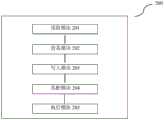
基于上述目的,本发明的实施例的第二个方面,提出了一种信号完整性优化的设备,如图2所示,设备200包括:Based on the above purpose, the second aspect of the embodiment of the present invention proposes a device for optimizing signal integrity. As shown in FIG. 2 , the
读取模块,读取模块配置为读取PCB网表和原理图以获取目标单板的所有网络信息;A reading module, the reading module is configured to read the PCB netlist and schematic diagram to obtain all network information of the target single board;
仿真模块,仿真模块配置为使用网络信息对目标单板进行仿真并获得优化目标单板的物理结构的仿真结果;a simulation module, the simulation module is configured to use network information to simulate the target single board and obtain a simulation result of optimizing the physical structure of the target single board;
写入模块,写入模块配置为基于仿真结果将相应的数据写入图形化模板中;A write module, the write module is configured to write corresponding data into the graphical template based on the simulation results;
匹配模块,匹配模块配置为将图形化模板中的数据与网络信息进行匹配;a matching module, the matching module is configured to match the data in the graphical template with the network information;
执行模块,执行模块配置为响应于图形化模板中的数据与网络信息匹配成功,对目标单板执行图形化模板中的数据的优化。An execution module, configured to execute optimization of the data in the graphical template on the target single board in response to the data in the graphical template successfully matching the network information.
在本发明的一个优选实施例中,网络信息包括网络名、网络两端的器件名称、器件类型、器件扇出孔的属性和换层信息。In a preferred embodiment of the present invention, the network information includes the name of the network, device names at both ends of the network, device types, attributes of device fan-out holes, and layer change information.
在本发明的一个优选实施例中,仿真模块还配置为:In a preferred embodiment of the present invention, simulation module is also configured as:
对单板的不同网络、不同器件类型和不同扇出焊盘类型进行仿真;Simulate different networks, different device types and different fan-out pad types of the single board;
调整可优化的参数进行仿真以优化焊盘的物理结构。Adjust the parameters that can be optimized for simulation to optimize the physical structure of the pad.
在本发明的一个优选实施例中,可优化的参数包括扇出过孔的孔径、扇出过孔的常规焊盘直径、扇出过孔的反焊盘直径、扇出信号平行布线长度、扇出信号拐角布线长度和差分信号P/N扇出间距。In a preferred embodiment of the present invention, the parameters that can be optimized include the diameter of the fan-out via, the diameter of the conventional pad of the fan-out via, the diameter of the anti-pad of the fan-out via, the length of the parallel wiring of the fan-out signal, the fan-out Outgoing signal corner routing length and differential signal P/N fanout spacing.
在本发明的一个优选实施例中,匹配模块还配置为:In a preferred embodiment of the present invention, the matching module is also configured as:
将图形化模板中的网络名与目标单板的网络名进行匹配;Match the network name in the graphical template with the network name of the target board;
响应于匹配成功,将相同网络名中两个网络的网络连接的器件管脚、管脚焊盘和布线进行匹配。In response to a successful match, the device pins, pin pads, and wires of the net connections of the two nets in the same net name are matched.
上述实施例,特别是任何“优选”实施例是实现的可能示例,并且仅为了清楚地理解本发明的原理而提出。可以在不脱离本文所描述的技术的精神和原理的情况下对上述实施例进行许多变化和修改。所有修改旨在被包括在本公开的范围内并且由所附权利要求保护。The above-described embodiments, particularly any "preferred" embodiments, are possible examples of implementations, and were merely presented for a clear understanding of the principles of the invention. Many changes and modifications can be made to the above-described embodiments without departing from the spirit and principles of the technology described herein. All modifications are intended to be included within the scope of this disclosure and protected by the appended claims.
Claims (8)
Priority Applications (1)
| Application Number | Priority Date | Filing Date | Title |
|---|---|---|---|
| CN202011354997.2ACN112446182B (en) | 2020-11-27 | 2020-11-27 | Method and equipment for optimizing signal integrity |
Applications Claiming Priority (1)
| Application Number | Priority Date | Filing Date | Title |
|---|---|---|---|
| CN202011354997.2ACN112446182B (en) | 2020-11-27 | 2020-11-27 | Method and equipment for optimizing signal integrity |
Publications (2)
| Publication Number | Publication Date |
|---|---|
| CN112446182A CN112446182A (en) | 2021-03-05 |
| CN112446182Btrue CN112446182B (en) | 2023-04-28 |
Family
ID=74738236
Family Applications (1)
| Application Number | Title | Priority Date | Filing Date |
|---|---|---|---|
| CN202011354997.2AActiveCN112446182B (en) | 2020-11-27 | 2020-11-27 | Method and equipment for optimizing signal integrity |
Country Status (1)
| Country | Link |
|---|---|
| CN (1) | CN112446182B (en) |
Families Citing this family (2)
| Publication number | Priority date | Publication date | Assignee | Title |
|---|---|---|---|---|
| CN113435157A (en)* | 2021-07-08 | 2021-09-24 | 苏州悦谱半导体有限公司 | Method for analyzing industrial graphic computer-aided manufacturing network data |
| CN118153506B (en)* | 2024-05-09 | 2024-08-16 | 上海合见工业软件集团有限公司 | Pad data exchange method, device, equipment and medium |
Citations (1)
| Publication number | Priority date | Publication date | Assignee | Title |
|---|---|---|---|---|
| CN108763717A (en)* | 2018-05-22 | 2018-11-06 | 郑州云海信息技术有限公司 | A kind of high speed link signal integrality fast evaluation method and system |
- 2020
- 2020-11-27CNCN202011354997.2Apatent/CN112446182B/enactiveActive
Patent Citations (1)
| Publication number | Priority date | Publication date | Assignee | Title |
|---|---|---|---|---|
| CN108763717A (en)* | 2018-05-22 | 2018-11-06 | 郑州云海信息技术有限公司 | A kind of high speed link signal integrality fast evaluation method and system |
Also Published As
| Publication number | Publication date |
|---|---|
| CN112446182A (en) | 2021-03-05 |
Similar Documents
| Publication | Publication Date | Title |
|---|---|---|
| US9361415B1 (en) | Method, system, and computer program product for implementing a multi-fabric electronic design spanning across multiple design fabrics | |
| CN113486625B (en) | Chip verification method and verification system | |
| CN109492310B (en) | Method and device for checking circuit | |
| CN111475355B (en) | High-speed link signal integrity evaluation method, system, terminal and storage medium | |
| TW202411872A (en) | Verification system, verification method, electronic device and storage medium | |
| US10860776B1 (en) | Printed circuit board (PCB) modular design | |
| US20080155483A1 (en) | Database-aided circuit design system and method therefor | |
| CN112446182B (en) | Method and equipment for optimizing signal integrity | |
| CN108763717A (en) | A kind of high speed link signal integrality fast evaluation method and system | |
| CN114117989A (en) | Chip design method, chip design device, computer equipment and storage medium | |
| CN115081389B (en) | A printed circuit board wiring inspection method, device, equipment and storage medium | |
| CN113466733A (en) | Power performance testing method and device, electronic equipment and storage medium | |
| CN113705143A (en) | Automatic simulation system and automatic simulation method | |
| CN100382085C (en) | Layout design method and device for integrated design components in printed circuit board | |
| John et al. | Ai workbench-conceptual workflow to develop ai models for si/pi-applications in pcb development | |
| CN114692537A (en) | FPGA circuit TILE level connection checking method and device, electronic equipment and storage medium | |
| US7984398B1 (en) | Automated multiple voltage/power state design process and chip description system | |
| CN118133742A (en) | Bit stream testing method, bit stream testing device, bit stream testing computer device, bit stream testing storage medium and bit stream testing program product | |
| US10783307B1 (en) | System and method for power-grid aware simulation of an IC-package schematic | |
| CN116629192A (en) | A high-speed link system topology generation method, system, device and medium | |
| CN113939091B (en) | Impedance matching design method and device of link electrostatic impedance device and printed circuit board | |
| CN116681030A (en) | Signing checking method, device, equipment and storage medium | |
| CN105792532B (en) | A kind of tear system of selection and PCB | |
| CN115438622A (en) | Evaluation system and evaluation method for product layout | |
| CN114423184B (en) | Special-shaped anti-bonding pad manufacturing method and device, electronic equipment and storage medium |
Legal Events
| Date | Code | Title | Description |
|---|---|---|---|
| PB01 | Publication | ||
| PB01 | Publication | ||
| SE01 | Entry into force of request for substantive examination | ||
| SE01 | Entry into force of request for substantive examination | ||
| GR01 | Patent grant | ||
| GR01 | Patent grant | ||
| CP03 | Change of name, title or address | Address after:Building 9, No.1, guanpu Road, Guoxiang street, Wuzhong Economic Development Zone, Wuzhong District, Suzhou City, Jiangsu Province Patentee after:Suzhou Yuannao Intelligent Technology Co.,Ltd. Country or region after:China Address before:Building 9, No.1, guanpu Road, Guoxiang street, Wuzhong Economic Development Zone, Wuzhong District, Suzhou City, Jiangsu Province Patentee before:SUZHOU LANGCHAO INTELLIGENT TECHNOLOGY Co.,Ltd. Country or region before:China |