CN112350751B - A multi-channel broadband amplitude and phase calibration device for satellite communication - Google Patents
A multi-channel broadband amplitude and phase calibration device for satellite communicationDownload PDFInfo
- Publication number
- CN112350751B CN112350751BCN202011213869.6ACN202011213869ACN112350751BCN 112350751 BCN112350751 BCN 112350751BCN 202011213869 ACN202011213869 ACN 202011213869ACN 112350751 BCN112350751 BCN 112350751B
- Authority
- CN
- China
- Prior art keywords
- amplitude
- module
- channel
- phase error
- signal
- Prior art date
- Legal status (The legal status is an assumption and is not a legal conclusion. Google has not performed a legal analysis and makes no representation as to the accuracy of the status listed.)
- Active
Links
Images

Classifications
- H—ELECTRICITY
- H04—ELECTRIC COMMUNICATION TECHNIQUE
- H04B—TRANSMISSION
- H04B17/00—Monitoring; Testing
- H04B17/10—Monitoring; Testing of transmitters
- H04B17/11—Monitoring; Testing of transmitters for calibration
- H—ELECTRICITY
- H04—ELECTRIC COMMUNICATION TECHNIQUE
- H04B—TRANSMISSION
- H04B17/00—Monitoring; Testing
- H04B17/20—Monitoring; Testing of receivers
- H04B17/21—Monitoring; Testing of receivers for calibration; for correcting measurements
- H—ELECTRICITY
- H04—ELECTRIC COMMUNICATION TECHNIQUE
- H04B—TRANSMISSION
- H04B7/00—Radio transmission systems, i.e. using radiation field
- H04B7/005—Control of transmission; Equalising
- H—ELECTRICITY
- H04—ELECTRIC COMMUNICATION TECHNIQUE
- H04B—TRANSMISSION
- H04B7/00—Radio transmission systems, i.e. using radiation field
- H04B7/14—Relay systems
- H04B7/15—Active relay systems
- H04B7/185—Space-based or airborne stations; Stations for satellite systems
- H04B7/1851—Systems using a satellite or space-based relay
- Y—GENERAL TAGGING OF NEW TECHNOLOGICAL DEVELOPMENTS; GENERAL TAGGING OF CROSS-SECTIONAL TECHNOLOGIES SPANNING OVER SEVERAL SECTIONS OF THE IPC; TECHNICAL SUBJECTS COVERED BY FORMER USPC CROSS-REFERENCE ART COLLECTIONS [XRACs] AND DIGESTS
- Y02—TECHNOLOGIES OR APPLICATIONS FOR MITIGATION OR ADAPTATION AGAINST CLIMATE CHANGE
- Y02D—CLIMATE CHANGE MITIGATION TECHNOLOGIES IN INFORMATION AND COMMUNICATION TECHNOLOGIES [ICT], I.E. INFORMATION AND COMMUNICATION TECHNOLOGIES AIMING AT THE REDUCTION OF THEIR OWN ENERGY USE
- Y02D30/00—Reducing energy consumption in communication networks
- Y02D30/70—Reducing energy consumption in communication networks in wireless communication networks
Landscapes
- Engineering & Computer Science (AREA)
- Computer Networks & Wireless Communication (AREA)
- Signal Processing (AREA)
- Physics & Mathematics (AREA)
- Electromagnetism (AREA)
- Astronomy & Astrophysics (AREA)
- Aviation & Aerospace Engineering (AREA)
- General Physics & Mathematics (AREA)
- Digital Transmission Methods That Use Modulated Carrier Waves (AREA)
Abstract
Translated fromChinese
Description
Translated fromChinese技术领域technical field
本发明属于数字相控阵天线的阵列信号处理与卫星通信的信号处理领域,具体涉及一种用于卫星通信的多通道宽频带幅相校准装置。The invention belongs to the field of digital phased array antenna array signal processing and satellite communication signal processing, in particular to a multi-channel broadband amplitude and phase calibration device for satellite communication.
背景技术Background technique
有源相控阵天线因为其体积小、损耗低、低轮廓、易于实现波束调零、波束赋形、多波束,同时可敏捷调整波束指向等优点,近年来应用广泛。但是由于器件的不一致性、环境变化等多种因素,相控阵天线可能会出现较大的幅相误差,导致增益降低、副瓣升高,所以需要具备接收和发射通道自校准功能。传统的收发通道校准方法一般采用收发单频信号的方式进行校准,每次只能校准单个频点的幅相误差。当相控阵天线工作在不同频率范围内时,为保证幅相校准的精度,需要重新进行校准且精度较低。另外,传统的发射通道校准需要外部连线进行辅助测试,将每一个发射通道连接到一个接收通道上,多路信号同时发射并环回以测试整个环路的幅相误差,最后根据整个环路的幅相误差和接收通道的幅相误差计算出发射通道的幅相误差信息,操作复杂。Active phased array antennas have been widely used in recent years because of their advantages of small size, low loss, low profile, easy to achieve beam nulling, beamforming, multi-beam, and agile adjustment of beam pointing. However, due to various factors such as device inconsistency and environmental changes, phased array antennas may have large amplitude and phase errors, resulting in reduced gain and increased side lobes. Therefore, it is necessary to have the function of self-calibration of the receiving and transmitting channels. The traditional transceiver channel calibration method generally adopts the method of transmitting and receiving single-frequency signals for calibration, and can only calibrate the amplitude and phase errors of a single frequency point each time. When the phased array antenna works in different frequency ranges, in order to ensure the accuracy of the amplitude and phase calibration, it needs to be re-calibrated and the accuracy is low. In addition, the traditional transmit channel calibration requires an external connection for auxiliary testing. Each transmit channel is connected to a receive channel, and multiple signals are simultaneously transmitted and looped back to test the amplitude and phase errors of the entire loop. Finally, according to the entire loop The amplitude and phase error of the receiving channel and the amplitude and phase error of the receiving channel are calculated to calculate the amplitude and phase error information of the transmitting channel, and the operation is complicated.
发明内容SUMMARY OF THE INVENTION
本发明的目的在于避免上述背景技术中的不足之处而提供一种用于卫星通信的多通道宽频带幅相校准装置,本发明采用数字信号处理技术实现通道间多个频点幅相误差检测、校正,具有测量精度高、集成化程度高、可靠性高、调试方便易于扩展等特点。The purpose of the present invention is to avoid the deficiencies in the above background technology and provide a multi-channel broadband amplitude and phase calibration device for satellite communication. The present invention adopts digital signal processing technology to realize the detection of amplitude and phase errors of multiple frequency points between channels , calibration, has the characteristics of high measurement accuracy, high integration, high reliability, convenient debugging and easy expansion.
为了实现上述目的,本发明采用的技术方案为:In order to achieve the above object, the technical scheme adopted in the present invention is:
一种用于卫星通信的多通道宽频带幅相校准装置,包括控制器、电源处理模块、多路选择器、均衡模块、幅相误差计算模块以及多个TR组件,幅相误差计算模块与均衡模块连接,每个TR组件均通过一条上变频通路和一条第一下变频通路与所述均衡模块连接,各第一下变频通路还与所述幅相误差计算模块连接;此外,各TR组件还与所述多路选择器连接,多路选择器通过第二下变频通路与所述幅相误差计算模块连接;各下变频通路均包括沿信号方向顺次连接的模数转换器和数字下变频器,各上变频通路均包括沿信号方向顺次连接的数字上变频器和数模转换器;A multi-channel broadband amplitude and phase calibration device for satellite communication, comprising a controller, a power supply processing module, a multiplexer, an equalization module, an amplitude and phase error calculation module and a plurality of TR components, the amplitude and phase error calculation module and the equalizer module connection, each TR component is connected with the equalization module through an up-conversion channel and a first down-conversion channel, and each first down-conversion channel is also connected with the amplitude-phase error calculation module; in addition, each TR component also connected with the multiplexer, and the multiplexer is connected with the amplitude-phase error calculation module through a second down-conversion path; each down-conversion path includes an analog-to-digital converter and a digital down-conversion connected in sequence along the signal direction Each up-conversion channel includes a digital up-converter and a digital-to-analog converter connected in sequence along the signal direction;
进行接收通道幅相误差校准时,TR组件接收外部输入的宽带校准信号并输出至相应第一下变频通路的模数转换器,进行模数变换后将数字信号输出到相应的数字下变频器;数字下变频器将接收的数字信号下变频到基带之后分两路进行传输:一路信号输出到幅相误差计算模块,在控制器的控制下计算出各个接收通道之间的幅相误差,并将幅相误差信息下发到均衡模块;另一路信号则直接输出到均衡模块,在均衡模块中根据幅相误差计算模块下发的幅相误差信息,对各个接收通道信号的幅度和相位误差进行校正;最后,均衡模块将已校正过幅相误差的各接收通道信号输出;When performing the amplitude and phase error calibration of the receiving channel, the TR component receives the externally input wideband calibration signal and outputs it to the analog-to-digital converter of the corresponding first down-conversion channel, and outputs the digital signal to the corresponding digital down-converter after analog-to-digital conversion; The digital down-converter down-converts the received digital signal to the baseband and transmits it in two ways: one signal is output to the amplitude and phase error calculation module, and the amplitude and phase errors between each receiving channel are calculated under the control of the controller, and the The amplitude and phase error information is sent to the equalization module; the other signal is directly output to the equalization module. In the equalization module, the amplitude and phase errors of each receiving channel signal are corrected according to the amplitude and phase error information sent by the amplitude and phase error calculation module. ;Finally, the equalization module outputs the signals of each receiving channel whose amplitude and phase errors have been corrected;
进行发射通道幅相误差校准时,首先由控制器控制均衡模块输出宽带信号给各数字上变频器,数字上变频器将上变频后的信号输出到相应的数模转换器,数模转换器将数模转换后的信号输出到相应的TR组件,TR组件通过发耦合通道将发射信号环回至多路选择器,多路选择器根据控制器下发的控制信号,选通其中一路耦合过来的信号输出到第二下变频通路中的模数转换器,完成模数转换后将信号输出到第二下变频通路中的数字下变频器,数字下变频之后再将信号输出到幅相误差计算模块,在控制器的控制下开始计算发射通道的幅相误差,并将幅相误差信息下发至均衡模块,根据下发的幅相误差信息在均衡模块中对发射信号进行幅相校正并输出。When performing the amplitude and phase error calibration of the transmitting channel, the controller controls the equalization module to output broadband signals to each digital up-converter, and the digital up-converter outputs the up-converted signal to the corresponding digital-to-analog converter. The digital-to-analog converted signal is output to the corresponding TR component, and the TR component loops the transmit signal back to the multiplexer through the transmit coupling channel, and the multiplexer selects one of the coupled signals according to the control signal sent by the controller. output to the analog-to-digital converter in the second down-conversion channel, output the signal to the digital down-converter in the second down-conversion channel after the analog-to-digital conversion is completed, and then output the signal to the amplitude-phase error calculation module after the digital down-conversion, Under the control of the controller, the amplitude and phase errors of the transmitting channel are calculated, and the amplitude and phase error information is sent to the equalization module, and the transmitted signal is corrected and output in the equalization module according to the sent amplitude and phase error information.
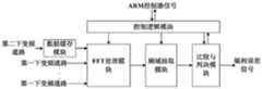
进一步的,所述幅相误差计算模块包括控制逻辑模块、数据缓存模块、FFT处理模块、频域抽取模块以及比较与判决模块;Further, the amplitude and phase error calculation module includes a control logic module, a data buffer module, an FFT processing module, a frequency domain extraction module, and a comparison and judgment module;
进行接收通道幅相误差校准时,各第一下变频通路的信号输出到FFT处理模块,FFT处理模块对各路校准信号进行快速傅立叶变换,得到各路信号的频谱并将频谱数据输出到频域抽取模块;所述控制器根据实际工作频段确定需要进行幅相误差测试的各个频点,然后将频点信息下发到控制逻辑模块,控制逻辑模块再将频点信息转发到频域抽取模块;频域抽取模块根据控制逻辑模块下发的频点信息,抽取各路接收信号频谱上相应频点的频谱数据,并将抽取的频谱数据输出到比较与判决模块;比较与判决模块根据抽取的频谱数据计算各通道中各频点的幅度和相位,根据计算出的幅度、相位信息计算各通道各频点的幅相误差,并对计算出的幅相误差信息进行判决,若判定无效则将这一信息经过控制逻辑模块上传到所述控制器,由所述控制器下发指令,重新启动接收通道的幅相误差计算流程,若判定有效则将信息下发到所述均衡模块用于接收信号的通道间幅相误差校正;When performing the amplitude and phase error calibration of the receiving channel, the signals of each first down-conversion channel are output to the FFT processing module, and the FFT processing module performs fast Fourier transform on the calibration signals of each channel to obtain the spectrum of each channel and output the spectrum data to the frequency domain. an extraction module; the controller determines each frequency point that needs to be tested for amplitude and phase error according to the actual working frequency band, and then sends the frequency point information to the control logic module, and the control logic module forwards the frequency point information to the frequency domain extraction module; The frequency domain extraction module extracts the spectrum data of the corresponding frequency points on the spectrum of each received signal according to the frequency point information issued by the control logic module, and outputs the extracted spectrum data to the comparison and judgment module; the comparison and judgment module is based on the extracted spectrum. The data calculates the amplitude and phase of each frequency point in each channel, calculates the amplitude and phase error of each frequency point of each channel according to the calculated amplitude and phase information, and judges the calculated amplitude and phase error information. A piece of information is uploaded to the controller through the control logic module, and the controller sends an instruction to restart the amplitude and phase error calculation process of the receiving channel. If it is determined to be valid, the information is sent to the equalization module for receiving signals. Amplitude and phase error correction between channels;
进行发射通道幅相误差校准时,所述均衡模块在内部生成用于校准的线性调频信号,并经各上变频通路输出给相应的TR组件,然后该信号又从TR组件的发耦合通道输出至所述多路选择器;所述控制器控制所述多路选择器依次选通各路发耦合通道,每次选通时该信号经第二下变频通路输出到数据缓存模块;待各路数据全部缓存完成后,将所有缓存数据输出到FFT处理模块进行快速傅立叶变换,此时,所述控制器根据实际工作频段,确定需要计算幅相误差的各个频点,并将频点信息经由控制逻辑模块下发到频域抽取模块,并据此在频域抽取模块中抽取各路发射信号频谱上相应频点的频谱数据,之后将这些频谱数据送至比较与判决模块;比较与判决模块根据抽取的频谱数据计算各通道各频点的幅度和相位,根据计算出的幅度、相位信息计算各通道各频点的幅相误差,并对计算出的幅相误差信息进行判决,若无效则将这一信息经过控制逻辑模块上传到所述控制器,由所述控制器下发指令,重新启动发射通道的幅相误差计算流程,若有效则将信息下发到所述均衡模块,用于发射信号的通道间幅相误差校准。When performing the amplitude and phase error calibration of the transmit channel, the equalization module internally generates a chirp signal for calibration, and outputs it to the corresponding TR component through each up-conversion channel, and then the signal is output from the transmit-coupling channel of the TR component to the TR component. the multiplexer; the controller controls the multiplexer to sequentially select each transmission coupling channel, and each time the signal is selected, the signal is output to the data buffer module through the second down-conversion channel; After all the buffering is completed, all the buffered data are output to the FFT processing module for fast Fourier transform. At this time, the controller determines each frequency point that needs to calculate the amplitude and phase error according to the actual working frequency band, and passes the frequency point information through the control logic. The module is sent to the frequency domain extraction module, and accordingly, the frequency domain extraction module extracts the spectral data of the corresponding frequency points on the spectrum of each transmission signal, and then sends these spectral data to the comparison and judgment module; the comparison and judgment module is based on the extraction Calculate the amplitude and phase of each frequency point of each channel, calculate the amplitude and phase error of each frequency point of each channel according to the calculated amplitude and phase information, and judge the calculated amplitude and phase error information. A piece of information is uploaded to the controller through the control logic module, and the controller sends an instruction to restart the amplitude and phase error calculation process of the transmitting channel. If it is valid, the information is sent to the equalization module for transmitting signals. The channel-to-channel amplitude and phase error calibration.
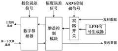
进一步的,所述均衡模块包括数字移相器、增益控制模块、双路开关以及线性调频信号生成器;Further, the equalization module includes a digital phase shifter, a gain control module, a two-way switch and a linear frequency modulation signal generator;
对于接收通道,各个通道的接收信号依次经过数字移相器和增益控制模块,根据所述幅相误差计算模块下发的幅相误差信息,完成各路接收通道的幅相误差校准;For the receiving channel, the received signals of each channel pass through the digital phase shifter and the gain control module in turn, and complete the amplitude and phase error calibration of each receiving channel according to the amplitude and phase error information sent by the amplitude and phase error calculation module;
对于发射通道,若当前处于校准模式,则由所述控制器控制双路开关将发射数据源切换到线性调频信号生成器,以发送宽带线性调频信号用于校准;若当前处于正常工作模式,则由所述控制器控制双路开关将发射数据源切换为实际需要发射的数据,各通道的发射数据依次经过增益控制模块和数字移相器,从而完成各路发射信号的幅相误差校准。For the transmit channel, if it is currently in the calibration mode, the controller controls the two-way switch to switch the transmit data source to the chirp signal generator, so as to send the broadband chirp signal for calibration; if it is currently in the normal working mode, then The controller controls the two-way switch to switch the transmission data source to the data that actually needs to be transmitted, and the transmission data of each channel passes through the gain control module and the digital phase shifter in turn, so as to complete the amplitude and phase error calibration of each transmission signal.
进一步的,该装置基于FPGA实现。Further, the device is implemented based on FPGA.
本发明与背景技术相比具有如下优点:Compared with the background technology, the present invention has the following advantages:
1.本发明采用数字信号处理技术实现多通道幅相误差检测及校准,对接收通道而言,首先接收外部宽带校准信号,对各通道信号进行频谱分析,根据实际工作频段确定需要检测相位误差的各个频点,同时对各个接收通道各频点的幅相误差信息进行检测;对发射通道而言,根据当前实际工作频段和信号带宽生成用于校准的线性调频信号,以对发射通道进行校准。相比于传统的用单音信号校准通道间幅相误差的方式,本发明大大降低了操作的复杂度,提高了校准的实时性和可靠性。1. The present invention adopts digital signal processing technology to realize multi-channel amplitude and phase error detection and calibration. For the receiving channel, the external broadband calibration signal is firstly received, and spectrum analysis is performed on the signal of each channel, and the phase error that needs to be detected is determined according to the actual working frequency band. For each frequency point, the amplitude and phase error information of each frequency point of each receiving channel is detected at the same time; for the transmitting channel, a chirp signal for calibration is generated according to the current actual working frequency band and signal bandwidth to calibrate the transmitting channel. Compared with the traditional method of calibrating the amplitude and phase errors between channels with a single tone signal, the present invention greatly reduces the complexity of the operation and improves the real-time performance and reliability of the calibration.
2.本发明在均衡模块中采用数字移相器代替了传统模拟相控阵所采用的模拟移相器,具有精度高、可靠性高、适应性强等特点。2. The present invention uses digital phase shifters in the equalization module to replace the analog phase shifters used in traditional analog phased arrays, and has the characteristics of high precision, high reliability, and strong adaptability.
3.本发明在处理发射通道校准时,各发射通道的宽带线性调频校准信号均通过基于多路选择器的同一条环回支路回传到均衡模块内部,大大降低了设备复杂度,无需每次进行发射通道校准时进行手动连线,极大提高了发射通道幅相误差校准的有效性与可用性。3. When the present invention processes the calibration of the transmission channel, the broadband chirp calibration signal of each transmission channel is returned to the inside of the equalization module through the same loop-back branch based on the multiplexer, which greatly reduces the complexity of the equipment and does not require every Manual connection is performed when the transmission channel calibration is performed for the second time, which greatly improves the effectiveness and usability of the amplitude and phase error calibration of the transmission channel.
附图说明Description of drawings
图1是本发明实施例的电原理方框图。FIG. 1 is a block diagram of an electrical principle of an embodiment of the present invention.
图2是本发明实施例中幅相误差计算模块的电原理方框图。FIG. 2 is a block diagram of an electrical principle of an amplitude-phase error calculation module in an embodiment of the present invention.
图3是本发明实施例中均衡模块的电原理方框图。FIG. 3 is a block diagram of an electrical principle of an equalization module in an embodiment of the present invention.
具体实施方式Detailed ways
下面结合附图和具体实施方式对本发明的技术方案做进一步的详细说明。The technical solutions of the present invention will be further described in detail below with reference to the accompanying drawings and specific embodiments.
参照图1~图3,一种用于卫星通信的多通道宽频带幅相校准装置,其包括ARM控制器、多路选择器、电源处理模块、均衡模块、幅相误差计算模块以及多个TR组件,幅相误差计算模块与均衡模块连接,每个TR组件均通过一条上变频通路和一条第一下变频通路与所述均衡模块连接,各第一下变频通路还与所述幅相误差计算模块连接;此外,各TR组件还与所述多路选择器连接,多路选择器通过第二下变频通路与所述幅相误差计算模块连接;各下变频通路均包括沿信号方向顺次连接的模数转换器和数字下变频器,各上变频通路均包括沿信号方向顺次连接的数字上变频器和数模转换器。图1是本实施例的电原理方框图,实施例按图1连接线路。1 to 3, a multi-channel broadband amplitude and phase calibration device for satellite communication, which includes an ARM controller, a multiplexer, a power processing module, an equalization module, an amplitude and phase error calculation module, and a plurality of TRs component, the amplitude and phase error calculation module is connected with the equalization module, each TR component is connected with the equalization module through an up-conversion path and a first down-conversion path, and each first down-conversion path is also connected with the amplitude-phase error calculation module connection; in addition, each TR component is also connected with the multiplexer, and the multiplexer is connected with the amplitude-phase error calculation module through the second down-conversion path; each down-conversion path includes sequential connections along the signal direction Each of the up-conversion paths includes a digital up-converter and a digital-to-analog converter connected in sequence along the signal direction. FIG. 1 is a block diagram of the electrical principle of this embodiment, and the embodiment is connected according to FIG. 1 .
其中,TR组件的作用是收发电磁波信号,且包含一个发耦合通道,发射通道信号会从该通道耦合出来以供调试、校准用。本例中所采用的模数转换器均为市售AD9361,所采用的所有数模转换器均为市售AD9364。本例还采用了市售XC7Z045型号的FPGA芯片实现,其封装为ffg900,所有数字上变频、数字下变频模块均由FPGA芯片中的DUC/DDC Compiler制作,单个DUC/DDC Compiler最多同时支持8通道信号的数字上/下变频;ARM控制器由FPGA芯片内嵌的双核Cortex-A9芯片制作,其作用是对整个收发通道的校准流程进行控制和监督。幅相误差计算模块、均衡模块均在FPGA内部实现,电源处理模块采用市售开关电源调整器PTH05000、线性稳压器LT1764EQ-1.8、LT1764EQ-3.3制作,其作用是提供各级部件直流工作电压。Among them, the function of the TR component is to send and receive electromagnetic wave signals, and includes a transmission coupling channel, and the transmission channel signal will be coupled out from this channel for debugging and calibration. The analog-to-digital converters used in this example are the commercially available AD9361, and all the digital-to-analog converters used are the commercially available AD9364. This example is also implemented with a commercially available FPGA chip of XC7Z045, which is packaged as ffg900. All digital up-conversion and digital down-conversion modules are made by the DUC/DDC Compiler in the FPGA chip. A single DUC/DDC Compiler supports up to 8 channels at the same time. The digital up/down conversion of the signal; the ARM controller is made of the dual-core Cortex-A9 chip embedded in the FPGA chip, and its function is to control and supervise the calibration process of the entire transceiver channel. The amplitude and phase error calculation module and the equalization module are all implemented inside the FPGA. The power processing module is made of the commercially available switching power supply regulator PTH05000, linear voltage regulators LT1764EQ-1.8 and LT1764EQ-3.3. Its function is to provide DC working voltages for all levels of components.
幅相误差计算模块主要作用包括:计算16个接收通道的幅相误差信息、计算16个发射通道的幅相误差信息、对计算结果进行判决。它包括控制逻辑模块、数据缓存模块、FFT处理模块、频域抽取模块、比较与判决模块。图2是幅相误差计算模块的电原理方框图,实施例按图2中的关系进行连接。控制逻辑模块由FPGA内部的可配置逻辑单元CLB制作,其作用是与ARM控制器进行数据交互,相当于是一个数据中转站。数据缓存模块由FPGA芯片内部的FIFO Generator制作,其作用是对从发耦合通道接收到的线性调频校准信号进行缓存。FFT处理模块由FPGA内部的LTE Fast Fourier Transform制作,其作用是将宽带信号变换到频域用于后续的幅相误差计算。频域抽取模块基于FPGA内部的可配置逻辑单元CLB制作,其作用是根据ARM控制器下发的频点信息,抽取各通道各频点的频谱数据。比较与判决模块由FPGA内部的可配置逻辑单元CLB制作,其作用是根据抽取的频谱数据计算各收发通道的幅相误差,并对通道间幅相误差的计算结果进行判决,若判定结果有误,则将异常信息经由控制逻辑模块上报给ARM控制器,重新启动幅相误差校准流程,若判定计算结果正确,则将幅相误差信息下发给均衡模块。The main functions of the amplitude and phase error calculation module include: calculating the amplitude and phase error information of the 16 receiving channels, calculating the amplitude and phase error information of the 16 transmitting channels, and making judgments on the calculation results. It includes control logic module, data buffer module, FFT processing module, frequency domain extraction module, comparison and judgment module. FIG. 2 is a block diagram of the electrical principle of the amplitude and phase error calculation module, and the embodiment is connected according to the relationship in FIG. 2 . The control logic module is made by the configurable logic unit CLB inside the FPGA, and its function is to exchange data with the ARM controller, which is equivalent to a data transfer station. The data buffer module is made by the FIFO Generator inside the FPGA chip, and its function is to buffer the linear frequency modulation calibration signal received from the transmitter coupling channel. The FFT processing module is made by the LTE Fast Fourier Transform inside the FPGA, and its function is to transform the broadband signal into the frequency domain for subsequent amplitude and phase error calculation. The frequency domain extraction module is based on the configurable logic unit CLB inside the FPGA. Its function is to extract the spectrum data of each frequency point of each channel according to the frequency point information sent by the ARM controller. The comparison and judgment module is made by the configurable logic unit CLB inside the FPGA. Its function is to calculate the amplitude and phase errors of each transceiver channel according to the extracted spectrum data, and to judge the calculation results of the amplitude and phase errors between the channels. If the judgment result is wrong , the abnormal information is reported to the ARM controller via the control logic module, and the amplitude and phase error calibration process is restarted. If it is determined that the calculation result is correct, the amplitude and phase error information is sent to the equalization module.
均衡模块主要作用包括对16路接收通道信号进行幅相误差校准、对16路发射通道信号进行幅相误差校准、生成线性调频宽带校准信号。它包括数字移相器、增益控制模块、双路开关、线性调频信号生成器。图3是均衡模块的电原理方框图,实施例按图3中的关系进行连接。线性调频信号生成器由FPGA内部的可配置逻辑单元结合DSP48E制作,可根据实际工作带宽设置线性调频信号的带宽和调频斜率。双路开关由FPGA内部可配置逻辑单元CLB制作,若当前为校准模式,则在ARM控制器下将数据源切换为线性调频信号生成器,若当前为正常工作模式,则将数据源切换为需要发射的信号。增益控制模块由FPGA内部的可配置逻辑单元CLB和DSP48E制作,增益控制模块默认增益为1,相当于直通模式,实际工作时,根据当前工作带宽的中心频率以及幅相误差计算模块下发的各通道间幅度误差信息,来确定当前各个收发通道的信号增益。数字移相器模块由FPGA内部CORDIC IP核制作,数字移相器默认移相值为0,相当于直通模式,实际工作时,根据当前工作带宽的中心频率以及幅相误差计算模块下发的各通道间相位误差信息,来确定当前各个收发通道的移相值,从而实现各通道间的相位校准。The main functions of the equalization module include the amplitude and phase error calibration of the 16-channel receiving channel signals, the amplitude and phase error calibration of the 16-channel transmitting channel signals, and the generation of linear frequency modulation wideband calibration signals. It includes a digital phase shifter, a gain control module, a two-way switch, and a chirp generator. FIG. 3 is a block diagram of the electrical principle of the equalization module, and the embodiment is connected according to the relationship in FIG. 3 . The linear frequency modulation signal generator is made by the configurable logic unit inside the FPGA combined with the DSP48E, which can set the bandwidth and frequency modulation slope of the linear frequency modulation signal according to the actual working bandwidth. The two-way switch is made by the configurable logic unit CLB inside the FPGA. If the current calibration mode is used, the data source will be switched to the linear frequency modulation signal generator under the ARM controller. If the current working mode is normal, the data source will be switched to the required transmitted signal. The gain control module is made by the configurable logic unit CLB and DSP48E inside the FPGA. The default gain of the gain control module is 1, which is equivalent to the straight-through mode. Inter-channel amplitude error information to determine the current signal gain of each transceiver channel. The digital phase shifter module is made by the internal CORDIC IP core of the FPGA. The default phase shift value of the digital phase shifter is 0, which is equivalent to the straight-through mode. The phase error information between the channels is used to determine the current phase shift value of each transceiver channel, so as to realize the phase calibration between the channels.
本装置的简要工作原理如下:The brief working principle of this device is as follows:
设线性调频信号生成器输出的信号为U1(t):Let the signal output by the chirp generator be U1 (t):

其中U1为信号幅度,k为调频斜率,T为脉冲宽度,f0为起始频率,信号带宽B=kT,rect(t/T)为矩形信号:Where U1 is the signal amplitude, k is the frequency modulation slope, T is the pulse width, f0 is the starting frequency, the signal bandwidth B=kT, and rect(t/T) is a rectangular signal:

线性调频信号U1(t)从均衡模块11输出,经过数字上变频和模数转换后,输出到16路TR组件的发射通道,之后在ARM控制器的控制下,依次选通各TR组件发耦合通道与多路选择器之间的数据通道,在经过模数转换器、数字下变频,将16路发射通道校准信号依次输出至数据缓存模块,数据缓存模块中的16路信号为:The linear frequency modulation signal U1 (t) is output from the equalization module 11. After digital up-conversion and analog-to-digital conversion, it is output to the transmitting channels of the 16 TR components. Then, under the control of the ARM controller, each TR component is sequentially selected to transmit The data channel between the coupling channel and the multiplexer, after going through the analog-to-digital converter and digital down-conversion, outputs the calibration signals of the 16 channels of transmission channels to the data buffer module in turn. The 16 channels of signals in the data buffer module are:

其中Ai为第i路接收通道信号的幅度,τi为第i路接收通道的时延,k为调频斜率,T为脉冲宽度,f0为起始频率。Among them, Ai is the amplitude of the signal of the i-th receiving channel, τi is the time delay of the i-th receiving channel, k is the frequency modulation slope, T is the pulse width, and f0 is the starting frequency.
数据缓存模块中16路线性调频信号依次经过FFT频谱处理模块、频域抽取模块,得到16通道各频点的频谱数据:The 16 linear FM signals in the data buffer module pass through the FFT spectrum processing module and the frequency domain extraction module in turn to obtain the spectrum data of each frequency point of the 16 channels:

其中,Fw(i,n)为第i路信号,第n个频点的频谱数据。Among them, Fw(i,n) is the frequency spectrum data of the i-th signal and the n-th frequency point.
频域抽取模块将抽取后的频谱数据输出到比较与判决模块,其他15路信号均以第1路信号为参考,计算其和第一路信号的幅相误差,得到相应的幅相误差数据:The frequency domain extraction module outputs the extracted spectrum data to the comparison and judgment module. The other 15 signals are all based on the first signal, and the amplitude and phase errors between them and the first signal are calculated to obtain the corresponding amplitude and phase error data:

其中,E(k,n)为第k路信号,在第n个频点上与第一路信号的幅相误差,E(k,n)为复数,模值表示幅度误差,相位表示相位误差。Among them, E(k,n) is the kth signal, the amplitude and phase error with the first signal at the nth frequency point, E(k,n) is a complex number, the modulus value represents the amplitude error, and the phase represents the phase error .
幅相误差计算模块将计算好的幅相误差信息下发到均衡模块。在均衡模块中,由ARM控制器控制双路开关将数据源切换到发射数据,设第i路实际发射信号为X1i(t),增益控制模块的输出信号X2i(t)为:The amplitude and phase error calculation module sends the calculated amplitude and phase error information to the equalization module. In the equalization module, the ARM controller controls the two-way switch to switch the data source to the transmission data. Let the actual transmission signal of the i-th channel be X1i (t), and the output signal X2i (t) of the gain control module is:
X2i(t)=X1i(t)×|E(i,n)| (6)X2i (t)=X1i (t)×|E(i,n)| (6)
其中E(i,n)为第i路信号与第1路信号在第n个频点的幅相误差,n值由发射通道实际工作带宽确定。Among them, E(i,n) is the amplitude and phase error between the ith signal and the first signal at the nth frequency, and the value of n is determined by the actual working bandwidth of the transmitting channel.
增益控制模块的输出信号X2i(t)经过数字移相器,得到相位校准后的信号X3i(t):The output signal X2i (t) of the gain control module passes through the digital phase shifter to obtain the phase calibrated signal X3i (t):
X3i(t)=X2i(t)×ej(angle(E(i,n))) (7)X3i (t)=X2i (t)×ej(angle(E(i,n))) (7)
其中E(i,n)为第i路信号与第1路信号在第n个频点的幅相误差,n值由发射通道实际工作带宽确定。Among them, E(i,n) is the amplitude and phase error between the ith signal and the first signal at the nth frequency, and the value of n is determined by the actual working bandwidth of the transmitting channel.
完成幅相误差校准的第i路发射信号X3i(t)经过数字上变频以及数模转换以后最终输出到TR组件并发射。接收通道校准流程与发射通道的校准流程的区别在于,接收通道校准时直接由TR组件接收用于校准的线性调频信号,其他工作流程完全一致。The i-th transmit signal X3i (t) that has completed the amplitude and phase error calibration is finally output to the TR component and transmitted after digital up-conversion and digital-to-analog conversion. The difference between the calibration process of the receiving channel and the calibration process of the transmitting channel is that the TR component directly receives the chirp signal for calibration during the calibration of the receiving channel, and the other workflows are exactly the same.
本装置的安装结构如下:全部电路元器件双面贴装在一块长×宽为200×180毫米的12层印制板上,顶层和底层为信号层,安装元器件,中间层为六层内电层和四层信号层,六层内电层包括四层数字地、模拟地分离的大面积接地层和两层隔离的电源层。为了避免通道间信号通过电源串扰,特别是AD9361捷变频器,每个芯片供电电源分别设置。实施例采用上、下层屏蔽盒体安装,除在射频信号区域分腔隔离设计外,在上层热量大的FPGA、电源芯片上,结合预埋热管和散热翅片的结构设计,形成良好的传导散热;该结构既可实现电磁信号的空间隔离,方便射频信号的就近接地端,避免了射频信号在盒体内部的相互干扰,又可高效的把芯片局部热量传导到整个盒体,通过密集的翅片向外散热。The installation structure of the device is as follows: all circuit components are mounted on both sides on a 12-layer printed board with a length x width of 200 x 180 mm, the top layer and the bottom layer are signal layers, components are installed, and the middle layer is six layers The electrical layer and the four-layer signal layer, and the six-layer inner electrical layer include four layers of digital ground, a large-area ground layer separated by analog ground, and two layers of isolated power supply layer. In order to avoid the crosstalk of signals between channels through the power supply, especially the AD9361 inverter, the power supply of each chip is set separately. The embodiment adopts the upper and lower shielding boxes for installation. In addition to the cavity isolation design in the RF signal area, on the FPGA and power chips with high heat in the upper layer, combined with the structural design of embedded heat pipes and heat dissipation fins, good conduction and heat dissipation are formed. ; This structure can not only realize the spatial isolation of electromagnetic signals, facilitate the nearby grounding end of radio frequency signals, avoid the mutual interference of radio frequency signals inside the box, but also efficiently conduct local heat of the chip to the entire box, through dense fins The chip dissipates heat outward.
本发明可以在整个工作频带内,实现多个数字通道之间幅相误差的高精度校准,从而为多通道数字波束控制及阵列信号处理奠定基础。该装置可实现接收通道和发射通道的幅相误差校准功能。其中,接收通道校准是通过TR组件、模数转换器、数字下变频模块把16路校准信号送到幅相误差计算模块,在ARM控制下进行各接收通道的幅相误差计算,并将计算好的幅相误差下发到均衡模块对接收信号的幅相误差进行校准;发射通道校准流程则是由TR组件发耦合通道经过多路选择器、模数转换器、数字下变频把校准信号输出到幅相误差计算模块。与接收通道不同的是,发射通道每次只能由ARM控制多路选择器传输一路校准信号到幅相误差计算模块并缓存,等接收完全部16通道校准信号后开始计算通道间幅相误差,并将计算结果下发至均衡模块。本发明采用基于宽带线性调频(LFM)信号的校准算法,相比于普遍应用的单音信号校准,可在数字域方便实现宽频带、多通道幅相误差校准功能,具有集成化程度高、结构简单、可靠性高、方便规模扩展等特点。The invention can realize the high-precision calibration of the amplitude and phase errors between multiple digital channels in the whole working frequency band, thereby laying a foundation for multi-channel digital beam control and array signal processing. The device can realize the amplitude and phase error calibration function of the receiving channel and the transmitting channel. Among them, the receiving channel calibration is to send 16 channels of calibration signals to the amplitude and phase error calculation module through the TR component, the analog-to-digital converter and the digital down-conversion module. Under the control of the ARM, the amplitude and phase errors of each receiving channel are calculated, and the calculated The amplitude and phase error of the received signal is sent to the equalization module to calibrate the amplitude and phase error of the received signal; the transmission channel calibration process is that the TR component sends the coupling channel through the multiplexer, analog-to-digital converter, and digital down-conversion to output the calibration signal to the Amplitude and phase error calculation module. Different from the receiving channel, the transmitting channel can only transmit one calibration signal by the ARM control multiplexer to the amplitude and phase error calculation module and buffer it. After receiving all the 16-channel calibration signals, the amplitude and phase errors between the channels are calculated. And send the calculation results to the equalization module. The present invention adopts the calibration algorithm based on wideband linear frequency modulation (LFM) signal, compared with the commonly used single tone signal calibration, it can conveniently realize the wideband and multi-channel amplitude and phase error calibration function in the digital domain, and has the advantages of high integration degree and structure. Simple, high reliability, convenient for scale expansion and so on.
Claims (3)
Priority Applications (1)
| Application Number | Priority Date | Filing Date | Title |
|---|---|---|---|
| CN202011213869.6ACN112350751B (en) | 2020-11-04 | 2020-11-04 | A multi-channel broadband amplitude and phase calibration device for satellite communication |
Applications Claiming Priority (1)
| Application Number | Priority Date | Filing Date | Title |
|---|---|---|---|
| CN202011213869.6ACN112350751B (en) | 2020-11-04 | 2020-11-04 | A multi-channel broadband amplitude and phase calibration device for satellite communication |
Publications (2)
| Publication Number | Publication Date |
|---|---|
| CN112350751A CN112350751A (en) | 2021-02-09 |
| CN112350751Btrue CN112350751B (en) | 2022-07-08 |
Family
ID=74356417
Family Applications (1)
| Application Number | Title | Priority Date | Filing Date |
|---|---|---|---|
| CN202011213869.6AActiveCN112350751B (en) | 2020-11-04 | 2020-11-04 | A multi-channel broadband amplitude and phase calibration device for satellite communication |
Country Status (1)
| Country | Link |
|---|---|
| CN (1) | CN112350751B (en) |
Families Citing this family (5)
| Publication number | Priority date | Publication date | Assignee | Title |
|---|---|---|---|---|
| CN113824491B (en)* | 2021-11-22 | 2022-01-21 | 中国人民解放军海军工程大学 | Ku/Ka dual-band satellite-communication ground station-oriented multi-frequency-point interference sampling circuit and method |
| CN115483988A (en)* | 2022-08-28 | 2022-12-16 | 复旦大学 | Multichannel phased array transmitter amplitude-phase calibration system and method |
| CN115575910A (en)* | 2022-08-31 | 2023-01-06 | 上海机电工程研究所 | Calibration system, device and calibration method of broadband target array |
| CN115987416A (en)* | 2022-12-14 | 2023-04-18 | 东南大学 | Hardware real-time online calibration method for radio frequency channel of wireless channel simulation architecture |
| CN116743170B (en)* | 2023-08-16 | 2023-10-13 | 南京芯惠半导体有限公司 | Multichannel analog-to-digital converter and calibration method thereof |
Citations (15)
| Publication number | Priority date | Publication date | Assignee | Title |
|---|---|---|---|---|
| CN101349741A (en)* | 2008-08-29 | 2009-01-21 | 西安电子科技大学 | Phased Array Digital Multi-beamformer for Electronic Reconnaissance |
| CN101957444A (en)* | 2010-09-30 | 2011-01-26 | 中国船舶重工集团公司第七二三研究所 | Multichannel radar amplitude and phase automatic correcting method and device |
| CN101964449A (en)* | 2010-08-27 | 2011-02-02 | 中国科学院上海微系统与信息技术研究所 | On-track correcting device of space-borne phased array transmitting antenna |
| CN103117781A (en)* | 2013-02-01 | 2013-05-22 | 华中科技大学 | Method and device for antenna array calibration under complex electromagnetic environment |
| CN103391123A (en)* | 2013-07-25 | 2013-11-13 | 中国科学院上海微系统与信息技术研究所 | Satellite-borne multi-beam receiving antenna correction system and method |
| CN104297738A (en)* | 2014-11-13 | 2015-01-21 | 中国科学院电子学研究所 | Synchronization calibration device and synchronization calibration and error compensation method for multi-channel receiver |
| CN104316913A (en)* | 2014-11-13 | 2015-01-28 | 中国科学院电子学研究所 | Multichannel receiver real-time calibration device and calibration and error compensation method |
| CN107315183A (en)* | 2017-06-01 | 2017-11-03 | 西南电子技术研究所(中国电子科技集团公司第十研究所) | The calibration method of aeronautical satellite array antenna received system |
| CN110149157A (en)* | 2018-02-11 | 2019-08-20 | 西南电子技术研究所(中国电子科技集团公司第十研究所) | Array antenna wideband channel parallel calibration method |
| CN110531325A (en)* | 2019-07-30 | 2019-12-03 | 中国人民解放军91550部队 | Digital if receiver and method for monopulse radar |
| CN209897046U (en)* | 2019-06-21 | 2020-01-03 | 成都九洲迪飞科技有限责任公司 | Small phased array digital radio frequency subsystem |
| CN110808794A (en)* | 2019-11-05 | 2020-02-18 | 中国电子科技集团公司第二十研究所 | Large-scale phased array calibration system based on dual-channel calibration circuit and control method |
| CN111245529A (en)* | 2020-04-09 | 2020-06-05 | 成都坤恒顺维科技股份有限公司 | Phase calibration method of digital phased array antenna and phased array antenna |
| CN111638494A (en)* | 2020-05-31 | 2020-09-08 | 西南电子技术研究所(中国电子科技集团公司第十研究所) | Multi-channel amplitude and phase correction method for digital beam synthesis system |
| CN111726173A (en)* | 2020-06-29 | 2020-09-29 | 中国电子科技集团公司第五十四研究所 | An internal calibration system and method for transmitting and receiving duplex phased array antennas |
- 2020
- 2020-11-04CNCN202011213869.6Apatent/CN112350751B/enactiveActive
Patent Citations (15)
| Publication number | Priority date | Publication date | Assignee | Title |
|---|---|---|---|---|
| CN101349741A (en)* | 2008-08-29 | 2009-01-21 | 西安电子科技大学 | Phased Array Digital Multi-beamformer for Electronic Reconnaissance |
| CN101964449A (en)* | 2010-08-27 | 2011-02-02 | 中国科学院上海微系统与信息技术研究所 | On-track correcting device of space-borne phased array transmitting antenna |
| CN101957444A (en)* | 2010-09-30 | 2011-01-26 | 中国船舶重工集团公司第七二三研究所 | Multichannel radar amplitude and phase automatic correcting method and device |
| CN103117781A (en)* | 2013-02-01 | 2013-05-22 | 华中科技大学 | Method and device for antenna array calibration under complex electromagnetic environment |
| CN103391123A (en)* | 2013-07-25 | 2013-11-13 | 中国科学院上海微系统与信息技术研究所 | Satellite-borne multi-beam receiving antenna correction system and method |
| CN104316913A (en)* | 2014-11-13 | 2015-01-28 | 中国科学院电子学研究所 | Multichannel receiver real-time calibration device and calibration and error compensation method |
| CN104297738A (en)* | 2014-11-13 | 2015-01-21 | 中国科学院电子学研究所 | Synchronization calibration device and synchronization calibration and error compensation method for multi-channel receiver |
| CN107315183A (en)* | 2017-06-01 | 2017-11-03 | 西南电子技术研究所(中国电子科技集团公司第十研究所) | The calibration method of aeronautical satellite array antenna received system |
| CN110149157A (en)* | 2018-02-11 | 2019-08-20 | 西南电子技术研究所(中国电子科技集团公司第十研究所) | Array antenna wideband channel parallel calibration method |
| CN209897046U (en)* | 2019-06-21 | 2020-01-03 | 成都九洲迪飞科技有限责任公司 | Small phased array digital radio frequency subsystem |
| CN110531325A (en)* | 2019-07-30 | 2019-12-03 | 中国人民解放军91550部队 | Digital if receiver and method for monopulse radar |
| CN110808794A (en)* | 2019-11-05 | 2020-02-18 | 中国电子科技集团公司第二十研究所 | Large-scale phased array calibration system based on dual-channel calibration circuit and control method |
| CN111245529A (en)* | 2020-04-09 | 2020-06-05 | 成都坤恒顺维科技股份有限公司 | Phase calibration method of digital phased array antenna and phased array antenna |
| CN111638494A (en)* | 2020-05-31 | 2020-09-08 | 西南电子技术研究所(中国电子科技集团公司第十研究所) | Multi-channel amplitude and phase correction method for digital beam synthesis system |
| CN111726173A (en)* | 2020-06-29 | 2020-09-29 | 中国电子科技集团公司第五十四研究所 | An internal calibration system and method for transmitting and receiving duplex phased array antennas |
Also Published As
| Publication number | Publication date |
|---|---|
| CN112350751A (en) | 2021-02-09 |
Similar Documents
| Publication | Publication Date | Title |
|---|---|---|
| CN112350751B (en) | A multi-channel broadband amplitude and phase calibration device for satellite communication | |
| US11522501B2 (en) | Phased array amplifier linearization | |
| CN103391123B (en) | Satellite-borne multi-beam receiving antenna correction system and correction method thereof | |
| CN113014294B (en) | Two-dimensional phased array microwave front end calibration network and method | |
| CN108562880B (en) | Internal calibration network unit and internal calibration method of reflector spaceborne SAR system | |
| CN114185008A (en) | Amplitude and phase error compensation system and method for receiving channel of narrowband digital array radar system | |
| CN102394679A (en) | System and method for calibrating transmission channel of satellite borne multi-beam antenna system in real time | |
| CN102426300A (en) | Satellite-borne beam forming receiving channel amplitude and phase error calibration system and method thereof | |
| CN105467371A (en) | Amplitude phase calibrating device for semi-closed loop coupled phased array channels | |
| CN103873166A (en) | Antenna system calibration | |
| CN114185017B (en) | Amplitude and phase error control method for active feed of azimuth multi-channel antenna | |
| US7088173B1 (en) | Adjustable multiport power/phase method and system with minimum phase error | |
| CN114185016B (en) | Measurement and Compensation Method for Inter-channel Amplitude and Phase Errors of Multi-channel Spaceborne SAR Antennas | |
| CN106842158A (en) | A kind of phased-array radar transmission channel phase alignment method of testing | |
| CN112698113B (en) | Amplitude calibration method and device for receiving channel and network equipment | |
| CN109683146A (en) | A kind of phased array emission calibrating method based on orthogonal coding waveform | |
| CN113573349A (en) | Performance test system and method of millimeter wave communication equipment | |
| CN107276643A (en) | A kind of moving communication satellite multi-beam carrier/interface ratio ground testing system and method | |
| CN111865448B (en) | Phased array antenna testing method and computer readable storage medium | |
| CN115390022A (en) | High-precision real-time dynamic test method for radar antenna internal calibration network | |
| CN111953430A (en) | Phased array antenna system level test system and test method | |
| CN105897351A (en) | Uplink and downlink wave beam shaping measure system and method | |
| CN112615680B (en) | Phase calibration method and device of transmitting channel and network equipment | |
| CN109921865B (en) | A system and method for approximating analog calibration of standard poles for all-space phased array antennas | |
| CN112615681B (en) | Amplitude calibration method and device of transmitting channel and network equipment |
Legal Events
| Date | Code | Title | Description |
|---|---|---|---|
| PB01 | Publication | ||
| PB01 | Publication | ||
| SE01 | Entry into force of request for substantive examination | ||
| SE01 | Entry into force of request for substantive examination | ||
| GR01 | Patent grant | ||
| GR01 | Patent grant |