CN112259041B - Pixel circuit and driving method thereof, and display device - Google Patents
Pixel circuit and driving method thereof, and display deviceDownload PDFInfo
- Publication number
- CN112259041B CN112259041BCN201910599791.7ACN201910599791ACN112259041BCN 112259041 BCN112259041 BCN 112259041BCN 201910599791 ACN201910599791 ACN 201910599791ACN 112259041 BCN112259041 BCN 112259041B
- Authority
- CN
- China
- Prior art keywords
- control
- transistor
- circuit
- driving
- light
- Prior art date
- Legal status (The legal status is an assumption and is not a legal conclusion. Google has not performed a legal analysis and makes no representation as to the accuracy of the status listed.)
- Active
Links
Images


Classifications
- G—PHYSICS
- G09—EDUCATION; CRYPTOGRAPHY; DISPLAY; ADVERTISING; SEALS
- G09G—ARRANGEMENTS OR CIRCUITS FOR CONTROL OF INDICATING DEVICES USING STATIC MEANS TO PRESENT VARIABLE INFORMATION
- G09G3/00—Control arrangements or circuits, of interest only in connection with visual indicators other than cathode-ray tubes
- G09G3/20—Control arrangements or circuits, of interest only in connection with visual indicators other than cathode-ray tubes for presentation of an assembly of a number of characters, e.g. a page, by composing the assembly by combination of individual elements arranged in a matrix no fixed position being assigned to or needed to be assigned to the individual characters or partial characters
- G09G3/22—Control arrangements or circuits, of interest only in connection with visual indicators other than cathode-ray tubes for presentation of an assembly of a number of characters, e.g. a page, by composing the assembly by combination of individual elements arranged in a matrix no fixed position being assigned to or needed to be assigned to the individual characters or partial characters using controlled light sources
- G09G3/30—Control arrangements or circuits, of interest only in connection with visual indicators other than cathode-ray tubes for presentation of an assembly of a number of characters, e.g. a page, by composing the assembly by combination of individual elements arranged in a matrix no fixed position being assigned to or needed to be assigned to the individual characters or partial characters using controlled light sources using electroluminescent panels
- G09G3/32—Control arrangements or circuits, of interest only in connection with visual indicators other than cathode-ray tubes for presentation of an assembly of a number of characters, e.g. a page, by composing the assembly by combination of individual elements arranged in a matrix no fixed position being assigned to or needed to be assigned to the individual characters or partial characters using controlled light sources using electroluminescent panels semiconductive, e.g. using light-emitting diodes [LED]
- G09G3/3208—Control arrangements or circuits, of interest only in connection with visual indicators other than cathode-ray tubes for presentation of an assembly of a number of characters, e.g. a page, by composing the assembly by combination of individual elements arranged in a matrix no fixed position being assigned to or needed to be assigned to the individual characters or partial characters using controlled light sources using electroluminescent panels semiconductive, e.g. using light-emitting diodes [LED] organic, e.g. using organic light-emitting diodes [OLED]
- G09G3/3225—Control arrangements or circuits, of interest only in connection with visual indicators other than cathode-ray tubes for presentation of an assembly of a number of characters, e.g. a page, by composing the assembly by combination of individual elements arranged in a matrix no fixed position being assigned to or needed to be assigned to the individual characters or partial characters using controlled light sources using electroluminescent panels semiconductive, e.g. using light-emitting diodes [LED] organic, e.g. using organic light-emitting diodes [OLED] using an active matrix
- G09G3/3233—Control arrangements or circuits, of interest only in connection with visual indicators other than cathode-ray tubes for presentation of an assembly of a number of characters, e.g. a page, by composing the assembly by combination of individual elements arranged in a matrix no fixed position being assigned to or needed to be assigned to the individual characters or partial characters using controlled light sources using electroluminescent panels semiconductive, e.g. using light-emitting diodes [LED] organic, e.g. using organic light-emitting diodes [OLED] using an active matrix with pixel circuitry controlling the current through the light-emitting element
- G—PHYSICS
- G09—EDUCATION; CRYPTOGRAPHY; DISPLAY; ADVERTISING; SEALS
- G09G—ARRANGEMENTS OR CIRCUITS FOR CONTROL OF INDICATING DEVICES USING STATIC MEANS TO PRESENT VARIABLE INFORMATION
- G09G2300/00—Aspects of the constitution of display devices
- G09G2300/08—Active matrix structure, i.e. with use of active elements, inclusive of non-linear two terminal elements, in the pixels together with light emitting or modulating elements
- G09G2300/0809—Several active elements per pixel in active matrix panels
- G09G2300/0819—Several active elements per pixel in active matrix panels used for counteracting undesired variations, e.g. feedback or autozeroing
- G—PHYSICS
- G09—EDUCATION; CRYPTOGRAPHY; DISPLAY; ADVERTISING; SEALS
- G09G—ARRANGEMENTS OR CIRCUITS FOR CONTROL OF INDICATING DEVICES USING STATIC MEANS TO PRESENT VARIABLE INFORMATION
- G09G2300/00—Aspects of the constitution of display devices
- G09G2300/08—Active matrix structure, i.e. with use of active elements, inclusive of non-linear two terminal elements, in the pixels together with light emitting or modulating elements
- G09G2300/0809—Several active elements per pixel in active matrix panels
- G09G2300/0842—Several active elements per pixel in active matrix panels forming a memory circuit, e.g. a dynamic memory with one capacitor
- G09G2300/0852—Several active elements per pixel in active matrix panels forming a memory circuit, e.g. a dynamic memory with one capacitor being a dynamic memory with more than one capacitor
- G—PHYSICS
- G09—EDUCATION; CRYPTOGRAPHY; DISPLAY; ADVERTISING; SEALS
- G09G—ARRANGEMENTS OR CIRCUITS FOR CONTROL OF INDICATING DEVICES USING STATIC MEANS TO PRESENT VARIABLE INFORMATION
- G09G2300/00—Aspects of the constitution of display devices
- G09G2300/08—Active matrix structure, i.e. with use of active elements, inclusive of non-linear two terminal elements, in the pixels together with light emitting or modulating elements
- G09G2300/0809—Several active elements per pixel in active matrix panels
- G09G2300/0842—Several active elements per pixel in active matrix panels forming a memory circuit, e.g. a dynamic memory with one capacitor
- G09G2300/0861—Several active elements per pixel in active matrix panels forming a memory circuit, e.g. a dynamic memory with one capacitor with additional control of the display period without amending the charge stored in a pixel memory, e.g. by means of additional select electrodes
- G—PHYSICS
- G09—EDUCATION; CRYPTOGRAPHY; DISPLAY; ADVERTISING; SEALS
- G09G—ARRANGEMENTS OR CIRCUITS FOR CONTROL OF INDICATING DEVICES USING STATIC MEANS TO PRESENT VARIABLE INFORMATION
- G09G2310/00—Command of the display device
- G09G2310/02—Addressing, scanning or driving the display screen or processing steps related thereto
- G09G2310/0243—Details of the generation of driving signals
- G09G2310/0251—Precharge or discharge of pixel before applying new pixel voltage
- G—PHYSICS
- G09—EDUCATION; CRYPTOGRAPHY; DISPLAY; ADVERTISING; SEALS
- G09G—ARRANGEMENTS OR CIRCUITS FOR CONTROL OF INDICATING DEVICES USING STATIC MEANS TO PRESENT VARIABLE INFORMATION
- G09G2310/00—Command of the display device
- G09G2310/02—Addressing, scanning or driving the display screen or processing steps related thereto
- G09G2310/0262—The addressing of the pixel, in a display other than an active matrix LCD, involving the control of two or more scan electrodes or two or more data electrodes, e.g. pixel voltage dependent on signals of two data electrodes
- G—PHYSICS
- G09—EDUCATION; CRYPTOGRAPHY; DISPLAY; ADVERTISING; SEALS
- G09G—ARRANGEMENTS OR CIRCUITS FOR CONTROL OF INDICATING DEVICES USING STATIC MEANS TO PRESENT VARIABLE INFORMATION
- G09G2310/00—Command of the display device
- G09G2310/06—Details of flat display driving waveforms
- G09G2310/061—Details of flat display driving waveforms for resetting or blanking
- G—PHYSICS
- G09—EDUCATION; CRYPTOGRAPHY; DISPLAY; ADVERTISING; SEALS
- G09G—ARRANGEMENTS OR CIRCUITS FOR CONTROL OF INDICATING DEVICES USING STATIC MEANS TO PRESENT VARIABLE INFORMATION
- G09G2330/00—Aspects of power supply; Aspects of display protection and defect management
- G09G2330/02—Details of power systems and of start or stop of display operation
- G09G2330/028—Generation of voltages supplied to electrode drivers in a matrix display other than LCD
Landscapes
- Engineering & Computer Science (AREA)
- Physics & Mathematics (AREA)
- Computer Hardware Design (AREA)
- General Physics & Mathematics (AREA)
- Theoretical Computer Science (AREA)
- Control Of Indicators Other Than Cathode Ray Tubes (AREA)
- Control Of El Displays (AREA)
Abstract
Translated fromChinese
Description
Translated fromChinese技术领域technical field
本发明涉及显示技术领域,特别涉及一种像素电路及其驱动方法、显示装置。The present invention relates to the field of display technology, and in particular, to a pixel circuit, a driving method thereof, and a display device.
背景技术Background technique
显示装置在显示一帧画面的过程,其至少包括驱动阶段和显示阶段,驱动阶段用于完成数据信号的写入,显示阶段用于进行画面显示;其中,一帧画面内显示阶段所占时长的长短,会直接影响最终的显示效果。In the process of displaying a frame of picture, the display device at least includes a driving stage and a display stage, the driving stage is used to complete the writing of the data signal, and the display stage is used to display the picture; wherein, the duration occupied by the display stage in a frame of picture is The length will directly affect the final display effect.
发明内容SUMMARY OF THE INVENTION
本发明旨在至少解决现有技术中存在的技术问题之一,提出了一种像素电路及其驱动方法、显示装置。The present invention aims to solve at least one of the technical problems existing in the prior art, and provides a pixel circuit, a driving method thereof, and a display device.
为实现上述目的,第一方面,本公开提供了一种像素电路,包括:重置电路、阈值补偿电路、数据写入电路、发光控制电路和驱动晶体管,其中,所述重置电路、所述阈值补偿电路、所述数据写入电路和所述驱动晶体管的控制极连接于控制节点;In order to achieve the above object, in a first aspect, the present disclosure provides a pixel circuit, comprising: a reset circuit, a threshold compensation circuit, a data writing circuit, a light emission control circuit and a driving transistor, wherein the reset circuit, the the threshold compensation circuit, the data writing circuit and the control electrode of the driving transistor are connected to the control node;
所述重置电路,与重置控制线和重置电源端连接,配置为在所述重置控制线的控制下,将所述重置电源端所提供的重置电压写入至所述控制节点;The reset circuit, connected to the reset control line and the reset power supply terminal, is configured to write the reset voltage provided by the reset power supply terminal to the control line under the control of the reset control line node;
所述阈值补偿电路,与补偿控制线连接,配置为在所述补偿控制线的控制下,对所述驱动晶体管进行阈值补偿;the threshold compensation circuit, connected to the compensation control line, is configured to perform threshold compensation on the driving transistor under the control of the compensation control line;
数据写入电路,与对应的第一栅线和第一数据线连接,配置为在所述第一栅线的控制下,根据所述第一数据线所提供的数据电压来对所述控制节点进行充电;a data writing circuit, connected to the corresponding first gate line and the first data line, and configured to write to the control node according to the data voltage provided by the first data line under the control of the first gate line to charge;
所述发光控制电路,与所述驱动晶体管的第二极、发光控制线、发光器件的第一极连接,配置为在所述发光控制信号线的控制下,控制所述驱动晶体管的第二极与所述发光器件的第一极之间的通断;The light-emitting control circuit is connected to the second electrode of the driving transistor, the light-emitting control line, and the first electrode of the light-emitting device, and is configured to control the second electrode of the driving transistor under the control of the light-emitting control signal line On-off with the first pole of the light-emitting device;
所述驱动晶体管,其第一极与第一工作电源端连接,配置为在所述驱动晶体管的第二极与所述发光器件的第一极之间通路时,根据所述控制节点处的电压输出相应的驱动电流。The driving transistor, the first pole of which is connected to the first working power supply terminal, is configured to be connected according to the voltage at the control node when there is a path between the second pole of the driving transistor and the first pole of the light emitting device Output the corresponding drive current.
在一些实施例中,所述阈值补偿电路包括:第一晶体管;In some embodiments, the threshold compensation circuit includes: a first transistor;
所述第一晶体管的控制极与所述补偿控制线连接,所述第一晶体管的第一极与所述控制节点连接,所述第一晶体管的第二极与所述驱动晶体管的第二极连接。The control electrode of the first transistor is connected to the compensation control line, the first electrode of the first transistor is connected to the control node, and the second electrode of the first transistor is connected to the second electrode of the driving transistor connect.
在一些实施例中,所述重置电路包括:第二晶体管;In some embodiments, the reset circuit includes: a second transistor;
所述第二晶体管的控制极与所述重置控制线连接,所述第二晶体管的第一极与所述控制节点连接,所述第二晶体管的第二极与所述重置电源端连接。The control electrode of the second transistor is connected to the reset control line, the first electrode of the second transistor is connected to the control node, and the second electrode of the second transistor is connected to the reset power supply terminal .
在一些实施例中,所述数据写入电路包括:第三晶体管和第一电容;In some embodiments, the data writing circuit includes: a third transistor and a first capacitor;
所述第三晶体管的控制极与所述第一栅线连接,所述第三晶体管的第一极与所述第一数据线连接,所述第三晶体管的第二极与所述第一电容的第一端连接;The control electrode of the third transistor is connected to the first gate line, the first electrode of the third transistor is connected to the first data line, and the second electrode of the third transistor is connected to the first capacitor The first end of the connection;
所述第一电容的第二端与所述控制节点连接。The second end of the first capacitor is connected to the control node.
在一些实施例中,所述发光控制电路包括:第四晶体管;In some embodiments, the lighting control circuit includes: a fourth transistor;
所述第四晶体管的控制极与发光控制线连接,所述第四晶体管的第一极与所述驱动晶体管的第二极连接,所述第四晶体管的第二极与所述发光器件的第一端连接。The control electrode of the fourth transistor is connected to the light-emitting control line, the first electrode of the fourth transistor is connected to the second electrode of the driving transistor, and the second electrode of the fourth transistor is connected to the first electrode of the light-emitting device. connected at one end.
在一些实施例中,所述发光控制电路包括:第四晶体管、第五晶体管、第六晶体管和第二电容;In some embodiments, the lighting control circuit includes: a fourth transistor, a fifth transistor, a sixth transistor and a second capacitor;
所述第四晶体管的控制极与发光控制线连接,所述第四晶体管的第一极与所述驱动晶体管的第二极连接,所述第四晶体管的第二极与所述第六晶体管的第一极连接;The control electrode of the fourth transistor is connected to the light-emitting control line, the first electrode of the fourth transistor is connected to the second electrode of the driving transistor, and the second electrode of the fourth transistor is connected to the sixth transistor. first pole connection;
所述第五晶体管的控制极与第二栅线连接,所述第五晶体管的第一极与第二数据线连接,所述第五晶体管的第二极与所述第六晶体管的控制极连接;The control electrode of the fifth transistor is connected to the second gate line, the first electrode of the fifth transistor is connected to the second data line, and the second electrode of the fifth transistor is connected to the control electrode of the sixth transistor ;
所述第六晶体管的控制极与所述第二电容的第一端连接,所述第六晶体管的第二极与所述发光器件的第一端连接;The control electrode of the sixth transistor is connected to the first end of the second capacitor, and the second electrode of the sixth transistor is connected to the first end of the light emitting device;
所述第二电容的第二端与公共电源端连接。The second terminal of the second capacitor is connected to the common power terminal.
在一些实施例中,所述像素电路的中全部晶体管均为N型晶体管;In some embodiments, all transistors in the pixel circuit are N-type transistors;
或者,所述像素电路中的全部晶体管均为P型晶体管。Alternatively, all transistors in the pixel circuit are P-type transistors.
第二方面,本公开实施例还提供了一种显示装置,包括:显示基板,所述显示基板上包括多个发光器件,所述多个发光器件中的至少一个与前述的一个像素电路连接。In a second aspect, an embodiment of the present disclosure further provides a display device, comprising: a display substrate, the display substrate includes a plurality of light-emitting devices, at least one of the plurality of light-emitting devices is connected to the aforementioned one pixel circuit.
在一些实施例中,所述像素电路的数量大于或等于2个;In some embodiments, the number of the pixel circuits is greater than or equal to 2;
至少两个所述像素电路同时与相同的重置控制线连接,至少两个所述像素电路同时与相同的补偿控制线连接,至少两个所述像素电路同时与相同的发光控制线相连。At least two of the pixel circuits are simultaneously connected to the same reset control line, at least two of the pixel circuits are simultaneously connected to the same compensation control line, and at least two of the pixel circuits are simultaneously connected to the same light-emitting control line.
第三方面,本公开实施例还提供了一种像素电路的驱动方法,其特征在于,所述像素电路采用前述任一所述像素电路,所述像素电路的驱动方法包括:In a third aspect, an embodiment of the present disclosure further provides a method for driving a pixel circuit, wherein the pixel circuit adopts any one of the aforementioned pixel circuits, and the driving method for the pixel circuit includes:
在重置阶段,所述发光控制电路在所述重置控制线的控制下,控制所述驱动晶体管的第二极与所述发光器件的第一极之间形成断路;以及,所述重置电路在所述重置控制线的控制下,将所述重置电源端所提供的重置电压写入至所述控制节点;In the reset stage, the light-emitting control circuit controls the second electrode of the driving transistor and the first electrode of the light-emitting device to form an open circuit under the control of the reset control line; and, the reset The circuit writes the reset voltage provided by the reset power supply terminal to the control node under the control of the reset control line;
在补偿阶段,所述发光控制电路在所述重置控制线的控制下,控制所述驱动晶体管的第二极与所述发光器件的第一极之间形成断路;以及,所述阈值补偿电路在所述补偿控制线的控制下,对所述驱动晶体管进行阈值补偿;In the compensation stage, under the control of the reset control line, the light-emitting control circuit controls to form an open circuit between the second electrode of the driving transistor and the first electrode of the light-emitting device; and the threshold compensation circuit Under the control of the compensation control line, threshold compensation is performed on the driving transistor;
在驱动阶段中的一个驱动子阶段,所述数据写入电路在所述第一栅线的控制下,根据所述第一数据线所提供的数据电压来对所述控制节点进行充电;In a driving sub-stage in the driving stage, under the control of the first gate line, the data writing circuit charges the control node according to the data voltage provided by the first data line;
在显示阶段中的至少部分时间段,所述发光控制电路在所述发光控制信号线的控制下,控制所述驱动晶体管的第二极与所述发光器件的第一极之间的通路,所述驱动晶体管根据所述控制节点处的电压输出相应的驱动电流。During at least part of the time period in the display stage, the light-emitting control circuit controls the path between the second electrode of the driving transistor and the first electrode of the light-emitting device under the control of the light-emitting control signal line, so that The driving transistor outputs a corresponding driving current according to the voltage at the control node.
第四方面,本公开实施例还提供了一种多个像素电路的驱动方法,所述像素电路采用前述任一所述像素电路,多个所述像素电路对应于至少两条所述第一栅线,多个所述像素电路的驱动方法包括:In a fourth aspect, an embodiment of the present disclosure further provides a method for driving multiple pixel circuits, wherein the pixel circuit adopts any one of the aforementioned pixel circuits, and the multiple pixel circuits correspond to at least two of the first gates Line, the driving method of the plurality of pixel circuits includes:
在重置阶段,全部所述像素电路内的所述发光控制电路同时在所述重置控制线的控制下,控制各所述像素电路内的所述驱动晶体管的第二极与所述发光器件的第一极之间形成断路;以及,全部所述像素电路内的所述重置电路在所述重置控制线的控制下,将所述重置电源端所提供的重置电压写入至各所述像素电路内的所述控制节点;In the reset stage, the light-emitting control circuits in all the pixel circuits simultaneously control the second electrodes of the driving transistors in each of the pixel circuits and the light-emitting device under the control of the reset control line. An open circuit is formed between the first poles; and, under the control of the reset control line, the reset circuits in all the pixel circuits write the reset voltage provided by the reset power supply terminal to the control node in each of the pixel circuits;
在补偿阶段,全部所述像素电路内的所述发光控制电路同时在所述重置控制线的控制下,维持各所述像素电路内所述驱动晶体管的第二极与所述发光器件的第一极之间的断路状态;以及,全部所述像素电路内的所述阈值补偿电路同时在所述补偿控制线的控制下,对各所述像素电路内的所述驱动晶体管进行阈值补偿;In the compensation stage, the light-emitting control circuits in all the pixel circuits are simultaneously controlled by the reset control line to maintain the second electrode of the driving transistor in each pixel circuit and the second electrode of the light-emitting device in each pixel circuit. An open circuit state between one pole; and, the threshold compensation circuits in all the pixel circuits simultaneously perform threshold compensation on the driving transistors in each of the pixel circuits under the control of the compensation control line;
在驱动阶段,包括依次进行的多个驱动子阶段,其中在任意一个所述驱动子阶段内,与该驱动子阶段所对应的所述像素电路内的所述数据写入电路在对应的所述第一栅线的控制下,根据对应的所述第一数据线所提供的数据电压来对所述控制节点进行充电;The driving stage includes a plurality of driving sub-stages performed in sequence, wherein in any one of the driving sub-stages, the data writing circuit in the pixel circuit corresponding to the driving sub-stage is in the corresponding driving sub-stage. Under the control of the first gate line, the control node is charged according to the data voltage provided by the corresponding first data line;
在显示阶段中的至少部分时间段,全部所述像素电路内的所述发光控制电路在所述发光控制信号线的控制下,控制控制各所述像素电路内的所述驱动晶体管的第二极与所述发光器件的第一极之间的通路,各所述像素电路内的所述驱动晶体管根据所述控制节点处的电压输出相应的驱动电流。During at least part of the time period in the display stage, the light-emitting control circuits in all the pixel circuits are controlled by the light-emitting control signal lines to control the second electrodes of the driving transistors in each of the pixel circuits. and the path between the first pole of the light-emitting device, the driving transistor in each of the pixel circuits outputs a corresponding driving current according to the voltage at the control node.
附图说明Description of drawings
图1为本公开实施例提供的像素电路的一种电路结构示意图;FIG. 1 is a schematic diagram of a circuit structure of a pixel circuit provided by an embodiment of the present disclosure;
图2为本公开实施例提供的像素电路的另一种电路结构示意图;FIG. 2 is a schematic diagram of another circuit structure of a pixel circuit provided by an embodiment of the present disclosure;
图3为图2所示像素电路的一种工作时序图;Fig. 3 is a kind of working timing diagram of the pixel circuit shown in Fig. 2;
图4为本公开实施例提供的像素电路的又一种电路结构示意图;FIG. 4 is a schematic diagram of another circuit structure of a pixel circuit provided by an embodiment of the present disclosure;
图5为图4所示像素电路的一种工作时序图;Fig. 5 is a kind of working timing diagram of the pixel circuit shown in Fig. 4;
图6为图4所示像素电路的另一种工作时序图;Fig. 6 is another working timing diagram of the pixel circuit shown in Fig. 4;
图7为本公开实施例提供的一种显示装置的电路结构示意图;FIG. 7 is a schematic diagram of a circuit structure of a display device according to an embodiment of the present disclosure;
图8为本公开实施例提供的像素电路的驱动方法的一种流程图;8 is a flowchart of a method for driving a pixel circuit according to an embodiment of the present disclosure;
图9为本公开实施例提供的多个像素电路的驱动方法的一种流程图。FIG. 9 is a flowchart of a method for driving a plurality of pixel circuits according to an embodiment of the present disclosure.
具体实施方式Detailed ways
为使本领域的技术人员更好地理解本发明的技术方案,下面结合附图对本发明提供的一种像素电路及其驱动方法、显示装置进行详细描述。In order for those skilled in the art to better understand the technical solutions of the present invention, a pixel circuit, a driving method thereof, and a display device provided by the present invention are described in detail below with reference to the accompanying drawings.
在相关技术中,显示一帧画面的过程可分为驱动阶段和显示阶段,其中,驱动阶段包括n个驱动子阶段,在第i个驱动子阶段内,显示面板中位于第i行的像素电路完成数据电压写入操作以及对驱动晶体管的阈值补偿操作;一般而言,像素电路完成数据电压写入操作所需的最小时长为Td,像素电路完成对驱动晶体管的阈值补偿操作所需的最小时长为Tc,Tc远大于Td(Tc一般为Td的4倍)。In the related art, the process of displaying a frame of pictures can be divided into a driving stage and a display stage, wherein the driving stage includes n driving sub-stages, and in the i-th driving sub-stage, the pixel circuit located in the i-th row in the display panel Complete the data voltage writing operation and the threshold compensation operation for the driving transistor; generally speaking, the minimum time required for the pixel circuit to complete the data voltage writing operation is Td, and the minimum time required for the pixel circuit to complete the threshold compensation operation for the driving transistor. For Tc, Tc is much larger than Td (Tc is generally 4 times of Td).
为提升显示阶段的时长,以提升发光器件的发光效率,相关技术中通过对像素电路进行设计,以使得像素电路在对应的驱动子阶段内同步进行数据电压写入操作以及对驱动晶体管的阈值补偿操作,以缩短驱动子阶段的时长,此时1个驱动子阶段的时长为Tc,整个驱动阶段的总时长为n*Tc。假定,一帧时间为T,则显示阶段的总时长为T-n*Tc。In order to increase the duration of the display stage and improve the luminous efficiency of the light-emitting device, in the related art, the pixel circuit is designed so that the pixel circuit can synchronously perform the data voltage writing operation and the threshold compensation of the driving transistor in the corresponding driving sub-stage. operation, so as to shorten the duration of the driving sub-stage, at this time, the duration of one driving sub-stage is Tc, and the total duration of the entire driving stage is n*Tc. Assuming that the time of one frame is T, the total duration of the display stage is T-n*Tc.
然而,发明人发现,上述显示阶段的时长仍然过短,会影响显示画面的均一性。However, the inventor found that the duration of the above-mentioned display stage is still too short, which will affect the uniformity of the display screen.
为解决相关技术所涉及的一帧画面中显示阶段的时长过短的问题,本公开提供了相应的解决方案。In order to solve the problem that the duration of the display phase in a frame of pictures involved in the related art is too short, the present disclosure provides a corresponding solution.
需要说明的是,本公开中的发光器件可以是现有技术中包括LED(Light EmittingDiode,发光二极管)、Micro-LED(微发光二极管)、OLED(Organic Light Emitting Diode,有机发光二极管)或在内的电流驱动的发光器件,在下述实施例中是以LED为例进行的说明。It should be noted that the light-emitting device in the present disclosure may be an LED (Light Emitting Diode), a Micro-LED (Micro Light Emitting Diode), an OLED (Organic Light Emitting Diode, an organic light emitting diode) in the prior art, or a The current-driven light-emitting device is described by taking LED as an example in the following embodiments.
此外,在公开中所涉及的各个晶体管可分别独立选自多晶硅薄膜晶体管、非晶硅薄膜晶体管、氧化物薄膜晶体管以及有机薄膜晶体管中的一种。在本公开中涉及到的“控制极”具体是指晶体管的栅极,“第一极”具体是指晶体管的源极,相应的“第二极”具体是指晶体管的漏极。当然,本领域的技术人员应该知晓的是,该“第一极”与“第二极”可进行互换。In addition, each transistor involved in the disclosure may be independently selected from one of polysilicon thin film transistors, amorphous silicon thin film transistors, oxide thin film transistors, and organic thin film transistors. The "control electrode" referred to in the present disclosure specifically refers to the gate electrode of the transistor, the "first electrode" specifically refers to the source electrode of the transistor, and the corresponding "second electrode" specifically refers to the drain electrode of the transistor. Of course, those skilled in the art should know that the "first pole" and the "second pole" can be interchanged.
另外,晶体管可以划分为N型晶体管和P型晶体管,本公开中的各晶体管可分别独立选自N型晶体管或P型晶体管;在下述实施例中将以各晶体管均为P型晶体管为例进行示例性描述,其不会对本公开的技术方案产生限制。In addition, transistors can be divided into N-type transistors and P-type transistors, and each transistor in the present disclosure can be independently selected from N-type transistors or P-type transistors; It is an exemplary description, which does not limit the technical solution of the present disclosure.
图1为本公开实施例提供的像素电路的一种电路结构示意图,如图1所示,该像素电路包括:重置电路1、阈值补偿电路2、数据写入电路3、发光控制电路4和驱动晶体管DTFT,重置电路1、阈值补偿电路2、数据写入电路3和驱动晶体管DTFT的控制极连接于控制节点N1。FIG. 1 is a schematic diagram of a circuit structure of a pixel circuit provided by an embodiment of the present disclosure. As shown in FIG. 1 , the pixel circuit includes: a
其中,重置电路1与重置控制线RST和重置电源端连接,重置电路1配置为在重置控制线RST的控制下,将重置电源端所提供的重置电压写入至控制节点N1。The
阈值补偿电路2与补偿控制线CPS连接,阈值补偿电路2配置为在补偿控制线CPS的控制下,对驱动晶体管DTFT进行阈值补偿。The
数据写入电路3与对应的第一栅线Gate_A和第一数据线Data_I连接,数据写入电路3配置为在第一栅线Gate_A的控制下,根据第一数据线Data_I所提供的数据电压来对控制节点N1进行充电。The
发光控制电路4与驱动晶体管DTFT的第二极、发光控制线EM、发光器件LED的第一极连接,发光控制电路4配置为在发光控制信号线的控制下,控制驱动晶体管DTFT的第二极与发光器件LED的第一极之间的通断。The light-emitting
驱动晶体管DTFT的第一极与第一工作电源端连接,驱动晶体管DTFT配置为在驱动晶体管DTFT的第二极与发光器件LED的第一极之间通路时,根据控制节点N1处的电压输出相应的驱动电流;发光器件LED的第二极与第二工作电源端连接。The first pole of the driving transistor DTFT is connected to the first working power supply terminal, and the driving transistor DTFT is configured to output a corresponding output according to the voltage at the control node N1 when a path is connected between the second pole of the driving transistor DTFT and the first pole of the light-emitting device LED. The second pole of the light-emitting device LED is connected to the second working power supply terminal.
在本公开的技术方案中,可将一帧时间划分为如下几个阶段:重置阶段、补偿阶段、驱动阶段和显示阶段。其中,重置阶段、补偿阶段和驱动阶段依次进行,驱动阶段包括依次进行的多个驱动子阶段,显示阶段可以在驱动阶段结束后进行或者在补偿阶段结束后与显示阶段同步开始,对于各阶段的具体描述可参见后续内容。In the technical solution of the present disclosure, one frame time can be divided into the following stages: a reset stage, a compensation stage, a driving stage, and a display stage. Among them, the reset stage, the compensation stage and the driving stage are carried out in sequence, and the driving stage includes a plurality of driving substages which are carried out in sequence. The specific description can be found in the following content.
在本公开中所提供的像素电路中,重置电路1在重置阶段对控制节点N1进行重置处理,阈值补偿电路2在补偿阶段对驱动晶体管DTFT进行阈值补偿处理,数据写入电路3在对应的驱动子阶段内进行数据写入处理,所述发光控制电路4在显示阶段中的至少部分时间段时控制驱动晶体管DTFT的第二极与发光器件LED的第一极之间的导通,以使得驱动晶体管DTFT可向发光器件LED提供驱动电流。In the pixel circuit provided in the present disclosure, the
在本公开中,像素电路在补偿阶段和驱动阶段分别进行阈值补偿处理和数据写入处理,因此在一帧内驱动阶段所包含的各驱动子阶段可相应缩短(相关技术中一个驱动子阶段所对应的最小时长为对驱动晶体管DTFT的阈值补偿操作所需的最小时长Tc,本公开中一个驱动子阶段所对应的最小时长为进行数据写入操作所需的最小时长Td),由此可见本公开的技术方案可大大缩短驱动阶段的总时长,有利于一帧中显示阶段的时长的提升,从而能有效提升发光器件LED的发光效率。In the present disclosure, the pixel circuit performs threshold compensation processing and data writing processing in the compensation stage and the driving stage, respectively, so the driving sub-stages included in the driving stage in one frame can be shortened accordingly (in the related art, the driving sub-stages in one driving sub-stage are The corresponding minimum duration is the minimum duration Tc required for the threshold compensation operation of the driving transistor DTFT, and the minimum duration corresponding to one driving sub-stage in the present disclosure is the minimum duration Td) required for the data writing operation. The disclosed technical solution can greatly shorten the total duration of the driving stage, which is beneficial to the improvement of the duration of the display stage in one frame, thereby effectively improving the luminous efficiency of the light-emitting device LED.
需要说明的是,虽然在本公开的技术方案内,虽然在一帧中增加了一个重置阶段和一个补偿阶段(当显示面板中包含多个本公开所提供的像素电路时,该多个像素电路同时在重置阶段进行重置处理,以及同时在补偿阶段进行阈值补偿处理),但是重置阶段和补偿阶段所对应的时长之和远小于驱动阶段的总时长的减小量,因此在一帧所对应的时长不变的情况下,本公开技术方案中的驱动阶段的时长要小于相关技术中的驱动阶段的时长。It should be noted that, in the technical solution of the present disclosure, although a reset stage and a compensation stage are added in one frame (when the display panel includes a plurality of pixel circuits provided by the present disclosure, the plurality of pixels The circuit performs reset processing in the reset phase and threshold compensation processing in the compensation phase at the same time), but the sum of the corresponding durations of the reset phase and the compensation phase is much smaller than the reduction of the total duration of the driving phase, so a When the duration corresponding to the frame remains unchanged, the duration of the driving phase in the technical solution of the present disclosure is smaller than the duration of the driving phase in the related art.
图2为本公开实施例提供的像素电路的另一种电路结构示意图,如图2所示,该像素电路为基于图1所示像素电路的一种具体化方案。FIG. 2 is a schematic diagram of another circuit structure of a pixel circuit provided by an embodiment of the present disclosure. As shown in FIG. 2 , the pixel circuit is a specific solution based on the pixel circuit shown in FIG. 1 .
可选地,阈值补偿电路2包括:第一晶体管T1;第一晶体管T1的控制极与补偿控制线CPS连接,的第一晶体管T1的第一极与控制节点N1连接,第一晶体管T1的第二极与驱动晶体管DTFT的第二极连接。Optionally, the
可选地,重置电路1包括:第二晶体管T2;第二晶体管T2的控制极与重置控制线RST连接,第二晶体管T2的第一极与控制节点N1连接,第二晶体管T2的第二极与重置电源端连接;Optionally, the
可选地,数据写入电路3包括:第三晶体管T3和第一电容C1;第三晶体管T3的控制极与第一栅线Gate_A连接,第三晶体管T3的第一极与第一数据线Data_I连接,第三晶体管T3的第二极与第一电容C1的第一端连接;第一电容C1的第二端与控制节点N1连接。Optionally, the
可选地,发光控制电路4包括:第四晶体管T4;第四晶体管T4的控制极与发光控制线EM连接,第四晶体管T4的第一极与驱动晶体管DTFT的第二极连接,第四晶体管T4的第二极与发光器件LED的第一端连接。Optionally, the light-emitting
下面将结合附图来对图2所示像素电路的工作过程进行详细描述。其中,第一工作电源端提供高电平工作电压Vdd,第二工作电源端提供低电平工作电压Vss,重置电源端提供重置电压Vint,数据线提供的初始电压为Vref,数据线提供的数据电压为Vdata_I;其中,重置电压Vint为低电平电压,Vdata_I-Vref取值为负。The working process of the pixel circuit shown in FIG. 2 will be described in detail below with reference to the accompanying drawings. The first working power terminal provides a high-level working voltage Vdd, the second working power terminal provides a low-level working voltage Vss, the reset power terminal provides a reset voltage Vint, the initial voltage provided by the data line is Vref, and the data line provides The data voltage is Vdata_I; wherein, the reset voltage Vint is a low level voltage, and the value of Vdata_I-Vref is negative.
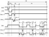
图3为图2所示像素电路的一种工作时序图,如图3所示,在四个阶段的工作过程如下:Fig. 3 is a working timing diagram of the pixel circuit shown in Fig. 2. As shown in Fig. 3, the working process in the four stages is as follows:
在重置阶段S1,重置控制线RST提供的重置控制信号处于低电平,补偿控制线CPS提供的补偿控制信号处于高电平状态,发光控制线EM提供的发光控制信号处于高电平状态,第一栅线Gate_A提供的栅极驱动信号处于高电平状态,数据线提供初始电压Vref。此时,第二晶体管T2导通,第一晶体管T1、第三晶体管T3和第四晶体管T4均截止。In the reset phase S1, the reset control signal provided by the reset control line RST is at a low level, the compensation control signal provided by the compensation control line CPS is in a high level state, and the light-emitting control signal provided by the light-emitting control line EM is at a high level In the state, the gate driving signal provided by the first gate line Gate_A is in a high level state, and the data line provides the initial voltage Vref. At this time, the second transistor T2 is turned on, and the first transistor T1 , the third transistor T3 and the fourth transistor T4 are all turned off.
由于第二晶体管T2导通,则重置电压Vint通过第二晶体管T2写入至控制节点N1,控制节点N1的电压为Vint。Since the second transistor T2 is turned on, the reset voltage Vint is written to the control node N1 through the second transistor T2, and the voltage of the control node N1 is Vint.
在补偿阶段S2,重置控制线RST提供的重置控制信号处于高电平,补偿控制线CPS提供的补偿控制信号处于低电平状态,发光控制线EM提供的发光控制信号处于高电平状态,第一栅线Gate_A提供的栅极驱动信号处于低电平状态,数据线提供初始电压Vref。此时,第一晶体管T1和第三晶体管T3均导通,第二晶体管T2和第四晶体管T4均截止。In the compensation stage S2, the reset control signal provided by the reset control line RST is at a high level, the compensation control signal provided by the compensation control line CPS is at a low level state, and the lighting control signal provided by the light-emitting control line EM is at a high level state , the gate driving signal provided by the first gate line Gate_A is in a low level state, and the data line provides the initial voltage Vref. At this time, the first transistor T1 and the third transistor T3 are both turned on, and the second transistor T2 and the fourth transistor T4 are both turned off.
由于第三晶体管T3导通,因此初始电压Vref通过第三晶体管T3写入至节点N2,节点N2的电压为Vref。又由于第一晶体管T1导通,则驱动晶体管DTFT输出电流并通过第一晶体管T1对控制节点N1进行充电,控制节点N1处的电压由Vint上升,直至控制节点N1处的电压上升至Vdd+Vth时驱动晶体管DTFT截止,充电结束,完成对驱动晶体管DTFT的阈值补偿处理;其中,Vth为驱动晶体管DTFT的阈值电压(Vth一般小于0V)。在补偿阶段S2结束时,第一电容C1的两端电压差为Vref-Vdd-Vth。Since the third transistor T3 is turned on, the initial voltage Vref is written to the node N2 through the third transistor T3, and the voltage of the node N2 is Vref. Since the first transistor T1 is turned on, the driving transistor DTFT outputs current and charges the control node N1 through the first transistor T1, and the voltage at the control node N1 rises from Vint until the voltage at the control node N1 rises to Vdd+Vth When the driving transistor DTFT is turned off, the charging is completed, and the threshold compensation processing of the driving transistor DTFT is completed; wherein, Vth is the threshold voltage of the driving transistor DTFT (Vth is generally less than 0V). At the end of the compensation phase S2, the voltage difference between the two ends of the first capacitor C1 is Vref-Vdd-Vth.
在驱动阶段S3,其包括多个驱动子阶段;在该像素电路所对应的一个驱动子阶段中,重置控制线RST提供的重置控制信号处于高电平,补偿控制线CPS提供的补偿控制信号处于高电平状态,发光控制线EM提供的发光控制信号处于高电平状态,第一栅线Gate_A提供的栅极驱动信号处于低电平状态,数据线提供数据电压Vdata_I。此时,第三晶体管T3导通,第一晶体管T1、第二晶体管T2和第四晶体管T4均截止In the driving stage S3, it includes a plurality of driving sub-stages; in a driving sub-stage corresponding to the pixel circuit, the reset control signal provided by the reset control line RST is at a high level, and the compensation control provided by the compensation control line CPS is at a high level. The signal is in a high-level state, the light-emitting control signal provided by the light-emitting control line EM is in a high-level state, the gate driving signal provided by the first gate line Gate_A is in a low-level state, and the data line provides the data voltage Vdata_I. At this time, the third transistor T3 is turned on, and the first transistor T1, the second transistor T2 and the fourth transistor T4 are all turned off
由于第一晶体管T1和第二晶体管T2截止,因此控制节点N1处于浮接(Floating)状态。与此同时,由于第三晶体管T3导通,因此数据电压Vdata_I通过第三晶体管T3写入至节点N2,在第一电容C1的自举作用下,控制节点N1的电压由Vdd+Vth跳变为Vdd+Vth+Vdata_I-Vref,此时驱动晶体管DTFT的栅源电压Vgs=Vth+Vdata_I-Vref,由于Vdata_I-Vref<0,因此Vgs<Vth。Since the first transistor T1 and the second transistor T2 are turned off, the control node N1 is in a floating state. At the same time, since the third transistor T3 is turned on, the data voltage Vdata_I is written to the node N2 through the third transistor T3. Under the bootstrapping action of the first capacitor C1, the voltage of the control node N1 jumps from Vdd+Vth to Vdd+Vth+Vdata_I-Vref, at this time, the gate-source voltage of the driving transistor DTFT is Vgs=Vth+Vdata_I-Vref. Since Vdata_I-Vref<0, Vgs<Vth.
需要说明的是,当驱动子阶段ti既不为驱动阶段S3中的第1个驱动子阶段,也不为驱动阶段S3中最后1个驱动子阶段时,则在驱动子阶段ti之前的其他驱动子阶段中,第一栅线Gate_A提供的栅极驱动信号处于高电平状态,因此节点N2处于浮接状态,节点N1处的电压维持在补偿阶段S2结束时的Vref。在驱动子阶段ti之后的其他驱动子阶段中,第一栅线Gate_A提供的栅极驱动信号处于高电平状态,因此节点N2处于浮接状态,节点N2处的电压维持在驱动子阶段ti结束时的Vdd+Vth+Vdata_I-Vref。It should be noted that when the driving sub-stage ti is neither the first driving sub-stage in the driving stage S3 nor the last driving sub-stage in the driving stage S3, the In other driving sub-stages, the gate driving signal provided by the first gate line Gate_A is in a high level state, so the node N2 is in a floating state, and the voltage at the node N1 is maintained at Vref at the end of the compensation stage S2. In other driving sub-stages after the driving sub-stage ti , the gate driving signal provided by the first gate line Gate_A is in a high-level state, so the node N2 is in a floating state, and the voltage at the node N2 is maintained at the driving sub-stage t Vdd+Vth+Vdata_I-Vref at the end ofi .
当驱动子阶段ti为驱动阶段S3中的第1个驱动子阶段时,则在驱动子阶段ti与补偿阶段S2之间不存在其他驱动子阶段。当驱动子阶段ti为驱动阶段S3中的最后1个驱动子阶段时,则在驱动子阶段ti与显示阶段S4之间不存在其他驱动子阶段。When the driving sub-phaseti is the first driving sub-phase in the driving phase S3, there are no other driving sub-phases between the driving sub-phaseti and the compensation phase S2. When the driving sub-phaseti is the last driving sub-phase in the driving phase S3, there is no other driving sub-phase between the driving sub-phaseti and the display phase S4.
在显示阶段S4,重置控制线RST提供的重置控制信号处于高电平,补偿控制线CPS提供的补偿控制信号处于高电平状态,发光控制线EM提供的发光控制信号处于低电平状态,第一栅线Gate_A提供的栅极驱动信号处于高电平状态,数据线提供初始电压Vref。此时,第四晶体管T4导通,第一晶体管T1、第二晶体管T2和第三晶体管T3均截止。In the display stage S4, the reset control signal provided by the reset control line RST is at a high level, the compensation control signal provided by the compensation control line CPS is at a high level state, and the lighting control signal provided by the light-emitting control line EM is at a low level state , the gate driving signal provided by the first gate line Gate_A is in a high level state, and the data line provides the initial voltage Vref. At this time, the fourth transistor T4 is turned on, and the first transistor T1 , the second transistor T2 and the third transistor T3 are all turned off.
由于此时驱动晶体管DTFT的栅源电压Vgs<Vth,因此驱动晶体管DTFT导通。根据由驱动晶体管DTFT的饱和驱动电流公式可得:Since the gate-source voltage Vgs<Vth of the driving transistor DTFT at this time, the driving transistor DTFT is turned on. According to the saturated driving current formula of the driving transistor DTFT, it can be obtained:
I=K*(Vgs-Vth)2I=K*(Vgs-Vth)2
=K*(Vth+Vdata_I-Vref-Vth)2=K*(Vth+Vdata_I-Vref-Vth)2
=K*(Vdata_I-Vref)2=K*(Vdata_I-Vref)2
其中,K为一个常量,由驱动晶体管DTFT的电学特性决定。通过上式可知,驱动晶体管DTFT的驱动电流仅与数据电压和参考电压相关,而与驱动晶体管DTFT的阈值电压Vth无关,从而可避免流过发光器件LED的驱动电流受到阈值电压不均匀和漂移的影响,进而有效的提高了流过发光器件LED的驱动电流的均匀性。Among them, K is a constant, which is determined by the electrical characteristics of the driving transistor DTFT. It can be seen from the above formula that the driving current of the driving transistor DTFT is only related to the data voltage and the reference voltage, but has nothing to do with the threshold voltage Vth of the driving transistor DTFT, so that the driving current flowing through the light-emitting device LED can be prevented from being affected by the unevenness and drift of the threshold voltage. Therefore, the uniformity of the driving current flowing through the light-emitting device LED is effectively improved.
需要说明的是,发光控制线EM提供的发光控制信号在整个显示阶段S4均处于低电平状态的情况,仅为本公开中的一种可选方案,在本公开中,发光控制信号可在显示阶段S4中的至少部分时间段处于低电平即可。It should be noted that the case where the light-emitting control signal provided by the light-emitting control line EM is in a low-level state during the entire display stage S4 is only an optional solution in the present disclosure. In the present disclosure, the light-emitting control signal can be It is sufficient that at least part of the time period in the display stage S4 is at a low level.
作为一种应用场景,发光控制信号在显示阶段S4中部分时间段处于低电平状态,通过控制发光控制信号在显示阶段S4内处于低电平状态的时长,可以实现对发光器件LED在一帧中的等效亮度进行控制,以实现更为丰富的亮度调节。As an application scenario, the light-emitting control signal is in a low-level state for part of the time period in the display stage S4, and by controlling the duration of the light-emitting control signal in the low-level state in the display stage S4, it is possible to realize the control of the light-emitting device LED in one frame. Control the equivalent brightness in , to achieve richer brightness adjustment.
作为又一种应用场景,在增大驱动晶体管DTFT所输出驱动电流(调整Vdata_I的大小)的同时,控制发光控制信号在显示阶段S4中多次进行高/低电平的切换(发光器件LED在显示阶段S4中多次进行点亮/熄灭的切换),且使得发光器件LED在一帧中的等效亮度等于期望亮度。在上述过程中,由于驱动晶体管DTFT所输出的电流为大电流(高电流密度),发光器件LED在点亮状态时始终处于高灰阶状态,因此发光器件LED的具有较高的发光效率,且不会出现色偏的问题,As another application scenario, while increasing the driving current output by the driving transistor DTFT (adjusting the size of Vdata_I), the light-emitting control signal is controlled to perform high/low switching multiple times in the display stage S4 (the light-emitting device LED is in the display stage S4). Switching on/off is performed multiple times in the display stage S4), and the equivalent brightness of the light emitting device LED in one frame is made equal to the desired brightness. In the above process, since the current output by the driving transistor DTFT is a large current (high current density), the light-emitting device LED is always in a high gray-scale state when it is on, so the light-emitting device LED has a high luminous efficiency, and There will be no color cast problem.
图4为本公开实施例提供的像素电路的另一种电路结构示意图,如图4所示,与图2所示像素电路不同的是,本实施例中的发光控制电路4不仅包括第四晶体管T4,还包括第五晶体管T5、第六晶体管T6和第二电容C2。FIG. 4 is a schematic diagram of another circuit structure of a pixel circuit provided by an embodiment of the present disclosure. As shown in FIG. 4 , different from the pixel circuit shown in FIG. 2 , the light-emitting
其中,第四晶体管T4的控制极与发光控制线EM连接,第四晶体管T4的第一极与驱动晶体管DTFT的第二极连接,第四晶体管T4的第二极与第六晶体管T6的第一极连接。The control electrode of the fourth transistor T4 is connected to the light-emitting control line EM, the first electrode of the fourth transistor T4 is connected to the second electrode of the driving transistor DTFT, and the second electrode of the fourth transistor T4 is connected to the first electrode of the sixth transistor T6 pole connection.
第五晶体管T5的控制极与第二栅线Gate_B连接,第五晶体管T5的第一极与第二数据线Data_T连接,第五晶体管T5的第二极与第六晶体管T6的控制极连接;The control electrode of the fifth transistor T5 is connected to the second gate line Gate_B, the first electrode of the fifth transistor T5 is connected to the second data line Data_T, and the second electrode of the fifth transistor T5 is connected to the control electrode of the sixth transistor T6;
第六晶体管T6的控制极与第二电容C2的第一端连接,第六晶体管T6的第二极与发光器件LED的第一端连接;第二电容C2的第二端与公共电源端连接。其中,公共电源端提供公共电压Vcom。The control electrode of the sixth transistor T6 is connected to the first end of the second capacitor C2, the second electrode of the sixth transistor T6 is connected to the first end of the light emitting device LED; the second end of the second capacitor C2 is connected to the common power supply end. The common power supply terminal provides the common voltage Vcom.
图5为图4所示像素电路的一种工作时序图,如图5所示,在四个阶段的工作过程如下:Fig. 5 is a working timing diagram of the pixel circuit shown in Fig. 4. As shown in Fig. 5, the working process in the four stages is as follows:
基于图5所示的工作时序,图4所示像素电路在重置阶段S1、补偿阶段S2和驱动阶段S3的工作过程,与图2所示像素电路基于图3所述工作时序时在重置阶段S1、补偿阶段S2和驱动阶段S3的工作过程相同,此处不再赘述。下面仅对显示阶段S4进行详细描述。Based on the working sequence shown in FIG. 5 , the working process of the pixel circuit shown in FIG. 4 in the reset stage S1 , the compensation stage S2 and the driving stage S3 is different from the working process of the pixel circuit shown in FIG. 2 based on the working sequence shown in FIG. The working processes of the stage S1 , the compensation stage S2 and the driving stage S3 are the same, and will not be repeated here. Only the display stage S4 will be described in detail below.
在本实施例中,显示阶段S4包括:交替进行的多个扫描周期U1~Um和非发光周期U1’~Um’。需要说明的是,各扫描周期U1~Um的时长可以相同,也可以不同;各非发光周期U1’~Um’的时长可以相同也可以不同。仅需保证在每个扫描周期U1~Um内,显示装置中的全部第二栅线Gate_B均能完成扫描即可。In this embodiment, the display stage S4 includes: a plurality of scanning periods U1-Um and non-light-emitting periods U1'-Um' which are performed alternately. It should be noted that the duration of each scanning period U1-Um may be the same or different; the duration of each non-light-emitting period U1'-Um' may be the same or different. It only needs to ensure that all the second gate lines Gate_B in the display device can complete the scanning in each scanning period U1-Um.
其中,在非发光周期U1’~Um’内,发光控制线EM提供的发光控制信号始终处于高电平状态,因此第四晶体管T4截止,驱动晶体管DTFT无法向发光器件LED提供驱动电流,发光器件LED不发光。Among them, in the non-light-emitting period U1'-Um', the light-emitting control signal provided by the light-emitting control line EM is always in a high-level state, so the fourth transistor T4 is turned off, and the driving transistor DTFT cannot provide the driving current to the light-emitting device LED. LEDs do not emit light.
在每个扫描周期U1~Um内,均至少包括多个扫描子阶段,每个扫描子阶段对应显示面板上的一行像素单元。在本实施例中,假定图4所示像素电路对应扫描周期内的第i个扫描子阶段pi,即该像素电路所连接的第二栅线Gate_B所提供的扫描信号在扫描子阶段pi处于低电平状态,而在一帧中的其他时间处于高电平状态;即第五晶体管T5仅在对应的扫描子阶段pi时处于导通状态,而在一帧中的其他时间处于截止状态。Each scanning period U1-Um includes at least a plurality of scanning sub-stages, and each scanning sub-stage corresponds to a row of pixel units on the display panel. In this embodiment, it is assumed that the pixel circuit shown in FIG. 4 corresponds to the i-th scanning sub-stage pi in the scanning period, that is, the scanning signal provided by the second gate line Gate_B connected to the pixel circuit is in the scanning sub-stage pi is in a low-level state, and is in a high-level state at other times in a frame; that is, the fifth transistor T5 is only in an on state during the corresponding scanning sub-phase pi , and is in an off state at other times in a frame state.
在像素电路所对应的各扫描子阶段pi中,第二数据线Data_T提供数据电压Vdata_T,其中Vdata_T可以为高电平电压也可以为低电平电压(根据需要进行选择)。In each scanning sub-phase pi corresponding to the pixel circuit, the second data lineData_T provides a data voltage Vdata_T, wherein Vdata_T can be a high-level voltage or a low-level voltage (selected as required).
其中,当Vdata_T为低电平电压时,则Vdata_T通过第五晶体管T5写入至第六晶体管T6的控制极,第六晶体管T6导通,驱动晶体管DTFT的第二极与发光器件LED的第一极之间导通,驱动晶体管DTFT输出的驱动电流依次通过第四晶体管T4、第六晶体管T6流入至发光器件LED,发光器件LED发光。在扫描子阶段pi结束至下一个非发光周期开始之间的时间段内,第六晶体管T6的控制极处于浮接状态,第六晶体管T6维持导通,发光器件LED维持发光。Wherein, when Vdata_T is a low-level voltage, Vdata_T is written to the control electrode of the sixth transistor T6 through the fifth transistor T5, the sixth transistor T6 is turned on, and the second electrode of the driving transistor DTFT is connected to the first electrode of the light-emitting device LED. The electrodes are turned on, and the driving current output by the driving transistor DTFT flows into the light-emitting device LED through the fourth transistor T4 and the sixth transistor T6 in sequence, and the light-emitting device LED emits light. During the time period between the end of the scanning sub-phase pi and the start of the next non-light-emitting period, the control electrode of the sixth transistor T6 is in a floating state, the sixth transistor T6 is kept on, and the light-emitting device LED keeps light-emitting.
当Vdata_T为高电平电压时,则Vdata_T通过第五晶体管T5写入至第六晶体管T6的控制极,第六晶体管T6截止,驱动晶体管DTFT的第二极与发光器件LED的第一极之间断路,发光器件LED不发光。When Vdata_T is a high-level voltage, Vdata_T is written to the control electrode of the sixth transistor T6 through the fifth transistor T5, the sixth transistor T6 is turned off, and the second electrode of the driving transistor DTFT is disconnected from the first electrode of the light emitting device LED. Road, the light-emitting device LED does not emit light.
因此,在每个扫描周期内,通过控制该像素电路所连接的第二数据线Data_T所提供的Vdata_T的大小,从而可对该像素电路在各扫描周期内是否发光进行有效控制。Therefore, in each scan period, by controlling the magnitude of Vdata_T provided by the second data line Data_T connected to the pixel circuit, whether the pixel circuit emits light in each scan period can be effectively controlled.
需要说明的是,在本公开中,每个扫描周期的时长可以相等,也可以不等,其均属于本公开的保护范围。It should be noted that, in the present disclosure, the duration of each scan period may be equal or unequal, which all belong to the protection scope of the present disclosure.
在本实施例中,在显示阶段S4内,通过发光控制信号线所提供的发光控制信号、第二数据线Data_T提供的数据电压Vdata_T,可对发光器件LED在显示阶段S4的发光时间进行有效控制。In this embodiment, in the display stage S4, the light-emitting time of the light-emitting device LED in the display stage S4 can be effectively controlled by the light-emitting control signal provided by the light-emitting control signal line and the data voltage Vdata_T provided by the second data line Data_T .
图6为图4所示像素电路的另一种工作时序图,如图6所示,与图5中不同的是,图6所示显示阶段S4在补偿阶段S2结束后与驱动阶段S3同步开始,从而能进一步提升显示阶段S4的总时长。FIG. 6 is another working timing diagram of the pixel circuit shown in FIG. 4. As shown in FIG. 6, the difference from FIG. 5 is that the display stage S4 shown in FIG. 6 starts synchronously with the driving stage S3 after the compensation stage S2 ends. , so that the total duration of the display stage S4 can be further increased.
对于图4所示像素电路基于图6所示工作时序在重置阶段S1、补偿阶段S2、驱动阶段S3和显示阶段S4的工作过程,可参见前述内容,此处不再赘述。For the working process of the pixel circuit shown in FIG. 4 in the reset stage S1 , the compensation stage S2 , the driving stage S3 and the display stage S4 based on the working sequence shown in FIG.
需要说明的是,上述各实施例所提供的像素电路中的全部晶体管均为P型晶体管的情况,其为本公开中的一种优选方案,其可使得像素电路中的全部晶体管采用相同制备工艺进行制备,有效缩短制备周期。同理,像素电路中的全部晶体管均为N型晶体管,也可实现相同的技术效果。It should be noted that the case where all the transistors in the pixel circuit provided by the above embodiments are P-type transistors is a preferred solution in the present disclosure, which enables all the transistors in the pixel circuit to use the same fabrication process Preparation, effectively shorten the preparation cycle. Similarly, all transistors in the pixel circuit are N-type transistors, and the same technical effect can also be achieved.
图7为本公开实施例提供的一种显示装置的电路结构示意图,如图7所示,该显示装置包括:显示基板,显示基板上包括多个发光器件LED,多个发光器件LED中的至少一个与前述任一实施例提供的一个像素电路PIX连接。对于像素电路PIX的具体描述,可参见前述实施例中的内容,此处不再赘述。FIG. 7 is a schematic diagram of a circuit structure of a display device according to an embodiment of the present disclosure. As shown in FIG. 7 , the display device includes: a display substrate, and the display substrate includes a plurality of light-emitting device LEDs, at least one of the plurality of light-emitting device LEDs One is connected to a pixel circuit PIX provided in any of the foregoing embodiments. For the specific description of the pixel circuit PIX, reference may be made to the content in the foregoing embodiments, which will not be repeated here.
在一些实施例中,像素电路PIX的数量大于或等于2个;需要说明的是,图7中示例性画出了4个像素电路PIX,且像素电路PIX采用图4中所示,该情况仅起到示例性作用,不会对本公开的技术方案产生限制。In some embodiments, the number of pixel circuits PIX is greater than or equal to 2; it should be noted that 4 pixel circuits PIX are exemplarily drawn in FIG. 7 , and the pixel circuits PIX shown in FIG. It serves as an example and does not limit the technical solutions of the present disclosure.
在多个像素电路PIX所构成的像素阵列中,位于同一行的像素电路PIX对应同一条第一栅线Gate_A(1)/Gate_A(2),位于同一列的像素电路PIX对应同一条第一数据线Data_I(1)/Data_I(2)/Data_I(3)。In a pixel array formed by a plurality of pixel circuits PIX, the pixel circuits PIX located in the same row correspond to the same first gate line Gate_A(1)/Gate_A(2), and the pixel circuits PIX located in the same column correspond to the same first data Line Data_I(1)/Data_I(2)/Data_I(3).
需要说明的是,图7所示显示装置中仅示例性画出了2条第一栅线Gate_A(1)/Gate_A(2)和3条第一数据线Data_I(1)/Data_I(2)/Data_I(3),该情况仅起到示例性作用,不会对本公开的技术方案产生限制。It should be noted that, in the display device shown in FIG. 7 , only two first gate lines Gate_A(1)/Gate_A(2) and three first data lines Data_I(1)/Data_I(2)/ Data_I(3), this situation only serves as an example, and will not limit the technical solution of the present disclosure.
在一些实施例中,显示装置中的至少两个像素电路PIX所连接的重置控制线RST为同一重置控制线RST,至少两个像素电路PIX所连接的补偿控制线CPS为同一补偿控制线CPS,至少两个像素电路PIX所连接的发光控制线EM为同一发光控制线EM。In some embodiments, the reset control line RST connected to at least two pixel circuits PIX in the display device is the same reset control line RST, and the compensation control line CPS connected to the at least two pixel circuits PIX is the same compensation control line CPS, the light-emitting control lines EM connected to at least two pixel circuits PIX are the same light-emitting control line EM.
进一步可选地,显示装置中每一个像素电路PIX对应的重置控制线RST均与其他像素电路PIX对应的重置控制线RST电连接,每一个像素电路PIX对应的补偿控制线CPS均与其他像素电路PIX对应的补偿控制线CPS电连接,每一个像素电路PIX对应的发光控制线EM均与其他像素电路PIX对应的发光控制线EM电连接。此时,通过该同一重置控制线RST可以控制全部像素电路PIX同时对各自内部的控制节点N1进行重置处理,通过该同一补偿控制线CPS可以控制全部像素电路PIX同时对各自内部的驱动晶体管DTFT进行阈值补偿处理。Further optionally, the reset control line RST corresponding to each pixel circuit PIX in the display device is electrically connected to the reset control line RST corresponding to other pixel circuits PIX, and the compensation control line CPS corresponding to each pixel circuit PIX is connected to other pixel circuits PIX. The compensation control lines CPS corresponding to the pixel circuits PIX are electrically connected, and the light emission control lines EM corresponding to each pixel circuit PIX are electrically connected to the light emission control lines EM corresponding to other pixel circuits PIX. At this time, all pixel circuits PIX can be controlled by the same reset control line RST to perform reset processing on the respective internal control nodes N1, and all pixel circuits PIX can be controlled by the same compensation control line CPS simultaneously. DTFT performs threshold compensation processing.
在本实施例中,假定一帧时间为T,驱动阶段包括n个驱动子阶段(n≥2),在第i个驱动子阶段内,显示面板中位于第i行的像素电路完成数据电压写入操作操作;另外,像素电路完成数据电压写入操作所需的最小时长为Td,像素电路完成对驱动晶体管DTFT的阈值补偿操作所需的最小时长为Tc,像素电路完成对控制节点N1的重置操作所需最小时长为Ta(Ta近似等于Td)。In this embodiment, assuming that one frame time is T, the driving stage includes n driving sub-stages (n≥2). In the i-th driving sub-stage, the pixel circuit in the i-th row in the display panel completes data voltage writing In addition, the minimum time required for the pixel circuit to complete the data voltage writing operation is Td, the minimum time required for the pixel circuit to complete the threshold compensation operation for the driving transistor DTFT is Tc, and the pixel circuit completes the control node N1. The minimum time required for the set operation is Ta (Ta is approximately equal to Td).
在本公开中,重置阶段、补偿阶段和驱动阶段三个阶段的最小时长之和为Ta+Tc+n*Td,显示阶段的最大时长为T-(Ta+Tc+n*Td)。而在相关技术中,驱动阶段的最小总时长为n*Tc,显示阶段的最大时长为T-n*Tc。由于Ta近似等于Td,Tc一般为Td的4倍,因此Ta+Tc+n*Td<n*Tc,T-(Ta+Tc+n*Td)>T-n*Tc;所以,采用本公开所提供的技术方案,可使得一帧内显示阶段S4的时长提升,有利于提升发光器件LED的发光效率。In the present disclosure, the sum of the minimum durations of the reset phase, the compensation phase and the driving phase is Ta+Tc+n*Td, and the maximum duration of the display phase is T-(Ta+Tc+n*Td). In the related art, the minimum total duration of the driving phase is n*Tc, and the maximum duration of the display phase is T-n*Tc. Since Ta is approximately equal to Td, Tc is generally 4 times of Td, so Ta+Tc+n*Td<n*Tc, T-(Ta+Tc+n*Td)>T-n*Tc; The technical solution can increase the duration of the display stage S4 in one frame, which is beneficial to improve the luminous efficiency of the light-emitting device LED.
需要说明的是,当显示基板中的像素电路包括第五晶体管T5和第六晶体管T6时,位于同一行的像素电路PIX对应同一条第二栅线Gate_B(1)/Gate_B(2),位于同一列的像素电路对应同一条第二数据线Data_T(1)/Data_T(2)/Data_T(3)。It should be noted that when the pixel circuit in the display substrate includes the fifth transistor T5 and the sixth transistor T6, the pixel circuits PIX located in the same row correspond to the same second gate line Gate_B(1)/Gate_B(2), and are located in the same second gate line Gate_B(1)/Gate_B(2). The pixel circuits of the columns correspond to the same second data line Data_T(1)/Data_T(2)/Data_T(3).
图8为本公开实施例提供的像素电路的驱动方法的一种流程图,如图8所示,该驱动方法为对应一个像素电路的驱动方法,该像素电路采用前述任一实施例所提供的像素电路,对于该像素电路的描述可参见前述实施例中的内容。该一个像素电路的驱动方法包括:FIG. 8 is a flowchart of a method for driving a pixel circuit provided by an embodiment of the present disclosure. As shown in FIG. 8 , the driving method corresponds to a driving method for a pixel circuit, and the pixel circuit adopts the method provided by any of the foregoing embodiments. Pixel circuit, for the description of the pixel circuit, reference may be made to the content in the foregoing embodiments. The driving method of the one pixel circuit includes:
步骤S101、在重置阶段,发光控制电路在重置控制线的控制下,控制驱动晶体管的第二极与发光器件的第一极之间形成断路;以及,重置电路在重置控制线的控制下,将重置电源端所提供的重置电压写入至控制节点。Step S101, in the reset stage, under the control of the reset control line, the light emitting control circuit controls to form an open circuit between the second pole of the driving transistor and the first pole of the light emitting device; Under the control, the reset voltage provided by the reset power terminal is written to the control node.
步骤S102、在补偿阶段,发光控制电路在重置控制线的控制下,控制驱动晶体管的第二极与发光器件的第一极之间形成断路;以及,阈值补偿电路在补偿控制线的控制下,对驱动晶体管进行阈值补偿。Step S102, in the compensation stage, the light-emitting control circuit controls the second pole of the driving transistor and the first pole of the light-emitting device to form an open circuit under the control of the reset control line; and, the threshold compensation circuit is under the control of the compensation control line , to perform threshold compensation on the drive transistor.
步骤S103、在驱动阶段中的一个驱动子阶段,数据写入电路在第一栅线的控制下,根据第一数据线所提供的数据电压来对控制节点进行充电。Step S103 , in a driving sub-stage in the driving stage, the data writing circuit, under the control of the first gate line, charges the control node according to the data voltage provided by the first data line.
步骤S103中的“一个驱动子阶段”是指该像素电路所对应的一个驱动子阶段(第一栅线提供的驱动信号处于有效电平状态)。"One driving sub-stage" in step S103 refers to one driving sub-stage corresponding to the pixel circuit (the driving signal provided by the first gate line is in an active level state).
步骤S104、在显示阶段中的至少部分时间段,发光控制电路在发光控制信号线的控制下,控制驱动晶体管的第二极与发光器件的第一极之间的通路,驱动晶体管根据控制节点处的电压输出相应的驱动电流。Step S104: During at least part of the time period in the display stage, the light-emitting control circuit controls the path between the second pole of the driving transistor and the first pole of the light-emitting device under the control of the light-emitting control signal line, and the driving transistor is controlled according to the position of the control node. The voltage outputs the corresponding drive current.
对于上述步骤S101~步骤S104的具体描述,可参见前述对像素电路工作过程的描述内容,此处不再赘述。For the specific description of the above steps S101 to S104, reference may be made to the foregoing description of the working process of the pixel circuit, which will not be repeated here.
图9为本公开实施例提供的多个像素电路的驱动方法的一种流程图,如图9所示,该多个像素电路对应于至少两条第一栅线,其中每个像素电路均采用前述任一实施例所提供的像素电路。该多个像素电路的驱动方法包括:FIG. 9 is a flowchart of a method for driving multiple pixel circuits according to an embodiment of the present disclosure. As shown in FIG. 9 , the multiple pixel circuits correspond to at least two first gate lines, and each pixel circuit adopts The pixel circuit provided by any of the foregoing embodiments. The driving method of the plurality of pixel circuits includes:
步骤S201、在重置阶段,全部像素电路内的发光控制电路同时在重置控制线的控制下,控制各像素电路内的驱动晶体管的第二极与发光器件的第一极之间形成断路;以及,全部像素电路内的重置电路在重置控制线的控制下,将重置电源端所提供的重置电压写入至各像素电路内的控制节点。Step S201 , in the reset stage, under the control of the reset control line, the light-emitting control circuits in all pixel circuits simultaneously control the second pole of the driving transistor in each pixel circuit to form an open circuit between the second pole of the driving transistor and the first pole of the light-emitting device; And, under the control of the reset control line, the reset circuits in all the pixel circuits write the reset voltage provided by the reset power supply terminal into the control nodes in each pixel circuit.
步骤S202、在补偿阶段,全部像素电路内的发光控制电路同时在重置控制线的控制下,维持各像素电路内驱动晶体管的第二极与发光器件的第一极之间的断路状态;以及,全部像素电路内的阈值补偿电路同时在补偿控制线的控制下,对各像素电路内的驱动晶体管进行阈值补偿。Step S202, in the compensation stage, the light-emitting control circuits in all pixel circuits are simultaneously controlled by the reset control line to maintain the open-circuit state between the second pole of the driving transistor and the first pole of the light-emitting device in each pixel circuit; and , the threshold compensation circuits in all pixel circuits simultaneously perform threshold compensation on the driving transistors in each pixel circuit under the control of the compensation control line.
步骤S203、在驱动阶段,包括依次进行的多个驱动子阶段,其中在任意一个驱动子阶段内,与该驱动子阶段所对应的像素电路内的数据写入电路在对应的第一栅线的控制下,根据对应的第一数据线所提供的数据电压来对控制节点进行充电。Step S203, in the driving stage, including a plurality of driving sub-stages performed in sequence, wherein in any driving sub-stage, the data writing circuit in the pixel circuit corresponding to the driving sub-stage is in the corresponding first gate line. Under the control, the control node is charged according to the data voltage provided by the corresponding first data line.
步骤S204、在显示阶段中的至少部分时间段,全部像素电路内的发光控制电路在发光控制信号线的控制下,控制控制各像素电路内的驱动晶体管的第二极与发光器件的第一极之间的通路,各像素电路内的驱动晶体管根据控制节点处的电压输出相应的驱动电流。Step S204: During at least part of the time period in the display stage, the light-emitting control circuits in all pixel circuits, under the control of the light-emitting control signal lines, control the second electrode of the driving transistor in each pixel circuit and the first electrode of the light-emitting device. The path between them, the driving transistor in each pixel circuit outputs the corresponding driving current according to the voltage at the control node.
对于上述步骤S201~步骤S204的具体描述,可参见前述对像素电路和显示装置的工作过程的描述内容,此处不再赘述。For the specific description of the above steps S201 to S204, reference may be made to the foregoing description of the working process of the pixel circuit and the display device, which will not be repeated here.
本公开的技术方案,通过对显示装置中的像素电路进行重新设计,可使得显示装置中的像素电路同时进行对驱动晶体管的阈值补偿处理,以使得补偿阶段和驱动阶段的时长之和小于相关技术中驱动阶段的总时长,从而使得一帧中显示阶段的时长得到提升,有利于提升发光器件的发光效率。According to the technical solution of the present disclosure, by redesigning the pixel circuit in the display device, the pixel circuit in the display device can simultaneously perform threshold compensation processing on the driving transistor, so that the sum of the durations of the compensation phase and the driving phase is smaller than that of the related art The total duration of the middle driving stage is increased, so that the duration of the display stage in one frame is increased, which is beneficial to improve the luminous efficiency of the light emitting device.
可以理解的是,以上实施方式仅仅是为了说明本发明的原理而采用的示例性实施方式,然而本发明并不局限于此。对于本领域内的普通技术人员而言,在不脱离本发明的精神和实质的情况下,可以做出各种变型和改进,这些变型和改进也视为本发明的保护范围。It can be understood that the above embodiments are only exemplary embodiments adopted to illustrate the principle of the present invention, but the present invention is not limited thereto. For those skilled in the art, without departing from the spirit and essence of the present invention, various modifications and improvements can be made, and these modifications and improvements are also regarded as the protection scope of the present invention.
Claims (9)
Priority Applications (3)
| Application Number | Priority Date | Filing Date | Title |
|---|---|---|---|
| CN201910599791.7ACN112259041B (en) | 2019-07-04 | 2019-07-04 | Pixel circuit and driving method thereof, and display device |
| US17/255,523US11100851B2 (en) | 2019-07-04 | 2020-06-29 | Pixel circuit and driving method thereof, display device |
| PCT/CN2020/098723WO2021000816A1 (en) | 2019-07-04 | 2020-06-29 | Pixel circuit and driving method therefor, and display device |
Applications Claiming Priority (1)
| Application Number | Priority Date | Filing Date | Title |
|---|---|---|---|
| CN201910599791.7ACN112259041B (en) | 2019-07-04 | 2019-07-04 | Pixel circuit and driving method thereof, and display device |
Publications (2)
| Publication Number | Publication Date |
|---|---|
| CN112259041A CN112259041A (en) | 2021-01-22 |
| CN112259041Btrue CN112259041B (en) | 2022-09-09 |
Family
ID=74101207
Family Applications (1)
| Application Number | Title | Priority Date | Filing Date |
|---|---|---|---|
| CN201910599791.7AActiveCN112259041B (en) | 2019-07-04 | 2019-07-04 | Pixel circuit and driving method thereof, and display device |
Country Status (3)
| Country | Link |
|---|---|
| US (1) | US11100851B2 (en) |
| CN (1) | CN112259041B (en) |
| WO (1) | WO2021000816A1 (en) |
Families Citing this family (7)
| Publication number | Priority date | Publication date | Assignee | Title |
|---|---|---|---|---|
| CN112837649B (en)* | 2019-11-01 | 2022-10-11 | 京东方科技集团股份有限公司 | Pixel driving circuit, driving method thereof, display panel and display device |
| CN118248094A (en)* | 2020-10-15 | 2024-06-25 | 厦门天马微电子有限公司 | Pixel circuit, display panel, driving method of display panel and display device |
| US11605344B2 (en)* | 2020-10-15 | 2023-03-14 | Xiamen Tianma Micro-Electronics Co., Ltd. | Pixel circuit, display panel and driving method thereof, and display device |
| KR102828658B1 (en)* | 2021-11-10 | 2025-07-04 | 엘지디스플레이 주식회사 | Display device and data driving circuit |
| CN118974812A (en)* | 2023-02-20 | 2024-11-15 | 京东方科技集团股份有限公司 | Pixel circuit, display panel, display device and driving method |
| CN119137646A (en) | 2023-03-31 | 2024-12-13 | 京东方科技集团股份有限公司 | Display device and pixel circuit |
| CN120548565A (en)* | 2023-12-25 | 2025-08-26 | 京东方科技集团股份有限公司 | Pixel circuit, driving method and display device |
Family Cites Families (12)
| Publication number | Priority date | Publication date | Assignee | Title |
|---|---|---|---|---|
| KR101674479B1 (en)* | 2010-08-10 | 2016-11-10 | 삼성디스플레이 주식회사 | Organic Light Emitting Display Device |
| KR101706239B1 (en)* | 2010-12-22 | 2017-02-14 | 엘지디스플레이 주식회사 | Organic light emitting diode display device and method for driving the same |
| CN103296055B (en)* | 2012-12-26 | 2015-12-09 | 上海天马微电子有限公司 | Pixel circuit and driving method of organic light emitting display and organic light emitting display |
| KR102033611B1 (en)* | 2013-02-25 | 2019-10-18 | 삼성디스플레이 주식회사 | Pixel, display device including the same and method therof |
| US10424246B2 (en)* | 2015-07-21 | 2019-09-24 | Shenzhen Royole Technologies Co., Ltd. | Pixel circuit and method for driving pixel circuit |
| US10672338B2 (en)* | 2017-03-24 | 2020-06-02 | Apple Inc. | Organic light-emitting diode display with external compensation and anode reset |
| KR102470378B1 (en)* | 2017-11-30 | 2022-11-23 | 엘지디스플레이 주식회사 | Gate driving circuit and light emitting display apparatus comprising the same |
| KR102485163B1 (en)* | 2018-02-12 | 2023-01-09 | 삼성디스플레이 주식회사 | A display device |
| KR102533763B1 (en)* | 2018-03-27 | 2023-05-19 | 삼성디스플레이 주식회사 | Organic light emitting display device |
| CN108648674B (en)* | 2018-04-03 | 2019-08-02 | 京东方科技集团股份有限公司 | Display panel and driving method, display device |
| CN208488962U (en)* | 2018-08-06 | 2019-02-12 | 上海视涯信息科技有限公司 | A kind of pixel circuit and display device |
| CN109920371B (en)* | 2019-04-26 | 2021-01-29 | 京东方科技集团股份有限公司 | Pixel circuit and driving method thereof, and display device |
- 2019
- 2019-07-04CNCN201910599791.7Apatent/CN112259041B/enactiveActive
- 2020
- 2020-06-29USUS17/255,523patent/US11100851B2/enactiveActive
- 2020-06-29WOPCT/CN2020/098723patent/WO2021000816A1/ennot_activeCeased
Also Published As
| Publication number | Publication date |
|---|---|
| CN112259041A (en) | 2021-01-22 |
| WO2021000816A1 (en) | 2021-01-07 |
| US20210201773A1 (en) | 2021-07-01 |
| US11100851B2 (en) | 2021-08-24 |
Similar Documents
| Publication | Publication Date | Title |
|---|---|---|
| CN112259041B (en) | Pixel circuit and driving method thereof, and display device | |
| CN110660360B (en) | Pixel circuit and driving method thereof, and display panel | |
| CN103413520B (en) | Pixel-driving circuit, display device and image element driving method | |
| CN104751784B (en) | Organic light emitting display and its driving method | |
| CN108648696B (en) | Pixel circuit, array substrate, display device, and pixel driving method | |
| CN104658485B (en) | OLED driving compensation circuit and driving method thereof | |
| CN106952618B (en) | Display device and pixel circuit and its control method | |
| CN109509433A (en) | Pixel circuit, display device and image element driving method | |
| CN106991964A (en) | Image element circuit and its driving method, display device | |
| CN107833559B (en) | Pixel driving circuit, organic light emitting display panel and pixel driving method | |
| CN108447446A (en) | Pixel circuit, display panel and driving method thereof | |
| CN104700782B (en) | OELD pixel circuit, display device and control method | |
| CN106558287A (en) | Organic light emissive pixels drive circuit, driving method and organic electroluminescence display panel | |
| CN102930821B (en) | A kind of image element circuit and driving method, display device | |
| CN104575379B (en) | Display device and its driving method | |
| CN104715726A (en) | Pixel driving circuit, pixel driving method and display device | |
| CN109979394A (en) | Pixel circuit and its driving method, array substrate and display device | |
| CN104882099B (en) | A kind of pixel-driving circuit, array base palte and display device | |
| CN111754941B (en) | Pixel circuit, driving method thereof, display substrate and display device | |
| CN203376957U (en) | Pixel driving circuit and display device | |
| CN106683619A (en) | Pixel driving circuit, pixel driving method and display device | |
| CN106971691A (en) | A kind of image element circuit, driving method and display device | |
| CN107424564B (en) | Pixel device, driving method for pixel device, and display device | |
| CN106991976A (en) | Image element circuit, image element driving method and display device | |
| CN104978932A (en) | Pixel driving circuit, pixel driving method and display device |
Legal Events
| Date | Code | Title | Description |
|---|---|---|---|
| PB01 | Publication | ||
| PB01 | Publication | ||
| SE01 | Entry into force of request for substantive examination | ||
| SE01 | Entry into force of request for substantive examination | ||
| GR01 | Patent grant | ||
| GR01 | Patent grant |