CN112233621B - A pixel drive circuit, a display panel and an electronic device - Google Patents
A pixel drive circuit, a display panel and an electronic deviceDownload PDFInfo
- Publication number
- CN112233621B CN112233621BCN202011080105.4ACN202011080105ACN112233621BCN 112233621 BCN112233621 BCN 112233621BCN 202011080105 ACN202011080105 ACN 202011080105ACN 112233621 BCN112233621 BCN 112233621B
- Authority
- CN
- China
- Prior art keywords
- transistor
- light
- pole
- signal
- module
- Prior art date
- Legal status (The legal status is an assumption and is not a legal conclusion. Google has not performed a legal analysis and makes no representation as to the accuracy of the status listed.)
- Active
Links
Images


Classifications
- G—PHYSICS
- G09—EDUCATION; CRYPTOGRAPHY; DISPLAY; ADVERTISING; SEALS
- G09G—ARRANGEMENTS OR CIRCUITS FOR CONTROL OF INDICATING DEVICES USING STATIC MEANS TO PRESENT VARIABLE INFORMATION
- G09G3/00—Control arrangements or circuits, of interest only in connection with visual indicators other than cathode-ray tubes
- G09G3/20—Control arrangements or circuits, of interest only in connection with visual indicators other than cathode-ray tubes for presentation of an assembly of a number of characters, e.g. a page, by composing the assembly by combination of individual elements arranged in a matrix no fixed position being assigned to or needed to be assigned to the individual characters or partial characters
- G09G3/22—Control arrangements or circuits, of interest only in connection with visual indicators other than cathode-ray tubes for presentation of an assembly of a number of characters, e.g. a page, by composing the assembly by combination of individual elements arranged in a matrix no fixed position being assigned to or needed to be assigned to the individual characters or partial characters using controlled light sources
- G09G3/30—Control arrangements or circuits, of interest only in connection with visual indicators other than cathode-ray tubes for presentation of an assembly of a number of characters, e.g. a page, by composing the assembly by combination of individual elements arranged in a matrix no fixed position being assigned to or needed to be assigned to the individual characters or partial characters using controlled light sources using electroluminescent panels
- G09G3/32—Control arrangements or circuits, of interest only in connection with visual indicators other than cathode-ray tubes for presentation of an assembly of a number of characters, e.g. a page, by composing the assembly by combination of individual elements arranged in a matrix no fixed position being assigned to or needed to be assigned to the individual characters or partial characters using controlled light sources using electroluminescent panels semiconductive, e.g. using light-emitting diodes [LED]
- G09G3/3208—Control arrangements or circuits, of interest only in connection with visual indicators other than cathode-ray tubes for presentation of an assembly of a number of characters, e.g. a page, by composing the assembly by combination of individual elements arranged in a matrix no fixed position being assigned to or needed to be assigned to the individual characters or partial characters using controlled light sources using electroluminescent panels semiconductive, e.g. using light-emitting diodes [LED] organic, e.g. using organic light-emitting diodes [OLED]
- G09G3/3225—Control arrangements or circuits, of interest only in connection with visual indicators other than cathode-ray tubes for presentation of an assembly of a number of characters, e.g. a page, by composing the assembly by combination of individual elements arranged in a matrix no fixed position being assigned to or needed to be assigned to the individual characters or partial characters using controlled light sources using electroluminescent panels semiconductive, e.g. using light-emitting diodes [LED] organic, e.g. using organic light-emitting diodes [OLED] using an active matrix
- G09G3/3233—Control arrangements or circuits, of interest only in connection with visual indicators other than cathode-ray tubes for presentation of an assembly of a number of characters, e.g. a page, by composing the assembly by combination of individual elements arranged in a matrix no fixed position being assigned to or needed to be assigned to the individual characters or partial characters using controlled light sources using electroluminescent panels semiconductive, e.g. using light-emitting diodes [LED] organic, e.g. using organic light-emitting diodes [OLED] using an active matrix with pixel circuitry controlling the current through the light-emitting element
Landscapes
- Engineering & Computer Science (AREA)
- Physics & Mathematics (AREA)
- Computer Hardware Design (AREA)
- General Physics & Mathematics (AREA)
- Theoretical Computer Science (AREA)
- Control Of Indicators Other Than Cathode Ray Tubes (AREA)
- Control Of El Displays (AREA)
Abstract
Description
Translated fromChinese技术领域technical field
本申请涉及显示技术,尤其涉及一种像素驱动电路、显示面板及电子设备。The present application relates to display technology, and in particular, to a pixel driving circuit, a display panel and an electronic device.
背景技术Background technique
有源矩阵有机发光二极体(Active-matrix organic light-emitting diode,AMOLED)因其低功耗、高色域、高亮度、高分辨率、宽视角、高响应速度等优点,备受市场的青睐。AMOLED显示屏是自发光的显示,由电流驱动发光,AMOLED显示屏中用于提供稳定电流的像素驱动电路,都是由薄膜晶体管(Thin film transistor,TFT)组成。Active-matrix organic light-emitting diodes (AMOLEDs) are widely popular in the market due to their low power consumption, high color gamut, high brightness, high resolution, wide viewing angle, and high response speed. favor. The AMOLED display is a self-luminous display, which is driven by current to emit light. The pixel driving circuit used to provide a stable current in the AMOLED display is composed of thin film transistors (TFT).
像素驱动电路中,驱动晶体管的电流由栅极和源极电压决定,源极电压是由电压源稳定提供的,而栅极电压是靠存储电容保持的,但受到其他晶体管漏电的影响,会让驱动晶体管的栅极电压产生变化,一帧画面的保持时间越久电压变化越大。In the pixel drive circuit, the current of the drive transistor is determined by the gate and source voltages, the source voltage is stably provided by the voltage source, and the gate voltage is maintained by the storage capacitor, but it is affected by the leakage of other transistors. The gate voltage of the driving transistor changes, and the longer the holding time of one frame of picture, the greater the voltage change.
而目前AMOLED显示屏多采用降低刷新频率的方法来工作在低功耗状态,但刷新频率降低后,一帧画面的保持时间也相应增加,根据公式It=cu,I为漏电流,t为保持时间,c为存储电容,u为变化电压,当刷新频率由60HZ变为1HZ时,保持时间提高了60倍,那么变化电压就会增大60倍,从而导致驱动晶体管的电流变化很大,显示屏出现异常显示的问题。At present, AMOLED display screens mostly use the method of reducing the refresh frequency to work in a low power consumption state, but after the refresh frequency is reduced, the retention time of one frame of picture also increases accordingly. According to the formula It=cu, I is the leakage current, and t is the holding time. time, c is the storage capacitor, u is the changing voltage, when the refresh frequency is changed from 60HZ to 1HZ, the holding time is increased by 60 times, then the changing voltage will be increased by 60 times, resulting in a large change in the current of the driving transistor. There is an abnormal display on the screen.
发明内容SUMMARY OF THE INVENTION
为解决上述技术问题,本申请实施例期望提供一种像素驱动电路、显示面板及电子设备。In order to solve the above technical problems, the embodiments of the present application are expected to provide a pixel driving circuit, a display panel and an electronic device.
本申请的技术方案是这样实现的:The technical solution of the present application is realized as follows:
第一方面、提供了一种像素驱动电路,所述像素驱动电路包括:初始化模块、写入模块、驱动晶体管和发光模块;A first aspect provides a pixel driving circuit, the pixel driving circuit includes: an initialization module, a writing module, a driving transistor and a light-emitting module;
所述初始化模块包括:第一晶体管,所述第一晶体管的第一极和所述驱动晶体管的控制极在第一节点电连接,所述第一晶体管的第二极用于接收复位信号,所述初始化模块用于在初始化阶段将所述复位信号传输至所述第一节点,对所述驱动晶体管进行初始化;The initialization module includes: a first transistor, a first pole of the first transistor and a control pole of the driving transistor are electrically connected at a first node, and a second pole of the first transistor is used for receiving a reset signal, so The initialization module is used for transmitting the reset signal to the first node in the initialization stage to initialize the driving transistor;
所述写入模块包括:第二晶体管和第三晶体管;所述第二晶体管的第一极连接所述第一节点,所述第二晶体管的第二极和所述驱动晶体管的第一极在第二节点电连接;所述第三晶体管的第一极和所述驱动晶体管的第二极在第三节点电连接,所述第三晶体管的第二极用于接收数据信号;所述写入模块用于在数据写入阶段将所述数据信号写入到所述第一节点;其中,所述第一晶体管和所述第二晶体管中至少一个为N型薄膜晶体管;The writing module includes: a second transistor and a third transistor; the first pole of the second transistor is connected to the first node, and the second pole of the second transistor and the first pole of the driving transistor are in The second node is electrically connected; the first pole of the third transistor and the second pole of the driving transistor are electrically connected at the third node, and the second pole of the third transistor is used for receiving a data signal; the writing The module is used for writing the data signal to the first node in the data writing stage; wherein, at least one of the first transistor and the second transistor is an N-type thin film transistor;
所述驱动晶体管的第二极与所述发光模块的正极相连,用于在发光阶段向所述发光模块提供驱动电流,以驱动所述发光模块发光。The second pole of the driving transistor is connected to the positive pole of the light-emitting module, and is used for providing a driving current to the light-emitting module in the light-emitting stage, so as to drive the light-emitting module to emit light.
第二方面、一种显示面板,所述显示面板包括本申请实施例中任一种像素驱动电路。In a second aspect, a display panel includes any one of the pixel driving circuits in the embodiments of the present application.
第三方面、一种电子设备,所述电子设备包括本申请实施例中任一种显示面板。In a third aspect, an electronic device includes any one of the display panels in the embodiments of the present application.
采用本申请实施例提供的像素驱动电路,在驱动晶体管的控制极电压受到与之连接的第一晶体管和第二晶体管的漏电流影响的情况下,由于N型薄膜晶体管的漏电流较小,第一晶体管使用N型薄膜晶体,和/或第二晶体管中使用N型薄膜晶体管,能够较大程度减小驱动晶体管控制极的漏电流,从而减小控制极电压变化,解决了发光模块显示异常的问题。With the pixel driving circuit provided in the embodiment of the present application, when the gate voltage of the driving transistor is affected by the leakage current of the first transistor and the second transistor connected to it, the leakage current of the N-type thin film transistor is small, and the Using an N-type thin film transistor in one transistor, and/or using an N-type thin film transistor in the second transistor, can greatly reduce the leakage current of the control electrode of the driving transistor, thereby reducing the voltage change of the control electrode, and solving the problem of abnormal display of the light-emitting module. question.
附图说明Description of drawings
图1为本申请实施例中一种像素驱动电路的原理结构示意图;FIG. 1 is a schematic diagram of the principle structure of a pixel driving circuit in an embodiment of the present application;
图2为本申请实施例中第一种像素驱动电路的组成结构示意图;2 is a schematic diagram of the composition and structure of a first pixel driving circuit in an embodiment of the present application;
图3为IGZO薄膜晶体管的漏电流示意图;Fig. 3 is the leakage current schematic diagram of IGZO thin film transistor;
图4为LTPS薄膜晶体管的漏电流示意图;FIG. 4 is a schematic diagram of the leakage current of the LTPS thin film transistor;
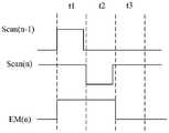
图5示出了图2这种像素驱动电路的第一驱动时序示意图;FIG. 5 shows a schematic diagram of a first driving timing sequence of the pixel driving circuit of FIG. 2;
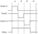
图6示出了图2这种像素驱动电路的第二驱动时序示意图;FIG. 6 shows a second driving timing diagram of the pixel driving circuit of FIG. 2;
图7为本申请实施例中第二种像素驱动电路的组成结构示意图;FIG. 7 is a schematic diagram of the composition and structure of a second pixel driving circuit in an embodiment of the present application;
图8为本申请实施例中第三种像素驱动电路的组成结构示意图;FIG. 8 is a schematic diagram of the composition and structure of a third pixel driving circuit in an embodiment of the present application;
图9为本申请实施例中第四种像素驱动电路的组成结构示意图。FIG. 9 is a schematic diagram of the composition and structure of a fourth pixel driving circuit according to an embodiment of the present application.
具体实施方式Detailed ways
为了能够更加详尽地了解本申请实施例的特点与技术内容,下面结合附图对本申请实施例的实现进行详细阐述,所附附图仅供参考说明之用,并非用来限定本申请实施例。In order to have a more detailed understanding of the features and technical contents of the embodiments of the present application, the implementation of the embodiments of the present application will be described in detail below with reference to the accompanying drawings.
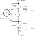
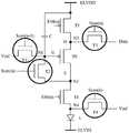
本申请实施例提供了一种像素驱动电路,图1为本申请实施例中一种像素驱动电路的原理结构示意图,如图1所示,所述像素驱动电路包括:初始化模块11、写入模块12、驱动晶体管13和发光模块14;An embodiment of the present application provides a pixel driving circuit. FIG. 1 is a schematic structural diagram of a pixel driving circuit in an embodiment of the present application. As shown in FIG. 1 , the pixel driving circuit includes an
这里,所述初始化模块11用于在初始化阶段对所述驱动晶体管13进行初始化;Here, the
写入模块12用于在数据写入阶段将所述数据信号写入所述驱动晶体管13的控制极;The
驱动晶体管13用于在发光阶段向所述发光模块14提供驱动电流,以驱动所述发光模块14发光。The
图2为本申请实施例中第一种像素驱动电路的组成结构示意图,如图2所示,FIG. 2 is a schematic diagram of the composition and structure of the first pixel driving circuit in the embodiment of the application, as shown in FIG. 2 ,
所述初始化模块11可以包括:第一晶体管T1,所述第一晶体管T1的第一极和所述驱动晶体管T0的控制极在第一节点N1电连接,所述第一晶体管T1的第二极用于接收复位信号Vref,所述初始化模块用于在初始化阶段将所述复位信号Vref传输至所述第一节点N1,对所述驱动晶体T0管进行初始化;The
所述写入模块12包括:第二晶体管T2和第三晶体管T3;所述第二晶体管T2的第一极连接所述第一节点N1,所述第二晶体管T2的第二极和所述驱动晶体管T0的第一极在第二节点N2电连接;所述第三晶体管T3的第一极和所述驱动晶体管T0的第二极在第三节点N3电连接,所述第三晶体管T3的第二极用于接收数据信号Data;所述写入模块用于在数据写入阶段将所述数据信号Data写入到所述第一节点N1;其中,所述第一晶体管T1和所述第二晶体管T2中至少一个为N型薄膜晶体管;The
所述驱动晶体管T0的第二极与所述发光模块的正极相连,用于在发光阶段向所述发光模块提供驱动电流,以驱动所述发光模块发光。The second pole of the driving transistor T0 is connected to the positive pole of the light-emitting module, and is used for providing a driving current to the light-emitting module in the light-emitting stage, so as to drive the light-emitting module to emit light.
这里,发光模块为发光二极管L,驱动晶体管用于驱动发光二极管发光。复位信号Vref是能够始终保持恒定的一个电压,其大小根据实际需求而定。Here, the light-emitting module is a light-emitting diode L, and the driving transistor is used to drive the light-emitting diode to emit light. The reset signal Vref is a voltage that can be kept constant all the time, and its magnitude is determined according to actual requirements.
需要说明的是,所述第一晶体管T1和所述第二晶体管T2中至少一个为N型TFT;其他晶体管(包括驱动晶体管、第三晶体管、第四晶体管、第五晶体管和第六晶体管)可以为N型TFT或者P型TFT。It should be noted that at least one of the first transistor T1 and the second transistor T2 is an N-type TFT; other transistors (including the driving transistor, the third transistor, the fourth transistor, the fifth transistor and the sixth transistor) can be It is an N-type TFT or a P-type TFT.
图2中示出的像素驱动电路,第一晶体管为N型TFT,其他晶体管为P型TFT。In the pixel driving circuit shown in FIG. 2 , the first transistor is an N-type TFT, and the other transistors are P-type TFTs.
需要说明的是,本申请实施例中晶体管的第一极和第二极是用来指示晶体管两极(即漏极和源极),第一极和第二极只是为了表示晶体管的连接关系,第一极并不是表示固定一极,第二极也不是表示固定一极,根据晶体管的类型和在电路中的具体位置第一极和第二极可以灵活表示晶体管的源极和漏极。It should be noted that the first pole and the second pole of the transistor in the embodiments of the present application are used to indicate the two poles of the transistor (ie the drain and the source), and the first pole and the second pole are only used to indicate the connection relationship of the transistor. One pole does not mean a fixed pole, and the second pole does not mean a fixed pole. According to the type of the transistor and the specific position in the circuit, the first pole and the second pole can flexibly represent the source and drain of the transistor.
比如,图2中,第一晶体管T1为N型TFT,T1的第一极表示T1的源极,T1的第二极表示T1的漏极,第二晶体管T2为P型TFT,T2的第一极表示T2的漏极,T2的第二极表示T2的源极,驱动晶体管T0为P型TFT,T0的第一极表示T0的源极,T0的第二极表示T0的漏极。For example, in FIG. 2, the first transistor T1 is an N-type TFT, the first pole of T1 represents the source of T1, the second pole of T1 represents the drain of T1, the second transistor T2 is a P-type TFT, and the first pole of T2 The pole represents the drain of T2, the second pole of T2 represents the source of T2, the driving transistor T0 is a P-type TFT, the first pole of T0 represents the source of T0, and the second pole of T0 represents the drain of T0.
在一些实施例中,N型TFT为铟镓锌氧化物(Indium Gallium Zinc Oxide,IGZO)薄膜晶体管,简称IGZO TFT,P型TFT为低温多晶硅(Low Temperature Poly-Silicon,LTPS)薄膜晶体管,简称LTPS TFT。In some embodiments, the N-type TFT is an Indium Gallium Zinc Oxide (IGZO) thin film transistor, IGZO TFT for short, and the P-type TFT is a Low Temperature Poly-Silicon (LTPS) thin film transistor, LTPS for short TFT.
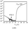
图3为IGZO薄膜晶体管的漏电流示意图,图4为LTPS薄膜晶体管的漏电流示意图,比较图3和图4可以看出IGZO的漏电流比LTPS低两个数量级,IGZO的漏电流比LTPS下降了100倍,根据公式It=cu,I为漏电流,t为保持时间,c为存储电容,u为变化电压,当显示屏的刷新频率由60HZ变为1HZ,保持时间增加了60倍,但是漏电电流下降了100倍,整体来说用IGZO时,电压变化反而减小了。所以T1用IGZO,可以让显示屏的刷新频率下降100倍,也不会出现显示异常,通过降低频率节约功耗。Figure 3 is a schematic diagram of the leakage current of the IGZO thin film transistor, and Figure 4 is a schematic diagram of the leakage current of the LTPS thin film transistor. Comparing Figure 3 and Figure 4, it can be seen that the leakage current of IGZO is two orders of magnitude lower than that of LTPS, and the leakage current of IGZO is lower than that of LTPS. 100 times, according to the formula It=cu, I is the leakage current, t is the holding time, c is the storage capacitor, and u is the changing voltage. When the refresh frequency of the display screen changes from 60HZ to 1HZ, the holding time increases by 60 times, but the leakage current The current dropped by a factor of 100, and overall the voltage change was reduced with IGZO. Therefore, using IGZO for T1 can reduce the refresh frequency of the display screen by 100 times, and there will be no abnormal display, and power consumption can be saved by reducing the frequency.
在一些实施例中,所述像素驱动电路还包括:第四晶体管T4(如图2所示)和发光控制模块15(如图1所示)。In some embodiments, the pixel driving circuit further includes: a fourth transistor T4 (as shown in FIG. 2 ) and a light emission control module 15 (as shown in FIG. 1 ).
需要说明的是,第四晶体管用于在发光阶段之前将所述复位信号传输至所述发光模块的正极,对所述发光模块进行复位。发光阶段之前可以为初始化阶段、写入阶段、或者写入阶段和初始化阶段之间的阶段。It should be noted that the fourth transistor is used to transmit the reset signal to the positive electrode of the light-emitting module before the light-emitting stage, so as to reset the light-emitting module. The light-emitting phase may be preceded by an initialization phase, a writing phase, or a phase between the writing phase and the initialization phase.
发光控制模块15用于控制驱动电流通入到发光模块14,以驱动发光模块14发光。The
具体电路图如图2所示,所述第四晶体管T4的第一极与所述发光模块(即发光二极管L)的正极在第四节点N4电连接,所述第四晶体管的第二极用于接收复位信号Vref;所述第四晶体管T4用于在发光阶段之前将所述复位信号传输至发光二极管L的正极,对发光二极管L进行复位;The specific circuit diagram is shown in FIG. 2 , the first pole of the fourth transistor T4 is electrically connected to the anode of the light-emitting module (ie, the light-emitting diode L) at the fourth node N4, and the second pole of the fourth transistor is used for receiving a reset signal Vref; the fourth transistor T4 is used to transmit the reset signal to the anode of the light-emitting diode L before the light-emitting stage, so as to reset the light-emitting diode L;
所述发光控制模块15可以包括:第五晶体管T5和第六晶体管T6;The
所述第五晶体管T5的第一极连接第一电压信号端ELVDD,所述第五晶体管T5的第二极连接所述第三节点N3;The first pole of the fifth transistor T5 is connected to the first voltage signal terminal ELVDD, and the second pole of the fifth transistor T5 is connected to the third node N3;
所述第六晶体管T6的第一极连接所述第二节点N2,所述第六晶体管的第二极连接所述第四节点N4;The first pole of the sixth transistor T6 is connected to the second node N2, and the second pole of the sixth transistor is connected to the fourth node N4;
发光二极管L的负极连接第二电压信号端ELVSS。The cathode of the light emitting diode L is connected to the second voltage signal terminal ELVSS.
在一些实施例中,所述像素驱动电路还包括:存储电容;存储电容用于存储写入数据的电信号。In some embodiments, the pixel driving circuit further includes: a storage capacitor; the storage capacitor is used to store the electrical signal of the written data.
如图2所示,所述存储电容C的第一端连接所述第一电压信号端ELVDD,所述存储电容C的第二端连接所述第一节点N1;所述存储电容C用于在初始化阶段利用所述复位信号Vref进行充电,并利用充电电压对所述驱动晶体管T0进行初始化;在数据写入阶段保存所述数据信号Data;在发光阶段驱动所述驱动晶体管T0产生驱动电流。As shown in FIG. 2 , the first terminal of the storage capacitor C is connected to the first voltage signal terminal ELVDD, and the second terminal of the storage capacitor C is connected to the first node N1; the storage capacitor C is used for In the initialization stage, the reset signal Vref is used for charging, and the charging voltage is used to initialize the driving transistor T0; the data signal Data is saved in the data writing stage; and the driving transistor T0 is driven to generate a driving current in the light-emitting stage.
在一些实施例中,所述第二晶体管和第三晶体管为相同类型的薄膜晶体管,比如,同为N型薄膜晶体管,或者同为P型薄膜晶体管。为了减少扫描信号线数量,第四晶体管和第一晶体管为相同类型的薄膜晶体管,可以公共一根扫描线,或者第四晶体管、第二晶体管和第三晶体管为相同类型的薄膜晶体管,可以公共一根扫描线。In some embodiments, the second transistor and the third transistor are the same type of thin film transistor, for example, both are N-type thin film transistors, or both are P-type thin film transistors. In order to reduce the number of scan signal lines, the fourth transistor and the first transistor are thin film transistors of the same type, and can share one scan line, or the fourth transistor, the second transistor, and the third transistor are thin film transistors of the same type, and can share one root scan line.
实际应用中,像素驱动电路中晶体管还需接入控制信号,以控制晶体管导通或截止,从而实现像素单元正常工作,不同类型的薄膜晶体管需要占用不同的走线。In practical applications, the transistor in the pixel driving circuit also needs to be connected to a control signal to control the transistor to be turned on or off, so as to realize the normal operation of the pixel unit, and different types of thin film transistors need to occupy different wirings.
具体地,所述第一晶体管的控制极接入第一扫描信号;Specifically, the control electrode of the first transistor is connected to the first scan signal;
所述第二晶体管的控制极和第三晶体管的控制极接入第二扫描信号;The control electrode of the second transistor and the control electrode of the third transistor are connected to the second scan signal;
所述第五晶体管的控制极和所述第六晶体管的控制极接入发光控制信号;The control electrode of the fifth transistor and the control electrode of the sixth transistor are connected to a light-emitting control signal;
其中,所述第一扫描信号、所述第二扫描信号和所述发光控制信号为不同时序信号。Wherein, the first scan signal, the second scan signal and the light emission control signal are signals of different timings.
需要说明的是,在初始化阶段由第一扫描信号控制第一晶体管导通,在写入阶段由第二扫描信号控制第二晶体管和第三晶体管导通,在写入阶段由发光控制信号控制五晶体管和第六晶体管导通。因此,第一扫描信号的有效电平早于第二扫描信号的有效电平,第二扫描信号的有效电平早于发光控制信号的有效电平。It should be noted that in the initialization stage, the first transistor is controlled to be turned on by the first scan signal, the second transistor and the third transistor are controlled to be turned on by the second scan signal in the writing stage, and the light-emitting control signal is controlled by the light-emitting control signal in the writing stage. The transistor and the sixth transistor are turned on. Therefore, the active level of the first scan signal is earlier than the active level of the second scan signal, and the active level of the second scan signal is earlier than the active level of the light emission control signal.
需要说明的是,第一晶体管控制极单独使用一根扫描走线;第二晶体管和第三晶体管的控制极都接第二扫描信号,表明第二晶体管和第三晶体管同时导通,同时截止,所以第二晶体管和第三晶体管为相同类型的薄膜晶体管,第二晶体管和第三晶体管控制极共用一根扫描走线。It should be noted that the control electrode of the first transistor uses a single scan line; the control electrodes of the second transistor and the third transistor are both connected to the second scan signal, indicating that the second transistor and the third transistor are turned on and off at the same time, Therefore, the second transistor and the third transistor are thin film transistors of the same type, and the control electrodes of the second transistor and the third transistor share one scan line.
同样,第五晶体管和第六晶体管的控制极都接发光控制信号,表明第五晶体管和第六晶体管同时导通,同时截止,所以第五晶体管和第六晶体管为相同类型的薄膜晶体管,第五晶体管和第六晶体管控制极共用一根控制走线。Similarly, the control electrodes of the fifth transistor and the sixth transistor are both connected to the light-emitting control signal, indicating that the fifth transistor and the sixth transistor are turned on and off at the same time, so the fifth transistor and the sixth transistor are the same type of thin film transistors, the fifth transistor The transistor and the control electrode of the sixth transistor share a control line.
图5示出了图2这种像素驱动电路的第一驱动时序示意图,如图5所示,在初始化阶段t1第一扫描信号Scan(n-1)高电平有效,控制T1导通,其他晶体管截止,将Vref输入到存储电容C的N1端,使存储电容复位;FIG. 5 shows a schematic diagram of the first driving timing of the pixel driving circuit of FIG. 2. As shown in FIG. 5, in the initialization stage t1, the first scan signal Scan(n-1) is active at a high level, and control T1 to conduct, and other The transistor is turned off, and Vref is input to the N1 terminal of the storage capacitor C to reset the storage capacitor;
在写入阶段t2第二扫描信号Scan(n)低电平有效,控制T2和T3导通,其他晶体管截止,将Data写入到存储电容C;In the writing phase t2, the second scan signal Scan(n) is active at low level, controls T2 and T3 to be turned on, and other transistors are turned off to write Data into the storage capacitor C;
在发光阶段t3发光控制信号EM(n)低电平有效,控制T5和T6导通,存储电容C放电,以使得驱动晶体管在驱动电流的作用下导通,驱动电流流经T6驱动发光二极管L发光。In the light-emitting stage t3, the light-emitting control signal EM(n) is active at low level, controls T5 and T6 to be turned on, and the storage capacitor C is discharged, so that the driving transistor is turned on under the action of the driving current, and the driving current flows through T6 to drive the light-emitting diode L. glow.
在一些实施例中,所述第四晶体管的控制极接入所述第一扫描信号、所述第二扫描信号或第三扫描信号;其中,所述第一扫描信号、所述第二扫描信号、所述第三扫描信号和所述发光控制信号为不同时序信号。In some embodiments, the control electrode of the fourth transistor is connected to the first scan signal, the second scan signal or the third scan signal; wherein the first scan signal and the second scan signal , the third scan signal and the light-emitting control signal are different timing signals.
需要说明的是,为了减少走线数量,第四晶体管与第一晶体管为相同类型的薄膜晶体管,共用一根扫描走线,即发光二极管在初始化阶段复位;第四晶体管也可以与第二晶体管为相同类型的薄膜晶体管,共用一根扫描走线,即发光二极管在写入阶段复位。或者在写入阶段之后复位,第四晶体管单独占用一根扫描走线,通过第三扫描信号Scan(n+1)控制T4导通,从而使发光二极管复位。It should be noted that, in order to reduce the number of lines, the fourth transistor and the first transistor are thin film transistors of the same type and share a scan line, that is, the light emitting diode is reset during the initialization stage; the fourth transistor and the second transistor can also be Thin film transistors of the same type share one scan line, that is, the light-emitting diodes are reset during the writing phase. Or reset after the writing stage, the fourth transistor occupies a scan line alone, and the third scan signal Scan(n+1) controls T4 to be turned on, so that the light-emitting diode is reset.
图6示出了图2这种像素驱动电路的第二驱动时序示意图,图6中增加了第三扫描信号Scan(n+1)。FIG. 6 shows a second driving timing diagram of the pixel driving circuit of FIG. 2 , and a third scan signal Scan(n+1) is added in FIG. 6 .
在初始化阶段t1第一扫描信号Scan(n-1)高电平有效,控制T1导通,其他晶体管截止,将Vref输入到存储电容C的N1端,使存储电容复位;In the initialization stage t1, the first scan signal Scan(n-1) is active at high level, control T1 to be turned on, other transistors are turned off, and Vref is input to the N1 end of the storage capacitor C to reset the storage capacitor;
在写入阶段t2第二扫描信号Scan(n)低电平有效,控制T2和T3导通,其他晶体管截止,将Data写入到存储电容C;In the writing phase t2, the second scan signal Scan(n) is active at low level, controls T2 and T3 to be turned on, and other transistors are turned off to write Data into the storage capacitor C;
在发光二极管复位阶段t3第三扫描信号Scan(n+1)低电平有效,控制T4导通,其他晶体管截止,复位信号Vref使发光二极管复位;In the light-emitting diode reset stage t3, the third scan signal Scan(n+1) is active at low level, controls T4 to be turned on, other transistors are turned off, and the reset signal Vref resets the light-emitting diode;
在发光阶段t4发光控制信号EM(n)低电平有效,控制T5和T6导通,存储电容C放电,以使得驱动晶体管在驱动电流的作用下导通,驱动电流流经T6驱动发光二极管L发光。In the light-emitting stage t4, the light-emitting control signal EM(n) is active at low level, controls T5 and T6 to be turned on, and the storage capacitor C is discharged, so that the driving transistor is turned on under the action of the driving current, and the driving current flows through T6 to drive the light-emitting diode L. glow.
图7为本申请实施例中第二种像素驱动电路的组成结构示意图,如图7所示,第二晶体管T2为N型TFT,为了减少走线数量第三晶体管T3也为N型TFT,若发光二极管L在写入阶段被复位,则第四晶体管T4也可以为N型TFT,与T2和T3共用一根走线。FIG. 7 is a schematic diagram of the composition structure of the second pixel driving circuit in the embodiment of the present application. As shown in FIG. 7 , the second transistor T2 is an N-type TFT, and the third transistor T3 is also an N-type TFT in order to reduce the number of wirings. The light emitting diode L is reset in the writing stage, and the fourth transistor T4 can also be an N-type TFT, which shares a wiring with T2 and T3.
需要说明的是,若发光二极管L在初始化阶段被复位,第四晶体管T4可以为P型TFT,扫描信号为S(n-1),与T1共用一根扫描走线。It should be noted that, if the light emitting diode L is reset in the initialization stage, the fourth transistor T4 can be a P-type TFT, the scanning signal is S(n-1), and a scanning line is shared with T1.
还需要说明的是,若发光二极管L在写入阶段之后复位,第四晶体管单独占用一根扫描走线,通过第三扫描信号Scan(n+1)控制T4导通,从而使发光二极管复位,此时T4可以为N型TFT,也可以为P型TFT。It should also be noted that, if the light-emitting diode L is reset after the writing stage, the fourth transistor occupies a single scan line, and the third scan signal Scan(n+1) controls T4 to be turned on, so that the light-emitting diode is reset, At this time, T4 may be an N-type TFT or a P-type TFT.
这里,S(n-1)的有效信号早于S(n),S(n)的有效信号早于S(n+1),S(n+1)早于EM(n)。Here, the valid signal of S(n-1) is earlier than S(n), the valid signal of S(n) is earlier than S(n+1), and S(n+1) is earlier than EM(n).
图8为本申请实施例中第三种像素驱动电路的组成结构示意图,如图8所示,第一晶体管T1和第二晶体管T2均为N型TFT,为了减少走线数量第三晶体管T3也为N型TFT,同样若发光二极管L在写入阶段被复位,则第四晶体管T4也可以为N型TFT,扫描信号为S(n),与T2和T3共用一根扫描走线。FIG. 8 is a schematic diagram of the composition and structure of a third pixel driving circuit in an embodiment of the present application. As shown in FIG. 8 , the first transistor T1 and the second transistor T2 are both N-type TFTs. In order to reduce the number of wirings, the third transistor T3 is also It is an N-type TFT. Similarly, if the light-emitting diode L is reset during the writing phase, the fourth transistor T4 can also be an N-type TFT, and the scan signal is S(n), which shares a scan line with T2 and T3.
需要说明的是,若发光二极管L在初始化阶段被复位,第四晶体管T4也可以为N型TFT,扫描信号为S(n-1),与T1共用一根扫描走线。It should be noted that, if the light-emitting diode L is reset in the initialization stage, the fourth transistor T4 can also be an N-type TFT, the scanning signal is S(n-1), and a scanning line is shared with T1.
还需要说明的是,若发光二极管L在写入阶段之后复位,第四晶体管单独占用一根扫描走线,通过第三扫描信号Scan(n+1)控制T4导通,从而使发光二极管复位,此时T4可以为N型TFT,也可以为P型TFT。It should also be noted that, if the light-emitting diode L is reset after the writing stage, the fourth transistor occupies a single scan line, and the third scan signal Scan(n+1) controls T4 to be turned on, so that the light-emitting diode is reset, At this time, T4 may be an N-type TFT or a P-type TFT.
采用本申请实施例提供的像素驱动电路,在驱动晶体管的控制极电压受到与之连接的第一晶体管和第二晶体管的漏电流影响的情况下,由于N型薄膜晶体管的漏电流较小,第一晶体管使用N型薄膜晶体,和/或第二晶体管中使用N型薄膜晶体管,能够较大程度减小驱动晶体管控制极的漏电流,从而减小控制极电压变化,解决了发光模块显示异常的问题。With the pixel driving circuit provided in the embodiment of the present application, when the gate voltage of the driving transistor is affected by the leakage current of the first transistor and the second transistor connected to it, the leakage current of the N-type thin film transistor is small, and the Using an N-type thin film transistor in one transistor, and/or using an N-type thin film transistor in the second transistor, can greatly reduce the leakage current of the control electrode of the driving transistor, thereby reducing the voltage change of the control electrode, and solving the problem of abnormal display of the light-emitting module. question.
在上述实施例的基础上,本申请实施例还给出了另一种像素补偿电路,图9为本申请实施例中第四种像素驱动电路的组成结构示意图,如图9所示,On the basis of the above-mentioned embodiment, the embodiment of the present application also provides another pixel compensation circuit. FIG. 9 is a schematic diagram of the composition and structure of the fourth pixel driving circuit in the embodiment of the present application, as shown in FIG. 9 ,
所述初始化模块11可以包括:第一晶体管T1,所述第一晶体管T1的第一极和所述驱动晶体管T0的控制极在第一节点N1电连接,所述第一晶体管T1的第二极用于接收复位信号Vref,所述初始化模块用于在初始化阶段将所述复位信号Vref传输至所述第一节点N1,对所述驱动晶体T0管进行初始化;The
所述写入模块12包括:第二晶体管T2和第三晶体管T3;所述第二晶体管T2的第一极连接所述第一节点N1,所述第二晶体管T2的第二极和所述驱动晶体管T0的第一极在第二节点N2电连接;所述第三晶体管T3的第一极和所述驱动晶体管T0的第二极在第三节点N3电连接,所述第三晶体管T3的第二极用于接收数据信号Data;所述写入模块用于在数据写入阶段将所述数据信号Data写入到所述第一节点N1;其中,所述第一晶体管T1和所述第二晶体管T2中至少一个为N型薄膜晶体管;The
所述驱动晶体管T0的第二极与所述发光模块的正极相连,用于在发光阶段向所述发光模块提供驱动电流,以驱动所述发光模块发光。The second pole of the driving transistor T0 is connected to the positive pole of the light-emitting module, and is used for providing a driving current to the light-emitting module in the light-emitting stage, so as to drive the light-emitting module to emit light.
所述第四晶体管T4的第一极与所述发光模块(即发光二极管L)的正极在第四节点N4电连接,所述第四晶体管的第二极用于接收复位信号Vref;所述第四晶体管T4用于在发光阶段之前将所述复位信号传输至发光二极管L的正极,对发光二极管L进行复位;The first pole of the fourth transistor T4 is electrically connected to the anode of the light-emitting module (ie, the light-emitting diode L) at the fourth node N4, and the second pole of the fourth transistor is used to receive the reset signal Vref; The four transistors T4 are used to transmit the reset signal to the anode of the light-emitting diode L before the light-emitting stage, so as to reset the light-emitting diode L;
所述发光控制模块15可以包括:第五晶体管T5和第六晶体管T6;The
所述第五晶体管T5的第一极连接第一电压信号端ELVDD,所述第五晶体管T5的第二极连接所述第三节点N3;所述第六晶体管T6的第一极连接所述第二节点N2,所述第六晶体管的第二极连接所述第四节点N4;发光二极管L的负极连接第二电压信号端ELVSS。The first electrode of the fifth transistor T5 is connected to the first voltage signal terminal ELVDD, the second electrode of the fifth transistor T5 is connected to the third node N3, and the first electrode of the sixth transistor T6 is connected to the third node N3. Two nodes N2, the second pole of the sixth transistor is connected to the fourth node N4; the cathode of the light emitting diode L is connected to the second voltage signal terminal ELVSS.
存储电容C的第一端连接所述第一电压信号端ELVDD,所述存储电容C的第二端连接所述第一节点N1;所述存储电容C用于在初始化阶段利用所述复位信号Vref进行充电,并利用充电电压对所述驱动晶体管T0进行初始化;在数据写入阶段保存所述数据信号Data;在发光阶段驱动所述驱动晶体管T0产生驱动电流。The first terminal of the storage capacitor C is connected to the first voltage signal terminal ELVDD, and the second terminal of the storage capacitor C is connected to the first node N1; the storage capacitor C is used to use the reset signal Vref in the initialization stage Perform charging, and initialize the driving transistor T0 with a charging voltage; save the data signal Data in the data writing stage; drive the driving transistor T0 to generate a driving current in the light-emitting stage.
所述第一晶体管T1为N型薄膜晶体管时所述初始化模块还包括第一辅晶体管T11,所述第二晶体管T2为N型薄膜晶体管时所述写入模块还包括第二辅晶体管T21;所述第一辅晶体管T11和所述第二辅晶体管T21为P型薄膜晶体管;When the first transistor T1 is an N-type thin film transistor, the initialization module further includes a first auxiliary transistor T11, and when the second transistor T2 is an N-type thin film transistor, the writing module further includes a second auxiliary transistor T21; The first auxiliary transistor T11 and the second auxiliary transistor T21 are P-type thin film transistors;
所述第一辅晶体管T11的第一极连接所述第一晶体管T1的第二极,所述第一辅晶体管T11的第二极接收复位信号Vref;The first pole of the first auxiliary transistor T11 is connected to the second pole of the first transistor T1, and the second pole of the first auxiliary transistor T11 receives the reset signal Vref;
所述第二辅晶体管T21的第一极连接所述第二晶体管T2的第二极,所述第二辅晶体管T21的第二极连接所述第二节点N2。The first pole of the second auxiliary transistor T21 is connected to the second pole of the second transistor T2, and the second pole of the second auxiliary transistor T21 is connected to the second node N2.
需要说明的是,本申请实施例中晶体管(包括辅晶体管)的第一极和第二极是用来指示晶体管两极(即漏极和源极),第一极和第二极只是为了表示晶体管的连接关系,第一极并不是表示固定一极,第二极也不是表示固定一极,根据晶体管的类型和在电路中的具体位置第一极和第二极可以灵活表示晶体管的源极和漏极。It should be noted that the first and second poles of the transistor (including the auxiliary transistor) in the embodiments of the present application are used to indicate the two poles of the transistor (ie the drain and the source), and the first and second poles are only used to indicate the transistor The connection relationship, the first pole does not mean a fixed pole, and the second pole does not mean a fixed pole. According to the type of the transistor and the specific position in the circuit, the first pole and the second pole can flexibly represent the source and drain.
需要说明的是,图9示出了T1和T2同时为N型TFT时的一种像素驱动电路,若只有T1为N型TFT,则像素驱动电路中可以只包括T11,若只有T2为N型TFT,则像素驱动电路中可以只包括T21。It should be noted that FIG. 9 shows a pixel driving circuit when T1 and T2 are both N-type TFTs. If only T1 is an N-type TFT, only T11 may be included in the pixel driving circuit. If only T2 is an N-type TFT TFT, then only T21 can be included in the pixel driving circuit.
在一些实施例中,若T1为P型TFT,则初始化模块也可以包括T11,此时T11为N型TFT,若T2为P型TFT,则写入模块也可以包括T21,此时T21为N型TFT。In some embodiments, if T1 is a P-type TFT, the initialization module may also include T11, and T11 is an N-type TFT. If T2 is a P-type TFT, the writing module may also include T21, and T21 is N at this time. type TFT.
需要说明的是,由于N型TFT的漏电流比P型TFT低两个数量级,且T0控制极主要收到T1和T2漏电流的影响,因此,只要与第一节点N1连接的初始化模块中包含N型TFT,和/或,与第一节点N1连接的写入模块中包含N型TFT,则便可以达到减小漏电流的目的,至于初始化模块中是否还串联P型TFT则无关紧要,写入模块中是否还串联也P型TFT则无关紧要。It should be noted that since the leakage current of N-type TFT is two orders of magnitude lower than that of P-type TFT, and the T0 gate is mainly affected by the leakage currents of T1 and T2, as long as the initialization module connected to the first node N1 contains N-type TFT, and/or, if the writing module connected to the first node N1 includes N-type TFT, the purpose of reducing leakage current can be achieved. It does not matter whether a P-type TFT is connected in series in the initialization module. It does not matter whether the P-type TFT is also connected in series in the module.
实际应用中,像素驱动电路中晶体管还需接入控制信号,以控制晶体管导通或截止,从而实现像素单元正常工作。In practical applications, the transistor in the pixel driving circuit also needs to be connected to a control signal to control the transistor to be turned on or off, so as to realize the normal operation of the pixel unit.
在一些实施例中,所述第一晶体管的控制极接入第一扫描信号,所述第一辅晶体管的控制极接入第一辅扫描信号;In some embodiments, the control electrode of the first transistor is connected to the first scan signal, and the control electrode of the first auxiliary transistor is connected to the first auxiliary scan signal;
所述第二晶体管的控制极和第三晶体管的控制极接入第二扫描信号,所述第二辅晶体管的控制极接入第二辅扫描信号;The control electrode of the second transistor and the control electrode of the third transistor are connected to the second scanning signal, and the control electrode of the second auxiliary transistor is connected to the second auxiliary scanning signal;
所述第五晶体管的控制极和所述第六晶体管的控制极接入发光控制信号;The control electrode of the fifth transistor and the control electrode of the sixth transistor are connected to a light-emitting control signal;
其中,所述第一扫描信号、所述第二扫描信号和所述发光控制信号为不同时序信号,所述第一扫描信号和所述第一辅扫描信号的有效电平相反,所述第二扫描信号和所述第二辅扫描信号的有效电平相反。The first scan signal, the second scan signal, and the light-emitting control signal are different timing signals, the first scan signal and the first auxiliary scan signal have opposite effective levels, and the second scan signal has opposite effective levels. The active levels of the scan signal and the second auxiliary scan signal are opposite.
需要说明的是,如果T1和T11为不同类型的TFT,则为了使T1和T11在初始化阶段同时导通,就需要T11控制极单独使用一根扫描走线,来接入第一辅扫描信号Scan(n-1),T1单独使用一根扫描走线,来接入第一扫描信号Scan(n-1)1。比如,T1为N型TFT,第一扫描信号低电平有效,T11为P型TFT,第一辅扫描信号高电平有效。It should be noted that if T1 and T11 are different types of TFTs, in order to make T1 and T11 turn on at the same time in the initialization stage, it is necessary to use a single scan line for the control electrode of T11 to access the first auxiliary scan signal Scan (n-1), T1 uses a single scan line to access the first scan signal Scan(n-1)1. For example, T1 is an N-type TFT, and the first scan signal is active at a low level, and T11 is a P-type TFT, and the first auxiliary scan signal is active at a high level.
如果T2和T21为不同类型的TFT,则为了使T2和T21在写入阶段同时导通,就需要T21控制极单独使用一根扫描走线,来接入第二辅扫描信号Scan(n),T2单独使用一根扫描走线,来接入第二扫描信号Scan(n)1。比如,T2为N型TFT,第二扫描信号低电平有效,T21为P型TFT,第二辅扫描信号高电平有效。If T2 and T21 are different types of TFTs, in order to make T2 and T21 turn on at the same time during the writing stage, it is necessary to use a separate scan line for the control electrode of T21 to access the second auxiliary scan signal Scan(n), T2 uses a scan line alone to access the second scan signal Scan(n)1. For example, T2 is an N-type TFT, and the second scan signal is active at a low level, and T21 is a P-type TFT, and the second auxiliary scan signal is active at a high level.
采用本申请实施例提供的像素驱动电路,在驱动晶体管的控制极电压受到与之连接的第一晶体管和第二晶体管的漏电流影响的情况下,由于N型薄膜晶体管的漏电流较小,第一晶体管使用N型薄膜晶体,和/或第二晶体管中使用N型薄膜晶体管,能够较大程度减小驱动晶体管控制极的漏电流,从而减小控制极电压变化,解决了发光模块显示异常的问题。With the pixel driving circuit provided in the embodiment of the present application, when the gate voltage of the driving transistor is affected by the leakage current of the first transistor and the second transistor connected to it, the leakage current of the N-type thin film transistor is small, and the Using an N-type thin film transistor in one transistor, and/or using an N-type thin film transistor in the second transistor, can greatly reduce the leakage current of the control electrode of the driving transistor, thereby reducing the voltage change of the control electrode, and solving the problem of abnormal display of the light-emitting module. question.
基于上述实施方式,本申请实施例中还提供了一种显示面板包括像素阵列,其中,像素阵列中每个像素包括上述实施例中任一种像素驱动电路。Based on the foregoing implementation manner, an embodiment of the present application further provides a display panel including a pixel array, wherein each pixel in the pixel array includes any one of the pixel driving circuits in the foregoing embodiments.
包含本申请实施例上述像素驱动电路的显示面板,具备较高的显示质量,不会存在因晶体管漏电流影响导致的显示异常的问题。The display panel including the pixel driving circuit of the embodiment of the present application has high display quality, and there is no problem of abnormal display caused by the leakage current of the transistor.
基于上述显示面板,本申请实施例中还提供了一种电子设备,该电子设备包括上述任一种显示面板。Based on the above-mentioned display panel, an electronic device is also provided in the embodiments of the present application, and the electronic device includes any of the above-mentioned display panels.
本申请实施例所记载的技术方案之间,在不冲突的情况下,可以任意组合。The technical solutions described in the embodiments of the present application may be combined arbitrarily if there is no conflict.
在本申请所提供的几个实施例中,应该理解到,所揭露的驱动晶体管、初始化模块、写入模块、发光控制模块和发光模块的实施例仅仅是示意性的介绍了本申请像素驱动电路的实现原理,并不是限定实际的实现电路,实际电路还可以通过其它的方式实现。在本申请以上基本原理的基础上所实现温度检测电路都应涵盖在本申请的保护范围之内。In the several embodiments provided in the present application, it should be understood that the disclosed embodiments of the driving transistor, the initialization module, the writing module, the light-emitting control module and the light-emitting module are only a schematic introduction to the pixel driving circuit of the present application The realization principle does not limit the actual realization circuit, and the actual circuit can also be realized in other ways. The temperature detection circuit implemented on the basis of the above basic principles of the present application should all be covered by the protection scope of the present application.
以上所述,仅为本申请的具体实施方式,但本申请的保护范围并不局限于此,任何熟悉本技术领域的技术人员在本申请揭露的技术范围内,可轻易想到变化或替换,都应涵盖在本申请的保护范围之内。The above are only specific embodiments of the present application, but the protection scope of the present application is not limited to this. should be covered within the scope of protection of this application.
Claims (8)
Priority Applications (1)
| Application Number | Priority Date | Filing Date | Title |
|---|---|---|---|
| CN202011080105.4ACN112233621B (en) | 2020-10-10 | 2020-10-10 | A pixel drive circuit, a display panel and an electronic device |
Applications Claiming Priority (1)
| Application Number | Priority Date | Filing Date | Title |
|---|---|---|---|
| CN202011080105.4ACN112233621B (en) | 2020-10-10 | 2020-10-10 | A pixel drive circuit, a display panel and an electronic device |
Publications (2)
| Publication Number | Publication Date |
|---|---|
| CN112233621A CN112233621A (en) | 2021-01-15 |
| CN112233621Btrue CN112233621B (en) | 2022-10-18 |
Family
ID=74113201
Family Applications (1)
| Application Number | Title | Priority Date | Filing Date |
|---|---|---|---|
| CN202011080105.4AActiveCN112233621B (en) | 2020-10-10 | 2020-10-10 | A pixel drive circuit, a display panel and an electronic device |
Country Status (1)
| Country | Link |
|---|---|
| CN (1) | CN112233621B (en) |
Families Citing this family (8)
| Publication number | Priority date | Publication date | Assignee | Title |
|---|---|---|---|---|
| CN113112964B (en)* | 2021-04-14 | 2022-08-09 | 京东方科技集团股份有限公司 | Pixel circuit, pixel driving method and display device |
| GB2615719A (en) | 2021-04-26 | 2023-08-16 | Boe Technology Group Co Ltd | Pixel circuit, pixel driving method and display device |
| US12236855B2 (en) | 2021-05-25 | 2025-02-25 | Chengdu Boe Optoelectronics Technology Co., Ltd. | Pixel circuit, driving method thereof, and display apparatus |
| CN115691399B (en)* | 2021-07-30 | 2024-04-23 | 京东方科技集团股份有限公司 | Display panel and display device |
| CN116524848A (en)* | 2022-01-21 | 2023-08-01 | 成都辰显光电有限公司 | Pixel driving circuit and display panel |
| CN114566127A (en)* | 2022-03-04 | 2022-05-31 | 武汉天马微电子有限公司 | Pixel circuit, driving method thereof and display panel |
| CN114758624B (en)* | 2022-03-31 | 2023-07-04 | 武汉天马微电子有限公司 | Pixel circuit, driving method thereof, array substrate, display panel and display device |
| CN114974097A (en)* | 2022-06-29 | 2022-08-30 | 武汉华星光电半导体显示技术有限公司 | Pixel circuit and display panel |
Citations (2)
| Publication number | Priority date | Publication date | Assignee | Title |
|---|---|---|---|---|
| CN110599964A (en)* | 2019-06-26 | 2019-12-20 | 合肥维信诺科技有限公司 | Pixel driving circuit and display device |
| CN111754922A (en)* | 2020-07-24 | 2020-10-09 | 武汉华星光电半导体显示技术有限公司 | Pixel driving circuit and driving method thereof, and display panel |
Family Cites Families (9)
| Publication number | Priority date | Publication date | Assignee | Title |
|---|---|---|---|---|
| CN107452339B (en)* | 2017-07-31 | 2019-08-09 | 上海天马有机发光显示技术有限公司 | Pixel circuit, driving method thereof, organic light-emitting display panel and display device |
| KR102482575B1 (en)* | 2017-10-31 | 2022-12-28 | 엘지디스플레이 주식회사 | Organic light emitting display device |
| CN107610651B (en)* | 2017-10-31 | 2019-11-08 | 武汉天马微电子有限公司 | Pixel circuit, driving method of pixel circuit and display panel |
| CN107680537B (en)* | 2017-11-21 | 2019-11-29 | 上海天马微电子有限公司 | Driving method of pixel circuit |
| CN110277060B (en)* | 2019-05-21 | 2021-11-16 | 合肥维信诺科技有限公司 | Pixel circuit and display device |
| CN110223640A (en)* | 2019-06-26 | 2019-09-10 | 昆山国显光电有限公司 | A kind of pixel-driving circuit and display device |
| CN111354314A (en)* | 2020-03-16 | 2020-06-30 | 昆山国显光电有限公司 | Pixel circuit, driving method of pixel circuit and display panel |
| CN111613177A (en)* | 2020-06-28 | 2020-09-01 | 上海天马有机发光显示技术有限公司 | Pixel circuit, driving method thereof, display panel and display device |
| CN111754920A (en)* | 2020-07-17 | 2020-10-09 | 武汉华星光电半导体显示技术有限公司 | Pixel driving circuit, driving method thereof and display panel |
- 2020
- 2020-10-10CNCN202011080105.4Apatent/CN112233621B/enactiveActive
Patent Citations (2)
| Publication number | Priority date | Publication date | Assignee | Title |
|---|---|---|---|---|
| CN110599964A (en)* | 2019-06-26 | 2019-12-20 | 合肥维信诺科技有限公司 | Pixel driving circuit and display device |
| CN111754922A (en)* | 2020-07-24 | 2020-10-09 | 武汉华星光电半导体显示技术有限公司 | Pixel driving circuit and driving method thereof, and display panel |
Also Published As
| Publication number | Publication date |
|---|---|
| CN112233621A (en) | 2021-01-15 |
Similar Documents
| Publication | Publication Date | Title |
|---|---|---|
| CN112233621B (en) | A pixel drive circuit, a display panel and an electronic device | |
| US12300172B2 (en) | Pixel circuit and driving method therefor and display panel | |
| US11837162B2 (en) | Pixel circuit and driving method thereof, display panel | |
| US11881164B2 (en) | Pixel circuit and driving method thereof, and display panel | |
| CN110660360B (en) | Pixel circuit and driving method thereof, and display panel | |
| US10978002B2 (en) | Pixel circuit and driving method thereof, and display panel | |
| US20210118361A1 (en) | Amoled pixel driving circuit, driving method, and display panel | |
| WO2021238470A1 (en) | Pixel circuit and driving method thereof and display panel | |
| CN109243369A (en) | Display panel, the driving method of pixel circuit and display device | |
| CN110164375B (en) | Pixel compensation circuit, driving method, electroluminescence display panel and display device | |
| CN107342051A (en) | A kind of image element circuit, display device, pixel circuit drive method | |
| CN108777131B (en) | AMOLED pixel driving circuit and driving method | |
| CN106097964A (en) | Image element circuit, display floater, display device and driving method | |
| CN109979394A (en) | Pixel circuit and its driving method, array substrate and display device | |
| US10424249B2 (en) | Pixel driving circuit and driving method thereof, array substrate, and display device | |
| CN105096826A (en) | Pixel circuit and driving method thereof, array substrate and display device | |
| CN112289269A (en) | Pixel circuit, control method thereof and display panel | |
| CN107393475A (en) | Pixel-driving circuit, image element driving method and display device | |
| CN106971691A (en) | A kind of image element circuit, driving method and display device | |
| CN108172171B (en) | Pixel driving circuit and organic light emitting diode display | |
| CN113096593A (en) | Pixel unit, array substrate and display terminal | |
| CN110992891B (en) | Pixel driving circuit, driving method and display substrate | |
| US11942035B2 (en) | Display panel, method for driving display panel, and display device | |
| CN109308875A (en) | A pixel circuit, a driving method thereof, a display panel and a display device | |
| CN117012153A (en) | Pixel circuit, driving method thereof and display panel |
Legal Events
| Date | Code | Title | Description |
|---|---|---|---|
| PB01 | Publication | ||
| PB01 | Publication | ||
| SE01 | Entry into force of request for substantive examination | ||
| SE01 | Entry into force of request for substantive examination | ||
| GR01 | Patent grant | ||
| GR01 | Patent grant |