CN112197941B - In-situ loss measuring device and method on-chip waveguide - Google Patents
In-situ loss measuring device and method on-chip waveguideDownload PDFInfo
- Publication number
- CN112197941B CN112197941BCN202010978883.9ACN202010978883ACN112197941BCN 112197941 BCN112197941 BCN 112197941BCN 202010978883 ACN202010978883 ACN 202010978883ACN 112197941 BCN112197941 BCN 112197941B
- Authority
- CN
- China
- Prior art keywords
- waveguide
- probe
- chip
- chip waveguide
- light
- Prior art date
- Legal status (The legal status is an assumption and is not a legal conclusion. Google has not performed a legal analysis and makes no representation as to the accuracy of the status listed.)
- Active
Links
- 238000000034methodMethods0.000titleclaimsabstractdescription25
- 238000011065in-situ storageMethods0.000titleclaimsabstractdescription21
- 239000000523sampleSubstances0.000claimsabstractdescription115
- 238000005259measurementMethods0.000claimsabstractdescription45
- 230000003287optical effectEffects0.000claimsabstractdescription31
- 238000004458analytical methodMethods0.000claimsabstractdescription7
- 230000005540biological transmissionEffects0.000claimsdescription33
- 239000002086nanomaterialSubstances0.000claimsdescription31
- 229910052751metalInorganic materials0.000claimsdescription28
- 239000002184metalSubstances0.000claimsdescription28
- 239000000835fiberSubstances0.000claimsdescription27
- 238000003780insertionMethods0.000claimsdescription18
- 230000037431insertionEffects0.000claimsdescription18
- 230000010287polarizationEffects0.000claimsdescription17
- 239000013307optical fiberSubstances0.000claimsdescription15
- 238000002310reflectometryMethods0.000claimsdescription15
- 239000000919ceramicSubstances0.000claimsdescription14
- 230000009467reductionEffects0.000claimsdescription10
- 230000008878couplingEffects0.000claimsdescription9
- 238000010168coupling processMethods0.000claimsdescription9
- 238000005859coupling reactionMethods0.000claimsdescription9
- 238000000691measurement methodMethods0.000claimsdescription8
- 238000004364calculation methodMethods0.000claimsdescription7
- 230000008033biological extinctionEffects0.000claimsdescription6
- BQCADISMDOOEFD-UHFFFAOYSA-NSilverChemical compound[Ag]BQCADISMDOOEFD-UHFFFAOYSA-N0.000claimsdescription4
- 239000002042Silver nanowireSubstances0.000claimsdescription4
- 238000010183spectrum analysisMethods0.000claimsdescription4
- 238000010408sweepingMethods0.000claimsdescription4
- 238000001228spectrumMethods0.000claims1
- 238000012625in-situ measurementMethods0.000abstractdescription8
- 238000001514detection methodMethods0.000abstract1
- 238000005516engineering processMethods0.000description15
- 238000010586diagramMethods0.000description9
- 238000002168optical frequency-domain reflectometryMethods0.000description6
- 238000012360testing methodMethods0.000description6
- 230000008569processEffects0.000description4
- 230000007547defectEffects0.000description3
- 230000008859changeEffects0.000description2
- 239000000463materialSubstances0.000description2
- 238000011160researchMethods0.000description2
- 238000004088simulationMethods0.000description2
- 230000009286beneficial effectEffects0.000description1
- 239000003990capacitorSubstances0.000description1
- 238000012512characterization methodMethods0.000description1
- 238000004891communicationMethods0.000description1
- 230000007812deficiencyEffects0.000description1
- 238000011161developmentMethods0.000description1
- 238000003384imaging methodMethods0.000description1
- 239000012212insulatorSubstances0.000description1
- 230000010354integrationEffects0.000description1
- 238000012986modificationMethods0.000description1
- 230000004048modificationEffects0.000description1
- 239000002135nanosheetSubstances0.000description1
- 239000002070nanowireSubstances0.000description1
- 238000012545processingMethods0.000description1
- 230000001737promoting effectEffects0.000description1
- 230000003595spectral effectEffects0.000description1
- 238000006467substitution reactionMethods0.000description1
Images


Classifications
- G—PHYSICS
- G01—MEASURING; TESTING
- G01M—TESTING STATIC OR DYNAMIC BALANCE OF MACHINES OR STRUCTURES; TESTING OF STRUCTURES OR APPARATUS, NOT OTHERWISE PROVIDED FOR
- G01M11/00—Testing of optical apparatus; Testing structures by optical methods not otherwise provided for
- G01M11/02—Testing optical properties
Landscapes
- Chemical & Material Sciences (AREA)
- Analytical Chemistry (AREA)
- Physics & Mathematics (AREA)
- General Physics & Mathematics (AREA)
- Investigating Or Analysing Materials By Optical Means (AREA)
Abstract
Translated fromChinese
Description
Translated fromChinese技术领域technical field
本发明涉及片上光子回路性能测试技术领域,具体涉及一种在片上波导上的原位损耗测量装置及方法。The invention relates to the technical field of on-chip photonic circuit performance testing, in particular to an in-situ loss measurement device and method on an on-chip waveguide.
背景技术Background technique
随着微纳光子技术的进步,片上光子集成回路(Photonic Integrated Circuit,PIC)已经可以将数千个功能器件集成到一个芯片之中,从而实现低功耗的光通信、光传感、光测量、光计算功能。作为光子集成回路最基本的组成部分,片上微纳波导担负着连通各个光学器件的基础性功能,它的损耗特性将直接决定整个光子回路的性能。因此,精确可靠的波导损耗测量对于推动片上光子集成技术发展具有至关重要的作用。这里的损耗既包括了波导的传输损耗,也包含了波导中器件的插入损耗以及回波损耗。随着片上光子集成回路的规模增大,以及对以“模分复用”技术为代表的的多种复用技术的广泛应用研究,单独对其中一段波导或者单个器件的损耗特性进行“原位测量”成为了新的关键性的需求,也是当前测试技术尚未解决的重大课题。With the advancement of micro-nano photonic technology, on-chip Photonic Integrated Circuit (PIC) has been able to integrate thousands of functional devices into one chip, thus realizing low-power optical communication, optical sensing, and optical measurement. , Optical computing function. As the most basic component of the photonic integrated circuit, the on-chip micro-nano waveguide is responsible for the basic function of connecting various optical devices, and its loss characteristics will directly determine the performance of the entire photonic circuit. Therefore, accurate and reliable waveguide loss measurement plays a crucial role in promoting the development of on-chip photonic integration technology. The loss here includes not only the transmission loss of the waveguide, but also the insertion loss and return loss of the device in the waveguide. With the increase of the scale of the on-chip photonic integrated circuit and the extensive application research of multiple multiplexing technologies represented by the "mode division multiplexing" technology, the loss characteristics of one section of the waveguide or a single device are individually "in-situ". "Measurement" has become a new critical requirement, and it is also a major issue that the current testing technology has not yet solved.
现有的片上波导损耗测量方法主要包括两类。一类是“黑盒子”方法,主要包括截断法、法布里珀罗腔频谱分析法和环形腔频谱分析法。这类方法虽然可以对单根波导的损耗进行较为精确的测量,但是存在一些影响测量结果的人为因素(比如波导输入/输出耦合效率未知、波导两端反射率易受影响等)。而且,这类测量无法区分光子回路中某一段波导的损耗,不能实现“原位测量”。另一类损耗测量方法是通过收集和分辨波导沿线由自身缺陷产生的微弱散射光来实现的,包括远场直接成像方法和光频域反射法(OpticalFrequency-Domain Reflectometry,OFDR)。对于分辨传输损耗的构成来说,这类方法一定程度上打破了“黑盒子”方法的限制。但是,它们仍然存在空间分辨率不足和测量维度受限的问题,在灵活性方面仍然与“原位测量”的要求有较大差距,特别是无法应用于岔路结构较多的波导回路以及使用偏振/模式复用的情况。Existing on-chip waveguide loss measurement methods mainly include two categories. One is the "black box" method, which mainly includes the truncation method, the Fabry-Perot cavity spectral analysis method and the annular cavity spectral analysis method. Although this method can accurately measure the loss of a single waveguide, there are some artificial factors that affect the measurement results (for example, the input/output coupling efficiency of the waveguide is unknown, the reflectivity at both ends of the waveguide is easily affected, etc.). Moreover, this type of measurement cannot distinguish the loss of a section of the waveguide in the photonic circuit, and cannot achieve "in situ measurement". Another type of loss measurement method is realized by collecting and resolving the weak scattered light generated by self-defects along the waveguide, including far-field direct imaging method and Optical Frequency-Domain Reflectometry (OFDR). For distinguishing the composition of transmission loss, this kind of method breaks the limitation of "black box" method to a certain extent. However, they still have the problems of insufficient spatial resolution and limited measurement dimensions, and they still have a large gap with the requirements of "in situ measurement" in terms of flexibility, especially they cannot be applied to waveguide loops with many fork structures and the use of polarization / mode multiplexing case.
想要对片上光子回路进行严格意义的“原位测量”,一个可以灵活部署的光学探针是关键性的工具。目前出现的十微米至百微米尺寸的非侵入性探针可以帮助人们对光子回路的局部区域进行光路测试。不过,由于这类由光纤头、光栅、电容器做成的探针空间尺寸较大、精确度较低,它们只适用于定性的光路连通性测试,无法进行定量的损耗测量。相比之下,近场光学显微镜(Near-field Scanning Optical Microscope,NSOM)探针具有极高的空间分辨率(小于100nm),是进行精确的原位损耗测量的潜在方案。但是在实际应用中,现有的NSOM技术还存在一些关键性的问题。第一,无论是有孔式还是散射式NSOM技术,它们的光路都比较昂贵复杂。第二,NSOM的探针扫描速度太慢(一次扫描一般需要几分钟),在这个过程中光路耦合的不稳定将严重影响测量精度。第三, NSOM技术是针对纳米尺度样品开发的,其扫描测量范围限制在百微米量级,超过这个范围需要进行机械调节,位置精度将大幅降低,因此很难应用于毫米量级及更长波导的测量。For rigorous "in situ measurements" of on-chip photonic circuits, an optical probe that can be deployed flexibly is a key tool. Non-invasive probes with sizes ranging from 10 to 100 microns can help people perform optical path testing of local areas of photonic circuits. However, due to the large space size and low accuracy of such probes made of fiber optic heads, gratings, and capacitors, they are only suitable for qualitative optical path connectivity tests, and cannot perform quantitative loss measurements. In contrast, Near-field Scanning Optical Microscope (NSOM) probes have extremely high spatial resolution (less than 100 nm) and are a potential solution for accurate in situ loss measurements. However, in practical applications, there are still some key problems in the existing NSOM technology. First, whether it is a hole-type or a scattering-type NSOM technology, their optical paths are relatively expensive and complicated. Second, the scanning speed of the probe of NSOM is too slow (one scan usually takes several minutes), and the instability of the optical path coupling during this process will seriously affect the measurement accuracy. Third, NSOM technology is developed for nanoscale samples, and its scanning measurement range is limited to the order of 100 microns. Beyond this range, mechanical adjustment is required, and the positional accuracy will be greatly reduced, so it is difficult to apply to millimeter-scale and longer waveguides. Measurement.
发明内容SUMMARY OF THE INVENTION
为了克服现有技术存在的缺陷与不足,本发明提供一种在片上波导上的原位损耗测量装置及方法,本发明在运用传统散射式NSOM探针的基础上,将 OFDR扫频测量技术与之结合起来,引入自参考振幅分析和银纳米线辅助技术,实现了较高精度的传输损耗、插入损耗、反射损耗的原位测量,可以应用于复杂结构的片上光子回路。In order to overcome the defects and deficiencies of the prior art, the present invention provides an in-situ loss measurement device and method on an on-chip waveguide. On the basis of using a traditional scattering NSOM probe, the present invention combines the OFDR sweep frequency measurement technology with Combined, self-reference amplitude analysis and silver nanowire-assisted technology are introduced to achieve high-precision in-situ measurement of transmission loss, insertion loss, and reflection loss, which can be applied to on-chip photonic circuits with complex structures.
为了达到上述目的,本发明采用以下技术方案:In order to achieve the above object, the present invention adopts the following technical solutions:
本发明提供一种在片上波导上的原位损耗测量装置,包括:扫频单纵模激光器、偏振控制器、环形器、透镜光纤、片上波导、探针、压电陶瓷、光电探测器、锁相放大器、控制箱和电脑;The invention provides an in-situ loss measurement device on an on-chip waveguide, comprising: a swept-frequency single longitudinal mode laser, a polarization controller, a circulator, a lens fiber, an on-chip waveguide, a probe, a piezoelectric ceramic, a photodetector, a lock Phase amplifiers, control boxes and computers;
所述扫频单纵模激光器与偏振控制器连接,所述偏振控制器与环形器连接,所述环形器与透镜光纤连接,所述环形器与光电探测器连接,所述透镜光纤与片上波导在空间上对准;The swept-frequency single longitudinal mode laser is connected to a polarization controller, the polarization controller is connected to a circulator, the circulator is connected to a lens fiber, the circulator is connected to a photodetector, and the lens fiber is connected to an on-chip waveguide Align in space;
所述光电探测器与锁相放大器连接,所述锁相放大器与控制箱连接,所述控制箱与压电陶瓷连接,所述控制箱与电脑连接;The photodetector is connected with the lock-in amplifier, the lock-in amplifier is connected with the control box, the control box is connected with the piezoelectric ceramics, and the control box is connected with the computer;
所述扫频单纵模激光器用于产生窄线宽扫频激光,所述窄线宽激光依次通过偏振控制器和环形器,由透镜光纤通过端面耦合方式进入片上波导中;The swept-frequency single longitudinal mode laser is used to generate a narrow-linewidth swept-frequency laser, and the narrow-linewidth laser passes through the polarization controller and the circulator in turn, and enters the on-chip waveguide from the lens fiber through end-face coupling;
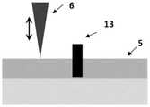
所述片上波导上设有金属纳米结构,放置在待测片上波导正上方,与波导相接触,或所述片上波导上设有波导的后端面;The on-chip waveguide is provided with a metal nanostructure, which is placed directly above the waveguide on the piece to be tested and in contact with the waveguide, or the on-chip waveguide is provided with a rear end surface of the waveguide;
所述探针以设定的频率沿竖直方向抖动,探针与片上波导中的导模倏逝场相互重叠之后,产生反向调制信号光;The probe is shaken along the vertical direction at a set frequency, and after the probe and the guided mode evanescent field in the on-chip waveguide overlap each other, a reverse modulated signal light is generated;
抖动探针与波导前向导模的倏逝场接触而形成的反射光,作为第一信号光;The reflected light formed by the contact between the dither probe and the evanescent field of the forward guided mode of the waveguide is used as the first signal light;
抖动探针造成的前向导模的功率减少量,经过金属纳米结构或波导后端面反射形成的沿波导原路返回光纤的调制光,以及直接经过金属纳米结构或波导后端面的反射后,经过抖动探针造成的功率减少量形成的沿波导原路返回光纤的调制光,两个调制光完全相同,相叠加作为第二信号光;The power reduction of the forward guided mode caused by the dithering probe, the modulated light returning to the fiber along the original path of the waveguide formed by the reflection of the metal nanostructure or the rear surface of the waveguide, and the reflection directly through the metal nanostructure or the rear surface of the waveguide, after the dithering The modulated light returned to the optical fiber along the original path of the waveguide formed by the power reduction caused by the probe, the two modulated lights are exactly the same, and superimposed as the second signal light;
所述第一信号光与第二信号光叠加,作为总的调制信号光;the first signal light and the second signal light are superimposed as the total modulated signal light;
所述窄线宽激光在透镜光纤和片上波导连接处产生反射的连续光,作为参考光;The narrow linewidth laser generates reflected continuous light at the connection between the lens fiber and the on-chip waveguide, which is used as a reference light;
所述调制信号光和参考光产生干涉,形成的干涉光反向通过透镜光纤和环形器,进入光电探测器;The modulated signal light and the reference light interfere, and the formed interference light reversely passes through the lens fiber and the circulator and enters the photodetector;
所述光电探测器用于将干涉光转化为光电流信号,所述锁相放大器用于解调光电流信号,得到解调输出信号,所述锁相放大器的解调参考信号由控制箱提供;The photodetector is used to convert the interference light into a photocurrent signal, the lock-in amplifier is used to demodulate the photocurrent signal to obtain a demodulated output signal, and the demodulation reference signal of the lock-in amplifier is provided by the control box;
所述压电陶瓷用于控制探针抖动,所述控制箱用于驱动压电陶瓷,所述电脑用于操控控制箱,并通过频谱分析,解算出探针的位置和探针位置的光强。The piezoelectric ceramic is used to control the probe shaking, the control box is used to drive the piezoelectric ceramic, and the computer is used to control the control box, and through spectrum analysis, the position of the probe and the light intensity of the probe position can be calculated .
作为优选的技术方案,所述探针放置在片上波导中心轴位置处。As a preferred technical solution, the probe is placed at the position of the central axis of the waveguide on the chip.
作为优选的技术方案,所述金属纳米结构采用300nm直径的银纳米线。As a preferred technical solution, the metal nanostructure adopts silver nanowires with a diameter of 300 nm.
本发明提供一种在片上波导上的原位损耗测量方法,包括下述步骤:The present invention provides an in-situ loss measurement method on an on-chip waveguide, comprising the following steps:
采用扫频单纵模激光器产生窄线宽扫频激光,窄线宽激光依次通过偏振控制器和环形器后,采用透镜光纤通过端面耦合方式进入片上波导中,探针以设定的频率沿竖直方向抖动,探针与片上波导中的导模倏逝场相互重叠之后,产生反向调制信号光,在片上波导上设置金属纳米结构或波导的后端面,放置在待测片上波导正上方,与波导相接触;A swept-frequency single-longitudinal-mode laser is used to generate a narrow-linewidth swept-frequency laser. After the narrow-linewidth laser passes through the polarization controller and the circulator in turn, a lensed fiber is used to enter the on-chip waveguide through end-face coupling. Jitter in the vertical direction. After the probe and the guided mode evanescent field in the on-chip waveguide overlap each other, a reverse-modulated signal light is generated. The metal nanostructure or the rear face of the waveguide is set on the on-chip waveguide and placed directly above the waveguide on the chip to be tested. in contact with the waveguide;
采用压电陶瓷控制探针抖动;Using piezoelectric ceramics to control probe jitter;
抖动探针与波导前向导模的倏逝场接触而形成的反射光,作为第一信号光;The reflected light formed by the contact between the dither probe and the evanescent field of the forward guided mode of the waveguide is used as the first signal light;
抖动探针造成的前向导模的功率减少量,经过金属纳米结构或波导后端面反射形成的沿波导原路返回光纤的调制光,以及直接经过金属纳米结构或波导后端面的反射后,经过抖动探针造成的功率减少量形成的沿波导原路返回光纤的调制光,两个调制光完全相同,相叠加作为第二信号光;The power reduction of the forward guided mode caused by the dithering probe, the modulated light returning to the fiber along the original path of the waveguide formed by the reflection of the metal nanostructure or the rear surface of the waveguide, and the reflection directly through the metal nanostructure or the rear surface of the waveguide, after the dithering The modulated light returned to the optical fiber along the original path of the waveguide formed by the power reduction caused by the probe, the two modulated lights are exactly the same, and superimposed as the second signal light;
将所述第一信号光与第二信号光叠加,作为总的调制信号光;superimposing the first signal light and the second signal light as a total modulated signal light;
所述窄线宽激光在透镜光纤和片上波导连接处产生反射的连续光,作为参考光;The narrow linewidth laser generates reflected continuous light at the connection between the lens fiber and the on-chip waveguide, which is used as a reference light;
所述调制信号光和参考光产生干涉,形成的干涉光反向通过透镜光纤和环形器,进入光电探测器;The modulated signal light and the reference light interfere, and the formed interference light reversely passes through the lens fiber and the circulator and enters the photodetector;
采用光电探测器将干涉光转化为光电流信号,采用锁相放大器解调光电流信号,得到解调输出信号;A photodetector is used to convert the interference light into a photocurrent signal, and a lock-in amplifier is used to demodulate the photocurrent signal to obtain a demodulated output signal;
采用频谱傅里叶分析,根据解调输出信号,解算出探针的位置和探针位置的相对振幅;Using spectral Fourier analysis, according to the demodulated output signal, the position of the probe and the relative amplitude of the probe position are solved;
将探针移到波导的下一个位置的中心处,采集多个探针位置和对应的相对光强,计算得到对应的损耗。Move the probe to the center of the next position of the waveguide, collect multiple probe positions and the corresponding relative light intensities, and calculate the corresponding loss.
作为优选的技术方案,所述解调输出信号采用激光频率的函数。As a preferred technical solution, the demodulated output signal is a function of the laser frequency.
作为优选的技术方案,所述将探针移到波导的一个位置的中心处,测量得到探针位置的相对振幅,具体计算公式为:As a preferred technical solution, the probe is moved to the center of a position of the waveguide, and the relative amplitude of the probe position is measured. The specific calculation formula is:
|E1|=|E0|·α0κrefl·exp(-αL1)|E1 |=|E0 |·α0 κ refl ·exp(-αL1 )
|E2|=2|E0|·r·α0κext·exp(-αL2)|E2 |=2|E0 |·r·α0 κext ·exp(−αL2 )
|Er|≡|E1|/|E2|=κrefl|(2rκext)·exp[α(L2-L1)]|Er |≡|E1 |/|E2 |=κ refl |(2rκext )·exp[α(L2 -L1 )]
其中,|E0|表示激光器输出的振幅,α0表示光纤光路中的全部振幅损耗,α为波导传输损耗系数,L1和L2代表探针和片上波导上的金属纳米结构位置,κrefl表示探针的振幅反射率,κext表示探针的振幅消光率,r为金属纳米结构或波导后端面反射率的振幅值,|Er|表示相对振幅,|E1|表示抖动探针与波导前向导模的倏逝场接触而造成的反射光振幅,|E2|表示沿波导原路返回光纤的调制光振幅。where |E0 | represents the amplitude of the laser output, α0 represents the total amplitude loss in the optical path of the fiber, α is the waveguide transmission loss coefficient, L1 and L2 represent the positions of the metal nanostructures on the probe and the on-chip waveguide, κrefl is the amplitude reflectivity of the probe, κext is the amplitude extinction ratio of the probe, r is the amplitude value of the reflectivity of the back face of the metal nanostructure or waveguide, |Er | is the relative amplitude, |E1 | The reflected light amplitude due to the evanescent field contact of the guided mode leading to the waveguide, |E2 | represents the modulated light amplitude returning to the fiber along the original path of the waveguide.
作为优选的技术方案,所述计算得到对应的损耗,具体计算公式为:As a preferred technical solution, the calculation obtains the corresponding loss, and the specific calculation formula is:

其中,α表示波导传输损耗系数,L1和L2表示探针和片上波导上的金属纳米结构位置,|Er|表示波导的两端位置的相对振幅,上标a表示测量的第一点,上标b表示测量的第二点;where α represents the waveguide transmission loss coefficient, L1 and L2 represent the position of the metal nanostructures on the probe and the on-chip waveguide, |Er | represents the relative amplitude of the two ends of the waveguide, and the superscript a represents the first point of the measurement , the superscript b represents the second point of the measurement;
作为优选的技术方案,所述计算得到对应的损耗,或采用在整段波导中测多个位置的相对幅值,通过线性拟合计算传输损耗。As a preferred technical solution, the corresponding loss is obtained by the calculation, or the transmission loss is calculated by linear fitting using relative amplitudes measured at multiple positions in the entire waveguide.
作为优选的技术方案,还包括片上器件插入损耗的测量步骤,具体步骤包括:As a preferred technical solution, it also includes the steps of measuring the insertion loss of the on-chip device, and the specific steps include:
对于波导中的某个片上器件,将探针分别放置在片上器件前端和后端波导的两侧,测量器件前后波导各自的传输损耗;For an on-chip device in the waveguide, place the probes on both sides of the front-end and back-end waveguides of the on-chip device, and measure the respective transmission losses of the waveguides before and after the device;
根据传输损耗,取延长线至片上器件位置,计算两端波导光强在片上器件处的差,得到片上器件插入损耗。According to the transmission loss, take the extension line to the position of the on-chip device, calculate the difference of the light intensity of the waveguides at both ends at the on-chip device, and obtain the insertion loss of the on-chip device.
作为优选的技术方案,还包括片上器件回波损耗的测量步骤,具体步骤包括:As a preferred technical solution, it also includes the steps of measuring the return loss of the on-chip device, and the specific steps include:
选取待测反射端面,将探针放在待测反射端面前面波导的多个位置,获取傅里叶变换曲线,从曲线中获得探针和反射端面的位置;Select the reflection end face to be measured, place the probe at multiple positions of the waveguide in front of the reflection end face to be measured, obtain the Fourier transform curve, and obtain the position of the probe and the reflection end face from the curve;
移动探针位置,得到相对振幅沿传输距离的曲线,线性拟合并延长到反射端面位置,计算出反射率r:Move the probe position to obtain a curve of relative amplitude along the transmission distance, linearly fit and extend it to the position of the reflection end face, and calculate the reflectance r:

其中,L1和L2代表探针和片上波导上的金属纳米结构位置,κrefl为振幅反射率,κext表示振幅消光率,|Er(L1=L2)|表示线性拟合延长线在反射端面位置的相对振幅。where L1 and L2 represent the positions of the metal nanostructures on the probe and the on-chip waveguide, κrefl is the amplitude reflectance, κext is the amplitude extinction ratio, and |Er (L1 =L2 )| is the linear fit extension Relative amplitude of the line at the position of the reflecting end face.
本发明与现有技术相比,具有如下优点和有益效果:Compared with the prior art, the present invention has the following advantages and beneficial effects:
(1)本发明融合了近场光学探针技术和光频域反射技术(OFDR),高空间分辨率的探针以及可灵活布置的金属纳米结构保证了对任意尺寸的波导和任意复杂度的片上光子回路进行损耗特性原位测量的可能性,包括前沿研究领域中的偏振复用/模分复用波导和器件。(1) The present invention integrates near-field optical probe technology and optical frequency domain reflectometry (OFDR) technology, high spatial resolution probes and flexible metal nanostructures to ensure on-chip waveguides of any size and any complexity. Possibilities for in situ measurement of loss properties of photonic circuits, including polarization multiplexed/mode division multiplexed waveguides and devices in cutting-edge research areas.
(2)本发明借助的光频域反射技术保证了测量操作的空间跨度可以覆盖整个片上光子回路。(2) The optical frequency domain reflectance technology used in the present invention ensures that the spatial span of the measurement operation can cover the entire on-chip photonic circuit.
(3)本发明选择相对振幅|Er|作为测量值保证了测量精度不受输入/输出光路不稳定的影响。(3) The present invention selects the relative amplitude |Er | as the measurement value to ensure that the measurement accuracy is not affected by the instability of the input/output optical path.
(4)本发明的在片上波导上的原位损耗测量装置具有结构紧凑、鲁棒性强、成本低廉、操作方便、信噪比高等优点,适合应用到复杂微纳光子回路的精确光学表征中。(4) The in-situ loss measurement device on the on-chip waveguide of the present invention has the advantages of compact structure, strong robustness, low cost, convenient operation, and high signal-to-noise ratio, and is suitable for application in the precise optical characterization of complex micro-nano photonic circuits .
附图说明Description of drawings
图1为本发明在片上波导上的原位损耗测量装置的结构示意图;1 is a schematic structural diagram of an in-situ loss measurement device on an on-chip waveguide according to the present invention;
图2为本发明在片上波导上的原位损耗测量方法流程图;FIG. 2 is a flowchart of an in-situ loss measurement method on an on-chip waveguide according to the present invention;
图3为本发明探针抖动产生调制第一信号光和第二信号光的示意图;3 is a schematic diagram of the probe jitter generating and modulating the first signal light and the second signal light according to the present invention;
图4为本发明光电流信号解调和傅里叶变换数据处理示意图;4 is a schematic diagram of photocurrent signal demodulation and Fourier transform data processing according to the present invention;
图5(a)为本发明插入损耗的测量方法示意图;Fig. 5 (a) is the schematic diagram of the measuring method of insertion loss of the present invention;
图5(b)为本发明插入损耗的测量结果示意图;Figure 5(b) is a schematic diagram of the measurement result of the insertion loss of the present invention;
图6(a)为本发明回波损耗测量方法示意图;Figure 6 (a) is a schematic diagram of the method for measuring return loss of the present invention;
图6(b)为本发明回波损耗的测量步骤中的傅里叶变换曲线示意图;Fig. 6 (b) is the Fourier transform curve schematic diagram in the measurement step of return loss of the present invention;
图6(c)为本发明回波损耗的测量步骤中的相对振幅沿传输距离的曲线示意图。FIG. 6( c ) is a schematic diagram of a curve of relative amplitude along the transmission distance in the step of measuring the return loss of the present invention.
其中,1-扫频单纵模激光器,2-偏振控制器,3-环形器,4-透镜光纤,5-片上波导,6-探针,7-压电陶瓷,8-光电探测器,9-锁相放大器,10-控制箱, 11-电脑,12-金属纳米结构,13-器件,14-反射端面。Among them, 1- Frequency Sweep Single Longitudinal Mode Laser, 2- Polarization Controller, 3- Circulator, 4- Lens Fiber, 5- On-Chip Waveguide, 6- Probe, 7- Piezoelectric Ceramic, 8- Photodetector, 9 -Lock-in amplifier, 10-control box, 11-computer, 12-metal nanostructure, 13-device, 14-reflection end face.
具体实施方式Detailed ways
为了使本发明的目的、技术方案及优点更加清楚明白,以下结合附图及实施例,对本发明进行进一步详细说明。应当理解,此处所描述的具体实施例仅仅用以解释本发明,并不用于限定本发明。In order to make the objectives, technical solutions and advantages of the present invention clearer, the present invention will be further described in detail below with reference to the accompanying drawings and embodiments. It should be understood that the specific embodiments described herein are only used to explain the present invention, but not to limit the present invention.
实施例Example
如图1所示,本实施例提供一种在片上波导上的原位损耗测量装置,包括:扫频单纵模激光器1、偏振控制器2、环形器3、透镜光纤4、片上波导5、探针 6、压电陶瓷7、光电探测器8、锁相放大器9、控制箱10、电脑11和金属纳米结构12;As shown in FIG. 1 , this embodiment provides an in-situ loss measurement device on an on-chip waveguide, including: a swept-frequency single
扫频单纵模激光器1用于产生窄线宽扫频激光(带宽为百kHz量级),窄线宽激光依次通过偏振控制器2和环形器3后,由透镜光纤4通过端面耦合方式进入片上波导中,片上波导5的上方暴露在空气中,当原子力显微镜(AFM) 的探针6与片上波导5中的导模倏逝场相互重叠之后,产生反向调制信号光;窄线宽激光在透镜光纤4和片上波导5连接处产生反射的连续光,作为参考光;调制信号光和参考光的干涉光依次反向通过透镜光纤4和环形器3,进入光电探测器8;The swept-frequency single
电脑11用于操控控制箱,控制箱10用于驱动压电陶瓷,压电陶瓷7控制探针6以设定的频率Ω沿竖直方向上下抖动(本实施例的Ω为140-250kHz,抖动幅度为100nm),由此造成调制信号光发生同样频率的强度调制;The
光电探测器8用于将连续光与调制信号光转化为光电流信号,锁相放大器9 用于采集的解调信号随激光频率变化的曲线,解调光电流信号,得到解调输出信号,锁相放大器的解调参考信号由控制箱提供;The
解调信号为激光频率的函数,对探针沿波导多个位置的解调信号进行傅里叶分析得到波导损耗;The demodulated signal is a function of the laser frequency, and the waveguide loss is obtained by Fourier analysis of the demodulated signal at multiple positions of the probe along the waveguide;
本实施例的探针采用原子力显微镜探针;The probe of this embodiment adopts an atomic force microscope probe;
片上波导回路的损耗包含了传输损耗,插入损耗和回波损耗。传输损耗指光沿着波导传输过程中的逐渐损耗,插入损耗是回路中器件或是缺陷带来的损耗,回波损耗则是代表器件的反射。The loss of on-chip waveguide loop includes transmission loss, insertion loss and return loss. Transmission loss refers to the gradual loss of light as it travels along the waveguide, insertion loss is the loss caused by a device or defect in the loop, and return loss is the reflection of the device.
在本实施例中,将探针摆放到测量不同位置,并通过测量对应位置的坐标和光强,可以进一步分别得到传输损耗,插入损耗和回波损耗;In this embodiment, the probes are placed at different positions for measurement, and by measuring the coordinates and light intensity of the corresponding positions, the transmission loss, insertion loss and return loss can be further obtained respectively;
如图2所示,本实施例还提供一种在片上波导上的原位损耗测量方法,具体步骤为:As shown in FIG. 2 , this embodiment also provides an in-situ loss measurement method on an on-chip waveguide. The specific steps are:
S1:搭建本实施例的在片上波导上的原位损耗测量装置,调节光路使得激光能够耦合进入波导中;S1: Build the in-situ loss measurement device on the on-chip waveguide of this embodiment, and adjust the optical path so that the laser can be coupled into the waveguide;
S2:将抖动的探针放置到待测波导的一个位置的中心处;S2: Place the shaking probe at the center of a position of the waveguide to be measured;
S3:扫频激光器进行频率扫描,提取锁相放大器的解调信号(随频率变化);S3: The frequency sweeping laser performs frequency scanning to extract the demodulated signal of the lock-in amplifier (varies with frequency);
S4:对该位置的解调信号进行傅里叶分析,得出探针的位置L1和相对振幅|Er|, |Er|的大小随着探针在波导上的纵向位置L1而变化;S4: Perform Fourier analysis on the demodulated signal at the position to obtain the position L1of the probe and the relative amplitude |Er |, the magnitude of |Er | varies with the longitudinal position L1of the probe on the waveguide Variety;
S5:根据具体需要测量的损耗类型选择探针需要摆放的位置,在每一个位置波导的中心处,重复步骤S3、S4;S5: Select the position where the probe needs to be placed according to the specific loss type to be measured, and repeat steps S3 and S4 at the center of the waveguide at each position;
S6:根据每个位置分析得到的探针位置和对应的相对光强信息,计算相应的损耗。S6: Calculate the corresponding loss according to the probe position and the corresponding relative light intensity information obtained by analyzing each position.
在测量步骤S3中,探针抖动产生的调制信号光沿输入光路返回至透镜光纤,经环形器3进入光电探测器8。调制信号光为第一信号光和第二信号光两部分的叠加,如图3所示,第一信号光是由抖动探针与波导前向导模的倏逝场接触而造成的反射光(κrefl为振幅反射率)。第二信号光包含两部分:由抖动探针造成的前向导模的功率减少量(κext代表该过程的振幅消光率),经过金属纳米结构或波导后端面反射(振幅反射率r)形成的沿波导原路返回光纤的调制光;先经过金属纳米结构或波导后端面反射(r),后经过抖动探针造成的功率减少量(κext)。如图3所示,两者完全相同且无法区分,相叠加构成第二信号光。考虑到κrefl和κext都是小量,本实施例不讨论更高阶的信号光产生过程,更高阶的信号光将出现在OFDR曲线中时延更大的位置,不会影响对第一信号光和第二信号光的分析。第一信号光在波导中的总传输距离为L1,随探针位置变化而变化;第二信号光在波导中的总传输距离为L2,不随探针位置变化而变化。第一信号光和第二信号光均为调制光,且在单一波长下无法被区分。In the measurement step S3 , the modulated signal light generated by the probe jitter returns to the lens fiber along the input optical path, and enters the
上述两部分信号光的振幅(|E1|和|E2|)可以用如下公式表示,The amplitudes of the above two parts of signal light (|E1 | and |E2 |) can be expressed by the following formula:
|E1|=|E0|·α0κrefl·exp(-αL1) (1a)|E1 |=|E0 |·α0 κ refl ·exp(-αL1 ) (1a)
|E2|=2|E0|·r·α0κext·exp(-αL2) (1b)|E2 |=2|E0 |·r·α0 κext ·exp(-αL2 ) (1b)
其中,|E0|代表输入激光(扫频单纵模激光器1)的振幅,α0为光纤光路(偏振控制器2、环形器3、透镜光纤4以及与波导的两次端面耦合)中的全部振幅损耗,α为波导传输损耗系数,r为金属纳米结构或波导后端面反射率的振幅值, L1和L2代表探针和金属纳米结构的位置。κrefl为探针的振幅反射率,κext为探针的振幅消光率,对于同一根探针在波导不同位置的横截面中心均保持不变。式 (1b)前面的系数2代表第二信号光是有完全相同的两部分构成。Among them, |E0 | represents the amplitude of the input laser (swept-frequency single longitudinal mode laser 1), and α0 is in the optical fiber path (
通过测量多个探针位置L1的对应振幅|E1|,利用(1)式理论上就可以测量波导的传输损耗α。然而,由于(1)式中的系数α0中包含了透镜光纤到片上波导前端面的耦合损耗,这一项损耗与光路对准程度密切相关。因此,直接测量(1)式中的两个物理量将造成最终结果α的显著误差。By measuring the corresponding amplitudes |E1 | of multiple probe positions L1 , the propagation loss α of the waveguide can theoretically be measured using equation (1). However, since the coefficient α0 in equation (1) includes the coupling loss from the lens fiber to the front face of the on-chip waveguide, this loss is closely related to the degree of optical path alignment. Therefore, direct measurement of the two physical quantities in equation (1) will cause significant errors in the final result α.
为避免上述问题,在本实施例中,采用(1a)式和(1b)式的比值:In order to avoid the above problems, in this embodiment, the ratio of formula (1a) and formula (1b) is used:
|Er|≡|E1|/|E2|=κrefl/(2rκext)·exp[α(L2-L1)] (2)|Er |≡|E1 |/|E2 |=κ refl /(2rκext )·exp[α(L2 -L1 )] (2)
在(2)式中,两束信号光的振幅之比与波导前端耦合光路的性质完全无关,只与探针造成的参数κrefl/κext以及金属纳米结构12造成的反射率等固定物理量有关,因此大大提高了测量值|Er|的可靠性和精度。每次测量中,探针放置在片上波导横截面中心轴位置处,不做横向扫描,因此节省了在波导单个位置处的逗留时间。当然,在本实施例中,探针也可以根据需要放在特定的非正中心位置,例如测量多模波导的高阶模式的时候。In equation (2), the ratio of the amplitudes of the two beams of signal light has nothing to do with the properties of the coupled optical path at the front end of the waveguide, but is only related to fixed physical quantities such as the parameters κrefl /κext caused by the probe and the reflectivity caused by the
本实施例使用了300nm直径的银纳米线作为金属纳米结构12的具体形式。金属纳米结构12放置在待测片上波导正上方,与波导相接触,它为SOI单模波导(横截面500nm×220nm,工作波长1550nm)提供了>3%量级的振幅反射率r。在本实施例中,对金属纳米结构12的材质和结构不做严格限制,只需要提供足够量的反射即可,比方说被测波导的后端面也可以造成反射也可以替代金属纳米结构。This embodiment uses silver nanowires with a diameter of 300 nm as the specific form of the
同时,从透镜光纤4引入波导端面的一部分连续光f0会被反射回光纤光路中,该部分连续光即为参考光。对于一个典型绝缘体上硅(SOI)波导,端面反射率一般在0.1%-1%量级。端面反射光不受抖动探针6的调制,保持连续光的特性。At the same time, a part of the continuous light f0 introduced into the waveguide end face from the
光电探测器8接收到的光信号为调制信号光(第一信号光和第二信号光) 和参考光的干涉光信号,之后,光电流信号在锁相放大器9处进行解调,解调频率为探针6的抖动频率Ω,得到输出信号η,解调输出信号η是激光器的输出光频率f的函数。The optical signal received by the
在测量步骤S4中,解调输出信号η(f)在电脑中进行傅里叶变换,如图4所示,得到不同信号峰与波导中传输时延的关系图。为此,本实施例在1550nm (193.4THz)附近进行了0.6THz(约5nm)范围/1.2GHz间隔的频率扫描。一次扫频测量耗时10秒,光信号的“调制”、“接收”、“解调”过程实时完成。In the measurement step S4, the demodulated output signal η(f) is subjected to Fourier transform in a computer, as shown in Figure 4, to obtain a relationship diagram between different signal peaks and the transmission delay in the waveguide. To this end, the present example performed a frequency sweep in the range of 0.6 THz (about 5 nm)/1.2 GHz interval around 1550 nm (193.4 THz). A frequency sweep measurement takes 10 seconds, and the process of "modulation", "reception" and "demodulation" of the optical signal is completed in real time.
本实施例将图4中的两个信号峰提取出来,横坐标代表它们在光波导中的传输时延,结合波导的群速度可以算出传输距离L1和L2。另一方面,图4中的信号峰的纵坐标代表探针调制产生的信号光的振幅(|E1|和|E2|,见下文),对它们的比值进行测量可以精确获得波导中导模在探针位置处的振幅。In this embodiment, the two signal peaks in FIG. 4 are extracted, and the abscissa represents their transmission delay in the optical waveguide, and the transmission distances L1 and L2 can be calculated in combination with the group velocity of the waveguide. On the other hand, the ordinate of the signal peak in Fig. 4 represents the amplitude of the signal light produced by the probe modulation (|E1 | and |E2 |, see below), and the measurement of their ratio can accurately obtain the guide in the waveguide The amplitude of the mode at the probe location.
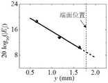
在本实施例中,对于波导传输损耗的测量,需要在步骤S5和S6中,在波导的两端(a点和b点)分别测量各自的|Er|,然后就可以直接计算这一段波导的传输损耗:In this embodiment, for the measurement of the transmission loss of the waveguide, it is necessary to measure the respective |Er | at both ends of the waveguide (point a and point b) in steps S5 and S6, and then directly calculate this section of the waveguide The transmission loss of:

也可以在整段波导中测多个位置的|Er|,然后通过线性拟合来计算传输损耗。It is also possible to measure |Er | at multiple locations in the entire waveguide, and then calculate the transmission loss by linear fitting.
由于探针可以深入到波导的任何位置,因此上述测量方法可以运用到一个片上光子集成回路的任意一段波导上,也可以应用到偏振复用/模分复用等多个传导模式并存的波导中。受益于NSOM探针的高空间分辨能力和信号调制/解调能力,与被测波导串联或并联在一起的其他波导不会对测量结果产生影响。因此本实施例实现了真正意义的“原位测量”。Since the probe can go deep into any position of the waveguide, the above measurement method can be applied to any section of the waveguide of an on-chip photonic integrated circuit, and can also be applied to the waveguide where multiple conduction modes coexist, such as polarization multiplexing/mode division multiplexing. . Benefiting from the high spatial resolution and signal modulation/demodulation capabilities of the NSOM probe, other waveguides connected in series or in parallel with the waveguide under test will not affect the measurement results. Therefore, this embodiment realizes "in-situ measurement" in the true sense.
在本实施例中,还包括片上器件插入损耗的测量步骤,对于夹在两段波导之间的片上器件或者结构的插入损耗,采用类似的方法将插入损耗和波导传输损耗区分开来,同时加以测量;In this embodiment, the step of measuring the insertion loss of the on-chip device is also included. For the insertion loss of the on-chip device or structure sandwiched between two sections of waveguides, a similar method is used to distinguish the insertion loss from the waveguide transmission loss, and at the same time add Measurement;
具体地,对于波导中的某个器件,如图5(a)所示。步骤S5和S6中,需要将探针分别放置在器件13前端和后端波导的两侧,测量器件13前后波导各自的传输损耗;根据传输损耗,取延长线至器件位置,计算两端波导光强在器件处的差,就是插入损耗,如图5(b)所示,两边两段线代表前后波导的损耗造成的光强渐变,中间的光强突变则对应插入损耗。Specifically, for a certain device in the waveguide, as shown in Fig. 5(a). In steps S5 and S6, probes need to be placed on both sides of the front and rear waveguides of the
在本实施例中,器件13指实现特定功能所需要的的器件,包括耦合器、微腔、光栅等,也可以是波导中的缺陷;器件之间由波导连接,器件会产生一定的插入损耗,是需要测量的目标;在图5(a)中采用波导中的一串空气孔作为待测的器件进行展示。In this embodiment, the
在本实施例中,还包括片上器件回波损耗的测量步骤,回波损耗就是器件的反射率,是关系到集成光子回路性能的一项重要指标。如图6(a)所示,对于某个反射端面14,在步骤S5和S6中,本实施例将探针放在它前面波导的数个位置。如图6(b)所示,图中为其中一个位置得到的傅里叶变换曲线,从该曲线中可以获得探针和反射端面的位置。移动探针位置,如图6(c)所示,得到|Er| 沿传输距离的曲线。拟合线延长到反射端面位置,可以得到公式(2)中|Er|在L1=L2处的大小。在该位置处,波导传输损耗的贡献为零,因此可以从实验拟合得到的|Er|和仿真计算得到的κrefl/κext(由于探针和波导的材料和结构已知,κrefl和κext可以通过仿真计算准确获得)计算出反射率
本发明融合了近场光学探针技术和光频域反射测量技术,具有纳米尺度高空间分辨率的近场光学探针和可灵活部署/去除的高质量金属纳米线/纳米片结构保证了对任意微小尺寸的光波导和任意结构复杂度的片上集成光子回路样品进行传输损耗/插入损耗/反射损耗参数进行原位测量的可能性。The present invention combines near-field optical probe technology and optical frequency domain reflectometry technology, near-field optical probe with nanoscale high spatial resolution and high-quality metal nanowire/nanosheet structure that can be flexibly deployed/removed to ensure that any Possibility of in situ measurement of transmission loss/insertion loss/reflection loss parameters for tiny-sized optical waveguides and samples of on-chip integrated photonic circuits of arbitrary structural complexity.
上述实施例为本发明较佳的实施方式,但本发明的实施方式并不受上述实施例的限制,其他的任何未背离本发明的精神实质与原理下所作的改变、修饰、替代、组合、简化,均应为等效的置换方式,都包含在本发明的保护范围之内。The above-mentioned embodiments are preferred embodiments of the present invention, but the embodiments of the present invention are not limited by the above-mentioned embodiments, and any other changes, modifications, substitutions, combinations, The simplification should be equivalent replacement manners, which are all included in the protection scope of the present invention.
Claims (10)


Priority Applications (1)
| Application Number | Priority Date | Filing Date | Title |
|---|---|---|---|
| CN202010978883.9ACN112197941B (en) | 2020-09-17 | 2020-09-17 | In-situ loss measuring device and method on-chip waveguide |
Applications Claiming Priority (1)
| Application Number | Priority Date | Filing Date | Title |
|---|---|---|---|
| CN202010978883.9ACN112197941B (en) | 2020-09-17 | 2020-09-17 | In-situ loss measuring device and method on-chip waveguide |
Publications (2)
| Publication Number | Publication Date |
|---|---|
| CN112197941A CN112197941A (en) | 2021-01-08 |
| CN112197941Btrue CN112197941B (en) | 2022-06-21 |
Family
ID=74015347
Family Applications (1)
| Application Number | Title | Priority Date | Filing Date |
|---|---|---|---|
| CN202010978883.9AActiveCN112197941B (en) | 2020-09-17 | 2020-09-17 | In-situ loss measuring device and method on-chip waveguide |
Country Status (1)
| Country | Link |
|---|---|
| CN (1) | CN112197941B (en) |
Family Cites Families (5)
| Publication number | Priority date | Publication date | Assignee | Title |
|---|---|---|---|---|
| EP2280256B1 (en)* | 2003-10-27 | 2016-11-16 | The General Hospital Corporation | Method and apparatus for performing optical imaging using frequency-domain interferometry |
| JP2006322843A (en)* | 2005-05-19 | 2006-11-30 | Nippon Telegr & Teleph Corp <Ntt> | Optical transmission loss measuring system, measuring device and cap thereof, and optical transmission loss measuring method |
| CN101206155A (en)* | 2006-12-21 | 2008-06-25 | 中国科学院半导体研究所 | Measuring method and measuring device for optical waveguide transmission loss |
| CN100533095C (en)* | 2008-01-21 | 2009-08-26 | 浙江大学 | Device and method for testing basic structural parameters of optical waveguide ring resonator |
| CN109387356B (en)* | 2018-08-31 | 2020-11-13 | 中国电子科技集团公司第五十五研究所 | A kind of optical waveguide transmission loss measurement method |
- 2020
- 2020-09-17CNCN202010978883.9Apatent/CN112197941B/enactiveActive
Also Published As
| Publication number | Publication date |
|---|---|
| CN112197941A (en) | 2021-01-08 |
Similar Documents
| Publication | Publication Date | Title |
|---|---|---|
| CN101949685B (en) | Fiber laser self-mixing interferometer and measurement method thereof | |
| JP5376619B2 (en) | Electromagnetic field measuring device | |
| CN101319878B (en) | Method and device for high-precision large-range measuring size of optical fiber | |
| JP2012515350A (en) | Optical imaging for optical device inspection | |
| CN102281107A (en) | Apparatus and method for measuring dispersion of optical fiber optics | |
| CN107917669B (en) | Demodulation method of optical fiber displacement sensor | |
| CN106289726A (en) | A kind of photon band-gap optical fiber backscattering distributed measurement method and device | |
| CN110319940A (en) | The laser fiber interferometer diagnostic system of high-density plasma density measure | |
| CN110118532A (en) | The dual wavelength nonlinear displacement demodulation method and system of optical fiber Fabry-Perot displacement sensor | |
| CN103017670B (en) | A kind of coating film on glass quality detecting system based on frustrated total reflection | |
| JP3388227B2 (en) | Optical dispersion measuring apparatus and measuring method using the same | |
| Han et al. | Integrated silicon photonics ofdr system for high-resolution distributed measurements based on Rayleigh backscattering | |
| CN112747682B (en) | Liquid film thickness measurement system based on light carries microwave interference | |
| CN109239404A (en) | The holeless near field optic micro imaging method of optical path reflecting interferometer is total to based on all -fiber | |
| CN112197941B (en) | In-situ loss measuring device and method on-chip waveguide | |
| CN107796422B (en) | Optical fiber displacement sensor demodulating equipment | |
| CN107806981B (en) | Measuring device for beat length of polarization maintaining optical fiber | |
| JP4463828B2 (en) | Measuring method, measuring apparatus and measuring program for wavelength dispersion of optical waveguide | |
| Toda et al. | Integrated-optic heterodyne interferometer for displacement measurement | |
| CN101825435A (en) | All-fiber-optic displacement measuring method and device thereof | |
| CN117804346A (en) | Optical fiber interference absolute length difference measurement system | |
| JP4027352B2 (en) | Optical fiber probe device | |
| CN207219136U (en) | Optical-fiber laser interference electron density measurement system based on mathematics method of comparison | |
| CN118392824B (en) | Device and method for synchronously measuring thickness and group refractive index of birefringent crystal | |
| Yan et al. | Response of local evanescent array-coupled biosensors to organic nanofilms |
Legal Events
| Date | Code | Title | Description |
|---|---|---|---|
| PB01 | Publication | ||
| PB01 | Publication | ||
| SE01 | Entry into force of request for substantive examination | ||
| SE01 | Entry into force of request for substantive examination | ||
| GR01 | Patent grant | ||
| GR01 | Patent grant |