CN1121741C - Semiconductor device and manufacturing method thereof - Google Patents
Semiconductor device and manufacturing method thereofDownload PDFInfo
- Publication number
- CN1121741C CN1121741CCN92110004.3ACN92110004ACN1121741CCN 1121741 CCN1121741 CCN 1121741CCN 92110004 ACN92110004 ACN 92110004ACN 1121741 CCN1121741 CCN 1121741C
- Authority
- CN
- China
- Prior art keywords
- channel formation
- formation region
- interlayer dielectric
- region
- source
- Prior art date
- Legal status (The legal status is an assumption and is not a legal conclusion. Google has not performed a legal analysis and makes no representation as to the accuracy of the status listed.)
- Expired - Lifetime
Links
Images


Landscapes
- Thin Film Transistor (AREA)
- Liquid Crystal (AREA)
Abstract
Description
Translated fromChinese本发明涉及有源矩阵式电光器件,更具体地说,涉及一种可应用于有源矩阵式(active-matrix)液晶电光器件之类并具有最佳开关特性的场效应晶体管。本发明还涉及制造这种场效应晶体管的方法。The present invention relates to an active-matrix electro-optical device, and more particularly to a field-effect transistor applicable to active-matrix liquid crystal electro-optic devices and the like and having optimum switching characteristics. The invention also relates to a method of manufacturing such a field effect transistor.
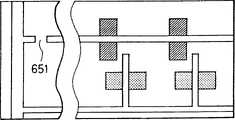
现有技术用于有源矩阵式液晶电光器件的薄膜绝缘栅场效应晶体管的结构,如图2所示。在绝缘基片9上形成有阻挡层8。具有源区4,漏区5和沟道区3的半导体层形成于阻挡层8上。在该半导体层上层叠有栅绝缘膜2和栅极1。层间绝缘膜12形成在栅绝缘膜2和栅极1上。源极6和漏极7形成于层间绝缘膜12和半导体层上。The structure of a thin film IGFET used in an active matrix liquid crystal electro-optic device in the prior art is shown in FIG. 2 . On the
这种现有技术的绝缘栅FET的制造,按序描述如下:首先,借助用SiO2作为耙的溅射法在玻璃基片9上产生阻挡层8。然后,借助等离子体加速的CVD法形成半导体层并为构成具有源,漏和沟道区的半导体层而构图。然后,溅射氧化硅,以形成栅绝缘膜2。接着,利用低压CVD法,产生被高掺磷并用于构成栅极的导电层。然后,为形成栅极1而对导电层构制图样。此后用该栅极作掩模,植入掺杂剂的离子,从而制成源区4,和漏区5。然后,对该层制品进行热处理,以激活它。The fabrication of this prior art insulated gate FET is described in sequence as follows: First, a
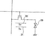
以这种方式制成的绝缘栅FET,其栅极1沿沟道纵向所占的长度基本上与标号10所表示的沟道长度相同。在n构道结构情况下,这种结构的FET之电流一电压特性示于图3。这种FET的缺点在于:在反偏区13中,漏电流随着加在源和漏区间的电压升高而增大。在该器件用于有源矩阵式液晶电光器件时,若漏电流以这这种方式增大的话,则在非写周期期间,借助写电流30而储存于液晶29中的电荷就象图5(A)中所示通过该器件漏电部分的漏电电流31那样被释放掉了。照这样,是不可能获得良好对比度的。In the insulated gate FET manufactured in this way, the length occupied by the
解决这一问题的传统做法是如图5(B)所示,附加一个用以保持电荷的电容器32。然而,为构成这种电容器,必须要有由金属互连制成的电容电极。这导致孔径比(aperture ratio)的减小。还有,据说,孔径比是通过用ITO的透明电极来制造这种电容而得以改善的。然而,该方法需要一多余工序(excess process),因而不受欢迎。The conventional way to solve this problem is to add a capacitor 32 for holding charge as shown in FIG. 5(B). However, to form such a capacitor, it is necessary to have capacitor electrodes made of metal interconnections. This results in a reduction in aperture ratio. Also, it is said that the aperture ratio is improved by making this capacitor with a transparent electrode of ITO. However, this method requires an excess process and thus is not popular.
在这种绝缘栅FET的源和漏极中只有其中之一同一个电容性器件或一电容器相连,而且该晶体管用作开关器件的场合下,例如,在众所周知的一晶体管/单元型(1 transistor/cell type)的动态随机存取存储器(DRAM)的情况下,或在其每个象素具有如图5(A)或5(B)所示电路的有源液晶显示器的情况下,人们知道:电容器上的电压是会因为栅极与漏极或源极之间存在寄生电容而变化的。Where only one of the source and drain of such an insulated gate FET is connected to a capacitive device or a capacitor, and the transistor is used as a switching device, for example, in the well-known one transistor/cell type (1 transistor/ In the case of a dynamic random access memory (DRAM) of the cell type), or in the case of an active liquid crystal display having a circuit as shown in Fig. 5(A) or 5(B) for each pixel, it is known that: The voltage across the capacitor varies due to the parasitic capacitance between the gate and the drain or source.
这个电压的变量V与栅压VG和寄生电容成正比,而与电容器和寄生电容的电容量之和成反比。因此,通常在制造该晶体管时借助自动调整技术去减小寄生电容量,从而抑制电压的变化。但是,当器件的尺寸减小时,寄生电容的影响则增大到即使采用自动调整法也不容忽略不计的程度。The variable V of this voltage is proportional to the gate voltage VG and the parasitic capacitance, and inversely proportional to the sum of the capacitance of the capacitor and the parasitic capacitance. Therefore, the automatic adjustment technology is usually used to reduce the parasitic capacitance when manufacturing the transistor, so as to suppress the voltage change. However, as the size of the device decreases, the influence of parasitic capacitance increases to such an extent that it cannot be ignored even with the automatic adjustment method.
就设法减小变量V而言,现已提出一种新的方法。具体地说,如图5(B)所示,除本身的容性器件外还并联有一电容器,以增大该容性器件的视在电容量。然而,正如前而已述,对DRAM而言,该电容器的面积增大不能被忽略不计。对液晶显示器而言,不能忽略不计数值孔径的减小。In terms of trying to reduce the variable V, a new approach has been proposed. Specifically, as shown in FIG. 5(B), in addition to the capacitive device itself, a capacitor is connected in parallel to increase the apparent capacitance of the capacitive device. However, as mentioned earlier, for DRAM, the area increase of this capacitor cannot be ignored. For liquid crystal displays, the reduction in insignificant numerical aperture cannot be ignored.
本发明的一个目的就是提供一种没有上述诸问题的绝缘栅FET。SUMMARY OF THE INVENTION An object of the present invention is to provide an insulated gate FET free from the above-mentioned problems.
上述目的的实现途径是将绝缘栅FET中的沟道长度,即源区与漏区的间距,制作成大于栅极沿沟道的纵向(沟道长度方向)所取的长度,从而使偏移(offset)区分别形成于同源区和漏区相接触的那些沟道区的部位内。所述偏移区不受栅极的电场作用,或受到极微弱的栅极电场的作用。这种器件的电流一电压特性示于图4中。The way to achieve the above purpose is to make the channel length in the insulated gate FET, that is, the distance between the source region and the drain region, larger than the length of the gate along the longitudinal direction of the channel (channel length direction), so that the offset (offset) regions are respectively formed in those portions of the channel region that are in contact with the source region and the drain region. The offset region is not affected by the electric field of the grid, or is affected by a very weak electric field of the grid. The current-voltage characteristics of this device are shown in FIG. 4 .
本发明的另一目的是提供前段所描述的这种绝缘栅FET的加工方法。Another object of the present invention is to provide a method for processing such an insulated gate FET as described in the preceding paragraph.
本发明的其它目的及特征将在以下对其的说明中显现。Other objects and features of the present invention will appear in the following description thereof.
图1是根据本发明的一种半导体器件的截面视图;1 is a cross-sectional view of a semiconductor device according to the present invention;
图2是传统半导体器件的截面视图;2 is a cross-sectional view of a conventional semiconductor device;
图3是表示图2所示传统型半导体器件的电流—电压特性曲线图;Fig. 3 is a graph showing the current-voltage characteristics of the conventional semiconductor device shown in Fig. 2;
图4是显示图1所示新型半导体器件的电流电压特性曲线图;Fig. 4 is a graph showing the current-voltage characteristics of the novel semiconductor device shown in Fig. 1;
图5(A)和5(B)是传统型有源矩阵式液晶电光器件的部分电路图;Fig. 5 (A) and 5 (B) are the partial circuit diagrams of traditional type active matrix type liquid crystal electro-optic device;
图6是根据本发明实例1的有源矩阵式液晶电光器件的一部分电路图;Fig. 6 is a part circuit diagram of the active matrix type liquid crystal electro-optical device according to the example 1 of the present invention;
图7是图6所示新型有源矩阵式液晶电光器件的那部分平面视图;Fig. 7 is that part plan view of novel active matrix type liquid crystal electro-optical device shown in Fig. 6;
图8(A)至8(F)是图6和7所示新型有源矩阵式液晶电光器件的部分截面视图,示出了制造该器件的步骤;8(A) to 8(F) are partial cross-sectional views of the novel active-matrix liquid crystal electro-optical device shown in FIGS. 6 and 7, illustrating the steps of manufacturing the device;
图9是表示本发明实例2的P-沟道TFT(薄膜晶体管)的电流电压特性曲线图;9 is a graph showing the current-voltage characteristics of a P-channel TFT (thin film transistor) of Example 2 of the present invention;
图10是表示本发明实例2的n沟道TFT的电流—电压特性曲线图;Fig. 10 is a graph showing the current-voltage characteristics of the n-channel TFT of Example 2 of the present invention;
图11是说明实例2的漏极电流对阳极化膜的厚度的关系曲线图;11 is a graph illustrating the relationship between drain current and the thickness of anodized film of Example 2;
图12是说明实例2之阈值电压对阳极化膜之厚度的关系曲线图;12 is a graph illustrating the relationship between the threshold voltage of Example 2 and the thickness of the anodized film;
图13是说明实例2之电场迁移率对阳极化膜之厚度的关系曲线图;Fig. 13 is a graph illustrating the relationship between the field mobility of Example 2 and the thickness of the anodized film;
图14(A)至14(D)是实例2的薄膜晶体管的部分截面示图,示出了制造该器件的次序;14(A) to 14(D) are partial cross-sectional views of the thin film transistor of Example 2, showing the sequence of manufacturing the device;
图15(A)至15(C),是图14(A)至14(D)所示薄膜晶体管的顶视图,示出了该器件的制造次序;15(A) to 15(C), are top views of the thin film transistor shown in FIGS. 14(A) to 14(D), showing the manufacturing sequence of the device;
图16(A)至16(F)是本发明实例1的有源矩阵式液晶电光器件的部分截面视图;16(A) to 16(F) are partial cross-sectional views of the active matrix liquid crystal electro-optical device of Example 1 of the present invention;
图17(a)和17(b)是表示薄膜晶体管特性的曲线图;17(a) and 17(b) are graphs showing characteristics of thin film transistors;
图17(c)至17(f)是说明本发明薄膜晶体管之工作原理的示意图;17(c) to 17(f) are schematic diagrams illustrating the working principle of the thin film transistor of the present invention;
图18(A)至18(D)是本发明实例5之薄膜晶体管的截面视图,示出了制造该器件的次序;18(A) to 18(D) are cross-sectional views of the thin film transistor of Example 5 of the present invention, showing the sequence of manufacturing the device;
图19(A)至19(D)是本发明实例6的薄膜晶体管的截面视图;示出了制造该器件的次序;19(A) to 19(D) are cross-sectional views of a thin film transistor of Example 6 of the present invention; show the sequence of manufacturing the device;
图20是本发明实例6之有源矩阵式液晶电光器件的平面视图;Fig. 20 is the plane view of the active matrix type liquid crystal electro-optical device of the example 6 of the present invention;
图21是本发明实例7的有源矩阵式液晶电光器件的一部分电路图;Fig. 21 is a part of the circuit diagram of the active matrix type liquid crystal electro-optic device of example 7 of the present invention;
图21(A)和21(B)是说明图21所示有源矩阵式液晶电光器件的工作的原理图;Fig. 21 (A) and 21 (B) are the schematic diagrams illustrating the work of the active matrix liquid crystal electro-optical device shown in Fig. 21;
图22(A)至22(C)是本发明实例6的薄膜晶体管的顶视图,示出了制造该器件的顺序。22(A) to 22(C) are top views of the thin film transistor of Example 6 of the present invention, showing the sequence of manufacturing the device.
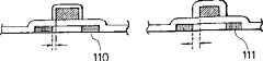
参见图1,该图示出了本发明场效应晶体管的基本结构。该晶体管具有绝缘基片105和建立在该基片105上的阻挡层104。成为源区100,漏区101和沟道区109的半导体层建立在阻挡层104上。在沟道区109上形成有栅绝缘膜110。栅极111形成于栅绝缘膜110上。属于绝缘层的氧化层112形成于栅极111上。该氧化层112是通过对一种可被阳极化的材料进行阳极化而形成的。源极102及漏极103是使其分别同源区和漏区相接触而形成的。图1中未示出层间隔离膜,但在栅极或连至该栅极的引线与源、漏区,或连至源或漏极的引线之间的寄生电容量成为问题的场合可用先有技术的同样方式形成层间隔离膜。这方面的实例将在后面描述。Referring to Fig. 1, this figure shows the basic structure of the field effect transistor of the present invention. The transistor has an insulating
仍参见图1,成为栅极111和氧化层112的栅极部分是由可被阳极化的材料制成。该栅极部分的表面部分被阳极化而形成氧化层112。待植入离子的源区100和漏区101之间的距离,即,沟道长度108比栅极111沿沟道纵向所占的实际长度长出大约两倍于氧化层112的厚度值。所述栅极部分包含金属或半导体。栅极部分的材料主要选自钛(Ti),铝(Al),钽(Ta),铬(Cr)和硅(Si)之一。另一方面,栅极部分也可由这些材料中的某些合金制成。Still referring to FIG. 1 , the portion of the gate that becomes
因此,沟道区109的那些位于从形成于栅极两侧上的氧化层112部分引伸的栅绝缘膜110的相对两侧上之部分106和107不受栅极电场的作用或经受比直接处于栅极下的那些部分要弱得多的电场作用。这些区域106和107,特别是在结晶度和剂量方面可与沟道区相比的场合下,此后称其为偏移区。Therefore, those
这些区域106和107可由掺杂的非晶体材料构成。更严格地说,区域106和107的唯一必要条件是其结晶度次于相邻的源区100和漏区101。例如,若源区100和漏区101是由具有大结晶颗粒的多晶硅构成的话,则区域106和107只需由结晶度稍优于非晶硅的半非晶硅或非晶硅构成。若区域100和101是由半非晶硅构成,则区域106和107可由非晶硅构成。当然,这些非晶体材料是需要经过充分处理而使其呈现半导体性能的。例如,为了最大限度地减少空键,必须借助氢或某种囟素来充分减少这类键。These
通过形成这些非晶体区就可获得如图17(a)所示的良好的TFT特性。图17(b)示出了先有技术的绝缘栅晶体管结构的一薄膜晶体管的电流一电压特性。正如比较这些特性曲线时可见到的,当采用先有技术方法时,可观测到反向漏电流很大。根据本发明方法,由于形成大致为非晶体的区域,从而改善了该特性。也就是说,掺杂非晶区的形成获得了如先前已述的偏移区的形成同样的优点。By forming these amorphous regions, good TFT characteristics as shown in FIG. 17(a) can be obtained. FIG. 17(b) shows the current-voltage characteristics of a thin film transistor of the prior art IGS structure. As can be seen when comparing these characteristic curves, when the prior art method is used, a large reverse leakage current is observed. According to the method of the invention, this characteristic is improved due to the formation of substantially amorphous regions. That is, the formation of the doped amorphous region achieves the same advantages as the formation of the offset region described previously.
为什么非晶体区域的形成会改善该特性是无法完全理解的。一个可能的原因如下所述:在非晶体区域中,添加的掺杂元素以低于晶体区域中的速率被离子化。因此,若以相同剂量添加掺杂剂,则非晶体区表现它们具有较低的掺杂剂浓度。也就是说,形成了大致类似于轻参杂的漏区的区域。例如,非晶态硅室温下的电离率为0.1-10%,这比几乎为100%电离率的单晶或多晶半导体要低得多。Why the formation of amorphous regions improves this property is not fully understood. One possible reason is as follows: In the amorphous region, the added dopant element is ionized at a lower rate than in the crystalline region. Therefore, if dopants are added at the same dose, the amorphous regions appear to have a lower dopant concentration. That is, a region approximately similar to a lightly doped drain region is formed. For example, the ionization rate of amorphous silicon at room temperature is 0.1-10%, which is much lower than that of single crystal or polycrystalline semiconductors, which have an ionization rate of almost 100%.
另一可能原因是非晶态的带隙大于结晶态的带隙。例如,这可通过图17(e)和17(f)的能带图来解释。就通常轻掺杂的漏区结构晶体管而言,源、沟道和漏区之间的能带示于图17(c)和17(d)中。中段提升部分表示沟道区。阶梯部分表示轻掺杂漏区。图17(c)示出了栅极未加电压时的情况。当栅极施加以大的负电压时,便出现图17(d)所示情况。此时,在源区与沟道区之间以及沟道区与漏区之间存在禁带,从而防止诸如电子和空穴之类的载流子的运动。不过,这些载流子可利用隧道效应或以跳过带隙内的陷阱能级(traplevel)的方式通过带隙。在不属轻掺杂漏区结构的一般薄膜晶体管(TET)中,带隙宽度较小,故更易于流过电流。这被认为是反向漏泄。这种现象对TFT来说尤为显著,并可能由归因于晶粒边界的许多陷阱能级所引起,因为TFT是由诸如多晶体等的多相材料制成的。Another possible reason is that the band gap of the amorphous state is larger than that of the crystalline state. For example, this can be explained by the energy band diagrams of Figures 17(e) and 17(f). For conventional lightly doped drain structure transistors, the energy bands between the source, channel and drain regions are shown in Figures 17(c) and 17(d). The raised portion in the middle represents the channel region. The stepped part represents the lightly doped drain region. Figure 17(c) shows the situation when no voltage is applied to the gate. When a large negative voltage is applied to the grid, the situation shown in Figure 17(d) occurs. At this time, forbidden bands exist between the source region and the channel region and between the channel region and the drain region, thereby preventing movement of carriers such as electrons and holes. However, these carriers can pass through the bandgap by tunneling or by jumping over trap levels within the bandgap. In general thin-film transistors (TETs) that do not have a lightly doped drain structure, the bandgap width is smaller, so it is easier to flow current. This is known as reverse leakage. This phenomenon is particularly pronounced for TFTs, and may be caused by many trap levels due to grain boundaries, since TFTs are made of heterogeneous materials such as polycrystals.
当增大轻掺杂漏区中的带隙时,上述的反向漏电流便减小。这种实例示于图17(e)和17(f)中。图17(e)示出了未将电压施加到栅极时的情况,图17(f)示出栅极加有大的负电压时的情况。当如图17(f)所示施加一负压时,则正如比较图17(f)与图17(d)时所见,源区和沟道区之间的带隙宽度以及沟道区和漏区之间的带隙宽度均大于图17(d)所示情况中的相应宽度。隧道效应大大地受隧道阻挡层的宽度(在此情况下为带隙宽度)的影响。随着带隙宽度的稍微增大载流子穿透带隙的概率大大减小。再者,经由局部能级的跃迁是一种合成隧道效应,因此,当带隙宽度增大时,穿述带隙的概率会急剧下降。由于这些理由,故认为使轻掺杂漏区具有大带隙是有利的。非晶硅的带隙是1.5至1.8eV,而多晶硅的带隙为1.1eV。若轻掺杂漏区采用具有这样宽带隙的材料,则会产生相当理想的情况。When the bandgap in the lightly doped drain region is increased, the above-mentioned reverse leakage current is reduced. Examples of this are shown in Figures 17(e) and 17(f). Figure 17(e) shows the situation when no voltage is applied to the gate, and Figure 17(f) shows the situation when a large negative voltage is applied to the gate. When a negative pressure is applied as shown in Figure 17(f), then as seen when comparing Figure 17(f) with Figure 17(d), the bandgap width between the source region and the channel region and the channel region and The bandgap widths between the drain regions are all larger than the corresponding widths in the case shown in FIG. 17(d). Tunneling is greatly influenced by the width of the tunnel barrier (in this case, the bandgap width). As the band gap width increases slightly, the probability of carriers penetrating the band gap decreases greatly. Furthermore, the transition through local energy levels is a kind of synthetic tunneling effect, so when the bandgap width increases, the probability of penetrating the bandgap decreases sharply. For these reasons, it is considered advantageous to have a lightly doped drain region with a large bandgap. Amorphous silicon has a band gap of 1.5 to 1.8 eV, while polysilicon has a band gap of 1.1 eV. If the lightly doped drain region uses a material with such a wide bandgap, a rather ideal situation will result.
为制造根据本发明的半导体器件,尤其是制造具有上述偏移区的半导体器件,在成为源区,漏区和沟道区的半导体层以及栅绝缘层110形成之后用能被阳极化的材料建立栅极部分接着,将赋予半导体层为P型或n型的掺杂剂离子植入该半导体层,以形成源区100和漏区101。此后,对栅极部分的表面进行阳极化(阳极氧化),以产生栅极111和氧化层112。此后,再进行热处理或其它步骤。In order to manufacture a semiconductor device according to the present invention, especially a semiconductor device having the above-mentioned offset region, after forming the semiconductor layer and the
另一种方法是:先形成半导体层和栅绝缘层110,再用能被阳极化的材料制作栅极部分,接着,对栅极部分的表面进行阳极化(阳极氧化),以形成栅极111和氧化层112。然后,将掺杂剂离子植入半导体层,以赋予其为P或n型,同时形成源区100和漏区101。此后,完成热处理。Another method is: first form the semiconductor layer and the
在实施这些步骤过程中,可容易地和可靠地制作其沟造长度大于沿沟道纵向所占的栅极长度的绝缘栅FET,而不会产生因掩膜偏差所引起的性能变化。In carrying out these steps, an insulated gate FET having a channel length greater than the gate length occupied longitudinally of the channel can be easily and reliably fabricated without performance variations due to mask deviation.
制造具有非晶体区的新型半导体器件的另一种方法是一开始形成成为源区,漏区和沟道区的半导体层以及栅绝缘层110。然后,用能被阳极化的材料制造栅极部分。接着,植入掺杂剂离子,以使半导体层掺杂成P型或n型。因此,使半导体层制成非晶体的。形成源区100,漏区101,及其毗邻的非晶体区106和107。此后,对栅极部分的表面部分进行阳极化,以形成栅极111和氧化层112。此时,对栅极表面进行氧化再处理。然后,当借助应用激光退火或闪光灯退火技术的自调整工艺将栅极部分用作掩膜时,只有源区100和漏区101可被再结晶。这一工艺过程属于自调整型式,因为栅极部分遮蔽了位于栅极部分下面的底层掺杂区,故禁止了这些掺杂区的再结晶。Another method of fabricating a new type of semiconductor device having an amorphous region is to initially form the semiconductor layers to be the source, drain and channel regions and the
在利用离子植入工艺的地方,由离子的二次扩散引起的掺杂区的范围(spreading)可根据离子的加速能量而算出。再者,栅极的再处理是由氧化层的厚度确定的,因此,再处理也被取作为一个设计参数。根据本发明,可通过精确设计而达到栅极和掺杂区之间位置关系的最佳化。更具体地说,可按公差小于10nm来控制氧化层的厚度。此外,在离子植入期间所产生的二次散射可按与此同一数量级的允差来加以控制。因此,制造期间,可将位置关系控制到允差小于10nm。Where the ion implantation process is used, the spreading of the doped region caused by the secondary diffusion of ions can be calculated according to the acceleration energy of the ions. Furthermore, gate reprocessing is determined by the thickness of the oxide layer, so reprocessing is also taken as a design parameter. According to the present invention, the optimization of the positional relationship between the gate and the doped region can be achieved through precise design. More specifically, the thickness of the oxide layer can be controlled with a tolerance of less than 10 nm. In addition, secondary scattering generated during ion implantation can be controlled within tolerances of the same order. Therefore, during manufacturing, the positional relationship can be controlled to a tolerance of less than 10 nm.
由此可见,本发明无需更精确的掩膜调整。由本发明方法生产的产品损耗率是很低的。更确切地说,本发明器件具有大大改善的各项性能。下面给出了本发明的一些实例。实例1It can be seen that the present invention does not require more precise mask adjustment. The product loss rate produced by the method of the present invention is very low. More precisely, the devices of the present invention have greatly improved properties. Some examples of the invention are given below. Example 1
采用根据本发明的对角线为1英寸的液晶电光器件制造用于电视摄象机的反光镜。该器件有387×128个象素,该反光镜用高迁移率的TFT(薄膜晶体管)在低温工艺中制得。用于本例中的液晶电光器件之基片上各有源元件的配置示于图7中。图6是本例的电路示意图。制造步骤示于沿直线A-A′和B-B′所裁取的图8(A)至8(F)中。沿直线A-A′所取横截面表示一n沟道TFT。沿直线B-B′所取横截面表示一P沟道TFT。A mirror for a television camera was manufactured using a liquid crystal electro-optical device having a diagonal of 1 inch according to the present invention. The device has 387×128 pixels, and the mirror is fabricated in a low-temperature process using high-mobility TFT (thin-film transistor). The arrangement of active elements on the substrate used in the liquid crystal electro-optical device in this example is shown in FIG. Figure 6 is a schematic circuit diagram of this example. The manufacturing steps are shown in Figs. 8(A) to 8(F) taken along lines A-A' and B-B'. A cross section taken along the line A-A' shows an n-channel TFT. A cross section taken along the line B-B' shows a P-channel TFT.
在图8(A)中,玻璃基片51由一种廉价材料构成并经历了700℃以下,例如600℃左右,的热处理。借助磁控管RF(高频)溅射工艺,在玻璃基片51上溅射氧化硅至厚度为1000至3000埃(),以形成阻挡层52。其环境条件是100%的氧气。在150℃温度下形成该膜。磁控管输出功率为400至800度。压力为0.5Pa。所用的耙是由石英或硅的一种单晶体构成。沉积率为30至100/分。In FIG. 8(A), a glass substrate 51 is formed of an inexpensive material and subjected to heat treatment at 700°C or lower, for example, around 600°C. The barrier layer 52 is formed by sputtering silicon oxide on the glass substrate 51 to a thickness of 1000 to 3000 angstroms (Å) by means of a magnetron RF (high frequency) sputtering process. Its ambient conditions are 100% oxygen. The film was formed at a temperature of 150°C. Magnetron output power is 400 to 800 degrees. The pressure is 0.5Pa. The rake used consists of a single crystal of quartz or silicon. The deposition rate is 30 to 100 Å/min.
用低压CVD(LPCVD),溅射,或等离子加速CVD方法在该阻挡层52上形成硅膜。在用低压CVD法形成硅膜的场合,则要在低于结晶温度100至200℃(例如450至550℃)的某一温度,例如在530℃,下,将乙硅烷(Si2H6)或三硅烷(Si3H8)加入CVD设备中,反应炉内部压力为30至300Pa。淀积率为50至250/分钟。为使P沟道和n沟道TFT具有大致均匀的阈值电压Vth,可将乙硼烷形式的浓度为1×1015至1×1018原子/cm3的硼添加至该膜。A silicon film is formed on the barrier layer 52 by low pressure CVD (LPCVD), sputtering, or plasma accelerated CVD. In the case of forming a silicon film by low-pressure CVD, disilane (Si2 H6 ) should be added at a temperature of 100 to 200°C (for example, 450 to 550°C) lower than the crystallization temperature, for example, at 530°C. Or trisilane (Si3 H8 ) is added into the CVD equipment, and the internal pressure of the reaction furnace is 30 to 300Pa. The deposition rate is 50 to 250 Å/min. In order for p-channel and n-channel TFTs to have substantially uniform threshold voltage Vth, boron in the form of diborane at a concentration of 1×10¹⁵ to 1×10¹⁸ atoms/cm3 may be added to the film.
在用溅射法的情况下,进行溅射前的背压为1×10⁻⁵pa或更小。用一种单晶硅作为耙。该工艺过程在添加了20-80%氢气的氩气环境下实现。例如,氩气占20%,而氢气占80%,在150℃时形成该膜。RF的频率为13.56MHz。溅射输出功率为400至800瓦。压力为0.5Pa。In the case of using the sputtering method, the back pressure before sputtering is 1×10⁻⁵ Pa or less. A single crystal silicon is used as a rake. The process is realized under an argon atmosphere with 20-80% hydrogen added. For example, argon is 20% and hydrogen is 80%, and the film is formed at 150°C. The frequency of RF is 13.56MHz. The sputtering output power is 400 to 800 watts. The pressure is 0.5 Pa.
在用等离子加速CVD法形成硅膜的场合,例如,温度为300℃。采用甲硅烷(SiH4)或乙硅烷(Si2H6)。这类材料被导入PCVD设备。在施加13.56MHz的RF电功率下形成硅膜。When the silicon film is formed by plasma accelerated CVD, the temperature is, for example, 300°C. Monosilane (SiH4 ) or disilane (Si2 H6 ) is used. Such materials are directed into PCVD equipment. The silicon film was formed under application of RF electric power of 13.56 MHz.
通过采用这些方法而形成的硅膜的氧含量最好为5×10²¹原子/cm3或更小。若氧浓度高时,则难以结晶出硅膜。结果,必需提升热处理温度或延长热处理的时间。反之,若氧的浓度过低,则由于背光引起断开状态下的漏电流增大。因此,其适宜浓度范围为4×1019至4×1021原子/cm3。氢浓度为4×1020原子/cm3,它是4×1022原子/cm3的硅浓度的1原子百分比。The oxygen content of the silicon film formed by employing these methods is preferably 5 x 10²¹ atoms/cm3 or less. When the oxygen concentration is high, it is difficult to crystallize the silicon film. As a result, it is necessary to raise the heat treatment temperature or extend the time of heat treatment. Conversely, if the concentration of oxygen is too low, the leakage current in the off state increases due to the backlight. Therefore, its suitable concentration range is 4×10¹⁹ to 4×10²¹ atoms/cm3 . The hydrogen concentration is 4×10²⁰ atoms/cm3 , which is 1 atomic percent of the silicon concentration of 4×10²² atoms/cm3 .
在用上述任一方法形成500至5000,例如1500厚的非晶硅薄膜之后,将该层膜置于无氧化性的环境条件下以450至700℃中等温度经历12至70小时的热处理。例如将该层膜置于600℃的氢气室内。由于非晶硅氧化膜是在硅膜下面的基片表面处形成的,故在这种热处理期间,不存在特有的核(Specific nuclei)。因此,整层受到均匀处理。也就是说,膜的形成期间,假设为非晶体结构。氢气只是被混入其内。After forming a 500 to 5000 Å, for example, 1500 Å thick amorphous silicon film by any of the above methods, the film is placed under non-oxidizing environmental conditions and undergoes heat treatment at a moderate temperature of 450 to 700 ° C for 12 to 70 hours. . For example, this layer of film is placed in a hydrogen chamber at 600°C. Since the amorphous silicon oxide film is formed at the substrate surface below the silicon film, there are no specific nuclei during this heat treatment. Thus, the entire layer is treated evenly. That is, during the formation of the film, an amorphous structure is assumed. Hydrogen is simply mixed into it.
经过热处理,硅膜从非晶态转为较高有序态(more highlyordered-state)。硅膜部分呈现结晶状态。特别是,在硅膜成形期间呈现比较有序状态的那些区域趋于结晶化。然而,介于这些较高有序区之间的硅原子使这些区联在一起,因此,硅原子彼此吸引。用激光喇曼分光术的测量已经表明:存在硅单晶从522cm-1的峰值移向较低频峰值的事实。由半宽值计算已表明:视在粒子直径范围为50至500。也就是说,它们类似微晶粒。然而实际上,存在大量的结晶区,即,产生大量簇状物。这些簇状物由硅原子彼此固定。这样产生的涂层具有半非晶结构。After heat treatment, the silicon film changes from an amorphous state to a more highly ordered-state. The silicon film part exhibits a crystalline state. In particular, those regions that exhibit a more ordered state during formation of the silicon film tend to crystallize. However, the silicon atoms between these regions of higher order hold the regions together and, therefore, the silicon atoms are attracted to each other. Measurements with laser Raman spectroscopy have shown the fact that there is a silicon single crystal shift from the peak at 522 cm-1 to lower frequency peaks. Calculations from half-width values have shown that the apparent particle diameters range from 50 to 500 Å. That is, they resemble microcrystals. In practice, however, there are a large number of crystalline regions, ie, a large number of clusters are produced. These clusters are anchored to each other by silicon atoms. The coating thus produced has a semi-amorphous structure.
因此,可以说:在这涂层中基本上不存在晶粒边界。由于载流子可容易地穿行于固定位置的簇状物间,故该载流子的迁移率高于具有明显晶粒边界的多晶硅。更确切地说,空穴迁移率(μh)是10至200cm2/V.秒。电子迁移率(ue)为15至300cm2/V.秒。Therefore, it can be said that substantially no grain boundaries exist in this coating. Since the carriers can easily travel between clusters at fixed locations, the mobility of the carriers is higher than that of polysilicon with sharp grain boundaries. More precisely, the hole mobility (μh) is 10 to 200 cm2 /V.sec. The electron mobility (ue) is 15 to 300 cm2 /V.sec.
若该涂层是通过900℃至1200℃间的某一高温热处理,而不是经由象上面所述的中等温度热处理由多晶体构成时,则由于晶核的固相生长而使涂层的杂质偏集。大量的氧,碳和氮等杂质包含在晶粒边界内。一个晶粒内的迁移率是大的。然而,载流子的迁移受到在晶界处形成的阻挡层的阻碍,使其难以获得超过10cm2/V.秒的迁移率。因此,务必使半非晶膜中的氧、碳、氮和其它杂质的浓度在杂质浓度中占小或极小比例。在这种情况下,获得了50到100cm2/V.秒的迁移率。If the coating is composed of polycrystals by a high-temperature heat treatment between 900°C and 1200°C, rather than by a moderate-temperature heat treatment as described above, the impurities in the coating will be biased due to the solid-phase growth of crystal nuclei. set. A large number of impurities such as oxygen, carbon and nitrogen are contained within the grain boundaries. Mobility within one grain is large. However, the mobility of carriers is hindered by the barrier layer formed at the grain boundaries, making it difficult to obtain a mobility exceeding 10 cm2 /V.sec. Therefore, it is necessary to make the concentration of oxygen, carbon, nitrogen and other impurities in the semi-amorphous film account for a small or extremely small proportion of the impurity concentration. In this case, a mobility of 50 to 100 cm2 /V.sec was obtained.
以这种方式形成的硅膜经光平板印刷刻蚀而形成n-沟道TFT的半导体层53和P-沟道TFT的半导体层54。层53的沟道宽度是20μm。在与形成阻挡层的硅氧化膜的相同条件下,形成成为栅绝缘膜的硅氧化膜,使其厚度达500至2000,例如,达1000。在形成硅氧化膜期间,可添加少量氟,以固着钠离子。The silicon film formed in this way is photolithographically etched to form the semiconductor layer 53 of n-channel TFT and the semiconductor layer 54 of p-channel TFT. The channel width of layer 53 is 20 μm. A silicon oxide film to be a gate insulating film is formed to a thickness of 500 to 2000 Å, for example, 1000 Å, under the same conditions as the silicon oxide film for forming a barrier layer. During the formation of the silicon oxide film, a small amount of fluorine may be added to fix sodium ions.
然后,在硅氧化膜上形成铝膜。采用光掩膜对铝膜绘制图样,该结果示于图8(B)中。形成n-沟道TFT的栅绝缘膜55和栅极部分56。这些膜55和电极部分56沿沟道纵向所占长度为10μm。也就是说,沟道长度为10μm。类似地,形成P沟道TFT的栅绝缘膜57和栅极部分58。膜57和栅极部分58沿沟道纵向的长度为7μm。就是说,沟道长度是7μm。栅极部分56和58的厚度为0.8μm。在图8(C)中,对P沟道TFT将1至5×10¹⁵离子/cm2剂量的硼(B)植入源区59和漏区60。然后,如图8(D)所示,用光掩膜法形成光阻材料61。对n-沟道TFT,将1至5×1015离子/cm2剂量的磷(P)植入源区62和漏区63。Then, an aluminum film is formed on the silicon oxide film. The aluminum film was patterned using a photomask, and the result is shown in FIG. 8(B). A gate insulating film 55 and a gate portion 56 of the n-channel TFT are formed. These films 55 and electrode portions 56 occupy a length of 10 µm in the channel longitudinal direction. That is, the channel length is 10 μm. Similarly, the gate insulating film 57 and the gate portion 58 of the P-channel TFT are formed. The length of the film 57 and the gate portion 58 in the channel longitudinal direction was 7 μm. That is, the channel length is 7 μm. The gate portions 56 and 58 have a thickness of 0.8 μm. In FIG. 8(C), boron (B) is implanted into the source region 59 and the
接着,进行栅极部分阳极化。用乙二醇将含L-酒石的酸稀释至5%浓度,并用氨将PH值调至7.0±0.2。将该叠层制品浸入该溶液中并与恒流源的正端相接。将一铂电极连接到负端。当电流保持在20mA的同时,递增所加电压。氧化过程继续进行直至电压达到150V。然后,将电压维持在150V,继续进行该氧化工序直至电流减到0.1mA以下时为止。就这样,在栅极部分56和58的表面上形成铝氧化层64,从而分别对n-沟道TFT和P-沟道TFT产生栅极65和66。铝氧化层64的厚度为0.3μm。Next, the gate portion is anodized. Dilute the L-tartaric acid to a concentration of 5% with ethylene glycol and adjust the pH to 7.0±0.2 with ammonia. The laminate was immersed in the solution and connected to the positive terminal of a constant current source. Connect a platinum electrode to the negative terminal. While the current was maintained at 20mA, the applied voltage was incremented. The oxidation process continues until the voltage reaches 150V. Then, the voltage was maintained at 150V, and the oxidation process was continued until the current decreased below 0.1mA. In this way, aluminum oxide layers 64 are formed on the surfaces of the gate portions 56 and 58, thereby producing gates 65 and 66 for the n-channel TFT and the P-channel TFT, respectively. The aluminum oxide layer 64 has a thickness of 0.3 μm.
然后,将叠层制品置于600℃下再经过10至50小时的热处理。在n沟道TFT的源区62和漏区63中以及P-沟道TFT的源区59和漏区60中的掺杂剂被激活,以使这两种类型的区域分别掺杂为n+型和P+型。沟道成形区67和68分别作为栅绝膜55和57下面的半非晶半导体而被形成。Then, the laminated product is placed at 600° C. for 10 to 50 hours of heat treatment. The dopants in the
在本方法中,掺杂剂的离子植入和对栅极的阳极化可以相反的次序进行。In this method, ion implantation of dopants and anodization of the gate can be performed in reverse order.
这样,围绕栅极形成了金属氧化物构成的绝缘层。于是,每个栅极的实际长度比沟道长度短了两倍于绝缘膜的厚度,在此情况下为0.6μm。无电场施加的偏移区的形成可减小反向偏置的漏电流。Thus, an insulating layer made of metal oxide is formed around the gate electrode. Thus, the actual length of each gate is shorter than the channel length by twice the thickness of the insulating film, 0.6 μm in this case. Formation of the offset region without application of an electric field can reduce reverse bias leakage current.
在本例中,进行了图8(A)和8(E)所示的两次热处理。视乎所需特性而定,可以省去图8(A)所示的热处理。两次热处理可在图8(E)所示一个步骤中完成,从而缩短制造时间。在图8(E)中,通过溅射氧化硅形成了层问绝缘体69。硅氧化膜的形成可采用LPCVD,光加速CVD或大气压CVD工艺。形成层间绝缘体的厚度为0.2至0.6μm,例如为0.3μm。接着,采用光掩模形成电极孔70。如图8(F)所示,将铝溅射到整个叠层上。利用光掩模形成引线71,73和触点72。此后,对叠层涂敷透射光的平面(Planarizing)有机树脂74,例如聚酰亚胺树脂。用光掩模再次形成电极孔。In this example, two heat treatments shown in Figs. 8(A) and 8(E) were performed. Depending on the desired characteristics, the heat treatment shown in Fig. 8(A) may be omitted. The two heat treatments can be performed in one step as shown in Fig. 8(E), thereby shortening the manufacturing time. In FIG. 8(E), an interlayer insulator 69 is formed by sputtering silicon oxide. The silicon oxide film can be formed by LPCVD, light-accelerated CVD or atmospheric pressure CVD. The interlayer insulator is formed to a thickness of 0.2 to 0.6 μm, for example, 0.3 μm. Next, electrode holes 70 are formed using a photomask. Aluminum was sputtered onto the entire stack as shown in Figure 8(F). Leads 71, 73 and
为将两个TFT用作互补对,并将这对TFT连到液晶器件的一个象素电极上,借助溅射法形成铟锡氧化(ITO)膜,所述一个象素电极为透明电极。用光掩模刻蚀铟锡氧化膜,以形成电极75。ITO膜是在室温和150℃之间的某一温度下形成并在氧气或大气环境下经200-400℃的热处理。就这样,在相同玻璃基片51上可形成n-沟道TFT76,p-沟道TFT77和透明导电膜的电极75。所得到的薄膜晶体管呈现下列电气性能。p-沟道TFT的迁移率为20cm2/V.秒,阈值电压Vth为-5.9V。n-沟道TFT的迁移率为40cm2/V秒,其阈值电压Vth为5.0V。In order to use two TFTs as a complementary pair and connect the pair of TFTs to one pixel electrode of a liquid crystal device, an indium tin oxide (ITO) film is formed by sputtering, and the one pixel electrode is a transparent electrode. The indium tin oxide film is etched using a photomask to form an
一种液晶电光器件的一个基片借助上述方法制得。该液晶电光器件的电极和其它部分的配置示于图7中。n-沟道TFT76和p-沟道TFT77是在第一信号线40和第二信号线41的相交处形成。这种结构的TFT互补对成行和列排列。n-沟道TFT76在漏区63的输入端经由引线71连接到第二信号线41。栅极部分56与构成多层导线的第一信号线40连接。源区62的输出端径由接点72被连到象素电极75。A substrate of a liquid crystal electro-optical device was produced by the above method. The arrangement of electrodes and other parts of this liquid crystal electro-optical device is shown in FIG. 7 . The n-
另一方面,相对p-沟道TFT77而言,漏区60的输入端经由引线73与第二信号线41连接。栅极部分58与信号线40连接。源区59的输出端经由接点72,以与n-沟道TFT的同样方式同象素电极75相连接。为实现本实例,在水平和垂直方向上重复这一结构。On the other hand, with respect to the p-
作为第二基片,在一蓝片玻璃上溅射厚度达2000A的氧化硅。再在该基片上,以室温与150℃间的某一温度通过溅射形成ITO膜。在氧气或大气环境下,以200-400℃对该膜进行热处理。在这基片上形成滤色镜,从而完成第二基片。As the second substrate, silicon oxide with a thickness of 2000 Å was sputtered on a blue plate glass. On this substrate, an ITO film is formed by sputtering at a temperature between room temperature and 150°C. The film is heat-treated at 200-400°C under oxygen or atmospheric environment. Color filters are formed on this substrate, thereby completing the second substrate.
在第一和第二基片之间,夹入包含6部分用紫外线辐照固化的丙烯酸树脂和4部分向列相液晶的混合物。两基片的外围用环氧树脂固定。由于基片上的引线彼此相距只有46μm,故它们的连接采用COG方法。在本例中,在-IC芯片上形成的金凸起部是利用环氧银-钯树脂连接的。IC芯片和基片之间的间隔均埋在环氧改良型丙烯酸树脂中,借此,将它们统统密封地粘接在一起。然后,将极化板粘接到外部。这样,便得到一种传输型液晶电光器件。此外,用例1中相同方法也可制造如图16(A)至16(F)所示的传输型液晶电光器件。实例2Between the first and second substrates, a mixture comprising 6 parts of an acrylic resin cured by ultraviolet radiation and 4 parts of a nematic liquid crystal is sandwiched. The peripheries of the two substrates are fixed with epoxy resin. Since the leads on the substrate are only 46 μm apart from each other, they are connected using the COG method. In this example, gold bumps formed on an IC chip were bonded using silver epoxy-palladium resin. The spaces between the IC chip and the substrate are buried in epoxy-modified acrylic resin, whereby they are all hermetically bonded together. Then, glue the polarizing plate to the outside. In this way, a transmission type liquid crystal electro-optic device is obtained. In addition, transmission type liquid crystal electro-optic devices as shown in Figs. 16(A) to 16(F) can also be fabricated by the same method as in Example 1. Example 2
在本例中,要描述由偏移区的不同宽度所引起的半非晶硅TFT的特性变化。在本例中,半非晶硅TFT具有铝栅。铝栅的四周经阳极化而被氧化。由此形成偏移区。下面将详述制造TFT的一种方法。In this example, changes in the characteristics of a semi-amorphous silicon TFT caused by different widths of the offset region will be described. In this example, a semi-amorphous silicon TFT has an aluminum gate. The perimeter of the aluminum grid is oxidized by anodizing. Thus an offset region is formed. One method of manufacturing a TFT will be described in detail below.
在玻璃基片上形成由氮化硅膜和氧化硅膜组成的多层膜。用等离子加速CVD法形成厚度为150nm的非晶硅膜。为形成宽度达80μm的TFT沟道而对硅膜绘制图形。置叠层制品于氮气室内以600℃加热60小时。这样制成半非晶硅。A multilayer film consisting of a silicon nitride film and a silicon oxide film is formed on a glass substrate. An amorphous silicon film with a thickness of 150 nm was formed by plasma accelerated CVD. Silicon films are patterned to form TFT channels up to 80 µm in width. Place the laminated product in a nitrogen chamber and heat at 600°C for 60 hours. This produces semi-amorphous silicon.
然后,在氧气环境下溅射氧化硅的耙,以形成会成为栅氧化膜的硅氧化膜,该厚度为115nm。用电子束发射法形成铝涂层。用众所周知的光平面印制技术,对铝涂层和底下的硅氧化膜进行刻蚀,以形成栅极。在刻蚀工序中,采用了活性离子刻蚀法RIE(reactive-ionetching),用此法形成的栅极沟道长度为8μm。Then, a target of silicon oxide was sputtered in an oxygen atmosphere to form a silicon oxide film to be a gate oxide film with a thickness of 115 nm. The aluminum coating was formed by electron beam emission. The aluminum coating and the underlying silicon oxide film are etched to form the gate using well-known photolithography techniques. In the etching process, the active ion etching method RIE (reactive-ionetching) is used, and the length of the gate channel formed by this method is 8 μm.
然后,对栅极及其连接部分进行阳极化。为此目的,用乙二醇将酒石酸稀释至3%浓度并放入容器中。然后在此液体中添加重量百分比为5%的含水氨,以使PH值调到7.0±0.2。将整个叠层制品浸入该溶液中,同时采用温度在25±2℃下的铂电极作为阴极。铝内连诸部同DC电源的正端相接,由此,对叠层制品进行阳极化。Then, the gate electrode and its connecting portion are anodized. For this purpose, tartaric acid is diluted with ethylene glycol to a concentration of 3% and placed in a container. Then add 5% aqueous ammonia to the liquid to adjust the pH to 7.0±0.2. The entire laminate was immersed in this solution while using a platinum electrode at a temperature of 25±2°C as the cathode. The aluminum interconnects are connected to the positive terminal of the DC power supply, thereby anodizing the laminated product.
在阳极化步骤中,先通过0.2至1mA/cm2的恒定电流。在电压达到100至250V的某个适宜值后,便进行维持电压恒定的阳极化,当电流下降至0.005mA/cm2时,关断电源。然后,取出该叠层制品。我们的实验说明:开始的恒流阶段只影响氧化膜的形成时间而几乎不影响最终形成的氧化膜的厚度。明显影响氧化膜厚度的一个参数是可达到的最大电压。在最大电压为100V,150V,200V和250V时,所得到的氧化膜厚度分别为70nm,140nm,230nm和320nm。我们的实验还表明获得的铝氧化膜的厚度是氧化铝的1.5倍。而且所获得的氧化膜厚度在整个长度上均相当一致。In the anodizing step, a constant current of 0.2 to 1 mA/cm2 is first passed. After the voltage reaches a suitable value from 100 to 250V, anodization is performed to maintain a constant voltage, and when the current drops to 0.005mA/cm2 , the power is turned off. Then, the laminated product was taken out. Our experiments show that the initial constant current stage only affects the formation time of the oxide film and hardly affects the thickness of the final oxide film. One parameter that significantly affects oxide film thickness is the maximum achievable voltage. When the maximum voltage is 100V, 150V, 200V and 250V, the obtained oxide film thicknesses are 70nm, 140nm, 230nm and 320nm, respectively. Our experiments also showed that the aluminum oxide film obtained was 1.5 times thicker than aluminum oxide. Moreover, the thickness of the oxide film obtained is quite consistent over the entire length.
然后,通过激光掺杂形成源区和漏区。在此激光掺杂工序中采用了氟化氪(KrF)激光器,这是一种激发物激光器。其振荡频率为248nm。样品放于一密封容器中。产生95Pa的低压环境。将乙硼烷(B2H6)或磷化氢(PH3)作为掺杂气体引入该容器。激光器发出50个脉冲冲击(shots)。每个激光器脉冲冲击的能量为350mJ。Then, source and drain regions are formed by laser doping. A krypton fluoride (KrF) laser, which is an excimer laser, is used in this laser doping process. Its oscillation frequency is 248nm. Samples are placed in a sealed container. A low pressure environment of 95Pa is generated. Diborane (B2 H6 ) or phosphine (PH3 ) was introduced into the vessel as a doping gas. The laser emits 50 pulse shots. The energy of each laser pulse impact is 350mJ.
在制造P-沟道TFT场合,用氢冲淡的乙硼烷被用作掺杂气体。乙硼烷的流量为100sccm。氢的流量为20sccm。在制造n-沟道TFT场合,采用了磷化氢。磷化氢的流量是100sccm。In the case of manufacturing P-channel TFTs, diborane diluted with hydrogen is used as a dopant gas. The flow rate of diborane was 100 sccm. The flow rate of hydrogen was 20 sccm. In the case of manufacturing n-channel TFTs, phosphine is used. The flow rate of phosphine was 100 sccm.
然后,为加速沟道区的活化作用,置叠层制品于氢气氛下经历30分钟的250℃的热处理。用众所周知的方法形成层间绝缘膜,源极和漏极以及它们的内连部分,从而制成TFT。Then, in order to accelerate the activation of the channel region, the laminate was subjected to heat treatment at 250° C. for 30 minutes in a hydrogen atmosphere. An interlayer insulating film, source and drain electrodes, and their interconnections are formed by well-known methods, thereby producing a TFT.
这样制得的几个TFT的特性实例示于图9和图10中。图9示出了p-沟道TFT的特性曲线。图10示出n-沟道TFT的特性曲张。由于难以直接测量偏移区的大小,现就围绕栅极的氧化膜的厚度方面来说明本发明的优点。我们认为这一厚度足以反映出偏移区的大小。Examples of characteristics of several TFTs thus produced are shown in FIGS. 9 and 10 . Fig. 9 shows characteristic curves of a p-channel TFT. FIG. 10 shows characteristic variation of an n-channel TFT. Since it is difficult to directly measure the size of the offset region, the advantages of the present invention will now be described in terms of the thickness of the oxide film surrounding the gate. We think this thickness is sufficient to reflect the size of the offset region.
由图9和10可见,反向漏电流和截止电流随着氧化膜的厚度增大而减小,即,随着偏移区的宽度增大而减小。我们已发现,对n-沟道TFT来说,这一效果更为显著。实际上,对n-沟道TFT而言,当栅极电压为零时的电流,或截止电流由于形成偏移区而被减小,并降到一实际电平。就p-沟道TFT而言,截止电流未减小,但反向漏电流大大减小。因形成偏移区而导致截止电流的减小图示于图11中,其中IoFF为截止电流,IDN是接通电流。It can be seen from FIGS. 9 and 10 that the reverse leakage current and off current decrease as the thickness of the oxide film increases, that is, decrease as the width of the offset region increases. We have found that this effect is more pronounced for n-channel TFTs. Actually, for an n-channel TFT, the current when the gate voltage is zero, or off-current, is reduced by forming an offset region, and falls to a practical level. In the case of p-channel TFTs, the off-current was not reduced, but the reverse leakage current was greatly reduced. The reduction of the off-current due to the formation of the offset region is shown in Figure 11, where IoFF is the off-current and IDN is the on-current.
偏移区的形成并未改变TFT的阈值电压。这点在图12中得到说明。然而,不同的实验已表明偏移区异常大的地方,则观测到由于所形成的沟道是不连续而引起的性能变坏。例如,如图13所示,当每个偏移区的宽度超过300nm时,则n-沟道和p-沟道TFT的电场活动性(fieldmobility)迅速减小。考虑到这些结果,可见:每个偏移区的合适宽度范围为200至400nm。实例3The formation of the offset region did not change the threshold voltage of the TFT. This is illustrated in FIG. 12 . However, where various experiments have shown that the offset region is unusually large, performance degradation due to the discontinuity of the channel formed has been observed. For example, as shown in FIG. 13, when the width of each offset region exceeds 300 nm, the field mobility of n-channel and p-channel TFTs rapidly decreases. Considering these results, it can be seen that the suitable width of each offset region is in the range of 200 to 400 nm. Example 3
在根据本发明所制作的TFT中,每个偏移区的宽度不仅影响截止电流,而且影响源和漏区之间的电压一电阻性能以及操作速度。因此,通过使阳极化膜的厚度之类的参数最佳化而可制得理想TFT。然而,一般来说,对独立形成在一个基片上的各个TFT去调整这类参数是不可能的。例如,需要这样一个实际电路:即要求在同一基片上形成在低速下操作并耐受高压的TFT与在高速下操作并经受低压的TFT。根据本发明的基本原理,随着每个偏移区的宽度增大,截止电流减小和电阻对电压特性改善但操作速度降低。In a TFT fabricated according to the present invention, the width of each offset region affects not only the off-current but also the voltage-resistance performance between the source and drain regions and the operation speed. Therefore, an ideal TFT can be produced by optimizing parameters such as the thickness of the anodized film. Generally, however, it is impossible to adjust such parameters for each TFT independently formed on a substrate. For example, a practical circuit is required in which a TFT operating at a low speed and withstanding a high voltage and a TFT operating at a high speed and withstanding a low voltage are required to be formed on the same substrate. According to the basic principle of the present invention, as the width of each offset region increases, off-current decreases and resistance-to-voltage characteristics improve but operation speed decreases.
本实例解决了这一问题,下面将参照图14(A)至14(D)的截面图及图15(A)至15(C)的平面图加以说明。本例关于制造一种图象显示方法中所用的电路,该方法系用一个p-沟道TFT和一个n-沟道FTF去激励一象素,如日本专利申请296331/1991中所述,要求该n沟道TFT以高速操作,但只需承受低电压即可,另一方面,该p-沟道TFT无需以很高速度操作,但其截止电流必须要低。在某些情况下,p-沟道TFT必需承受高电压。因此,就要求:n-沟道TFT的阳极化膜要薄(20至100nm),而p-沟道TFT的阳极化膜要厚(250至400nm)。下面描述本例的制造步骤。This example solves this problem and will be described below with reference to the sectional views of FIGS. 14(A) to 14(D) and the plan views of FIGS. 15(A) to 15(C). This example is concerned with the manufacture of a circuit used in a method of image display for driving a pixel with a p-channel TFT and an n-channel FTF, as described in Japanese Patent Application 296331/1991, requiring The n-channel TFT operates at high speed but only needs to withstand a low voltage, on the other hand, the p-channel TFT does not need to operate at a very high speed, but its off-state current must be low. In some cases, p-channel TFTs must withstand high voltages. Therefore, it is required that the anodized film of the n-channel TFT be thin (20 to 100 nm), and that of the p-channel TFT be thick (250 to 400 nm). The manufacturing steps of this example are described below.
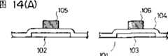
正如图14(A)和15(A)所示,基片101由7059康宁玻璃制成。形成厚度为50nm的大致为本征非晶或多晶半导体膜,例如为非晶硅膜。对该膜绘制为形成n-沟道TFT区102和p-沟道TFT区103的独立区图样。将叠层制品置于氮室内经历60小时温度600℃的热处理,以使TFT各区再结晶。As shown in FIGS. 14(A) and 15(A), the
用ECR PCVD法淀积氧化硅作为115nm厚的栅绝缘膜104。若在这样形成的硅氧化膜中存在象钠离子之类的可动离子,则最好通过将诸如磷之类的元素导入该膜而固定可动离子,以免除可动离子的有害影响。这类元件可通过象等离子掺杂等已知离子掺杂法导入。Silicon oxide was deposited as the
本发明人已发现:用离子掺杂法将磷引入硅氧化膜有效地起到了作为钠吸收剂的作用。在该离子掺杂工序期间,磷离子在2到30KeV,例如10Kev被加速。待掺杂的耙周围压力为2×10⁻⁵至5×10⁻⁴乇,例如为1×10⁻⁴乇。在本例中,耙为氧化硅膜。磷的浓度为5×10¹³至1×10¹⁵离子/cm2,例如为2×1014离子/cm2。这样,磷的剂量小于当形成通常MOS晶体管的掺杂区时所加入的掺杂剂剂量。The present inventors have found that the introduction of phosphorus into the silicon oxide film by ion doping effectively functions as a sodium absorber. During the ion doping process, phosphorus ions are accelerated at 2 to 30 KeV, eg 10 KeV. The pressure around the target to be doped is 2×10⁻⁵ to 5×10⁻⁴ Torr, for example, 1×10⁻⁴ Torr. In this example, the target is a silicon oxide film. The concentration of phosphorus is 5×10¹³ to 1×10¹⁵ ions/cm2 , for example, 2×10¹⁴ ions/cm2 . Thus, the dose of phosphorus is smaller than the dopant dose added when forming the doped region of a conventional MOS transistor.
在这样加入磷之后,将叠层置于氮环境内,经24小时的600℃热处理,以除去因离子掺杂所产生的硅氧化膜中的缺陷。将磷引入硅氧化膜大大地制止了由于可移动离子所造成的性能方面的恶化。因此,可靠性可得以改善。例如,将具有用上述方法形成的硅氧化膜的MOS电容器在经受1小时温度150℃和电压为±20V的偏压/温度处理后,其阈值电压仅变化了1V。在未引入磷的情况下,该阈值电压变化可高达10V以上。After thus adding phosphorus, the laminate was placed in a nitrogen atmosphere and subjected to heat treatment at 600°C for 24 hours to remove defects in the silicon oxide film due to ion doping. The introduction of phosphorus into the silicon oxide film greatly suppresses the deterioration in performance due to mobile ions. Therefore, reliability can be improved. For example, when a MOS capacitor having a silicon oxide film formed by the above method was subjected to a bias/temperature treatment at a temperature of 150°C and a voltage of ±20V for 1 hour, the threshold voltage changed by only 1V. In the absence of phosphorus introduction, the threshold voltage variation can be as high as more than 10V.
在以此方式形成硅氧化膜之后,形成厚度为500nm的耐高温金属的钽膜。对该钽膜绘制图样,以形成n-沟道TFT的栅极部分105和p-沟道TFT的栅极部分106。也可不用钽,代之以低电阻率,即,充分掺杂的多晶硅。此时,沟道长度和宽度均为8μm。栅极及其互连部分均被电气连接到如图15(A)中所示的公共互连部150。After the silicon oxide film was formed in this way, a tantalum film of a refractory metal was formed to a thickness of 500 nm. This tantalum film was patterned to form a
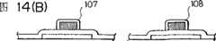
对栅极及其互连部105和106通以电流,以借助阳极化(阳极氧化)法在栅极及其互连部105和106的上表面和侧面上形成铝氧化物膜107和108。除了最大电压为50V之外,与例2中同样实施该阳极化。结果,在这步所制得的阳极化膜的厚度大约为60nm(图14B)。Current is passed through the gate electrode and its
参照图15(B),用激光刻蚀法在151点切割,以使栅极及其互连部105与公共互连部150断开。在此情况下,对互连部150通以电流再次开始阳极化(阳极氧化),以将栅极的阳极氧化表面部分连接到切割后的互连部150。这些条件除了最大电压增至250V外,均与前述条件相同。由于无电流流过互连部105,未观测到任何变化。然而,由于电流流过互连部106(图14c),在栅极互连部106周围形成了厚度约为300nm的钽氧化膜109。Referring to FIG. 15(B), laser etching is used to cut at point 151 so that the gate and its
接着,用离子掺杂法将掺杂剂离子引入半导体102和103的各独立区。用众所周知的CMOS制造技术分别将磷(P)和硼(B)植入半导体区102和103。掺杂离子的能量为80Kev、本发明人和其它人都知道掺杂剂以穿过栅绝缘膜100至300nm厚度的方式被植入,若离子能量超过100Kev,则该处半导体晶粒将因该植入离子的能量而遭到严重破坏。为活化掺杂剂在其内扩散的这些区,必需600℃以上的高温。在此过程中要获得高生产率是极其困难的。然而,在植入离子能量为100KeV或更小处,在600℃以下温度,例如450~500℃即可使电阻足够低。Next, dopant ions are introduced into individual regions of
在离子掺杂步骤之后,将叠层制品置氮室内经历30小时的500℃热处理,以使源区和漏区的表面电阻可达足够低。达到这点时的状态示于图14(D)中。由该图可见,左侧TFT的偏移区之宽度小,而右侧TFT的偏移区之宽度大。此后,用众所周知的技术,在如152和153等的所需位置切割金属互连部106和150。然后,形成层间绝缘膜。形成接触孔。将诸如112和113的导电互连部连接到各电极,从而完成如图15(C)所示电路。After the ion doping step, the laminated product is placed in a nitrogen chamber to undergo heat treatment at 500°C for 30 hours, so that the surface resistance of the source region and the drain region can be sufficiently low. The state when this point is reached is shown in Fig. 14(D). It can be seen from this figure that the width of the offset region of the left TFT is small, and the width of the offset region of the right TFT is large. Thereafter,
在用此法制成的电路中,n-沟道TFT的偏移区宽度小,截止电流稍大,但这种TFT在操作速度方面,性能极好。另一方面,使p-沟道在高速下操作是困难的,但其截止电流小。再者,p-沟道TFT在保持同其源区和漏区之一连接的象素电容器中所储存电荷的能力是极好的。象素电容器包括一对电极(铟锡氧化物)以及设置在电极之间并包括液晶的电光调制层。In the circuit fabricated by this method, the offset region width of the n-channel TFT is small, and the off current is slightly large, but this TFT is excellent in operation speed. On the other hand, it is difficult to make the p-channel operate at high speed, but its off-current is small. Furthermore, p-channel TFTs are excellent in their ability to maintain charges stored in pixel capacitors connected to one of their source and drain regions. A pixel capacitor includes a pair of electrodes (indium tin oxide) and an electro-optic modulation layer disposed between the electrodes and including liquid crystal.
在有些其他情况中,必须将具有不同功能的几个TFT组合地装在一个基片上。例如,在一液晶显示驱动器中,包括移位寄存器的逻辑电路需要高速TFT,而输出电路需要耐高压的TFT。本例的方法在制造必须满足这类矛盾要求的TFT时是切实可行的。实例4In some other cases, it is necessary to mount several TFTs having different functions in combination on one substrate. For example, in a liquid crystal display driver, a logic circuit including a shift register requires a high-speed TFT, and an output circuit requires a high-voltage-resistant TFT. The method of this example is practical in the manufacture of TFTs which must satisfy such contradictory requirements. Example 4
在根据本发明所制造的TFT中,每个偏移区的宽度不仅影响截止电流,而且影响源和漏极之间的耐压性能及操作速度。因此,制作满足这一目的的TFT可通过使诸如阳极化薄膜的厚度之类的某个参数最佳化来实现。然而,通常,调整在一基片上独立形成的各个TFT的这类参数是不可能的。例如,某特定电路需要在同一基片上形成低速操作并耐受高压的TFT和高速操作并耐低压的TFT。根据本发明的基本原理,随着每个偏移区的宽度增大,截止电流减小和电阻对电压特性改善,但操作速度减小。In the TFT manufactured according to the present invention, the width of each offset region affects not only off-current but also the withstand voltage performance between the source and the drain and the operation speed. Therefore, fabricating a TFT satisfying this purpose can be achieved by optimizing a certain parameter such as the thickness of an anodized film. In general, however, it is impossible to adjust such parameters of individual TFTs independently formed on a substrate. For example, a certain circuit needs to form a TFT that operates at a low speed and withstands a high voltage and a TFT that operates at a high speed and withstands a low voltage on the same substrate. According to the basic principle of the present invention, as the width of each offset region increases, off-current decreases and resistance-to-voltage characteristics improve, but the operating speed decreases.
本例解决了这一问题,下面参照图14(A)至14(D)的截面图和图15(A)至15(C)的平面图加以描述。本例关于制造一种图象显示方法中所用的电路,该方法系用一个p-沟道TFT和一个n-沟道TFT去激励一象素,如日本专利申请296331/1991中所述,要求该n沟道TFT以高速操作,但只需承受低电压即可,另一方面,该p-沟道TFT无需以很高速度操作,但其截止电流必须要低。在某些情况下,p-沟道TFT必需承受高电压。因此,就要求:n-沟道TFT的阳极化膜要薄(20至100nm),而p-沟道TFT的阳极化膜要厚(250至400nm)。下面描述本例的制造步骤。This example solves this problem and will be described below with reference to the sectional views of FIGS. 14(A) to 14(D) and the plan views of FIGS. 15(A) to 15(C). This example is concerned with the manufacture of a circuit used in a method of image display for driving a pixel with a p-channel TFT and an n-channel TFT, as described in Japanese Patent Application 296331/1991, requiring The n-channel TFT operates at high speed but only needs to withstand a low voltage, on the other hand, the p-channel TFT does not need to operate at a very high speed, but its off-state current must be low. In some cases, p-channel TFTs must withstand high voltages. Therefore, it is required that the anodized film of the n-channel TFT be thin (20 to 100 nm), and that of the p-channel TFT be thick (250 to 400 nm). The manufacturing steps of this example are described below.
正如图14(A)和15(A)所示,基片101由7059康宁玻璃制成。形成厚度为50nm的大致为本征非晶或多晶半导体膜,例如为非晶硅膜。对该膜绘制为形成n-沟道TFT区102和p-沟道TFT区103的独立区图样。将叠层制品置于氮室内经历60小时温度600℃的热处理,以使TFT各区再结晶。用ECR PCVD法淀积硅氧化物作为115nm厚的栅绝缘膜104。再形成厚度为500nm的耐高温金属的钽膜。对该钽膜绘制图样,以形成n-沟道TFT的栅极部分105和p-沟道TFT的栅极部分106。也可不用钽,代之以低电阻率,即,充分掺杂的多晶硅。此时,沟道长度和宽度均为8μm。栅极及其互连部分均被电气连接到如图15(A)中所示的公共互连部150。As shown in FIGS. 14(A) and 15(A), the
对栅极及其互连部105和106通以电流,以借助阳极化(阳极氧化)法在栅极及其互连部105和106的上表面和侧面上形成铝氧化物膜107和108。除了最大电压为50V之外,与例2同样实施该阳极化。结果,在这步所制得的阳极化膜的厚度大约为60nm(图14B)。Current is passed through the gate electrode and its
参照图15(B),用激光刻蚀法在151点切割,以使栅极及其互连部105与公共互连部150断开。在此情况下,再次开始阳极化,这些条件除了最大电压增至250V外,均与前述条件相同。由于无电流流过互连部105,未观测到任何变化。然而,由于电流流过互连部106(图14c),在栅极互连部106周围形成了厚度约为300nm的钽氧化膜109。Referring to FIG. 15(B), laser etching is used to cut at point 151 so that the gate and its
接着,用离子掺杂法将掺杂剂离子引入半导体102和103的各独立区。用众所周知的CMOS制造技术分别将磷(P)和硼(B)植入半导体区102和103。掺杂离子的能量为80Kev。我们知道若离子能量超过100Kev,为活化掺杂剂在其内扩散的这些区,必需600℃以上的高温。在此过程中要获得高生产率是极其困难的。然而,在植入离子能量小于100Kev处,在600℃以下温度,例如450~500℃,即可使电阻足够低。Next, dopant ions are introduced into individual regions of
在离子掺杂步骤之后,将叠层制品置氮室内经历30小时的500℃热处理,以使源区和漏区的表面电阻可达足够低。达到这点时的状态表示于图14(D)中。由该图可见,左侧TFT的偏移区之宽度小,而右侧TFT的偏移区之宽度大。此后,用众所周知的技术,在如152和153等的所需位置切割金属互连部106和150。然后,形成层间绝缘膜。形成接触孔。将诸如112和113的导电互连部连接到各电极,从而完成如图15(C)所示电路。After the ion doping step, the laminated product is placed in a nitrogen chamber to undergo heat treatment at 500°C for 30 hours, so that the surface resistance of the source region and the drain region can be sufficiently low. The state when this point is reached is shown in Fig. 14(D). It can be seen from this figure that the width of the offset region of the left TFT is small, and the width of the offset region of the right TFT is large. Thereafter,
在用此法制成的电路中,n-沟道TFT的偏移区宽度小,截止电流相对较大,但这种TFT在操作速度方面,性能极好。另一方面,使p-沟道在高速下操作是困难的,但其截止电流小。再者,p-沟道TFT在保持象素电容器中所储存电荷的能力方面是极好的。实例5In the circuit fabricated by this method, the offset region width of the n-channel TFT is small and the off current is relatively large, but this TFT is excellent in operation speed. On the other hand, it is difficult to make the p-channel operate at high speed, but its off-current is small. Also, p-channel TFTs are excellent in the ability to hold charges stored in pixel capacitors. Example 5
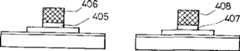
图18(A)至18(D)示出了本例的截面图。基片501由康宁7059玻璃制成。用溅射法形成厚度为100nm的基底硅氧化膜502。再用等离子加速CVD法形成厚度为50nm的非晶硅膜503。为保护非晶硅膜,再用溅射法形成厚度为20nm的硅氧化膜504。将该叠层置于氮环境内,在600℃下经历72小时的热处理,以使这些膜再结晶。再结晶后的薄膜经光学平板印刷法和活性离子刻蚀法(RIE)被绘成图样,以形成半导体岛区,如图18(A)所示。然后,采用氟化氢和氟化氨的混合溶液,即,缓冲的氟氢酸,经湿蚀法除去硅氧化保护膜504。该氟氢酸溶液的一例是由用于半导体制造的1份重量的高纯度氟氢酸(重量为50%)和10份重量的半导体制造用氟化氨(40%)重量组成。该缓冲氟氢酸以70nm/min的速率蚀刻氧化硅,以60nm/min的速率蚀刻硅,和以15nm/min速率蚀刻铝。18(A) to 18(D) show cross-sectional views of this example. Substrate 501 is made of Corning 7059 glass. A base silicon oxide film 502 is formed to a thickness of 100 nm by sputtering. Then, an amorphous silicon film 503 with a thickness of 50 nm was formed by plasma accelerated CVD. In order to protect the amorphous silicon film, a silicon oxide film 504 with a thickness of 20 nm is formed by sputtering. The stack was subjected to a heat treatment at 600° C. for 72 hours in a nitrogen atmosphere to recrystallize the films. The recrystallized film is patterned by optical lithography and reactive ion etching (RIE) to form semiconductor island regions, as shown in FIG. 18(A). Then, the silicon oxide protective film 504 is removed by wet etching using a mixed solution of hydrogen fluoride and ammonium fluoride, that is, buffered hydrofluoric acid. An example of the hydrofluoric acid solution is composed of 1 part by weight of high-purity hydrofluoric acid (50% by weight) for semiconductor manufacture and 10 parts by weight of ammonium fluoride (40%) for semiconductor manufacture. The buffered hydrofluoric acid etches silicon oxide at a rate of 70 nm/min, silicon at a rate of 60 nm/min, and aluminum at a rate of 15 nm/min.
用氧化硅作为耙在氧气环境下经溅射形成厚度为115nm的栅氧化膜505。在此状态下,借助其离子掺杂法将磷离子植入栅氧化膜505,以吸收存在于栅氧化膜内部诸如钠之类的可移动离子。在钠离子浓度低以致器件的工作不受可移动离子阻碍的场合,无需进行离子植入。在本例中,等离子加速电压为10Kev。剂量为2×10¹⁴离子/cm2。将叠层置于600℃进行24小时热处理。这样,由等离子掺杂的过程中的碰撞引起对氧化膜和对硅膜的损害得以恢复。A
然后,用溅射法形成铝膜并用混合酸,即,添加了5%硝酸的磷酸溶液,绘制图样以形成栅极及其互连部506。当刻蚀温度为40℃时刻蚀率为225nm/min。以此方式调整TFT的外形。此时,沟道长度为8μm,宽度为20μm。Then, an aluminum film was formed by sputtering and patterned with a mixed acid, ie, a phosphoric acid solution to which 5% nitric acid was added, to form gate electrodes and their
N型掺杂区507或说源区和漏区,用离子植入法形成于半导体区中。在这一步,磷离子作为掺杂剂离子被植入。离子能量为80Kev,剂量为5×10¹⁵离子/cm2。如图所示,掺杂剂离子是穿过氧化膜而植入的。采用这种植入法的优点在于:在利用激光热处理而连续再结晶期间,保持了掺杂区表面的平滑度。在不采用这种植入的情况下,则在结晶期间,大量的晶核形成在掺杂区的表面上,从而引起该表面的不平整。这样,导出图18(B)所示结构。当然,经过这一离子植入工序,掺杂部分的结晶度受到严重破坏。这些部分大致呈现非晶态或接近于非晶态的多晶态。The N-type doped
对互连部506通以电流。经阳极化在栅极及其互连部的顶部表面和侧面形成铝氧化膜508。就这阳极化而言,将3%的酒石酸的乙二醇溶液用5%氨中和,以将该溶液的PH值调到7.0±0.2。将铂作为阴极浸入该溶液。然后,将TFT连同该基片一起浸入该溶液。将互连部506连接至电源的阳极。将温度保持在25±2℃。A current is passed through the
在这种情况下,先通以0.5mA/cm2的电流。当电压达到200V时,保持该电压不变,则器件被供电。当电流达到0.005mA/cm2时,切断电流,从而结束阳极化工序。这样获得的阳极化膜(栅极的阳极氧化涂层)的厚度约为250nm。见图18(c)所示。In this case, a current of 0.5 mA/cm2 was passed first. When the voltage reaches 200V, keep the voltage constant, and the device is powered. When the current reaches 0.005 mA/cm2 , the current is cut off, thereby ending the anodizing process. The thickness of the anodized film thus obtained (anodized coating of the gate electrode) was about 250 nm. See Figure 18(c).
接着用KrF作激发物的激光器对叠层进行激光热处理。例如,发出功率密度为350mJ/cm2的10个冲击(shots)激光脉冲。我们已肯定:可将非晶硅的结晶度恢复到如此程度,以致非晶硅可经得住由至少一个冲击激光辐照所引起的TFT的操作。为了最大限度地降低由于激光器功率波动而引起缺陷的可能性,需要足够数量的激光器脉冲的冲击。不过,过多的激光辐照冲击将使生产率下降。我们已发现:本例所用的10个冲击激光脉冲是最理想的。Next, laser heat treatment is performed on the laminate with a laser using KrF as the exciter. For example, 10 shots of laser pulses with a power density of 350 mJ/cm2 are emitted. We have determined that the crystallinity of amorphous silicon can be restored to such an extent that amorphous silicon can withstand operation of TFTs induced by at least one shock laser irradiation. To minimize the possibility of defects being induced due to laser power fluctuations, a shock of a sufficient number of laser pulses is required. However, excessive laser irradiation shock will reduce productivity. We have found that the 10 shock laser pulses used in this example are optimal.
为提高生产率,激光热处理是在大气中进行的。由于硅氧化膜已形成在掺杂区上,未发生问题。在暴露掺杂区而进行激光热处理的场合,在结晶化的同时,将大气中的氧带入了掺杂区,固而使结晶性变坏。这样,便不能获得具备令人满意性能的TFT。因此,对暴露掺杂区的叠层要求其应在真空中进行激光热处理。To increase productivity, laser heat treatment is performed in the atmosphere. Since the silicon oxide film had been formed on the doped region, no problem occurred. When laser heat treatment is performed by exposing the doped region, oxygen in the atmosphere is brought into the doped region at the same time as crystallization, so that the crystallinity deteriorates. Thus, a TFT with satisfactory performance cannot be obtained. Therefore, it is required that the stack of exposed doped regions should be laser annealed in vacuum.
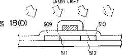
本例中,如图18(D)所示,所进行的激光辐照是斜向进入叠层的。例如,激光辐射角与基片法向成10°角。该角度按照该制成器件的设计说明书确定。对掺杂区而言,由激光结晶的区域可为非对称的。也就是说,区域509和510是经充分结晶后的掺杂区。区域511不是掺杂区,但已经激光辐照而结晶化。区域512是掺杂区但不是结晶区。例如,图18(D)右侧上的掺杂区可用作势必产生热电子的漏区。In this example, as shown in Fig. 18(D), laser irradiation was performed obliquely into the stack. For example, the laser radiation angle is 10° from the substrate normal. The angle is determined according to the design specification of the fabricated device. For doped regions, the region crystallized by the laser may be asymmetric. That is,
由此可见,器件的形状得到了调整。此后,用传统方法溅射硅氧化物,以形成层间绝缘。用众所周知的光学平板印刷术形成电极孔,以暴露半导体区的表面或栅极及其互连部表面。最后,有选择地形成金属涂层。这样,便制成一个器件。实施6It can be seen that the shape of the device has been adjusted. Thereafter, silicon oxide is sputtered by conventional methods to form interlayer insulation. Electrode holes are formed by well-known optical lithography to expose the surface of the semiconductor region or the surface of the gate and its interconnections. Finally, a metal coating is optionally formed. Thus, a device is produced.
在根据本发明所制作的TFT中,非晶半导体区的宽度和每个偏移区的宽度不仅影响截止电流而且影响漏和源区之间的耐压能力及操作速度。因此,通过使象阳极化膜的厚度或植入离子的能量之类参数的量佳化便可制得满足目标的TFT。然而,通常对独立形成于一个基片上的各个TFT调整这类参数是不可能的。例如,一个实际电路需要在同一基片上形成低速操作并耐高压的TFT和高速操作并承受低压的TFT。根据本发明的基本原理,随着每个偏移区的宽度或掺杂非晶半导体区的宽度增大,截止电流减小并且电阻-电压特性得到改善,但操作速度降低。In the TFT manufactured according to the present invention, the width of the amorphous semiconductor region and the width of each offset region affect not only the off current but also the withstand voltage capability between the drain and source regions and the operation speed. Therefore, by optimizing the amount of parameters such as the thickness of the anodized film or the energy of implanted ions, a TFT satisfying the target can be produced. However, it is generally not possible to adjust such parameters for individual TFTs independently formed on a substrate. For example, an actual circuit needs to form a TFT operating at a low speed and withstanding a high voltage and a TFT operating at a high speed and withstanding a low voltage on the same substrate. According to the basic principle of the present invention, as the width of each offset region or the width of the doped amorphous semiconductor region increases, off-current decreases and resistance-voltage characteristics improve, but the operation speed decreases.
本例解决了这一问题,下面参照图22(A)至22(C)的平面图和图19(A)至19(D)的截面图加以描述。本例属于制造一种图象显示法中所用的电路,如日本专利申请296331/1991中所述,该方法采用一个p-沟道TFT和一个n-沟道TFT去激励一象素。该n-沟道TFT需以高速操作,但只需承受低电压即可。另一方面,p-沟道TFT无需高速操作,但要求其截止电流必需很低。在某些情况下,p-沟道TFT必需承受高电压。因此,就要求n-沟道TFT的阳极化膜要薄(20至100nm),而p沟道TFT的阳极化膜要厚(250至400nm)。下面描述本例的制造步骤。This example solves this problem and will be described below with reference to the plan views of FIGS. 22(A) to 22(C) and the sectional views of FIGS. 19(A) to 19(D). This example pertains to the manufacture of a circuit used in an image display method, as described in Japanese Patent Application No. 296331/1991, which uses a p-channel TFT and an n-channel TFT to drive a pixel. The n-channel TFT needs to operate at high speed, but only needs to withstand low voltage. On the other hand, a p-channel TFT does not require high-speed operation, but its off-current must be low. In some cases, p-channel TFTs must withstand high voltages. Therefore, it is required that the anodized film of the n-channel TFT be thin (20 to 100 nm), and that of the p-channel TFT be thick (250 to 400 nm). The manufacturing steps of this example are described below.
与例5中一样,基片601由康宁7059玻璃制成。形成一n型掺杂区602,p-型掺杂区603,栅极绝缘膜604,栅极606及其互连体607。栅极606及其互连体607连到互联部650(图22(A)和19(A))。As in Example 5, the substrate 601 was made of Corning 7059 glass. An n-type doped region 602, a p-type doped region 603, a gate insulating film 604, a gate 606 and its interconnection 607 are formed. The gate electrode 606 and its interconnection 607 are connected to an interconnection 650 (FIGS. 22(A) and 19(A)).
栅极606及其互连体607被通以电流。用阳极化法,形成栅极606及其互连体607的顶部和侧表面上的铝氧化膜613和614。阳极化步骤除最大电压为50V外,与实例5一样进行。在这步中所制得的阳极化膜的厚度约为60nm(图19(B))。The gate 606 and its interconnect 607 are passed with current. Aluminum oxide films 613 and 614 are formed on the top and side surfaces of the gate electrode 606 and its interconnector 607 by anodization. The anodizing step was performed as in Example 5 except that the maximum voltage was 50V. The thickness of the anodized film produced in this step was about 60 nm (Fig. 19(B)).
现参照图22(B),用激光刻蚀法从互连体650的651处切开使其与栅极及其互连体606分割开。在此情况下,再次开始阳极化,阳极化步骤的条件除最大电压增为250V外,与先前条件一样。由于没有电流流过互连体606,故未观测到任何变化。但,由于电流流过互连体607(图19(c)),故在栅极互连体607周围形成了厚度为300nm左右的铝氧化膜615。Referring now to FIG. 22(B), the interconnection 650 is cut at 651 by laser etching to separate it from the gate and its interconnection 606 . In this case, anodization was started again, and the conditions of the anodization step were the same as the previous conditions except that the maximum voltage was increased to 250V. Since no current flows through interconnect 606, no change is observed. However, since the current flows through the interconnector 607 ( FIG. 19( c )), an aluminum oxide film 615 with a thickness of about 300 nm is formed around the gate interconnector 607 .
然后,在与例5相同条件下,进行叠层的激光热处理。在此情况下,就n-沟道TFT而言,(图19(A)-(D)的左侧),非晶区和偏移区的宽度a1是如此之窄,因此可忽略不计。在铝互连体的表面未涂敷阳极化膜的地方,互连体因激光照射而严重损坏。因此,有必要形成阳极化膜,尽管它不厚。另一方面,就p-沟道TFT而言,(在图19的右侧)阳极化膜的厚度为300nm。还存在厚度为150至200nm的非晶区。偏移区的宽度a2估计应为100至150nm(图19(D))。Then, under the same conditions as in Example 5, laser heat treatment of the laminate was performed. In this case, in the case of n-channel TFT, (the left side of FIG. 19(A)-(D)), the widtha1 of the amorphous region and the offset region is so narrow that it can be ignored. Where the surface of the aluminum interconnect is not coated with an anodized film, the interconnect is severely damaged by laser irradiation. Therefore, it is necessary to form an anodized film although it is not thick. On the other hand, in the case of a p-channel TFT, (on the right side of FIG. 19 ) the thickness of the anodized film was 300 nm. There is also an amorphous region with a thickness of 150 to 200 nm. The widtha2 of the offset region is estimated to be 100 to 150 nm (FIG. 19(D)).
与图5中一样,在大气下经激光器辐照,在所需位置上刻蚀铝互连体。使p-沟道TFT的栅极与互连体607分开。互连体650也被切割。形成一层间绝缘膜。形成接触孔,形成互连体624和611。这样,便形成了一个电路。As in FIG. 5, the aluminum interconnect is etched at the desired position by laser irradiation under the atmosphere. The gate of the p-channel TFT is separated from the interconnect 607 . Interconnects 650 are also cut. An interlayer insulating film is formed. Contact holes are formed to form
在这样制成的电路中,n-沟道TFT的偏移区和非晶区都窄。虽然截止电流略大,但操作速度极佳。另一方面,欲p沟道TFT在高速下工作是困难的。不过截止电流是小的。在保持储存于象素电容器内的电荷方面的性能极好。In the thus fabricated circuit, both the offset region and the amorphous region of the n-channel TFT are narrow. Although the cutoff current is slightly larger, the operating speed is excellent. On the other hand, it is difficult to operate a p-channel TFT at high speed. However, the cut-off current is small. Excellent performance in maintaining the charge stored in the pixel capacitor.
还存在具有不同功能的TFT必需组合安装在同一基片上的其它情况。例如,在一液晶显示驱动器里,包含移位寄存器的逻辑电路需要高速TFT,而输出电路需要耐高压的TFT。本例的方法可有效地用于制造必需满足这类矛盾要求的TFT。实例7There are other cases where TFTs having different functions must be mounted in combination on the same substrate. For example, in a liquid crystal display driver, the logic circuit including the shift register needs a high-speed TFT, and the output circuit needs a high-voltage-resistant TFT. The method of this example can be effectively used to manufacture TFTs which must satisfy such contradictory requirements. Example 7
借助例1所用方法所制造的由n-沟道TFT组成的一个有源矩阵电路示于图20中。该有源矩阵包括选通线701和数据线702,分别排列成行和列。这些线由低电阻率的铝构成并涂敷以厚度为200至400nm的铝氧化膜——因该电路经历了根据本发明的阳极化步骤。这些线的宽度为2μm。这些线的厚度为0.5μm。用于象素的TFT的栅极703同选通线701连接。栅极也涂敷有氧化铝。在栅极下面形成了半导体层704。与例1的n-沟道TFT一样,也存在掺杂有磷的n型多晶区。至于构成本发明特点之一的偏移区,其宽度设为200至400nm左右。该半导体层的源同数据线702处于接触中。诸漏区经由铝极705同由ITO构成的象素电极706连接。An active matrix circuit composed of n-channel TFTs fabricated by the method used in Example 1 is shown in FIG. 20 . The active matrix includes gate lines 701 and data lines 702 arranged in rows and columns, respectively. These lines consist of aluminum with low resistivity and are coated with an aluminum oxide film with a thickness of 200 to 400 nm—since the circuit has undergone the anodization step according to the invention. The width of these lines is 2 μm. The thickness of these lines is 0.5 μm. A gate 703 of a TFT for a pixel is connected to a gate line 701 . The gate is also coated with aluminum oxide. A semiconductor layer 704 is formed under the gate. As with the n-channel TFT of Example 1, there is also an n-type polycrystalline region doped with phosphorus. As for the offset region constituting one of the features of the present invention, its width is set at about 200 to 400 nm. The source of the semiconductor layer is in contact with the data line 702 . The drain regions are connected to a pixel electrode 706 made of ITO via an aluminum electrode 705 .
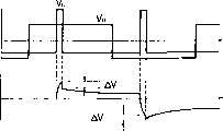
图21为按本例所制作的一个有源矩阵装置的电路原理图。图21(A)示出该装置的操作情况。图21(B)示出一个包含用先有技术方法制作的TFT的装置操作情况,以供对照用。正如先前所述,在这种结构的矩阵电路中,人们已知:当电容器C的充电结束和栅压中断时,则电容器C经由栅和漏极间的寄生电容C被容性地耦合到选通线。该电压比充电电压减小了V。这种现象从并联连接的n-沟道TFT的电路中也可观测到。这方面情况在由本申请人提交的专利申请208648/1991中作了详述。Fig. 21 is a schematic circuit diagram of an active matrix device fabricated according to this example. Fig. 21(A) shows the operation of the device. Figure 21(B) shows the operation of a device comprising a TFT fabricated by the prior art method for comparison. As mentioned earlier, in the matrix circuit of this structure, it is known that when the charging of the capacitor C ends and the gate voltage is interrupted, the capacitor C is capacitively coupled to the selected capacitor via the parasitic capacitance C between the gate and the drain. pass line. This voltage is reduced by V from the charging voltage. This phenomenon is also observed from a circuit in which n-channel TFTs are connected in parallel. This aspect is described in detail in patent application 208648/1991 filed by the applicant.
正如图21所示,在仅由一个TFT,即,或一个n-沟道TFT,或一个P-沟道TFT构成的电路中,该电压降由下式给定As shown in Fig. 21, in a circuit composed of only one TFT, i.e., either an n-channel TFT, or a p-channel TFT, the voltage drop is given by
V=CGDVG1(CLC+CGD)式中VG为栅压的接通电压与截止电压之差。例如,在一个未采用自调整工序制成的TFT中,寄生电容CGD相当大,故电压降V也大。为解决这一问题,正如图21所示,将存储电容器CAD同象素电容器并联,以增大象素电容器的视在电容量。然而,该方法未根本解决该问题。正如已经说过的:引起了诸如孔径减小之类的新问题。V=CGD VG 1(CLC +CGD ) In the formula, VG is the difference between the turn-on voltage and the cut-off voltage of the gate voltage. For example, in a TFT fabricated without a self-adjustment process, the parasitic capacitance CGD is relatively large, so the voltage drop V is also large. To solve this problem, as shown in FIG. 21, a storage capacitor CAD is connected in parallel with the pixel capacitor to increase the apparent capacitance of the pixel capacitor. However, this method does not fundamentally solve the problem. As already said: new problems such as pore size reduction arise.
即使对采用自调整工艺制得的器件而言,若象素尺寸非常之小,以致同象素电容相比已不能忽略TFT的寄生电容影响时,则这个电压降会引起严重问题。例如,在一个配合高分辨率电视投影用的对角线为3英寸的投影屏中,象素电容小到13fF。另一方面,在由采用2μm规则的工艺制造TFT的场合,互连体的纵横比大。因此,即使不存在重叠,在三维几何空间内也会产生寄生电容。该电容达到几个5F,即是象素电容量的10%或更大。Even for devices made using a self-regulating process, this voltage drop can cause serious problems if the pixel size is so small that the effect of the parasitic capacitance of the TFT is no longer negligible compared to the pixel capacitance. For example, in a projection screen with a diagonal of 3 inches for high-resolution television projection, the pixel capacitance is as small as 13 fF. On the other hand, in the case of manufacturing TFTs by a process employing a 2 µm rule, the aspect ratio of the interconnector is large. Therefore, even in the absence of overlap, parasitic capacitance occurs in the three-dimensional geometric space. This capacitance amounts to several 5F, ie, 10% or more of the pixel capacitance.
采用传统式TFT的有源矩阵电路示于图21(A)中。显然,要形成正确的显示受到电压降V的不良影响。具体地说,为了使TFT高速操作,必需使栅极高于漏压。通常,使栅极大约两倍于所用漏压。因此若漏电压是5V,则栅压为10V或更高。在为完善TFT的操作而使栅压在截止态时为负的场合,栅压呈更大程度的变化。在图21的情况下,漏压为±6V的交流。栅压在接通态时为+12V,截止态时为-4V。根据上述方程,我们可求得VG=16V。正如图21(A)所示,若寄生电容为2fF,则电压降V为2V。这正好为1/3的漏极充电电压。当然,贮存于象素中的电荷通过自然放电而释放,因此,实际上要提供理想的显示是极其困难的。为避免这一问题,务必牺牲孔经比(aperture ratio)来设置存储电容器。An active matrix circuit using conventional TFTs is shown in Fig. 21(A). Obviously, forming a correct display is adversely affected by the voltage drop V. Specifically, in order to operate a TFT at a high speed, it is necessary to make the gate higher than the drain voltage. Typically, make the gate approximately twice the drain voltage used. So if the drain voltage is 5V, the gate voltage is 10V or higher. Where the gate voltage is negative in the off state for perfect TFT operation, the gate voltage varies to a greater extent. In the case of FIG. 21, the leakage voltage is AC of ±6V. The gate voltage is +12V in the on state and -4V in the off state. According to the above equation, we can obtain VG =16V. As shown in FIG. 21(A), if the parasitic capacitance is 2fF, the voltage drop V is 2V. This is exactly 1/3 the drain charging voltage. Of course, the charges stored in the pixels are released by natural discharge, and therefore, it is extremely difficult to provide an ideal display in practice. To avoid this problem, the storage capacitor must be set at a sacrifice of aperture ratio.
另一方面,根据本发明可大大减小寄生电容量。更准确地说,该电容可降至0.1fF以下。因此,如图21(B)所示,该电压降V几乎可忽略不计。此外,根据本发明方法的器件截止电流比用先有技术方法制成的TFT的截止电流小了大约一个数量级。因此,自发放电要微弱得多,故能提供近乎理想的显示。On the other hand, according to the present invention, the parasitic capacitance can be greatly reduced. More precisely, this capacitance can be reduced to less than 0.1fF. Therefore, as shown in FIG. 21(B), the voltage drop V is almost negligible. Furthermore, the off-current of the device according to the method of the present invention is about an order of magnitude smaller than that of a TFT made by the prior art method. Therefore, the spontaneous discharge is much weaker, so it can provide a nearly ideal display.
由此可见,根据本发明,在栅极表面形成了一绝缘的阳极化层。这样,沟道长度是大于栅极沿沟道纵向所占长度的。因此,在沟道区的相对侧面上形成了偏移区,该偏移区不接收栅极电场或接受栅极的极微弱电场。同样,能形成有相同优点的磷掺杂半导体区。这减小了反向偏置的漏电流。结果:省去了在此之前为维持电荷所必需的电容。在先有技术中约为20%的孔径比可改善到35%以上。因此,可形成较高质量的显示。Thus, according to the present invention, an insulating anodized layer is formed on the surface of the gate. In this way, the length of the channel is greater than the length occupied by the gate along the longitudinal direction of the channel. Therefore, an offset region is formed on the opposite side of the channel region, which does not receive the electric field of the gate or accepts an extremely weak electric field of the gate. Also, a phosphorus-doped semiconductor region can be formed with the same advantages. This reduces reverse bias leakage current. Result: The capacitance previously necessary to maintain the charge is eliminated. The aperture ratio of about 20% in the prior art can be improved to more than 35%. Therefore, a higher quality display can be formed.
根据本发明,偏移区和掺杂非晶半导体区是由栅极的阳极化膜的厚度来确定的。因此,这些区的宽度可精确地控制在10至100nm之间。我们并未觉察到因添加了这一制造步骤而导致生产率的大降。而且不存在可被视为生产率减小的原因的任何因素。According to the present invention, the offset region and the doped amorphous semiconductor region are determined by the thickness of the anodized film of the gate. Therefore, the width of these regions can be precisely controlled between 10 and 100 nm. We did not notice a significant drop in productivity due to the addition of this manufacturing step. And there is not any factor that can be regarded as the cause of the reduction in productivity.
至此,我们主要是以硅半导体器件作为对象加以描述的,但显然,本发明也适于采用锗,碳化硅,砷化镓或其它材料的半导体器件。So far, we have mainly described silicon semiconductor devices as the object, but obviously, the present invention is also applicable to semiconductor devices using germanium, silicon carbide, gallium arsenide or other materials.
Claims (70)
Applications Claiming Priority (15)
| Application Number | Priority Date | Filing Date | Title |
|---|---|---|---|
| JP23710091 | 1991-08-23 | ||
| JP237100/1991 | 1991-08-23 | ||
| JP237100/91 | 1991-08-23 | ||
| JP34033691AJPH05267666A (en) | 1991-08-23 | 1991-11-29 | Semiconductor device and manufacturing method thereof |
| JP340336/91 | 1991-11-29 | ||
| JP340336/1991 | 1991-11-29 | ||
| JP34194/1992 | 1992-01-24 | ||
| JP34194/92 | 1992-01-24 | ||
| JP3419492AJP2845303B2 (en) | 1991-08-23 | 1992-01-24 | Semiconductor device and manufacturing method thereof |
| JP38637/92 | 1992-01-29 | ||
| JP38637/1992 | 1992-01-29 | ||
| JP3863792AJP2585158B2 (en) | 1991-08-23 | 1992-01-29 | Method for manufacturing semiconductor device |
| JP54322/1992 | 1992-02-05 | ||
| JP54322/92 | 1992-02-05 | ||
| JP5432292AJP2540688B2 (en) | 1991-08-23 | 1992-02-05 | Semiconductor device and manufacturing method thereof |
Related Child Applications (3)
| Application Number | Title | Priority Date | Filing Date |
|---|---|---|---|
| CN200410088064.8ADivisionCN1603924B (en) | 1991-08-23 | 1992-08-22 | Active matrix liquid crystal electro-optic device and video camera equipped with the device |
| CN00133102.7ADivisionCN1183599C (en) | 1991-08-23 | 1992-08-22 | Active Matrix Display Devices |
| CN03133133.5ADivisionCN1266519C (en) | 1991-08-23 | 1992-08-22 | Semiclnductor display device and electronic device with the semiconductor display device |
Publications (2)
| Publication Number | Publication Date |
|---|---|
| CN1070052A CN1070052A (en) | 1993-03-17 |
| CN1121741Ctrue CN1121741C (en) | 2003-09-17 |
Family
ID=27521591
Family Applications (4)
| Application Number | Title | Priority Date | Filing Date |
|---|---|---|---|
| CN00133102.7AExpired - LifetimeCN1183599C (en) | 1991-08-23 | 1992-08-22 | Active Matrix Display Devices |
| CN92110004.3AExpired - LifetimeCN1121741C (en) | 1991-08-23 | 1992-08-22 | Semiconductor device and manufacturing method thereof |
| CN200410088064.8AExpired - LifetimeCN1603924B (en) | 1991-08-23 | 1992-08-22 | Active matrix liquid crystal electro-optic device and video camera equipped with the device |
| CN03133133.5AExpired - LifetimeCN1266519C (en) | 1991-08-23 | 1992-08-22 | Semiclnductor display device and electronic device with the semiconductor display device |
Family Applications Before (1)
| Application Number | Title | Priority Date | Filing Date |
|---|---|---|---|
| CN00133102.7AExpired - LifetimeCN1183599C (en) | 1991-08-23 | 1992-08-22 | Active Matrix Display Devices |
Family Applications After (2)
| Application Number | Title | Priority Date | Filing Date |
|---|---|---|---|
| CN200410088064.8AExpired - LifetimeCN1603924B (en) | 1991-08-23 | 1992-08-22 | Active matrix liquid crystal electro-optic device and video camera equipped with the device |
| CN03133133.5AExpired - LifetimeCN1266519C (en) | 1991-08-23 | 1992-08-22 | Semiclnductor display device and electronic device with the semiconductor display device |
Country Status (2)
| Country | Link |
|---|---|
| CN (4) | CN1183599C (en) |
| TW (2) | TW540828U (en) |
Families Citing this family (13)
| Publication number | Priority date | Publication date | Assignee | Title |
|---|---|---|---|---|
| TW297142B (en)* | 1993-09-20 | 1997-02-01 | Handotai Energy Kenkyusho Kk | |
| CN1324388C (en)* | 2003-03-14 | 2007-07-04 | 友达光电股份有限公司 | Manufacturing method of low temperature polysilicon thin film transistor liquid crystal display |
| US7532184B2 (en)* | 2003-04-17 | 2009-05-12 | Samsung Mobile Display Co., Ltd. | Flat panel display with improved white balance |
| KR100569718B1 (en) | 2003-05-20 | 2006-04-10 | 삼성전자주식회사 | Multidomain liquid crystal display |
| US7074657B2 (en)* | 2003-11-14 | 2006-07-11 | Advanced Micro Devices, Inc. | Low-power multiple-channel fully depleted quantum well CMOSFETs |
| US7915058B2 (en) | 2005-01-28 | 2011-03-29 | Semiconductor Energy Laboratory Co., Ltd. | Substrate having pattern and method for manufacturing the same, and semiconductor device and method for manufacturing the same |
| JP5512931B2 (en)* | 2007-03-26 | 2014-06-04 | 株式会社半導体エネルギー研究所 | Method for manufacturing semiconductor device |
| KR101774478B1 (en)* | 2010-10-22 | 2017-09-05 | 삼성디스플레이 주식회사 | Thin film transistor and manufacturing method thereof |
| GB2489682B (en)* | 2011-03-30 | 2015-11-04 | Pragmatic Printing Ltd | Electronic device and its method of manufacture |
| CN102820320B (en) | 2011-06-09 | 2015-03-04 | 中芯国际集成电路制造(北京)有限公司 | Silicon-on-semiinsulator semiconductor device and method for manufacturing same |
| CN106249947B (en) | 2016-07-22 | 2019-04-19 | 京东方科技集团股份有限公司 | A substrate and display device |
| CN108983526B (en)* | 2018-10-22 | 2023-10-13 | 五邑大学 | Current-driven color-changing device and preparation method thereof |
| KR102822240B1 (en)* | 2019-07-30 | 2025-06-20 | 삼성디스플레이 주식회사 | Display device and method of fabricating the same |
Family Cites Families (2)
| Publication number | Priority date | Publication date | Assignee | Title |
|---|---|---|---|---|
| JPS59188974A (en)* | 1983-04-11 | 1984-10-26 | Nec Corp | Manufacturing method of semiconductor device |
| GB2238683A (en)* | 1989-11-29 | 1991-06-05 | Philips Electronic Associated | A thin film transistor circuit |
- 1992
- 1992-07-29TWTW089205194Upatent/TW540828U/ennot_activeIP Right Cessation
- 1992-07-29TWTW087207861Upatent/TW476451U/ennot_activeIP Right Cessation
- 1992-08-22CNCN00133102.7Apatent/CN1183599C/ennot_activeExpired - Lifetime
- 1992-08-22CNCN92110004.3Apatent/CN1121741C/ennot_activeExpired - Lifetime
- 1992-08-22CNCN200410088064.8Apatent/CN1603924B/ennot_activeExpired - Lifetime
- 1992-08-22CNCN03133133.5Apatent/CN1266519C/ennot_activeExpired - Lifetime
Also Published As
| Publication number | Publication date |
|---|---|
| TW476451U (en) | 2002-02-11 |
| CN1603924B (en) | 2011-04-20 |
| CN1266519C (en) | 2006-07-26 |
| CN1183599C (en) | 2005-01-05 |
| CN1479137A (en) | 2004-03-03 |
| CN1603924A (en) | 2005-04-06 |
| CN1070052A (en) | 1993-03-17 |
| TW540828U (en) | 2003-07-01 |
| CN1305227A (en) | 2001-07-25 |
Similar Documents
| Publication | Publication Date | Title |
|---|---|---|
| KR970002004B1 (en) | Semiconductor device and method for forming the same | |
| CN1249818C (en) | Semiconductor device and manufacturing method thereof | |
| US5521107A (en) | Method for forming a field-effect transistor including anodic oxidation of the gate | |
| US5485019A (en) | Semiconductor device and method for forming the same | |
| US8987120B2 (en) | Flat panel display device comprising polysilicon thin film transistor and method of manufacturing the same | |
| JP2585158B2 (en) | Method for manufacturing semiconductor device | |
| CN1092556A (en) | MIS semiconductor device and manufacturing method thereof | |
| CN1121741C (en) | Semiconductor device and manufacturing method thereof | |
| JP2009049388A (en) | Method for manufacturing display device | |
| KR100676330B1 (en) | Semiconductor device, method of manufacturing semiconductor device and method of manufacturing thin film transistor | |
| CN1501437A (en) | Mask for polycrystallization and method of manufacturing thin film transistor using same | |
| CN1487569A (en) | Method for producing thin film transistor | |
| CN1725510A (en) | Low temperature polysilicon thin film transistor and its manufacturing method | |
| JP2540688B2 (en) | Semiconductor device and manufacturing method thereof | |
| JP2868168B2 (en) | Method for manufacturing semiconductor device | |
| JP2890037B2 (en) | Semiconductor device and manufacturing method thereof | |
| KR960008133B1 (en) | Semiconductor device and manufacturing method thereof | |
| CN1133489A (en) | Method for making semiconductor device | |
| KR960011185B1 (en) | Electro-optical device | |
| JP3000213B2 (en) | Semiconductor devices and active matrix liquid crystal display devices. | |
| JP2652366B2 (en) | Semiconductor device and manufacturing method thereof | |
| JP2000068521A (en) | Semiconductor device | |
| JPH0990414A (en) | Liquid crystal display manufacturing method | |
| JPH09166791A (en) | Semiconductor device and active matrix type liquid crystal display device | |
| JP2001166339A (en) | Display device |
Legal Events
| Date | Code | Title | Description |
|---|---|---|---|
| C06 | Publication | ||
| PB01 | Publication | ||
| C10 | Entry into substantive examination | ||
| SE01 | Entry into force of request for substantive examination | ||
| C14 | Grant of patent or utility model | ||
| GR01 | Patent grant | ||
| C17 | Cessation of patent right | ||
| CX01 | Expiry of patent term | Expiration termination date:20120822 Granted publication date:20030917 |