CN112151458A - Functional packaging module and preparation method thereof, functional packaging component and electronic device - Google Patents
Functional packaging module and preparation method thereof, functional packaging component and electronic deviceDownload PDFInfo
- Publication number
- CN112151458A CN112151458ACN202011014037.1ACN202011014037ACN112151458ACN 112151458 ACN112151458 ACN 112151458ACN 202011014037 ACN202011014037 ACN 202011014037ACN 112151458 ACN112151458 ACN 112151458A
- Authority
- CN
- China
- Prior art keywords
- functional device
- functional
- electrical connection
- connection layer
- layer
- Prior art date
- Legal status (The legal status is an assumption and is not a legal conclusion. Google has not performed a legal analysis and makes no representation as to the accuracy of the status listed.)
- Granted
Links
- 238000004806packaging method and processMethods0.000titleclaimsabstractdescription36
- 238000002360preparation methodMethods0.000titleabstractdescription4
- 239000003292glueSubstances0.000claimsabstractdescription32
- 239000002184metalSubstances0.000claimsdescription64
- 238000002955isolationMethods0.000claimsdescription13
- 238000000034methodMethods0.000claimsdescription12
- 238000011049fillingMethods0.000claimsdescription8
- 239000000758substrateSubstances0.000claimsdescription7
- 238000004519manufacturing processMethods0.000claimsdescription5
- XUIMIQQOPSSXEZ-UHFFFAOYSA-NSiliconChemical compound[Si]XUIMIQQOPSSXEZ-UHFFFAOYSA-N0.000claimsdescription4
- 239000000463materialSubstances0.000claimsdescription4
- 229910052710siliconInorganic materials0.000claimsdescription4
- 239000010703siliconSubstances0.000claimsdescription4
- 230000000149penetrating effectEffects0.000claims1
- 239000010410layerSubstances0.000description138
- 238000005538encapsulationMethods0.000description5
- 238000009434installationMethods0.000description4
- 230000005611electricityEffects0.000description3
- 230000008569processEffects0.000description3
- 229910000679solderInorganic materials0.000description3
- 238000003466weldingMethods0.000description3
- 239000002313adhesive filmSubstances0.000description2
- 239000011248coating agentSubstances0.000description2
- 238000000576coating methodMethods0.000description2
- 238000009826distributionMethods0.000description2
- 238000003754machiningMethods0.000description2
- 230000004048modificationEffects0.000description2
- 238000012986modificationMethods0.000description2
- 238000007747platingMethods0.000description2
- 230000003068static effectEffects0.000description2
- 238000004026adhesive bondingMethods0.000description1
- 230000009286beneficial effectEffects0.000description1
- 239000000919ceramicSubstances0.000description1
- 239000011247coating layerSubstances0.000description1
- 230000008094contradictory effectEffects0.000description1
- 238000010586diagramMethods0.000description1
- 230000000694effectsEffects0.000description1
- 238000005516engineering processMethods0.000description1
- 238000005530etchingMethods0.000description1
- 230000006872improvementEffects0.000description1
- 230000001939inductive effectEffects0.000description1
- 238000011900installation processMethods0.000description1
- 239000007769metal materialSubstances0.000description1
- 238000005457optimizationMethods0.000description1
- 230000001681protective effectEffects0.000description1
Images


Classifications
- H—ELECTRICITY
- H01—ELECTRIC ELEMENTS
- H01L—SEMICONDUCTOR DEVICES NOT COVERED BY CLASS H10
- H01L23/00—Details of semiconductor or other solid state devices
- H01L23/12—Mountings, e.g. non-detachable insulating substrates
- H01L23/13—Mountings, e.g. non-detachable insulating substrates characterised by the shape
- H—ELECTRICITY
- H01—ELECTRIC ELEMENTS
- H01L—SEMICONDUCTOR DEVICES NOT COVERED BY CLASS H10
- H01L21/00—Processes or apparatus adapted for the manufacture or treatment of semiconductor or solid state devices or of parts thereof
- H01L21/02—Manufacture or treatment of semiconductor devices or of parts thereof
- H01L21/04—Manufacture or treatment of semiconductor devices or of parts thereof the devices having potential barriers, e.g. a PN junction, depletion layer or carrier concentration layer
- H01L21/48—Manufacture or treatment of parts, e.g. containers, prior to assembly of the devices, using processes not provided for in a single one of the groups H01L21/18 - H01L21/326 or H10D48/04 - H10D48/07
- H01L21/4803—Insulating or insulated parts, e.g. mountings, containers, diamond heatsinks
- H01L21/4807—Ceramic parts
- H—ELECTRICITY
- H01—ELECTRIC ELEMENTS
- H01L—SEMICONDUCTOR DEVICES NOT COVERED BY CLASS H10
- H01L21/00—Processes or apparatus adapted for the manufacture or treatment of semiconductor or solid state devices or of parts thereof
- H01L21/02—Manufacture or treatment of semiconductor devices or of parts thereof
- H01L21/04—Manufacture or treatment of semiconductor devices or of parts thereof the devices having potential barriers, e.g. a PN junction, depletion layer or carrier concentration layer
- H01L21/48—Manufacture or treatment of parts, e.g. containers, prior to assembly of the devices, using processes not provided for in a single one of the groups H01L21/18 - H01L21/326 or H10D48/04 - H10D48/07
- H01L21/4814—Conductive parts
- H01L21/4871—Bases, plates or heatsinks
- H01L21/4875—Connection or disconnection of other leads to or from bases or plates
- H—ELECTRICITY
- H01—ELECTRIC ELEMENTS
- H01L—SEMICONDUCTOR DEVICES NOT COVERED BY CLASS H10
- H01L21/00—Processes or apparatus adapted for the manufacture or treatment of semiconductor or solid state devices or of parts thereof
- H01L21/02—Manufacture or treatment of semiconductor devices or of parts thereof
- H01L21/04—Manufacture or treatment of semiconductor devices or of parts thereof the devices having potential barriers, e.g. a PN junction, depletion layer or carrier concentration layer
- H01L21/50—Assembly of semiconductor devices using processes or apparatus not provided for in a single one of the groups H01L21/18 - H01L21/326 or H10D48/04 - H10D48/07 e.g. sealing of a cap to a base of a container
- H01L21/56—Encapsulations, e.g. encapsulation layers, coatings
- H—ELECTRICITY
- H01—ELECTRIC ELEMENTS
- H01L—SEMICONDUCTOR DEVICES NOT COVERED BY CLASS H10
- H01L23/00—Details of semiconductor or other solid state devices
- H01L23/28—Encapsulations, e.g. encapsulating layers, coatings, e.g. for protection
- H01L23/31—Encapsulations, e.g. encapsulating layers, coatings, e.g. for protection characterised by the arrangement or shape
- H01L23/3107—Encapsulations, e.g. encapsulating layers, coatings, e.g. for protection characterised by the arrangement or shape the device being completely enclosed
- H01L23/3114—Encapsulations, e.g. encapsulating layers, coatings, e.g. for protection characterised by the arrangement or shape the device being completely enclosed the device being a chip scale package, e.g. CSP
- H—ELECTRICITY
- H01—ELECTRIC ELEMENTS
- H01L—SEMICONDUCTOR DEVICES NOT COVERED BY CLASS H10
- H01L23/00—Details of semiconductor or other solid state devices
- H01L23/28—Encapsulations, e.g. encapsulating layers, coatings, e.g. for protection
- H01L23/31—Encapsulations, e.g. encapsulating layers, coatings, e.g. for protection characterised by the arrangement or shape
- H01L23/3107—Encapsulations, e.g. encapsulating layers, coatings, e.g. for protection characterised by the arrangement or shape the device being completely enclosed
- H01L23/3121—Encapsulations, e.g. encapsulating layers, coatings, e.g. for protection characterised by the arrangement or shape the device being completely enclosed a substrate forming part of the encapsulation
- H01L23/3128—Encapsulations, e.g. encapsulating layers, coatings, e.g. for protection characterised by the arrangement or shape the device being completely enclosed a substrate forming part of the encapsulation the substrate having spherical bumps for external connection
- H—ELECTRICITY
- H01—ELECTRIC ELEMENTS
- H01L—SEMICONDUCTOR DEVICES NOT COVERED BY CLASS H10
- H01L23/00—Details of semiconductor or other solid state devices
- H01L23/28—Encapsulations, e.g. encapsulating layers, coatings, e.g. for protection
- H01L23/31—Encapsulations, e.g. encapsulating layers, coatings, e.g. for protection characterised by the arrangement or shape
- H01L23/3107—Encapsulations, e.g. encapsulating layers, coatings, e.g. for protection characterised by the arrangement or shape the device being completely enclosed
- H01L23/3142—Sealing arrangements between parts, e.g. adhesion promotors
- H—ELECTRICITY
- H01—ELECTRIC ELEMENTS
- H01L—SEMICONDUCTOR DEVICES NOT COVERED BY CLASS H10
- H01L23/00—Details of semiconductor or other solid state devices
- H01L23/48—Arrangements for conducting electric current to or from the solid state body in operation, e.g. leads, terminal arrangements ; Selection of materials therefor
- H01L23/488—Arrangements for conducting electric current to or from the solid state body in operation, e.g. leads, terminal arrangements ; Selection of materials therefor consisting of soldered or bonded constructions
- H01L23/492—Bases or plates or solder therefor
- H—ELECTRICITY
- H01—ELECTRIC ELEMENTS
- H01L—SEMICONDUCTOR DEVICES NOT COVERED BY CLASS H10
- H01L23/00—Details of semiconductor or other solid state devices
- H01L23/552—Protection against radiation, e.g. light or electromagnetic waves
- H—ELECTRICITY
- H01—ELECTRIC ELEMENTS
- H01L—SEMICONDUCTOR DEVICES NOT COVERED BY CLASS H10
- H01L23/00—Details of semiconductor or other solid state devices
- H01L23/58—Structural electrical arrangements for semiconductor devices not otherwise provided for, e.g. in combination with batteries
- H01L23/60—Protection against electrostatic charges or discharges, e.g. Faraday shields
- H—ELECTRICITY
- H01—ELECTRIC ELEMENTS
- H01L—SEMICONDUCTOR DEVICES NOT COVERED BY CLASS H10
- H01L2224/00—Indexing scheme for arrangements for connecting or disconnecting semiconductor or solid-state bodies and methods related thereto as covered by H01L24/00
- H01L2224/73—Means for bonding being of different types provided for in two or more of groups H01L2224/10, H01L2224/18, H01L2224/26, H01L2224/34, H01L2224/42, H01L2224/50, H01L2224/63, H01L2224/71
- H01L2224/732—Location after the connecting process
- H01L2224/73251—Location after the connecting process on different surfaces
- H01L2224/73253—Bump and layer connectors
Landscapes
- Engineering & Computer Science (AREA)
- Microelectronics & Electronic Packaging (AREA)
- Power Engineering (AREA)
- Physics & Mathematics (AREA)
- General Physics & Mathematics (AREA)
- Computer Hardware Design (AREA)
- Condensed Matter Physics & Semiconductors (AREA)
- Manufacturing & Machinery (AREA)
- Chemical & Material Sciences (AREA)
- Ceramic Engineering (AREA)
- Health & Medical Sciences (AREA)
- Electromagnetism (AREA)
- Toxicology (AREA)
- Production Of Multi-Layered Print Wiring Board (AREA)
- Combinations Of Printed Boards (AREA)
Abstract
Description
Translated fromChinese技术领域technical field
本申请涉及芯片封装技术领域,尤其涉及一种功能封装模块及其制备方法、功能封装组件及电子设备。The present application relates to the technical field of chip packaging, and in particular, to a functional packaging module and a preparation method thereof, a functional packaging component and an electronic device.
背景技术Background technique
随着电子设备的快速发展,电子设备的应用越来越广泛,电子设备在不断地开发新的功能来满足用户的使用,用户也对电子设备的便携性要求也越来越高。With the rapid development of electronic devices, the applications of electronic devices are becoming more and more extensive, and new functions of electronic devices are constantly being developed to meet the needs of users, and users also have higher and higher requirements for the portability of electronic devices.
目前电子设备逐渐增加一些新功能,从而导致电子设备的主板也需要增加相应的芯片,相关技术中,芯片数量的增加导致占用的空间越来越大,进而导致电子设备外形尺寸也不断变大,进而导致用户对电子设备的便携性体验不理想的问题。At present, some new functions are gradually added to electronic equipment, which leads to the need to add corresponding chips to the main board of electronic equipment. In related technologies, the increase in the number of chips leads to more and more space occupied, which in turn leads to the continuous increase in the size of electronic equipment. This further leads to the problem that the user's experience of portability of the electronic device is not ideal.
发明内容SUMMARY OF THE INVENTION
本申请公开一种功能封装模块、功能封装组件及电子设备,能够解决因芯片的数量增加而导致电子设备外形尺寸不断变大,进而导致用户对电子设备的便携性体验不理想的问题。The present application discloses a functional packaging module, a functional packaging component and an electronic device, which can solve the problem that the external size of the electronic device is continuously increased due to the increase in the number of chips, which in turn leads to an unsatisfactory user experience of the portability of the electronic device.
为解决上述技术问题,本申请是这样实现的:In order to solve the above-mentioned technical problems, the present application is implemented as follows:
第一方面,本申请实施例公开一种功能封装模块,所公开的功能封装模块包括承载板;In a first aspect, an embodiment of the present application discloses a functional packaging module, and the disclosed functional packaging module includes a carrier board;
第一功能器件、第二功能器件、第一电连接层和第二电连接层,承载板开设有第一通孔,第一电连接层设置在第一通孔的第一端口、且覆盖第一端口,第二电连接层设置在第一通孔的第二端口、且覆盖第二端口,第一电连接层、第二电连接层和第一通孔的孔壁围成容纳空间,第一功能器件和第二功能器件设置在容纳空间之内,且第一功能器件和第二功能器件与容纳空间的内壁之间填充有绝缘胶,第一功能器件与第一电连接层电连接,第二功能器件与第二电连接层电连接;The first functional device, the second functional device, the first electrical connection layer and the second electrical connection layer, the carrier board is provided with a first through hole, and the first electrical connection layer is arranged at the first port of the first through hole and covers the first through hole. a port, the second electrical connection layer is disposed at the second port of the first through hole and covers the second port, the first electrical connection layer, the second electrical connection layer and the hole wall of the first through hole enclose a receiving space, the first electrical connection layer A functional device and a second functional device are arranged in the accommodating space, and insulating glue is filled between the first functional device and the second functional device and the inner wall of the accommodating space, and the first functional device is electrically connected to the first electrical connection layer, The second functional device is electrically connected to the second electrical connection layer;
第二方面,本申请实施例公开一种功能封装组件,所公开的功能封装组件包括上述的功能封装模块;In a second aspect, an embodiment of the present application discloses a functional packaging component, and the disclosed functional packaging component includes the above-mentioned functional packaging module;
第三方面,本申请实施例公开一种电子设备,所公开的电子设备包括上述的功能封装组件。In a third aspect, an embodiment of the present application discloses an electronic device, and the disclosed electronic device includes the above-mentioned functional packaging component.
第四方面,本申请实施例公开一种功能封装模块的制作方法,包括:In a fourth aspect, an embodiment of the present application discloses a method for making a functional encapsulation module, including:
在承载板开设凹槽,所述凹槽的深度方向与所述承载板的厚度方向一致;A groove is formed on the carrier plate, and the depth direction of the groove is consistent with the thickness direction of the carrier plate;
将第一功能器件和第二功能器件设置于所述凹槽内以及向所述凹槽内填充绝缘胶,所述绝缘胶填充于所述第一功能器件和所述第二功能器件与所述凹槽的内壁之间,且所述第一功能器件和所述第二功能器件相互隔离;Disposing the first functional device and the second functional device in the groove and filling the groove with insulating glue, the insulating glue is filled in the first functional device and the second functional device and the between the inner walls of the groove, and the first functional device and the second functional device are isolated from each other;
去除所述承载板上与所述凹槽的底壁所在的一侧的部分材料,以使所述凹槽形成第一通孔;removing part of the material on the side of the carrier plate where the bottom wall of the groove is located, so that the groove forms a first through hole;
在所述第一通孔的第一端口设置第一电连接层以及在所述第一通孔的第二端口设置第二电连接层,以使所述第一电连接层与所述第一功能器件电连接以及所述第二电连接层与所述第二功能器件电连接。A first electrical connection layer is arranged at the first port of the first through hole and a second electrical connection layer is arranged at the second port of the first through hole, so that the first electrical connection layer is connected to the first electrical connection layer. The functional device is electrically connected and the second electrical connection layer is electrically connected to the second functional device.
本申请实施例公开一种功能封装模块、功能封装组件及电子设备,所公开的功能封装模块包括承载板、第一功能器件、第二功能器件、第一电连接层和第二电连接层。承载板为整个封装模块的基板,承载板能够起到支撑第一功能器件、第二功能器件,第一电连接层和第二电连接层的作用。第一功能器件和第二功能器件与容纳空间的内壁之间可以填充绝缘胶,绝缘胶起到将第一功能器件和第二功能器件封装在容纳空间之内的作用,从而实现第一功能器件和第二功能器件在容纳空间之内的固定,当然,绝缘胶也起到绝缘隔离的作用。所公开的功能封装模块能够在承载板上开设额外的空间,牺牲掉承载板的部分结构并充分利用这部分结构占用的空间,进而为第一功能器件和第二功能器件的提供安装位置。在此种情况下,第一功能器件和第二功能器件的设置不会占用承载板之外的空间,进而能够缓解功能器件的增多而导致的空间问题,有利于减小电子设备的整机尺寸。The embodiments of the present application disclose a functional packaging module, a functional packaging component and an electronic device. The disclosed functional packaging module includes a carrier board, a first functional device, a second functional device, a first electrical connection layer and a second electrical connection layer. The carrier board is the substrate of the entire package module, and the carrier board can play the role of supporting the first functional device, the second functional device, the first electrical connection layer and the second electrical connection layer. Insulating glue can be filled between the first functional device and the second functional device and the inner wall of the accommodating space, and the insulating glue plays the role of encapsulating the first functional device and the second functional device in the accommodating space, so as to realize the first functional device And the fixing of the second functional device in the accommodating space, of course, the insulating glue also plays the role of insulating isolation. The disclosed functional package module can open extra space on the carrier board, sacrifice part of the carrier board structure and make full use of the space occupied by this part of the structure, thereby providing installation positions for the first functional device and the second functional device. In this case, the arrangement of the first functional device and the second functional device will not occupy the space outside the carrier board, which can alleviate the space problem caused by the increase of functional devices, and is conducive to reducing the overall size of the electronic device .
附图说明Description of drawings
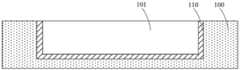
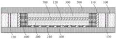
图1为本申请实施例公开的功能封装模块的剖视图;1 is a cross-sectional view of a functional packaging module disclosed in an embodiment of the present application;
图2为本申请实施例公开的功能封装组件的剖视图;2 is a cross-sectional view of a functional package assembly disclosed in an embodiment of the present application;
图3-图11分别为本申请实施例公开的功能封装模块在制备过程中的中间结构示意图。FIG. 3 to FIG. 11 are respectively schematic diagrams of intermediate structures of the functional packaging module disclosed in the embodiments of the present application during the preparation process.
附图标记说明:Description of reference numbers:
100-承载板、101-凹槽、110-第一金属层、120-第二金属层、130-导电结构、140-第二通孔;100-carrying plate, 101-groove, 110-first metal layer, 120-second metal layer, 130-conductive structure, 140-second through hole;
200-第一功能器件、210-金属凸块;200-the first functional device, 210-metal bump;
300-第二功能器件;300-second functional device;
400-第一电连接层;400 - the first electrical connection layer;
500-第二电连接层;500 - the second electrical connection layer;
600-绝缘胶、700-胶膜、800-电连接结构。600-insulating glue, 700-adhesive film, 800-electrical connection structure.
具体实施方式Detailed ways
为使本申请的目的、技术方案和优点更加清楚,下面将结合本申请具体实施例及相应的附图对本申请技术方案进行清楚、完整地描述。显然,所描述的实施例仅是本申请的一部分实施例,而不是全部的实施例。基于本申请中的实施例,本领域普通技术人员在没有做出创造性劳动前提下所获得的所有其他实施例,都属于本申请保护的范围。In order to make the objectives, technical solutions and advantages of the present application clearer, the technical solutions of the present application will be clearly and completely described below with reference to the specific embodiments of the present application and the corresponding drawings. Obviously, the described embodiments are only a part of the embodiments of the present application, but not all of the embodiments. Based on the embodiments in this application, all other embodiments obtained by those of ordinary skill in the art without creative efforts shall fall within the protection scope of this application.
本申请的说明书和权利要求书中的术语“第一”、“第二”等是用于区别类似的对象,而不用于描述特定的顺序或先后次序。应该理解这样使用的数据在适当情况下可以互换,以便本申请的实施例能够以除了在这里图示或描述的那些以外的顺序实施。且“第一”、“第二”等所区分的对象通常为一类,并不限定对象的个数,例如第一对象可以是一个,也可以是多个。此外,说明书以及权利要求中“和/或”表示所连接对象的至少其中之一,字符“/”,一般表示前后关联对象是一种“或”的关系。The terms "first", "second" and the like in the description and claims of the present application are used to distinguish similar objects, and are not used to describe a specific order or sequence. It is to be understood that data so used may be interchanged under appropriate circumstances so that embodiments of the application can be practiced in sequences other than those illustrated or described herein. In addition, the objects distinguished by "first", "second", etc. are usually one type, and the number of objects is not limited. For example, the first object may be one or more than one. In addition, "and/or" in the description and claims indicates at least one of the connected objects, and the character "/" generally indicates that the associated objects are in an "or" relationship.
下面结合附图,通过具体的实施例及其应用场景对本申请各个实施例公开的技术方案进行详细地说明。The technical solutions disclosed in the various embodiments of the present application will be described in detail below through specific embodiments and application scenarios with reference to the accompanying drawings.
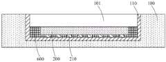
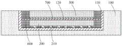
请参考图1,本申请实施例公开一种功能封装模块,所公开的功能封装模块包括承载板100、第一功能器件200、第二功能器件300、第一电连接层400和第二电连接层500。Referring to FIG. 1 , an embodiment of the present application discloses a functional packaging module. The disclosed functional packaging module includes a
承载板100为整个封装模块的基板,承载板100能够起到支撑第一功能器件200、第二功能器件300,第一电连接层400和第二电连接层500的作用。在本申请实施例中,承载板100开设有第一通孔,第一通孔具有第一端口和第二端口。具体的,第一通孔贯穿承载板100的厚度方向。The
第一电连接层400和第二电连接层500为电连接结构800,第一电连接层400设置在第一通孔的第一端口、且第一电连接层400覆盖第一端口,第二电连接层500设置在第一通孔的第二端口、且第二电连接层500覆盖第二端口。The first
第一电连接层400、第二电连接层500和第一通孔的孔壁围成容纳空间,第一功能器件200和第二功能器件300均可以设置在容纳空间之内。第一功能器件200与第一电连接层400电连接,第二功能器件300与第二电连接层500电连接。第一电连接层400和第二电连接层500能够实现位于容纳空间内的第一功能器件200和第二功能器件300与容纳空间之外的电源实施电连接。The first
第一功能器件200和第二功能器件300与容纳空间的内壁之间填充绝缘胶600,进而起到绝缘隔离及固定的作用。The
第一功能器件200和第二功能器件300与容纳空间的内壁之间填充绝缘胶600,绝缘胶600起到将第一功能器件200和第二功能器件300封装在容纳空间之内的作用,从而实现第一功能器件200和第二功能器件300在容纳空间之内的固定,当然,绝缘胶600也起到绝缘隔离的作用。The
本申请实施例公开的功能封装模块中,通过在承载板100开设第一通孔,然后将第一功能器件200和第二功能器件300通过绝缘胶600固定在第一通孔内,并在第一通孔的第一端口和第二端口分别设置第一电连接层400和第二电连接层500,最终使得第一功能器件200和第二功能器件300封装于第一电连接层400、第二电连接层500和第一通孔的孔壁形成的容纳空间中,第一电连接层400和第二电连接层500能够分别实现被封装的第一功能器件200和第二功能器件300的后续接电。通过上述结构可知,本申请实施例公开的功能封装模块能够在承载板100上开设额外的空间,牺牲掉承载板100的部分结构并充分利用这部分结构占用的空间,进而为第一功能器件200和第二功能器件300的提供安装位置。在此种情况下,第一功能器件200和第二功能器件300的设置不会占用承载板100之外的空间,进而能够缓解功能器件的增多而导致的空间问题,有利于减小电子设备的整机尺寸。In the functional package module disclosed in the embodiment of the present application, the first through hole is opened in the
在本申请实施例中,第一通孔的内壁可以设置第一金属层110,第一功能器件200与第二功能器件300之间可以设置第二金属层120。具体的,第二金属层120与第一金属层110连接,从而实现两者之间的电连接。第二金属层120将容纳空间分隔成第一屏蔽空间和第二屏蔽空间,第一功能器件200可以设置于第一屏蔽空间,第二功能器件300可以设置于第二屏蔽空间。第一屏蔽空间能够为第一功能器件200提供电磁屏蔽,进而避免第一功能器件200在工作时被电磁干扰,或者避免第一功能器件200在工作时对其它器件产生电磁干扰。同理,第二屏蔽空间能够为第二功能器件300提供电磁屏蔽,进而避免第二功能器件300在工作时被电磁干扰,或者避免第二功能器件300在工作时对其它器件产生电磁干扰。In this embodiment of the present application, the
与此同时,第一电连接层400和第二电连接层500中的至少一者包括接地层,第一金属层110与接地层电连接。在此种情况下,第一金属层110和第二金属层120产生的静电会通过接地层实现静电泄放,避免对功能封装模块产生静电影响。Meanwhile, at least one of the first
另外,容纳空间被第二金属层120与第一金属层110分隔成第一屏蔽空间和第二屏蔽空间,第一功能器件200和第二功能器件300可以设置于第一屏蔽空间和第二屏蔽空间,从而使得第一功能器件200和第二功能器件300独立运行,并且互相不干扰。In addition, the accommodating space is divided into a first shielding space and a second shielding space by the
如上文所述,第一功能器件200和第二功能器件300均设置在容纳空间之内。具体的,第一功能器件200和第二功能器件300在容纳空间之内具有多种分布方式,本申请实施例不限制第一功能器件200和第二功能器件300的具体分布方式。As described above, both the first
一种可选的实施方式中,第一功能器件200和第二功能器件300可以在承载板100的厚度方向叠置,第一功能器件200邻近第一电连接层400设置、且与第一电连接层400电连接,第二功能器件300邻近第二电连接层500设置、且与第二电连接层500电连接。由于第一电连接层400和第二电连接层500分别设置在第一通孔的两个端口处,而且第一通孔贯穿承载板100的厚度方向,上述布置方式使得第一功能器件200与第一电连接层400的距离较小,进而方便两者之间的电连接。同时,上述布置方式还能够使得第二功能器件300与第二电连接层500之间的距离较小,进而方便两者之间的电连接。In an optional implementation manner, the first
如上文所述,第一功能器件200和第二功能器件300在承载板100的厚度方向叠置,具体的,第二功能器件300支撑于第一功能器件200上,如上文所述,第二金属层120可以设置在第一功能器件200与第二功能器件300之间,为了避免第二金属层120对第二功能器件300产生影响,第二金属层120与第二功能器件300之间可以设置有胶膜700,从而实现更好地隔离。当然,第二金属层120与第二功能器件300之间也可以通过绝缘胶600隔离。As described above, the first
在本申请实施例中,第一功能器件200和第二功能器件300的种类可以有多种,例如,第一功能器件200和第二功能器件300可以为电阻器件、电容器件、电感器件,当然,也可以为芯片,本申请实施例对第一功能器件200和第二功能器件300的具体类别不做限制。In this embodiment of the present application, the first
在一种可行的方案中,第一功能器件200可以为第一芯片,第二功能器件300可以为第二芯片。具体的,第一芯片的功能面朝向第一电连接层400,进而使得第一芯片的功能部分更方便接电。同理,第二芯片的功能面朝向第二电连接层500,进而使得第二芯片的功能部分更方便接电。In a feasible solution, the first
与此同时,第一芯片的功能面的朝向与第二芯片的功能面的朝向相背,从而能够使得两者的功能面处于相对距离较大的位置,避免产生可能存在的相互干扰。需要说明的是,本文中,功能面,指的是芯片设置器件的一侧的表面。At the same time, the orientation of the functional surface of the first chip is opposite to the orientation of the functional surface of the second chip, so that the functional surfaces of the two are located at relatively large distances to avoid possible mutual interference. It should be noted that, in this document, the functional surface refers to the surface on the side of the chip on which the device is disposed.
在本申请实施例中,第一功能器件200与第一电连接层400的电连接方式和第二功能器件300与第二电连接层500的电连接方式可以有多种。例如通过在绝缘胶600内埋设电连接结构件(例如电连接线),通过电连接结构件实现电连接。In the embodiment of the present application, there may be various ways of electrical connection between the first
在第一功能器件200为第一芯片,第二功能器件300为第二芯片的情况下,第一芯片和第二芯片中的至少一者可以设置有金属凸块210,金属凸块210可以与第一电连接层400或第二电连接层500电连接。具体的,第一芯片可以设置有金属凸块210,金属凸块210可以与第一电连接层400电连接。当然,第二芯片也可以设置金属凸块210,第二芯片通过其上设置的金属凸块210实现与第二电连接层500的电连接。In the case where the first
在通常情况下,金属凸块210为设置在第一芯片或第二芯片上的金属焊盘,此种情况下,可以充分利用第一芯片或第二芯片已有的结构实现电连接,无疑更容易实现。与此同时,金属凸块210还能够起到较好地支撑的作用,使得第一芯片或第二芯片在容纳空间内的位置更加稳定。Under normal circumstances, the metal bumps 210 are metal pads disposed on the first chip or the second chip. In this case, the existing structure of the first chip or the second chip can be fully utilized to achieve electrical connection. easy to accomplish. At the same time, the metal bumps 210 can also play a better supporting role, so that the position of the first chip or the second chip in the accommodating space is more stable.
在进一步的技术方案中,金属凸块210的数量为多个,多个金属凸块210阵列分布在第一芯片或第二芯片上,多个金属凸块210均与第一电连接层400或第二电连接层500电连接,此种多点电连接的连接方式,能够更好地避免可能被绝缘胶600覆盖而导致的电连接失效,进而有利于提高第一芯片与第一电连接层400或第二芯片与第二电连接层500之间电连接的可靠性。In a further technical solution, the number of
在具体的安装过程中,功能封装模块通常安装于电子设备内的电路板(例如主板)上,进而与电路板电连接,进而由电路板供电或控制。具体的,第一电连接层400可以通过单独的电连接结构800(例如电线)实现与电路板的电连接,第二电连接层500可以通过单独的电连接结构800(例如电线)实现与电路板的电连接。In a specific installation process, the functional package module is usually installed on a circuit board (eg, a mainboard) in an electronic device, and then electrically connected to the circuit board, and then powered or controlled by the circuit board. Specifically, the first
为了使得第一功能器件200和第二功能器件300更方便接电,一种可选的方案中,承载板100可以开设有第二通孔140,第二通孔140内可以设置导电结构130,第一电连接层400和第二电连接层500通过导电结构130电连接,以功能封装模块的第二电连接层500安装在承载板100为例,第一功能器件200可以依次通过第一电连接层400、导电结构130和第二电连接层500实现与电路板的电连接,第二功能器件300通过第二电连接层500实现与电路板之间的电连接。需要说明的是,第一功能器件200和第二功能器件300共用第二电连接层500电连接的过程中,若有必要,第二电连接层500可以设置相互独立的电连接结构800,避免相互之间电连接的影响。In order to make the power connection of the first
上述电连接结构800中,在功能封装模块向电路板安装的过程中,只需要将第一电连接层400或第二电连接层500与电路板电连接即可,第二通孔140内设置的导电结构130实现第一电连接层400和第二电连接层500电连接的同时,由于导电结构130设置在第二通孔140内,因此同样不会占用额外的空间,有利于功能封装模块的小型化。In the above
与此同时,承载板100能够对导电结构130实施防护,避免环境中其它器件安装过程中对导电结构130的电连接稳定性产生影响。At the same time, the
如上文所述,第二通孔140内可以设置导电结构130,导电结构130的制造材料可以为导电金属材料,导电结构130可以是金属线、导电涂层。一种可行的方案中,导电结构130可以为设置在第二通孔140的内壁上的第三金属层,第三金属层可以为金属镀层、金属涂层等。As described above, the
在本申请实施例中,第一电连接层400或第二电连接层500可以设置有电连接结构800,在一种可行的方案中,电连接结构800为功能封装模块的接电部,进而方便功能封装模块与电路板之间的电连接。具体的,电连接结构800可以为阵列分布于第一电连接层400或第二电连接层500的焊接球。In the embodiment of the present application, the first
在本申请实施例中,承载板100是第一功能器件200和第二功能器件300的安装基础,同时,承载板100也起到防护作用,承载板100可选择强度较好的材料制成。例如,承载板100可以为陶瓷基板。一种可选的方案中,承载板100可以为硅基板,硅基板具有较好的机械加工性能,在现有工艺的条件下,硅基板能够被切割成更薄的结构件,有利于进一步减小整个功能封装模块的厚度。In the embodiment of the present application, the
基于本申请实施例公开的功能封装模块,本申请实施例公开一种功能封装组件,请参考图2,所公开的功能封装组件包括至少两个功能封装模块。任意相邻的两个功能封装模块的承载板100叠置,且相邻的两个功能封装模块电连接。在此种情况下,功能封装组件可通过邻近电子设备的电路板(例如电子设备的主板)的功能封装模块实现与电路板之间的电连接。Based on the functional encapsulation module disclosed in the embodiment of the present application, the embodiment of the present application discloses a functional encapsulation component. Please refer to FIG. 2 . The disclosed functional encapsulation component includes at least two functional encapsulation modules. The
具体的,在第一电连接层400或第二电连接层500设置有电连接结构800的情况下,与电路板邻近的功能封装模块可以通过电连接结构800与电路板电连接。Specifically, when the first
当然,相邻的两个功能封装模块可以通过焊接、粘接、螺纹连接件实现叠置状态下的连接。一种可行的方式中,两个功能封装模块可以通过焊接的方式叠置,具体的,在一个功能封装模块的第一电连接层400或第二电连接层500可以设置有焊盘,焊接球可以设置于焊盘,两个功能封装模块可以通过焊接球焊接叠置,且相邻的两个功能封装模块电连接。Of course, two adjacent functional packaging modules can be connected in a stacked state by welding, gluing, or screwing. In a feasible way, two functional packaging modules can be stacked by welding. Specifically, the first
基于本申请实施例公开的功能封装组件,本申请实施例公开一种电子设备,所公开的电子设备包括上文实施例所述的功能封装组件。Based on the functional packaging components disclosed in the embodiments of the present application, the embodiments of the present application disclose an electronic device, and the disclosed electronic device includes the functional packaging components described in the above embodiments.
本申请实施例公开的电子设备可以为手机、电脑、电子书阅读器、游戏机、可穿戴设备等,当然,电子设备还可以为其它种类的设备,本申请实施例不限制电子设备的具体种类。The electronic devices disclosed in the embodiments of the present application may be mobile phones, computers, e-book readers, game consoles, wearable devices, etc. Of course, the electronic devices may also be other types of devices, and the embodiments of the present application do not limit the specific types of electronic devices .
请参考图3至图11,本申请实施例公开一种功能封装模块的制作方法,所公开的制作方法包括:Please refer to FIG. 3 to FIG. 11 , an embodiment of the present application discloses a method for manufacturing a functional package module. The disclosed manufacturing method includes:
步骤011、在承载板100开设凹槽101。Step 011 , opening a
本步骤可以通过机械加工、蚀刻等方式实现在承载板100上加工凹槽101,具体的,凹槽101的深度方向与承载板100的厚度方向一致。In this step, the
步骤012、将第一功能器件200和第二功能器件300设置于凹槽101内以及向凹槽101内填充绝缘胶600。Step 012 , disposing the first
本步骤中,绝缘胶600填充于第一功能器件200和第二功能器件300与凹槽101的内壁之间,且第一功能器件200和第二功能器件300相互隔离,同时绝缘胶600至少起到将第一功能器件200和第二功能器件300固定在承载板100上的作用。当然,第一功能器件200与第二功能器件300之间可以通过部分绝缘胶600实现相互隔离。In this step, the insulating
步骤013、去除承载板100上与凹槽101的底壁所在的一侧的部分材料,以使凹槽101形成第一通孔。Step 013 , removing part of the material on the
步骤014、在第一通孔的第一端口设置第一电连接层400以及在第一通孔的第二端口设置第二电连接层500,以使第一电连接层400与第一功能器件200电连接以及第二电连接层500与第二功能器件300电连接。Step 014: Disposing the first
在本实施例中,第一电连接层400和第二电连接层500均可以为RDL层。当然,还可以为其他种类的电连接层,例如金属镀层、金属涂层等,本申请实施例不限制第一电连接层400和第二电连接层500的具体种类。In this embodiment, both the first
在进一步的技术方案中,步骤012可以包括:In a further technical solution, step 012 may include:
步骤021、将第一功能器件200支撑于凹槽101的底壁,第一功能器件200朝向底壁的一侧设置有金属凸块210,金属凸块210支撑于底壁;Step 021 , supporting the first
步骤022、向凹槽101内填充绝缘胶600,以使绝缘胶600填充于第一功能器件200与凹槽101的内壁之间,且绝缘胶600朝向凹槽101的槽口的第一表面与第一功能器件200朝向所述槽口的第二表面平齐;Step 022 , filling the
步骤023、在第二表面上设置绝缘隔离层。具体的,绝缘隔离层可以为胶膜700。Step 023, disposing an insulating isolation layer on the second surface. Specifically, the insulating isolation layer may be the
步骤024、在隔离层上设置第二功能器件300;Step 024, setting the second
步骤025、向第二功能器件300与凹槽101的内壁之间的空间内再次填充绝缘胶600。Step 025 , filling the space between the second
在更进一步的技术方案中,在承载板100开设凹槽101之后,还可以包括:在凹槽101的内壁设置第一金属层110。在第二表面上设置绝缘隔离层之前,还可以包括:在第一表面与第二表面形成的支撑面上设置第二金属层120,并连接第一金属层110和第二金属层120,以使第一金属层110与第二金属层120围成相互隔离的第一屏蔽空间和第二屏蔽空间,绝缘隔离层设置于第二金属层120上。此种方案中能够形成相互隔离的第一屏蔽空间和第二屏蔽空间,从而能够对第一功能器件200和第二功能器件300起到隔离屏蔽的作用,避免被电磁干扰或对其他器件产生电磁干扰。In a further technical solution, after the
当然,步骤014在实施的过程中,在第一端口设置第一电连接层400与在第二端口设置第二电连接层500之间还可以包括:在承载板100上开设第二通孔140,并在第二通孔140内设置导电结构130,以使导电结构130能够电连接第一电连接层400与第二电连接层500。Of course, during the implementation of step 014, between the setting of the first
本申请上文实施例中重点描述的是各个实施例之间的不同,各个实施例之间不同的优化特征只要不矛盾,均可以组合形成更优的实施例,考虑到行文简洁,在此则不再赘述。The above embodiments of this application mainly describe the differences between the various embodiments. As long as the different optimization features of the various embodiments are not contradictory, they can be combined to form better embodiments. No longer.
以上所述仅为本申请的实施例而已,并不用于限制本申请。对于本领域技术人员来说,本申请可以有各种更改和变化。凡在本申请的精神和原理之内所作的任何修改、等同替换、改进等,均应包含在本申请的权利要求范围之内。The above descriptions are merely examples of the present application, and are not intended to limit the present application. Various modifications and variations of this application are possible for those skilled in the art. Any modification, equivalent replacement, improvement, etc. made within the spirit and principle of the present application shall be included within the scope of the claims of the present application.
Claims (14)
Priority Applications (1)
| Application Number | Priority Date | Filing Date | Title |
|---|---|---|---|
| CN202011014037.1ACN112151458B (en) | 2020-09-24 | 2020-09-24 | Functional packaging module and preparation method thereof, functional packaging assembly and electronic equipment |
Applications Claiming Priority (1)
| Application Number | Priority Date | Filing Date | Title |
|---|---|---|---|
| CN202011014037.1ACN112151458B (en) | 2020-09-24 | 2020-09-24 | Functional packaging module and preparation method thereof, functional packaging assembly and electronic equipment |
Publications (2)
| Publication Number | Publication Date |
|---|---|
| CN112151458Atrue CN112151458A (en) | 2020-12-29 |
| CN112151458B CN112151458B (en) | 2022-11-25 |
Family
ID=73896492
Family Applications (1)
| Application Number | Title | Priority Date | Filing Date |
|---|---|---|---|
| CN202011014037.1AActiveCN112151458B (en) | 2020-09-24 | 2020-09-24 | Functional packaging module and preparation method thereof, functional packaging assembly and electronic equipment |
Country Status (1)
| Country | Link |
|---|---|
| CN (1) | CN112151458B (en) |
Citations (7)
| Publication number | Priority date | Publication date | Assignee | Title |
|---|---|---|---|---|
| CN101276805A (en)* | 2007-06-15 | 2008-10-01 | 日月光半导体制造股份有限公司 | Semiconductor package structure with electromagnetic interference shielding function and manufacturing method thereof |
| US20090127686A1 (en)* | 2007-11-21 | 2009-05-21 | Advanced Chip Engineering Technology Inc. | Stacking die package structure for semiconductor devices and method of the same |
| US20100244208A1 (en)* | 2009-03-25 | 2010-09-30 | Stats Chippac, Ltd. | Semiconductor Device and Method of Forming a Shielding Layer Between Stacked Semiconductor Die |
| CN102364683A (en)* | 2011-10-21 | 2012-02-29 | 华为终端有限公司 | Packaging structure and method thereof, and electronic equipment |
| CN107452720A (en)* | 2017-08-03 | 2017-12-08 | 华天科技(昆山)电子有限公司 | Chip fan-out packaging structure, multi-chip integrated module and wafer-level packaging method |
| CN209029359U (en)* | 2018-11-23 | 2019-06-25 | 华进半导体封装先导技术研发中心有限公司 | A kind of chip chamber full-shield encapsulating structure based on substrate embedment technical module |
| CN110364490A (en)* | 2018-04-11 | 2019-10-22 | 中国科学院微电子研究所 | A chip packaging structure and packaging method thereof |
- 2020
- 2020-09-24CNCN202011014037.1Apatent/CN112151458B/enactiveActive
Patent Citations (7)
| Publication number | Priority date | Publication date | Assignee | Title |
|---|---|---|---|---|
| CN101276805A (en)* | 2007-06-15 | 2008-10-01 | 日月光半导体制造股份有限公司 | Semiconductor package structure with electromagnetic interference shielding function and manufacturing method thereof |
| US20090127686A1 (en)* | 2007-11-21 | 2009-05-21 | Advanced Chip Engineering Technology Inc. | Stacking die package structure for semiconductor devices and method of the same |
| US20100244208A1 (en)* | 2009-03-25 | 2010-09-30 | Stats Chippac, Ltd. | Semiconductor Device and Method of Forming a Shielding Layer Between Stacked Semiconductor Die |
| CN102364683A (en)* | 2011-10-21 | 2012-02-29 | 华为终端有限公司 | Packaging structure and method thereof, and electronic equipment |
| CN107452720A (en)* | 2017-08-03 | 2017-12-08 | 华天科技(昆山)电子有限公司 | Chip fan-out packaging structure, multi-chip integrated module and wafer-level packaging method |
| CN110364490A (en)* | 2018-04-11 | 2019-10-22 | 中国科学院微电子研究所 | A chip packaging structure and packaging method thereof |
| CN209029359U (en)* | 2018-11-23 | 2019-06-25 | 华进半导体封装先导技术研发中心有限公司 | A kind of chip chamber full-shield encapsulating structure based on substrate embedment technical module |
Also Published As
| Publication number | Publication date |
|---|---|
| CN112151458B (en) | 2022-11-25 |
Similar Documents
| Publication | Publication Date | Title |
|---|---|---|
| CN105074918B (en) | Stacked memory package, method of manufacturing same and pinout design of IC package substrate | |
| CN103688353B (en) | Microelectronic device, stacked die package, and computing system including stacked die package, method of fabricating a multi-channel communication path in a stacked die package, and method of enabling electrical communication between components of a stacked die package | |
| TW462125B (en) | Semiconductor device and manufacturing method therefor | |
| JP6097837B2 (en) | System in package with RF die embedded in coreless substrate | |
| US20190051615A1 (en) | Systems, methods, and apparatuses for implementing an organic stiffener with an emi shield for rf integration | |
| KR20140057982A (en) | Semiconductor package and method of manufacturing the semiconductor package | |
| KR20140057979A (en) | Semiconductor package and method of manufacturing the semiconductor package | |
| EP4030475A1 (en) | Encapsulation structure and electronic apparatus | |
| JP2012109572A (en) | Semiconductor package, semiconductor module, electronic device, and manufacturing method for semiconductor package | |
| KR20120060665A (en) | Semiconductor package | |
| KR101935502B1 (en) | Semiconductor chip and semiconductor package having the same | |
| CN212209463U (en) | Package structure and electronic device | |
| US8084856B2 (en) | Thermal spacer for stacked die package thermal management | |
| KR102160786B1 (en) | Semiconductor Packages | |
| EP2555239A2 (en) | Thermal package with heat slug for die stacks | |
| CN110808240A (en) | Package-on-package structure and method for manufacturing the same | |
| KR20090083709A (en) | Printed circuit board, semiconductor package, card and system | |
| CN107482002A (en) | Semiconductor component with package-on-package structure and electronic equipment including the same | |
| TW201347120A (en) | Semiconductor chip, semiconductor package having the same, and stacked semiconductor package using the semiconductor package | |
| US7332801B2 (en) | Electronic device | |
| CN101031995B (en) | Split Film Capacitors for Multi-Voltage | |
| CN103855128B (en) | Semiconductor device | |
| CN112151458B (en) | Functional packaging module and preparation method thereof, functional packaging assembly and electronic equipment | |
| TWI226693B (en) | BAG package and printed circuit board for supporting the package | |
| CN211150559U (en) | Multi-chip packaging module |
Legal Events
| Date | Code | Title | Description |
|---|---|---|---|
| PB01 | Publication | ||
| PB01 | Publication | ||
| SE01 | Entry into force of request for substantive examination | ||
| SE01 | Entry into force of request for substantive examination | ||
| GR01 | Patent grant | ||
| GR01 | Patent grant |