CN112151386B - Stacked nanowire ring gate device and manufacturing method thereof - Google Patents
Stacked nanowire ring gate device and manufacturing method thereofDownload PDFInfo
- Publication number
- CN112151386B CN112151386BCN202011036930.4ACN202011036930ACN112151386BCN 112151386 BCN112151386 BCN 112151386BCN 202011036930 ACN202011036930 ACN 202011036930ACN 112151386 BCN112151386 BCN 112151386B
- Authority
- CN
- China
- Prior art keywords
- layer
- side wall
- etching
- stacked
- sidewall
- Prior art date
- Legal status (The legal status is an assumption and is not a legal conclusion. Google has not performed a legal analysis and makes no representation as to the accuracy of the status listed.)
- Active
Links
Images


Classifications
- H—ELECTRICITY
- H10—SEMICONDUCTOR DEVICES; ELECTRIC SOLID-STATE DEVICES NOT OTHERWISE PROVIDED FOR
- H10D—INORGANIC ELECTRIC SEMICONDUCTOR DEVICES
- H10D64/00—Electrodes of devices having potential barriers
- H10D64/01—Manufacture or treatment
- H10D64/017—Manufacture or treatment using dummy gates in processes wherein at least parts of the final gates are self-aligned to the dummy gates, i.e. replacement gate processes
- H—ELECTRICITY
- H10—SEMICONDUCTOR DEVICES; ELECTRIC SOLID-STATE DEVICES NOT OTHERWISE PROVIDED FOR
- H10D—INORGANIC ELECTRIC SEMICONDUCTOR DEVICES
- H10D30/00—Field-effect transistors [FET]
- H10D30/60—Insulated-gate field-effect transistors [IGFET]
- H10D30/62—Fin field-effect transistors [FinFET]
- H—ELECTRICITY
- H10—SEMICONDUCTOR DEVICES; ELECTRIC SOLID-STATE DEVICES NOT OTHERWISE PROVIDED FOR
- H10D—INORGANIC ELECTRIC SEMICONDUCTOR DEVICES
- H10D62/00—Semiconductor bodies, or regions thereof, of devices having potential barriers
- H10D62/10—Shapes, relative sizes or dispositions of the regions of the semiconductor bodies; Shapes of the semiconductor bodies
- H10D62/117—Shapes of semiconductor bodies
- H10D62/118—Nanostructure semiconductor bodies
- H10D62/119—Nanowire, nanosheet or nanotube semiconductor bodies
- H10D62/121—Nanowire, nanosheet or nanotube semiconductor bodies oriented parallel to substrates
- H—ELECTRICITY
- H10—SEMICONDUCTOR DEVICES; ELECTRIC SOLID-STATE DEVICES NOT OTHERWISE PROVIDED FOR
- H10D—INORGANIC ELECTRIC SEMICONDUCTOR DEVICES
- H10D62/00—Semiconductor bodies, or regions thereof, of devices having potential barriers
- H10D62/10—Shapes, relative sizes or dispositions of the regions of the semiconductor bodies; Shapes of the semiconductor bodies
- H10D62/124—Shapes, relative sizes or dispositions of the regions of semiconductor bodies or of junctions between the regions
- H—ELECTRICITY
- H10—SEMICONDUCTOR DEVICES; ELECTRIC SOLID-STATE DEVICES NOT OTHERWISE PROVIDED FOR
- H10D—INORGANIC ELECTRIC SEMICONDUCTOR DEVICES
- H10D64/00—Electrodes of devices having potential barriers
- H10D64/01—Manufacture or treatment
- H10D64/021—Manufacture or treatment using multiple gate spacer layers, e.g. bilayered sidewall spacers
- H—ELECTRICITY
- H10—SEMICONDUCTOR DEVICES; ELECTRIC SOLID-STATE DEVICES NOT OTHERWISE PROVIDED FOR
- H10D—INORGANIC ELECTRIC SEMICONDUCTOR DEVICES
- H10D64/00—Electrodes of devices having potential barriers
- H10D64/20—Electrodes characterised by their shapes, relative sizes or dispositions
- H10D64/27—Electrodes not carrying the current to be rectified, amplified, oscillated or switched, e.g. gates
- H10D64/311—Gate electrodes for field-effect devices
- H10D64/411—Gate electrodes for field-effect devices for FETs
- H10D64/511—Gate electrodes for field-effect devices for FETs for IGFETs
- H10D64/512—Disposition of the gate electrodes, e.g. buried gates
Landscapes
- Thin Film Transistor (AREA)
Abstract
Description
Translated fromChinese技术领域technical field
本发明设计半导体制备技术领域,尤其涉及一种堆叠纳米线环栅器件及其制作方法。The invention relates to the technical field of semiconductor preparation, in particular to a stacked nanowire gate-around device and a manufacturing method thereof.
背景技术Background technique
5纳米以下集成电路技术中现有的FinFET器件结构面临诸多挑战。环栅纳米线器件由于具有更好的沟道静电完整性、漏电流控制和载流子一维弹道输运等优势,被认为是延续摩尔定律的关键架构之一。近年来,将理想环栅纳米线结构和主流FinFET工艺结合发展下一代集成技术已成为集成电路深入发展的研发关键热点之一。Existing FinFET device structures in integrated circuit technologies below 5nm face many challenges. Due to the advantages of better channel electrostatic integrity, leakage current control and one-dimensional ballistic transport of carriers, the gate-all-around nanowire device is considered to be one of the key architectures to continue Moore's Law. In recent years, the combination of ideal gate-all-around nanowire structure and mainstream FinFET technology to develop next-generation integration technology has become one of the key R&D hotspots for the in-depth development of integrated circuits.
堆叠纳米线/片的释放是实现环栅器件集成技术的关键点。一般采用内侧墙(inner spacer)技术防止纳米线释放时的横向腐蚀,以免影响器件实际栅长,甚至造成器件短路造成失效。淀积内侧墙的材料一般是Si3N4,淀积完成后需要将顶部和侧壁的Si3N4材料全部刻蚀干净,仅保留极少一部分存在于内侧墙的Si3N4,这就给干法刻蚀工艺带来了极大的难度,当干法刻蚀工艺偏向于各向异性时无法刻蚀完全侧壁的Si3N4,而当干法刻蚀工艺偏向于各向同性时又极容易将内侧墙的Si3N4也刻蚀殆尽,这个平衡点极难控制。The release of stacked nanowires/sheets is a key point to realize gate-all-around device integration technology. Generally, the inner spacer technology is used to prevent the lateral corrosion when the nanowires are released, so as not to affect the actual gate length of the device, or even cause the device to short circuit and cause failure. The material for depositing the inner wall is generally Si3 N4 . After the deposition is completed, all the Si3 N4 materials on the top and side walls need to be etched away, leaving only a small part of Si3 N4 existing in the inner wall. It brings great difficulty to the dry etching process. When the dry etching process is biased towards anisotropy, Si3 N4 with complete sidewalls cannot be etched, while when the dry etching process is biased towards anisotropy It is very easy to etch away the Si3 N4 on the inner wall when it is the same sex, and this balance point is extremely difficult to control.
发明内容Contents of the invention
有鉴于此,本发明的主要目的在于提出一种堆叠纳米线环栅器件及其制作方法,以期至少部分地解决上述提及的技术问题中的至少之一。In view of this, the main purpose of the present invention is to provide a stacked nanowire gate-all-around device and its manufacturing method, in order to at least partially solve at least one of the above-mentioned technical problems.
为实现上述目的,本发明的技术方案包括:To achieve the above object, technical solutions of the present invention include:
作为本发明的一个方面,提供一种堆叠纳米线环栅器件的制作方法,包括如下步骤:As an aspect of the present invention, a method for fabricating a stacked nanowire gate-all-around device is provided, comprising the following steps:
在衬底上通过外延方式依次交替生长牺牲层和沟道层,形成堆叠结构;Alternately growing sacrificial layers and channel layers on the substrate by means of epitaxy to form a stacked structure;
在所述堆叠结构上制作假栅;making dummy gates on the stacked structure;
在所述假栅上制作第一侧墙层;making a first side wall layer on the dummy gate;
从各所述牺牲层的裸露表面开始向内刻蚀,在所述堆叠结构上形成相对所述沟道层的内凹形貌;Etching inwards from the exposed surface of each sacrificial layer to form a concave topography opposite to the channel layer on the stacked structure;
淀积第二侧墙层,并填充所述内凹形貌的内凹处形成内侧墙;depositing a second sidewall layer, and filling the concave part of the concave shape to form an inner wall;
在所述第二侧墙层上淀积填充层,平坦化至使第二侧墙层裸露;depositing a filling layer on the second sidewall layer, and planarizing to expose the second sidewall layer;
通过自对准刻蚀方式刻蚀第二侧墙层的顶部和侧壁,剩余内侧墙以及被填充层覆盖的第二侧墙层的底部;Etching the top and sidewalls of the second sidewall layer, the remaining inner sidewall and the bottom of the second sidewall layer covered by the filling layer by self-aligned etching;
去除所述填充层和第二侧墙层的底部;removing the fill layer and the bottom of the second sidewall layer;
在所述衬底上分别外延生长源区和漏区;respectively epitaxially growing a source region and a drain region on the substrate;
湿法腐蚀去除所述假栅和第一侧墙层;removing the dummy gate and the first spacer layer by wet etching;
去除所述牺牲层,形成纳米线沟道;removing the sacrificial layer to form a nanowire channel;
形成环绕所述纳米线沟道的高K金属栅;forming a high-k metal gate surrounding the nanowire channel;
填充绝缘层,制作接触孔和引线,完成制备。Fill the insulating layer, make contact holes and leads, and complete the preparation.
作为本发明的另一个方面,还提供一种堆叠纳米线环栅器件,采用如上所述的堆叠纳米线环栅器件的制作方法制备得到。As another aspect of the present invention, there is also provided a stacked nanowire gate-around device, which is prepared by adopting the manufacturing method of the above-mentioned stacked nanowire gate-around device.
基于上述技术方案,本发明相较于现有技术,至少具有以下有益效果的其中之一或其中一部分:Based on the above technical solution, compared with the prior art, the present invention has at least one or part of the following beneficial effects:
本发明提出了一种工艺简单,与集成电路工艺相兼容且适宜批量生产的方式进行干法刻蚀形成内侧墙,在保留内侧墙的同时刻蚀完全侧壁的侧墙层;在侧墙层淀积后,通过填充层填充并回刻,进一步自对准方式刻蚀侧壁层,从而得到完整的内侧墙,最终得到栅长保持一致的堆叠纳米线环栅器件;The invention proposes a method with simple process, compatible with integrated circuit technology and suitable for mass production to form the inner wall by dry etching, and to etch the side wall layer of the complete side wall while retaining the inner wall; in the side wall layer After deposition, the filling layer is filled and etched back, and the sidewall layer is further etched in a self-aligned manner to obtain a complete inner wall, and finally a stacked nanowire gate-around device with consistent gate length is obtained;
本发明通过自对准方式刻蚀第二侧墙层的顶部和侧壁;通过各向异性刻蚀方式去除第二侧墙层底部;工艺简单且适宜批量生产;The invention etches the top and sidewall of the second sidewall layer by self-alignment; removes the bottom of the second sidewall layer by anisotropic etching; the process is simple and suitable for mass production;
本发明通过旋涂碳或者聚酰亚胺作为填充层,在刻蚀侧墙层时选择比较高,且容易通过灰化工艺去除。The present invention uses spin-coated carbon or polyimide as the filling layer, which has relatively high selection when etching the sidewall layer and is easy to remove through the ashing process.
附图说明Description of drawings
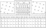
图1为本发明实施例的堆叠纳米线环栅器件示意图;1 is a schematic diagram of a stacked nanowire gate-all-around device according to an embodiment of the present invention;
图2为本发明实施例的在衬底上形成堆叠层的示意图;2 is a schematic diagram of forming stacked layers on a substrate according to an embodiment of the present invention;
图3为本发明实施例的在图2的结构上形成堆叠结构的示意图;FIG. 3 is a schematic diagram of forming a stacked structure on the structure in FIG. 2 according to an embodiment of the present invention;
图4为本发明实施例的在图3的结构上形成假栅和第一侧墙层的示意图;FIG. 4 is a schematic diagram of forming a dummy gate and a first spacer layer on the structure in FIG. 3 according to an embodiment of the present invention;
图5为本发明实施例的在图4的结构上形成内凹形貌的示意图;Fig. 5 is a schematic diagram of forming a concave shape on the structure of Fig. 4 according to an embodiment of the present invention;
图6为本发明实施例的在图5的结构上形成第二侧墙层的示意图;6 is a schematic diagram of forming a second sidewall layer on the structure of FIG. 5 according to an embodiment of the present invention;
图7为本发明实施例的在图6的结构上形成填充层的示意图;FIG. 7 is a schematic diagram of forming a filling layer on the structure of FIG. 6 according to an embodiment of the present invention;
图8为本发明实施例的在图7的结构上将填充层平坦化的示意图;FIG. 8 is a schematic diagram of planarizing a filling layer on the structure of FIG. 7 according to an embodiment of the present invention;
图9为本发明实施例的在图8的结构上刻蚀第二侧墙层的顶部和侧壁的示意图;FIG. 9 is a schematic diagram of etching the top and sidewalls of the second sidewall layer on the structure of FIG. 8 according to an embodiment of the present invention;
图10为本发明实施例的在图9的结构上去除填充层和第二侧墙层的底部的示意图;FIG. 10 is a schematic diagram of removing the filling layer and the bottom of the second side wall layer on the structure of FIG. 9 according to an embodiment of the present invention;
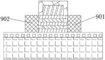
图11为本发明实施例的在图10的结构上生长源区和漏区的示意图。FIG. 11 is a schematic diagram of growing a source region and a drain region on the structure of FIG. 10 according to an embodiment of the present invention.
以上附图中,附图标记含义如下:In the above accompanying drawings, the reference signs have the following meanings:
1、SOI片;2、堆叠层;201、Si层;202、SiGe层;3、堆叠结构;4、假栅;5、第一侧墙层;6、第二侧墙层;7、填充层;8、内侧墙;901、源区;902、漏区;10、绝缘层、11、引线;12、高K金属栅。1. SOI sheet; 2. Stacked layer; 201, Si layer; 202, SiGe layer; 3. Stacked structure; 4. Dummy gate; 5. First sidewall layer; 6. Second sidewall layer; 7. Filling layer ; 8, inner wall; 901, source region; 902, drain region; 10, insulating layer, 11, lead; 12, high-K metal gate.
具体实施方式detailed description
为使本发明的目的、技术方案和优点更加清楚明白,以下结合具体实施例,并参照附图,对本发明作进一步的详细说明。In order to make the object, technical solution and advantages of the present invention clearer, the present invention will be further described in detail below in conjunction with specific embodiments and with reference to the accompanying drawings.
作为本发明的一个方面,提供一种堆叠纳米线环栅器件的制作方法,包括如下步骤:As an aspect of the present invention, a method for fabricating a stacked nanowire gate-all-around device is provided, comprising the following steps:
在衬底上通过外延方式依次交替生长牺牲层和沟道层,形成堆叠结构;Alternately growing sacrificial layers and channel layers on the substrate by means of epitaxy to form a stacked structure;
在堆叠结构上制作假栅;Make dummy gates on stacked structures;
在假栅上制作第一侧墙层;Make the first side wall layer on the dummy grid;
从各牺牲层的裸露表面开始向内刻蚀,在堆叠结构上形成相对沟道层的内凹形貌;Starting from the exposed surface of each sacrificial layer to etch inward, forming a concave shape opposite to the channel layer on the stacked structure;
淀积第二侧墙层,并填充内凹形貌的内凹处形成内侧墙;depositing a second side wall layer, and filling the concave part of the concave shape to form an inner wall;
在第二侧墙层上淀积填充层,平坦化至使第二侧墙层裸露;depositing a filling layer on the second side wall layer, and planarizing to expose the second side wall layer;
通过自对准刻蚀方式刻蚀第二侧墙层的顶部和侧壁,剩余内侧墙以及被填充层覆盖的第二侧墙层的底部;Etching the top and sidewalls of the second sidewall layer, the remaining inner sidewall and the bottom of the second sidewall layer covered by the filling layer by self-aligned etching;
去除填充层和第二侧墙层的底部;Removal of the fill layer and the bottom of the second sidewall layer;
在衬底上分别外延生长源区和漏区;Epitaxially growing source and drain regions on the substrate;
湿法腐蚀去除假栅和第一侧墙层;Wet etching removes the dummy gate and the first sidewall layer;
去除牺牲层,形成纳米线沟道;removing the sacrificial layer to form a nanowire channel;
形成环绕纳米线沟道的高K金属栅;forming a high-k metal gate surrounding the nanowire channel;
填充绝缘层,制作接触孔和引线,完成制备。Fill the insulating layer, make contact holes and leads, and complete the preparation.
在本发明的实施例中,形成堆叠结构步骤中,具体包括如下子步骤:In an embodiment of the present invention, the step of forming a stacked structure specifically includes the following sub-steps:
在衬底上通过外延方式依次交替生长牺牲层和沟道层,形成堆叠层;Alternately growing sacrificial layers and channel layers on the substrate by means of epitaxy to form stacked layers;
利用光刻技术,在堆叠层上形成图案化的光刻胶;Form a patterned photoresist on the stack layer by using photolithography technology;
以图案化的光刻胶为掩膜,干法刻蚀堆叠层至衬底;Using the patterned photoresist as a mask, dry etching the stacked layers to the substrate;
去除光刻胶,形成堆叠结构。The photoresist is removed to form a stacked structure.
在本发明的实施例中,形成内凹形貌的步骤中,采用原子层刻蚀方式刻蚀各牺牲层;In an embodiment of the present invention, in the step of forming the concave shape, each sacrificial layer is etched by atomic layer etching;
其中,内凹形貌的相对沟道层的内凹深度与第一侧墙层的厚度相同。Wherein, the concave depth of the concave shape relative to the channel layer is the same as the thickness of the first sidewall layer.
在本发明的实施例中,淀积第二侧墙层步骤中,第二侧墙层的材料包括氮化硅、一氮化硅、碳化硅或者氮氧化硅。In an embodiment of the present invention, in the step of depositing the second sidewall layer, the material of the second sidewall layer includes silicon nitride, silicon nitride, silicon carbide or silicon oxynitride.
在本发明的实施例中,淀积填充层并平坦化的步骤中,填充层的材料包括旋涂碳或者聚酰亚胺;In an embodiment of the present invention, in the step of depositing the filling layer and planarizing, the material of the filling layer includes spin-on carbon or polyimide;
平坦化的方式包括干法刻蚀或者化学机械抛光。The planarization methods include dry etching or chemical mechanical polishing.
在本发明的实施例中,去除填充层和第二侧墙层的底部的步骤中,具体操作包括:In an embodiment of the present invention, in the step of removing the filling layer and the bottom of the second sidewall layer, specific operations include:
采用灰化方法去除填充层;Use the ashing method to remove the filling layer;
采用干法各向异性刻蚀去除第二侧墙层的底部;removing the bottom of the second sidewall layer by dry anisotropic etching;
其中,灰化方法的条件包括:压力为100mT~2T;氧气流量为1000sccm~5000sccm。Wherein, the conditions of the ashing method include: the pressure is 100 mT-2T; the oxygen flow rate is 1000 sccm-5000 sccm.
在本发明的实施例中,形成纳米线沟道的步骤中,采用氯化氢气体腐蚀或者原子层刻蚀方法去除牺牲层,形成纳米线沟道。In an embodiment of the present invention, in the step of forming the nanowire channel, the sacrificial layer is removed by hydrogen chloride gas etching or atomic layer etching to form the nanowire channel.
在本发明的实施例中,形成环绕纳米线沟道的高K金属栅的步骤中,具体操作包括:In an embodiment of the present invention, in the step of forming a high-K metal gate surrounding the nanowire channel, specific operations include:
在纳米线沟道上淀积高K金属;以及depositing a high-K metal on the nanowire channel; and
在牺牲层去除后的空间内填充高K金属。The space after the sacrificial layer is removed is filled with high-K metal.
在本发明的实施例中,假栅的材料包括多晶硅;In an embodiment of the present invention, the material of the dummy gate includes polysilicon;
第一侧墙层的材料包括氧化硅;The material of the first sidewall layer includes silicon oxide;
衬底为SOI衬底。The substrate is an SOI substrate.
作为本发明的另一个方面,还提供一种堆叠纳米线环栅器件,采用如上的堆叠纳米线环栅器件的制作方法制备得到。As another aspect of the present invention, there is also provided a stacked nanowire gate-around device, which is prepared by using the above method for manufacturing a stacked nanowire gate-around device.
下面结合具体实施例对本发明的技术方案作进一步说明,但需要注意的是,下述的实施例仅用于说明本发明的技术方案,但本发明并不限于此。The technical solutions of the present invention will be further described below in conjunction with specific examples, but it should be noted that the following examples are only used to illustrate the technical solutions of the present invention, but the present invention is not limited thereto.
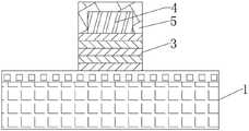
图1为本发明实施例提供的一种堆叠纳米线环栅器件;其制作方法包括如下步骤:Figure 1 is a stacked nanowire gate-all-around device provided by an embodiment of the present invention; its manufacturing method includes the following steps:
步骤1:在SOI(Silicon On Insulator,绝缘层上的硅)片1上通过外延方式依次交叠生长SiGe层202和Si层201,形成堆叠层2;外延的层数可以是一层也可以是多层。Step 1: On the SOI (Silicon On Insulator, silicon on insulating layer) sheet 1, the
如图2所示,Si层201作为沟道层,其层数决定了后续纳米线根数。As shown in FIG. 2 , the
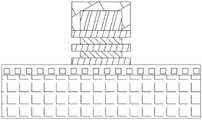
步骤2:通过干法刻蚀工艺实现堆叠的Si/SiGe结构。Step 2: realize the stacked Si/SiGe structure through a dry etching process.
如图3所示,步骤1中得到的样品通过光刻和干法刻蚀定义出Si/SiGe堆叠结构3。As shown in FIG. 3 , the sample obtained in step 1 defines a Si/
步骤3:依次制作假栅4和第一侧墙层5。Step 3: Fabricate the
如图4所示,其中,假栅4采用的材料为多晶硅,第一侧墙层5采用的材料为氧化硅。As shown in FIG. 4 , the material used for the
假栅4定义出后续高K金属栅的位置。The
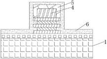
步骤4:通过原子层刻蚀方式刻蚀SiGe层202,形成内凹形貌。Step 4: Etching the
如图5所示,其中,内凹形貌的刻蚀深度与第一侧墙层5厚度一致;内凹深度与第一侧墙层5一致更有利于后续高K金属栅的形成,有利于高K金属栅能淀积的正好环绕Si纳米线沟道。As shown in Figure 5, the etching depth of the concave shape is consistent with the thickness of the
步骤5:淀积第二侧墙层6,填充满刻蚀出的内凹形貌的凹槽形成内侧墙8。Step 5: Deposit the second
如图6所示,淀积第二侧墙层6,且填充满内凹处,第二侧墙层6材料一般为Si3N4。但是并不局限于此,第二侧墙层6材料还可以扩展到SiC,SiN,SiON等。As shown in FIG. 6 , the
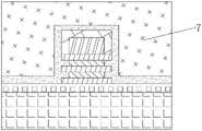
步骤6:在第二侧墙层6上淀积填充层7,平坦化至使第二侧墙层6裸露。Step 6: Deposit a
如图7所示,填充层7的材质可以为SOC(旋涂碳)或者PI(聚酰亚胺)。这两种材料在刻蚀侧墙层时选择比较高,且比较容易通过灰化工艺去除。As shown in FIG. 7 , the material of the
如图8所示,平坦化的方式可以采用回刻或者CMP(chemical mechanicalpolishing,化学机械抛光)直到露出第二侧墙层6。其中,回刻是指整面干法刻蚀。As shown in FIG. 8 , etching back or CMP (chemical mechanical polishing, chemical mechanical polishing) may be used for planarization until the
步骤7:通过干法各向异性刻蚀第二侧墙层6的顶部和侧壁。Step 7: Anisotropically etching the top and sidewalls of the
如图9所示,通过自对准刻蚀方式刻蚀第二侧墙层的顶部和侧壁,仅留下内侧墙8和底部第二侧墙层。As shown in FIG. 9 , the top and sidewalls of the second sidewall layer are etched by self-aligned etching, leaving only the
步骤8:通过灰化工艺去除填充层7,再通过干法各向异性刻蚀去除底部Si3N4材料,仅留下内侧墙8。Step 8: removing the
如图10所示,其中,依次去除填充层7和第二侧墙层底部,形成完整的内侧墙8,且第二侧墙层6的侧壁及底部完全刻蚀。As shown in FIG. 10 , the
灰化工艺为在去胶腔室用比较大的压力100mT~2T,高的氧气流量1000sccm~5000sccm来进行化学反应去除全部的填充层。The ashing process is to use a relatively high pressure of 100mT-2T and a high oxygen flow rate of 1000sccm-5000sccm in the degumming chamber to perform a chemical reaction to remove all the filling layers.
步骤9:通过外延方式生长源区901和漏区902。Step 9: growing the
如图11所示,其中,源区901和漏区902的材质为硅,该源区901和漏区902通过假栅4下方的体硅纳米线外延出来的。As shown in FIG. 11 , the material of the
步骤10:湿法腐蚀去除假栅4和第一侧墙层5。Step 10: removing the
步骤11:释放SiGe层202,形成纳米线沟道。Step 11: releasing the
其中,用HCl气体或者原子层刻蚀方式去除SiGe层202形成Si纳米线沟道。Wherein, the
步骤12:形成环绕纳米线沟道的高K金属栅12;填充绝缘层10,制作接触孔和引线11,完成制备。Step 12: forming a high-
其中,在原假栅形成位置以及SiGe层202释放后的空间填充高K金属,形成环绕纳米线沟道的高K金属栅12。Wherein, the original dummy gate formation position and the released space of the
然后在SOI片1的裸露区域以及源区901、漏区902和高K金属栅12上形成绝缘层10,并在源区901、漏区902和高K金属栅12对应位置形成接触孔,并淀积金属,形成金属引线,得到如图1所示的堆叠纳米线环栅器件。Then an insulating
以上所述的具体实施例,对本发明的目的、技术方案和有益效果进行了进一步详细说明,应理解的是,以上所述仅为本发明的具体实施例而已,并不用于限制本发明,凡在本发明的精神和原则之内,所做的任何修改、等同替换、改进等,均应包含在本发明的保护范围之内。The specific embodiments described above have further described the purpose, technical solutions and beneficial effects of the present invention in detail. It should be understood that the above descriptions are only specific embodiments of the present invention, and are not intended to limit the present invention. Within the spirit and principles of the present invention, any modifications, equivalent replacements, improvements, etc., shall be included in the protection scope of the present invention.
Claims (10)
Translated fromChinesePriority Applications (1)
| Application Number | Priority Date | Filing Date | Title |
|---|---|---|---|
| CN202011036930.4ACN112151386B (en) | 2020-09-27 | 2020-09-27 | Stacked nanowire ring gate device and manufacturing method thereof |
Applications Claiming Priority (1)
| Application Number | Priority Date | Filing Date | Title |
|---|---|---|---|
| CN202011036930.4ACN112151386B (en) | 2020-09-27 | 2020-09-27 | Stacked nanowire ring gate device and manufacturing method thereof |
Publications (2)
| Publication Number | Publication Date |
|---|---|
| CN112151386A CN112151386A (en) | 2020-12-29 |
| CN112151386Btrue CN112151386B (en) | 2023-01-06 |
Family
ID=73895823
Family Applications (1)
| Application Number | Title | Priority Date | Filing Date |
|---|---|---|---|
| CN202011036930.4AActiveCN112151386B (en) | 2020-09-27 | 2020-09-27 | Stacked nanowire ring gate device and manufacturing method thereof |
Country Status (1)
| Country | Link |
|---|---|
| CN (1) | CN112151386B (en) |
Families Citing this family (1)
| Publication number | Priority date | Publication date | Assignee | Title |
|---|---|---|---|---|
| EP4261889A4 (en)* | 2021-01-13 | 2024-03-13 | Huawei Technologies Co., Ltd. | MEMORY, GATE ALL AROUND FIELD EFFECT TRANSISTOR AND MANUFACTURING METHOD |
Citations (14)
| Publication number | Priority date | Publication date | Assignee | Title |
|---|---|---|---|---|
| CN104752185A (en)* | 2013-12-31 | 2015-07-01 | 中芯国际集成电路制造(上海)有限公司 | Forming method of metal grid electrode |
| CN105633004A (en)* | 2014-10-27 | 2016-06-01 | 中国科学院微电子研究所 | Self-Aligned Contact Fabrication Method |
| CN106030815A (en)* | 2014-03-24 | 2016-10-12 | 英特尔公司 | Integrated method for fabricating internal spacers for nanowire devices |
| CN107749421A (en)* | 2017-09-30 | 2018-03-02 | 中国科学院微电子研究所 | Vertically stacked gate-all-around nanowire transistor and preparation method thereof |
| CN107845684A (en)* | 2017-09-30 | 2018-03-27 | 中国科学院微电子研究所 | Vertically stacked gate-all-around nanowire transistor and preparation method thereof |
| CN109216454A (en)* | 2017-07-07 | 2019-01-15 | 中芯国际集成电路制造(北京)有限公司 | Nano-wire transistor and forming method thereof |
| CN109830525A (en)* | 2019-01-25 | 2019-05-31 | 中国科学院微电子研究所 | The production method of nano-wire devices |
| CN110189997A (en)* | 2019-04-28 | 2019-08-30 | 中国科学院微电子研究所 | Stacked nanosheet gate-all-around transistor and preparation method thereof |
| CN110246899A (en)* | 2019-06-05 | 2019-09-17 | 华东师范大学 | A kind of nanometer loop grid field effect transistor with the double-deck sidewall structure |
| CN110277316A (en)* | 2018-03-13 | 2019-09-24 | 中芯国际集成电路制造(上海)有限公司 | Semiconductor structures and methods of forming them |
| TW202009996A (en)* | 2018-08-21 | 2020-03-01 | 美商格芯(美國)集成電路科技有限公司 | Nanosheet field-effect transistors formed with sacrificial spacers |
| CN110938434A (en)* | 2019-12-05 | 2020-03-31 | 中国科学院微电子研究所 | Etching method of inner wall, etching gas and preparation method of nanowire device |
| TW202013729A (en)* | 2018-05-30 | 2020-04-01 | 美商格芯(美國)集成電路科技有限公司 | Forming a surrounding contact with multiple silicide layers |
| CN111490092A (en)* | 2019-01-29 | 2020-08-04 | 中芯国际集成电路制造(北京)有限公司 | Semiconductor structure and method of forming the same |
Family Cites Families (3)
| Publication number | Priority date | Publication date | Assignee | Title |
|---|---|---|---|---|
| CN105336597B (en)* | 2015-10-26 | 2018-05-01 | 上海集成电路研发中心有限公司 | A kind of preparation method of all-around-gate structure |
| US10236362B2 (en)* | 2016-06-30 | 2019-03-19 | International Business Machines Corporation | Nanowire FET including nanowire channel spacers |
| US11289573B2 (en)* | 2019-03-01 | 2022-03-29 | International Business Machines Corporation | Contact resistance reduction in nanosheet device structure |
- 2020
- 2020-09-27CNCN202011036930.4Apatent/CN112151386B/enactiveActive
Patent Citations (14)
| Publication number | Priority date | Publication date | Assignee | Title |
|---|---|---|---|---|
| CN104752185A (en)* | 2013-12-31 | 2015-07-01 | 中芯国际集成电路制造(上海)有限公司 | Forming method of metal grid electrode |
| CN106030815A (en)* | 2014-03-24 | 2016-10-12 | 英特尔公司 | Integrated method for fabricating internal spacers for nanowire devices |
| CN105633004A (en)* | 2014-10-27 | 2016-06-01 | 中国科学院微电子研究所 | Self-Aligned Contact Fabrication Method |
| CN109216454A (en)* | 2017-07-07 | 2019-01-15 | 中芯国际集成电路制造(北京)有限公司 | Nano-wire transistor and forming method thereof |
| CN107749421A (en)* | 2017-09-30 | 2018-03-02 | 中国科学院微电子研究所 | Vertically stacked gate-all-around nanowire transistor and preparation method thereof |
| CN107845684A (en)* | 2017-09-30 | 2018-03-27 | 中国科学院微电子研究所 | Vertically stacked gate-all-around nanowire transistor and preparation method thereof |
| CN110277316A (en)* | 2018-03-13 | 2019-09-24 | 中芯国际集成电路制造(上海)有限公司 | Semiconductor structures and methods of forming them |
| TW202013729A (en)* | 2018-05-30 | 2020-04-01 | 美商格芯(美國)集成電路科技有限公司 | Forming a surrounding contact with multiple silicide layers |
| TW202009996A (en)* | 2018-08-21 | 2020-03-01 | 美商格芯(美國)集成電路科技有限公司 | Nanosheet field-effect transistors formed with sacrificial spacers |
| CN109830525A (en)* | 2019-01-25 | 2019-05-31 | 中国科学院微电子研究所 | The production method of nano-wire devices |
| CN111490092A (en)* | 2019-01-29 | 2020-08-04 | 中芯国际集成电路制造(北京)有限公司 | Semiconductor structure and method of forming the same |
| CN110189997A (en)* | 2019-04-28 | 2019-08-30 | 中国科学院微电子研究所 | Stacked nanosheet gate-all-around transistor and preparation method thereof |
| CN110246899A (en)* | 2019-06-05 | 2019-09-17 | 华东师范大学 | A kind of nanometer loop grid field effect transistor with the double-deck sidewall structure |
| CN110938434A (en)* | 2019-12-05 | 2020-03-31 | 中国科学院微电子研究所 | Etching method of inner wall, etching gas and preparation method of nanowire device |
Also Published As
| Publication number | Publication date |
|---|---|
| CN112151386A (en) | 2020-12-29 |
Similar Documents
| Publication | Publication Date | Title |
|---|---|---|
| CN103839816B (en) | Semiconductor device and method for manufacturing the same | |
| CN110896055B (en) | Preparation method of stacked nanowire or wafer ring gate CMOS (complementary metal oxide semiconductor) device | |
| CN104425284B (en) | Stomata overlying silicon framework of the matrix fin field-effect transistor independent of grid length | |
| US9219129B2 (en) | Inverted thin channel mosfet with self-aligned expanded source/drain | |
| CN103999202B (en) | The semiconductor fin of rare earth oxide isolation | |
| CN102820230A (en) | Fin-last replacement metal gate FinFET | |
| TWI509710B (en) | Semiconductor device with improved gate height uniformity and method of fabricating the same | |
| CN105453264A (en) | Improved silicide formation through improved SiGe faceting | |
| CN107958871B (en) | Semiconductor device and method for manufacturing the same | |
| TW201735178A (en) | Method of forming a semiconductor device | |
| CN111435643B (en) | Preparation method of three-dimensional stacked gate-all-around transistor | |
| CN102468215B (en) | Trench isolation structure and forming method thereof | |
| CN105590856A (en) | Nanowire device manufacturing method | |
| CN115763254A (en) | Stacked nanosheet ring gate transistor and preparation method thereof | |
| CN112151386B (en) | Stacked nanowire ring gate device and manufacturing method thereof | |
| CN111435642B (en) | Three-dimensional stacked semiconductor nanowire structure and preparation method thereof | |
| CN116072542A (en) | Preparation method of ring grid TFET device | |
| CN114203635A (en) | Method for forming a semiconductor device | |
| US10978335B2 (en) | Method for producing a gate cut structure on an array of semiconductor fins | |
| CN104103506B (en) | Semiconductor device manufacturing method | |
| CN103295889B (en) | Fin-shaped active area is prepared the method for high-K metal gate | |
| CN108389786A (en) | The hard mask processing method of memory block manufacturing process for three-dimensional storage part | |
| WO2014109087A1 (en) | Method for manufacturing semiconductor device | |
| CN117116854A (en) | Semiconductor structures and methods of forming them | |
| CN104835738A (en) | Method of forming fins of FinFET device |
Legal Events
| Date | Code | Title | Description |
|---|---|---|---|
| PB01 | Publication | ||
| PB01 | Publication | ||
| SE01 | Entry into force of request for substantive examination | ||
| SE01 | Entry into force of request for substantive examination | ||
| GR01 | Patent grant | ||
| GR01 | Patent grant |