CN112136367A - Flexible printed circuit for skin applications - Google Patents
Flexible printed circuit for skin applicationsDownload PDFInfo
- Publication number
- CN112136367A CN112136367ACN201880093302.4ACN201880093302ACN112136367ACN 112136367 ACN112136367 ACN 112136367ACN 201880093302 ACN201880093302 ACN 201880093302ACN 112136367 ACN112136367 ACN 112136367A
- Authority
- CN
- China
- Prior art keywords
- printed circuit
- flexible printed
- conductive
- synthetic polymer
- skin
- Prior art date
- Legal status (The legal status is an assumption and is not a legal conclusion. Google has not performed a legal analysis and makes no representation as to the accuracy of the status listed.)
- Pending
Links
Images


Classifications
- H—ELECTRICITY
- H05—ELECTRIC TECHNIQUES NOT OTHERWISE PROVIDED FOR
- H05K—PRINTED CIRCUITS; CASINGS OR CONSTRUCTIONAL DETAILS OF ELECTRIC APPARATUS; MANUFACTURE OF ASSEMBLAGES OF ELECTRICAL COMPONENTS
- H05K1/00—Printed circuits
- H05K1/02—Details
- H05K1/0277—Bendability or stretchability details
- H05K1/0283—Stretchable printed circuits
- H—ELECTRICITY
- H05—ELECTRIC TECHNIQUES NOT OTHERWISE PROVIDED FOR
- H05K—PRINTED CIRCUITS; CASINGS OR CONSTRUCTIONAL DETAILS OF ELECTRIC APPARATUS; MANUFACTURE OF ASSEMBLAGES OF ELECTRICAL COMPONENTS
- H05K1/00—Printed circuits
- H05K1/02—Details
- H05K1/03—Use of materials for the substrate
- H05K1/0393—Flexible materials
- H—ELECTRICITY
- H05—ELECTRIC TECHNIQUES NOT OTHERWISE PROVIDED FOR
- H05K—PRINTED CIRCUITS; CASINGS OR CONSTRUCTIONAL DETAILS OF ELECTRIC APPARATUS; MANUFACTURE OF ASSEMBLAGES OF ELECTRICAL COMPONENTS
- H05K1/00—Printed circuits
- H05K1/02—Details
- H05K1/0277—Bendability or stretchability details
- H05K1/028—Bending or folding regions of flexible printed circuits
- H—ELECTRICITY
- H05—ELECTRIC TECHNIQUES NOT OTHERWISE PROVIDED FOR
- H05K—PRINTED CIRCUITS; CASINGS OR CONSTRUCTIONAL DETAILS OF ELECTRIC APPARATUS; MANUFACTURE OF ASSEMBLAGES OF ELECTRICAL COMPONENTS
- H05K1/00—Printed circuits
- H05K1/02—Details
- H05K1/03—Use of materials for the substrate
- H05K1/0313—Organic insulating material
- H—ELECTRICITY
- H05—ELECTRIC TECHNIQUES NOT OTHERWISE PROVIDED FOR
- H05K—PRINTED CIRCUITS; CASINGS OR CONSTRUCTIONAL DETAILS OF ELECTRIC APPARATUS; MANUFACTURE OF ASSEMBLAGES OF ELECTRICAL COMPONENTS
- H05K1/00—Printed circuits
- H05K1/02—Details
- H05K1/09—Use of materials for the conductive, e.g. metallic pattern
- H05K1/092—Dispersed materials, e.g. conductive pastes or inks
- H05K1/097—Inks comprising nanoparticles and specially adapted for being sintered at low temperature
- H—ELECTRICITY
- H05—ELECTRIC TECHNIQUES NOT OTHERWISE PROVIDED FOR
- H05K—PRINTED CIRCUITS; CASINGS OR CONSTRUCTIONAL DETAILS OF ELECTRIC APPARATUS; MANUFACTURE OF ASSEMBLAGES OF ELECTRICAL COMPONENTS
- H05K1/00—Printed circuits
- H05K1/02—Details
- H05K1/11—Printed elements for providing electric connections to or between printed circuits
- H05K1/118—Printed elements for providing electric connections to or between printed circuits specially for flexible printed circuits, e.g. using folded portions
- H—ELECTRICITY
- H05—ELECTRIC TECHNIQUES NOT OTHERWISE PROVIDED FOR
- H05K—PRINTED CIRCUITS; CASINGS OR CONSTRUCTIONAL DETAILS OF ELECTRIC APPARATUS; MANUFACTURE OF ASSEMBLAGES OF ELECTRICAL COMPONENTS
- H05K1/00—Printed circuits
- H05K1/18—Printed circuits structurally associated with non-printed electric components
- H05K1/189—Printed circuits structurally associated with non-printed electric components characterised by the use of a flexible or folded printed circuit
- H—ELECTRICITY
- H05—ELECTRIC TECHNIQUES NOT OTHERWISE PROVIDED FOR
- H05K—PRINTED CIRCUITS; CASINGS OR CONSTRUCTIONAL DETAILS OF ELECTRIC APPARATUS; MANUFACTURE OF ASSEMBLAGES OF ELECTRICAL COMPONENTS
- H05K3/00—Apparatus or processes for manufacturing printed circuits
- H05K3/40—Forming printed elements for providing electric connections to or between printed circuits
- H05K3/4038—Through-connections; Vertical interconnect access [VIA] connections
- A—HUMAN NECESSITIES
- A61—MEDICAL OR VETERINARY SCIENCE; HYGIENE
- A61B—DIAGNOSIS; SURGERY; IDENTIFICATION
- A61B2562/00—Details of sensors; Constructional details of sensor housings or probes; Accessories for sensors
- A61B2562/16—Details of sensor housings or probes; Details of structural supports for sensors
- A61B2562/166—Details of sensor housings or probes; Details of structural supports for sensors the sensor is mounted on a specially adapted printed circuit board
- H—ELECTRICITY
- H05—ELECTRIC TECHNIQUES NOT OTHERWISE PROVIDED FOR
- H05K—PRINTED CIRCUITS; CASINGS OR CONSTRUCTIONAL DETAILS OF ELECTRIC APPARATUS; MANUFACTURE OF ASSEMBLAGES OF ELECTRICAL COMPONENTS
- H05K2201/00—Indexing scheme relating to printed circuits covered by H05K1/00
- H05K2201/01—Dielectrics
- H05K2201/0104—Properties and characteristics in general
- H05K2201/0116—Porous, e.g. foam
- H—ELECTRICITY
- H05—ELECTRIC TECHNIQUES NOT OTHERWISE PROVIDED FOR
- H05K—PRINTED CIRCUITS; CASINGS OR CONSTRUCTIONAL DETAILS OF ELECTRIC APPARATUS; MANUFACTURE OF ASSEMBLAGES OF ELECTRICAL COMPONENTS
- H05K2201/00—Indexing scheme relating to printed circuits covered by H05K1/00
- H05K2201/01—Dielectrics
- H05K2201/0137—Materials
- H05K2201/015—Fluoropolymer, e.g. polytetrafluoroethylene [PTFE]
Landscapes
- Engineering & Computer Science (AREA)
- Microelectronics & Electronic Packaging (AREA)
- Chemical & Material Sciences (AREA)
- Nanotechnology (AREA)
- Dispersion Chemistry (AREA)
- Manufacturing & Machinery (AREA)
- Laminated Bodies (AREA)
- Structure Of Printed Boards (AREA)
- Non-Metallic Protective Coatings For Printed Circuits (AREA)
Abstract
Translated fromChinese
Description
Translated fromChinese技术领域technical field
本公开一般涉及柔性印刷电路,更具体地,涉及经皮施用并且长时间舒适的柔性印刷电路,柔性电路板和混合柔性电路板。The present disclosure relates generally to flexible printed circuits, and more particularly, to flexible printed circuits, flexible circuit boards, and hybrid flexible circuit boards that are applied transdermally and are comfortable for extended periods of time.
背景技术Background technique
传统上,柔性电路是建立在诸如Mylar或
在这方面,已经开发出许多薄且可拉伸的导电油墨。这些油墨通常直接印刷在纺织品上,并且能够保持纺织品的柔性,可拉伸性和手感。然而,它们遭受明显的耐久性和电连接性问题。例如,当纺织品被拉伸时,纺织品纤维束相对于彼此显著移动。导电油墨不能承受弥合纺织纤维束之间的间隙所需的伸长,从而导致断裂和开路。In this regard, a number of thin and stretchable conductive inks have been developed. These inks are usually printed directly on textiles and maintain the flexibility, stretchability and feel of the textiles. However, they suffer from significant durability and electrical connectivity issues. For example, when the textile is stretched, the textile fiber bundles move significantly relative to each other. Conductive inks cannot withstand the elongation required to bridge the gaps between textile fiber bundles, resulting in breaks and open circuits.
相同的可拉伸导电油墨已印刷到聚氨酯膜上,然后热粘合到拉伸纺织品上。与直接印刷到纺织品上相比,这导致电路更耐用,但是所得层压件的拉伸度明显小于原始纺织品。在其他现有技术中,导电油墨已经被夹在绝缘油墨之间,然后被热层压到纺织品上。但是,绝缘油墨的薄涂层不能有效地支撑导电油墨。增加绝缘油墨的厚度可以提高耐久性,但是会大大降低纺织品的可拉伸性。The same stretchable conductive ink has been printed onto a polyurethane film and then thermally bonded to the stretched textile. This resulted in a more durable circuit than printing directly onto the textile, but the resulting laminate stretched significantly less than the original textile. In other prior art, conductive inks have been sandwiched between insulating inks and then thermally laminated to textiles. However, thin coatings of insulating inks cannot effectively support conductive inks. Increasing the thickness of the insulating ink improves durability, but greatly reduces the stretchability of the textile.
尽管柔性电路取得了进步,但是仍然需要用于从服装到医疗诊断和治疗设备以及许多其他合适的最终应用的各种应用的耐久且有效的柔性电路系统。Despite the advances in flexible circuits, there remains a need for durable and efficient flexible circuit systems for a variety of applications ranging from apparel to medical diagnostic and therapeutic devices and many other suitable end applications.
发明内容SUMMARY OF THE INVENTION
一个实施方式涉及柔性印刷电路,该柔性印刷电路包括:(1)具有结点和原纤维微结构以及第一和第二表面的微孔合成聚合物膜,(2)位于微孔合成聚合物膜的第一和/或第二表面上的至少一条导电迹线,和(3)位于微孔合成聚合物膜的第一和/或第二表面上的皮肤可接受的粘合剂。微孔合成聚合物膜可以是膨胀聚四氟乙烯膜。在至少一个实施方式中,导电迹线位于合成聚合物膜的第一表面上,而皮肤可接受的粘合剂位于合成聚合物膜的第二表面上。在一些实施方式中,导电迹线可以位于合成聚合物膜的第一和第二表面上,并且皮肤可接受的粘合剂位于合成聚合物膜的第一和第二表面中的至少一个上。在一些实施方式中,吸收的导电迹线使第一表面上的导电迹线与第二表面上的导电迹线电互连。绝缘外涂层可以位于导电迹线的至少一部分上。导电迹线可以是银,铂,金,铜,炭黑及其组合的颗粒或纳米颗粒。另外,导电迹线可以包括导电颗粒的连续网络。导电迹线可以具有导电图案或电路的形式。柔性电路的柔度值小于约1.0牛顿,如峰值压缩载荷测试(压缩屈曲)的测试方法所证明的。同样,当根据电阻翻倍所需载荷测试方法进行测试时,导致电阻2倍增加所施加的载荷大于约0.7牛顿。One embodiment relates to a flexible printed circuit comprising: (1) a microporous synthetic polymer membrane having a junction and fibril microstructure and first and second surfaces, (2) on the microporous synthetic polymer membrane at least one conductive trace on the first and/or second surface of the microporous synthetic polymer film, and (3) a skin-acceptable adhesive on the first and/or second surface of the microporous synthetic polymer film. The microporous synthetic polymer membrane may be an expanded polytetrafluoroethylene membrane. In at least one embodiment, the conductive traces are on a first surface of the synthetic polymer film and the skin-acceptable adhesive is on a second surface of the synthetic polymer film. In some embodiments, the conductive traces may be located on the first and second surfaces of the synthetic polymer film, and the skin-acceptable adhesive is located on at least one of the first and second surfaces of the synthetic polymer film. In some embodiments, the absorbed conductive traces electrically interconnect the conductive traces on the first surface with the conductive traces on the second surface. An insulating overcoat may be located on at least a portion of the conductive traces. The conductive traces can be particles or nanoparticles of silver, platinum, gold, copper, carbon black, and combinations thereof. Additionally, the conductive traces may comprise a continuous network of conductive particles. The conductive traces may be in the form of conductive patterns or circuits. The flex circuit has a compliance value of less than about 1.0 Newton, as evidenced by the test method of the Peak Compressive Load Test (Compression Buckling). Likewise, when tested according to the load required to double the resistance test method, the applied load resulting in a 2-fold increase in resistance was greater than about 0.7 Newtons.
柔性印刷电路可以进一步包括至少一个电子部件以形成柔性电路板。电子部件可以包括电子电阻器,电容器,发光二极管(LED),集成电路,传感器,电源,数据发送器,数据接收器及其组合。The flexible printed circuit may further include at least one electronic component to form a flexible circuit board. Electronic components may include electronic resistors, capacitors, light emitting diodes (LEDs), integrated circuits, sensors, power supplies, data transmitters, data receivers, and combinations thereof.
柔性电路或柔性电路板可以与电子模块结合以形成混合柔性印刷电路板。在一些实施方式中,电子模块可以与导电迹线位于微孔合成聚合物膜的同一侧。在另一个实施方式中,电子模块可以被构造成定位在微孔合成聚合物膜和使用者皮肤之间。Flexible circuits or flexible circuit boards can be combined with electronic modules to form hybrid flexible printed circuit boards. In some embodiments, the electronic module may be located on the same side of the microporous synthetic polymer membrane as the conductive traces. In another embodiment, the electronic module may be configured to be positioned between the microporous synthetic polymer membrane and the user's skin.
另一实施方式涉及柔性印刷电路,其包括:(1)微孔合成聚合物膜,(2)位于微孔合成聚合物膜内的至少一条导电迹线,以及(3)位于合成聚合物膜上的皮肤可接受的粘合剂。在一些实施方式中,导电迹线沿着微孔合成聚合物膜的厚度填充孔。微孔合成聚合物膜可以是膨胀聚四氟乙烯膜。导电迹线可以是银,铂,金,铜,炭黑及其组合的颗粒或纳米颗粒。另外,导电迹线可以包括导电颗粒的连续网络。导电迹线可以具有导电图案或电路的形式。柔性电路的柔度值小于约1.0牛顿,如峰值压缩载荷测试(压缩屈曲)的测试方法所证明的。同样,当根据电阻翻倍所需载荷测试方法进行测试时,导致电阻2倍增加所施加的载荷大于约0.7牛顿。Another embodiment relates to a flexible printed circuit comprising: (1) a microporous synthetic polymer film, (2) at least one conductive trace within the microporous synthetic polymer film, and (3) on the synthetic polymer film skin-acceptable adhesive. In some embodiments, the conductive traces fill the pores along the thickness of the microporous synthetic polymer film. The microporous synthetic polymer membrane may be an expanded polytetrafluoroethylene membrane. The conductive traces can be particles or nanoparticles of silver, platinum, gold, copper, carbon black, and combinations thereof. Additionally, the conductive traces may comprise a continuous network of conductive particles. The conductive traces may be in the form of conductive patterns or circuits. The flex circuit has a compliance value of less than about 1.0 Newton, as evidenced by the test method of the Peak Compressive Load Test (Compression Buckling). Likewise, when tested according to the load required to double the resistance test method, the applied load resulting in a 2-fold increase in resistance was greater than about 0.7 Newtons.
柔性印刷电路可以进一步包括至少一个电子部件以形成柔性电路板。电子部件可以包括电子电阻器,电容器,发光二极管(LED),集成电路,传感器,电源,数据发送器,数据接收器及其组合。The flexible printed circuit may further include at least one electronic component to form a flexible circuit board. Electronic components may include electronic resistors, capacitors, light emitting diodes (LEDs), integrated circuits, sensors, power supplies, data transmitters, data receivers, and combinations thereof.
柔性电路或柔性电路板可以与电子模块结合以形成混合柔性印刷电路板。在一些实施方式中,电子模块可以与导电迹线位于微孔合成聚合物膜的同一侧。在另一个实施方式中,电子模块可以被构造成定位在微孔合成聚合物膜和使用者皮肤之间。Flexible circuits or flexible circuit boards can be combined with electronic modules to form hybrid flexible printed circuit boards. In some embodiments, the electronic module may be located on the same side of the microporous synthetic polymer membrane as the conductive traces. In another embodiment, the electronic module may be configured to be positioned between the microporous synthetic polymer membrane and the user's skin.
附图说明Description of drawings
包括附图以提供对本公开的进一步理解,附图被并入本说明书中并构成本说明书的一部分,附图示出了实施方式,并且与说明书一起用于解释本公开的原理。The accompanying drawings, which are included to provide a further understanding of the disclosure, are incorporated in and constitute a part of this specification, illustrate embodiments, and together with the description serve to explain the principles of the disclosure.
图1是根据至少一个实施方式的微孔膨胀聚四氟乙烯(ePTFE)膜(膜1)的扫描电子显微镜(SEM)图像;1 is a scanning electron microscope (SEM) image of a microporous expanded polytetrafluoroethylene (ePTFE) membrane (Membrane 1) in accordance with at least one embodiment;
图2是根据至少一个实施方式的微孔膨胀聚四氟乙烯(ePTFE)膜(膜2)的SEM图像;2 is an SEM image of a microporous expanded polytetrafluoroethylene (ePTFE) membrane (Membrane 2) in accordance with at least one embodiment;
图3是在根据至少一个实施方式的实施例4中使用的微孔聚乙烯锂离子电池绝缘膜的SEM图像;3 is an SEM image of a microporous polyethylene lithium-ion battery insulating film used in Example 4 in accordance with at least one embodiment;
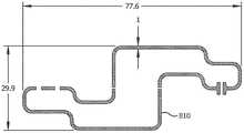
图4是在根据至少一个实施方式的实例中使用的示例性导电迹线的布置和尺寸的图示;4 is an illustration of the arrangement and dimensions of exemplary conductive traces used in an example in accordance with at least one embodiment;
图5是描绘根据至少一个实施方式的在舒适度测试期间施加到肘部的内表面的柔性印刷电路板的位置的示意图;5 is a schematic diagram depicting the position of a flexible printed circuit board applied to the inner surface of an elbow during a comfort test in accordance with at least one embodiment;
图6是根据至少一个实施方式的在名为“峰值压缩载荷测试(压缩屈曲)”的测试方法中使用的压缩测试装置的示意图;6 is a schematic diagram of a compression testing apparatus used in a test method named "Peak Compression Load Testing (Compression Buckling)" in accordance with at least one embodiment;
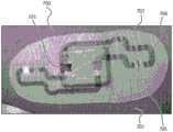
图7是根据至少一个实施方式的用于皮肤应用的示例性混合柔性印刷电路板的图像;7 is an image of an exemplary hybrid flexible printed circuit board for skin application in accordance with at least one embodiment;
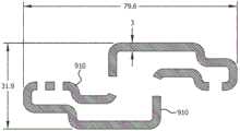
图8是根据至少一个实施方式的在实施例8中印刷在ePTFE膜上的导电油墨的印刷图案的示意图;8 is a schematic illustration of a printed pattern of conductive ink printed on an ePTFE membrane in Example 8, according to at least one embodiment;
图9是根据至少一个实施方式的施加在如图8所示且如实施例8中描述的大部分印刷图案上的绝缘外涂层的示意图;9 is a schematic diagram of an insulating overcoat applied over a majority of the printed pattern shown in FIG. 8 and as described in Example 8, in accordance with at least one embodiment;
图10是根据至少一个实施方式的具有使用导电油墨如实施例8所述粘附到ePTFE膜上的表面安装发光二极管的印刷电路板的示意图;10 is a schematic diagram of a printed circuit board having surface mount light emitting diodes adhered to an ePTFE film using conductive ink as described in Example 8, in accordance with at least one embodiment;
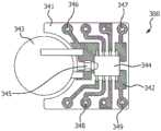
图11是根据至少一个实施方式的电子模块的示意图,该电子模块具有焊接到图案化的铜迹线上的锂电池,处理器和电容器,如实施例8所述;11 is a schematic diagram of an electronic module having a lithium battery, a processor, and a capacitor soldered to patterned copper traces, as described in Example 8, in accordance with at least one embodiment;
图12示出了根据至少一个实施方式的如实施例8所述的由聚碳酸酯加工的两部分壳体,壁厚为约0.3mm,外部尺寸为约25.2mm×19.4mm×4mm;12 illustrates a two-part housing machined from polycarbonate as described in Example 8, having a wall thickness of about 0.3 mm and external dimensions of about 25.2 mm x 19.4 mm x 4 mm, according to at least one embodiment;
图13是根据至少一个实施方式的印刷在图12所示的壳体上的导电油墨图案的示意图,该壳体是用于制造实施例8中所述的电子模块;13 is a schematic diagram of a conductive ink pattern printed on the housing shown in FIG. 12 for use in making the electronic module described in Example 8, in accordance with at least one embodiment;
图14A是根据至少一个实施方式的在其上具有导电迹线和不连续粘合剂的柔性印刷电路的示意图;14A is a schematic diagram of a flexible printed circuit having conductive traces and discontinuous adhesive thereon in accordance with at least one embodiment;
图14B是根据至少一个实施方式的在其内具有导电迹线和不连续粘合剂的柔性印刷电路的示意图;14B is a schematic diagram of a flexible printed circuit having conductive traces and discontinuous adhesive therein in accordance with at least one embodiment;
图14C是根据至少一个实施方式的在合成聚合物膜的两侧上均具有导电迹线的柔性印刷电路的示意图;14C is a schematic diagram of a flexible printed circuit having conductive traces on both sides of a synthetic polymer film in accordance with at least one embodiment;
图14D是根据至少一个实施方式的具有皮肤可接受的粘合剂的柔性印刷电路的示意图,该粘合剂覆盖了一些导电迹线;14D is a schematic diagram of a flexible printed circuit having a skin-acceptable adhesive covering some conductive traces in accordance with at least one embodiment;
图15是根据至少一个实施方式的当人对象的手臂伸开时放置在手臂的弯曲处的柔性印刷电路的图像;15 is an image of a flexible printed circuit placed at a bend of a human subject's arm when the arm is extended, according to at least one embodiment;
图16是根据至少一个实施方式的图15的柔性电路处于略微弯曲的构造的图像,其示出了通过压缩和起皱使柔性印刷电路顺应皮肤;16 is an image of the flexible circuit of FIG. 15 in a slightly curved configuration showing the flexible printed circuit conforming to the skin by compression and wrinkling, according to at least one embodiment;
图17A是根据至少一个实施方式的在使用激光千分尺时,在激光千分尺源和激光千分尺接收器之间对齐的金属圆筒的示意图,该金属圆筒用于测量合成聚合物膜的厚度;和17A is a schematic diagram of a metal cylinder aligned between a laser micrometer source and a laser micrometer receiver for measuring the thickness of a synthetic polymer film when a laser micrometer is used, in accordance with at least one embodiment; and
图17B是根据至少一个实施方式的覆盖在图12A所示的金属圆筒的表面上的单层膜的示意图,当使用激光千分尺测量合成高分子膜的厚度时,该单层膜没有重叠且没有褶皱。17B is a schematic illustration of a monolayer film overlying the surface of the metal cylinder shown in FIG. 12A without overlapping and without the thickness of the synthetic polymer film when measured using a laser micrometer in accordance with at least one embodiment folds.
具体实施方式Detailed ways
本领域的技术人员应理解,可通过构造用于执行目标功能的任何数量的方法和设备来实现本公开内容的各个方面。还应注意,本文参考的附图不一定是按比例绘制,而是有可能放大以说明本公开的各个方面,就此而言,附图不应视为限制性的。应当理解,术语“导电性迹线”,“导电迹线”和“迹线”在本文中可以互换使用。术语“膜”和“薄膜”在本文中可以互换使用。如本文所用,术语“合成聚合物膜”和“微孔合成聚合物膜”可以在本文中互换使用。Those skilled in the art will understand that various aspects of the present disclosure may be implemented by any number of methods and apparatus configured to perform the target functions. It should also be noted that the drawings referred to herein are not necessarily to scale, but may be exaggerated to illustrate various aspects of the present disclosure, and in this regard should not be considered limiting. It should be understood that the terms "conductive trace," "conductive trace," and "trace" are used interchangeably herein. The terms "film" and "film" are used interchangeably herein. As used herein, the terms "synthetic polymer membrane" and "microporous synthetic polymer membrane" may be used interchangeably herein.
本发明涉及用于皮肤应用的柔性印刷电路,其包括微孔合成聚合物膜和至少一条导电迹线。可以将导电迹线吸入或以其他方式引入孔中并穿过微孔合成聚合物膜的厚度,以形成柔性印刷电路。在另一些实施方式中,导电迹线可以位于微孔合成聚合物膜的表面上以形成柔性印刷电路。柔性印刷电路可以电耦合和/或粘附至电子模块,并且通过皮肤可接受的粘合剂粘附至皮肤,例如人皮肤。可以通过施加不连续或连续的粘合剂来进行粘合。另外,柔性印刷电路可以具有电耦合到其上的电子部件以创建柔性印刷电路板。电子模块(例如,传统电路板)可以耦合到柔性印刷电路或柔性印刷电路板以创建混合柔性印刷电路板。The present invention relates to flexible printed circuits for skin applications comprising a microporous synthetic polymer film and at least one conductive trace. Conductive traces can be drawn or otherwise introduced into holes and through the thickness of the microporous synthetic polymer film to form flexible printed circuits. In other embodiments, conductive traces may be located on the surface of the microporous synthetic polymer film to form a flexible printed circuit. The flexible printed circuit can be electrically coupled and/or adhered to the electronic module, and adhered to the skin, eg, human skin, by a skin-acceptable adhesive. Bonding can be done by applying a discontinuous or continuous adhesive. Additionally, a flexible printed circuit may have electronic components electrically coupled thereto to create a flexible printed circuit board. Electronic modules (eg, conventional circuit boards) can be coupled to a flexible printed circuit or a flexible printed circuit board to create a hybrid flexible printed circuit board.
如上所述,柔性印刷电路包括至少一条导电迹线和合成聚合物膜。如本文所用,术语“导电迹线”旨在描述能够传导电子从中通过的连续线或连续路径。在示例性实施方式中,非导电区域位于合成聚合物膜上或之内的导电迹线旁边。在一些实施方式中,可使用导电油墨将导电迹线沉积在合成聚合物膜上或合成聚合物膜内。如本文所用,术语“导电油墨”是指在载液(例如溶剂)中掺入导电颗粒的材料。在一些实施方式中,导电颗粒包括银,金,铜或铂颗粒。合适的导电油墨的非限制性示例包括2108-IPA(Nanogap公司,加利福尼亚州里士满),PE872(杜邦(DuPont),特拉华州威明顿),CI1036(工程导电材料公司(Engineered Conductive Materials),俄亥俄州特拉华)和125-19FS(创新材料公司(Creative Materials,Inc.),马萨诸塞州艾尔)。As mentioned above, the flexible printed circuit includes at least one conductive trace and a synthetic polymer film. As used herein, the term "conductive trace" is intended to describe a continuous line or continuous path through which electrons can be conducted. In an exemplary embodiment, the non-conductive regions are located next to conductive traces on or within the synthetic polymer film. In some embodiments, conductive traces can be deposited on or within a synthetic polymer film using a conductive ink. As used herein, the term "conductive ink" refers to a material incorporating conductive particles in a carrier liquid (eg, a solvent). In some embodiments, the conductive particles include silver, gold, copper or platinum particles. Non-limiting examples of suitable conductive inks include 2108-IPA (Nanogap Corporation, Richmond, CA), PE872 (DuPont, Wilmington, DE), CI1036 (Engineered Conductive Materials) ), Delaware, OH) and 125-19FS (Creative Materials, Inc., Ayr, MA).
形成导电迹线的其他导电材料的非限制性示例包括导电金属颗粒或纳米颗粒(例如,银,金,铜和铂),其他导电材料(例如石墨或炭黑)的颗粒或纳米颗粒),导电纳米管,导电金属薄片,导电聚合物,导电颗粒及其组合。如本文所用,术语“纳米颗粒”旨在描述在导电颗粒的至少一个维度上具有1.0nm至100nm的尺寸的颗粒。Non-limiting examples of other conductive materials that form conductive traces include conductive metal particles or nanoparticles (eg, silver, gold, copper, and platinum), particles or nanoparticles of other conductive materials (eg, graphite or carbon black), conductive Nanotubes, conductive metal flakes, conductive polymers, conductive particles, and combinations thereof. As used herein, the term "nanoparticles" is intended to describe particles having a size of 1.0 nm to 100 nm in at least one dimension of the conductive particles.
导电迹线可以呈导电图案的形式,其可以用于形成电流可以流过的电路。该图案可以创建开放路径,例如图4中例示的平行线或图8所示的图案。在一些实施方式中,电子部件(例如,电阻器,电容器,发光二极管(LED),集成电路,传感器,电源,数据发送器和/或数据接收器)可以电耦合(例如粘附)到柔性印刷电路(例如,图10中所示的导电迹线图案)以创建可以在皮肤上定位的柔性电路板。如本文所用,短语“在皮肤上定位”或“在皮肤上粘附”意在表示将柔性印刷电路或柔性印刷电路板施加到人或动物的皮肤上。例如,柔性印刷电路和柔性印刷电路板可用于向用户或用户的医生传输信息,例如用户的心率或血液中的氧饱和度。The conductive traces can be in the form of conductive patterns, which can be used to form circuits through which electrical current can flow. This pattern can create open paths, such as the parallel lines illustrated in Figure 4 or the pattern shown in Figure 8. In some embodiments, electronic components (eg, resistors, capacitors, light emitting diodes (LEDs), integrated circuits, sensors, power supplies, data transmitters and/or data receivers) can be electrically coupled (eg, adhered) to the flex print circuit (eg, the pattern of conductive traces shown in Figure 10) to create a flexible circuit board that can be positioned on the skin. As used herein, the phrases "locating on the skin" or "adhering to the skin" are intended to mean the application of a flexible printed circuit or flexible printed circuit board to the skin of a human or animal. For example, flexible printed circuits and flexible printed circuit boards can be used to transmit information to the user or the user's physician, such as the user's heart rate or oxygen saturation in the blood.
在至少一个实施方式中,合成聚合物膜是微孔合成聚合物膜或微孔含氟聚合物膜,其具有结点和原纤维微结构,其中结点通过原纤维相互连接,并且孔是整个膜中位于结点和原纤维之间的空隙或空间,例如膨胀聚四氟乙烯(ePTFE)。戈尔(Gore)的美国专利第3,953,566号中描述了示例性的结点和原纤维微结构。In at least one embodiment, the synthetic polymer membrane is a microporous synthetic polymer membrane or a microporous fluoropolymer membrane having a microstructure of nodes and fibrils, wherein the nodes are interconnected by fibrils and the pores are throughout The voids or spaces in a membrane, such as expanded polytetrafluoroethylene (ePTFE), between nodes and fibrils. Exemplary node and fibril microstructures are described in US Patent No. 3,953,566 to Gore.
本文所述的微孔合成聚合物膜可以与其他膜或结构相区别,区别在于它们的比表面积大于约4.0m2/cm3,大于约10m2/cm3,大于约50m2/cm3,大于约75m2/cm3,以及最高至100m2/cm3。在一些实施方式中,比表面积为约4.0m2/cm3至100m2/cm3。在此,比表面积是基于骨架体积而不是包络体积(envelope volume)来定义的。另外,微孔合成聚合物膜中的大多数原纤维的直径小于约1.0μm,或约0.1μm至约1.0μm,约0.3μm至约1.0μm,约0.5μm至约1.0μm,或约0.7μm至约1.0μm。在至少一个示例性实施方式中,合成聚合物膜是膨胀聚四氟乙烯(ePTFE)膜。根据Gore的美国专利第3,953,566号,Bowen等人的美国专利公开第2004/0173978号,Bacino等人的美国专利第7,306,729号中,Bacino的美国专利第5476589号或Branca等人的美国专利第5183545号中描述的方法制备的膨胀聚四氟乙烯(ePTFE)膜可以在本文中使用。另外,微孔合成聚合物膜很薄,厚度小于约100μm,小于约75μm,小于约50μm,小于约35μm,小于约25μm,小于约20μm,小于约10μm,小于约5μm或小于约3μm。The microporous synthetic polymer membranes described herein can be distinguished from other membranes or structures by their specific surface area greater than about 4.0 m2 /cm3 , greater than about 10 m2 /cm3 , greater than about 50 m2 /cm3 , Greater than about 75 m2 /cm3 and up to 100 m2 /cm3 . In some embodiments, the specific surface area is about 4.0 m2 /cm3 to 100 m2 /cm3 . Here, the specific surface area is defined based on the skeleton volume rather than the envelope volume. Additionally, the diameter of the majority of the fibrils in the microporous synthetic polymer film is less than about 1.0 μm, or about 0.1 μm to about 1.0 μm, about 0.3 μm to about 1.0 μm, about 0.5 μm to about 1.0 μm, or about 0.7 μm to about 1.0 μm. In at least one exemplary embodiment, the synthetic polymer membrane is an expanded polytetrafluoroethylene (ePTFE) membrane. According to US Patent No. 3,953,566 to Gore, US Patent Publication No. 2004/0173978 to Bowen et al., US Patent No. 7,306,729 to Bacino et al., US Patent No. 5,476,589 to Bacino, or US Patent No. 5,183,545 to Branca et al. Expanded polytetrafluoroethylene (ePTFE) membranes prepared by the methods described in can be used herein. Additionally, the microporous synthetic polymer films are thin, less than about 100 μm, less than about 75 μm, less than about 50 μm, less than about 35 μm, less than about 25 μm, less than about 20 μm, less than about 10 μm, less than about 5 μm, or less than about 3 μm thick.
在一个实施方式中,导电迹线可以施加于合成聚合物膜的外表面以形成柔性印刷电路。在至少一个实施方式中,将具有所需图案的模板施加到合成聚合物膜的表面上。本领域技术人员已知的在微孔合成聚合物膜的表面上形成图案的其他形式被认为在本公开的范围内。在示例性实施方式中,合成聚合物膜是平坦的(即,平面的),并且在施加导电材料时不包含皱纹。将导电材料(例如,导电油墨)施加到模板上,使得一旦去除模板,导电材料就以期望的图案保留在合成聚合物膜上,从而形成导电迹线。可以施加导电材料,使得导电迹线位于合成聚合物膜的外表面的至少一部分上以形成柔性印刷电路。应当理解,本文所使用的关于导电迹线的术语“在......上”是指该迹线在合成聚合物膜的表面上(即,没有导电材料位于合成聚合物膜的孔中)或者迹线基本上位于合成聚合物膜的表面上(即,可忽略量的导电材料可以位于合成聚合物膜的孔中)。“在......上”还意味着表示导电迹线可以直接定位在基材上(没有中间元件),或者可以存在中间元件。尽管不希望受到理论的束缚,但据信,导电材料向微孔合成聚合物膜的孔中的微不足道的渗透(例如,微米)会导致导电迹线对合成聚合物膜表面的改善的粘附。In one embodiment, conductive traces may be applied to the outer surface of the synthetic polymer film to form a flexible printed circuit. In at least one embodiment, a template having the desired pattern is applied to the surface of the synthetic polymer film. Other forms of patterning on the surface of a microporous synthetic polymer membrane known to those skilled in the art are considered to be within the scope of the present disclosure. In an exemplary embodiment, the synthetic polymer film is flat (ie, planar) and contains no wrinkles when the conductive material is applied. A conductive material (eg, a conductive ink) is applied to the template such that once the template is removed, the conductive material remains on the synthetic polymer film in a desired pattern, thereby forming conductive traces. The conductive material can be applied such that conductive traces are located on at least a portion of the outer surface of the synthetic polymer film to form a flexible printed circuit. It should be understood that the term "on" as used herein with respect to a conductive trace means that the trace is on the surface of the synthetic polymer film (ie, no conductive material is located in the pores of the synthetic polymer film ) or the traces are located substantially on the surface of the synthetic polymer film (ie, a negligible amount of conductive material may be located in the pores of the synthetic polymer film). "On" is also meant to mean that the conductive traces may be positioned directly on the substrate (without intervening elements), or intervening elements may be present. While not wishing to be bound by theory, it is believed that insignificant penetration (eg, micrometers) of the conductive material into the pores of the microporous synthetic polymer membrane results in improved adhesion of the conductive traces to the synthetic polymer membrane surface.
在另一个实施方式中,可将导电材料(例如,导电油墨)施加到合成聚合物膜上,使得导电材料被吸入或以其他方式结合到微孔合成聚合物膜中,从而将导电材料,继而导电迹线设置在微孔合成聚合物膜内,从而形成柔性印刷电路。如本文所用,“吸收/吸入”意在描述导电材料通常通过液体载体(例如导电油墨)纳入和/或沉积到微孔合成聚合物膜的现有孔或空隙中,并且特别排除了其中导电迹线是合成聚合物膜的组成部分的填充膜,其在孔或空隙空间内可能有一些暴露的导电迹线。要注意的是,本文中可以使用将导电材料沉积到膜的孔或空隙空间中的任何已知方法。在一些实施方式中,导电迹线沿着微孔合成聚合物膜的厚度占据孔。这样,导电迹线可占据微孔合成聚合物膜中的大部分孔体积。在示例性实施方式中,孔包含一定量的导电材料,该量足以产生用于电子通过的导电迹线。In another embodiment, a conductive material (eg, a conductive ink) can be applied to the synthetic polymer film such that the conductive material is imbibed or otherwise incorporated into the microporous synthetic polymer film, thereby binding the conductive material, which in turn Conductive traces are disposed within the microporous synthetic polymer film to form a flexible printed circuit. As used herein, "absorption/imbibition" is intended to describe the incorporation and/or deposition of conductive material into existing pores or voids of a microporous synthetic polymer film, typically by a liquid carrier (eg, conductive ink), and specifically excludes conductive traces therein Threads are filled membranes that are components of synthetic polymer membranes, which may have some exposed conductive traces within pores or void spaces. It is noted that any known method of depositing conductive material into the pores or void spaces of the membrane may be used herein. In some embodiments, the conductive traces occupy pores along the thickness of the microporous synthetic polymer film. In this way, the conductive traces can occupy most of the pore volume in the microporous synthetic polymer film. In an exemplary embodiment, the holes contain an amount of conductive material sufficient to create conductive traces for the passage of electrons.
可以通过已知的沉积,涂覆方法和吸收方法将导电材料施加到合成聚合物膜上,例如丝网印刷,移印,柔版印刷,喷墨印刷和凹版印刷以形成导电迹线。在其上或其中具有导电迹线的合成聚合物膜在本文中被称为柔性印刷电路。一旦形成了具有所需导电迹线图案的柔性印刷电路,就可以在合成聚合物膜的与导电迹线相对的一侧上施加皮肤可接受的粘合剂。如本文所用,术语“皮肤可接受的粘合剂”是指包括天然或合成来源的粘合剂材料,该粘合剂材料由施加于皮肤时通常被认为是安全的成分配制,可以将柔性印刷电路(或柔性印刷电路板)粘附到皮肤上,使得柔性印刷电路在皮肤上保留几天或几周,但是当想要去除柔性印刷电路时其表现出必要的释放度以免撕裂或以其他方式损坏皮肤。皮肤可接受的粘合剂是皮肤友好的,不迁移的,并且具有不同程度的初始粘性,剥离性和粘附性。皮肤可接受的粘合剂不应包含可能严重刺激或损害健康皮肤的组分或成分。The conductive material can be applied to the synthetic polymer film by known deposition, coating and absorption methods, such as screen printing, pad printing, flexo printing, ink jet printing and gravure printing to form conductive traces. Synthetic polymer films having conductive traces thereon or therein are referred to herein as flexible printed circuits. Once the flexible printed circuit with the desired pattern of conductive traces is formed, a skin-acceptable adhesive can be applied to the side of the synthetic polymer film opposite the conductive traces. As used herein, the term "skin-acceptable adhesive" is meant to include adhesive materials of natural or synthetic origin, formulated from ingredients that are generally considered safe when applied to the skin, that can be flexibly printed The circuit (or flexible printed circuit board) adheres to the skin so that the flexible printed circuit remains on the skin for days or weeks, but exhibits the necessary degree of release to avoid tearing or other damage when the flexible printed circuit is intended to be removed. way to damage the skin. Skin-acceptable adhesives are skin-friendly, non-migrating, and have varying degrees of initial tack, peel, and adhesion. Skin-acceptable adhesives should not contain components or ingredients that could seriously irritate or damage healthy skin.
在一些实施方式中,皮肤可接受的粘合剂是压敏粘合剂(PSA)。皮肤可接受的粘合剂的非限制性实例包括
图14A示出了其中例如通过在微孔合成聚合物膜610上印刷导电迹线620而将导电迹线620施加至合成聚合物膜610的表面的实施方式的截面图。在如图14B所示的其他实施方式中,导电迹线620已经吸入或以其他方式并入到合成聚合物膜610中以形成柔性印刷电路650。非导电区域640定位在导电迹线620旁边。在一些实施方式中,如图14A和图14B所示,可以以凹版图案以粘合点630的形式将皮肤可接受的粘合剂630施加到包含合成聚合物膜610和导电迹线620的柔性印刷电路650上。14A shows a cross-sectional view of an embodiment in which conductive traces 620 are applied to the surface of
在替代实施方式中(未示出),可以以连续方式将导电迹线620施加到合成聚合物膜610上,以覆盖合成聚合物膜610的表面。在另一个实施方式中,如图14C所示,可以以不连续的方式将导电迹线620施加到合成聚合物膜610的两个表面上。如图14D所示,导电迹线620通过一个或多个垂直互连通路660(VIA)彼此电连通。可以通过在合成聚合物膜中形成通孔并用导电材料填充该通孔来形成VIA 660。或者,可以通过在多孔合成聚合物膜的整个厚度上吸收导电材料来形成VIA,而无需首先形成通孔。如同在图14A和14B中所描绘的实施方式,在图14C和14D中,非导电区域640位于导电迹线620旁边。在图14D所示的实施方式中,皮肤可接受的粘合剂630覆盖一些导电迹线620,同时使其他导电迹线620保持暴露。皮肤可接受的粘合剂630可以是电绝缘的或导电的,这取决于装置的要求和与皮肤的期望的电相互作用。In an alternative embodiment (not shown), the conductive traces 620 may be applied to the
应当理解,粘合剂在合成聚合物膜610上的图案不受限制,只要柔性印刷电路650能够在一个或多个方向上弯曲即可(例如,保持柔性)。因此,只要保持柔性印刷电路的柔性,其他粘合剂图案,例如网格或平行线,或连续的涂层都被认为在本公开的范围内。It should be understood that the pattern of adhesive on the
一旦柔性印刷电路650在其上或其中包含诸如粘合点630之类的皮肤可接受的粘合剂,则柔性电路650可以被粘附至使用者的皮肤。在使用中,柔性电路可以与选自电阻器、电容器、发光二极管(LED)、集成电路、传感器、电源、数据发送器或数据接收器等的电子元件(取决于所需的最终用途)电耦合,以形成柔性印刷电路板。如本文所使用的,柔性印刷电路板旨在包括柔性印刷电路,该柔性印刷电路具有一个或多个电连接(耦合)到其上的电子部件。一旦收集了数据,例如,用户可以通过拉动合成聚合物膜610并将柔性电路650从皮肤上剥离来去除柔性电路650。Once the flexible printed
在另一个实施方式中,如图7所示,电子模块703可以物理和电连接(耦合)到位于微孔合成聚合物膜702(例如,柔性印刷电路或柔性印刷电路板)的表面上的导电迹线,以形成混合柔性印刷电路板700。电子模块在本文中被定义为包括多于两个或更多个电耦合的电子部件的组件。绝缘外涂层706可位于全部或部分导电迹线上。应当理解,可以替代地使用吸收的导电迹线。在使用中,柔性印刷电路板700与电子模块703电接口。此外,在至少一个实施方式中,电子模块703可以定位在合成聚合物膜702和皮肤701之间。电子模块703的这种定位产生了非常耐用的设备,该设备在使用过程中耐损坏。用合成聚合物膜702覆盖电子模块减少了或甚至最小化了当用户进行活动或以其他方式接触环境时碰到模块边缘并将其剥离的风险。合成聚合物膜(特别是膨胀聚四氟乙烯(ePTFE))通常具有打滑特性,可在设备与穿着者的衣服之间形成低摩擦界面,从而使穿着者能够自由移动,而柔性印刷电路板离散地位于可能被衣物遮蔽的身体部分上。在一些实施方式中,可以在导电迹线705上施加绝缘外涂层706,以帮助保护导电迹线705不受外部因素(例如但不限于,磨损和水)的影响。要注意的是,可以在本文所述的任何导电迹线上施加绝缘外涂层。用于形成绝缘外涂层的材料的非限制性实例包括聚氨酯,丙烯酸树脂,硅酮,苯乙烯异戊二烯丁二烯嵌段共聚物,VitonTMFKM(合成橡胶和含氟聚合物弹性体),聚烯烃或含氟聚合物。In another embodiment, as shown in FIG. 7, the
尽管未在任何图中描绘,但是应当理解,由于吸收过程,一些导电迹线可能位于多孔合成聚合物膜的表面上。在经由液体载体(例如,导电油墨)施加导电迹线的实施方式中,可以将热量施加至柔性印刷电路以去除液体载体。施加的温度可能足以至少部分地熔化合成聚合物膜内的导电迹线(例如,金属颗粒)以形成导电颗粒的连续网络。在其他实施方式中,例如在将导电迹线施加到微孔合成聚合物膜的表面的情况下,可以施加热量,以至少部分地熔化导电迹线(例如,金属颗粒),从而在合成聚合物膜的表面上形成导电颗粒的连续网络。至少部分地熔化导电迹线是建立导电迹线的电导的一种方式。在其他实施方式中,可以使用热量从导电颗粒中除去配体或其他加工助剂。Although not depicted in any of the figures, it should be understood that some conductive traces may be located on the surface of the porous synthetic polymer membrane due to the absorption process. In embodiments where the conductive traces are applied via a liquid carrier (eg, conductive ink), heat may be applied to the flexible printed circuit to remove the liquid carrier. The temperature applied may be sufficient to at least partially melt the conductive traces (eg, metal particles) within the synthetic polymer film to form a continuous network of conductive particles. In other embodiments, such as where conductive traces are applied to the surface of a microporous synthetic polymer film, heat may be applied to at least partially melt the conductive traces (eg, metal particles), thereby allowing the synthetic polymer A continuous network of conductive particles forms on the surface of the film. At least partially melting the conductive traces is one way of establishing the conductance of the conductive traces. In other embodiments, heat can be used to remove ligands or other processing aids from the conductive particles.
有利地,本文所述的柔性印刷电路是高度柔性的,如以下提出的峰值压缩载荷测试(压缩屈曲)的测试方法所证明的,其柔度值小于约1.0牛顿。在一些实施方式中,柔度值小于约0.9牛顿,小于约0.8牛顿,小于约0.7牛顿,小于约0.6牛顿,小于约0.5牛顿,小于约0.4牛顿,小于约0.3牛顿,小于约0.2牛顿,或小于约0.1牛顿。另外,柔性印刷电路非常耐用,当根据下文所述的电阻翻倍所需载荷测试方法进行测试时,导致电阻2倍增加所施加的载荷大于约6.0牛顿。在一些实施方式中,载荷大于约0.7牛顿,大于约1.0牛顿,大于约1.4牛顿,大于约2.0牛顿,大于约3.0牛顿或大于约5.0牛顿。柔性电路板也很舒适,如下面的“皮肤舒适度测试”所证明的,其得分在最舒适的范围内。Advantageously, the flexible printed circuits described herein are highly flexible, with compliance values less than about 1.0 Newton, as demonstrated by the test method of the Peak Compressive Load Test (Compression Buckling) set forth below. In some embodiments, the compliance value is less than about 0.9 Newton, less than about 0.8 Newton, less than about 0.7 Newton, less than about 0.6 Newton, less than about 0.5 Newton, less than about 0.4 Newton, less than about 0.3 Newton, less than about 0.2 Newton, or Less than about 0.1 Newton. Additionally, the flexible printed circuit is very durable, and when tested according to the Load Required to Double the Resistance test method described below, the applied load resulting in a 2-fold increase in resistance is greater than about 6.0 Newtons. In some embodiments, the load is greater than about 0.7 Newton, greater than about 1.0 Newton, greater than about 1.4 Newton, greater than about 2.0 Newton, greater than about 3.0 Newton, or greater than about 5.0 Newton. The flex circuit board is also comfortable, as evidenced by the Skin Comfort Test below, which scores in the most comfortable range.
柔性印刷电路,柔性印刷电路板和混合柔性印刷电路板在舒适性、柔性和耐久性方面达到平衡。例如,诸如PET和Kapton之类的材料不舒服,但耐用。另外,柔软舒适的材料如聚氨酯不耐用。而且,诸如
测试方法testing method
应理解,虽然下文描述了某些方法和设备,但也可替代性地采用本领域普通技术人员确定适用的其它方法或设备。It should be understood that while certain methods and apparatus are described below, other methods or apparatus may alternatively be employed as determined by those of ordinary skill in the art.
ATEQ气流ATEQ airflow
ATEQ气流测试是一种用于测量空气通过膜样品的层流体积流速的测试方法。对于各膜,以密封整个流动路径上2.99cm2面积的方式将样品夹在两块板之间。使用
格利气流Gurley Airflow
格利气流测试是测量在0.177psi(~1.22kPa)水压下100cm3空气流过1in2(~6.45cm2)样品的时间(以秒计)。在GURLEYTM透气度测定仪和4340型平滑度测定仪(格利精密仪器公司(Gurley Precision Instruments),纽约州特洛伊)中测量样品。报告的值是3次测量的平均值,以秒为单位。The Gurley airflow test measures the time (in seconds) for 100 cm3 of air to flow through a 1 in2 (-6.45 cm2 ) sample at 0.177 psi (-1.22 kPa) water pressure. Samples were measured in a GURLEY(TM) Pleometer and a Model 4340 Smoothness Tester (Gurley Precision Instruments, Troy, NY). The reported value is the average of 3 measurements in seconds.
非接触厚度Non-contact thickness
使用激光测微仪(基恩士公司(Keyence),型号LS-7010,比利时梅赫伦)测量非接触厚度。如图17A和17B中所示,金属圆柱体1701在激光测微源1702和激光测微接收器1703之间对齐。如图17A所示,圆柱体1701的顶部的阴影1705被投影到接收器1703上。然后将阴影的位置重置为激光测微仪的“零”读数。如图17B所示,单层膜1204被覆盖在金属圆柱体1701的表面上而没有重叠并且没有褶皱,将阴影1706投射到接收器1703上。然后,激光测微仪将阴影1705和1706的位置变化指示为样品的厚度。对于每个样品,每个厚度测量三次,并取平均值。The non-contact thickness was measured using a laser micrometer (Keyence, model LS-7010, Mechelen, Belgium). As shown in Figures 17A and 17B, a
单位面积质量(质量/面积)Mass per unit area (mass/area)
根据ASTM D 3776(织物单位面积质量(重量)的标准测试方法(Standard TestMethods for Mass Per Unit Area(Weight)of Fabric))测试方法(选项C),使用梅特勒托利多天平(Mettler-Toledo Scale,型号1060)测量样品的单位面积质量。在对试样进行称重之前对天平进行重新校准,并且以克/平方米(g/m2)来报告结果。According to ASTM D 3776 (Standard TestMethods for Mass Per Unit Area (Weight) of Fabric) test method (option C) using a Mettler-Toledo Scale , Model 1060) to measure the mass per unit area of the sample. The balance was recalibrated before the samples were weighed, and the results were reported in grams per square meter (g/m2 ).
皮肤接触样品的湿蒸汽透过率(MVTR)测量Moisture Vapor Transmission Rate (MVTR) Measurement of Skin Contact Samples
将由35重量份乙酸钾和15重量份蒸馏水组成的约70ml溶液置于133mL聚丙烯杯中,该聚丙烯杯在杯口处的内径为6.5cm。用橡皮筋将膨胀聚四氟乙烯(PTFE)膜附接到该杯的口缘,产生容纳溶液的拉紧的防漏微孔阻挡物,从而形成杯组件,其中所述膨胀聚四氟乙烯膜根据Crosby的美国专利第4,862,730号描述的方法测试的最小MVTR约为85,000g/m2/24小时。About 70 ml of a solution consisting of 35 parts by weight of potassium acetate and 15 parts by weight of distilled water was placed in a 133 mL polypropylene cup with an inner diameter of 6.5 cm at the mouth of the cup. An expanded polytetrafluoroethylene (PTFE) membrane was attached to the lip of the cup with a rubber band, creating a taut, leak-proof microporous barrier containing the solution, forming the cup assembly, wherein the expanded polytetrafluoroethylene membrane The minimum MVTR tested according to the method described in US Patent No. 4,862,730 to Crosby was about 85,000 g/m2 /24 hours.
如通过Crosby的美国专利第4,862,730号描述的方法测试的,具有约85,000g/m2/24小时的MVTR的类似膨胀聚四氟乙烯(ePTFE)膜安装到水浴表面。使用控温室和水循环浴将水浴组件控制在23±0.2℃。A similarly expanded polytetrafluoroethylene (ePTFE) membrane with an MVTR of about 85,000 g/m2 /24 hours was mounted to the water bath surface as tested by the method described in US Patent No. 4,862,730 to Crosby. Control the water bath assembly at 23 ± 0.2°C using a controlled chamber and a water circulating bath.
将一张办公用纸切成180mm见方,并在中心开一个90mm直径的孔。在将基材支撑在箍中的同时,移除在背衬粘合剂的柔性印刷电路上的离型纸,并将办公用纸施加到粘合剂上,以使印刷图案大致居中在办公用纸的90mm孔内。然后将柔性印刷电路从箍上取下。办公用纸支撑使得柔性印刷电路板在测试过程中更容易操作。修整多余的基材并丢弃。Cut a piece of office paper into a 180mm square and make a 90mm diameter hole in the center. While supporting the substrate in the hoop, remove the release liner on the adhesive-backed flexible printed circuit and apply the office paper to the adhesive so that the print is approximately centered on the office Inside the 90mm hole of the paper. The flexible printed circuit is then removed from the ferrule. Office paper supports make the flexible printed circuit board easier to handle during testing. Trim excess substrate and discard.
将具有纸边缘的背衬粘合剂的柔性印刷电路以粘合剂面朝上的方式放置在安装在水浴表面的膨胀聚四氟乙烯膜上,平衡至少15分钟,然后将杯组件引入。The adhesive-backed flexible printed circuit with the paper edge was placed with the adhesive side up on the expanded Teflon film mounted on the surface of the water bath, equilibrated for at least 15 minutes, and then the cup assembly was introduced.
将杯组件的膨胀聚四氟乙烯端压在粘合剂上,该粘合剂大致居中在支撑纸的孔内。将杯和样品迅速从水浴中取出,称重至1/1000g的精确度,然后放回水浴中。Press the expanded teflon end of the cup assembly against the adhesive, which is approximately centered within the holes of the support paper. The cup and sample were quickly removed from the water bath, weighed to an accuracy of 1/1000 g, and placed back into the water bath.
通过水浴中水和饱和盐溶液之间的驱动力提供水传输,所述饱和盐溶液通过在该方向上的扩散来提供水通量。样品静置60分钟,随后移开杯组件,再次称量至1/1000g的精确度。Water transport is provided by the driving force between the water in the water bath and the saturated salt solution which provides the water flux by diffusion in this direction. The sample was allowed to stand for 60 minutes, then the cup assembly was removed and reweighed to an accuracy of 1/1000 g.
由杯组件的重量增加计算样品的湿蒸气透过率(MVTR)并表示为每24小时每平方米样品表面积的水克数。The moisture vapor transmission rate (MVTR) of the samples was calculated from the weight gain of the cup assembly and expressed as grams of water per square meter of sample surface area per 24 hours.
基质拉伸强度测定Substrate Tensile Strength Determination
使用ASTM D412-Dogbone F在每个纵向和横向方向上切割合成聚合物膜。“纵向”为挤出方向,“横向”与其平行。将膜放置在切割台上,使得膜在要切割膜的区域中没有褶皱。然后,将模具放置在膜上(通常在膜中心200mm范围内),使其长轴平行于要测试的方向。模具对齐之后,施加压力以切穿合成聚合物膜。去除压力后,检查犬骨状样品,以确保其没有可能影响拉伸测试的边缘缺陷。以这种方式制备了至少3个纵向犬骨状样品和3个横向犬骨状样品。犬骨状样品准备好后,立即对其进行测量,使用分析天平确定其质量,并使用三丰(Mitutoyo)547-400S测厚仪确定其厚度。Synthetic polymer films were cut in each machine and cross direction using ASTM D412-Dogbone F. "Longitudinal" is the extrusion direction, and "transverse" is parallel to it. Place the film on the cutting table so that the film is free of wrinkles in the area where the film is to be cut. The mold is then placed on the film (usually within 200mm of the center of the film) with its long axis parallel to the direction to be tested. After the molds are aligned, pressure is applied to cut through the synthetic polymer film. After the pressure was removed, the canine bone sample was inspected to ensure that it had no edge defects that could affect the tensile test. At least 3 longitudinal canine bone samples and 3 transverse canine bone samples were prepared in this manner. As soon as the canine bone samples were prepared, they were measured, their mass was determined using an analytical balance, and their thickness was determined using a Mitutoyo 547-400S thickness gauge.
使用配备有橡胶涂覆的面板和锯齿状面板的
以下公式用于计算基质拉伸强度:The following formula is used to calculate the matrix tensile strength:
MTS=((F最大/w)*p)/质量:面积,其中:MTS=((Fmax /w)*p)/mass:area, where:
MTS=基质拉伸强度,MPa,MTS = matrix tensile strength, MPa,
F最大=测试中测量的最大载荷(牛顿),Fmax =maximum load (in Newtons) measured in the test,
w=标距长度内的犬骨状样品的宽度(米),w = width (m) of the canine bone sample within the gauge length,
p=PTFE的密度(2.2x10⁶ g/m3)或聚乙烯的密度(0.94g/m3),以及p = density of PTFE (2.2x10⁶ g/m3 ) or density of polyethylene (0.94 g/m3 ), and
质量:面积=样品单位面积质量(g/m2)。Mass: area = mass per unit area of sample (g/m2 ).
泡点bubble point
使用气孔计(型号3Gzh,来自美国佛罗里达州博因顿海滩市的康塔仪器公司(Quantachrome Instruments,Boynton Beach,Florida)),根据ASTM F31 6-03的一般教导测量泡点压力。将样品膜放置于样品室中,用表面张力为20.1达因/厘米的SilWick硅酮流体(Silwick Silicone Fluid)(购自多孔材料公司(Porous Materials Inc.))润湿。样品室的底部夹具直径为2.54cm,具有0.159cm厚的多孔金属圆盘插入件(康塔零件号75461不锈钢过滤器),用于支撑样品。使用2.1版的3GWin软件,按紧跟着的下表所示设定以下参数。表示泡点压力的值取两次测量的平均值。使用以下公式将泡点压力转换为孔径:Bubble point pressure was measured using a porosimeter (Model 3Gzh from Quantachrome Instruments, Boynton Beach, Florida, USA) according to the general teachings of ASTM F31 6-03. The sample membrane was placed in the sample chamber and wetted with Silwick Silicone Fluid (available from Porous Materials Inc.) with a surface tension of 20.1 dynes/cm. The bottom clamp of the sample chamber was 2.54 cm in diameter with a 0.159 cm thick porous metal disc insert (Canta Part No. 75461 stainless steel filter) to support the sample. Using 3GWin software version 2.1, set the following parameters as shown in the table immediately following. The value representing the bubble point pressure is taken as the average of two measurements. Convert bubble point pressure to pore size using the following formula:
DBP=4γlvcosθ/PBPDBP=4γlvcosθ/PBP
其中DBP是孔径,γlv是液体表面张力,θ是流体在材料表面上的接触角,PBP是泡点压力。本领域技术人员应理解,在泡点测量中使用的流体必须润湿样品的表面。where DBP is the pore size, γlv is the liquid surface tension, θ is the contact angle of the fluid on the material surface, and PBP is the bubble point pressure. It will be understood by those skilled in the art that the fluid used in bubble point measurements must wet the surface of the sample.
泡点仪器设定Bubble Point Instrument Settings


电阻翻倍所需载荷测试Load test required to double resistance
将柔性印刷电路放置在机械性能测试机(
修整背衬粘合剂的柔性印刷电路,使得图4中所示的单个印刷导线401在15mm宽的条带内居中。

峰值压缩载荷测试(压缩屈曲)Peak Compressive Load Test (Compressive Buckling)
制造如图6所示的两个直径为15mm的铝圆柱体100、110并将其安装在
通过除去离型纸并用粉状滑石粉对粘合剂撒粉,来制备其上具有离型衬垫的背衬粘合剂的柔性印刷电路102。该滑石粉消除了粘合剂的粘性,而没有明显影响柔性印刷电路的机械性能,并使柔性印刷电路102更易于操作。然后将柔性印刷电路102切割成70mm×25mm的尺寸,使印刷特征101平行于较短侧并且相对于较长侧大致居中。柔性印刷电路102缠绕在铝圆柱体100、110周围,跨过10mm的间隙,并且与每个圆柱体100、110重叠大约7.5mm,如图6所示。使用19mm宽的纸带103、113(89097-990,VWR科学(阿凡特(Avantor)的分部),宾夕法尼亚州拉德诺),以最大程度减少柔性印刷电路102的皱纹的形式将柔性印刷电路102附接到圆柱体100、110上。带103的一个边缘与铝圆柱体100的自由边缘104对齐。带113的一个边缘与另一个铝圆柱体110的自由边缘114对齐。在铝圆柱体100、110之间保持10mm的间隙,其中仅存在柔性印刷电路102。The adhesive-backed flexible printed
在测试之前,将铝圆柱体100、110定位为将0.5N到1.5N之间的拉伸载荷施加到柔性印刷电路102。然后以10mm/分钟的速率移动十字头,直到铝圆柱体100、110的自由边缘104、114之间的距离减小到5mm。记录压缩柔性印刷电路102并使其屈曲所需的峰值压缩载荷。对来自相同柔性印刷电路102的三个不同试样进行该测试,记录这三个测试的平均值并以牛顿为单位报告。The
皮肤舒适度测试skin comfort test
将带有离型衬垫的背衬粘合剂的柔性印刷电路修整为90mm长且25mm宽的矩形。将25mm宽的聚酯胶带8992(3M,明尼苏达州圣保罗)的条带施加到柔性印刷电路的印刷侧,以在施用期间用作转移带。通过用酒精棉片擦拭皮肤并使皮肤干燥,来准备志愿者的肘窝(肘部的内弯曲处)内部和周围的皮肤。从柔性印刷电路710上取下纸离型衬垫,并且将暴露的粘合剂(未示出)施加到志愿者的手臂上,使得其跨过肘窝720并大致如图5所示取向。小心地除去聚酯带,使柔性印刷电路710(即,其上具有导电迹线的合成聚合物膜)粘附在皮肤上。将一个本发明的柔性印刷电路710施加到每个志愿者的一只手臂上,并且将根据实施例7制造的比较印刷电路(未示出)施加到每个志愿者的另一只手臂上。志愿者被要求佩戴柔性印刷电路长达8小时,并从1到10评定舒适度的等级,其中1表示最不舒适,10表示最舒适。向每位志愿者提出的评级准则如下:The adhesive-backed flexible printed circuit with the release liner was trimmed into a rectangle of 90 mm long and 25 mm wide. A 25 mm wide strip of polyester tape 8992 (3M, St. Paul, MN) was applied to the printed side of the flexible printed circuit to serve as a transfer tape during application. The skin in and around the cubital fossa (the inner curvature of the elbow) of the volunteers was prepared by wiping the skin with an alcohol pad and drying the skin. The paper release liner was removed from the flexible printed

所报告的结果是至少4次测试的平均值。The reported results are the average of at least 4 tests.
ePTFE膜ePTFE membrane
ePTFE膜1–制备ePTFE膜ePTFE Membrane 1 – Preparation of ePTFE Membrane
根据Bowen等人的美国专利公开号2004/0173978中提出的一般教导来制造ePTFE膜。ePTFE膜的单位面积质量为4.6g/m2,孔隙率为87%,非接触厚度为15.5μm,格利(Gurley)数为4.5秒,在12毫巴下的ATEQ空气流量为17升/cm2/小时,纵向的基质拉伸强度为258MPa,横向的基质拉伸强度为329MPa,比表面积为14.520m2/g,单位体积的表面积为31.944m2/cm3。ePTFE膜的扫描电子显微镜(SEM)图像显示在图1中。The ePTFE membranes were fabricated according to the general teachings set forth in US Patent Publication No. 2004/0173978 to Bowen et al. The mass per unit area of the ePTFE membrane is 4.6 g/m2 , the porosity is 87%, the non-contact thickness is 15.5 μm, the Gurley number is 4.5 seconds, and the ATEQ air flow at 12 mbar is 17 liters/cm2 /hour, the tensile strength of the matrix in the longitudinal direction was 258 MPa, the tensile strength of the matrix in the transverse direction was 329 MPa, the specific surface area was 14.520 m2 /g, and the surface area per unit volume was 31.944 m2 /cm3 . A scanning electron microscope (SEM) image of the ePTFE membrane is shown in FIG. 1 .
ePTFE膜2–制备ePTFE膜
根据上述戈尔的美国专利第3,953,566号中阐述的一般教导来制造ePTFE膜。ePTFE膜的单位面积质量为16.6g/m2,孔隙率为80%,非接触厚度为37.6μm,泡点为156kPa,纵向的基质拉伸强度为42.4MPa,横向的基质拉伸强度为116.4MPa,比表面积为7.891m2/g,单位体积的表面积为17.75m2/cm3。图2显示了ePTFE膜的SEM图像。The ePTFE membranes were fabricated according to the general teachings set forth in the aforementioned Gore US Patent No. 3,953,566. The mass per unit area of the ePTFE membrane is 16.6 g/m2 , the porosity is 80%, the non-contact thickness is 37.6 μm, the bubble point is 156 kPa, the tensile strength of the matrix in the longitudinal direction is 42.4 MPa, and the tensile strength of the matrix in the transverse direction is 116.4 MPa. , the specific surface area is 7.891m2 /g, and the surface area per unit volume is 17.75m2 /cm3 . Figure 2 shows the SEM image of the ePTFE membrane.
实施例Example
上文中已经概括性地并且结合具体实施方式描述了本申请的发明。对本领域的技术人员来说显而易见的是,可以在不偏离本公开的范围的情况下,对实施方式进行各种修改和变动。因此,实施方式旨在覆盖对本发明的这些修改和变动,只要这些修改和变动在所附权利要求及其等同方案的范围之内。The invention of the present application has been described above both generally and in conjunction with specific embodiments. It will be apparent to those skilled in the art that various modifications and variations can be made in the embodiments without departing from the scope of the present disclosure. Accordingly, the embodiments are intended to cover such modifications and variations of this invention as come within the scope of the appended claims and their equivalents.
实施例1Example 1
制造了柔性印刷电路,并将其与皮肤可接受的粘合剂结合。使用膨胀聚四氟乙烯(ePTFE)膜(膜1)作为印刷的基材。A flexible printed circuit was fabricated and bonded with a skin-acceptable adhesive. An expanded polytetrafluoroethylene (ePTFE) film (film 1) was used as the printed substrate.
为了制备用于吸收的ePTFE膜,将ePTFE膜放在直径6英寸的铝制箍上,通过在圆周上放置不锈钢弹簧将其固定到箍上,并张紧基材以去除皱纹,由此约束ePTFE膜。为了在模板附着期间支撑ePTFE膜,将约束ePTFE膜的箍放在干净的
为了制备模板,将一块胶带(Scapa 536型;聚酯膜,单面涂有丙烯酸类粘合剂;斯卡帕北美公司,康涅狄格州温莎)转移到离型纸上,并使用激光切割机(PLS6.75激光切割机,通用激光公司,亚利桑那州斯科茨代尔)在胶带模板中以图4所示的图案切出孔。图4所示的尺寸以mm为单位,并显示为指示图案的尺寸。示出了双向箭头402以说明ePTFE膜与导电迹线的对齐。To prepare the template, a piece of tape (Scapa Type 536; polyester film coated on one side with acrylic adhesive; Scapa North America, Windsor, CT) was transferred to a release liner and cut using a laser cutter (PLS6 .75 Laser Cutter, General Laser Company, Scottsdale, AZ) cut holes in the tape template in the pattern shown in Figure 4. The dimensions shown in Figure 4 are in mm and are shown to indicate the dimensions of the pattern. A double-headed
然后将胶带模板从离型纸上取下,并用手将其压在ePTFE膜的暴露“顶”表面的表面上,以将模板牢固地粘附到ePTFE膜上。将胶带模板在ePTFE膜上取向,使得图4中的箭头402与ePTFE膜的横向对齐。然后将仍约束在箍上的模板和ePTFE膜从

皮肤粘合和层压Skin Bonding and Lamination
选择皮肤可接受的粘合剂
电阻翻倍所需载荷测试Load test required to double resistance
使用上述测试方法部分中所述的电阻翻倍所需载荷测试来测试柔性印刷电路。确定导致电阻2倍增加所施加的载荷为1.49牛顿(表1)。The flexible printed circuit was tested using the load required to double the resistance test described in the Test Methods section above. The applied load resulting in a 2-fold increase in resistance was determined to be 1.49 Newtons (Table 1).
MTVRMTVR
按照上述题为“皮肤接触样品的湿蒸气透过率(MVTR)测量”的测试方法中所述测量湿蒸气透过率。确定MVTR为593g/m2/24小时(表1)。Moisture Vapor Transmission Rate was measured as described in the above test method entitled "Moisture Vapor Transmission Rate (MVTR) Measurement of Skin Contact Samples". The MVTR was determined to be 593 g/m2 /24 hours (Table 1).
峰值压缩载荷测试Peak Compressive Load Test
按照题为“峰值压缩载荷测试(压缩屈曲)”的测试方法中所述测量峰值载荷。确定峰值载荷为0.0471牛顿(表1)。Peak loads were measured as described in the test method entitled "Peak Compressive Load Test (Compression Buckling)." The peak load was determined to be 0.0471 Newtons (Table 1).
实施例2Example 2
制造了柔性印刷电路,并将其与皮肤可接受的粘合剂结合。使用膨胀聚四氟乙烯膜(膜1)作为印刷的基材。A flexible printed circuit was fabricated and bonded with a skin-acceptable adhesive. An expanded polytetrafluoroethylene film (film 1) was used as the printed substrate.
将导电迹线表面印刷到用于皮肤接触的基材上Surface printing of conductive traces onto substrates for skin contact
将ePTFE膜约束在直径为356mm的绣花箍中,张紧以去除皱纹,并使用导电油墨以图4所示的图案进行丝网印刷。图4所示的尺寸以mm为单位,并显示为指示图案的尺寸和形状。示出了双向箭头402以说明ePTFE膜与导电迹线的对齐。所用的导电油墨为CI1036(工程导电材料公司,俄亥俄州特拉华)。在印刷之前,将油墨用8.7%甲乙酮(MEK)稀释。使用型号MSP-088的丝网印刷机(新泽西州黎巴嫩市的HMI制造公司(HMI Manufacturing,Lebanon,NJ))进行丝网印刷,其中不锈钢丝网具有200TPI(每英寸的螺纹/线;~78.74线/cm),1.6密耳(~40.64μm)线直径,和12.7微米的油墨乳液。进行印刷,使得图4中的箭头402与ePTFE膜的横向对齐。印刷后,将油墨在对流烘箱中于120℃下干燥20分钟。The ePTFE membrane was restrained in a 356mm diameter embroidery hoop, tensioned to remove wrinkles, and screen printed using conductive ink in the pattern shown in Figure 4. The dimensions shown in Figure 4 are in mm and are shown to indicate the size and shape of the pattern. A double-headed
皮肤粘合和层压Skin Bonding and Lamination
皮肤粘合和层压按照实施例1中所述的方法进行。Skin bonding and lamination were performed as described in Example 1.
电阻翻倍所需载荷测试Load test required to double resistance
使用上述测试方法部分中所述的电阻翻倍所需载荷测试来测试柔性印刷电路。确定导致电阻2倍增加所施加的载荷为2.3788牛顿(表1)。The flexible printed circuit was tested using the load required to double the resistance test described in the Test Methods section above. The applied load resulting in a 2-fold increase in resistance was determined to be 2.3788 Newtons (Table 1).
MTVRMTVR
使用文中所述题为“皮肤接触样品的湿蒸气透过率(MVTR)测量”的测试方法来测量湿蒸气透过率。确定MVTR为586g/m2/24小时(表1)。Moisture Vapor Transmission Rate was measured using the test method described herein entitled "Moisture Vapor Transmission Rate (MVTR) Measurement of Skin Contact Samples". The MVTR was determined to be 586 g/m2 /24 hours (Table 1).
峰值压缩载荷测试Peak Compressive Load Test
按照上述题为“峰值压缩载荷测试(压缩屈曲)”的测试方法中所述测量峰值载荷。确定峰值载荷为0.0815牛顿(表1)。Peak loads were measured as described in the above test method entitled "Peak Compressive Load Test (Compression Buckling)". The peak load was determined to be 0.0815 Newtons (Table 1).
实施例3Example 3
制造了柔性印刷电路,并将其与皮肤可接受的粘合剂结合。膨胀聚四氟乙烯(ePTFE)膜(ePTFE膜2)用作印刷的基材。A flexible printed circuit was fabricated and bonded with a skin-acceptable adhesive. An expanded polytetrafluoroethylene (ePTFE) film (ePTFE film 2) was used as the substrate for printing.
将导电迹线表面印刷到用于皮肤接触的基材上Surface printing of conductive traces onto substrates for skin contact
使用实施例2中所述的过程在ePTFE基材上进行导电迹线的表面印刷。Surface printing of conductive traces was performed on ePTFE substrates using the procedure described in Example 2.
皮肤粘合和层压Skin Bonding and Lamination
皮肤粘合和层压按照实施例1中所述的方法进行。Skin bonding and lamination were performed as described in Example 1.
电阻翻倍所需载荷测试Load test required to double resistance
使用上述测试方法部分中所述的电阻翻倍所需载荷测试来测试柔性印刷电路。确定导致电阻2倍增加所施加的载荷为1.5183牛顿(表1)。The flexible printed circuit was tested using the load required to double the resistance test described in the Test Methods section above. The applied load resulting in a 2-fold increase in resistance was determined to be 1.5183 Newtons (Table 1).
MTVRMTVR
使用文中所述题为“皮肤接触样品的湿蒸气透过率(MVTR)测量”的测试方法来测量湿蒸气透过率。确定MVTR为745g/m2/24小时(表1)。Moisture Vapor Transmission Rate was measured using the test method described herein entitled "Moisture Vapor Transmission Rate (MVTR) Measurement of Skin Contact Samples". The MVTR was determined to be 745 g/m2 /24 hours (Table 1).
峰值压缩载荷测试Peak Compressive Load Test
按照上述题为“峰值压缩载荷测试(压缩屈曲)”的测试方法中所述测量峰值载荷。确定峰值载荷为0.1432牛顿(表1)。Peak loads were measured as described in the above test method entitled "Peak Compressive Load Test (Compression Buckling)". The peak load was determined to be 0.1432 Newtons (Table 1).
皮肤舒适度测试skin comfort test
使用上述题为“皮肤舒适度测试”的测试方法确定皮肤舒适度。印刷电路的平均等级得分被确定为8.5(表1)。Skin comfort was determined using the test method described above entitled "Skin Comfort Test". The average grade score for the printed circuit was determined to be 8.5 (Table 1).
实施例4Example 4
制造了柔性电路,并将其与皮肤可接受的粘合剂结合。获得了多孔聚乙烯锂离子电池绝缘膜(派尔材料有限公司(Pair Materials Co.Ltd),中国东莞),并将其用作印刷基材。该聚乙烯膜的单位面积质量为7.0g/m2,孔隙率为40%,厚度为12.4μm,泡点为1543kPa,纵向的基质拉伸强度为314MPa,横向的基质拉伸强度为233MPa,重量比表面积为34.1m2/g,体积比表面积为32.1m2/cm3。图3显示了该膜的SEM图像。A flexible circuit is fabricated and bonded with a skin-acceptable adhesive. A porous polyethylene lithium-ion battery insulating film (Pair Materials Co. Ltd, Dongguan, China) was obtained and used as a printing substrate. The mass per unit area of the polyethylene film is 7.0 g/m2 , the porosity is 40%, the thickness is 12.4 μm, the bubble point is 1543 kPa, the tensile strength of the matrix in the longitudinal direction is 314 MPa, and the tensile strength of the matrix in the transverse direction is 233 MPa. The specific surface area was 34.1 m2 /g, and the volume specific surface area was 32.1 m2 /cm3 . Figure 3 shows an SEM image of the film.
将导电迹线表面印刷到用于皮肤接触的基材上Surface printing of conductive traces onto substrates for skin contact
使用实施例2中所述的过程在聚乙烯(PE)基材上进行导电迹线的表面印刷。Surface printing of conductive traces was performed on polyethylene (PE) substrates using the procedure described in Example 2.
皮肤粘合和层压Skin Bonding and Lamination
皮肤粘合和层压按照实施例1中所述的方法进行。Skin bonding and lamination were performed as described in Example 1.
电阻翻倍所需载荷测试Load test required to double resistance
使用上述测试方法部分中所述的电阻翻倍所需载荷测试来测试柔性印刷电路。确定导致电阻2倍增加所施加的载荷为5.6267牛顿(表1)。The flexible printed circuit was tested using the load required to double the resistance test described in the Test Methods section above. The applied load resulting in a 2-fold increase in resistance was determined to be 5.6267 Newtons (Table 1).
MTVRMTVR
使用文中所述题为“皮肤接触样品的湿蒸气透过率(MVTR)测量”的测试方法来测量湿蒸气透过率。确定MVTR为340g/m2/24小时(表1)。Moisture Vapor Transmission Rate was measured using the test method described herein entitled "Moisture Vapor Transmission Rate (MVTR) Measurement of Skin Contact Samples". The MVTR was determined to be 340 g/m2 /24 hours (Table 1).
峰值压缩载荷测试Peak Compressive Load Test
按照上述题为“峰值压缩载荷测试(压缩屈曲)”的测试方法中所述测量峰值载荷。确定峰值载荷为0.5826牛顿(表1)。Peak loads were measured as described in the above test method entitled "Peak Compressive Load Test (Compression Buckling)". The peak load was determined to be 0.5826 Newtons (Table 1).
皮肤舒适度测试skin comfort test
使用上述题为“皮肤舒适度测试”的测试方法确定皮肤舒适度。柔性印刷电路的平均等级得分被确定为9.8(表1)。Skin comfort was determined using the test method described above entitled "Skin Comfort Test". The average rank score for the flexible printed circuit was determined to be 9.8 (Table 1).
实施例5Example 5
制造了柔性印刷电路,并将其与皮肤可接受的粘合剂结合。获得了25微米厚的无孔聚氨酯膜(PT1710S,迪尔菲尔德聚氨酯公司(Deerfield Urethanes),马萨诸塞州惠特利),并将其用作印刷基材。A flexible printed circuit was fabricated and bonded with a skin-acceptable adhesive. A 25 micron thick non-porous polyurethane film (PT1710S, Deerfield Urethanes, Whitley, MA) was obtained and used as the printing substrate.
将导电迹线表面印刷到用于皮肤接触的基材上Surface printing of conductive traces onto substrates for skin contact
使用实施例2中所述的过程在无孔聚氨酯基材上进行导电迹线的表面印刷。Surface printing of conductive traces was performed on a non-porous polyurethane substrate using the procedure described in Example 2.
电阻翻倍所需载荷测试Load test required to double resistance
使用上述测试方法部分中所述的电阻翻倍所需载荷测试来测试柔性印刷电路。确定导致电阻2倍增加所施加的载荷为0.6875牛顿(表1)。The flexible printed circuit was tested using the load required to double the resistance test described in the Test Methods section above. The applied load resulting in a 2-fold increase in resistance was determined to be 0.6875 Newtons (Table 1).
MTVRMTVR
使用文中所述题为“皮肤接触样品的湿蒸气透过率(MVTR)测量”的测试方法来测量湿蒸气透过率。确定MVTR为875g/m2/24小时(表1)。Moisture Vapor Transmission Rate was measured using the test method described herein entitled "Moisture Vapor Transmission Rate (MVTR) Measurement of Skin Contact Samples". The MVTR was determined to be 875 g/m2 /24 hours (Table 1).
峰值压缩载荷测试Peak Compressive Load Test
按照上述题为“峰值压缩载荷测试(压缩屈曲)”的测试方法中所述测量峰值载荷。确定峰值载荷为0.04337牛顿(表1)。Peak loads were measured as described in the above test method entitled "Peak Compressive Load Test (Compression Buckling)". The peak load was determined to be 0.04337 Newtons (Table 1).
实施例6Example 6
制造了柔性印刷电路,并将其与皮肤可接受的粘合剂结合。获得了约50.8μm厚的透明聚对苯二甲酸乙二酯(PET)膜(Dura-Lar,McMaster-Carr8567K22),并将其用作印刷基材。A flexible printed circuit was fabricated and bonded with a skin-acceptable adhesive. A transparent polyethylene terephthalate (PET) film (Dura-Lar, McMaster-Carr 8567K22) about 50.8 μm thick was obtained and used as a printing substrate.
将导电迹线表面印刷到用于皮肤接触的基材上Surface printing of conductive traces onto substrates for skin contact
使用实施例2中所述的过程在PET膜基材上进行导电迹线的表面印刷。Surface printing of conductive traces was performed on a PET film substrate using the procedure described in Example 2.
电阻翻倍所需载荷测试Load test required to double resistance
使用上述测试方法部分中所述的电阻翻倍所需载荷测试来测试柔性印刷电路。确定导致电阻2倍增加所施加的载荷为82.65牛顿(表1)。The flexible printed circuit was tested using the load required to double the resistance test described in the Test Methods section above. The applied load resulting in a 2-fold increase in resistance was determined to be 82.65 Newtons (Table 1).
MTVRMTVR
使用文中所述题为“皮肤接触样品的湿蒸气透过率(MVTR)测量”的测试方法来测量湿蒸气透过率。确定MVTR为130g/m2/24小时(表1)。Moisture Vapor Transmission Rate was measured using the test method described herein entitled "Moisture Vapor Transmission Rate (MVTR) Measurement of Skin Contact Samples". The MVTR was determined to be 130 g/m2 /24 hours (Table 1).
峰值压缩载荷测试Peak Compressive Load Test
按照上述题为“峰值压缩载荷测试(压缩屈曲)”的测试方法中所述测量峰值载荷。确定峰值载荷为19.7540牛顿(表1)。Peak loads were measured as described in the above test method entitled "Peak Compressive Load Test (Compression Buckling)". The peak load was determined to be 19.7540 Newtons (Table 1).
实施例7Example 7
制造了柔性印刷电路,并将其与皮肤可接受的粘合剂结合。获得了约12.7μm厚的透明聚对苯二甲酸乙二酯(PET)膜(Dura-Lar,McMaster-Carr8567K104),并将其用作印刷基材。A flexible printed circuit was fabricated and bonded with a skin-acceptable adhesive. A transparent polyethylene terephthalate (PET) film (Dura-Lar, McMaster-Carr 8567K104) about 12.7 μm thick was obtained and used as a printing substrate.
将导电迹线表面印刷到用于皮肤接触的基材上Surface printing of conductive traces onto substrates for skin contact
使用实施例2中所述的过程在PET膜基材上进行导电迹线的表面印刷。Surface printing of conductive traces was performed on a PET film substrate using the procedure described in Example 2.
电阻翻倍所需载荷测试Load test required to double resistance
使用上述测试方法部分中所述的电阻翻倍所需载荷测试来测试柔性印刷电路。确定导致电阻2倍增加所施加的载荷为20.9牛顿(表1)。The flexible printed circuit was tested using the load required to double the resistance test described in the Test Methods section above. The applied load resulting in a 2-fold increase in resistance was determined to be 20.9 Newtons (Table 1).
MTVRMTVR
使用文中所述题为“皮肤接触样品的湿蒸气透过率(MVTR)测量”的测试方法来测量湿蒸气透过率。确定MVTR为80g/m2/24小时(表1)。Moisture Vapor Transmission Rate was measured using the test method described herein entitled "Moisture Vapor Transmission Rate (MVTR) Measurement of Skin Contact Samples". The MVTR was determined to be 80 g/m2 /24 hours (Table 1).
峰值压缩载荷测试Peak Compressive Load Test
按照上述题为“峰值压缩载荷测试(压缩屈曲)”的测试方法中所述测量峰值载荷。确定峰值载荷为0.9335牛顿(表1)。Peak loads were measured as described in the above test method entitled "Peak Compressive Load Test (Compression Buckling)". The peak load was determined to be 0.9335 Newtons (Table 1).
皮肤舒适度测试skin comfort test
使用上述题为“皮肤舒适度测试”的测试方法确定皮肤舒适度。样品的平均等级得分被确定为4.3(表1)。Skin comfort was determined using the test method described above entitled "Skin Comfort Test". The average rank score for the samples was determined to be 4.3 (Table 1).
实施例8Example 8
提供通常根据戈尔的美国专利第3,953,566号中所述的教导制造的ePTFE膜。该ePTFE膜的单位面积质量为约19g/m2,孔隙率为约56%,厚度为约25μm,泡点为约159KPa,纵向基质拉伸强度为约48MPa,横向基质拉伸强度为约97MPa。An ePTFE membrane is provided generally made according to the teachings described in Gore's US Patent No. 3,953,566. The ePTFE membrane has a mass per unit area of about 19 g/m2 , a porosity of about 56%, a thickness of about 25 μm, a bubble point of about 159 KPa, a longitudinal matrix tensile strength of about 48 MPa, and a transverse matrix tensile strength of about 97 MPa.
将ePTFE膜约束在直径为14英寸(~35.56cm)的绣花箍中,并使用导电油墨(CI1036;工程导电材料公司,俄亥俄州特拉华)以图8所示的图案进行丝网印刷。图8所示的尺寸以mm为单位,并显示为指示图案的尺寸和印迹。使用型号MSP-088的丝网印刷机(新泽西州黎巴嫩市的HMI制造公司(HMI Manufacturing,Lebanon,NJ))进行丝网印刷,其中不锈钢丝网具有200TPI,1.6密耳线直径,和12.7微米的导电油墨乳液。将油墨在对流烘箱中于160℃下干燥10分钟。ePTFE膜上的导电迹线是柔性印刷电路。The ePTFE membrane was restrained in a 14 inch (-35.56 cm) diameter embroidery hoop and screen printed in the pattern shown in Figure 8 using conductive ink (CI1036; Engineered Conductive Materials, Delaware, OH). The dimensions shown in Figure 8 are in mm and are shown to indicate the size and footprint of the pattern. Screen printing was performed using a model MSP-088 screen printer (HMI Manufacturing, Lebanon, NJ) with a stainless steel screen of 200 TPI, 1.6 mil wire diameter, and 12.7 microns Conductive ink emulsion. The ink was dried in a convection oven at 160°C for 10 minutes. The conductive traces on the ePTFE membrane are flexible printed circuits.
然后,以图9所示的图案将介电外涂层910(油墨,可拉伸的,紫外光(UV)固化绝缘体;DI-7540;工程导电材料公司,俄亥俄州特拉华)施涂到大多数先前印刷的导电迹线810上。图9所示的尺寸以mm为单位,并显示为指示图案的尺寸和印迹。通过使用
如图10所示,使用导电油墨(CI1036,工程导电材料公司,俄亥俄州特拉华)将表面安装发光二极管(LED)331粘附到印刷的ePTFE膜360上,以形成柔性印刷电路板。如图10所示,施加额外的油墨以形成电连接332。将导电油墨在对流烘箱中于130℃下干燥约10分钟。将可紫外固化的密封剂(EC-9519;工程导电材料公司,俄亥俄州特拉华)施加在LED 331和电连接332上。密封剂在400瓦Dymax固化站(Dymax公司)中暴露于紫外光30秒而进行固化。As shown in Figure 10, a surface mount light emitting diode (LED) 331 was adhered to a printed
然后将

接下来,制备电子模块。电子模块在本文中被定义为包括多于两个或更多个电耦合的电子部件的组件。按照在图11所示的轮廓和铜图案342加工了单面1/16英寸厚的覆铜FR4 PCB 341(473-1000-ND,Digi-Key公司,明尼苏达州锡夫里弗福尔斯市(Thief RiverRalls,MN))。如图11所示,将电池343(3V锂电池;硬币形状,12.5mm;P663-ND,Digi-Key公司,明尼苏达州锡夫里弗福尔斯市),处理器344(Atmel 8位AVR微控制器;ATTINY85V-10SU-ND,Digi-Key公司,明尼苏达州锡夫里弗福尔斯市)和1μF电容器345(445-8890-1-ND,Digi-Key公司,明尼苏达州锡夫里弗福尔斯市)焊接到铜迹线上。接头引脚放置在板中346、347、348、349位置的通孔中,以使引脚几乎与铜迹线齐平,并从板上伸出几毫米。由聚碳酸酯加工具有第一半部分510和第二半部分520的两部分式壳体500,其具有约0.3mm的壁厚和约25.2mm×19.4mm×4mm的外部尺寸,如图12所示。使用环氧粘合剂(Locktite79340-68620,汉高公司(Henkel Corp.),康涅狄格州洛矶山)将柔性印刷电路板胶合到壳体的一半中,接头引脚延伸穿过壳体。Next, prepare the electronic module. An electronic module is defined herein as an assembly that includes more than two or more electrically coupled electronic components. A single-sided 1/16 inch thick copper clad FR4 PCB 341 (473-1000-ND, Digi-Key Corporation, Thief River Falls, MN ( Thief RiverRalls, MN)). As shown in Figure 11, a battery 343 (3V Lithium battery; coin shape, 12.5mm; P663-ND, Digi-Key Corporation, Thief River Falls, MN), processor 344 (Atmel 8-bit AVR Micro Controller; ATTINY85V-10SU-ND, Digi-Key Corporation, Thief River Falls, MN) and 1µF Capacitor 345 (445-8890-1-ND, Digi-Key Corporation, Thief River Falls, MN) les city) to the copper traces. The header pins are placed in vias in the board at
一旦环氧树脂固化,便将接头引脚夹住,磨至与壳体齐平,形成电接触。将ECOFLEXTM 00-35FAST硅酮(一种柔软、快速固化的铂催化硅酮;Smooth-on公司,宾夕法尼亚州马昆吉)倒入壳体中,并使其围绕电路板。将壳体的第二半部分520组装到第一半部分510上,并在硅酮固化的同时保持在适当的位置。将导电油墨(CI1036,工程导电材料公司,俄亥俄州特拉华)印刷到壳体上,并印刷到电触点365、366、367、368的顶部上,形成图13所示图案的特征361、362、363和364。使导电油墨在烘箱中于60℃下干燥20分钟。Once the epoxy has cured, the header pins are clamped and ground flush with the housing to make electrical contact. ECOFLEX™ 00-35FAST silicone (a soft, fast-curing platinum-catalyzed silicone; Smooth-on Corporation, Macunge, PA) was poured into the housing and wrapped around the circuit board. The
电子模块300被附接到柔性电路350,使得图10中的翼片333、335、334和336分别连接到图13所示的导电油墨部分364、362、362和361。这形成了包括电子模块和柔性印刷电路板的混合柔性印刷电路板。图11中的处理器334被预编程,使得在电触点338与导电物体连接之后,LED 331闪烁5次。这表明电子模块能够与混合柔性印刷电路板电连通。The
通过在导电油墨的周围修整ePTFE膜并留出大约5-10mm的边框而将混合柔性印刷电路板从绣花箍上取下。在受试者的手臂在肘部伸直并且受试者的手腕完全伸展的时候,将混合柔性印刷电路板附着在受试者的前臂上,如图15所示。在附接混合柔性印刷电路板的同时保持此姿势可使受试者的皮肤处于紧张状态。当受试者放松其肘部和腕部时,柔性电路板通过压缩和起皱而容易地贴合皮肤,如图16所示。注意到,在佩戴5天后,混合柔性印刷电路板继续发挥作用。The hybrid flexible printed circuit board was removed from the embroidery hoop by trimming the ePTFE film around the conductive ink and leaving a border of approximately 5-10 mm. The hybrid flexible printed circuit board was attached to the subject's forearm while the subject's arm was straight at the elbow and the subject's wrist was fully extended, as shown in Figure 15. Maintaining this position while attaching the hybrid flexible printed circuit board can put the subject's skin under tension. When the subjects relaxed their elbows and wrists, the flexible circuit board easily conformed to the skin by compressing and wrinkling, as shown in Figure 16. Note that the hybrid flexible printed circuit board continued to function after 5 days of wear.

Claims (45)
Translated fromChineseApplications Claiming Priority (1)
| Application Number | Priority Date | Filing Date | Title |
|---|---|---|---|
| PCT/US2018/031546WO2019216883A1 (en) | 2018-05-08 | 2018-05-08 | Flexible printed circuits for dermal applications |
Publications (1)
| Publication Number | Publication Date |
|---|---|
| CN112136367Atrue CN112136367A (en) | 2020-12-25 |
Family
ID=62236024
Family Applications (1)
| Application Number | Title | Priority Date | Filing Date |
|---|---|---|---|
| CN201880093302.4APendingCN112136367A (en) | 2018-05-08 | 2018-05-08 | Flexible printed circuit for skin applications |
Country Status (7)
| Country | Link |
|---|---|
| US (1) | US11212916B2 (en) |
| EP (1) | EP3791698A1 (en) |
| JP (1) | JP7089064B2 (en) |
| KR (1) | KR102612806B1 (en) |
| CN (1) | CN112136367A (en) |
| CA (1) | CA3097113C (en) |
| WO (1) | WO2019216883A1 (en) |
Families Citing this family (28)
| Publication number | Priority date | Publication date | Assignee | Title |
|---|---|---|---|---|
| EP3635733A1 (en) | 2017-05-15 | 2020-04-15 | Smith & Nephew plc | Negative pressure wound therapy system using eulerian video magnification |
| AU2018269112B2 (en) | 2017-05-15 | 2024-05-02 | Smith & Nephew Plc | Wound analysis device and method |
| JP7189159B2 (en) | 2017-06-23 | 2022-12-13 | スミス アンド ネフュー ピーエルシー | Sensor placement for sensor-enabled wound monitoring or therapy |
| GB201804502D0 (en) | 2018-03-21 | 2018-05-02 | Smith & Nephew | Biocompatible encapsulation and component stress relief for sensor enabled negative pressure wound therapy dressings |
| SG11202000913XA (en) | 2017-08-10 | 2020-02-27 | Smith & Nephew | Positioning of sensors for sensor enabled wound monitoring or therapy |
| GB201804971D0 (en) | 2018-03-28 | 2018-05-09 | Smith & Nephew | Electrostatic discharge protection for sensors in wound therapy |
| CN111093477B (en) | 2017-09-10 | 2023-09-12 | 史密夫及内修公开有限公司 | Systems and methods for inspecting packages and components in sensor-equipped wound dressings |
| GB201718870D0 (en) | 2017-11-15 | 2017-12-27 | Smith & Nephew Inc | Sensor enabled wound therapy dressings and systems |
| GB201718859D0 (en) | 2017-11-15 | 2017-12-27 | Smith & Nephew | Sensor positioning for sensor enabled wound therapy dressings and systems |
| WO2019063481A1 (en) | 2017-09-27 | 2019-04-04 | Smith & Nephew Plc | Ph sensing for sensor enabled negative pressure wound monitoring and therapy apparatuses |
| WO2019072531A1 (en) | 2017-09-28 | 2019-04-18 | Smith & Nephew Plc | Neurostimulation and monitoring using sensor enabled wound monitoring and therapy apparatus |
| US11559438B2 (en) | 2017-11-15 | 2023-01-24 | Smith & Nephew Plc | Integrated sensor enabled wound monitoring and/or therapy dressings and systems |
| GB201814011D0 (en) | 2018-08-29 | 2018-10-10 | Smith & Nephew | Componet positioning and encapsulation for sensor enabled wound dressings |
| EP3849401A1 (en) | 2018-09-12 | 2021-07-21 | Smith & Nephew plc | Device, apparatus and method of determining skin perfusion pressure |
| WO2020064937A1 (en) | 2018-09-28 | 2020-04-02 | T.J.Smith And Nephew,Limited | Optical fibers for optically sensing through wound dressings |
| GB201816838D0 (en) | 2018-10-16 | 2018-11-28 | Smith & Nephew | Systems and method for applying biocompatible encapsulation to sensor enabled wound monitoring and therapy dressings |
| GB201820927D0 (en) | 2018-12-21 | 2019-02-06 | Smith & Nephew | Wound therapy systems and methods with supercapacitors |
| JP7529681B2 (en) | 2019-03-18 | 2024-08-06 | スミス アンド ネフュー ピーエルシー | Design rules for sensor integrated boards |
| KR102183309B1 (en)* | 2019-05-21 | 2020-11-26 | 성균관대학교산학협력단 | A multi-type pressure sensor |
| GB201914443D0 (en) | 2019-10-07 | 2019-11-20 | Smith & Nephew | Sensor enabled negative pressure wound monitoring apparatus with different impedances inks |
| EP4139904A1 (en) | 2020-04-21 | 2023-03-01 | T.J. Smith and Nephew, Limited | Wound treatment management using augmented reality overlay |
| US12167904B2 (en)* | 2020-04-22 | 2024-12-17 | Biotags, LLC | Temperature sensor patch and system |
| GB2603131B (en) | 2021-01-26 | 2023-06-07 | Ethersec Ind Ltd | Surveillance system |
| GB2603132B (en) | 2021-01-26 | 2024-04-10 | Ethersec Ind Ltd | Monitoring system |
| GB2603468B (en)* | 2021-01-28 | 2023-05-31 | Advanced Risc Mach Ltd | Circuitry fabricated on a flexible substrate |
| JP7706997B2 (en) | 2021-09-02 | 2025-07-14 | 株式会社バルカー | Method for producing substrate with conductive layer |
| CN115736930B (en)* | 2022-11-16 | 2025-04-04 | 西北工业大学上海闵行协同创新中心 | Soft neural electrode based on micro-wrinkle and micro-pore composite interface and its preparation method |
| CN116429301A (en)* | 2023-03-15 | 2023-07-14 | 中国科学院深圳先进技术研究院 | Flexible pressure sensor and preparation method thereof |
Citations (4)
| Publication number | Priority date | Publication date | Assignee | Title |
|---|---|---|---|---|
| EP0317256A2 (en)* | 1987-11-20 | 1989-05-24 | Junkosha Co. Ltd. | A printed circuit substrate |
| CN101384425A (en)* | 2006-02-20 | 2009-03-11 | 大赛璐化学工业株式会社 | Porous film and laminate using porous film |
| US20130160183A1 (en)* | 2011-12-23 | 2013-06-27 | Akseli Reho | Textile arrangement and method for manufacturing |
| US20140121557A1 (en)* | 2012-11-01 | 2014-05-01 | Blue Spark Technologies, Inc. | Body temperature logging patch |
Family Cites Families (66)
| Publication number | Priority date | Publication date | Assignee | Title |
|---|---|---|---|---|
| CA962021A (en) | 1970-05-21 | 1975-02-04 | Robert W. Gore | Porous products and process therefor |
| CA1003599A (en) | 1973-07-19 | 1977-01-11 | Richard G. Tonkyn | Water-soluble cationic polymeric materials and their use |
| CA1226112A (en)* | 1982-09-09 | 1987-09-01 | Minnesota Mining And Manufacturing Company | Microporous sheet material, method of making and articles made therewith |
| US4443511A (en)* | 1982-11-19 | 1984-04-17 | W. L. Gore & Associates, Inc. | Elastomeric waterproof laminate |
| US4720400A (en) | 1983-03-18 | 1988-01-19 | W. L. Gore & Associates, Inc. | Microporous metal-plated polytetrafluoroethylene articles and method of manufacture |
| US4557957A (en) | 1983-03-18 | 1985-12-10 | W. L. Gore & Associates, Inc. | Microporous metal-plated polytetrafluoroethylene articles and method of manufacture |
| US5026513A (en) | 1987-10-19 | 1991-06-25 | W. L. Gore & Associates, Inc. | Process for making rapidly recoverable PTFE |
| US4862730A (en) | 1988-10-03 | 1989-09-05 | W. L. Gore & Associates, Inc. | Test method for determination of moisture vapor transmission rate |
| JP2753722B2 (en) | 1988-12-23 | 1998-05-20 | ジャパンゴアテックス株式会社 | Biological electrode |
| US4972846A (en) | 1989-01-31 | 1990-11-27 | W. L. Gore & Associates, Inc. | Patch electrodes for use with defibrillators |
| US4985296A (en) | 1989-03-16 | 1991-01-15 | W. L. Gore & Associates, Inc. | Polytetrafluoroethylene film |
| US5183545A (en) | 1989-04-28 | 1993-02-02 | Branca Phillip A | Electrolytic cell with composite, porous diaphragm |
| US5188890A (en) | 1991-03-15 | 1993-02-23 | Japan Gore-Tex, Inc. | Metallized porous flourinated resin and process therefor |
| US5269810A (en) | 1992-06-19 | 1993-12-14 | W. L. Gore & Associates, Inc. | Patch electrode |
| US5785787A (en)* | 1994-05-23 | 1998-07-28 | General Electric Company | Processing low dielectric constant materials for high speed electronics |
| US5527569A (en) | 1994-08-22 | 1996-06-18 | W. L. Gore & Associates, Inc. | Conductive filter laminate |
| US5753358A (en)* | 1994-08-25 | 1998-05-19 | W. L. Gore & Associates, Inc. | Adhisive-filler polymer film composite |
| US5879794A (en)* | 1994-08-25 | 1999-03-09 | W. L. Gore & Associates, Inc. | Adhesive-filler film composite |
| US5524908A (en) | 1994-09-14 | 1996-06-11 | W. L. Gore & Associates | Multi-layer EMI/RFI gasket shield |
| CA2210623A1 (en) | 1995-01-17 | 1996-07-25 | W. L. Gore & Associates, Inc. | Method for making and using an improved durable printable sheet |
| US5476589A (en) | 1995-03-10 | 1995-12-19 | W. L. Gore & Associates, Inc. | Porpous PTFE film and a manufacturing method therefor |
| WO1997003812A1 (en) | 1995-07-14 | 1997-02-06 | W.L. Gore & Associates, Inc. | Moldable articles of ptfe/elastomer composites and processes for molding |
| DE19544912A1 (en) | 1995-12-01 | 1997-06-05 | Gore W L & Ass Gmbh | PTFE body made of microporous polytetrafluoroethylene with filler and process for its production |
| US5904978A (en) | 1995-12-15 | 1999-05-18 | W. L. Gore & Associates, Inc. | Electrically conductive polytetrafluoroethylene article |
| US6016848A (en) | 1996-07-16 | 2000-01-25 | W. L. Gore & Associates, Inc. | Fluoropolymer tubes and methods of making same |
| US6379745B1 (en) | 1997-02-20 | 2002-04-30 | Parelec, Inc. | Low temperature method and compositions for producing electrical conductors |
| US6210789B1 (en) | 1997-02-20 | 2001-04-03 | W. L. Gore & Associates, Inc. | Electrically conductive composite article |
| US5910354A (en)* | 1997-03-04 | 1999-06-08 | W.L. Gore & Associates, Inc. | Metallurgical interconnect composite |
| US5910378A (en)* | 1997-10-10 | 1999-06-08 | Minnesota Mining And Manufacturing Company | Membrane electrode assemblies |
| US6689835B2 (en) | 2001-04-27 | 2004-02-10 | General Electric Company | Conductive plastic compositions and method of manufacture thereof |
| US6528572B1 (en) | 2001-09-14 | 2003-03-04 | General Electric Company | Conductive polymer compositions and methods of manufacture thereof |
| US7789908B2 (en) | 2002-06-25 | 2010-09-07 | Boston Scientific Scimed, Inc. | Elastomerically impregnated ePTFE to enhance stretch and recovery properties for vascular grafts and coverings |
| AU2003237578A1 (en) | 2002-07-03 | 2004-01-23 | Nanopowders Industries Ltd. | Low sintering temperatures conductive nano-inks and a method for producing the same |
| US7771818B2 (en) | 2002-09-20 | 2010-08-10 | Bha Group, Inc. | Treatment of porous article |
| US6737158B1 (en) | 2002-10-30 | 2004-05-18 | Gore Enterprise Holdings, Inc. | Porous polymeric membrane toughened composites |
| US20040173978A1 (en) | 2003-03-06 | 2004-09-09 | Christopher Bowen | PTFE membranes and gaskets made therefrom |
| US7491892B2 (en) | 2003-03-28 | 2009-02-17 | Princeton University | Stretchable and elastic interconnects |
| US7354988B2 (en) | 2003-08-12 | 2008-04-08 | General Electric Company | Electrically conductive compositions and method of manufacture thereof |
| US7481952B2 (en) | 2004-04-29 | 2009-01-27 | Compagnie Plastic Omnium | Electrically conductive PTFE tape |
| US7306729B2 (en) | 2005-07-18 | 2007-12-11 | Gore Enterprise Holdings, Inc. | Porous PTFE materials and articles produced therefrom |
| EP1995053B1 (en)* | 2006-02-20 | 2013-05-01 | Daicel Chemical Industries, Ltd. | Porous film and layered product including porous film |
| JP5049519B2 (en) | 2006-06-15 | 2012-10-17 | 日本ゴア株式会社 | Stretchable composite fabric and stretched porous polytetrafluoroethylene film |
| US7678701B2 (en) | 2006-07-31 | 2010-03-16 | Eastman Kodak Company | Flexible substrate with electronic devices formed thereon |
| JP5484663B2 (en) | 2007-09-25 | 2014-05-07 | 三洋電機株式会社 | Manufacturing method of solar cell module |
| US8037550B2 (en) | 2008-02-01 | 2011-10-18 | Gore Enterprise Holdings, Inc. | Stretchable chemical protective material |
| CN102318450B (en) | 2008-02-05 | 2016-10-19 | 普林斯顿大学理事会 | Printed Electronics |
| US8996134B2 (en) | 2008-11-07 | 2015-03-31 | W. L. Gore & Associates, Inc. | Implantable lead |
| JP5455407B2 (en) | 2009-03-25 | 2014-03-26 | 日本ゴア株式会社 | Method for producing expanded polytetrafluoroethylene porous membrane or tape carrying catalyst particles and filter for removing ozone |
| JP5528250B2 (en) | 2010-07-30 | 2014-06-25 | 日東電工株式会社 | Method for manufacturing printed circuit board |
| US9573339B2 (en) | 2013-01-18 | 2017-02-21 | W. L. Gore & Associates, Inc. | Low gloss, air permeable, abrasion resistant, printable laminate containing an asymmetric membrane and articles made therefrom |
| WO2014120977A1 (en) | 2013-01-30 | 2014-08-07 | W.L. Gore & Associates, Inc. | Method for producing porous articles from ultra high molecular weight polyethylene |
| US20140242355A1 (en) | 2013-02-28 | 2014-08-28 | W. L. Gore & Associates, Inc. | Reversible Camouflage Material |
| TWI507873B (en) | 2013-07-29 | 2015-11-11 | Hon Hai Prec Ind Co Ltd | Power adapter and electronic device |
| EP2839949B1 (en) | 2013-08-23 | 2016-10-12 | W.L. Gore & Associates GmbH | Process for the production of a structured film |
| US12280525B2 (en) | 2014-07-29 | 2025-04-22 | W. L. Gore & Associates, Inc. | Porous articles formed from polyparaxylylene and processes for forming the same |
| US9441088B2 (en) | 2014-07-29 | 2016-09-13 | W. L. Gore & Associates, Inc. | Articles produced from VDF-co-(TFE or TrFE) polymers |
| US9932429B2 (en) | 2014-07-29 | 2018-04-03 | W. L. Gore & Associates, Inc. | Method for producing porous articles from alternating poly(ethylene tetrafluoroethylene) and articles produced therefrom |
| US9378450B1 (en) | 2014-12-05 | 2016-06-28 | Vivalnk, Inc | Stretchable electronic patch having a circuit layer undulating in the thickness direction |
| EP3061598B1 (en) | 2015-02-24 | 2019-04-03 | W.L. Gore & Associates GmbH | Process for the formation of a porous film assembly |
| US10064270B2 (en) | 2015-06-05 | 2018-08-28 | North Carolina State University | Flexible interconnects, systems, and uses thereof |
| CA2900130A1 (en) | 2015-08-10 | 2015-10-30 | Daimler Ag | Preparation of conductive eptfe for application in polymer electrolyte membrane fuel cells |
| JP6813896B2 (en)* | 2015-10-16 | 2021-01-13 | 国立研究開発法人科学技術振興機構 | Wiring film, device transfer sheet and textile type device |
| KR20170058182A (en) | 2015-11-18 | 2017-05-26 | (주)쎄미시스코 | Light Sintering Apparatus Having Inclined Feeding Part for Fume Removal |
| CA3023772A1 (en)* | 2016-05-13 | 2017-11-16 | Smith & Nephew Plc | Sensor enabled wound monitoring and therapy apparatus |
| US20180192520A1 (en)* | 2016-12-29 | 2018-07-05 | Intel Corporation | Stretchable electronic system based on controlled buckled flexible printed circuit board (pcb) |
| EP3682717A4 (en)* | 2017-09-13 | 2021-06-23 | Carnegie Mellon University | LIQUID METAL FUSION WITH CONDUCTIVE INKS AND PASTS |
- 2018
- 2018-05-08USUS17/050,466patent/US11212916B2/enactiveActive
- 2018-05-08KRKR1020207035208Apatent/KR102612806B1/enactiveActive
- 2018-05-08CACA3097113Apatent/CA3097113C/enactiveActive
- 2018-05-08CNCN201880093302.4Apatent/CN112136367A/enactivePending
- 2018-05-08EPEP18726901.4Apatent/EP3791698A1/enactivePending
- 2018-05-08JPJP2020562735Apatent/JP7089064B2/enactiveActive
- 2018-05-08WOPCT/US2018/031546patent/WO2019216883A1/ennot_activeCeased
Patent Citations (4)
| Publication number | Priority date | Publication date | Assignee | Title |
|---|---|---|---|---|
| EP0317256A2 (en)* | 1987-11-20 | 1989-05-24 | Junkosha Co. Ltd. | A printed circuit substrate |
| CN101384425A (en)* | 2006-02-20 | 2009-03-11 | 大赛璐化学工业株式会社 | Porous film and laminate using porous film |
| US20130160183A1 (en)* | 2011-12-23 | 2013-06-27 | Akseli Reho | Textile arrangement and method for manufacturing |
| US20140121557A1 (en)* | 2012-11-01 | 2014-05-01 | Blue Spark Technologies, Inc. | Body temperature logging patch |
Also Published As
| Publication number | Publication date |
|---|---|
| US11212916B2 (en) | 2021-12-28 |
| JP2021523571A (en) | 2021-09-02 |
| CA3097113A1 (en) | 2019-11-14 |
| KR102612806B1 (en) | 2023-12-11 |
| WO2019216883A1 (en) | 2019-11-14 |
| KR20210008037A (en) | 2021-01-20 |
| CA3097113C (en) | 2023-07-04 |
| EP3791698A1 (en) | 2021-03-17 |
| US20210112657A1 (en) | 2021-04-15 |
| JP7089064B2 (en) | 2022-06-21 |
Similar Documents
| Publication | Publication Date | Title |
|---|---|---|
| CN112136367A (en) | Flexible printed circuit for skin applications | |
| CN112088582A (en) | Flexible and stretchable printed circuits on stretchable substrates | |
| TWI858178B (en) | Electrode for biological body, manufacturing method and installation method thereof | |
| JP7085023B2 (en) | Flexible and durable printed circuit on extensible and non-extensible substrates | |
| JP7215430B2 (en) | Clothing for measuring biological information and elastic laminate sheet | |
| US20220340726A1 (en) | Gas permeable, ultrathin, stretchable epidermal electronic devices and related methods | |
| CN111048238B (en) | A kind of double-sided conductive flexible electrode and preparation method and application thereof | |
| US10499497B2 (en) | Stretchable circuit board and stretchable circuit board manufacturing method | |
| CN107290401A (en) | A kind of electrolyte imbalance judges device and preparation method thereof | |
| CN107280633B (en) | A kind of exercise fatigue evaluation device and preparation method thereof | |
| JP2017204594A (en) | Stretchable sheet for circuit board | |
| WO2019073839A1 (en) | Elastic laminated sheet, method for manufacture of elastic laminated sheet, and clothing for vital sign measurement | |
| CN118490167A (en) | A method for preparing a skin sensor, a skin sensor and its application |
Legal Events
| Date | Code | Title | Description |
|---|---|---|---|
| PB01 | Publication | ||
| PB01 | Publication | ||
| SE01 | Entry into force of request for substantive examination | ||
| SE01 | Entry into force of request for substantive examination |