CN112136170B - Display device, display module, electronic device and method for manufacturing display device - Google Patents
Display device, display module, electronic device and method for manufacturing display deviceDownload PDFInfo
- Publication number
- CN112136170B CN112136170BCN201980031381.0ACN201980031381ACN112136170BCN 112136170 BCN112136170 BCN 112136170BCN 201980031381 ACN201980031381 ACN 201980031381ACN 112136170 BCN112136170 BCN 112136170B
- Authority
- CN
- China
- Prior art keywords
- substrate
- light emitting
- transistors
- layer
- display device
- Prior art date
- Legal status (The legal status is an assumption and is not a legal conclusion. Google has not performed a legal analysis and makes no representation as to the accuracy of the status listed.)
- Active
Links
Images


Classifications
- H—ELECTRICITY
- H01—ELECTRIC ELEMENTS
- H01L—SEMICONDUCTOR DEVICES NOT COVERED BY CLASS H10
- H01L25/00—Assemblies consisting of a plurality of semiconductor or other solid state devices
- H01L25/16—Assemblies consisting of a plurality of semiconductor or other solid state devices the devices being of types provided for in two or more different subclasses of H10B, H10D, H10F, H10H, H10K or H10N, e.g. forming hybrid circuits
- H01L25/167—Assemblies consisting of a plurality of semiconductor or other solid state devices the devices being of types provided for in two or more different subclasses of H10B, H10D, H10F, H10H, H10K or H10N, e.g. forming hybrid circuits comprising optoelectronic devices, e.g. LED, photodiodes
- H—ELECTRICITY
- H10—SEMICONDUCTOR DEVICES; ELECTRIC SOLID-STATE DEVICES NOT OTHERWISE PROVIDED FOR
- H10H—INORGANIC LIGHT-EMITTING SEMICONDUCTOR DEVICES HAVING POTENTIAL BARRIERS
- H10H29/00—Integrated devices, or assemblies of multiple devices, comprising at least one light-emitting semiconductor element covered by group H10H20/00
- H10H29/30—Active-matrix LED displays
- H10H29/34—Active-matrix LED displays characterised by the geometry or arrangement of subpixels within a pixel, e.g. relative disposition of the RGB subpixels
- H—ELECTRICITY
- H10—SEMICONDUCTOR DEVICES; ELECTRIC SOLID-STATE DEVICES NOT OTHERWISE PROVIDED FOR
- H10H—INORGANIC LIGHT-EMITTING SEMICONDUCTOR DEVICES HAVING POTENTIAL BARRIERS
- H10H29/00—Integrated devices, or assemblies of multiple devices, comprising at least one light-emitting semiconductor element covered by group H10H20/00
- H10H29/10—Integrated devices comprising at least one light-emitting semiconductor component covered by group H10H20/00
- H10H29/14—Integrated devices comprising at least one light-emitting semiconductor component covered by group H10H20/00 comprising multiple light-emitting semiconductor components
- H10H29/142—Two-dimensional arrangements, e.g. asymmetric LED layout
- H—ELECTRICITY
- H01—ELECTRIC ELEMENTS
- H01L—SEMICONDUCTOR DEVICES NOT COVERED BY CLASS H10
- H01L21/00—Processes or apparatus adapted for the manufacture or treatment of semiconductor or solid state devices or of parts thereof
- H01L21/70—Manufacture or treatment of devices consisting of a plurality of solid state components formed in or on a common substrate or of parts thereof; Manufacture of integrated circuit devices or of parts thereof
- H01L21/77—Manufacture or treatment of devices consisting of a plurality of solid state components or integrated circuits formed in, or on, a common substrate
- H01L21/78—Manufacture or treatment of devices consisting of a plurality of solid state components or integrated circuits formed in, or on, a common substrate with subsequent division of the substrate into plural individual devices
- H01L21/7806—Manufacture or treatment of devices consisting of a plurality of solid state components or integrated circuits formed in, or on, a common substrate with subsequent division of the substrate into plural individual devices involving the separation of the active layers from a substrate
- H—ELECTRICITY
- H01—ELECTRIC ELEMENTS
- H01L—SEMICONDUCTOR DEVICES NOT COVERED BY CLASS H10
- H01L25/00—Assemblies consisting of a plurality of semiconductor or other solid state devices
- H01L25/03—Assemblies consisting of a plurality of semiconductor or other solid state devices all the devices being of a type provided for in a single subclass of subclasses H10B, H10D, H10F, H10H, H10K or H10N, e.g. assemblies of rectifier diodes
- H01L25/04—Assemblies consisting of a plurality of semiconductor or other solid state devices all the devices being of a type provided for in a single subclass of subclasses H10B, H10D, H10F, H10H, H10K or H10N, e.g. assemblies of rectifier diodes the devices not having separate containers
- H01L25/075—Assemblies consisting of a plurality of semiconductor or other solid state devices all the devices being of a type provided for in a single subclass of subclasses H10B, H10D, H10F, H10H, H10K or H10N, e.g. assemblies of rectifier diodes the devices not having separate containers the devices being of a type provided for in group H10H20/00
- H01L25/0753—Assemblies consisting of a plurality of semiconductor or other solid state devices all the devices being of a type provided for in a single subclass of subclasses H10B, H10D, H10F, H10H, H10K or H10N, e.g. assemblies of rectifier diodes the devices not having separate containers the devices being of a type provided for in group H10H20/00 the devices being arranged next to each other
- H—ELECTRICITY
- H10—SEMICONDUCTOR DEVICES; ELECTRIC SOLID-STATE DEVICES NOT OTHERWISE PROVIDED FOR
- H10D—INORGANIC ELECTRIC SEMICONDUCTOR DEVICES
- H10D86/00—Integrated devices formed in or on insulating or conducting substrates, e.g. formed in silicon-on-insulator [SOI] substrates or on stainless steel or glass substrates
- H10D86/01—Manufacture or treatment
- H10D86/021—Manufacture or treatment of multiple TFTs
- H10D86/0214—Manufacture or treatment of multiple TFTs using temporary substrates
- H—ELECTRICITY
- H10—SEMICONDUCTOR DEVICES; ELECTRIC SOLID-STATE DEVICES NOT OTHERWISE PROVIDED FOR
- H10D—INORGANIC ELECTRIC SEMICONDUCTOR DEVICES
- H10D86/00—Integrated devices formed in or on insulating or conducting substrates, e.g. formed in silicon-on-insulator [SOI] substrates or on stainless steel or glass substrates
- H10D86/40—Integrated devices formed in or on insulating or conducting substrates, e.g. formed in silicon-on-insulator [SOI] substrates or on stainless steel or glass substrates characterised by multiple TFTs
- H10D86/421—Integrated devices formed in or on insulating or conducting substrates, e.g. formed in silicon-on-insulator [SOI] substrates or on stainless steel or glass substrates characterised by multiple TFTs having a particular composition, shape or crystalline structure of the active layer
- H—ELECTRICITY
- H10—SEMICONDUCTOR DEVICES; ELECTRIC SOLID-STATE DEVICES NOT OTHERWISE PROVIDED FOR
- H10D—INORGANIC ELECTRIC SEMICONDUCTOR DEVICES
- H10D86/00—Integrated devices formed in or on insulating or conducting substrates, e.g. formed in silicon-on-insulator [SOI] substrates or on stainless steel or glass substrates
- H10D86/40—Integrated devices formed in or on insulating or conducting substrates, e.g. formed in silicon-on-insulator [SOI] substrates or on stainless steel or glass substrates characterised by multiple TFTs
- H10D86/441—Interconnections, e.g. scanning lines
- H—ELECTRICITY
- H10—SEMICONDUCTOR DEVICES; ELECTRIC SOLID-STATE DEVICES NOT OTHERWISE PROVIDED FOR
- H10D—INORGANIC ELECTRIC SEMICONDUCTOR DEVICES
- H10D86/00—Integrated devices formed in or on insulating or conducting substrates, e.g. formed in silicon-on-insulator [SOI] substrates or on stainless steel or glass substrates
- H10D86/40—Integrated devices formed in or on insulating or conducting substrates, e.g. formed in silicon-on-insulator [SOI] substrates or on stainless steel or glass substrates characterised by multiple TFTs
- H10D86/60—Integrated devices formed in or on insulating or conducting substrates, e.g. formed in silicon-on-insulator [SOI] substrates or on stainless steel or glass substrates characterised by multiple TFTs wherein the TFTs are in active matrices
- H—ELECTRICITY
- H10—SEMICONDUCTOR DEVICES; ELECTRIC SOLID-STATE DEVICES NOT OTHERWISE PROVIDED FOR
- H10H—INORGANIC LIGHT-EMITTING SEMICONDUCTOR DEVICES HAVING POTENTIAL BARRIERS
- H10H20/00—Individual inorganic light-emitting semiconductor devices having potential barriers, e.g. light-emitting diodes [LED]
- H10H20/01—Manufacture or treatment
- H—ELECTRICITY
- H10—SEMICONDUCTOR DEVICES; ELECTRIC SOLID-STATE DEVICES NOT OTHERWISE PROVIDED FOR
- H10H—INORGANIC LIGHT-EMITTING SEMICONDUCTOR DEVICES HAVING POTENTIAL BARRIERS
- H10H20/00—Individual inorganic light-emitting semiconductor devices having potential barriers, e.g. light-emitting diodes [LED]
- H10H20/80—Constructional details
- H10H20/85—Packages
- H10H20/857—Interconnections, e.g. lead-frames, bond wires or solder balls
- H—ELECTRICITY
- H10—SEMICONDUCTOR DEVICES; ELECTRIC SOLID-STATE DEVICES NOT OTHERWISE PROVIDED FOR
- H10H—INORGANIC LIGHT-EMITTING SEMICONDUCTOR DEVICES HAVING POTENTIAL BARRIERS
- H10H29/00—Integrated devices, or assemblies of multiple devices, comprising at least one light-emitting semiconductor element covered by group H10H20/00
- H10H29/30—Active-matrix LED displays
- H10H29/49—Interconnections, e.g. wiring lines or terminals
- H—ELECTRICITY
- H10—SEMICONDUCTOR DEVICES; ELECTRIC SOLID-STATE DEVICES NOT OTHERWISE PROVIDED FOR
- H10D—INORGANIC ELECTRIC SEMICONDUCTOR DEVICES
- H10D86/00—Integrated devices formed in or on insulating or conducting substrates, e.g. formed in silicon-on-insulator [SOI] substrates or on stainless steel or glass substrates
- H10D86/40—Integrated devices formed in or on insulating or conducting substrates, e.g. formed in silicon-on-insulator [SOI] substrates or on stainless steel or glass substrates characterised by multiple TFTs
- H10D86/421—Integrated devices formed in or on insulating or conducting substrates, e.g. formed in silicon-on-insulator [SOI] substrates or on stainless steel or glass substrates characterised by multiple TFTs having a particular composition, shape or crystalline structure of the active layer
- H10D86/423—Integrated devices formed in or on insulating or conducting substrates, e.g. formed in silicon-on-insulator [SOI] substrates or on stainless steel or glass substrates characterised by multiple TFTs having a particular composition, shape or crystalline structure of the active layer comprising semiconductor materials not belonging to the Group IV, e.g. InGaZnO
- H—ELECTRICITY
- H10—SEMICONDUCTOR DEVICES; ELECTRIC SOLID-STATE DEVICES NOT OTHERWISE PROVIDED FOR
- H10H—INORGANIC LIGHT-EMITTING SEMICONDUCTOR DEVICES HAVING POTENTIAL BARRIERS
- H10H20/00—Individual inorganic light-emitting semiconductor devices having potential barriers, e.g. light-emitting diodes [LED]
- H10H20/01—Manufacture or treatment
- H10H20/036—Manufacture or treatment of packages
- H10H20/0364—Manufacture or treatment of packages of interconnections
- H—ELECTRICITY
- H10—SEMICONDUCTOR DEVICES; ELECTRIC SOLID-STATE DEVICES NOT OTHERWISE PROVIDED FOR
- H10H—INORGANIC LIGHT-EMITTING SEMICONDUCTOR DEVICES HAVING POTENTIAL BARRIERS
- H10H20/00—Individual inorganic light-emitting semiconductor devices having potential barriers, e.g. light-emitting diodes [LED]
- H10H20/80—Constructional details
- H10H20/84—Coatings, e.g. passivation layers or antireflective coatings
Landscapes
- Engineering & Computer Science (AREA)
- Microelectronics & Electronic Packaging (AREA)
- Power Engineering (AREA)
- General Physics & Mathematics (AREA)
- Computer Hardware Design (AREA)
- Physics & Mathematics (AREA)
- Condensed Matter Physics & Semiconductors (AREA)
- Devices For Indicating Variable Information By Combining Individual Elements (AREA)
- Manufacturing & Machinery (AREA)
- Led Device Packages (AREA)
- Electroluminescent Light Sources (AREA)
- Thin Film Transistor (AREA)
- Theoretical Computer Science (AREA)
- Micromachines (AREA)
Abstract
Description
Translated fromChinese技术领域technical field
本发明的一个方式涉及一种显示装置、显示模块、电子设备及它们的制造方法。One aspect of the present invention relates to a display device, a display module, an electronic device, and a method of manufacturing them.
注意,本发明的一个方式不局限于上述技术领域。作为本发明的一个方式的技术领域的一个例子,可以举出半导体装置、显示装置、发光装置、蓄电装置、存储装置、电子设备、照明装置、输入装置(例如,触摸传感器等)、输入输出装置(例如,触摸面板等)以及上述装置的驱动方法或制造方法。Note that one aspect of the present invention is not limited to the technical fields described above. Examples of the technical field of one aspect of the present invention include semiconductor devices, display devices, light-emitting devices, power storage devices, storage devices, electronic equipment, lighting devices, input devices (such as touch sensors, etc.), input-output A device (for example, a touch panel, etc.) and a method of driving or manufacturing the same.
背景技术Background technique
近年来,已提出了将微型发光二极管(Micro LED(Light Emitting Diode))用于显示元件的显示装置(例如,专利文献1)。将微型LED用于显示元件的显示装置具有高亮度、高对比度、长使用寿命等优点,因此作为新一代显示装置,对其的研究开发非常活跃。In recent years, a display device using a micro LED (Light Emitting Diode) as a display element has been proposed (for example, Patent Document 1). A display device using micro LEDs as a display element has advantages such as high brightness, high contrast ratio, and long service life, and therefore, research and development of the display device as a next-generation display device is very active.
[先行技术文献][Prior Art Literature]
[专利文献][Patent Document]
[专利文献1]美国专利申请公开第2014/0367705号说明书[Patent Document 1] Specification of U.S. Patent Application Publication No. 2014/0367705
发明内容Contents of the invention
发明所要解决的技术问题The technical problem to be solved by the invention
在将微型LED用于显示元件的显示装置中,LED芯片的安装所需要的时间极长,所以制造成本的缩减是要解决的课题。例如,在取放方式中,在不同的晶片上分别制造红色(R)、绿色(G)、蓝色(B)的LED,逐一切割出LED,并将其安装于电路板上。因此,显示装置的像素数越多,要安装的LED的个数越多,导致安装所需要的时间变长。此外,显示装置的分辨率越高,安装LED的难易度越高。In a display device using micro LEDs as a display element, since it takes an extremely long time to mount an LED chip, reduction in manufacturing cost is a problem to be solved. For example, in the pick-and-place method, red (R), green (G), and blue (B) LEDs are manufactured on different wafers, and the LEDs are cut out one by one and mounted on a circuit board. Therefore, as the number of pixels of the display device increases, the number of LEDs to be mounted increases, resulting in a longer time required for mounting. In addition, the higher the resolution of the display device, the higher the difficulty of installing LEDs.
本发明的一个方式的目的之一是提供一种分辨率高的显示装置。本发明的一个方式的目的之一是提供一种显示质量高的显示装置。本发明的一个方式的目的之一是实现显示装置的薄型化及轻量化。One object of one aspect of the present invention is to provide a high-resolution display device. One object of one aspect of the present invention is to provide a display device with high display quality. One of the objects of one aspect of the present invention is to reduce the thickness and weight of a display device.
本发明的一个方式的目的之一是缩减将微型LED用于显示元件的显示装置的制造成本。本发明的一个方式的目的之一是以高成品率制造将微型LED用于显示元件的显示装置。One of the objects of one aspect of the present invention is to reduce the manufacturing cost of a display device using micro LEDs as display elements. One of the objects of one aspect of the present invention is to manufacture a display device using micro LEDs as display elements with high yield.
注意,这些目的的记载不妨碍其他目的的存在。本发明的一个方式并不需要实现所有上述目的。可以从说明书、附图及权利要求书的记载中抽取上述目的以外的目的。Note that the description of these purposes does not prevent the existence of other purposes. It is not necessary for one aspect of the present invention to achieve all of the above objects. Objects other than the above objects can be extracted from the specification, drawings, and description of the claims.
解决技术问题的手段means of solving technical problems
本发明的一个方式的显示装置包括衬底、多个晶体管及多个发光二极管。多个发光二极管以矩阵状设置在衬底上。多个晶体管的每一个与多个发光二极管中的至少一个电连接。多个发光二极管位于与多个晶体管相比更靠近衬底一侧。多个发光二极管向与衬底相反一侧发射光。A display device according to one aspect of the present invention includes a substrate, a plurality of transistors, and a plurality of light emitting diodes. A plurality of light emitting diodes are arranged on the substrate in a matrix. Each of the plurality of transistors is electrically connected to at least one of the plurality of light emitting diodes. The plurality of light emitting diodes are located closer to the substrate than the plurality of transistors. A plurality of light emitting diodes emit light to a side opposite to the substrate.
多个发光二极管中的至少一个优选是微型发光二极管。At least one of the plurality of light emitting diodes is preferably a micro light emitting diode.
多个晶体管中的至少一个优选在沟道形成区域中包括金属氧化物。At least one of the plurality of transistors preferably includes a metal oxide in the channel formation region.
多个发光二极管优选包括呈现互不相同的颜色的光的第一发光二极管及第二发光二极管。此外,多个发光二极管优选呈现白色光。The plurality of light emitting diodes preferably include a first light emitting diode and a second light emitting diode that emit light of mutually different colors. Furthermore, the plurality of light-emitting diodes preferably exhibit white light.
多个晶体管中的至少一个优选包括使可见光透过的半导体层。半导体层包括沟道形成区域和一对低电阻区域。一对低电阻区域的电阻比沟道形成区域的电阻低。发光二极管所发射的光穿过一对低电阻区域中的至少一个发射到衬底一侧。At least one of the plurality of transistors preferably includes a semiconductor layer that transmits visible light. The semiconductor layer includes a channel formation region and a pair of low resistance regions. The resistance of the pair of low-resistance regions is lower than that of the channel formation region. Light emitted by the light emitting diode is emitted to one side of the substrate through at least one of the pair of low resistance regions.
本发明的一个方式是一种包括具有上述任何结构的显示装置的模块,该模块安装有柔性印刷电路板(Flexible printed circuit,以下记为FPC)或TCP(Tape CarrierPackage:带载封装)等连接器或者利用COG(Chip On Glass:玻璃覆晶封装)方式或COF(Chip On Film:薄膜覆晶封装)方式等安装有集成电路(IC)。One aspect of the present invention is a module including a display device having any of the structures described above, and the module is equipped with a connector such as a flexible printed circuit (FPC) or a TCP (Tape Carrier Package: Tape Carrier Package). Alternatively, an integrated circuit (IC) is mounted by a COG (Chip On Glass: Chip On Glass) method or a COF (Chip On Film: Chip On Film) method.
本发明的一个方式是一种包括上述模块、天线、电池、外壳、照相机、扬声器、麦克风及操作按钮中的至少一个的电子设备。One aspect of the present invention is an electronic device including at least one of the above-mentioned module, antenna, battery, casing, camera, speaker, microphone, and operation buttons.
本发明的一个方式是一种显示装置的制造方法,包括如下步骤:在第一衬底上以矩阵状形成多个晶体管;在第二衬底上以矩阵状形成多个发光二极管;在第一衬底或第二衬底上形成与多个晶体管中的至少一个或多个发光二极管中的至少一个电连接的第一导电体;以及以通过第一导电体使多个晶体管中的至少一个和多个发光二极管中的至少一个电连接的方式贴合第一衬底和第二衬底。One aspect of the present invention is a method for manufacturing a display device, including the steps of: forming a plurality of transistors in a matrix on a first substrate; forming a plurality of light-emitting diodes in a matrix on a second substrate; A first electrical conductor electrically connected to at least one of at least one of the plurality of transistors or at least one of the plurality of light emitting diodes is formed on the substrate or the second substrate; and at least one of the plurality of transistors is connected to the At least one of the plurality of light emitting diodes is bonded to the first substrate and the second substrate in an electrically connected manner.
优选在第一衬底上形成第一导电体,使第一导电体与多个晶体管中的至少一个电连接,在第二衬底上形成与多个发光二极管中的至少一个电连接的第二导电体,来以使第一导电体和第二导电体接触的方式贴合第一衬底和第二衬底。Preferably, a first conductor is formed on the first substrate, the first conductor is electrically connected to at least one of the plurality of transistors, and a second conductor is formed on the second substrate to be electrically connected to at least one of the plurality of light emitting diodes. The conductors are used to bond the first substrate and the second substrate so that the first conductors and the second conductors are in contact with each other.
此外,也可以在贴合第一衬底和第二衬底后剥离第一衬底。In addition, the first substrate may be peeled off after bonding the first substrate and the second substrate.
本发明的一个方式是一种显示装置的制造方法,包括如下步骤:在第一衬底上形成剥离层;在剥离层上形成绝缘层;在绝缘层的一部分形成开口;在绝缘层上以矩阵状形成多个晶体管;在剥离层上以与绝缘层的开口重叠的方式形成导电层;密封多个晶体管;使用剥离层剥离第一衬底,并使导电层从剥离层一侧露出;在第二衬底上以矩阵状形成多个发光二极管;以通过导电层使多个晶体管中的至少一个与多个发光二极管中的至少一个电连接的方式将多个晶体管转置到第二衬底上;以及导电层与多个晶体管中的至少一个电连接或者用作多个晶体管中的至少一个的源极或漏极。One aspect of the present invention is a method of manufacturing a display device, comprising the steps of: forming a peeling layer on a first substrate; forming an insulating layer on the peeling layer; forming an opening in a part of the insulating layer; Forming a plurality of transistors in a shape; forming a conductive layer on the peeling layer in a manner overlapping the opening of the insulating layer; sealing the plurality of transistors; peeling off the first substrate using the peeling layer, and exposing the conductive layer from the side of the peeling layer; A plurality of light emitting diodes are formed in a matrix on the second substrate; the plurality of transistors are transferred to the second substrate in such a manner that at least one of the plurality of transistors is electrically connected to at least one of the plurality of light emitting diodes through a conductive layer ; and the conductive layer is electrically connected to at least one of the plurality of transistors or serves as a source or drain of at least one of the plurality of transistors.
本发明的一个方式是一种显示装置的制造方法,包括如下步骤:在第一衬底上形成剥离层;在剥离层上形成绝缘层;在绝缘层的一部分形成开口;在绝缘层上以矩阵状形成多个晶体管;密封多个晶体管;多个晶体管的半导体层的每一个包括沟道形成区域和一对低电阻区域;沟道形成区域形成在绝缘层上;以在剥离层上与绝缘层的开口重叠的方式形成一对低电阻区域中的一个;使用剥离层剥离第一衬底,并使一对低电阻区域中的一个从剥离层一侧露出;在第二衬底上以矩阵状形成多个发光二极管;以及以通过一对低电阻区域中的一个使多个晶体管中的至少一个和多个发光二极管中的至少一个电连接的方式将多个晶体管转置到第二衬底上。One aspect of the present invention is a method of manufacturing a display device, comprising the steps of: forming a peeling layer on a first substrate; forming an insulating layer on the peeling layer; forming an opening in a part of the insulating layer; forming a plurality of transistors; sealing the plurality of transistors; each of the semiconductor layers of the plurality of transistors includes a channel forming region and a pair of low-resistance regions; the channel forming region is formed on the insulating layer; One of a pair of low-resistance regions is formed by overlapping the openings of the pair; the first substrate is peeled off using a release layer, and one of the pair of low-resistance regions is exposed from one side of the release layer; forming a plurality of light emitting diodes; and transposing the plurality of transistors onto the second substrate in such a manner that at least one of the plurality of transistors is electrically connected to at least one of the plurality of light emitting diodes through one of the pair of low resistance regions .
发明效果Invention effect
根据本发明的一个方式可以提供一种分辨率高的显示装置。根据本发明的一个方式,可以提供一种显示质量高的显示装置。根据本发明的一个方式,可以实现显示装置的薄型化及轻量化。According to one aspect of the present invention, a high-resolution display device can be provided. According to one aspect of the present invention, it is possible to provide a display device with high display quality. According to one aspect of the present invention, it is possible to reduce the thickness and weight of the display device.
根据本发明的一个方式,可以缩减将微型LED用于显示元件的显示装置的制造成本。根据本发明的一个方式,可以以高成品率制造将微型LED用于显示元件的显示装置。According to one aspect of the present invention, the manufacturing cost of a display device using micro LEDs as a display element can be reduced. According to one aspect of the present invention, a display device using micro LEDs as a display element can be manufactured with a high yield.
注意,这些效果的记载不妨碍其他效果的存在。本发明的一个方式并不需要具有所有上述效果。可以从说明书、附图及权利要求书的记载中抽取上述效果以外的效果。Note that the description of these effects does not prevent the existence of other effects. One aspect of the present invention does not necessarily have all the above effects. Effects other than the effects described above can be extracted from the description, drawings, and claims.
附图说明Description of drawings
[图1]图1(A)是说明显示装置的结构例子的截面图。图1(B)是说明LED衬底的结构例子的截面图。图1(C)是说明电路板的结构例子的截面图。[ Fig. 1] Fig. 1(A) is a cross-sectional view illustrating a structural example of a display device. FIG. 1(B) is a cross-sectional view illustrating a structural example of an LED substrate. FIG. 1(C) is a cross-sectional view illustrating a structural example of a circuit board.
[图2]图2(A)是说明显示装置的结构例子的截面图。图2(B)、图2(C)及图2(D)是说明显示装置的制造方法的一个例子的截面图。[ Fig. 2] Fig. 2(A) is a cross-sectional view illustrating a structural example of a display device. 2(B), 2(C) and 2(D) are cross-sectional views illustrating an example of a method of manufacturing a display device.
[图3]图3(A)是说明显示装置的结构例子的截面图。图3(B)是说明LED衬底的结构例子的截面图。图3(C)是说明电路板的结构例子的截面图。[ Fig. 3] Fig. 3(A) is a cross-sectional view illustrating a structural example of a display device. Fig. 3(B) is a cross-sectional view illustrating a structural example of an LED substrate. FIG. 3(C) is a cross-sectional view illustrating a structural example of a circuit board.
[图4]图4(A)是说明显示装置的结构例子的截面图。图4(B)是说明LED衬底的结构例子的截面图。[ Fig. 4] Fig. 4(A) is a cross-sectional view illustrating a structural example of a display device. Fig. 4(B) is a cross-sectional view illustrating a structural example of an LED substrate.
[图5]图5(A)和图5(B)是说明电路阵列的制造方法的一个例子的截面图。[ Fig. 5] Fig. 5(A) and Fig. 5(B) are cross-sectional views illustrating an example of a method of manufacturing a circuit array.
[图6]是说明显示装置的结构例子的截面图。[ Fig. 6 ] is a cross-sectional view illustrating a structural example of a display device.
[图7]是说明显示装置的结构例子的截面图。[ Fig. 7 ] is a cross-sectional view illustrating a structural example of a display device.
[图8]图8(A)和图8(B)是示出晶体管的一个例子的截面图。[ Fig. 8] Fig. 8(A) and Fig. 8(B) are cross-sectional views showing an example of a transistor.
[图9]图9(A)至图9(D)是示出电子设备的一个例子的图。[ Fig. 9] Fig. 9(A) to Fig. 9(D) are diagrams showing an example of an electronic device.
[图10]图10(A)至图10(E)是示出电子设备的一个例子的图。[ Fig. 10] Fig. 10(A) to Fig. 10(E) are diagrams showing an example of an electronic device.
[图11]图11(A)至图11(F)是示出电子设备的一个例子的图。[ Fig. 11] Fig. 11(A) to Fig. 11(F) are diagrams showing an example of an electronic device.
具体实施方式Detailed ways
参照附图对实施方式进行详细说明。注意,本发明不局限于以下说明,而所属技术领域的普通技术人员可以很容易地理解一个事实就是其方式及详细内容在不脱离本发明的宗旨及其范围的情况下可以被变换为各种各样的形式。因此,本发明不应该被解释为仅局限在以下所示的实施方式所记载的内容中。Embodiments are described in detail with reference to the drawings. Note that the present invention is not limited to the following descriptions, and those skilled in the art can easily understand the fact that the manner and details can be changed into various forms without departing from the spirit and scope of the present invention. in various forms. Therefore, the present invention should not be construed as being limited only to the contents described in the embodiments shown below.
注意,在以下说明的发明结构中,在不同的附图之间共同使用相同的附图标记来表示相同的部分或具有相同功能的部分,而省略其重复说明。此外,当表示具有相同功能的部分时有时使用相同的阴影线,而不特别附加附图标记。Note that in the configuration of the invention described below, the same reference numerals are commonly used between different drawings to denote the same parts or parts having the same functions, and repeated description thereof will be omitted. In addition, the same hatching is sometimes used when denoting a portion having the same function without particularly attaching a reference numeral.
另外,为了便于理解,有时附图中示出的各构成的位置、大小及范围等并不表示其实际的位置、大小及范围等。因此,所公开的发明不一定局限于附图所公开的位置、大小、范围等。In addition, in order to facilitate understanding, the position, size, range, etc. of each component shown in the drawings may not represent the actual position, size, range, etc. of the components. Therefore, the disclosed invention is not necessarily limited to the position, size, range, etc. disclosed in the drawings.
另外,根据情况或状态,可以互相调换“膜”和“层”。例如,可以将“导电层”变换为“导电膜”。此外,例如可以将“绝缘膜”变换为“绝缘层”。In addition, "film" and "layer" may be interchanged with each other depending on the situation or state. For example, "conductive layer" can be changed to "conductive film". In addition, for example, "insulating film" may be replaced with "insulating layer".
(实施方式1)(Embodiment 1)
在本实施方式中,参照图1A至图8B说明本发明的一个方式的显示装置。In this embodiment mode, a display device according to one mode of the present invention will be described with reference to FIGS. 1A to 8B .
[显示装置的概要][Summary of Display Device]
本实施方式的显示装置包括作为显示元件的多个发光二极管及驱动显示元件的多个晶体管。多个发光二极管以矩阵状设置在衬底上。多个晶体管的每一个与多个发光二极管中的至少一个电连接。多个发光二极管位于与多个晶体管相比更靠近衬底一侧。多个发光二极管向与衬底相反一侧发射光。The display device of this embodiment includes a plurality of light emitting diodes as display elements and a plurality of transistors for driving the display elements. A plurality of light emitting diodes are arranged on the substrate in a matrix. Each of the plurality of transistors is electrically connected to at least one of the plurality of light emitting diodes. The plurality of light emitting diodes are located closer to the substrate than the plurality of transistors. A plurality of light emitting diodes emit light to a side opposite to the substrate.
通过贴合形成在互不相同的衬底上的多个晶体管和多个发光二极管形成本实施方式的显示装置。The display device of the present embodiment is formed by laminating a plurality of transistors and a plurality of light emitting diodes formed on different substrates.
在本实施方式的显示装置的制造方法中,一次贴合多个发光二极管和多个晶体管,因此即使在制造其像素数多的显示装置或高分辨率的显示装置的情况下,与将发光二极管逐一安装于电路板的方法相比,可以缩短显示装置的制造时间,并降低制造难易度。In the method of manufacturing a display device according to this embodiment, a plurality of light emitting diodes and a plurality of transistors are bonded together at one time, so even when manufacturing a display device with a large number of pixels or a display device with high resolution, the difference between the light emitting diodes and the light emitting diodes Compared with the method of installing on the circuit board one by one, the manufacturing time of the display device can be shortened, and the manufacturing difficulty can be reduced.
本实施方式的显示装置具有使用发光二极管显示影像的功能。在本实施方式中,特别说明作为发光二极管使用微型LED的情况的例子。在本实施方式中,说明具有双异质结的微型LED。注意,对发光二极管没有特别的限制,例如,可以采用具有量子阱结的微型LED或纳米柱的LED等。The display device of this embodiment has a function of displaying images using light emitting diodes. In the present embodiment, an example in which a micro LED is used as a light emitting diode will be described in particular. In this embodiment mode, a micro LED having a double heterojunction will be described. Note that there is no particular limitation on the light-emitting diode, for example, a micro-LED having a quantum well junction or a nano-column LED or the like can be used.
通过作为显示元件使用微型LED,可以降低显示装置的功耗。另外,可以实现显示装置的薄型及轻量化。此外,作为显示元件使用微型LED的显示装置具有高对比度及宽视角,因此可以提高显示品质。By using a micro LED as a display element, the power consumption of the display device can be reduced. In addition, the display device can be made thinner and lighter. In addition, a display device using micro LEDs as a display element has a high contrast ratio and a wide viewing angle, so that the display quality can be improved.
发光二极管的发射光的区域的面积优选为1mm2以下,更优选为10000μm2以下,进一步优选为3000μm2以下,进一步优选为700μm2以下。注意,在本说明书等中,有时将发射光的区域的面积为10000μm2以下的发光二极管记为微型LED。The area of the light-emitting region of the light emitting diode is preferably 1 mm2 or less, more preferably 10000 μm2 or less, further preferably 3000 μm2 or less, even more preferably 700 μm2 or less. Note that in this specification and the like, a light-emitting diode whose area emits light is 10000 μm2 or less may be referred to as a micro LED.
显示装置所包括的晶体管优选在沟道形成区域中具有金属氧化物。使用金属氧化物的晶体管可以降低功耗。因此,通过将该晶体管与微型LED组合,可以实现功耗极低的显示装置。A transistor included in a display device preferably has a metal oxide in a channel formation region. Transistors using metal oxides can reduce power consumption. Therefore, by combining this transistor with a micro LED, a display device with extremely low power consumption can be realized.
[显示装置的结构例子A][Structure Example A of Display Device]
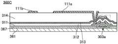
图1A是显示装置380A的截面图。FIG. 1A is a cross-sectional view of a
显示装置380A由电路板360A和LED衬底370A贴合形成。The
图1B是LED衬底370A的截面图。FIG. 1B is a cross-sectional view of
LED衬底370A包括衬底371、发光二极管302a、发光二极管302b、导电体117a、导电体117b、导电体117c、导电体117d及保护层373。The
发光二极管302a包括电极112a、半导体层113a、发光层114a、半导体层115a及电极116a。发光二极管302b包括电极112b、半导体层113b、发光层114b、半导体层115b及电极116b。The
电极112a与半导体层113a及导电体117b电连接。电极116a与半导体层115a及导电体117a电连接。电极112b与半导体层113b及导电体117d电连接。电极116b与半导体层115b及导电体117c电连接。保护层373以覆盖衬底371、电极112a、112b、半导体层113a、113b、发光层114a、114b、半导体层115a、115b、电极116a及116b的方式形成。保护层373覆盖导电体117a至117d的侧面,并包括与导电体117a至117d的顶面重叠的开口。导电体117a至117d的顶面在该开口中露出。The
发光层114a被夹在半导体层113a和半导体层115a之间。发光层114b被夹在半导体层113b和半导体层115b之间。在发光层114a、114b中,电子和空穴键合而发射光。半导体层113a、113b和半导体层115a、115b中的一个是n型半导体层,另一个是p型半导体层。包括半导体层113a、发光层114a及半导体层115a的叠层结构和包括半导体层113b、发光层114b及半导体层115b的叠层结构以各自呈现红色、黄色、绿色或蓝色等的光的方式形成。两个叠层结构优选呈现不同颜色的光。例如,可以将镓-磷化合物、镓-砷化合物、镓-铝-砷化合物、铝-镓-铟-磷化合物、镓氮化物、铟-氮化镓化合物、硒-锌化合物等用于这些叠层结构。如上所述,由于包括半导体层113a、发光层114a及半导体层115a的叠层结构以发射红色、黄色、绿色或蓝色等颜色的光的方式形成,所以不需要形成滤色片等着色膜的工序。因此,可以抑制显示装置的制造成本。此外,两个叠层结构也可以呈现相同颜色的光。此时,发光层114a、114b所发射的光也可以经过着色膜被提取到显示装置外部。The
作为衬底371,例如可以使用蓝宝石(Al2O3)衬底、碳化硅(SiC)衬底、硅(Si)衬底、氮化镓(GaN)衬底等单晶衬底。As the
图1C示出电路板360A的截面图。FIG. 1C shows a cross-sectional view of
电路板360A包括衬底361、绝缘层367、晶体管303a、晶体管303b、绝缘层314、导电层111a、导电层111b、导电层111c及导电层111d。The
晶体管303a、303b都包括栅极、栅极绝缘层311、半导体层、背栅极、源极及漏极。栅极(下侧的栅极)与半导体层隔着栅极绝缘层311重叠。背栅极(上侧的栅极)与半导体层隔着绝缘层312及绝缘层313重叠。半导体层优选包含氧化物半导体。Both the
优选对绝缘层312、绝缘层313及绝缘层314中的至少一个使用水或氢等杂质不容易扩散的材料。由此,可以有效地抑制来自外部的杂质扩散到晶体管中,从而可以提高显示装置的可靠性。绝缘层314被用作平坦化层。For at least one of the insulating
绝缘层367被用作基底膜。绝缘层367优选使用水或氢等杂质不容易扩散的材料。The insulating
如图1A所示,设置在LED衬底370A上的导电体117a与设置在电路板360A上的导电层111a连接。由此,可以使晶体管303a和发光二极管302a电连接。电极116a被用作发光二极管302a的像素电极。另外,设置在LED衬底370A上的导电体117b与设置在电路板360A上的导电层111b连接。电极112a被用作发光二极管302a的公共电极。As shown in FIG. 1A, the
同样的,设置在LED衬底370A上的导电体117c与设置在电路板360A上的导电层111c连接。由此,可以使晶体管303b与发光二极管302b电连接。电极116b被用作发光二极管302b的像素电极。另外,设置在LED衬底370A上的导电体117d与设置在电路板360A上的导电层111d连接。电极112b被用作发光二极管302b的公共电极。Similarly, the
发光二极管302a、302b所发射的光被提取到衬底361一侧。衬底361、绝缘层367、栅极绝缘层311、绝缘层312、313、314及保护层373分别可以使该光透过。The light emitted by the
注意,在本实施方式中示出发光二极管的光被提取到与衬底371相反一侧的例子,但是当衬底371可以使可见光透过的情况下,该光也可以被提取到衬底371一侧。此外,也可以在不提取光的一侧设置反射发光二极管的光的反射层或遮断该光的遮光层。Note that in this embodiment mode, an example in which the light of the light-emitting diode is extracted to the side opposite to the
例如,导电体117a至117d可以适当地使用银、碳、铜等的导电膏、金、焊料等的凸块。此外,与导电体117a至117d连接的电极112a、112b、116a、116b及导电层111a至111d都优选使用与导电体117a至117d的接触电阻低的导电材料。例如,在导电体117a至117d使用银膏时,如果与它们连接的导电材料是铝、钛、铜、银(Ag)、钯(Pd)和铜(Cu)的合金(Ag-Pd-Cu(APC))等,则接触电阻低,所以是优选的。For example, as the
注意,导电体117a至117d也可以不设置在LED衬底370A而设置在电路板360A上。Note that the
[显示装置的结构例子B][Structure Example B of Display Device]
图2A所示的显示装置380B与显示装置380A的不同之处在于包括具有柔性的衬底362及粘合层363而不包括衬底361。The
通过在玻璃衬底等的耐热性高的衬底上形成晶体管,可以形成电特性及可靠性高的晶体管。然后,通过将晶体管从该衬底剥离并转置到薄膜等具有柔性的衬底上,可以实现显示装置的薄型化及轻量化。By forming a transistor on a substrate having high heat resistance such as a glass substrate, a transistor having high electrical characteristics and reliability can be formed. Then, by peeling off the transistor from the substrate and transposing it on a flexible substrate such as a film, it is possible to reduce the thickness and weight of the display device.
参照图2B至图2D对显示装置380B的制造方法进行说明。A method of manufacturing the
如图2B所示,在衬底351上形成剥离层353,在剥离层353上形成绝缘层367。然后,在绝缘层367上形成晶体管303a、绝缘层314及导电层111a、111b。由此,可以形成电路板360B。As shown in FIG. 2B , a
接着,如图2C所示,贴合电路板360B和LED衬底370A。Next, as shown in FIG. 2C , the
然后,如图2D所示,使用剥离层353剥离衬底351。之后,通过使用粘合层363贴合露出的绝缘层367和具有柔性的衬底362,可以制造图2A示出的显示装置380B。Then, as shown in FIG. 2D , the
衬底351具有容易传送的程度的刚性,且对制造工序时的温度具有耐热性。作为可用于衬底351的材料,例如可以举出玻璃、石英、陶瓷、蓝宝石、树脂、半导体、金属或合金等。作为玻璃,例如可以举出无碱玻璃、钡硼硅酸盐玻璃、铝硼硅酸盐玻璃等。The
剥离层353可以使用有机材料或无机材料形成。The
作为可用于剥离层353的有机材料,例如可以举出聚酰亚胺树脂、丙烯酸树脂、环氧树脂、聚酰胺树脂、聚酰亚胺酰胺树脂、硅氧烷树脂、苯并环丁烯类树脂、酚醛树脂等形成。Examples of organic materials that can be used for the
作为可用于剥离层353的无机材料,可以举出包含选自钨、钼、钛、钽、铌、镍、钴、锆、锌、钌、铑、钯、锇、铱及硅中的元素的金属、包含该元素的合金或包含该元素的化合物等。包含硅的层的结晶结构可以为非晶、微晶或多晶中的任一种。Examples of inorganic materials that can be used for the
可以通过对剥离界面照射激光来剥离衬底351。作为激光,可以使用准分子激光、固体激光等。例如,也可以使用半导体泵浦固体激光(DPSS:Diode Pump Solid StateLaser)。另外,也可以施加垂直方向的拉起力量来剥离衬底351。The
注意,根据衬底351、剥离层353及绝缘层367的材料的组合,有时剥离界面会发生变化。例如,衬底351与剥离层353的界面、剥离层353中剥离层353与绝缘层367的界面等变为剥离界面。Note that depending on the combination of materials of the
[显示装置的结构例子C][Structure Example C of Display Device]
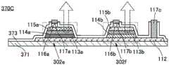
图3A是显示装置380C的截面图。FIG. 3A is a cross-sectional view of a
显示装置380C由电路板360C及LED衬底370B贴合形成。在显示装置380C中,一个晶体管与两个发光二极管电连接。如此,一个晶体管可以与多个发光二极管电连接。The
图3B是LED衬底370B的截面图。FIG. 3B is a cross-sectional view of an
LED衬底370B包括衬底371、发光二极管302c、发光二极管302d、导电体117a、导电体117b、导电体117c及保护层373。The
发光二极管302c、302d具有相同结构,并都包括电极112、半导体层113、发光层114、半导体层115及电极116。The
电极112与半导体层113及导电体117c电连接。电极116与半导体层115及导电体117a或导电体117b电连接。保护层373以覆盖衬底371、电极112、半导体层113、发光层114、半导体层115及电极116的方式形成。保护层373覆盖导电体117a至117c的侧面,并具有与导电体117a至117c的顶面重叠的开口。导电体117a至117c的顶面在该开口中露出。The
发光层114是发光层,半导体层113和半导体层115中的一个是n型半导体层,另一个是p型半导体层。以呈现相同颜色的光的方式形成发光二极管302c、302d。The
图3C是电路板360C的截面图。FIG. 3C is a cross-sectional view of
电路板360C包括衬底361、绝缘层367、晶体管303a、绝缘层314、导电层111a及导电层111b。The
如图3A所示,设置在LED衬底370B上的导电体117a、117b与设置在电路板360C上的导电层111a连接。由此,可以使晶体管303a与发光二极管302c、302d电连接。电极116被用作发光二极管302a、302b的像素电极。另外,设置在LED衬底370B上的导电体117c与设置在电路板360C上的导电层111b连接。电极112被用作发光二极管302c、302d的公共电极。在LED衬底370A(图1B)中,公共电极配置在每一个发光二极管中,但如LED衬底370B所示,公共电极(电极112)也可以横跨配置在多个发光二极管中。As shown in FIG. 3A, the
[显示装置的结构例子D、E、F][Structure Examples D, E, and F of Display Devices]
图4A是显示装置380D的截面图。FIG. 4A is a cross-sectional view of a
显示装置380D因电路阵列360D和LED衬底370C贴合而形成。如后面所述,电路阵列360D在衬底上隔着剥离层形成。然后,使将该衬底剥离而露出的电路阵列360D的面与LED衬底370C贴合。The
图4B是LED衬底370C的截面图。FIG. 4B is a cross-sectional view of an
LED衬底370C包括衬底371、发光二极管302e、发光二极管302f、导电体117a、导电体117b、导电体117c及保护层373。The
发光二极管302e包括电极112、半导体层113a、发光层114a、半导体层115a及电极116a。发光二极管302f具有电极112、半导体层113b、发光层114b、半导体层115b及电极116b。The
电极112与半导体层113a、113b及导电体117c电连接。电极116a与半导体层115a及导电体117a电连接。电极116b与半导体层115b及导电体117c电连接。保护层373以覆盖衬底371、电极112、半导体层113a、113b、发光层114a、114b、半导体层115a、115b、电极116a及116b的方式形成。保护层373覆盖导电体117a至117d的侧面,并具有与导电体117a至117d的顶面重叠的开口。导电体117a至117d的顶面在该开口中露出。The
参照图5A及图5B对电路阵列360D的制造方法进行说明。A method of manufacturing the
如图5A所示,在衬底351上形成剥离层353,并在剥离层353上形成绝缘层355。下面,对绝缘层355的一部分进行开口。然后,在绝缘层355上形成晶体管303c、303d及导电层118c。接下来,由密封层318密封晶体管303c、303d及导电层118c等。As shown in FIG. 5A , a
晶体管303c及303d都包括背栅极、栅极绝缘层311、半导体层、栅极绝缘层、栅极、绝缘层315、源极及漏极。半导体层包括沟道形成区域以及一对低电阻区域。背栅极(下侧的栅极)与沟道形成区域隔着栅极绝缘层311重叠。栅极(上侧的栅极)与沟道形成区域隔着栅极绝缘层重叠。源极及漏极通过形成在绝缘层315中的开口与低电阻区域电连接。被用作源极或漏极的导电层118a、118b通过设置在绝缘层355上的开口与剥离层353接触。此外,与导电层118a、118b使用相同材料及相同工序形成的导电层118c通过设置在绝缘层355上的开口与剥离层353接触。Both the
作为密封层318,可以使用无机绝缘材料和有机绝缘材料的一方或双方。作为密封层318的材料,可以举出能够用于粘合层等的树脂、阻挡性高的无机绝缘膜及具有柔性的树脂膜等。As the
接着,如图5B所示,利用剥离层353剥离衬底351。在图5B中,示出通过剥离而露出导电层118a、118b及118c的例子。在剥离衬底351后剥离层353有残留的情况下,通过去除剥离层353,从而使导电层118a、118b及118c露出。由此,可以形成电路阵列360D。Next, as shown in FIG. 5B , the
然后,通过贴合电路阵列360D及LED衬底370C,可以制造图4A示出的显示装置380D。Then, by laminating the
如图4A所示,使设置在LED衬底370C上的导电体117a与设置在电路阵列360D上的导电层118a连接。由此,可以电连接晶体管303e与发光二极管302e。电极116a被用作发光二极管302e的像素电极。As shown in FIG. 4A, the
同样地,使设置在LED衬底370C上的导电体117b与设置在电路阵列360D上的导电层118b连接。由此,可以电连接晶体管303f与发光二极管302f。电极116b被用作发光二极管302f的像素电极。Similarly, the
另外,使设置在LED衬底370D上的导电体117c与设置在电路阵列360D上的导电层118c连接。电极112被用作发光二极管302e、302f的公共电极。In addition, the
发光二极管302e、302f发射的光被提取到密封层318一侧。密封层318、绝缘层355、栅极绝缘层311及绝缘层315都透过该光。另外,如果将能够使可见光透过的导电材料用于导电层118a、118b,可以使发光区域比图4A所示的发光区域L1更大,所以是优选的。The light emitted by the
另外,如图6所示的显示装置380E,半导体层的低电阻区域119a、119b也可以通过形成在绝缘层355的开口与导电体117a、117b连接。当将氧化物半导体用于半导体层时,因为半导体层的低电阻区域119a、119b可以使发光二极管发射的光透过,所以可以使发光区域L2比发光区域L1更大。In addition, in the
此外,如图7所示的显示装置380F,通过使以矩阵状设置呈现相同颜色(例如白色)的光的发光二极管的LED衬底370D与具有着色层(着色层CFA、CFB)的电路阵列360F贴合,也可以制造显示装置。发光二极管302e与发光二极管302f发射相同颜色的光。发光二极管302e所发射的光经过着色层CFA被提取到显示装置380F的外部。发光二极管302f所发射的光经过与着色层CFA不同颜色的着色层CFB被提取到显示装置380F的外部。例如,通过在电路阵列360F设置红色、绿色及蓝色的着色层,可以制造能够进行全彩色显示的显示装置。In addition, in a display device 380F shown in FIG. 7 , an
注意,通过在显示装置380D的制造方法中,通过将隔着剥离层353形成在衬底351上的电路阵列360D更改为电路阵列360E或电路阵列360F,可以分别制造显示装置380E、380F。Note that by changing the
[晶体管][transistor]
接着,对可用于显示装置的晶体管进行说明。Next, transistors that can be used in a display device will be described.
对显示装置所包括的晶体管的结构没有特别的限制。例如,可以使用平面型晶体管、交错型晶体管或反交错型晶体管。此外,晶体管都可以具有顶栅结构或底栅结构。或者,也可以在沟道的上下设置有栅电极。There is no particular limitation on the structure of transistors included in the display device. For example, planar transistors, staggered transistors, or reverse staggered transistors may be used. In addition, the transistors may all have a top-gate structure or a bottom-gate structure. Alternatively, gate electrodes may be provided above and below the channel.
作为显示装置所包括的晶体管,可以使用例如将金属氧化物用于沟道形成区域的晶体管。由此,可以实现关态电流极低的晶体管。As the transistor included in the display device, for example, a transistor using a metal oxide for a channel formation region can be used. Thus, a transistor with an extremely low off-state current can be realized.
此外,作为显示装置所包括的晶体管,可以使用在沟道形成区域中含有硅的晶体管。作为该晶体管可以举出例如含有非晶硅的晶体管、含有结晶硅(典型为低温多晶硅)的晶体管、以及含有单晶硅的晶体管等。In addition, as a transistor included in the display device, a transistor containing silicon in a channel formation region can be used. Examples of such transistors include transistors containing amorphous silicon, transistors containing crystalline silicon (typically low temperature polysilicon), transistors containing single crystal silicon, and the like.
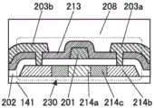
图8A及图8B示出晶体管的结构例子。各晶体管设置在绝缘层141和绝缘层208之间。绝缘层141优选被用作基底膜。绝缘层208优选被用作平坦化膜。8A and 8B show structural examples of transistors. Each transistor is provided between the insulating
图8A所示的晶体管220是在半导体层204中包括金属氧化物的底栅结构的晶体管。金属氧化物可以被用作氧化物半导体。The
作为晶体管的半导体,优选使用氧化物半导体。通过使用带隙比硅宽且载流子密度比硅小的半导体材料,可以降低晶体管的关闭状态时的电流,所以是优选的。As the semiconductor of the transistor, an oxide semiconductor is preferably used. It is preferable to use a semiconductor material having a wider band gap than silicon and a lower carrier density than silicon because the current in the off state of the transistor can be reduced.
晶体管220包括导电层201、绝缘层202、导电层203a、导电层203b及半导体层204。导电层201被用作栅极。绝缘层202被用作栅极绝缘层。半导体层204隔着绝缘层202与导电层201重叠。导电层203a及导电层203b都与半导体层204电连接。晶体管220优选被绝缘层211及绝缘层212覆盖。作为绝缘层211及绝缘层212可以使用各种无机绝缘膜。尤其是,作为绝缘层211,优选使用氧化物绝缘膜,而作为绝缘层212,优选使用氮化物绝缘膜。The
图8B所示的晶体管230是在半导体层中包含多晶硅的底栅结构的晶体管。The
晶体管230包括导电层201、绝缘层202、导电层203a、导电层203b、半导体层及绝缘层213。导电层201被用作栅极。绝缘层202被用作栅极绝缘层。半导体层包括沟道形成区域214a及一对低电阻区域214b。半导体层也可以包括LDD(Lightly Doped Drain:轻掺杂漏)区域。图8B示出在沟道形成区域214a和低电阻区域214b之间包括LDD区域214c的例子。沟道形成区域214a隔着绝缘层202与导电层201重叠。导电层203a通过设置在绝缘层202及绝缘层213的开口与一对低电阻区域214b中的一个电连接。同样地,导电层203b与一对低电阻区域214b中的另一个电连接。作为绝缘层213,可以使用各种无机绝缘膜。特别是,作为绝缘层213,优选使用氮化物绝缘膜。The
[金属氧化物][Metal oxide]
优选将被用作氧化物半导体的金属氧化物用于半导体层。以下,将说明可用于半导体层的金属氧化物。A metal oxide used as an oxide semiconductor is preferably used for the semiconductor layer. Hereinafter, metal oxides usable for the semiconductor layer will be described.
金属氧化物优选至少包含铟或锌。尤其优选包含铟及锌。另外,除此之外,还优选包含铝、镓、钇或锡等。此外,也可以包含硼、钛、铁、镍、锗、锆、钼、镧、铈、钕、铪、钽、钨或镁等中的一种或多种。The metal oxide preferably contains at least indium or zinc. In particular, it is preferable to contain indium and zinc. In addition, aluminum, gallium, yttrium, tin, or the like is preferably contained in addition to these. In addition, one or more of boron, titanium, iron, nickel, germanium, zirconium, molybdenum, lanthanum, cerium, neodymium, hafnium, tantalum, tungsten, or magnesium may also be included.
在此,考虑金属氧化物是包含铟、元素M及锌的In-M-Zn氧化物的情况。注意,元素M为铝、镓、钇或锡等。作为其他可用作元素M的元素,有硼、钛、铁、镍、锗、锆、钼、镧、铈、钕、铪、钽、钨、镁等。注意,作为元素M有时也可以组合多个上述元素。Here, consider a case where the metal oxide is an In-M-Zn oxide containing indium, element M, and zinc. Note that the element M is aluminum, gallium, yttrium, or tin, or the like. As other elements usable as the element M, there are boron, titanium, iron, nickel, germanium, zirconium, molybdenum, lanthanum, cerium, neodymium, hafnium, tantalum, tungsten, magnesium, and the like. Note that, as the element M, a plurality of the above-mentioned elements may sometimes be combined.
另外,在本说明书等中,有时将包含氮的金属氧化物称为金属氧化物(metaloxide)。此外,也可以将包含氮的金属氧化物称为金属氧氮化物(metal oxynitride)。例如,也可以将锌氧氮化物(ZnON)等含有氮的金属氧化物用于半导体层。In addition, in this specification etc., the metal oxide containing nitrogen may be called a metal oxide (metal oxide). In addition, metal oxides containing nitrogen may also be called metal oxynitrides. For example, a nitrogen-containing metal oxide such as zinc oxynitride (ZnON) may be used for the semiconductor layer.
在本说明书等中,有时记载CAAC(c-axis aligned crystal)或CAC(Cloud-Aligned Composite)。注意,CAAC是指结晶结构的一个例子,CAC是指功能或材料构成的一个例子。In this specification and the like, CAAC (c-axis aligned crystal) or CAC (Cloud-Aligned Composite) may be described. Note that CAAC refers to an example of crystal structure, and CAC refers to an example of function or material composition.
例如,作为半导体层,可以使用CAC(Cloud-Aligned Composite)-OS。For example, a CAC (Cloud-Aligned Composite)-OS can be used as the semiconductor layer.
CAC-OS或CAC-metal oxide在材料的一部分中具有导电性的功能,在材料的另一部分中具有绝缘性的功能,作为材料的整体具有半导体的功能。此外,在将CAC-OS或CAC-metal oxide用于晶体管的发光层的情况下,导电性的功能是使被用作载流子的电子(或空穴)流过的功能,绝缘性的功能是不使被用作载流子的电子流过的功能。通过导电性的功能和绝缘性的功能的互补作用,可以使CAC-OS或CAC-metal oxide具有开关功能(控制开启/关闭的功能)。通过在CAC-OS或CAC-metal oxide中使各功能分离,可以最大限度地提高各功能。CAC-OS or CAC-metal oxide has a conductive function in a part of the material, an insulating function in another part of the material, and a semiconductor function as a whole of the material. In addition, when CAC-OS or CAC-metal oxide is used for the light-emitting layer of a transistor, the function of conductivity is the function of allowing electrons (or holes) used as carriers to flow, and the function of insulation It is a function not to flow electrons used as carriers. CAC-OS or CAC-metal oxide can have a switching function (function to control ON/OFF) through the complementarity of the conductive function and the insulating function. Each function can be maximized by separating each function in CAC-OS or CAC-metal oxide.
此外,CAC-OS或CAC-metal oxide包括导电性区域及绝缘性区域。导电性区域具有上述导电性的功能,绝缘性区域具有上述绝缘性的功能。此外,在材料中,导电性区域和绝缘性区域有时以纳米粒子级分离。另外,导电性区域和绝缘性区域有时在材料中不均匀地分布。此外,有时观察到其边缘模糊而以云状连接的导电性区域。In addition, CAC-OS or CAC-metal oxide includes a conductive region and an insulating region. The conductive region has the aforementioned conductive function, and the insulating region has the aforementioned insulating function. In addition, in materials, conductive regions and insulating regions are sometimes separated at the nanoparticle level. In addition, conductive regions and insulating regions are sometimes unevenly distributed in the material. In addition, conductive regions whose edges are blurred and connected in a cloud shape are sometimes observed.
此外,在CAC-OS或CAC-metal oxide中,导电性区域和绝缘性区域有时以0.5nm以上且10nm以下,优选为0.5nm以上且3nm以下的尺寸分散在材料中。In addition, in CAC-OS or CAC-metal oxide, conductive domains and insulating domains may be dispersed in the material with a size of 0.5 nm to 10 nm, preferably 0.5 nm to 3 nm.
此外,CAC-OS或CAC-metal oxide由具有不同带隙的成分构成。例如,CAC-OS或CAC-metal oxide由具有起因于绝缘性区域的宽隙的成分及具有起因于导电性区域的窄隙的成分构成。在该结构中,当使载流子流过时,载流子主要在具有窄隙的成分中流过。此外,具有窄隙的成分与具有宽隙的成分互补作用,与具有窄隙的成分联动地在具有宽隙的成分中载流子流过。因此,在将上述CAC-OS或CAC-metal oxide用于晶体管的沟道形成区域时,在晶体管的导通状态中可以得到高电流驱动力,即大通态电流及高场效应迁移率。In addition, CAC-OS or CAC-metal oxide is composed of components with different band gaps. For example, CAC-OS or CAC-metal oxide is composed of a component having wide gaps originating from an insulating region and a component having narrow gaps originating in a conductive region. In this structure, when carriers are made to flow, the carriers mainly flow through the composition having narrow gaps. In addition, the component having the narrow gap acts complementary to the component having the wide gap, and carriers flow through the component having the wide gap in conjunction with the component having the narrow gap. Therefore, when the above-mentioned CAC-OS or CAC-metal oxide is used in the channel formation region of the transistor, a high current driving force, that is, a large on-state current and high field-effect mobility can be obtained in the on state of the transistor.
就是说,也可以将CAC-OS或CAC-metal oxide称为基质复合材料(matrixcomposite)或金属基质复合材料(metal matrix composite)。That is, CAC-OS or CAC-metal oxide may also be called a matrix composite material (matrix composite) or a metal matrix composite material (metal matrix composite).
氧化物半导体(金属氧化物)被分为单晶氧化物半导体和非单晶氧化物半导体。作为非单晶氧化物半导体例如有CAAC-OS(c-axis aligned crystalline oxidesemiconductor)、多晶氧化物半导体、nc-OS(nanocrystalline oxide semiconductor)、a-like OS(amorphous-like oxide semiconductor)及非晶氧化物半导体等。Oxide semiconductors (metal oxides) are classified into single crystal oxide semiconductors and non-single crystal oxide semiconductors. Examples of non-single crystal oxide semiconductors include CAAC-OS (c-axis aligned crystalline oxide semiconductor), polycrystalline oxide semiconductor, nc-OS (nanocrystalline oxide semiconductor), a-like OS (amorphous-like oxide semiconductor), and amorphous oxide semiconductors, etc.
CAAC-OS具有c轴取向性,其多个纳米晶在a-b面方向上连结而结晶结构具有畸变。畸变是指在多个纳米晶连结的区域中晶格排列一致的区域与其他晶格排列一致的区域之间的晶格排列的方向变化的部分。CAAC-OS has c-axis orientation, and its multiple nanocrystals are connected in the a-b plane direction, and the crystal structure has distortion. Distortion refers to a portion in which the direction of lattice alignment changes between a region where the lattice alignment is consistent and other regions where the lattice alignment is consistent among regions where a plurality of nanocrystals are connected.
纳米晶基本上为六角形,但是不局限于正六角形,有时为非正六角形。此外,在畸变中有时具有五角形或七角形等晶格排列。另外,在CAAC-OS中,即使在畸变附近也难以观察到明确的晶界(grain boundary)。即,可知由于晶格排列畸变,可抑制晶界的形成。这是由于CAAC-OS因为a-b面方向上的氧原子排列的低密度或因金属元素被取代而使原子间的键合距离产生变化等而能够包容畸变。Nanocrystals are basically hexagonal, but not limited to regular hexagonal, and sometimes non-regular hexagonal. In addition, there are sometimes lattice arrangements such as pentagons or heptagons in distortion. In addition, in CAAC-OS, it is difficult to observe a clear grain boundary (grain boundary) even in the vicinity of distortion. That is, it can be seen that the formation of grain boundaries can be suppressed due to the distortion of the lattice arrangement. This is because CAAC-OS can tolerate distortion due to the low density of oxygen atom arrangement in the a-b plane direction or the change in the bonding distance between atoms due to the substitution of metal elements.
CAAC-OS有具有层状结晶结构(也称为层状结构)的倾向,在该层状结晶结构中层叠有包含铟及氧的层(下面称为In层)和包含元素M、锌及氧的层(下面称为(M,Zn)层)。另外,铟和元素M彼此可以取代,在用铟取代(M,Zn)层中的元素M的情况下,也可以将该层表示为(In,M,Zn)层。另外,在用元素M取代In层中的铟的情况下,也可以将该层表示为(In,M)层。CAAC-OS tends to have a layered crystal structure (also called layered structure) in which layers containing indium and oxygen (hereinafter referred to as In layers) and layers containing elements M, zinc, and oxygen are laminated. layer (hereinafter referred to as (M, Zn) layer). In addition, indium and the element M may be substituted for each other, and when the element M in the (M, Zn) layer is substituted with indium, the layer may also be represented as an (In, M, Zn) layer. In addition, when indium in the In layer is replaced with an element M, this layer can also be expressed as an (In, M) layer.
CAAC-OS是结晶性高的金属氧化物。另一方面,在CAAC-OS中不容易观察明确的晶界,因此不容易发生起因于晶界的电子迁移率的下降。此外,金属氧化物的结晶性有时因杂质的进入或缺陷的生成等而降低,因此可以说CAAC-OS是杂质或缺陷(氧空位(也称为VO(oxygen vacancy))等)少的金属氧化物。因此,包含CAAC-OS的金属氧化物的物理性质稳定。因此,具有CAAC-OS的金属氧化物具有耐热性及高可靠性。CAAC-OS is a highly crystalline metal oxide. On the other hand, in CAAC-OS, it is not easy to observe clear grain boundaries, and therefore, the decrease in electron mobility due to grain boundaries does not easily occur. In addition, the crystallinity of metal oxides may decrease due to the entry of impurities or the generation of defects, so it can be said that CAAC-OS is a metal with few impurities or defects (oxygen vacancies (also calledVO (oxygen vacancy), etc.) oxide. Therefore, the physical properties of the metal oxide including CAAC-OS are stable. Therefore, metal oxides having CAAC-OS have heat resistance and high reliability.
在nc-OS中,微小的区域(例如1nm以上且10nm以下的区域,特别是1nm以上且3nm以下的区域)中的原子排列具有周期性。另外,nc-OS在不同的纳米晶之间观察不到结晶取向的规律性。因此,在膜整体中观察不到取向性。所以,有时nc-OS在某些分析方法中与a-likeOS或非晶氧化物半导体没有差别。In nc-OS, the arrangement of atoms in a minute region (for example, a region of 1 nm to 10 nm, particularly a region of 1 nm to 3 nm) has periodicity. In addition, nc-OS does not observe the regularity of crystallographic orientation among different nanocrystals. Therefore, no orientation was observed in the entire film. So, sometimes nc-OS does not differ from a-likeOS or amorphous oxide semiconductor in some analytical methods.
另外,在包含铟、镓和锌的金属氧化物的一种的铟-镓-锌氧化物(以下,IGZO)有时在由上述纳米晶构成时具有稳定的结构。尤其是,IGZO有在大气中不容易进行晶体生长的倾向,所以有时与在IGZO由大结晶(在此,几mm的结晶或者几cm的结晶)形成时相比在IGZO由小结晶(例如,上述纳米结晶)形成时在结构上稳定。Also, indium-gallium-zinc oxide (hereinafter, IGZO), one of metal oxides including indium, gallium, and zinc, sometimes has a stable structure when it is composed of the aforementioned nanocrystals. In particular, IGZO tends to be difficult to grow crystals in the atmosphere, so IGZO may be formed from small crystals (for example, The aforementioned nanocrystals) are structurally stable when formed.
a-like OS是具有介于nc-OS与非晶氧化物半导体之间的结构的金属氧化物。a-like OS包含空洞或低密度区域。也就是说,a-like OS的结晶性比nc-OS及CAAC-OS的结晶性低。a-like OS is a metal oxide having a structure between nc-OS and amorphous oxide semiconductor. The a-like OS contains voids or areas of low density. That is, the crystallinity of a-like OS is lower than that of nc-OS and CAAC-OS.
氧化物半导体(金属氧化物)具有各种结构及各种特性。本发明的一个方式的氧化物半导体也可以包括非晶氧化物半导体、多晶氧化物半导体、a-like OS、nc-OS、CAAC-OS中的两种以上。Oxide semiconductors (metal oxides) have various structures and various characteristics. The oxide semiconductor in one embodiment of the present invention may include two or more of amorphous oxide semiconductor, polycrystalline oxide semiconductor, a-like OS, nc-OS, and CAAC-OS.
用作半导体层的金属氧化物膜可以使用惰性气体和氧气体中的任一个或两个形成。注意,对形成金属氧化物膜时的氧流量比(氧分压)没有特别的限制。但是,在要获得场效应迁移率高的晶体管的情况下,形成金属氧化物膜时的氧流量比(氧分压)优选为0%以上且30%以下,更优选为5%以上且30%以下,进一步优选为7%以上且15%以下。A metal oxide film serving as a semiconductor layer can be formed using either or both of an inert gas and an oxygen gas. Note that there is no particular limitation on the oxygen flow ratio (oxygen partial pressure) at the time of forming the metal oxide film. However, in order to obtain a transistor with high field-effect mobility, the oxygen flow ratio (oxygen partial pressure) when forming the metal oxide film is preferably 0% or more and 30% or less, more preferably 5% or more and 30% or less. Below, more preferably 7% or more and 15% or less.
金属氧化物的能隙优选为2eV以上,更优选为2.5eV以上,进一步优选为3eV以上。如此,通过使用能隙较宽的金属氧化物,可以降低晶体管的关态电流。The energy gap of the metal oxide is preferably 2 eV or more, more preferably 2.5 eV or more, and still more preferably 3 eV or more. Thus, by using a metal oxide with a wide energy gap, the off-state current of the transistor can be reduced.
金属氧化物膜可以通过溅射法形成。除此之外,还可以利用PLD法、PECVD法、热CVD法、ALD法、真空蒸镀法等。The metal oxide film can be formed by a sputtering method. In addition, a PLD method, a PECVD method, a thermal CVD method, an ALD method, a vacuum vapor deposition method, or the like can be used.
作为可用于构成显示装置的各种导电层的材料,可以举出铝、钛、铬、镍、铜、钇、锆、钼、银、钽或钨等金属或者以上述金属为主要成分的合金等。另外,可以以单层或叠层结构使用包含这些材料的膜。例如,可以举出包含硅的铝膜的单层结构、在钛膜上层叠铝膜的两层结构、在钨膜上层叠铝膜的两层结构、在铜-镁-铝合金膜上层叠铜膜的两层结构、在钛膜上层叠铜膜的两层结构、在钨膜上层叠铜膜的两层结构、依次层叠钛膜或氮化钛膜、铝膜或铜膜以及钛膜或氮化钛膜的三层结构、以及依次层叠钼膜或氮化钼膜、铝膜或铜膜以及钼膜或氮化钼膜的三层结构等。另外,可以使用氧化铟、氧化锡或氧化锌等氧化物。另外,通过使用包含锰的铜,可以提高蚀刻时的形状的控制性,所以是优选的。Examples of materials that can be used for various conductive layers constituting a display device include metals such as aluminum, titanium, chromium, nickel, copper, yttrium, zirconium, molybdenum, silver, tantalum, or tungsten, or alloys containing the above metals as main components. . In addition, films containing these materials may be used in a single-layer or laminated structure. Examples include a single-layer structure of an aluminum film containing silicon, a two-layer structure of laminating an aluminum film on a titanium film, a two-layer structure of laminating an aluminum film on a tungsten film, and laminating a copper film on a copper-magnesium-aluminum alloy film. Two-layer structure of the film, two-layer structure of stacking copper film on titanium film, two-layer structure of stacking copper film on tungsten film, sequentially stacking titanium film or titanium nitride film, aluminum film or copper film, and titanium film or nitrogen film The three-layer structure of titanium oxide film, and the three-layer structure of sequentially stacking molybdenum film or molybdenum nitride film, aluminum film or copper film, molybdenum film or molybdenum nitride film, etc. In addition, oxides such as indium oxide, tin oxide, or zinc oxide can be used. In addition, the use of copper containing manganese is preferable since the controllability of the shape during etching can be improved.
作为可用于构成显示装置的各绝缘层的绝缘材料,例如可以举出如丙烯酸、聚酰亚胺、环氧及硅酮等树脂、如氧化硅、氧氮化硅、氮氧化硅、氮化硅或氧化铝等无机绝缘材料。As the insulating material that can be used for each insulating layer of the display device, resins such as acrylic, polyimide, epoxy and silicone, such as silicon oxide, silicon oxynitride, silicon nitride oxide, silicon nitride, etc., can be mentioned, for example. Or inorganic insulating materials such as alumina.
如上所述,在本实施方式的显示装置中,可以一次贴合多个发光二极管和多个晶体管,因此可以实现显示装置的制造成本的缩减及成品率的提高。此外,通过组合微型LED和使用金属氧化物的晶体管,可以实现功耗得到减少的显示装置。As described above, in the display device of the present embodiment, a plurality of light emitting diodes and a plurality of transistors can be bonded together at one time, so that reduction in manufacturing cost of the display device and improvement in yield can be achieved. Furthermore, by combining micro LEDs and transistors using metal oxides, it is possible to realize a display device in which power consumption is reduced.
本实施方式可以与其他实施方式适当地组合。此外,在本说明书中,在一个实施方式中示出多个结构例子的情况下,可以适当地组合该结构例子。This embodiment mode can be appropriately combined with other embodiment modes. In addition, in this specification, when a plurality of structural examples are shown in one embodiment, the structural examples can be combined appropriately.
(实施方式2)(Embodiment 2)
在本实施方式中,参照图9至图11对本发明的一个方式的电子设备进行说明。In this embodiment, an electronic device according to one embodiment of the present invention will be described with reference to FIGS. 9 to 11 .
本实施方式的电子设备在显示部中包括本发明的一个方式的显示装置。本发明的一个方式的显示装置的显示质量高且功耗低。另外,本发明的一个方式的显示装置容易实现高分辨率及大型化。因此,可以用于各种电子设备的显示部。An electronic device according to this embodiment includes a display device according to one embodiment of the present invention in a display unit. A display device according to one aspect of the present invention has high display quality and low power consumption. In addition, the display device according to one aspect of the present invention can easily achieve high resolution and increase in size. Therefore, it can be used for display portions of various electronic devices.
在本实施方式的电子设备的显示部上例如可以显示具有全高清、4K2K、8K4K、16K8K或更高的分辨率的影像。Videos having resolutions of, for example, full high-definition, 4K2K, 8K4K, 16K8K or higher can be displayed on the display unit of the electronic device according to this embodiment.
作为电子设备,例如除了电视装置、台式或笔记本型个人计算机、用于计算机等的显示器、数字标牌及弹珠机等大型游戏机等具有比较大的屏幕的电子设备之外,还可以举出数码相机、数码摄像机、数码相框、移动电话机、便携式游戏机、便携式信息终端、声音再现装置等。Examples of electronic equipment include electronic equipment with relatively large screens such as television sets, desktop or notebook personal computers, monitors for computers, digital signage, and large game machines such as pachinko machines. Cameras, digital video cameras, digital photo frames, mobile phones, portable game machines, portable information terminals, audio reproduction devices, etc.
可以将本实施方式的电子设备沿着房屋或高楼的内壁或外壁、汽车等的内部装饰或外部装饰的曲面组装。The electronic device of this embodiment can be assembled along the inner or outer walls of houses or high-rise buildings, or the curved surfaces of the interior or exterior of automobiles or the like.
本实施方式的电子设备也可以包括天线。通过由天线接收信号,可以在显示部上显示影像或信息等。此外,在电子设备包括天线及二次电池时,可以将天线用于非接触电力传送。The electronic device of this embodiment may also include an antenna. By receiving signals from the antenna, images, information, etc. can be displayed on the display unit. Also, when the electronic device includes an antenna and a secondary battery, the antenna can be used for non-contact power transmission.
本实施方式的电子设备也可以包括传感器(该传感器具有测量如下因素的功能:力、位移、位置、速度、加速度、角速度、转速、距离、光、液、磁、温度、化学物质、声音、时间、硬度、电场、电流、电压、电力、辐射线、流量、湿度、倾斜度、振动、气味或红外线)。The electronic device of this embodiment may also include a sensor (the sensor has the function of measuring the following factors: force, displacement, position, velocity, acceleration, angular velocity, rotational speed, distance, light, liquid, magnetism, temperature, chemical substance, sound, time , hardness, electric field, current, voltage, electricity, radiation, flow, humidity, inclination, vibration, odor or infrared).
本实施方式的电子设备可以具有各种功能。例如,可以具有如下功能:将各种信息(静态图像、动态图像、文字图像等)显示在显示部上的功能;触摸面板的功能;显示日历、日期或时间等的功能;执行各种软件(程序)的功能;进行无线通信的功能;读出储存在存储介质中的程序或信息的功能;等。The electronic device of this embodiment can have various functions. For example, the following functions may be provided: the function of displaying various information (still images, moving images, text images, etc.) on the display part; the function of the touch panel; program) function; the function of performing wireless communication; the function of reading out the program or information stored in the storage medium; etc.
图9A示出电视装置的一个例子。电视装置7100的显示部7000被组装在外壳7101中。在此示出利用支架7103支撑外壳7101的结构。FIG. 9A shows an example of a television set. The
可以将本发明的一个方式的显示装置用于显示部7000。A display device according to one embodiment of the present invention can be used for the
可以通过利用外壳7101所具备的操作开关或另外提供的遥控操作机7111进行图9A所示的电视装置7100的操作。此外,显示部7000也可以具备触摸传感器,通过用手指触摸显示部7000可以进行电视装置7100的操作。遥控操作机7111也可以具备显示从该遥控操作机7111输出的信息的显示部。可以通过利用遥控操作机7111所具备的操作键或触摸面板进行频道及音量的操作,并可以对显示在显示部7000上的影像进行操作。Operation of the
注意,电视装置7100采用具备接收机及调制解调器等的结构。可以通过接收机接收一般的电视广播。此外,也可以通过调制解调器连接到有线或无线方式的通信网络,从而进行单向(从发送者到接收者)或双向(发送者和接收者之间或接收者之间等)的信息通信。Note that
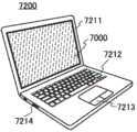
图9B示出笔记型个人计算机的一个例子。笔记型个人计算机7200包括外壳7211、键盘7212、指向装置7213、外部连接端口7214等。在外壳7211中组装有显示部7000。Fig. 9B shows an example of a notebook personal computer. A notebook
可以将本发明的一个方式的显示装置用于显示部7000。A display device according to one embodiment of the present invention can be used for the
图9C和图9D示出数字标牌(Digital Signage)的一个例子。9C and 9D show an example of digital signage (Digital Signage).
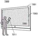
图9C所示的数字标牌7300包括外壳7301、显示部7000及扬声器7303等。此外,还可以包括LED灯、操作键(包括电源开关或操作开关)、连接端子、各种传感器以及麦克风等。The
图9D示出设置在圆柱状柱子7401上的数字标牌7400。数字标牌7400包括沿着柱子7401的曲面设置的显示部7000。FIG. 9D shows
本发明的一个方式的显示装置可以应用于图9C和图9D所示的显示部7000。The display device of one embodiment of the present invention can be applied to the
显示部7000越大,一次能够提供的信息量越多。另外,显示部7000越大,越容易吸引人的注意,例如可以提高广告宣传效果。The larger the
通过将触摸面板用于显示部7000,不仅可以在显示部7000上显示静态图像或动态图像,使用者还可以进行直觉性的操作,所以是优选的。另外,在用于提供路线信息或交通信息等信息的用途时,可以通过直觉性的操作提高易用性。By using the touch panel for the
如图9C和图9D所示,数字标牌7300或数字标牌7400优选通过无线通信可以与使用者所携带的智能手机等信息终端设备7311或信息终端设备7411联动。例如,显示在显示部7000上的广告的信息可以显示在信息终端设备7311或信息终端设备7411的屏幕。另外,通过操作信息终端设备7311或信息终端设备7411,可以切换显示部7000的显示。As shown in FIG. 9C and FIG. 9D ,
此外,可以在数字标牌7300或数字标牌7400上以信息终端设备7311或信息终端设备7411为操作单元(控制器)执行游戏。由此,不特定多个使用者可以同时参加游戏,享受游戏的乐趣。In addition, a game can be executed on the
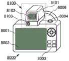
图10A是安装有取景器8100的照相机8000的外观图。FIG. 10A is an external view of a
照相机8000包括外壳8001、显示部8002、操作按钮8003、快门按钮8004等。此外,照相机8000安装有可装卸的镜头8006。注意,在照相机8000中,镜头8006和外壳也可以被形成为一体。A
通过按下快门按钮8004或者触摸用作触摸面板的显示部8002,照相机8000可以进行成像。The
外壳8001包括具有电极的嵌入器,除了可以与取景器8100连接以外,还可以与闪光灯装置等连接。The
取景器8100包括外壳8101、显示部8102以及按钮8103等。The
外壳8101通过嵌合到照相机8000的嵌入器的嵌入器安装到照相机8000。取景器8100可以将从照相机8000接收的图像等显示到显示部8102上。The
按钮8103被用作电源按钮等。The
本发明的一个方式的显示装置可以用于照相机8000的显示部8002及取景器8100的显示部8102。此外,也可以在照相机8000中内置有取景器。A display device according to one embodiment of the present invention can be used for the
图10B是头戴显示器8200的外观图。FIG. 10B is an external view of the head-mounted
头戴显示器8200包括安装部8201、透镜8202、主体8203、显示部8204以及电缆8205等。此外,在安装部8201中内置有电池8206。The head-mounted
通过电缆8205,将电力从电池8206供应到主体8203。主体8203具备无线接收器等,能够将所接收的图像信息等显示到显示部8204上。此外,主体8203具有照相机,由此可以利用使用者的眼球及眼睑的动作作为输入方法。Power is supplied from the
此外,也可以对安装部8201的被使用者接触的位置设置多个电极,以检测出根据使用者的眼球的动作而流过电极的电流,由此实现识别使用者的视线的功能。此外,还可以具有根据流过该电极的电流监视使用者的脉搏的功能。安装部8201可以具有温度传感器、压力传感器、加速度传感器等各种传感器,也可以具有将使用者的生物信息显示在显示部8204上的功能或与使用者的头部的动作同步地使显示在显示部8204上的图像变化的功能。In addition, a plurality of electrodes may be provided on the position of the mounting
可以将本发明的一个方式的显示装置用于显示部8204。A display device according to one embodiment of the present invention can be used for the
图10C、图10D及图10E是头戴显示器8300的外观图。头戴显示器8300包括外壳8301、显示部8302、带状固定工具8304以及一对透镜8305。FIG. 10C , FIG. 10D and FIG. 10E are external views of the head-mounted
使用者可以通过透镜8305看到显示部8302上的显示。优选弯曲配置显示部8302,这是因为使用者可以感受高真实感。此外,通过透镜8305分别看到显示在显示部8302的不同区域上的不同图像,可以进行利用视差的三维显示等。此外,本发明的一个方式不局限于设置有一个显示部8302的结构,也可以以对使用者的一个眼睛配置一个显示部的方式设置两个显示部8302。The user can see the display on the
可以将本发明的一个方式的显示装置用于显示部8302。因为本发明的一个方式的显示装置具有极高的分辨率,所以即使如图10E那样地使用透镜8305放大显示并观看,使用者也难以观看到像素。就是说,可以利用显示部8302使使用者观看到现实感更高的影像。A display device according to one embodiment of the present invention can be used for the
图11A至图11F所示的电子设备包括外壳9000、显示部9001、扬声器9003、操作键9005(包括电源开关或操作开关)、连接端子9006、传感器9007(该传感器具有测量如下因素的功能:力、位移、位置、速度、加速度、角速度、转速、距离、光、液、磁、温度、化学物质、声音、时间、硬度、电场、电流、电压、电力、辐射线、流量、湿度、倾斜度、振动、气味或红外线)、麦克风9008等。The electronic equipment shown in FIGS. 11A to 11F includes a
图11A至图11F所示的电子设备具有各种功能。例如,可以具有如下功能:将各种信息(静态图像、动态图像、文字图像等)显示在显示部上的功能;触摸面板的功能;显示日历、日期或时间等的功能;通过利用各种软件(程序)控制处理的功能;进行无线通信的功能;读出储存在存储介质中的程序或信息来处理的功能;等。注意,电子设备的功能不局限于上述功能,而可以具有各种功能。电子设备可以包括多个显示部。此外,也可以在该电子设备中设置照相机等而使其具有如下功能:拍摄静态图像或动态图像来将所拍摄的图像储存在存储介质(外部存储介质或内置于照相机的存储介质)中的功能;将所拍摄的图像显示在显示部上的功能;等。The electronic devices shown in FIGS. 11A to 11F have various functions. For example, it may have the following functions: the function of displaying various information (still images, moving images, text images, etc.) on the display part; the function of the touch panel; the function of displaying the calendar, date or time; (Program) A function of controlling processing; a function of performing wireless communication; a function of reading out a program or information stored in a storage medium to process; etc. Note that the functions of the electronic device are not limited to the above functions, but may have various functions. An electronic device may include a plurality of displays. In addition, a camera or the like may be installed in the electronic device to have a function of capturing still images or moving images and storing the captured images in a storage medium (external storage medium or storage medium built into the camera) ; a function of displaying a captured image on a display unit; and the like.
下面,详细地说明图11A至图11F所示的电子设备。Next, the electronic equipment shown in FIGS. 11A to 11F will be described in detail.
图11A是示出便携式信息终端9101的立体图。便携式信息终端9101例如可以用作智能手机。便携式信息终端9101也可以设置有扬声器9003、连接端子9006、传感器9007等。此外,便携式信息终端9101可以将文字或图像信息显示在其多个面上。图11A示出显示三个图标9050的例子。此外,也可以将由虚线矩形表示的信息9051显示在显示部9001的另一个面上。作为信息9051的一个例子,可以举出提示收到电子邮件、SNS或电话等的信息;电子邮件或SNS等的标题或发送者姓名;日期;时间;电池余量;以及天线接收信号强度等。或者,可以在显示有信息9051的位置上显示图标9050等。FIG. 11A is a perspective view showing a
图11B是示出便携式信息终端9102的立体图。便携式信息终端9102具有将信息显示在显示部9001的三个以上的面上的功能。在此,示出信息9052、信息9053、信息9054分别显示于不同的面上的例子。例如,使用者也可以在将便携式信息终端9102放在上衣口袋里的状态下确认显示在能够从便携式信息终端9102的上方观察到的位置上的信息9053。使用者可以确认到该显示而无需从口袋里拿出便携式信息终端9102,由此能够判断例如是否接电话。FIG. 11B is a perspective view showing the
图11C是示出手表型便携式信息终端9200的立体图。便携式信息终端9200例如可以用作智能手表。此外,显示部9001的显示面被弯曲,能够在所弯曲的显示面上进行显示。例如,通过与可进行无线通信的耳麦相互通信,便携式信息终端9200可以进行免提通话。此外,便携式信息终端9200包括连接端子9006,可以与其他信息终端进行信息的交换或者进行充电。此外,充电工作也可以利用无线供电进行。FIG. 11C is a perspective view showing a wristwatch-type
图11D、图11E及图11F是示出能够折叠的便携式信息终端9201的立体图。此外,图11D是便携式信息终端9201为展开状态的立体图,图11E是便携式信息终端9201为折叠状态的立体图,并且图11F是便携式信息终端9201为从图11D和图11F中的一个状态变为另一个状态的中途的状态的立体图。便携式信息终端9201在折叠状态下可携带性好,在展开状态下因为具有无缝拼接的较大的显示区域而其显示的一览性优异。便携式信息终端9201所包括的显示部9001由铰链9055所连接的三个外壳9000来支撑。例如,可以以0.1mm以上且150mm以下的曲率半径使显示部9001弯曲。11D , 11E , and 11F are perspective views showing a foldable
本实施方式可以与其他实施方式及实施例适当地组合。This embodiment mode can be appropriately combined with other embodiment modes and examples.
[符号说明][Symbol Description]
111a:导电层、111b:导电层、111c:导电层、111d:导电层、112:电极、112a:电极、112b:电极、113:半导体层、113a:半导体层、113b:半导体层、114:发光层、114a:发光层、114b:发光层、115:半导体层、115a:半导体层、115b:半导体层、116:电极、116a:电极、116b:电极、117a:导电体、117b:导电体、117c:导电体、117d:导电体、118a:导电层、118b:导电层、118c:导电层、119a:低电阻区域、119b:低电阻区域、141:绝缘层、201:导电层、202:绝缘层、203a:导电层、203b:导电层、204:半导体层、208:绝缘层、211:绝缘层、212:绝缘层、213:绝缘层、214a:沟道形成区域、214b:低电阻区域、214c:LDD区域、220:晶体管、230:晶体管、302a:发光二极管、302b:发光二极管、302c:发光二极管、302d:发光二极管、302e:发光二极管、302f:发光二极管、303a:晶体管、303b:晶体管、303c:晶体管、303d:晶体管、303e:晶体管、303f:晶体管、311:栅极绝缘层、312:绝缘层、313:绝缘层、314:绝缘层、315:绝缘层、318:密封层、351:衬底、353:剥离层、355:绝缘层、360A:电路板、360B:电路板、360C:电路板、360D:电路阵列、360E:电路阵列、360F:电路阵列、361:衬底、362:衬底、363:粘合层、367:绝缘层、370A:LED衬底、370B:LED衬底、370C:LED衬底、370D:LED衬底、371:衬底、373:保护层、380A:显示装置、380B:显示装置、380C:显示装置、380D:显示装置、380E:显示装置、380F:显示装置、7000:显示部、7100:电视装置、7101:外壳、7103:支架、7111:遥控操作机、7200:笔记型个人计算机、7211:外壳、7212:键盘、7213:指向装置、7214:外部连接端口、7300:数字标牌、7301:外壳、7303:扬声器、7311:信息终端设备、7400:数字标牌、7401:柱子、7411:信息终端设备、8000:照相机、8001:外壳、8002:显示部、8003:操作按钮、8004:快门按钮、8006:镜头、8100:取景器、8101:外壳、8102:显示部、8103:按钮、8200:头戴显示器、8201:安装部、8202:透镜、8203:主体、8204:显示部、8205:电缆、8206:电池、8300:头戴显示器、8301:外壳、8302:显示部、8304:固定工具、8305:透镜、9000:外壳、9001:显示部、9003:扬声器、9005:操作键、9006:连接端子、9007:传感器、9008:麦克风、9050:图标、9051:信息、9052:信息、9053:信息、9054:信息、9055:铰链、9101:便携式信息终端、9102:便携式信息终端、9200:便携式信息终端、9201:便携式信息终端111a: conductive layer, 111b: conductive layer, 111c: conductive layer, 111d: conductive layer, 112: electrode, 112a: electrode, 112b: electrode, 113: semiconductor layer, 113a: semiconductor layer, 113b: semiconductor layer, 114: light emitting layer, 114a: light emitting layer, 114b: light emitting layer, 115: semiconductor layer, 115a: semiconductor layer, 115b: semiconductor layer, 116: electrode, 116a: electrode, 116b: electrode, 117a: conductor, 117b: conductor, 117c : Conductor, 117d: Conductor, 118a: Conductive layer, 118b: Conductive layer, 118c: Conductive layer, 119a: Low resistance area, 119b: Low resistance area, 141: Insulating layer, 201: Conductive layer, 202: Insulating layer , 203a: conductive layer, 203b: conductive layer, 204: semiconductor layer, 208: insulating layer, 211: insulating layer, 212: insulating layer, 213: insulating layer, 214a: channel formation region, 214b: low resistance region, 214c : LDD area, 220: transistor, 230: transistor, 302a: light emitting diode, 302b: light emitting diode, 302c: light emitting diode, 302d: light emitting diode, 302e: light emitting diode, 302f: light emitting diode, 303a: transistor, 303b: transistor, 303c: transistor, 303d: transistor, 303e: transistor, 303f: transistor, 311: gate insulating layer, 312: insulating layer, 313: insulating layer, 314: insulating layer, 315: insulating layer, 318: sealing layer, 351: Substrate, 353: peeling layer, 355: insulating layer, 360A: circuit board, 360B: circuit board, 360C: circuit board, 360D: circuit array, 360E: circuit array, 360F: circuit array, 361: substrate, 362: Substrate, 363: adhesive layer, 367: insulating layer, 370A: LED substrate, 370B: LED substrate, 370C: LED substrate, 370D: LED substrate, 371: substrate, 373: protective layer, 380A: Display, 380B: Display, 380C: Display, 380D: Display, 380E: Display, 380F: Display, 7000: Display, 7100: Television, 7101: Housing, 7103: Bracket, 7111: Remote control machine, 7200: notebook personal computer, 7211: casing, 7212: keyboard, 7213: pointing device, 7214: external connection port, 7300: digital signage, 7301: casing, 7303: speaker, 7311: information terminal equipment, 7400: digital Signage, 7401: Pillar, 7411: Information Terminal, 8000: Camera, 8001: Housing, 8002: Display, 8003: Operation Button, 8004: Shutter Button, 8006: Lens, 8100: Viewfinder, 8101: Housing, 8102: Display part, 8103: Button, 8200: Head-mounted display, 8201: Installation part, 8202: Lens, 8203: Main body, 8204: Display part, 8205: Cable, 8206: Battery, 8300: Head-mounted display, 8301: Housing, 8302 : Display, 8304: Fixture, 8305: Lens, 9000: Housing, 9001: Display, 9003: Speaker, 9005: Operation key, 9006: Connection terminal, 9007: Sensor, 9008: Microphone, 9050: Icon, 9051: Information, 9052: Information, 9053: Information, 9054: Information, 9055: Hinge, 9101: Portable Information Terminal, 9102: Portable Information Terminal, 9200: Portable Information Terminal, 9201: Portable Information Terminal
Claims (13)
Priority Applications (1)
| Application Number | Priority Date | Filing Date | Title |
|---|---|---|---|
| CN202310609397.3ACN116544261A (en) | 2018-05-18 | 2019-04-26 | Display device, display module, electronic apparatus, and method for manufacturing display device |
Applications Claiming Priority (3)
| Application Number | Priority Date | Filing Date | Title |
|---|---|---|---|
| JP2018-095872 | 2018-05-18 | ||
| JP2018095872 | 2018-05-18 | ||
| PCT/IB2019/053436WO2019220246A1 (en) | 2018-05-18 | 2019-04-26 | Display device, display module, electronic apparatus, and display device manufacturing method |
Related Child Applications (1)
| Application Number | Title | Priority Date | Filing Date |
|---|---|---|---|
| CN202310609397.3ADivisionCN116544261A (en) | 2018-05-18 | 2019-04-26 | Display device, display module, electronic apparatus, and method for manufacturing display device |
Publications (2)
| Publication Number | Publication Date |
|---|---|
| CN112136170A CN112136170A (en) | 2020-12-25 |
| CN112136170Btrue CN112136170B (en) | 2023-06-20 |
Family
ID=68539859
Family Applications (2)
| Application Number | Title | Priority Date | Filing Date |
|---|---|---|---|
| CN201980031381.0AActiveCN112136170B (en) | 2018-05-18 | 2019-04-26 | Display device, display module, electronic device and method for manufacturing display device |
| CN202310609397.3APendingCN116544261A (en) | 2018-05-18 | 2019-04-26 | Display device, display module, electronic apparatus, and method for manufacturing display device |
Family Applications After (1)
| Application Number | Title | Priority Date | Filing Date |
|---|---|---|---|
| CN202310609397.3APendingCN116544261A (en) | 2018-05-18 | 2019-04-26 | Display device, display module, electronic apparatus, and method for manufacturing display device |
Country Status (5)
| Country | Link |
|---|---|
| US (2) | US11961871B2 (en) |
| JP (4) | JP7289294B2 (en) |
| KR (2) | KR20250057143A (en) |
| CN (2) | CN112136170B (en) |
| WO (1) | WO2019220246A1 (en) |
Families Citing this family (16)
| Publication number | Priority date | Publication date | Assignee | Title |
|---|---|---|---|---|
| JP7517989B2 (en) | 2018-09-05 | 2024-07-17 | 株式会社半導体エネルギー研究所 | Display device, display module, and electronic device |
| KR20250024132A (en) | 2018-09-07 | 2025-02-18 | 가부시키가이샤 한도오따이 에네루기 켄큐쇼 | Display device, display module, and electronic device |
| US12278223B2 (en) | 2018-09-28 | 2025-04-15 | Semiconductor Energy Laboratory Co., Ltd. | Method for manufacturing display device and display device manufacturing apparatus |
| US11710760B2 (en) | 2019-06-21 | 2023-07-25 | Semiconductor Energy Laboratory Co., Ltd. | Display device, display module, electronic device, and manufacturing method of display device |
| WO2021099880A1 (en) | 2019-11-21 | 2021-05-27 | 株式会社半導体エネルギー研究所 | Display device, display module, electronic device, and method for producing display device |
| FR3105879B1 (en)* | 2019-12-26 | 2023-11-03 | Thales Sa | MicroLED display emitting through the active matrix |
| CN111769048B (en)* | 2020-07-10 | 2022-01-04 | 深圳市双禹盛泰科技有限公司 | Display screen and manufacturing method thereof |
| FR3112902B1 (en)* | 2020-07-22 | 2022-12-16 | Aledia | Flexible optoelectronic device and method of making same |
| CN116235305A (en)* | 2020-11-25 | 2023-06-06 | 日亚化学工业株式会社 | Method for manufacturing image display device and image display device |
| CN115377078A (en)* | 2021-05-19 | 2022-11-22 | 京东方晶芯科技有限公司 | Light-emitting substrate, manufacturing method thereof, and display device |
| WO2023278339A1 (en)* | 2021-06-28 | 2023-01-05 | Emagin Corporation | Monolithically integrated top-gate thin-film transistor and light-emitting diode and method of making |
| JPWO2023017362A1 (en) | 2021-08-12 | 2023-02-16 | ||
| CN114122089B (en)* | 2021-11-15 | 2024-08-27 | Tcl华星光电技术有限公司 | Organic light emitting diode display panel and manufacturing method thereof |
| US12074146B2 (en)* | 2021-12-03 | 2024-08-27 | Wuhan China Star Optoelectronics Semiconductor Display Technology Co., Ltd. | Display panel and manufacturing method thereof |
| CN114388486B (en)* | 2021-12-16 | 2025-07-11 | Tcl华星光电技术有限公司 | Display panel and manufacturing method thereof |
| CN114597229B (en)* | 2022-03-22 | 2023-06-27 | 业成科技(成都)有限公司 | Touch-control type miniature light-emitting diode display and manufacturing method thereof |
Citations (2)
| Publication number | Priority date | Publication date | Assignee | Title |
|---|---|---|---|---|
| JP2004361424A (en)* | 2003-03-19 | 2004-12-24 | Semiconductor Energy Lab Co Ltd | Element substrate, light emitting device, and driving method of light emitting device |
| JP2013178543A (en)* | 2013-04-16 | 2013-09-09 | Semiconductor Energy Lab Co Ltd | Liquid crystal display device |
Family Cites Families (25)
| Publication number | Priority date | Publication date | Assignee | Title |
|---|---|---|---|---|
| JP4989309B2 (en)* | 2007-05-18 | 2012-08-01 | 株式会社半導体エネルギー研究所 | Liquid crystal display |
| CN101847646B (en) | 2010-02-02 | 2012-05-30 | 孙润光 | Inorganic light-emitting diode display device |
| JP2012104566A (en)* | 2010-11-08 | 2012-05-31 | Toshiba Mobile Display Co Ltd | Thin-film transistor circuit board and method of manufacturing the same |
| KR101352121B1 (en) | 2011-08-29 | 2014-01-15 | 엘지디스플레이 주식회사 | Oganic electro-luminesence display panel and manufactucring method of the same |
| US8987765B2 (en) | 2013-06-17 | 2015-03-24 | LuxVue Technology Corporation | Reflective bank structure and method for integrating a light emitting device |
| KR20180022683A (en) | 2015-07-23 | 2018-03-06 | 서울반도체 주식회사 | Display device and manufacturing method thereof |
| CN105070729A (en)* | 2015-08-31 | 2015-11-18 | 京东方科技集团股份有限公司 | Array substrate and display device |
| KR102428431B1 (en)* | 2015-08-31 | 2022-08-03 | 엘지디스플레이 주식회사 | Thin film transistor and manufacturing method of the same |
| US10600823B2 (en)* | 2015-09-02 | 2020-03-24 | Facebook Technologies, Llc | Assembly of semiconductor devices |
| WO2017037475A1 (en) | 2015-09-02 | 2017-03-09 | Oculus Vr, Llc | Assembly of semiconductor devices |
| GB2541970B (en)* | 2015-09-02 | 2020-08-19 | Facebook Tech Llc | Display manufacture |
| KR20180093000A (en)* | 2015-12-11 | 2018-08-20 | 가부시키가이샤 한도오따이 에네루기 켄큐쇼 | Display device and separation method |
| CN106887488B (en)* | 2015-12-15 | 2019-06-11 | 群创光电股份有限公司 | Light emitting diode and display device manufactured by using same |
| US10068888B2 (en) | 2015-12-21 | 2018-09-04 | Hong Kong Beida Jade Bird Display Limited | Making semiconductor devices with alignment bonding and substrate removal |
| KR102591388B1 (en) | 2016-01-18 | 2023-10-19 | 엘지전자 주식회사 | Display device using semiconductor light emitting diode |
| CN108780619A (en)* | 2016-03-04 | 2018-11-09 | 夏普株式会社 | Thin film transistor base plate and display panel |
| KR102318625B1 (en) | 2016-04-12 | 2021-10-27 | 가부시키가이샤 한도오따이 에네루기 켄큐쇼 | Peeling method and manufacturing method of flexible device |
| TWI704671B (en)* | 2016-06-24 | 2020-09-11 | 日商半導體能源研究所股份有限公司 | Display device and driving method thereof |
| TW201824220A (en)* | 2016-09-30 | 2018-07-01 | 半導體能源硏究所股份有限公司 | Display Panel, Display Device, Input/Output Device, and Data Processing Device |
| KR102633079B1 (en)* | 2016-10-28 | 2024-02-01 | 엘지디스플레이 주식회사 | Light emitting diode display apparatus |
| KR102651097B1 (en) | 2016-10-28 | 2024-03-22 | 엘지디스플레이 주식회사 | Light emitting diode display apparatus |
| CN109906405B (en)* | 2016-11-09 | 2022-04-26 | 株式会社半导体能源研究所 | Display device, display module, electronic device, and manufacturing method of display device |
| KR102734610B1 (en)* | 2016-12-30 | 2024-11-25 | 엘지디스플레이 주식회사 | Liquid crystal display device |
| US10096656B1 (en)* | 2017-05-16 | 2018-10-09 | Wuhan China Star Optoelectronics Technology Co., Ltd. | Manufacturing method for complementary TFT device and manufacturing method for OLED display panel |
| CN107170773B (en) | 2017-05-23 | 2019-09-17 | 深圳市华星光电技术有限公司 | Micro- LED display panel and preparation method thereof |
- 2019
- 2019-04-26CNCN201980031381.0Apatent/CN112136170B/enactiveActive
- 2019-04-26WOPCT/IB2019/053436patent/WO2019220246A1/ennot_activeCeased
- 2019-04-26KRKR1020257013038Apatent/KR20250057143A/enactivePending
- 2019-04-26JPJP2020519201Apatent/JP7289294B2/enactiveActive
- 2019-04-26USUS17/055,383patent/US11961871B2/enactiveActive
- 2019-04-26CNCN202310609397.3Apatent/CN116544261A/enactivePending
- 2019-04-26KRKR1020207035878Apatent/KR102800959B1/enactiveActive
- 2023
- 2023-05-30JPJP2023088466Apatent/JP7441362B2/enactiveActive
- 2024
- 2024-02-16JPJP2024021725Apatent/JP7602081B2/enactiveActive
- 2024-04-02USUS18/624,562patent/US20240250112A1/enactivePending
- 2024-12-05JPJP2024212233Apatent/JP2025026547A/enactivePending
Patent Citations (2)
| Publication number | Priority date | Publication date | Assignee | Title |
|---|---|---|---|---|
| JP2004361424A (en)* | 2003-03-19 | 2004-12-24 | Semiconductor Energy Lab Co Ltd | Element substrate, light emitting device, and driving method of light emitting device |
| JP2013178543A (en)* | 2013-04-16 | 2013-09-09 | Semiconductor Energy Lab Co Ltd | Liquid crystal display device |
Also Published As
| Publication number | Publication date |
|---|---|
| JP2024050928A (en) | 2024-04-10 |
| KR20250057143A (en) | 2025-04-28 |
| JP2023123443A (en) | 2023-09-05 |
| JP7602081B2 (en) | 2024-12-17 |
| JP2025026547A (en) | 2025-02-21 |
| WO2019220246A1 (en) | 2019-11-21 |
| JPWO2019220246A1 (en) | 2021-07-15 |
| US20210217805A1 (en) | 2021-07-15 |
| JP7441362B2 (en) | 2024-02-29 |
| KR102800959B1 (en) | 2025-04-29 |
| KR20210010520A (en) | 2021-01-27 |
| US20240250112A1 (en) | 2024-07-25 |
| CN116544261A (en) | 2023-08-04 |
| JP7289294B2 (en) | 2023-06-09 |
| CN112136170A (en) | 2020-12-25 |
| US11961871B2 (en) | 2024-04-16 |
Similar Documents
| Publication | Publication Date | Title |
|---|---|---|
| CN112136170B (en) | Display device, display module, electronic device and method for manufacturing display device | |
| CN112639937B (en) | Display device, display module, electronic device and method for manufacturing display device | |
| CN112673411B (en) | Display devices, display modules and electronic equipment | |
| JP2025016630A (en) | Display device, display module and electronic device | |
| CN114641815A (en) | Display unit, display module, electronic device, and manufacturing method of display unit | |
| CN112074894B (en) | Display device, display module and electronic equipment | |
| TW201816837A (en) | Semiconductor device and method of manufacturing the same | |
| CN114641816A (en) | Display device, display module, electronic apparatus, and method of manufacturing display device | |
| CN115088029A (en) | Display device and electronic apparatus | |
| TWI893021B (en) | Method for manufacturing a display unit |
Legal Events
| Date | Code | Title | Description |
|---|---|---|---|
| PB01 | Publication | ||
| PB01 | Publication | ||
| SE01 | Entry into force of request for substantive examination | ||
| SE01 | Entry into force of request for substantive examination | ||
| GR01 | Patent grant | ||
| GR01 | Patent grant |