CN112133795A - Method for manufacturing semiconductor light-emitting element structure suitable for transfer - Google Patents
Method for manufacturing semiconductor light-emitting element structure suitable for transferDownload PDFInfo
- Publication number
- CN112133795A CN112133795ACN201910551455.5ACN201910551455ACN112133795ACN 112133795 ACN112133795 ACN 112133795ACN 201910551455 ACN201910551455 ACN 201910551455ACN 112133795 ACN112133795 ACN 112133795A
- Authority
- CN
- China
- Prior art keywords
- semiconductor light
- emitting element
- support
- release layer
- support structure
- Prior art date
- Legal status (The legal status is an assumption and is not a legal conclusion. Google has not performed a legal analysis and makes no representation as to the accuracy of the status listed.)
- Granted
Links
Images


Classifications
- H—ELECTRICITY
- H10—SEMICONDUCTOR DEVICES; ELECTRIC SOLID-STATE DEVICES NOT OTHERWISE PROVIDED FOR
- H10H—INORGANIC LIGHT-EMITTING SEMICONDUCTOR DEVICES HAVING POTENTIAL BARRIERS
- H10H20/00—Individual inorganic light-emitting semiconductor devices having potential barriers, e.g. light-emitting diodes [LED]
- H10H20/01—Manufacture or treatment
- H—ELECTRICITY
- H01—ELECTRIC ELEMENTS
- H01L—SEMICONDUCTOR DEVICES NOT COVERED BY CLASS H10
- H01L21/00—Processes or apparatus adapted for the manufacture or treatment of semiconductor or solid state devices or of parts thereof
- H01L21/67—Apparatus specially adapted for handling semiconductor or electric solid state devices during manufacture or treatment thereof; Apparatus specially adapted for handling wafers during manufacture or treatment of semiconductor or electric solid state devices or components ; Apparatus not specifically provided for elsewhere
- H01L21/683—Apparatus specially adapted for handling semiconductor or electric solid state devices during manufacture or treatment thereof; Apparatus specially adapted for handling wafers during manufacture or treatment of semiconductor or electric solid state devices or components ; Apparatus not specifically provided for elsewhere for supporting or gripping
- H01L21/6835—Apparatus specially adapted for handling semiconductor or electric solid state devices during manufacture or treatment thereof; Apparatus specially adapted for handling wafers during manufacture or treatment of semiconductor or electric solid state devices or components ; Apparatus not specifically provided for elsewhere for supporting or gripping using temporarily an auxiliary support
- H—ELECTRICITY
- H01—ELECTRIC ELEMENTS
- H01L—SEMICONDUCTOR DEVICES NOT COVERED BY CLASS H10
- H01L21/00—Processes or apparatus adapted for the manufacture or treatment of semiconductor or solid state devices or of parts thereof
- H01L21/70—Manufacture or treatment of devices consisting of a plurality of solid state components formed in or on a common substrate or of parts thereof; Manufacture of integrated circuit devices or of parts thereof
- H01L21/77—Manufacture or treatment of devices consisting of a plurality of solid state components or integrated circuits formed in, or on, a common substrate
- H01L21/78—Manufacture or treatment of devices consisting of a plurality of solid state components or integrated circuits formed in, or on, a common substrate with subsequent division of the substrate into plural individual devices
- H01L21/7806—Manufacture or treatment of devices consisting of a plurality of solid state components or integrated circuits formed in, or on, a common substrate with subsequent division of the substrate into plural individual devices involving the separation of the active layers from a substrate
- H—ELECTRICITY
- H01—ELECTRIC ELEMENTS
- H01L—SEMICONDUCTOR DEVICES NOT COVERED BY CLASS H10
- H01L25/00—Assemblies consisting of a plurality of semiconductor or other solid state devices
- H01L25/03—Assemblies consisting of a plurality of semiconductor or other solid state devices all the devices being of a type provided for in a single subclass of subclasses H10B, H10D, H10F, H10H, H10K or H10N, e.g. assemblies of rectifier diodes
- H01L25/04—Assemblies consisting of a plurality of semiconductor or other solid state devices all the devices being of a type provided for in a single subclass of subclasses H10B, H10D, H10F, H10H, H10K or H10N, e.g. assemblies of rectifier diodes the devices not having separate containers
- H01L25/075—Assemblies consisting of a plurality of semiconductor or other solid state devices all the devices being of a type provided for in a single subclass of subclasses H10B, H10D, H10F, H10H, H10K or H10N, e.g. assemblies of rectifier diodes the devices not having separate containers the devices being of a type provided for in group H10H20/00
- H01L25/0753—Assemblies consisting of a plurality of semiconductor or other solid state devices all the devices being of a type provided for in a single subclass of subclasses H10B, H10D, H10F, H10H, H10K or H10N, e.g. assemblies of rectifier diodes the devices not having separate containers the devices being of a type provided for in group H10H20/00 the devices being arranged next to each other
- H—ELECTRICITY
- H10—SEMICONDUCTOR DEVICES; ELECTRIC SOLID-STATE DEVICES NOT OTHERWISE PROVIDED FOR
- H10H—INORGANIC LIGHT-EMITTING SEMICONDUCTOR DEVICES HAVING POTENTIAL BARRIERS
- H10H20/00—Individual inorganic light-emitting semiconductor devices having potential barriers, e.g. light-emitting diodes [LED]
- H10H20/01—Manufacture or treatment
- H10H20/011—Manufacture or treatment of bodies, e.g. forming semiconductor layers
- H10H20/018—Bonding of wafers
- H—ELECTRICITY
- H10—SEMICONDUCTOR DEVICES; ELECTRIC SOLID-STATE DEVICES NOT OTHERWISE PROVIDED FOR
- H10H—INORGANIC LIGHT-EMITTING SEMICONDUCTOR DEVICES HAVING POTENTIAL BARRIERS
- H10H29/00—Integrated devices, or assemblies of multiple devices, comprising at least one light-emitting semiconductor element covered by group H10H20/00
- H10H29/10—Integrated devices comprising at least one light-emitting semiconductor component covered by group H10H20/00
- H10H29/14—Integrated devices comprising at least one light-emitting semiconductor component covered by group H10H20/00 comprising multiple light-emitting semiconductor components
- H10H29/142—Two-dimensional arrangements, e.g. asymmetric LED layout
- H—ELECTRICITY
- H01—ELECTRIC ELEMENTS
- H01L—SEMICONDUCTOR DEVICES NOT COVERED BY CLASS H10
- H01L21/00—Processes or apparatus adapted for the manufacture or treatment of semiconductor or solid state devices or of parts thereof
- H01L21/67—Apparatus specially adapted for handling semiconductor or electric solid state devices during manufacture or treatment thereof; Apparatus specially adapted for handling wafers during manufacture or treatment of semiconductor or electric solid state devices or components ; Apparatus not specifically provided for elsewhere
- H01L21/67005—Apparatus not specifically provided for elsewhere
- H01L21/67011—Apparatus for manufacture or treatment
- H01L21/67144—Apparatus for mounting on conductive members, e.g. leadframes or conductors on insulating substrates
- H—ELECTRICITY
- H01—ELECTRIC ELEMENTS
- H01L—SEMICONDUCTOR DEVICES NOT COVERED BY CLASS H10
- H01L2221/00—Processes or apparatus adapted for the manufacture or treatment of semiconductor or solid state devices or of parts thereof covered by H01L21/00
- H01L2221/67—Apparatus for handling semiconductor or electric solid state devices during manufacture or treatment thereof; Apparatus for handling wafers during manufacture or treatment of semiconductor or electric solid state devices or components; Apparatus not specifically provided for elsewhere
- H01L2221/683—Apparatus for handling semiconductor or electric solid state devices during manufacture or treatment thereof; Apparatus for handling wafers during manufacture or treatment of semiconductor or electric solid state devices or components; Apparatus not specifically provided for elsewhere for supporting or gripping
- H01L2221/68304—Apparatus for handling semiconductor or electric solid state devices during manufacture or treatment thereof; Apparatus for handling wafers during manufacture or treatment of semiconductor or electric solid state devices or components; Apparatus not specifically provided for elsewhere for supporting or gripping using temporarily an auxiliary support
- H01L2221/68313—Auxiliary support including a cavity for storing a finished device, e.g. IC package, or a partly finished device, e.g. die, during manufacturing or mounting
- H—ELECTRICITY
- H01—ELECTRIC ELEMENTS
- H01L—SEMICONDUCTOR DEVICES NOT COVERED BY CLASS H10
- H01L2221/00—Processes or apparatus adapted for the manufacture or treatment of semiconductor or solid state devices or of parts thereof covered by H01L21/00
- H01L2221/67—Apparatus for handling semiconductor or electric solid state devices during manufacture or treatment thereof; Apparatus for handling wafers during manufacture or treatment of semiconductor or electric solid state devices or components; Apparatus not specifically provided for elsewhere
- H01L2221/683—Apparatus for handling semiconductor or electric solid state devices during manufacture or treatment thereof; Apparatus for handling wafers during manufacture or treatment of semiconductor or electric solid state devices or components; Apparatus not specifically provided for elsewhere for supporting or gripping
- H01L2221/68304—Apparatus for handling semiconductor or electric solid state devices during manufacture or treatment thereof; Apparatus for handling wafers during manufacture or treatment of semiconductor or electric solid state devices or components; Apparatus not specifically provided for elsewhere for supporting or gripping using temporarily an auxiliary support
- H01L2221/68354—Apparatus for handling semiconductor or electric solid state devices during manufacture or treatment thereof; Apparatus for handling wafers during manufacture or treatment of semiconductor or electric solid state devices or components; Apparatus not specifically provided for elsewhere for supporting or gripping using temporarily an auxiliary support used to support diced chips prior to mounting
- H—ELECTRICITY
- H01—ELECTRIC ELEMENTS
- H01L—SEMICONDUCTOR DEVICES NOT COVERED BY CLASS H10
- H01L2221/00—Processes or apparatus adapted for the manufacture or treatment of semiconductor or solid state devices or of parts thereof covered by H01L21/00
- H01L2221/67—Apparatus for handling semiconductor or electric solid state devices during manufacture or treatment thereof; Apparatus for handling wafers during manufacture or treatment of semiconductor or electric solid state devices or components; Apparatus not specifically provided for elsewhere
- H01L2221/683—Apparatus for handling semiconductor or electric solid state devices during manufacture or treatment thereof; Apparatus for handling wafers during manufacture or treatment of semiconductor or electric solid state devices or components; Apparatus not specifically provided for elsewhere for supporting or gripping
- H01L2221/68304—Apparatus for handling semiconductor or electric solid state devices during manufacture or treatment thereof; Apparatus for handling wafers during manufacture or treatment of semiconductor or electric solid state devices or components; Apparatus not specifically provided for elsewhere for supporting or gripping using temporarily an auxiliary support
- H01L2221/68381—Details of chemical or physical process used for separating the auxiliary support from a device or wafer
- H—ELECTRICITY
- H10—SEMICONDUCTOR DEVICES; ELECTRIC SOLID-STATE DEVICES NOT OTHERWISE PROVIDED FOR
- H10H—INORGANIC LIGHT-EMITTING SEMICONDUCTOR DEVICES HAVING POTENTIAL BARRIERS
- H10H20/00—Individual inorganic light-emitting semiconductor devices having potential barriers, e.g. light-emitting diodes [LED]
- H10H20/80—Constructional details
- H10H20/85—Packages
- H10H20/857—Interconnections, e.g. lead-frames, bond wires or solder balls
Landscapes
- Engineering & Computer Science (AREA)
- Microelectronics & Electronic Packaging (AREA)
- Power Engineering (AREA)
- Physics & Mathematics (AREA)
- Condensed Matter Physics & Semiconductors (AREA)
- General Physics & Mathematics (AREA)
- Computer Hardware Design (AREA)
- Manufacturing & Machinery (AREA)
- Led Devices (AREA)
- Led Device Packages (AREA)
Abstract
Description
Translated fromChinese技术领域technical field
涉及一种适于转移的半导体发光元件结构的方法和器件,具体的适用于宽度100μm以下的微型尺寸半导体发光元件的转移。The invention relates to a method and device for a semiconductor light-emitting element structure suitable for transfer, and is particularly suitable for the transfer of a micro-sized semiconductor light-emitting element with a width of less than 100 μm.
背景技术Background technique
Microled是新一代显示技术,比现有的OLED技术亮度更高、发光效率更好、功耗更低。MicroLED的显示原理,是将LED结构设计进行薄膜化、微小化、阵列化,其尺寸仅在1~100μm等级左右。将MicroLED批量式转移至电路基板上;再利用物理沉积制程完成保护层与上电极,即可进行上基板的封装,完成一结构简单的MicroLED显示。Microled is a new generation of display technology with higher brightness, better luminous efficiency and lower power consumption than existing OLED technology. The display principle of MicroLED is to thin, miniaturize and array the LED structure design, and its size is only about 1~100μm. Transfer the MicroLED to the circuit substrate in batches; then use the physical deposition process to complete the protective layer and the upper electrode, and then encapsulate the upper substrate to complete a MicroLED display with a simple structure.
MicroLED有一个其他电子行业几乎不会用到的高难度工艺—巨量微转移。即将微型尺寸的数以万计的芯粒如何高良率的转移至最终的电路基板上。目前适于转移的结构通常是利用牺牲层将芯粒支撑于支撑基板上,然后再采用湿法蚀刻工艺去除牺牲层,牺牲层通常采用钛或钛钨等金属。去除牺牲层前需要先定义出桥结构,并蚀刻出牺牲层蚀刻路径,然后才能采用湿法蚀刻工艺去除牺牲层,使芯粒支撑柱或桥结构被支撑在支撑基板上。然而由于湿法蚀刻工艺反应剧烈,释放大量热量和气泡,会对芯粒的支撑结构形成强烈的冲击力,导致支撑结构容易松动或断裂,易造成芯粒转移良率降低;另外一方面牺牲层镀在芯粒表面,由于芯粒表面状态不一,湿蚀刻时可能会有局部残留,影响亮度;此外,牺牲层湿蚀刻过程中,桥结构悬空点处由于应力骤然释放,打破原本平衡,也容易断裂,影响良率;同时对于红光这类外延层,湿法蚀刻也会造成外延层被蚀刻,特别是含铝的层或砷化镓。MicroLED has a difficult process that other electronics industries rarely use—mass micro-transfer. That is, how to transfer tens of thousands of micro-sized chips to the final circuit substrate with high yield. At present, the structure suitable for transfer usually uses a sacrificial layer to support the core particles on a supporting substrate, and then uses a wet etching process to remove the sacrificial layer. The sacrificial layer is usually made of metals such as titanium or titanium-tungsten. Before removing the sacrificial layer, it is necessary to define the bridge structure and etch the sacrificial layer etching path, and then use the wet etching process to remove the sacrificial layer, so that the core particle support column or the bridge structure is supported on the support substrate. However, due to the violent reaction of the wet etching process and the release of a large amount of heat and air bubbles, a strong impact force will be formed on the support structure of the core particles, which will cause the support structure to be easily loosened or broken, which may easily reduce the yield of core particle transfer; on the other hand, the sacrificial layer Coated on the surface of the core particles, due to the different surface states of the core particles, there may be local residues during wet etching, which affects the brightness; in addition, during the wet etching process of the sacrificial layer, the stress at the dangling points of the bridge structure is suddenly released, breaking the original balance. It is easy to break and affects the yield; at the same time, for epitaxial layers such as red light, wet etching will also cause the epitaxial layer to be etched, especially for layers containing aluminum or gallium arsenide.
发明内容SUMMARY OF THE INVENTION
本发明提供一种制造适于转移的半导体发光元件结构的方法,该方法避免使用牺牲层,从而避免湿法蚀刻牺牲层造成的转移良率的影响以及芯片外延层的破坏,提高芯片制备良率以及转移良率。The present invention provides a method for manufacturing a semiconductor light-emitting element structure suitable for transfer. The method avoids using a sacrificial layer, thereby avoiding the influence of the transfer yield caused by the wet etching of the sacrificial layer and the damage of the chip epitaxial layer, and improving the chip preparation yield. and transfer yield.
该方法包括:The method includes:
(1)在一临时衬底的一面侧获得单元化的阵列式半导体发光元件,每一半导体发光元件包括一释放层,释放层具有水平的延伸部分位于每一半导体发光元件至少一侧并覆盖在临时衬底上;(1) Obtaining unitized array semiconductor light-emitting elements on one side of a temporary substrate, each semiconductor light-emitting element includes a release layer, and the release layer has a horizontal extension portion located on at least one side of each semiconductor light-emitting element and covering the semiconductor light-emitting element. on a temporary substrate;
(2)制作支撑结构在每一半导体发光元件至少一侧,支撑结构的底部或侧壁与释放层水平的延伸部分接触式连接;(2) Making a support structure on at least one side of each semiconductor light-emitting element, and the bottom or sidewall of the support structure is connected in contact with the horizontal extension of the release layer;
(3)粘接一支撑基板在支撑结构的上方;(3) Bonding a support substrate above the support structure;
(4)移除临时衬底,使释放层的水平延伸部分以及多个半导体发光元件的表面从同一侧被暴露,获得适于转移的支撑基板上支撑的半导体发光元件阵列,其中支撑基板上具有阵列式或图案化的支撑结构,每一半导体发光元件包括释放层的延伸部分与支撑结构连接形成桥结构,半导体发光元件的其余部分与支撑基板无接触。(4) The temporary substrate is removed so that the horizontally extending portion of the release layer and the surfaces of the plurality of semiconductor light-emitting elements are exposed from the same side, and a semiconductor light-emitting element array supported on a supporting substrate suitable for transfer is obtained, wherein the supporting substrate has In the array or patterned support structure, each semiconductor light-emitting element includes an extension of the release layer connected to the support structure to form a bridge structure, and the rest of the semiconductor light-emitting element is not in contact with the support substrate.
优选的,所述的支撑结构为阵列式支撑柱或阵列式的支撑台或图形的支撑框架。Preferably, the support structure is an array-type support column or an array-type support table or a graphic support frame.
优选的,所述步骤(2)中制作支撑结构时,支撑结构的顶部高度高于半导体发光元件的顶部高度,步骤(4)获得的结构中,支撑结构与半导体发光元件之间仅通过释放层的延伸部分接触式连接。Preferably, when the support structure is fabricated in the step (2), the top height of the support structure is higher than the top height of the semiconductor light-emitting element, and in the structure obtained in step (4), only a release layer passes between the support structure and the semiconductor light-emitting element. The extension part of the contact connection.
优选的,所述步骤(1)中的释放层的延伸部分在相邻两个半导体发光元件之间未连续,并在相邻两个发光元件之间暴露部分的临时衬底,步骤(2)中的支撑结构底部至少部分被制作在相邻两个发光元件之间暴露的临时衬底上。Preferably, the extended part of the release layer in the step (1) is not continuous between two adjacent semiconductor light-emitting elements, and a part of the temporary substrate is exposed between the two adjacent light-emitting elements, step (2) The bottom of the support structure is at least partially fabricated on the temporary substrate exposed between two adjacent light-emitting elements.
优选的,所述步骤(2)中制作支撑结构时,步骤(2)中形成的支撑结构底部全部支撑在暴露的衬底上,支撑结构仅侧壁与释放层的延伸部分的边缘形成接触式连接。Preferably, when the support structure is fabricated in the step (2), the bottom of the support structure formed in the step (2) is fully supported on the exposed substrate, and only the sidewall of the support structure is in contact with the edge of the extended portion of the release layer. connect.
优选的,所述步骤(2)中制作支撑结构时,支撑结构底部边缘部分覆盖有释放层的延伸部分。Preferably, when the support structure is fabricated in the step (2), the bottom edge portion of the support structure is covered with an extension portion of the release layer.
优选的,所述步骤(1)中,释放层的延伸部分在相邻两个发光元件之间连续未断开,步骤(2)中在相邻两个发光元件之间支撑结构的至少部分覆盖释放层的延伸部分之上。Preferably, in the step (1), the extended portion of the release layer is continuous and unbroken between two adjacent light-emitting elements, and in the step (2), at least part of the support structure is covered between the two adjacent light-emitting elements over the extended portion of the release layer.
优选的,所述的释放层的延伸部分在半导体发光元件的一侧具有宽度小于半导体发光元件同一侧的宽度。Preferably, the extending portion of the release layer has a width on one side of the semiconductor light emitting element smaller than that on the same side of the semiconductor light emitting element.
优选的,所述的步骤(2)形成的支撑结构为刚性材料,如金属、金属合金、固化树脂。Preferably, the support structure formed in the step (2) is a rigid material, such as metal, metal alloy, and cured resin.
优选的,所述的树脂为光敏树脂。Preferably, the resin is a photosensitive resin.
优选的,所述的半导体发光元件的水平宽度尺寸100μm以下。Preferably, the horizontal width dimension of the semiconductor light-emitting element is 100 μm or less.
优选的,所述的步骤(2)中形成的支撑结构与半导体发光元件除延伸部分以外的其它部分无接触。Preferably, the support structure formed in the step (2) is not in contact with other parts of the semiconductor light-emitting element except the extension part.
优选的,所述的步骤(3)中所述的支撑基板通过粘接层支撑在支撑结构的上方。Preferably, the support substrate described in the step (3) is supported above the support structure through an adhesive layer.
优选的,所述的半导体发光元件无绝缘或导电性的永久衬底。Preferably, the semiconductor light-emitting element has no insulating or conductive permanent substrate.
优选的,所述步骤(1)中释放层的延伸部分位于至少半导体发光元件一侧或两侧或四周。Preferably, in the step (1), the extended portion of the release layer is located on at least one side or two sides or around the semiconductor light-emitting element.
优选的,所述的释放层为绝缘层,绝缘层包括覆盖在半导体发光元件表面侧的部分。Preferably, the release layer is an insulating layer, and the insulating layer includes a portion covering the surface side of the semiconductor light-emitting element.
优选的,所述的步骤(2)中支撑结构通过光敏树脂光刻图形化工艺和固化工艺成型形成。Preferably, in the step (2), the support structure is formed by a photosensitive resin photolithography patterning process and a curing process.
本发明同时提供如下一种制造适于转移的半导体发光元件结构的方法,其包括:The present invention also provides the following method for manufacturing a semiconductor light-emitting element structure suitable for transfer, comprising:
(1)在一临时衬底上或上方获得单元化的多个半导体发光元件;(1) Obtaining a plurality of semiconductor light-emitting elements unitized on or over a temporary substrate;
(2)制作一支撑结构,支撑结构的底部形成在半导体发光元件的顶表面侧,支撑结构顶部高度高于半导体发光元件的表面侧的高度;(2) making a support structure, the bottom of the support structure is formed on the top surface side of the semiconductor light-emitting element, and the height of the top of the support structure is higher than the height of the surface side of the semiconductor light-emitting element;
(3)粘接一支撑基板在支撑结构的上方;(3) Bonding a support substrate above the support structure;
(4)移除临时衬底,获得支撑基板上适于转移的多个半导体发光元件阵列,其中支撑基板上形成阵列式或图案化的支撑结构,支撑结构的上方支撑有多个半导体发光元件,其中半导体发光元件与支撑基板之间具有空隙。(4) removing the temporary substrate to obtain a plurality of semiconductor light-emitting element arrays suitable for transfer on a support substrate, wherein an array or patterned support structure is formed on the support substrate, and a plurality of semiconductor light-emitting elements are supported above the support structure, There is a gap between the semiconductor light-emitting element and the supporting substrate.
优选的,其中支撑结构为阵列式支撑柱或支撑台或图案化的支撑框架,其中一个支撑柱或支撑台或一个支撑框架形成在一个或多个半导体发光元件的表面侧。Preferably, the support structure is an arrayed support column or a support table or a patterned support frame, wherein a support column or a support table or a support frame is formed on the surface side of one or more semiconductor light emitting elements.
优选的,所述的支撑结构为金属、金属合金、固化树脂。Preferably, the support structure is metal, metal alloy and cured resin.
优选的,所述多个半导体发光元件表面侧具有一释放层,支撑结构形成在释放层上。Preferably, a release layer is provided on the surface side of the plurality of semiconductor light-emitting elements, and the support structure is formed on the release layer.
优选的,释放层具有一凹槽,凹槽的底部可以是释放层或半导体层,支撑结构的底部接触凹槽的底部。Preferably, the release layer has a groove, the bottom of the groove can be a release layer or a semiconductor layer, and the bottom of the support structure contacts the bottom of the groove.
优选的,所述的释放层为钝化层。Preferably, the release layer is a passivation layer.
本发明同时提供如下一种适于转移的半导体发光元件结构,其包括:支撑基板;支撑基板上或上方的阵列式或图案化的支撑结构;多个半导体发光元件;多个半导体发光元件包括一释放层,释放层在半导体发光元件至少一侧连接支撑结构并具有一部分在半导体发光元件与支撑结构之间形成悬空的桥结构,桥结构的顶部高度等于或低于支撑结构的顶部高度。The present invention also provides the following semiconductor light-emitting element structure suitable for transfer, comprising: a support substrate; an arrayed or patterned support structure on or above the support substrate; a plurality of semiconductor light-emitting elements; the plurality of semiconductor light-emitting elements include a The release layer is connected to the support structure on at least one side of the semiconductor light emitting element and has a part of a bridge structure suspended between the semiconductor light emitting element and the support structure, and the top height of the bridge structure is equal to or lower than that of the support structure.
优选的,释放层具有部分覆盖在半导体发光元件面向支撑基板的表面侧或覆盖在半导体发光元件的侧壁上。Preferably, the release layer has a part covering the surface side of the semiconductor light emitting element facing the support substrate or covering the side wall of the semiconductor light emitting element.
优选的,所述的释放层形成的桥结构在半导体发光元件一侧边延伸的宽度窄于半导体发光元件的同一侧面的宽度。Preferably, the width of the bridge structure formed by the release layer extending on one side of the semiconductor light-emitting element is narrower than the width of the same side of the semiconductor light-emitting element.
优选的,所述的释放层为钝化层。Preferably, the release layer is a passivation layer.
优选的,所述的桥结构位于半导体发光元件的一侧、两侧或四周。Preferably, the bridge structure is located on one side, two sides or around the semiconductor light-emitting element.
优选的,通过所述桥结构的断裂或所述的释放层与支撑结构之间的分离可实现半导体发光元件的转移。Preferably, the transfer of the semiconductor light-emitting element can be achieved by breaking the bridge structure or separating the release layer from the support structure.
优选的,所述的释放层的桥结构与支撑结构的侧壁连接。Preferably, the bridge structure of the release layer is connected to the side wall of the support structure.
优选的,所述的释放层的桥结构与支撑结构部分顶部连接。Preferably, the bridge structure of the release layer is connected to the top of the support structure part.
优选的,释放层与支撑结构之间的连接作用是粘黏作用。Preferably, the connection between the release layer and the support structure is an adhesive effect.
优选的,所述的支撑结构为阵列式的支撑柱或支撑台或图形化的支撑框架,一个支撑柱或支撑台或一个支撑框架形成在一个或多个半导体发光元件的表面侧。Preferably, the support structure is an array of support columns or a support table or a patterned support frame, and a support column or a support table or a support frame is formed on the surface side of one or more semiconductor light-emitting elements.
优选的,所述的支撑结构为金属、金属合金或固化树脂。Preferably, the support structure is metal, metal alloy or cured resin.
优选的,所述的支撑结构的固化树脂为光敏树脂。Preferably, the cured resin of the support structure is a photosensitive resin.
优选的,所述的半导体发光元件为水平宽度小于等于100μm。Preferably, the semiconductor light-emitting element has a horizontal width of less than or equal to 100 μm.
附图说明Description of drawings
附图用来提供对本发明的进一步理解,并且构成说明书的一部分,与本发明的实施例一起用于解释本发明,并不构成对本发明的限制。此外,附图数据是描述概要,不是按比例绘制。The accompanying drawings are used to provide a further understanding of the present invention, and constitute a part of the specification, and are used to explain the present invention together with the embodiments of the present invention, and do not constitute a limitation to the present invention. Furthermore, the figures in the figures are descriptive summaries and are not drawn to scale.
图1~13是实施例一的结构示意图。1 to 13 are schematic structural diagrams of the first embodiment.
图14~图22是实施例二的结构示意图。14 to 22 are schematic structural diagrams of the second embodiment.
图23~31是实施例三的结构示意图。23 to 31 are schematic structural diagrams of the third embodiment.
图32~34是实施例四的结构示意图。32 to 34 are schematic structural diagrams of the fourth embodiment.
图35~38是实施例五的结构示意图。35 to 38 are schematic structural diagrams of the fifth embodiment.
具体实施方式Detailed ways
以下将结合附图及实施例来详细说明本发明的实施方式,借此对本发明如何应用技术手段来解决技术问题,并达成技术效果的实现过程能充分理解并据以实施。需要说明的是,只要不构成冲突,本发明中的各个实施例以及各实施例中的各个特征可以相互结合,所形成的技术方案均在本发明的保护范围之内。The embodiments of the present invention will be described in detail below with reference to the accompanying drawings and examples, so as to fully understand and implement the implementation process of how the present invention applies technical means to solve technical problems and achieve technical effects. It should be noted that, as long as there is no conflict, each embodiment of the present invention and each feature of each embodiment can be combined with each other, and the formed technical solutions all fall within the protection scope of the present invention.
应当理解,本发明所使用的术语仅出于描述具体实施方式的目的,而不是旨在限制本发明。进一步理解,当在本发明中使用术语“包含”、"包括"时,用于表明陈述的特征、整体、步骤、组件、和/或的存在,而不排除一个或多个其他特征、整体、步骤、组件、和/或它们的组合的存在或增加。It should be understood that the terminology used in the present invention is for the purpose of describing specific embodiments only, and is not intended to limit the present invention. It is further understood that when the terms "comprising" and "comprising" are used in the present invention, they are used to indicate the presence of stated features, integers, steps, components, and/or without excluding one or more other features, integers, The presence or addition of steps, components, and/or combinations thereof.
本实施例提供如下一种适于转移的半导体发光元件结构的制作方法,具体包括如下步骤:This embodiment provides the following fabrication method of a semiconductor light-emitting element structure suitable for transfer, which specifically includes the following steps:
(1)在一临时衬底的一面侧获得单元化的阵列式半导体发光元件,每一半导体发光元件包括一释放层,释放层具有水平的延伸部分位于每一半导体发光元件至少一侧并覆盖在临时衬底上.(1) Obtaining unitized array semiconductor light-emitting elements on one side of a temporary substrate, each semiconductor light-emitting element includes a release layer, and the release layer has a horizontal extension portion located on at least one side of each semiconductor light-emitting element and covering the semiconductor light-emitting element. on a temporary substrate.
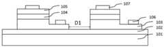
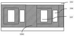
如图1所示,首先选择一临时衬底101,临时衬底101可以是支撑衬底可以是蓝宝石,石英,硅,GaAs,GaN,InP,SiC,GaP,GaSb,AlN和MgO中的一种或多种。As shown in FIG. 1 , a
为了在临时衬底上获得半导体发光元件,首先生长半导体层在临时衬底上或上方获得半导体层,生长工艺可以是MOCVD或液相外延或其它工艺。其中半导体层为多层,并至少包括如下三层,第一导电类型半导体层103、发光层104和第二导电类型半导体层105。其中半导体层可以是为铝镓铟氮、铝镓氮、氮化镓、铝砷化镓、铝镓铟磷或铝铟磷等至少之一种材料。第一导电类型和第二导电类型分别是N、P型导电类型的一种。发光层104在通电情况下提供发光辐射的材料层,具体的可以提供200~950nm波段的辐射,如紫外、蓝光、绿光、黄光、红光、红外等至少一种辐射波段,发光层可以是单量子阱或多量子阱的结构。In order to obtain a semiconductor light-emitting element on a temporary substrate, a semiconductor layer is first grown on or over the temporary substrate, and the growth process may be MOCVD or liquid phase epitaxy or other processes. The semiconductor layer is multi-layered, and includes at least the following three layers, a first conductive
半导体发光元件的半导体层厚度通常为2~10μm或进一步的为5~8μm。The thickness of the semiconductor layer of the semiconductor light-emitting element is usually 2 to 10 μm or further 5 to 8 μm.
作为一个可实施的方式,在制作半导体层之前,临时衬底101的表面侧还可以具有其它的中间层102,其它的中间层102可以辅助分离临时衬底和半导体层的层,如蚀刻截止层或激光剥离层,或提高半导体层生长质量的层,如缓冲层或过度层等,这些层可以在临时衬底与半导体发光元件的半导体层之间分离时同时被去除。As an implementable manner, before the semiconductor layer is fabricated, the surface side of the
如图2所示,对该半导体层进行处理以形成电极结构,其中电极包括第一电极106和第二电极107,分别与第一导电类型半导体层103、第二导电类型半导体层105连接,提供外部电连接至这两层。本实施例中,第一电极106和第二电极107都位于半导体层的同一侧,以提供同一侧的外部电性连接。As shown in FIG. 2, the semiconductor layer is processed to form an electrode structure, wherein the electrodes include a
如图2所示,单元化所述半导体层形成多个半导体发光元件。每相邻的两个半导体发光元件至少侧壁之间是分离的。获得的半导体发光元件侧壁之间暴露一定宽度的槽部,槽部的底部为临时衬底101或中间层102,所述的宽度为D1。As shown in FIG. 2 , the semiconductor layers are unitized to form a plurality of semiconductor light-emitting elements. Every two adjacent semiconductor light emitting elements are separated at least between the side walls. A groove with a certain width is exposed between the sidewalls of the obtained semiconductor light-emitting element, the bottom of the groove is the
优选的,所述的半导体发光元件的水平表面的至少一水平边的宽度小于等于100μm的尺寸,或者所有边水平的宽度小于等于100μm的尺寸,或进一步的介于1~50μm或50~100μm的尺寸。图3为图2所示的结构中从半导体发光元件一侧俯视的结构示意图。Preferably, the width of at least one horizontal side of the horizontal surface of the semiconductor light-emitting element is less than or equal to 100 μm, or the horizontal width of all sides is less than or equal to 100 μm, or further between 1-50 μm or 50-100 μm size. FIG. 3 is a schematic structural diagram of the structure shown in FIG. 2 viewed from the side of the semiconductor light-emitting element.
如图4所示,半导体发光元件还包括一释放层108,所述的释放层108包括两个部分,第一部分位于半导体发光元件的表面侧或属于半导体层中的层,第二部分自第一部分延伸至相邻半导体发光元件之间或者相邻两个半导体发光元件之间并覆盖在槽部的至少部分面上,即释放层的第二部分直接与临时衬底或中间层进行面接触,每相邻两个半导体发光元件的释放层108的第二部分在两者之间是连续未断开的或不连续暴露临时衬底一定的宽度。As shown in FIG. 4 , the semiconductor light-emitting element further includes a
作为一个实施方式,释放层108可以是与半导体发光元件的半导体层中的一层,如为第一导电类型的层或第二导电类型的层的一部分。As an embodiment, the
或者本实施例中,释放层108为额外形成的层,覆盖在半导体发光元件顶表面部分区域和或侧壁,优选的释放层为钝化层或绝缘的透光层,钝化层或透光层具有保护半导体发光元件,防止水汽渗入或防止漏电。释放层优选的为电性绝缘层材料,如氮化物、氧化物或氟化物等透光材料,如氮化硅或氧化硅或氟化镁或氧化钛或氧化镁或氮化钛等至少之一种。优选的,所述的钝化层的折射率低于半导体层。释放层108的第二部分直接覆盖在临时衬底101的表面或中间层102的表面上。Or in this embodiment, the
本实施例中,释放层108的第二部分1082在相邻两个半导体发光元件之间的槽部位置不连续,暴露临时衬底或中间层102的表面一定宽度D2,宽度D2为相邻两半导体发光元件之间的宽度,其中该宽度D2小于宽度D1。In this embodiment, the position of the
释放层108的第二部分1082在半导体发光元件的至少一侧水平延伸一定的宽度D3,此宽度的释放层将用于制作支撑半导体发光元件的桥结构。The
图5为图4所示的结构中从半导体发光元件一侧俯视的结构示意图。FIG. 5 is a schematic structural diagram of the structure shown in FIG. 4 viewed from the side of the semiconductor light emitting element.
释放层108的第二部分1082至少位于半导体发光元件的一侧或两侧或至多半导体发光元件的所有侧面。作为一个可实施的方式,如图5所示,第二部分1082形成在半导体发光元件的两侧。The
释放层108的第二部分1082还包括水平垂直于宽度D2方向的一侧边的宽度D4,D4的宽度大于芯粒相同方向的一侧边的宽度。The
(2)制作支撑结构,形成在每一半导体发光元件的至少一侧,并且支撑结构的底部或侧壁与释放层的延伸部分接触式连接。(2) A support structure is fabricated, which is formed on at least one side of each semiconductor light-emitting element, and the bottom or sidewall of the support structure is connected in contact with the extended portion of the release layer.
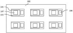
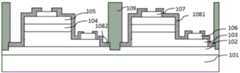
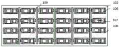
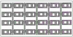
支撑结构109形成在每一半导体发光元件的至少一侧或也可以看成是形成在相邻的半导体发光元件之间。支撑结构109的具体形状可以是支撑柱、支撑台或支撑框架,水平横截面可以是圆形或长方形或正方形或椭圆形等,纵向截面可以是梯形或方形。如图6所示,当支撑结构109为支撑台时,所述的支撑台可以是长条状,其中一个支撑台可以形成在阵列式排列的其中一列的半导体发光元件的一侧或两侧。或者当支撑结构109为支撑柱时,所述的每一半导体发光元件的至少一侧可以形成一个支撑柱。The
支撑结构109的底部形成在每一半导体发光元件的至少一侧或形成在相邻的半导体发光元件之间的临时衬底101上或中间层102上,支撑结构109的侧壁与释放层108的第二部分1082的边缘至少侧壁之间形成接触,或者支撑结构109的底部边缘覆盖在释放层108的第二部分1082的边缘部分之上。支撑结构109与每一半导体发光元件的其余部分无接触连接。支撑结构具体排列方式可以是阵列式或图形分布在阵列式半导体发光元件之间。The bottom of the
支撑结构109需采用硬质材料或可固化成型的材料制作形成,具体可以是金属层、金属合金如AuSn或固化树脂层、环氧树脂、SU-8。The
本实施例中,支撑结构109以固化树脂为例,如BCB或PI或环氧树脂或硅胶,优选的是光敏树脂,采用光刻图形化定义形状,最后加热固化成型形成支撑柱或支撑台。In this embodiment, the
如图7所示,支撑结构109底部形成在中间层102的表面,并沿着半导体发光元件的厚度方向向上延伸至超过半导体发光元件一定的高度H2,所述的H2>0μm,优选≥3μm。支撑结构109与第一电极、第二电极相对于临时衬底101为同一面侧。As shown in FIG. 7 , the bottom of the
支撑结构109具有侧壁与释放层108的第二部分1082的侧边缘接触式连接,并且为了形成稳定且牢固的相互作用,形成支撑结构109后,支撑结构109与释放层108的材料形成接触式连接,两者之间的接触式连接优选为至少形成分子间的作用力,如范德华力的粘黏作用。The
或者,如图8所示,在相邻半导体发光元件之间,所述的支撑结构109形成在中间层102之上,并且底部边缘覆盖到释放层108的第二部分1082的边缘之上表面一定的宽度。由此可以增加支撑结构109与释放层108之间的接触面积以及粘黏作用。Alternatively, as shown in FIG. 8 , between adjacent semiconductor light-emitting elements, the
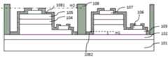
或者,如图9所示,所述的支撑结构109进一步嵌入中间层102或临时衬底101内一定深度,即中间层102本体或进一步的临时衬底101本体被蚀刻一定的深度和宽度形成一槽部,支撑结构109的底部形成在中间层102或临时衬底101的槽部内。支撑结构109的侧壁与释放层的第二部分1082接触式连接。Alternatively, as shown in FIG. 9 , the
(3)粘接一支撑基板在支撑结构的上方。(3) Bonding a support substrate above the support structure.
支撑基板111优选的是刚性材料,对多个半导体发光元件起承载支撑的作用,具体的可选择自蓝宝石、硅、玻璃、金属基板等。The supporting
如图10所示,将支撑基板111覆盖至与支撑结构109的顶部表面,并通过一粘接层粘连两者之间的接触面。在粘接支撑基板之前,如果所述的支撑结构109的材料是固化树脂,所述的支撑结构已经固化成型,因此需通过一额外的粘接层110将两者粘接在一起。此粘接层110可以是金属粘合剂或固化剂如BCB或PI或环氧树脂等材料至少之一种。此粘接层优选先形成在支撑基板的表面,然后通过加热或紫外辐射工艺对粘接层处理以在支撑基板111与支撑结构109之间形成固定成型的粘粘层。优选的在粘接支撑基板与支撑结构时,所述的支撑结构不会发生形变。As shown in FIG. 10 , the
(4)移除临时衬底,获得适于转移的多个半导体发光元件阵列。(4) The temporary substrate is removed to obtain a plurality of semiconductor light-emitting element arrays suitable for transfer.
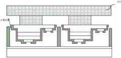
根据临时衬底101的材料性质,可选择激光剥离、湿法蚀刻、研磨等工艺至少一种移除临时衬底。如蓝宝石衬底,可以选择激光剥离技术,临时衬底上可包括一中间层,如缓冲层能够吸收激光并发生分解反应,以分离临时衬底和半导体发光元件。或如砷化镓衬底,可选择湿法蚀刻技术去除,并且较佳的可以提供一蚀刻截止层作为中间层位于砷化镓衬底与半导体发光元件之间,该蚀刻截止层如铝镓铟磷具有相较于砷化镓材料在一蚀刻液中具有更缓慢的蚀刻速率或不发生反应的化学性质,以控制湿法蚀刻截止时间,保护半导体发光元件的一侧半导体层尽量不被蚀刻。According to the material properties of the
去除临时衬底后,与临时衬底或中间层接触的半导体发光元件的表面侧被暴露,本实施例被暴露的是第一导电类型半导体层103表面,以及释放层108的第二部分1082的同一表面侧被暴露。释放层108的第二部分1082被悬空形成桥结构,并且边缘部分连接在支撑结构109侧壁和或部分顶部边缘。After the temporary substrate is removed, the surface side of the semiconductor light emitting element in contact with the temporary substrate or the intermediate layer is exposed. In this embodiment, the surface of the first conductive
如图11所示,适于转移的支撑有多个半导体发光元件阵列的结构具体的包括:支撑基板111;支撑基板111的一面侧具有阵列式的支撑柱或支撑台作为支撑结构109;多个单元化的半导体发光元件,通过释放层形成的桥结构连接支撑结构,半导体发光元件与支撑基板111之间具有空隙,无其它的物理连接位置。As shown in FIG. 11 , a structure suitable for transferring a plurality of semiconductor light-emitting element arrays specifically includes: a supporting
具体的,支撑柱或支撑台与支撑基板之间通过粘接层连接。Specifically, the support column or the support table and the support substrate are connected by an adhesive layer.
具体的,释放层108包括第一部分1081位于每一半导体发光元件表面侧或内部,释放层108包括第二部分1082水平延伸至位于半导体发光元件的至少一侧,第二部分1082的一边缘被连接在支撑结构109的侧壁并且具有一部分长度被悬空形成桥结构,支撑结构109的侧壁与释放层的第二部分1082之间优选通过范德华力的粘黏作用形成连接。Specifically, the
释放层108材料本身具有一定的机械强度,为硬质膜,优选氮化硅或氧化硅这类硬度高的绝缘层,以提供在半导体发光元件与支撑结构稳定的连接以及支撑;在后续半导体发光元件自支撑基板被转移时,所述的释放层108的第二部分1082可在外力作用下,如压力作用下发生断裂,或释放层的第二部分与支撑结构之间的粘连作用在外力的作用下被破坏而发生分离实现转移。The material of the
半导体发光元件除了通过释放层的第二部分形成的桥结构连接支撑柱或支撑台之外,其余的部分被悬空在支撑基板的表面上方,即半导体发光元件与支撑基板或粘接层110之间形成空隙。The semiconductor light-emitting element is suspended above the surface of the support substrate except that the bridge structure formed by the second part of the release layer connects the support column or the support table, that is, between the semiconductor light-emitting element and the support substrate or the
支撑柱或支撑台的顶部高度等于释放层的第二部分1082形成的桥结构的顶部高度。The top height of the support column or support table is equal to the top height of the bridge structure formed by the
图12提供了图11所示结构的俯视图。FIG. 12 provides a top view of the structure shown in FIG. 11 .
或者作为一个变形的实施方式,根据图9的支撑柱或支撑台的类型,最终的适于转移的支撑有多个半导体发光元件阵列的结构上,支撑柱或支撑台的顶部高度可以高于释放层的第二部分形成的桥结构的顶部高度。Or as a variant embodiment, according to the type of the support column or the support table in FIG. 9 , in the final structure suitable for transferring and supporting a plurality of semiconductor light-emitting element arrays, the top height of the support column or the support table can be higher than the release point. The top height of the bridge structure formed by the second portion of the layer.
图13提供了图11的一种替换性的结构类型,其中支撑结构109的顶部边缘被释放层1082的第二部分覆盖并在此处形成连接,连接方式至少包括物理支撑以及包括范德华力的粘黏作用。所述支撑结构的顶部的高度等于所述的释放层108的第二部分形成的桥结构的顶部高度。Figure 13 provides an alternative structure type of Figure 11 in which the top edge of the
本实施例提供了一种制造适于转移的半导体发光元件结构的工艺,采用阵列式或图案化的支撑结构形成在阵列式的半导体发光元件之间,最后通过粘接工艺将阵列式的半导体发光元件转移至支撑基板上,支撑结构与半导体发光元件之间通过释放层的桥结构形成连接。该工艺有效避免使用传统的牺牲层,可避免湿法蚀刻去除牺牲层带来的负面影响,有效提高支撑半导体发光元件阵列结构的良率以及转移的良率。This embodiment provides a process for manufacturing a semiconductor light-emitting element structure suitable for transfer. An array-type or patterned support structure is used to form between the array-type semiconductor light-emitting elements, and finally, the array-type semiconductor light-emitting element is lightened by a bonding process. The element is transferred to the support substrate, and the connection between the support structure and the semiconductor light-emitting element is formed by the bridge structure of the release layer. The process effectively avoids using the traditional sacrificial layer, can avoid the negative influence caused by the removal of the sacrificial layer by wet etching, and effectively improves the yield of the supporting semiconductor light-emitting element array structure and the yield of the transfer.
实施例二Embodiment 2
本实施例作为实施例一的变形实施方式,释放层108在半导体发光元件的至少一侧具有的第二部分1082提供如下改进,该第二部分1082进一步包括宽度变窄的部分。如图15所示,释放层108第二部分具有在半导体发光元件一边侧的平行方向的宽度为D4,D4小于半导体发光元件的同一侧边的宽度,作为一个实施方式,D4的较佳范围为小于等于12μm,优选的是大于等于6μm。This embodiment is a modified implementation of Embodiment 1. The
图16提供了图15所示结构的俯视结构示意图。FIG. 16 provides a schematic top view of the structure shown in FIG. 15 .
其中图17提供了在图15的结构基础上制作支撑结构的结构示意图,本实施例支撑结构109为支撑柱或支撑台,支撑柱或支撑台成型在半导体发光元件至少一侧的临时衬底101或中间层102上,并且支撑柱或支撑台的侧壁与释放层108的第二部分边缘部分接触式连接,优选是粘黏作用,或者支撑柱或支撑台的底部部分覆盖在释放层108的第二部分宽度变窄的边缘部分之上;图18提供了图17所示结构的俯视结构示意图。17 provides a schematic structural diagram of a support structure fabricated on the basis of the structure shown in FIG. 15. In this embodiment, the
图19和20提供了按照实施例一的步骤(4)去除临时衬底后露出的半导体发光元件的表面侧进行俯视的结构示意图。其中释放层108的第二部分端部连接在支撑柱或支撑台109的侧壁上形成悬空的桥结构,由于该第二部分设计为至少部分宽度变窄,因此在后续半导体发光元件在转移过程中,桥结构本身更小宽度更容易断裂或分离。19 and 20 provide schematic structural diagrams of the top view of the surface side of the semiconductor light-emitting element exposed after removing the temporary substrate according to step (4) of the first embodiment. The end of the second part of the
图21作为图13的一种变形实施方式,其中从半导体发光元件的表面侧俯视,释放层108的第二部分1082进一步延伸至覆盖至支撑柱或支撑台109的部分顶部,并且第二部分1082的宽度变窄,形成宽度比半导体发光元件同一侧面的宽度更窄的桥结构。图22提供了相较于图21所示的半导体发元件阵列结构示意图。FIG. 21 is a modified embodiment of FIG. 13 , in which the
实施例三Embodiment 3
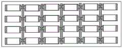
本实施例作为实施例一的变形实施方式,针对释放层108的第二部分1082提供如图23所示的改进,其中半导体发光元件的至少一侧的释放层108的第二部分1082与相邻半导体发光元件之间的释放层108的第二部分1082是连续的,未断开。成型支撑柱或支撑台在半导体发光元件一侧完全覆盖在释放层的第二部分1082之上。This embodiment, as a modified implementation of the first embodiment, provides the improvement shown in FIG. 23 for the
或者作为一种变形实施方式,如图24所示,半导体发光元件的至少一侧的释放层108的第二部分1082与相邻半导体发光元件之间的释放层108的第二部分1082是连续的,未断开,并且释放层的第二部分具有宽度变窄的部分。在第二部分1082宽度变窄的区域之上形成支撑柱或支撑台109获得如图25所示的结构示意图。其中在半导体发光元件的一侧成型的支撑柱或支撑台底部部分覆盖第二部分宽度变窄的部分之上,以及部分覆盖在临时衬底或中间层之上。Or as a variant embodiment, as shown in FIG. 24 , the
图27为图26所示结构的阵列式结构示意图。FIG. 27 is a schematic diagram of an array structure of the structure shown in FIG. 26 .
去除临时衬底后,获得的适用于转移的半导体发光元件的支撑结构如28所示,其中释放层108的第二部分1082被支撑在支撑柱或支撑台的顶部表面,并且支撑结构与释放层的第二部分1082之间形成粘附作用。并且优选的是,释放层的第二部分具有宽度变窄的部分,该宽度变窄的部分用于形成桥结构。After removal of the temporary substrate, the obtained support structure suitable for the transferred semiconductor light emitting element is shown in 28, wherein the
图29为图28所示结构的阵列式结构示意图。FIG. 29 is a schematic diagram of an array structure of the structure shown in FIG. 28 .
实施例四Embodiment 4
作为实施例一至三的变形实施方式,适用于转移的半导体发光元件的支撑结构为支撑框架,具体的支撑框架围绕每一个半导体发光元件设置,所述的释放层在半导体发光元件的至少一侧与支撑框架的顶部和或侧壁接触式连接,所述的连接至少通过范德华力的粘黏作用形成。As a modified implementation of the first to third embodiments, the supporting structure of the semiconductor light-emitting element suitable for transfer is a supporting frame, and the specific supporting frame is arranged around each semiconductor light-emitting element, and the release layer is on at least one side of the semiconductor light-emitting element and The top and/or side walls of the support frame are connected in contact, said connection being formed at least by the adhesive action of van der Waals forces.
具体的以图30所示的结构为例,其提供了图6的所示结构的一种变形实施方式,其中支撑结构109围绕每一半导体发光元件成型为支撑框架(或围坝),释放层108在半导体发光元件至少一侧(本实施例为两侧)具有第二部分1082,成型的支撑框架具有底部或侧壁与释放层108的第二部分形成连接。支撑框架的材料优选地是固化树脂,在粘接支撑基板之前,支撑框架已经固化成型,支撑基板可通过额外的粘接材料粘接在支撑框架的表面侧,去除临时衬底后,半导体发光元件的第一导电类型半导体层103被暴露,从该侧俯视如图31所示,释放层108的第二部分1082从半导体发光元件至少一侧(本实施例为两侧,另外两侧无释放层的第二部分1082,并且中间层110在另外两侧被暴露一部分)与支撑框架的侧壁和或顶部至少通过粘黏作用连接并形成悬空的桥结构。Specifically, the structure shown in FIG. 30 is taken as an example, which provides a modified embodiment of the structure shown in FIG. 6 , wherein the
实施例五Embodiment 5
本实施例提供不同于实施例一至四的一种制作适用于转移的半导体发光元件阵列的工艺以及结构,具体如图32-33所示,首先在临时衬底101或中间层102一面上形成半导体层,半导体层包括第一导电类型半导体层103、第二导电类型半导体层105和发光层104,进一步处理形成第一电极106和第二电极107,并进一步单元化形成多个阵列式的半导体发光元件。单元化的多个半导体发光元件之间侧壁被分离,底部被支撑在临时衬底101或102的一面上。This embodiment provides a process and structure for fabricating a semiconductor light-emitting element array suitable for transfer, which is different from Embodiments 1 to 4. Specifically, as shown in FIGS. 32-33 , a semiconductor is first formed on one side of the
半导体发光元件表面包括一释放层108,至少覆盖在半导体发光元件的顶表面侧,释放层108的材料为绝缘层,保护半导体发光元件,如氮化硅或氧化硅。The surface of the semiconductor light emitting element includes a
然后,形成支撑结构109在半导体发光元件本体顶表面侧的释放层108上。支撑结构109与实施例一为同样的材质,如金属、金属合金或固化树脂,支撑结构109对释放层108具有一定的粘附作用。所述的支撑结构优选图形化工艺形成,更优选的是光刻图形化工艺或者图形化与剥离结合的形成。Then, a
作为一种较佳的实施方式,该释放层109在形成支撑结构的位置优选具有一槽部,槽部的底部优选未露出半导体层,支撑结构形成在该释放层的槽部位置。或者所述的释放层109的表面无槽部,支撑结构直接形成在该释放层的表面侧。支撑结构109的顶部高度高于半导体发光元件的顶部高度。优选的,支撑结构109与半导体发光元件的两个电极位于同一面侧。As a preferred embodiment, the
支撑结构109可以为阵列式的支撑柱或支撑台或图案化的支撑框架。The
然后在支撑结构109的顶部粘接一支撑基板,如图34所示,支撑基板111与支撑结构109之间优选具有一粘接层110。Then, a support substrate is bonded on the top of the
最后去除临时衬底101和中间层102,暴露第一导电类型半导体层103的表面侧,形成如图34所示的适用于转移的半导体发光元件的结构。Finally, the
该适用于转移的支撑有半导体发光元件阵列的结构,包括一支撑基板111,支撑基板上方支撑有阵列式的支撑结构109或图案化的支撑结构,对半导体发光元件形成支撑。支撑结构109与释放层108还可包括其它改变粘附作用的中间层。The structure suitable for transferring a semiconductor light emitting element array includes a
实施例六Embodiment 6
本实施例针对实施例一至五获得的支撑有半导体发光元件阵列的结构上转移半导体发光元件的工艺进行说明,以图11所示的结构为例,从支撑基板上转移单个或多个半导体发光元件时,可采用PDMS转帖技术将一个个的微型尺寸的半导体发光元件可挠式基板或玻璃基板上以制作Micro LED数组,形成显示用的组件。如图35所示,PDMS的转移时,印章112通过范德华力粘贴在半导体发光元件的顶表面侧,然后从印章将压力作用传输到半导体发光元件上,并传输至桥结构,桥结构本身受外力的作用下发生断裂,获得如图36所示的结构示意图,实现半导体发光元件从基板上的转移。或者如图37所示,所述的桥结构与支撑结构之间的粘黏作用在外力的作用下被破坏发生分离,实现对半导体发光元件的转移。This embodiment describes the process of transferring semiconductor light emitting elements on the structure supporting the semiconductor light emitting element array obtained in Examples 1 to 5. Taking the structure shown in FIG. 11 as an example, single or multiple semiconductor light emitting elements are transferred from the supporting substrate. At the same time, the PDMS transfer technology can be used to make micro-sized semiconductor light-emitting elements on flexible substrates or glass substrates to make Micro LED arrays to form components for display. As shown in FIG. 35, when the PDMS is transferred, the
或者以图38所示的结构为例,同样采用PDMS转帖技术转移微型尺寸的半导体发光元件,印章112通过范德华力粘贴在半导体发光元件的顶表面侧,并通过外力的拉扯作用,支撑结构109与释放层108之间的粘附力作用被破坏以实现转移或者支撑结构109本身受外力作用而断裂实现转移。Or take the structure shown in FIG. 38 as an example, the micro-sized semiconductor light-emitting element is also transferred by the PDMS reposting technology, the
实施例七Embodiment 7
作为实施例一到六的一种替代性实施方式,提供如下一种工艺:As an alternative implementation of Embodiments 1 to 6, the following process is provided:
(1)在一临时衬底上获得单元化的多个半导体发光元件,每一半导体发光元件包括一释放层,释放层具有水平的延伸部分位于相邻半导体发光元件之间并覆盖在临时衬底上;(1) Obtaining a plurality of semiconductor light-emitting elements unitized on a temporary substrate, each semiconductor light-emitting element includes a release layer, and the release layer has a horizontal extension portion located between adjacent semiconductor light-emitting elements and covering the temporary substrate superior;
(2)制作阵列式或图案化的支撑结构,形成在支撑基板上;(2) Making an array or patterned support structure on the support substrate;
(3)键合支撑结构在相邻半导体发光元件之间,并且支撑结构的顶部或侧壁与半导体发光元件的释放层的延伸部分之间粘黏,半导体发光元件与支撑基板之间的表面侧悬空;(3) The bonding support structure is between adjacent semiconductor light-emitting elements, and the top or sidewall of the support structure is adhered to the extension of the release layer of the semiconductor light-emitting element, and the surface side between the semiconductor light-emitting element and the support substrate dangling;
(4)移除临时衬底,使释放层的水平延伸部分以及多个半导体发光元件的表面从同一侧被暴露,获得适于转移的支撑基板上支撑的半导体发光元件阵列,其中支撑基板上包括半导体发光元件阵列、支撑结构,释放层的延伸部分与支撑结构连接形成悬空的桥结构。(4) Removing the temporary substrate so that the horizontally extending portion of the release layer and the surfaces of the plurality of semiconductor light-emitting elements are exposed from the same side to obtain a semiconductor light-emitting element array supported on a supporting substrate suitable for transfer, wherein the supporting substrate includes The semiconductor light-emitting element array, the support structure, and the extended part of the release layer are connected with the support structure to form a suspended bridge structure.
该工艺同样有效避免使用牺牲层材料形成适于转移的支撑基板上支撑的半导体发光元件阵列。然而相较于实施例一到六的工艺,该工艺存在对位偏差问题,形成在支撑基板上的支撑结构需要对位半导体发光元件一侧或相邻半导体发光元件之间的位置,并与释放层的延伸部分形成粘黏,该步骤难以实现准确对位。因此,实施例一到六的方式能够避免键合步骤的对位偏差问题,具有更高的制备良率。This process also effectively avoids the use of sacrificial layer materials to form semiconductor light emitting element arrays supported on a transfer substrate suitable for transfer. However, compared with the processes in Embodiments 1 to 6, this process has the problem of alignment deviation, and the support structure formed on the support substrate needs to be aligned with the position on one side of the semiconductor light-emitting element or between adjacent semiconductor light-emitting elements, and is compatible with the release The extended part of the layer forms stickiness, and it is difficult to achieve accurate alignment in this step. Therefore, the methods of Examples 1 to 6 can avoid the problem of alignment deviation in the bonding step, and have a higher production yield.
上述实施例仅例示性说明本发明的原理及其功效,而非用于限制本发明。任何熟悉此技术的人士皆可在不违背本发明的精神及范畴下,对上述实施例进行修饰或改变。因此,举凡所属技术领域中具有通常知识者在未脱离本发明所揭示的精神与技术思想下所完成的一切等效修饰或改变,仍应由本发明的权利要求所涵盖。The above-mentioned embodiments merely illustrate the principles and effects of the present invention, but are not intended to limit the present invention. Anyone skilled in the art can modify or change the above embodiments without departing from the spirit and scope of the present invention. Therefore, all equivalent modifications or changes made by those with ordinary knowledge in the technical field without departing from the spirit and technical idea disclosed in the present invention should still be covered by the claims of the present invention.
Claims (36)
Translated fromChinesePriority Applications (3)
| Application Number | Priority Date | Filing Date | Title |
|---|---|---|---|
| CN201910551455.5ACN112133795B (en) | 2019-06-24 | 2019-06-24 | Method for manufacturing semiconductor light-emitting element structure suitable for transfer |
| CN202210269119.3ACN114664982A (en) | 2019-06-24 | 2019-06-24 | Method for manufacturing semiconductor light-emitting element structure suitable for transfer |
| US16/908,114US11990558B2 (en) | 2019-06-24 | 2020-06-22 | Transferable light emitting device array and production method thereof |
Applications Claiming Priority (1)
| Application Number | Priority Date | Filing Date | Title |
|---|---|---|---|
| CN201910551455.5ACN112133795B (en) | 2019-06-24 | 2019-06-24 | Method for manufacturing semiconductor light-emitting element structure suitable for transfer |
Related Child Applications (1)
| Application Number | Title | Priority Date | Filing Date |
|---|---|---|---|
| CN202210269119.3ADivisionCN114664982A (en) | 2019-06-24 | 2019-06-24 | Method for manufacturing semiconductor light-emitting element structure suitable for transfer |
Publications (2)
| Publication Number | Publication Date |
|---|---|
| CN112133795Atrue CN112133795A (en) | 2020-12-25 |
| CN112133795B CN112133795B (en) | 2022-04-08 |
Family
ID=73849813
Family Applications (2)
| Application Number | Title | Priority Date | Filing Date |
|---|---|---|---|
| CN201910551455.5AActiveCN112133795B (en) | 2019-06-24 | 2019-06-24 | Method for manufacturing semiconductor light-emitting element structure suitable for transfer |
| CN202210269119.3APendingCN114664982A (en) | 2019-06-24 | 2019-06-24 | Method for manufacturing semiconductor light-emitting element structure suitable for transfer |
Family Applications After (1)
| Application Number | Title | Priority Date | Filing Date |
|---|---|---|---|
| CN202210269119.3APendingCN114664982A (en) | 2019-06-24 | 2019-06-24 | Method for manufacturing semiconductor light-emitting element structure suitable for transfer |
Country Status (2)
| Country | Link |
|---|---|
| US (1) | US11990558B2 (en) |
| CN (2) | CN112133795B (en) |
Cited By (8)
| Publication number | Priority date | Publication date | Assignee | Title |
|---|---|---|---|---|
| CN112750935A (en)* | 2020-12-31 | 2021-05-04 | 深圳市思坦科技有限公司 | LED chip and manufacturing method thereof |
| CN114156222A (en)* | 2021-11-29 | 2022-03-08 | 京东方科技集团股份有限公司 | Transfer substrate, light-emitting substrate and preparation method thereof, and display device |
| CN115084333A (en)* | 2022-05-10 | 2022-09-20 | 南昌大学 | Inverted GaN-based Micro-LED display module and preparation method thereof |
| CN115172246A (en)* | 2022-02-22 | 2022-10-11 | 京东方科技集团股份有限公司 | Device transfer substrate, manufacturing method thereof and device transfer method |
| WO2023005672A1 (en)* | 2021-07-26 | 2023-02-02 | 重庆康佳光电技术研究院有限公司 | Growth substrate assembly and manufacturing method therefor, and manufacturing method for light-emitting assembly |
| CN115763349A (en)* | 2022-04-01 | 2023-03-07 | 友达光电股份有限公司 | Light-emitting panel |
| WO2023092594A1 (en)* | 2021-11-29 | 2023-06-01 | 京东方科技集团股份有限公司 | Light-emitting substrate and preparation method therefor, and display device |
| US11984544B2 (en) | 2021-05-26 | 2024-05-14 | Lextar Electronics Corporation | Light-emitting element and display device using the same |
Families Citing this family (7)
| Publication number | Priority date | Publication date | Assignee | Title |
|---|---|---|---|---|
| US20230178611A1 (en)* | 2014-12-23 | 2023-06-08 | Kyocera Sld Laser, Inc. | Manufacturable gallium containing electronic devices |
| US20220384688A1 (en)* | 2017-08-30 | 2022-12-01 | Xiamen San'an Optoelectronics Co., Ltd. | Micro light-emitting diode and micro light-emitting diode array |
| CN109860364B (en)* | 2017-08-30 | 2020-09-01 | 天津三安光电有限公司 | Light emitting diode |
| US11296269B2 (en)* | 2020-07-30 | 2022-04-05 | Lextar Electronics Corporation | Light emitting diode packaging structure and method for manufacturing the same |
| CN113054074B (en)* | 2021-03-01 | 2022-04-22 | 康佳集团股份有限公司 | A Mass Transfer Method for LED Chips |
| JP7739964B2 (en)* | 2021-11-17 | 2025-09-17 | 沖電気工業株式会社 | Method for manufacturing electronic structure and electronic circuit |
| US12400883B2 (en)* | 2022-03-23 | 2025-08-26 | Vanguard International Semiconductor Corporation | Structure of transferring dies for use in mass transferring process |
Citations (8)
| Publication number | Priority date | Publication date | Assignee | Title |
|---|---|---|---|---|
| US8558243B2 (en)* | 2011-11-18 | 2013-10-15 | LuxVue Technology Corporation | Micro device array for transfer to a receiving substrate |
| CN107579141A (en)* | 2017-07-24 | 2018-01-12 | 友达光电股份有限公司 | Micro light-emitting element and manufacturing method thereof, display device and transition carrier plate device |
| WO2018035668A1 (en)* | 2016-08-22 | 2018-03-01 | Goertek.Inc | Micro-led transfer method, manufacturing method and device |
| CN107818931A (en)* | 2017-09-30 | 2018-03-20 | 厦门市三安光电科技有限公司 | The transfer method and transfer device of semiconductor microactuator element |
| CN107933064A (en)* | 2017-11-10 | 2018-04-20 | 上海天马微电子有限公司 | Transfer printing substrate and manufacturing method thereof |
| CN108417682A (en)* | 2018-03-22 | 2018-08-17 | 厦门市三安光电科技有限公司 | A kind of miniature light-emitting element and its manufacturing method |
| US20190088526A1 (en)* | 2016-11-15 | 2019-03-21 | X-Celeprint Limited | Micro-transfer-printable flip-chip structures and methods |
| US20190115503A1 (en)* | 2017-10-16 | 2019-04-18 | PlayNitride Inc. | Structure with micro light-emitting device |
Family Cites Families (7)
| Publication number | Priority date | Publication date | Assignee | Title |
|---|---|---|---|---|
| US9768345B2 (en)* | 2013-12-20 | 2017-09-19 | Apple Inc. | LED with current injection confinement trench |
| US9583466B2 (en)* | 2013-12-27 | 2017-02-28 | Apple Inc. | Etch removal of current distribution layer for LED current confinement |
| KR102382886B1 (en)* | 2015-05-26 | 2022-04-05 | 쑤저우 레킨 세미컨덕터 컴퍼니 리미티드 | Light emitting device |
| FR3037612B1 (en)* | 2015-06-17 | 2017-06-09 | Ene29 S Ar L | SEISMIC WAVE GENERATION TOOL AS AN ECLATOR OF A DEVICE FOR GENERATING ELECTRIC ARCS |
| WO2017030396A1 (en)* | 2015-08-18 | 2017-02-23 | 엘지이노텍(주) | Light-emitting element, light-emitting element package comprising light-emitting element, and light-emitting device comprising light-emitting element package |
| WO2018137139A1 (en)* | 2017-01-24 | 2018-08-02 | Goertek. Inc | Micro-led device, display apparatus and method for manufacturing a micro-led device |
| TWI626766B (en)* | 2017-06-01 | 2018-06-11 | 錼創科技股份有限公司 | Light-emitting element |
- 2019
- 2019-06-24CNCN201910551455.5Apatent/CN112133795B/enactiveActive
- 2019-06-24CNCN202210269119.3Apatent/CN114664982A/enactivePending
- 2020
- 2020-06-22USUS16/908,114patent/US11990558B2/enactiveActive
Patent Citations (8)
| Publication number | Priority date | Publication date | Assignee | Title |
|---|---|---|---|---|
| US8558243B2 (en)* | 2011-11-18 | 2013-10-15 | LuxVue Technology Corporation | Micro device array for transfer to a receiving substrate |
| WO2018035668A1 (en)* | 2016-08-22 | 2018-03-01 | Goertek.Inc | Micro-led transfer method, manufacturing method and device |
| US20190088526A1 (en)* | 2016-11-15 | 2019-03-21 | X-Celeprint Limited | Micro-transfer-printable flip-chip structures and methods |
| CN107579141A (en)* | 2017-07-24 | 2018-01-12 | 友达光电股份有限公司 | Micro light-emitting element and manufacturing method thereof, display device and transition carrier plate device |
| CN107818931A (en)* | 2017-09-30 | 2018-03-20 | 厦门市三安光电科技有限公司 | The transfer method and transfer device of semiconductor microactuator element |
| US20190115503A1 (en)* | 2017-10-16 | 2019-04-18 | PlayNitride Inc. | Structure with micro light-emitting device |
| CN107933064A (en)* | 2017-11-10 | 2018-04-20 | 上海天马微电子有限公司 | Transfer printing substrate and manufacturing method thereof |
| CN108417682A (en)* | 2018-03-22 | 2018-08-17 | 厦门市三安光电科技有限公司 | A kind of miniature light-emitting element and its manufacturing method |
Cited By (10)
| Publication number | Priority date | Publication date | Assignee | Title |
|---|---|---|---|---|
| CN112750935A (en)* | 2020-12-31 | 2021-05-04 | 深圳市思坦科技有限公司 | LED chip and manufacturing method thereof |
| CN112750935B (en)* | 2020-12-31 | 2022-03-15 | 深圳市思坦科技有限公司 | A kind of LED chip and its production method |
| US11984544B2 (en) | 2021-05-26 | 2024-05-14 | Lextar Electronics Corporation | Light-emitting element and display device using the same |
| WO2023005672A1 (en)* | 2021-07-26 | 2023-02-02 | 重庆康佳光电技术研究院有限公司 | Growth substrate assembly and manufacturing method therefor, and manufacturing method for light-emitting assembly |
| CN114156222A (en)* | 2021-11-29 | 2022-03-08 | 京东方科技集团股份有限公司 | Transfer substrate, light-emitting substrate and preparation method thereof, and display device |
| WO2023092594A1 (en)* | 2021-11-29 | 2023-06-01 | 京东方科技集团股份有限公司 | Light-emitting substrate and preparation method therefor, and display device |
| CN114156222B (en)* | 2021-11-29 | 2024-09-24 | 京东方科技集团股份有限公司 | Transfer substrate, light-emitting substrate and preparation method thereof, and display device |
| CN115172246A (en)* | 2022-02-22 | 2022-10-11 | 京东方科技集团股份有限公司 | Device transfer substrate, manufacturing method thereof and device transfer method |
| CN115763349A (en)* | 2022-04-01 | 2023-03-07 | 友达光电股份有限公司 | Light-emitting panel |
| CN115084333A (en)* | 2022-05-10 | 2022-09-20 | 南昌大学 | Inverted GaN-based Micro-LED display module and preparation method thereof |
Also Published As
| Publication number | Publication date |
|---|---|
| US11990558B2 (en) | 2024-05-21 |
| US20200403114A1 (en) | 2020-12-24 |
| CN114664982A (en) | 2022-06-24 |
| CN112133795B (en) | 2022-04-08 |
Similar Documents
| Publication | Publication Date | Title |
|---|---|---|
| CN112133795B (en) | Method for manufacturing semiconductor light-emitting element structure suitable for transfer | |
| CN109817767B (en) | Micro device and manufacturing method thereof | |
| US11791446B2 (en) | Micro-device with strengthened connecting layers | |
| CN118160065A (en) | Method for manufacturing bonded semiconductor wafer | |
| TWI482309B (en) | Thin film light-emitting diode with P contact and N contact electrically insulated from the substrate | |
| TWI413273B (en) | Packaged integrated film light-emitting diode | |
| CN108550667B (en) | A kind of miniature light-emitting element and its manufacturing method | |
| JP5590837B2 (en) | Relocation of functional areas | |
| WO2018091459A4 (en) | Micro-transfer-printable flip-chip structures and methods | |
| CN102646763B (en) | The manufacture method of nitride semiconductor luminescent element | |
| CN112750851B (en) | Micro light-emitting element array substrate, preparation method and transfer method | |
| JP7136311B1 (en) | Bonded semiconductor wafer manufacturing method | |
| CN112864287B (en) | Transfer method, micro device array and preparation method thereof | |
| WO2014110982A1 (en) | Laser lift-off-based method for preparing semiconductor light-emitting device | |
| CN115425122B (en) | LED chip mass transfer method and display panel | |
| CN110088919A (en) | Light emitting element, light emitting element array and light emitting device | |
| CN119032430A (en) | Light emitting element and method for manufacturing the same | |
| JP7701319B2 (en) | Manufacturing method of bonded wafer for micro LED | |
| TWI452621B (en) | Separation method of epitaxial element | |
| CN115172246A (en) | Device transfer substrate, manufacturing method thereof and device transfer method | |
| JP7367743B2 (en) | Manufacturing method of bonded semiconductor wafer | |
| CN117352631A (en) | Micro-LED chip array with surface Micro lenses and preparation method thereof | |
| CN118476042A (en) | Wafer with micro LED structure, method for manufacturing wafer with micro LED structure, and method for manufacturing bonded semiconductor wafer with micro LED structure | |
| CN120529726A (en) | Preparation method of Micro LED display module and display device | |
| CN114792631A (en) | Method for wafer bonding and compound semiconductor wafer |
Legal Events
| Date | Code | Title | Description |
|---|---|---|---|
| PB01 | Publication | ||
| PB01 | Publication | ||
| SE01 | Entry into force of request for substantive examination | ||
| SE01 | Entry into force of request for substantive examination | ||
| GR01 | Patent grant | ||
| GR01 | Patent grant |