CN112119447A - Data distribution for holographic projection - Google Patents
Data distribution for holographic projectionDownload PDFInfo
- Publication number
- CN112119447A CN112119447ACN201980032531.XACN201980032531ACN112119447ACN 112119447 ACN112119447 ACN 112119447ACN 201980032531 ACN201980032531 ACN 201980032531ACN 112119447 ACN112119447 ACN 112119447A
- Authority
- CN
- China
- Prior art keywords
- data
- control
- input data
- delay line
- pixel elements
- Prior art date
- Legal status (The legal status is an assumption and is not a legal conclusion. Google has not performed a legal analysis and makes no representation as to the accuracy of the status listed.)
- Granted
Links
- 238000009826distributionMethods0.000titledescription84
- 238000000034methodMethods0.000claimsabstractdescription18
- 230000001360synchronised effectEffects0.000claimsabstractdescription12
- 238000012805post-processingMethods0.000claimsdescription29
- 230000005540biological transmissionEffects0.000claimsdescription18
- 238000013461designMethods0.000claimsdescription18
- 230000001902propagating effectEffects0.000claimsdescription14
- 238000003860storageMethods0.000claimsdescription12
- 239000010409thin filmSubstances0.000claimsdescription4
- 238000004364calculation methodMethods0.000claimsdescription3
- 238000000638solvent extractionMethods0.000claims1
- 238000001514detection methodMethods0.000abstractdescription6
- 230000008901benefitEffects0.000description44
- 239000010410layerSubstances0.000description19
- 239000000463materialSubstances0.000description13
- 238000005516engineering processMethods0.000description9
- 230000000670limiting effectEffects0.000description9
- 239000012782phase change materialSubstances0.000description9
- 239000012071phaseSubstances0.000description7
- 239000000758substrateSubstances0.000description7
- 230000002829reductive effectEffects0.000description6
- 230000003068static effectEffects0.000description6
- 238000012546transferMethods0.000description6
- 230000036961partial effectEffects0.000description5
- 239000004065semiconductorSubstances0.000description5
- 239000000243solutionSubstances0.000description5
- XLOMVQKBTHCTTD-UHFFFAOYSA-NZinc monoxideChemical compound[Zn]=OXLOMVQKBTHCTTD-UHFFFAOYSA-N0.000description4
- 230000009471actionEffects0.000description4
- 230000008859changeEffects0.000description4
- 238000012937correctionMethods0.000description4
- 230000001419dependent effectEffects0.000description4
- 230000008447perceptionEffects0.000description4
- 230000008569processEffects0.000description4
- 230000001960triggered effectEffects0.000description4
- 238000010586diagramMethods0.000description3
- 230000006870functionEffects0.000description3
- 230000004048modificationEffects0.000description3
- 238000012986modificationMethods0.000description3
- 230000009467reductionEffects0.000description3
- 230000004044responseEffects0.000description3
- 238000004088simulationMethods0.000description3
- 239000002356single layerSubstances0.000description3
- OKTJSMMVPCPJKN-UHFFFAOYSA-NCarbonChemical compound[C]OKTJSMMVPCPJKN-UHFFFAOYSA-N0.000description2
- GYHNNYVSQQEPJS-UHFFFAOYSA-NGalliumChemical compound[Ga]GYHNNYVSQQEPJS-UHFFFAOYSA-N0.000description2
- 238000003491arrayMethods0.000description2
- 239000002131composite materialSubstances0.000description2
- 150000001875compoundsChemical class0.000description2
- 230000008878couplingEffects0.000description2
- 238000010168coupling processMethods0.000description2
- 238000005859coupling reactionMethods0.000description2
- 238000013144data compressionMethods0.000description2
- 230000000694effectsEffects0.000description2
- 229910052733galliumInorganic materials0.000description2
- 229910021389grapheneInorganic materials0.000description2
- 229910052738indiumInorganic materials0.000description2
- APFVFJFRJDLVQX-UHFFFAOYSA-Nindium atomChemical compound[In]APFVFJFRJDLVQX-UHFFFAOYSA-N0.000description2
- 238000002347injectionMethods0.000description2
- 239000007924injectionSubstances0.000description2
- 238000004519manufacturing processMethods0.000description2
- 239000011159matrix materialSubstances0.000description2
- 229910052751metalInorganic materials0.000description2
- 239000002184metalSubstances0.000description2
- 230000003287optical effectEffects0.000description2
- 229910052710siliconInorganic materials0.000description2
- 239000010703siliconSubstances0.000description2
- 239000007787solidSubstances0.000description2
- 230000002123temporal effectEffects0.000description2
- 230000009466transformationEffects0.000description2
- 238000013519translationMethods0.000description2
- 239000011787zinc oxideSubstances0.000description2
- XUIMIQQOPSSXEZ-UHFFFAOYSA-NSiliconChemical compound[Si]XUIMIQQOPSSXEZ-UHFFFAOYSA-N0.000description1
- 238000010521absorption reactionMethods0.000description1
- WYTGDNHDOZPMIW-RCBQFDQVSA-NalstonineNatural productsC1=CC2=C3C=CC=CC3=NC2=C2N1C[C@H]1[C@H](C)OC=C(C(=O)OC)[C@H]1C2WYTGDNHDOZPMIW-RCBQFDQVSA-N0.000description1
- 238000005452bendingMethods0.000description1
- 230000009286beneficial effectEffects0.000description1
- 239000000872bufferSubstances0.000description1
- 239000003990capacitorSubstances0.000description1
- 230000000295complement effectEffects0.000description1
- 238000007906compressionMethods0.000description1
- 230000006835compressionEffects0.000description1
- 238000013501data transformationMethods0.000description1
- 238000011982device technologyMethods0.000description1
- 230000005284excitationEffects0.000description1
- 230000001747exhibiting effectEffects0.000description1
- 239000004744fabricSubstances0.000description1
- 239000012530fluidSubstances0.000description1
- 238000005286illuminationMethods0.000description1
- 238000003780insertionMethods0.000description1
- 230000037431insertionEffects0.000description1
- 230000003993interactionEffects0.000description1
- 239000004973liquid crystal related substanceSubstances0.000description1
- 230000007774longtermEffects0.000description1
- 238000005259measurementMethods0.000description1
- 230000006386memory functionEffects0.000description1
- 238000001465metallisationMethods0.000description1
- 238000004377microelectronicMethods0.000description1
- 230000003278mimic effectEffects0.000description1
- 239000000382optic materialSubstances0.000description1
- 230000008520organizationEffects0.000description1
- 230000000737periodic effectEffects0.000description1
- 238000012545processingMethods0.000description1
- 238000002310reflectometryMethods0.000description1
- 238000009877renderingMethods0.000description1
- 230000000717retained effectEffects0.000description1
- 230000000630rising effectEffects0.000description1
- 230000001953sensory effectEffects0.000description1
- 230000001568sexual effectEffects0.000description1
- 239000007790solid phaseSubstances0.000description1
- 238000000844transformationMethods0.000description1
- 238000002834transmittanceMethods0.000description1
- 230000005641tunnelingEffects0.000description1
- TYHJXGDMRRJCRY-UHFFFAOYSA-Nzinc indium(3+) oxygen(2-) tin(4+)Chemical compound[O-2].[Zn+2].[Sn+4].[In+3]TYHJXGDMRRJCRY-UHFFFAOYSA-N0.000description1
Images


Classifications
- G—PHYSICS
- G09—EDUCATION; CRYPTOGRAPHY; DISPLAY; ADVERTISING; SEALS
- G09G—ARRANGEMENTS OR CIRCUITS FOR CONTROL OF INDICATING DEVICES USING STATIC MEANS TO PRESENT VARIABLE INFORMATION
- G09G3/00—Control arrangements or circuits, of interest only in connection with visual indicators other than cathode-ray tubes
- G09G3/20—Control arrangements or circuits, of interest only in connection with visual indicators other than cathode-ray tubes for presentation of an assembly of a number of characters, e.g. a page, by composing the assembly by combination of individual elements arranged in a matrix no fixed position being assigned to or needed to be assigned to the individual characters or partial characters
- G—PHYSICS
- G09—EDUCATION; CRYPTOGRAPHY; DISPLAY; ADVERTISING; SEALS
- G09G—ARRANGEMENTS OR CIRCUITS FOR CONTROL OF INDICATING DEVICES USING STATIC MEANS TO PRESENT VARIABLE INFORMATION
- G09G3/00—Control arrangements or circuits, of interest only in connection with visual indicators other than cathode-ray tubes
- G09G3/001—Control arrangements or circuits, of interest only in connection with visual indicators other than cathode-ray tubes using specific devices not provided for in groups G09G3/02 - G09G3/36, e.g. using an intermediate record carrier such as a film slide; Projection systems; Display of non-alphanumerical information, solely or in combination with alphanumerical information, e.g. digital display on projected diapositive as background
- G09G3/003—Control arrangements or circuits, of interest only in connection with visual indicators other than cathode-ray tubes using specific devices not provided for in groups G09G3/02 - G09G3/36, e.g. using an intermediate record carrier such as a film slide; Projection systems; Display of non-alphanumerical information, solely or in combination with alphanumerical information, e.g. digital display on projected diapositive as background to produce spatial visual effects
- G—PHYSICS
- G09—EDUCATION; CRYPTOGRAPHY; DISPLAY; ADVERTISING; SEALS
- G09G—ARRANGEMENTS OR CIRCUITS FOR CONTROL OF INDICATING DEVICES USING STATIC MEANS TO PRESENT VARIABLE INFORMATION
- G09G3/00—Control arrangements or circuits, of interest only in connection with visual indicators other than cathode-ray tubes
- G09G3/20—Control arrangements or circuits, of interest only in connection with visual indicators other than cathode-ray tubes for presentation of an assembly of a number of characters, e.g. a page, by composing the assembly by combination of individual elements arranged in a matrix no fixed position being assigned to or needed to be assigned to the individual characters or partial characters
- G09G3/2085—Special arrangements for addressing the individual elements of the matrix, other than by driving respective rows and columns in combination
- G—PHYSICS
- G03—PHOTOGRAPHY; CINEMATOGRAPHY; ANALOGOUS TECHNIQUES USING WAVES OTHER THAN OPTICAL WAVES; ELECTROGRAPHY; HOLOGRAPHY
- G03H—HOLOGRAPHIC PROCESSES OR APPARATUS
- G03H1/00—Holographic processes or apparatus using light, infrared or ultraviolet waves for obtaining holograms or for obtaining an image from them; Details peculiar thereto
- G03H1/04—Processes or apparatus for producing holograms
- G—PHYSICS
- G09—EDUCATION; CRYPTOGRAPHY; DISPLAY; ADVERTISING; SEALS
- G09G—ARRANGEMENTS OR CIRCUITS FOR CONTROL OF INDICATING DEVICES USING STATIC MEANS TO PRESENT VARIABLE INFORMATION
- G09G2310/00—Command of the display device
- G09G2310/02—Addressing, scanning or driving the display screen or processing steps related thereto
- G09G2310/0202—Addressing of scan or signal lines
- G09G2310/0213—Addressing of scan or signal lines controlling the sequence of the scanning lines with respect to the patterns to be displayed, e.g. to save power
- G—PHYSICS
- G09—EDUCATION; CRYPTOGRAPHY; DISPLAY; ADVERTISING; SEALS
- G09G—ARRANGEMENTS OR CIRCUITS FOR CONTROL OF INDICATING DEVICES USING STATIC MEANS TO PRESENT VARIABLE INFORMATION
- G09G2310/00—Command of the display device
- G09G2310/02—Addressing, scanning or driving the display screen or processing steps related thereto
- G09G2310/0264—Details of driving circuits
- G09G2310/0297—Special arrangements with multiplexing or demultiplexing of display data in the drivers for data electrodes, in a pre-processing circuitry delivering display data to said drivers or in the matrix panel, e.g. multiplexing plural data signals to one D/A converter or demultiplexing the D/A converter output to multiple columns
- G—PHYSICS
- G09—EDUCATION; CRYPTOGRAPHY; DISPLAY; ADVERTISING; SEALS
- G09G—ARRANGEMENTS OR CIRCUITS FOR CONTROL OF INDICATING DEVICES USING STATIC MEANS TO PRESENT VARIABLE INFORMATION
- G09G2310/00—Command of the display device
- G09G2310/04—Partial updating of the display screen
Landscapes
- Engineering & Computer Science (AREA)
- Physics & Mathematics (AREA)
- General Physics & Mathematics (AREA)
- Computer Hardware Design (AREA)
- Theoretical Computer Science (AREA)
- Control Of Indicators Other Than Cathode Ray Tubes (AREA)
- Liquid Crystal Display Device Control (AREA)
- Devices For Indicating Variable Information By Combining Individual Elements (AREA)
Abstract
Description
Translated fromChinese发明领域Field of Invention
本发明一般涉及能量高效的数据分发系统和方法,并且尤其涉及用于全息光投影设备中的部分显示更新的数据分发系统和方法。The present invention relates generally to energy efficient data distribution systems and methods, and more particularly to data distribution systems and methods for partial display updates in holographic light projection devices.
背景技术Background technique
在常规的显示器应用中,像素值以逐行方式被周期性地刷新。在给定视频内容数据的新帧的情况下更新显示由此需要对显示区域进行完整扫描,这需要停滞时间,在此期间不能更新显示的像素值,并且需要花费大量能量将新的视频内容数据帧分发和上传到所有显示器像素。因此,需要一种性能良好的底层数据分发硬件,该硬件可以应付对接收到的输入视频数据流中的大量数据的及时且能量高效的分发和更新。这在具有需要定期更新的大量像素的高分辨率显示器的情形中特别重要,并且在提供增强的观看舒适性和能力的紧凑型显示器(例如,立体显示器或3D显示器,诸如以大的视角为单名观众或多名观众提供深度感知的3D光场显示器或全息显示器)中更为重要。In conventional display applications, pixel values are periodically refreshed on a line-by-line basis. Updating the display given a new frame of video content data thus requires a full scan of the display area, which requires dead time during which the displayed pixel values cannot be updated, and expends a lot of energy to convert the new video content data Frame distribution and upload to all display pixels. Therefore, there is a need for a well-performing underlying data distribution hardware that can handle the timely and energy-efficient distribution and updating of large amounts of data in received input video data streams. This is particularly important in the case of high-resolution displays with a large number of pixels that need to be updated regularly, and in compact displays that provide enhanced viewing comfort and capability (eg, stereoscopic displays or 3D displays, such as monolithic displays with large viewing angles) more important in 3D light field displays or holographic displays that provide depth perception to one or more viewers.
用于数据分发或用于对数据的动态寻址(用于写入和读取)的系统的已知示例是交叉开关设计或DRAM存储器访问技术。对于前者,开关组件的数目呈二次方增长,并且在扩大访问带宽时不提供足够能量高效的解决方案;后者通常并发地覆写整个行,即使仅一个数据位置需要更新亦如此。此外,至少对于易失性CMOS设计而言,分布式存储的数据需要定期(通常在毫秒范围中)刷新。因此,存在对尽可能节省资源并且还具有高吞吐量和低更新等待时间的特征的解决方案的需求。Known examples of systems for data distribution or for dynamic addressing of data (for writing and reading) are crossbar designs or DRAM memory access techniques. For the former, the number of switch components grows quadratically and does not provide a sufficiently energy-efficient solution when expanding access bandwidth; the latter typically overwrites entire rows concurrently, even if only one data location needs to be updated. Furthermore, at least for volatile CMOS designs, distributed stored data needs to be refreshed periodically (usually in the millisecond range). Therefore, there is a need for a solution that saves resources as much as possible and also features high throughput and low update latency.
发明内容SUMMARY OF THE INVENTION
本发明的各实施例的目的在于提供一种用于分发数据以供3D光场和全息投影的高效、高吞吐量-低等待时间系统。It is an object of embodiments of the present invention to provide an efficient, high throughput-low latency system for distributing data for 3D light field and holographic projection.
以上目的由根据本发明的方法和设备来实现。The above objects are achieved by the method and apparatus according to the present invention.
在第一方面,本发明涉及一种用于分发数据以供3D光场投影的系统。该系统包括适合于接收输入数据流的多个输入端子,以及能连接到显示器的像素元件的多个输出端子。多条数据路径存在于输入端子与输出端子之间,并且多个数据开关适合于在输入端子处接收到输入数据时经由控制变量来控制该输入数据在数据路径上的传输。用于分发数据的系统进一步包括控制平面,该控制平面被适配成用于将控制变量应用于数据开关。该控制平面包括多个控制开关,该多个控制开关用于经由使能变量从控制变量序列中选择一个或多个控制变量并用于将该一个或多个控制变量应用于数据开关。该控制平面中还包括适合于传播控制变量序列的至少一条第一延迟线、以及适合于传播使能变量序列的至少一条第二延迟线。该至少一条第一延迟线和该至少一条第二延迟线各自包括一个或多个延迟单元。该至少一条第一延迟线中的该一个或多个延迟单元中的每个延迟单元与该至少一条第二延迟线中的该一个或多个延迟单元中的恰好一个延迟单元处于同步关系。用于分发数据的系统还包括:用于在系统运行时期间接收到输入数据流时检测该输入数据流中所包含的模式的装置。所检测到的模式确定控制变量序列。In a first aspect, the present invention relates to a system for distributing data for 3D light field projection. The system includes a plurality of input terminals adapted to receive an input data stream, and a plurality of output terminals connectable to pixel elements of a display. A plurality of data paths exist between the input terminal and the output terminal, and a plurality of data switches are adapted to control the transmission of input data on the data paths via control variables when the input data is received at the input terminals. The system for distributing data further includes a control plane adapted to apply control variables to the data switches. The control plane includes a plurality of control switches for selecting one or more control variables from a sequence of control variables via an enable variable and for applying the one or more control variables to a data switch. Also included in the control plane are at least one first delay line suitable for propagating the sequence of control variables, and at least one second delay line suitable for propagating the sequence of enabling variables. The at least one first delay line and the at least one second delay line each include one or more delay cells. Each delay cell of the one or more delay cells in the at least one first delay line is in a synchronous relationship with exactly one delay cell of the one or more delay cells in the at least one second delay line. The system for distributing data also includes means for detecting patterns contained in the incoming data stream when the incoming data stream is received during system runtime. The detected patterns determine the sequence of control variables.
本发明的各实施例的优点在于,对控制变量的选择提供对被应用于显示器的可连接像素元件的全息图像数据的部分更新,由此减少每面积单位能量开销。An advantage of embodiments of the present invention is that selection of control variables provides partial updates to holographic image data applied to connectable pixel elements of the display, thereby reducing energy per area unit overhead.
优点还在于,控制变量是在具有较低电容负载和较短等待时间的短延迟线上依次发送的。The advantage is also that the control variables are sent sequentially on short delay lines with lower capacitive loading and shorter latency.
本发明的各实施例的优点在于,控制变量或整个控制序列可以被存储在数据开关上达较长时间而不被刷新。An advantage of embodiments of the present invention is that control variables or entire control sequences can be stored on data switches for extended periods of time without being refreshed.
在本发明的一些实施例中,用于检测模式的装置可以包括运行时引擎,该运行时引擎决定对控制平面的更新模式的选择,这有利地影响对系统的能量高效使用。In some embodiments of the invention, the means for detecting a mode may include a runtime engine that determines the selection of an update mode for the control plane, which beneficially affects the energy efficient use of the system.
本发明的各实施例的优点在于,控制平面设计减少了路由开销,从而提供能量和面积高效的数据分发系统。An advantage of embodiments of the present invention is that the control plane design reduces routing overhead, thereby providing an energy and area efficient data distribution system.
本发明的各实施例的优点在于,高输入数据量话务由系统处置并且实现高吞吐率。An advantage of embodiments of the present invention is that high incoming data volume traffic is handled by the system and high throughput rates are achieved.
根据本发明的一些实施例,用于分发数据的系统进一步包括:用于对针对该多个输出端子中的至少一个输出端子所传输的输入数据执行本地后处理计算的装置。According to some embodiments of the present invention, the system for distributing data further comprises: means for performing local post-processing computations on input data transmitted for at least one output terminal of the plurality of output terminals.
在本发明的特定实施例中,用于执行本地后处理计算的装置可以包括对所传输的输入数据进行操作的本地数据解码器。In certain embodiments of the invention, the means for performing local post-processing computations may include a local data decoder that operates on the transmitted input data.
在本发明的其他实施例中,用于执行本地后处理计算的装置可包括:用于标识针对该多个输出端子中的至少一个输出端子新近传输的输入数据与先前传输到该输出端子的输入数据相比是否已改变的电路。In other embodiments of the invention, the means for performing local post-processing computations may include: for identifying newly transmitted input data for at least one output terminal of the plurality of output terminals from inputs previously transmitted to the output terminal whether the data has changed compared to the circuit.
对于本发明的一些实施例,用于检测模式的装置还可以被适配成控制对本地后处理计算的执行。For some embodiments of the invention, the means for detecting patterns may also be adapted to control the execution of local post-processing computations.
本发明的一些实施例的优点在于,本地后处理计算可以在本地级别并以分布式方式执行。这允许更多的后处理功能性以及增加的像素级控制。An advantage of some embodiments of the present invention is that local post-processing computations can be performed at the local level and in a distributed fashion. This allows for more post-processing functionality and increased pixel-level control.
本发明的一些实施例的优点在于,本地解码装置可以减少输入数据传输所必需的导线数目,并借助输入数据压缩允许对输入数据更加紧凑的表示。因此可实现较高的输入数据吞吐率。An advantage of some embodiments of the present invention is that the local decoding device can reduce the number of wires necessary for input data transmission and allow for a more compact representation of the input data with input data compression. Therefore, a higher input data throughput rate can be achieved.
本发明的一些实施例的优点在于,可以在本地实现许多器件而不需要锁存器或寄存器(例如,在CMOS逻辑中的情形),并且许多器件可以以分布式方式彼此独立地执行后处理计算。An advantage of some embodiments of the present invention is that many devices can be implemented locally without the need for latches or registers (eg, as is the case in CMOS logic), and that many devices can perform post-processing computations independently of each other in a distributed fashion .
本发明的一些实施例的优点在于,在本地重用已传输的输入数据。因此,可以避免将输入数据冗余地写入到像素元件,并且数据分发系统以更加能量高效的方式操作。An advantage of some embodiments of the present invention is that the transmitted input data is reused locally. Thus, redundant writing of input data to pixel elements can be avoided and the data distribution system operates in a more energy efficient manner.
根据本发明的一些实施例,该至少一条第一延迟线中的该一个或多个延迟单元中的每个延迟单元与该至少一条第二延迟线中的该一个或多个延迟单元中的恰好一个延迟单元之间的同步关系是由分发到该至少一个第一和第二延迟线中的该一个或多个延迟单元的同步时钟信号来建立的。这具有如下优点:可以获得对各个延迟单元的延迟时间的非常精确的控制以及对延迟时间的几乎完美匹配。According to some embodiments of the present invention, each of the one or more delay cells in the at least one first delay line and exactly one of the one or more delay cells in the at least one second delay line A synchronization relationship between a delay element is established by a synchronization clock signal distributed to the one or more delay elements in the at least one first and second delay lines. This has the advantage that a very precise control of the delay times of the individual delay elements and an almost perfect matching of the delay times can be obtained.
根据本发明的一些实施例,该至少一条第一延迟线中的该一个或多个延迟单元中的每个延迟单元与该至少一条第二延迟线中的该一个或多个延迟单元中的恰好一个延迟单元之间的同步关系是由无时钟波管线输送(wave-pipelining)电路来建立的。这是有利的,因为不需要时钟分发电路系统并且避免了相关联的时钟负载。因此,可以提供对数据分发系统的非常能量高效的实现。According to some embodiments of the present invention, each of the one or more delay cells in the at least one first delay line and exactly one of the one or more delay cells in the at least one second delay line The synchronization relationship between a delay element is established by a clockless wave-pipelining circuit. This is advantageous because clock distribution circuitry is not required and associated clock loads are avoided. Thus, a very energy efficient implementation of the data distribution system can be provided.
根据本发明的一些实施例,该多个数据开关和/或该多个控制开关包括至少一个薄膜晶体管(TFT)。这具有如下益处:可以使用TFT背板技术在后端制程过程中堆叠多个层,其中每个层包括薄膜晶体管并经由中间金属层连接到下一层。According to some embodiments of the present invention, the plurality of data switches and/or the plurality of control switches include at least one thin film transistor (TFT). This has the benefit that multiple layers can be stacked during back-end processing using TFT backplane technology, where each layer includes a thin film transistor and is connected to the next layer via an intervening metal layer.
本发明的一些实施例的优点在于,以较低的成本制造具有较大节点的TFT器件。An advantage of some embodiments of the present invention is that TFT devices with larger nodes can be fabricated at lower cost.
本发明的一些实施例的优点在于,具有高阈值电压的TFT器件允许对控制数据更好的长期存储。An advantage of some embodiments of the present invention is that TFT devices with high threshold voltages allow better long-term storage of control data.
对于本发明的一些实施例,TFT器件可以用IGZO材料来实现,这是有益的,因为这允许非常低的漏泄电流。For some embodiments of the present invention, TFT devices can be implemented with IGZO materials, which is beneficial because this allows for very low leakage currents.
根据本发明的一些实施例,用于分发数据的系统进一步包括:用于生成控制变量序列的装置和/或用于生成使能变量序列的装置。在本发明的特定实施例中,这些序列生成装置可以是在计算设备上离线运行的用于压缩和全息数据变换的算法。经压缩和/或经变换的数据可以被存储在盘上,从该盘将数据流送到用于分发数据的系统。According to some embodiments of the present invention, the system for distributing data further comprises: means for generating a sequence of control variables and/or means for generating a sequence of enabling variables. In certain embodiments of the invention, these sequence generating means may be algorithms for compression and holographic data transformation running offline on a computing device. The compressed and/or transformed data may be stored on a disk from which the data is streamed to a system for distributing the data.
在第二方面,本发明涉及3D光场投影设备,该设备包括:根据第一方面的任何实施例的用于分发数据的系统;以及显示器,该显示器包括被布置在显示表面上的像素元件。该多个输出端子中的每个输出端子连接到并寻址至少一个像素元件,以使得接收到的输入数据至输出端子的传输促使对所寻址像素元件的更新。In a second aspect, the invention relates to a 3D light field projection device comprising: a system for distributing data according to any embodiment of the first aspect; and a display comprising pixel elements arranged on a display surface. Each output terminal of the plurality of output terminals is connected to and addresses at least one pixel element such that transmission of received input data to the output terminal causes an update to the addressed pixel element.
一群像素元件(例如,色彩像素,粗略渲染中的像素块)可以仅由一个输出端子寻址,这进一步减少了写开销。单个像素元件可以由一群输出端子寻址(例如,相位和强度信息)。有利的是,可以部分地更新显示,这极大地降低了设备的功耗。A group of pixel elements (eg color pixels, pixel blocks in a rough rendering) can be addressed by only one output terminal, which further reduces write overhead. A single pixel element can be addressed (eg, phase and intensity information) by a group of output terminals. Advantageously, the display can be partially updated, which greatly reduces the power consumption of the device.
根据本发明的一些实施例,从沿该至少一条第一延迟线传播的控制变量序列中依次选择每个控制变量定义对应的像素元件序列或像素元件群,这些像素元件序列或像素元件群被寻址成使得一曲线依次连接所述显示表面上的所述对应序列的像素元件或像素元件群。According to some embodiments of the present invention, each control variable is sequentially selected from the sequence of control variables propagating along the at least one first delay line to define a corresponding pixel element sequence or pixel element group, and these pixel element sequences or pixel element groups are searched for Addressing is such that a curve sequentially connects the corresponding sequence of pixel elements or groups of pixel elements on the display surface.
根据本发明的相同或其他实施例,一个控制变量序列确定所述显示表面上的经更新像素元件或像素元件群的至少一条曲线。沿该至少一条曲线的经更新像素元件或像素元件群按从所述序列中选择控制变量的次序依次被寻址,并且该至少一条曲线在所述显示表面上本身不相交。According to the same or other embodiments of the present invention, a sequence of control variables determines at least one curve of updated pixel elements or groups of pixel elements on the display surface. The updated pixel elements or groups of pixel elements along the at least one curve are sequentially addressed in the order in which the control variables are selected from the sequence, and the at least one curve does not intersect itself on the display surface.
这是有利的,因为显示的部分更新仅发生在整个显示器的局部区域中,藉此更容易地利用图像内容中的空间相关性。依次被寻址的像素元件或像素元件群的不相交曲线的优点在于较不复杂且更加紧凑的设计布局。This is advantageous because partial updates of the display only occur in local areas of the entire display, thereby making it easier to exploit spatial correlations in image content. The advantage of disjoint curves of sequentially addressed pixel elements or groups of pixel elements is a less complex and more compact design layout.
根据本发明的相同或其他实施例,一个控制变量序列确定所述显示表面上的经更新像素元件或像素元件群的至少一条曲线。沿该至少一条曲线的经更新像素元件或像素元件群按从所述序列中选择控制变量的次序依次被寻址,并且该至少一条曲线连接显示器的相邻像素元件或像素元件群。According to the same or other embodiments of the present invention, a sequence of control variables determines at least one curve of updated pixel elements or groups of pixel elements on the display surface. The updated pixel elements or groups of pixel elements along the at least one curve are sequentially addressed in the order in which the control variables are selected from the sequence, and the at least one curve connects adjacent pixel elements or groups of pixel elements of the display.
这是有利的,因为沿连接显示器上最接近的相邻像素元件或像素元件群的至少一条曲线对显示的部分更新避免或减少了导线路由的长度。This is advantageous because partial updating of the display along at least one curve connecting the closest adjacent pixel elements or groups of pixel elements on the display avoids or reduces the length of wire routing.
根据本发明的相同或其他实施例,至少一条曲线是空间填充卷绕式曲线,沿该空间填充卷绕式曲线直的曲线段通过直角转弯被连结,以使得该曲线连接属于显示器的连通区域的所有像素元件。According to the same or other embodiments of the present invention, at least one of the curves is a space-filling wrap-around curve along which straight curve segments are joined by right-angle turns, such that the curve joins the connections belonging to the connected areas of the display. All pixel components.
本发明的这些实施例的优点在于,显示器平面的这种组织得到仍然简单并允许不需要长链长度的紧凑空间群集的几何形状。因此,可以获得较短的布线距离,从而得到较低的等待时间。An advantage of these embodiments of the invention is that this organization of the display plane results in a geometry that is still simple and allows compact spatial clustering that does not require long chain lengths. Therefore, shorter wiring distances can be obtained, resulting in lower latency.
根据本发明的一些实施例,所述显示表面上的多条曲线被定义并且每条曲线是所述显示表面上的直线。直线对应于所述显示器的一行像素元件。According to some embodiments of the invention, a plurality of curves on the display surface are defined and each curve is a straight line on the display surface. A straight line corresponds to a row of pixel elements of the display.
这具有如下优点:按行寻址显示器的像素元件允许更容易的路由/平面规划。This has the advantage that addressing the pixel elements of the display in rows allows for easier routing/floor planning.
根据本发明的一些实施例,每个像素元件包括电可控的相变材料。According to some embodiments of the present invention, each pixel element includes an electrically controllable phase change material.
本发明的这些实施例的优点在于,现有的相变材料技术被用于实现像素元件,从而得到提供对具有记忆的像素元件的快速且高效的电子控制的全集成解决方案。An advantage of these embodiments of the present invention is that existing phase change material technology is used to implement pixel elements, resulting in a fully integrated solution that provides fast and efficient electronic control of pixel elements with memory.
根据本发明的一些实施例,像素元件的多个不相交群集提供显示器的空间划分,每个群集的像素元件针对代表性流的集合中的每个输入数据流具有相似的更新速率。According to some embodiments of the invention, multiple disjoint clusters of pixel elements provide a spatial division of the display, the pixel elements of each cluster having a similar update rate for each input data stream in the set of representative streams.
像素元件的群集具有如下优点:它们可以在设计时基于通过剖析搜集的现有技术来指派。因此,可以实现能量和资源高效的系统。Clusters of pixel elements have the advantage that they can be assigned at design time based on prior art gathered by profiling. Thus, an energy and resource efficient system can be realized.
根据本发明的一些实施例,该投影设备进一步包括拆分器,该拆分器用于将接收到的输入数据流拆分为若干较小的输入数据组块(chunk)并用于将这些较小的输入数据组块应用于一个以上群集中的数据输入电极。According to some embodiments of the present invention, the projection apparatus further comprises a splitter for splitting the received input data stream into several smaller input data chunks and for splitting these smaller input data chunks Input data chunking is applied to data input electrodes in more than one cluster.
本发明的一些实施例的优点在于,该数据分发系统可以处置非常高的数据速率,例如,可以支持太比特每秒(Tbps)的数据传输速率,这对于给观众留下连续性印象的足够高的帧率/显示器更新速率而言是必需的。通过将输入数据分解成更多组块,也可以控制系统的等待时间,以在需要时保持非常低的等待时间。An advantage of some embodiments of the present invention is that the data distribution system can handle very high data rates, eg, can support data transfer rates of terabits per second (Tbps), which are high enough to impress viewers with continuity required in terms of frame rate/display update rate. By breaking the input data into more chunks, the latency of the system can also be controlled to keep latency very low when needed.
根据本发明的一些实施例,显示平面中的该多个不相交群集中的每个群集的形状是在设计时基于直方图来指派的,该直方图是在向用于分发数据的系统馈送代表性流的集合时通过对该系统的剖析获得的。According to some embodiments of the present invention, the shape of each of the plurality of disjoint clusters in the display plane is assigned at design time based on a histogram that is representative of the feed to a system for distributing data The collection of sexual flows is obtained by dissecting the system.
这具有如下优点:群集形状可以针对特定应用关于能量效率、图像质量等等进行优化。可以高效地利用现有的代表性视频数据以优化群集形状并覆盖尽可能多的应用。This has the advantage that the cluster shape can be optimized for specific applications with respect to energy efficiency, image quality, etc. Existing representative video data can be efficiently utilized to optimize cluster shape and cover as many applications as possible.
根据本发明的一些实施例,对用于分发数据的系统的剖析是通过用软件对该系统进行模拟来获得的。根据本发明的其他实施例,对用于分发数据的系统的剖析是通过用硬件进行仿真来获得的。According to some embodiments of the invention, the profiling of a system for distributing data is obtained by simulating the system in software. According to other embodiments of the present invention, the profiling of the system for distributing data is obtained by simulation with hardware.
根据本发明的一些实施例,每个群集的像素元件的更新速率是由用于检测模式的装置在运行时动态地适配的。这允许灵活的设计,其中在系统运行时期间高效地利用在设计时指派的群集。According to some embodiments of the invention, the update rate of the pixel elements of each cluster is dynamically adapted at runtime by the means for detecting the pattern. This allows for a flexible design in which clusters assigned at design time are efficiently utilized during system runtime.
在第三方面,本发明描述了一种用于将并发输入数据流分发到2D或3D存储介质以供写入的方法。首先,提供并发输入数据流并将其应用于一个或多个输入端子。随后检测该并发输入数据流中所包含的模式并将控制变量序列确定为该模式的函数。接着,将控制变量序列注入到至少一条第一延迟线中并将至少一个使能变量注入到至少一条第二延迟线中。该至少一条第一延迟线和该至少一条第二延迟线各自包括一个或多个延迟单元。该至少一条第一延迟线中的该一个或多个延迟单元中的每个延迟单元与该至少一条第二延迟线中的该一个或多个延迟单元中的恰好一个延迟单元处于同步关系。从沿该至少一条第一延迟线传播的控制变量序列中的一个控制变量序列中选择控制变量,并将所选择的控制变量应用于数据开关,以使得输入端子与输出端子之间的数据路径被建立。此外,多个控制开关控制对控制变量的选择。每个控制开关的状态取决于沿该至少一条第二延迟线传播的该至少一个使能变量。最后,沿所建立的数据路径中的每条数据路径传输并发输入数据,以使得输出端子处的所传输输入数据能够被写入到可连接的2D或3D存储介质中的存储器位置。In a third aspect, the present invention describes a method for distributing concurrent input data streams to a 2D or 3D storage medium for writing. First, a concurrent input data stream is provided and applied to one or more input terminals. The pattern contained in the concurrent input data stream is then detected and the sequence of control variables determined as a function of the pattern. Next, a sequence of control variables is injected into at least one first delay line and at least one enable variable is injected into at least one second delay line. The at least one first delay line and the at least one second delay line each include one or more delay cells. Each delay cell of the one or more delay cells in the at least one first delay line is in a synchronous relationship with exactly one delay cell of the one or more delay cells in the at least one second delay line. A control variable is selected from one of a sequence of control variables propagating along the at least one first delay line, and the selected control variable is applied to the data switch such that the data path between the input terminal and the output terminal is Establish. Additionally, multiple control switches control the selection of control variables. The state of each control switch depends on the at least one enable variable propagating along the at least one second delay line. Finally, concurrent input data is transmitted along each of the established data paths to enable the transmitted input data at the output terminals to be written to memory locations in the connectable 2D or 3D storage medium.
在所附独立和从属权利要求中阐述了本发明的特定和优选方面。来自从属权利要求的特征可以与独立权利要求的特征以及与其他从属权利要求的特征适当地结合,而不仅仅是如在权利要求中明确阐述的那样。Particular and preferred aspects of the invention are set out in the accompanying independent and dependent claims. Features from the dependent claims may be combined with features of the independent claims and with features of other dependent claims as appropriate, and not only as expressly set forth in the claims.
出于对本发明以及超出现有技术所实现的优点加以总结的目的,以上在本文中已描述了本发明的某些目的和优点。当然,应当理解,不必所有此类目的或优点都可根据本发明的任何特定实施例来实现。由此,例如,本领域技术人员将认识到,本发明能以实现或优化如本文中所教导的一个优点或一组优点的方式来具体化或执行,而不必实现如本文中可能教导或建议的其他目的或优点。Certain objects and advantages of the invention have been described above for the purpose of summarizing the invention and the advantages realized over the prior art. Of course, it should be understood that not all such objects or advantages may be achieved in accordance with any particular embodiment of the present invention. Thus, for example, those skilled in the art will recognize that the present invention can be embodied or carried out in a manner that achieves or optimizes an advantage or group of advantages as taught herein without necessarily achieving or as may be taught or suggested herein. other purposes or advantages.
从后文描述的(诸)实施例,本发明的以上和其他方面将是显而易见的,并且参考后文描述的(诸)实施例对本发明的以上和其他方面进行阐明。The above and other aspects of the present invention will be apparent from and elucidated with reference to the embodiment(s) described hereinafter.
附图简述Brief Description of Drawings
现在将参照附图通过示例的方式来进一步描述本发明,其中:The present invention will now be further described by way of example with reference to the accompanying drawings, wherein:
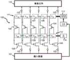
图1是可以在本发明的实施例中使用的用于分发数据的系统的示意图,其中控制平面包括单条控制链。Figure 1 is a schematic diagram of a system for distributing data that may be used in embodiments of the present invention, wherein the control plane includes a single chain of control.
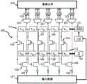
图2是可以在本发明的实施例中使用的数据分发系统的示意图,其中控制平面包括两条不同的控制链。Figure 2 is a schematic diagram of a data distribution system that can be used in embodiments of the present invention, wherein the control plane includes two distinct control chains.
图3是根据本发明的实施例的用于分发数据的系统的示意图,其中控制平面包括单条控制链,并且用于执行本地后处理计算的分布式装置被提供为本地解码器。3 is a schematic diagram of a system for distributing data according to an embodiment of the present invention, wherein the control plane includes a single chain of control and the distributed means for performing local post-processing computations are provided as local decoders.
图4解说了本发明的其中控制变量序列被编码的实施例。Figure 4 illustrates an embodiment of the present invention in which a sequence of control variables is encoded.
图5解说了如何通过同步时钟信号的分发来获得本发明的实施例的第一和第二延迟线中的延迟单元之间的成对匹配。Figure 5 illustrates how pairwise matching between delay elements in the first and second delay lines of an embodiment of the present invention is achieved by synchronizing the distribution of clock signals.
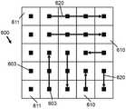
图6解说了包括像素元件的平面显示器,其中每个像素元件连接到数据输出电极,并且个体像素元件通过曲线被连接。6 illustrates a flat panel display including pixel elements, where each pixel element is connected to a data output electrode, and individual pixel elements are connected by curves.
图7解说了包括像素元件的平面显示器,其中个体像素元件通过直线被连接。7 illustrates a flat panel display including pixel elements, where individual pixel elements are connected by straight lines.
图8解说了包括像素元件的平面显示器,其中个体像素元件通过一曲线被连接,该曲线是空间填充卷绕式曲线,沿该空间填充卷绕式曲线直的曲线段通过直角转弯被连结。8 illustrates a flat panel display comprising pixel elements in which individual pixel elements are connected by a curve, which is a space-filling wrap-around curve along which straight curved segments are joined by right-angle turns.
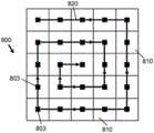
图9解说了包括像素元件的平面显示器,其中个体像素元件通过多条曲线被连接,这些曲线是空间填充卷绕式曲线,沿这些空间填充卷绕式曲线直的曲线段通过直角转弯被连结。9 illustrates a flat panel display comprising pixel elements in which individual pixel elements are connected by a plurality of curves that are space-filling wrap-around curves along which straight curved segments are connected by right-angle turns.
各附图仅是示意性而非限制性的。在附图中,出于解说性目的,可将一些要素中的尺寸放大且不按比例绘制。尺度和相对尺度并不必然对应于对本发明实践的实际简化。The figures are only schematic and non-limiting. In the drawings, the dimensions of some of the elements may be exaggerated and not drawn to scale for illustrative purposes. Dimensions and relative dimensions do not necessarily correspond to actual simplifications to the practice of the invention.
权利要求中的任何附图标记不应被解释为限制范围。Any reference signs in the claims should not be construed as limiting the scope.
在不同的附图中,相同的附图标记指代相同或相似的要素。In the different drawings, the same reference numbers refer to the same or similar elements.
具体实施方式Detailed ways
将就特定实施例并且参考某些附图来描述本发明,但是本发明不限于此,而仅由权利要求书来限定。The invention will be described in terms of specific embodiments and with reference to certain drawings, but the invention is not limited thereto, but only by the claims.
说明书中和权利要求书中的术语第一、第二等用于在类似的要素之间进行区分,而不一定用于描述时间上、空间上、等级上或以任何其他方式的顺序。应当理解,如此使用的术语在适当的情况下是可互换的并且本文中所描述的本发明实施例能够以不同于本文中所描述或解说的其他顺序操作。The terms first, second, etc. in the description and in the claims are used to distinguish between similar elements, and not necessarily to describe an order temporally, spatially, hierarchically, or in any other way. It is to be understood that the terms so used are interchangeable under appropriate circumstances and that the embodiments of the invention described herein are capable of operation in other sequences than described or illustrated herein.
此外,在说明书和权利要求书中的诸如顶部、底部、前部、后部、前缘、尾缘、下方、上方等方向性术语被用于参考正被描述的附图的取向的描述性目的,而不一定是用于描述相对位置。因为可以以数个不同的取向来放置本发明的各实施例的各组件,所以仅出于说明的目的使用方向性术语且决不作为限制,除非另有说明。因此,应当理解,如此使用的这些术语在合适情况下可以互换,并且本文所描述的本发明的各实施例能够以不同于本文所描述或解说的其他取向来操作。Furthermore, directional terms such as top, bottom, front, rear, leading edge, trailing edge, below, above, etc. in the specification and claims are used for descriptive purposes with reference to the orientation of the drawings being described , not necessarily used to describe relative positions. Since the various components of the various embodiments of the present invention may be placed in several different orientations, directional terminology is used for purposes of illustration only and in no way limiting unless otherwise stated. Therefore, it is to be understood that the terms so used are interchangeable under appropriate circumstances and that the embodiments of the invention described herein are capable of operation in other orientations than described or illustrated herein.
要注意,权利要求中使用的术语“包括”不应被解释为限定于其后列出的装置;它并不排除其他要素或步骤。因此,该术语被解释为指定所陈述的特征、整数、步骤或组件的存在,但不排除一个或多个其他特征、整数、步骤或组件、或其群组的存在或添加。因此,表述“一种包括装置A和B的设备”的范围不应当被限定于仅由组件A和B构成的设备。这意味着对于本发明,该设备的仅有的相关组件是A和B。It is to be noted that the term "comprising", used in the claims, should not be interpreted as being restricted to the means listed thereafter; it does not exclude other elements or steps. Thus, the term is to be interpreted as specifying the presence of a stated feature, integer, step or component, but not excluding the presence or addition of one or more other features, integers, steps or components, or groups thereof. Therefore, the scope of the expression "an apparatus comprising means A and B" should not be limited to apparatuses consisting of components A and B only. This means that for the present invention, the only relevant components of the device are A and B.
贯穿本说明书对“一个实施例”或“实施例”的引用意指结合该实施例所描述的特定的特征、结构或特性被包括在本发明的至少一个实施例中。因此,短语“在一个实施例中”或“在实施例中”贯穿本说明书在各个地方的出现并不一定全部指代同一实施例,而是可以指代同一实施例。此外,在一个或多个实施例中,如通过本公开将对本领域普通技术人员显而易见的,特定的特征、结构或特性能以任何合适的方式进行组合。Reference throughout this specification to "one embodiment" or "an embodiment" means that a particular feature, structure, or characteristic described in connection with the embodiment is included in at least one embodiment of the present invention. Thus, appearances of the phrases "in one embodiment" or "in an embodiment" in various places throughout this specification are not necessarily all referring to the same embodiment, but may refer to the same embodiment. Furthermore, the particular features, structures or characteristics can be combined in any suitable manner, as would be apparent to one of ordinary skill in the art from this disclosure, in one or more embodiments.
类似地,应当领会,在本发明的示例性实施例的描述中,出于精简本公开和辅助对各个发明性方面中的一个或多个发明性方面的理解的目的,本发明的各个特征有时一起被编群在单个实施例、附图或其描述中。然而,该公开方法不应被解释为反映要求保护的发明要求比每一项权利要求中明确记载的特征更多的特征的意图。相反,如所附权利要求所反映,发明性方面存在于比单个前述公开的实施例的全部特征更少的特征中。因此,具体实施方式之后所附的权利要求由此被明确纳入本具体实施方式中,其中每一项权利要求本身代表本发明的单独实施例。Similarly, it should be appreciated that in the description of the exemplary embodiments of this invention, various features of the invention are sometimes included for the purpose of streamlining the disclosure and assisting an understanding of one or more of the various inventive aspects. are grouped together in a single embodiment, figure or description thereof. However, this method of disclosure should not be interpreted as reflecting an intention that the claimed invention requires more features than are expressly recited in each claim. Rather, as the following claims reflect, inventive aspects lie in less than all features of a single foregoing disclosed embodiment. Thus, the claims following the Detailed Description are hereby expressly incorporated into this Detailed Description, with each claim standing on its own as a separate embodiment of this invention.
此外,如将由本领域技术人员所理解,尽管本文中所描述的一些实施例包括其他实施例中所包括的一些特征但不包括其他实施例中所包括的其他特征,但是不同实施例的特征的组合旨在处于本发明的范围内,并且形成不同实施例。Furthermore, as will be understood by those of ordinary skill in the art, although some embodiments described herein include some features included in other embodiments but do not include other features included in other embodiments, the features of different embodiments are Combinations are intended to be within the scope of the invention and to form different embodiments.
应当注意,在描述本发明的某些特征或方面时使用特定术语不应被当作暗示该术语在本文中被重新定义成限于包括该术语与其相关联的本发明的特征或方面的任何特定特性。It should be noted that the use of a specific term in describing certain features or aspects of the invention should not be taken as implying that the term is redefined herein to be limited to any specific characteristic including the feature or aspect of the invention with which the term is associated .
在本文中所提供的描述中,阐述了众多具体细节。然而,应当理解,可以在没有这些具体细节的情况下实践本发明的实施例。在其他实例中,公知的方法、结构和技术未被详细示出,以免混淆对本描述的理解。In the description provided herein, numerous specific details are set forth. It should be understood, however, that embodiments of the present invention may be practiced without these specific details. In other instances, well-known methods, structures and techniques have not been shown in detail in order not to obscure an understanding of this description.
定义definition
在本发明的上下文中,如在详细描述的附图和示例性实施例中所引述的控制链对应于控制平面的一部分,该部分包括引导将输入数据分发到用于修改操作地耦合到数据分发系统的显示器的像素元件的(诸)位置所必需的所有元件。因此控制链还引导这些像素元件的全部或部分更新。对输入数据的实际分发是由属于数据分发系统的数据平面的开关来执行的。控制平面可包括若干控制链,其中每条控制链被适配成用于将输入数据引导到特定的位置,并且由不同控制链寻址的位置可以交叠。In the context of the present invention, the chain of control, as referred to in the figures and exemplary embodiments of the detailed description, corresponds to the part of the control plane that includes directing the distribution of input data to operatively coupled to the distribution of data for modification All elements necessary for the location of the pixel element(s) of the display of the system. The chain of control thus also directs all or part of the updating of these pixel elements. The actual distribution of incoming data is performed by switches belonging to the data plane of the data distribution system. The control plane may include several control chains, where each control chain is adapted to direct incoming data to a specific location, and the locations addressed by different control chains may overlap.
本发明的具有数据输入电极和数据输出电极作为其相应输入和输出端子的附图和示例性实施例在后文描述。然而,技术人员将领会,本发明的实施例不限于电极,并且可以提供任何类型的适当电触点或电连接件作为输入或输出端子。Figures and exemplary embodiments of the present invention with data input electrodes and data output electrodes as their respective input and output terminals are described later. However, the skilled person will appreciate that embodiments of the present invention are not limited to electrodes and any type of suitable electrical contacts or connections may be provided as input or output terminals.
本发明的示例性实施例通常引用全息显示器/投影仪作为3D光场创建显示器或投影设备的示例;术语全息显示器和全息投影仪在它们能够观看完整3D场景的意义上可以互换使用。这不排除创建3D光场的其他显示器或投影设备落入本发明的第二方面的实施例的范围内。本领域技术人员将知道例如如何编码、格式化或组织4D光场信息流以使用(近眼)光场显示器进行投影,以使得可以使用根据本发明的第一方面的实施例的数据分发系统来分发经编码、格式化或组织的流。类似的推理也适用于具有或没有深度感知的非投影显示器中的数据分发系统,例如,适用于使用微透镜并定义宏像素以实现不均匀的角度照明和深度感知的自动立体透镜显示器。结果,在由透镜阵列增强的2D显示器的3D应用中追求经缩放、更密集且更大的像素阵列。更一般而言,还可以实践本发明以用于具有大像素密度和/或大像素计数的标准2D显示器(例如,具有数百万像素的紧凑型LCD或TFT 2D显示器,后者是无投影设备的非限制性示例,即,适合于直接观看)中的数据分发系统。此外,本发明可以被应用于其中部分动态更新是有用的并且需要能量高效的、高吞吐量、低等待时间数据分发的任何显示器。在全息投影仪的上述示例的上下文中,高吞吐量、低等待时间数据分发意味着超过10Gb/cm2的密集数据吞吐量以在亚波长范围下(例如,在四分之一波长分辨率下)的蓝光情况下也获得良好分辨率。该数据很可能以典型的帧率分发,以获得流体运动感知而没有闪烁,例如,以24fps、48fps的帧率等等。对于三色显示器,此帧率可以增至三倍。由此,对于超过1百万像素和24比特色深的典型像素计数,低等待时间数据分发系统支持超过0.5Gb/s的总数据吞吐率、以及超过1Tb/s/cm2的数据吞吐密度。相关的功耗优选地在几瓦以下的范围内,更优选地在几毫瓦以下的范围内。然而,可能没有指定整体系统性能的唯一或优选方式,并且一般而言以下规则适用:如果不能满足最大性能(速度)下的系统操作,则将引入附加的并行性以应对预期的整体系统规范。Exemplary embodiments of the present invention generally refer to a holographic display/projector as an example of a 3D light field creation display or projection device; the terms holographic display and holographic projector are used interchangeably in the sense that they are capable of viewing a full 3D scene. This does not exclude other displays or projection devices that create a 3D light field from falling within the scope of embodiments of the second aspect of the invention. Those skilled in the art will know for example how to encode, format or organize a 4D light field information stream for projection using a (near eye) light field display so that it can be distributed using a data distribution system according to an embodiment of the first aspect of the invention An encoded, formatted, or organized stream. Similar reasoning applies to data distribution systems in non-projection displays with or without depth perception, e.g. for autostereoscopic lenticular displays that use microlenses and define macropixels for uneven angular illumination and depth perception. As a result, scaled, denser and larger pixel arrays are pursued in 3D applications of 2D displays enhanced by lens arrays. More generally, the present invention can also be practiced for standard 2D displays with large pixel densities and/or large pixel counts (eg, compact LCD or TFT 2D displays with millions of pixels, the latter being non-projection devices). A non-limiting example of , i.e., a data distribution system suitable for direct viewing). Furthermore, the present invention can be applied to any display where some dynamic updates are useful and where energy efficient, high throughput, low latency data distribution is required. In the context of the above example of holographic projectors, high throughput, low latency data distribution means dense data throughput in excess of 10 Gb/cm2 at subwavelength range (eg, at quarter wavelength resolution) ) to obtain good resolution in blue light. This data is likely to be distributed at typical frame rates for fluid motion perception without flicker, eg, at 24fps, 48fps, etc. For tri-color displays, this frame rate can be tripled. Thus, for typical pixel counts in excess of 1 megapixel and 24 bit depth, the low latency data distribution system supports aggregate data throughput rates in excess of 0.5 Gb/s, and data throughput densities in excess of 1 Tb/s/cm2 . The associated power consumption is preferably in the range of a few watts or less, more preferably a few milliwatts or less. However, there may not be a unique or preferred way of specifying overall system performance, and in general the following rules apply: if system operation at maximum performance (speed) cannot be met, additional parallelism will be introduced to cope with the expected overall system specification.
现在参照图1来描述根据本发明的第一方面的实施例的用于分发数据的系统。该数据分发系统是关于全息显示器/投影仪来描述的,但不限于此,并且也可以用于其他显示器或投影仪应用中,例如,用于一般的3D光场显示器应用中,用于3D微透镜显示器中,用于具有高像素计数和/或像素密度的2D LCD显示器应用中等等。该数据分发系统可被实现为用于数据路由的多级交换网络中的最后一层,在该情形中,根据本发明的用于分发的输入数据对应于在该最后一层获得的预先路由的数据。如果是这种情形,则用于分发数据的系统的控制平面可以与通过预先路由的交换结构来引导数据路由(例如,也通过使用控制链)的控制平面重合。虽然本发明的优选实施例被描述为仅具有用于分发输入数据的单级数据开关,但是本发明不限于那些实施例。例如,可以具有用于将输入数据从起始位置分发到目标位置的两级或更多级数据开关,数据平面中的这两级或多级数据开关由控制平面很好地协调。然而,在全息显示器/投影仪应用中,多级系统的最后一层受到重要关注,因为它控制输入数据向显示器的像素元件的分发,即,它对于控制如何更新像素元件至关重要。A system for distributing data according to an embodiment of the first aspect of the present invention will now be described with reference to FIG. 1 . The data distribution system is described with respect to, but not limited to, holographic displays/projectors, and can also be used in other display or projector applications, for example, in general 3D light field display applications, for 3D micro lenticular displays, in 2D LCD display applications with high pixel count and/or pixel density, etc. The data distribution system can be implemented as the last layer in a multi-stage switching network for data routing, in which case the input data for distribution according to the invention corresponds to the pre-routed data obtained at the last layer data. If this is the case, the control plane of the system for distributing data may coincide with the control plane that directs data routing (eg, also through the use of control chains) through a pre-routed switch fabric. Although preferred embodiments of the present invention are described as having only a single stage of data switches for distributing incoming data, the present invention is not limited to those embodiments. For example, there may be two or more levels of data switches for distributing incoming data from a starting location to a destination location, the two or more levels of data switches in the data plane being well coordinated by the control plane. However, in holographic display/projector applications, the last layer of the multi-level system is of significant interest because it controls the distribution of input data to the pixel elements of the display, i.e. it is critical for controlling how the pixel elements are updated.
图1示意性地描绘了用于分发数据的系统100,该系统100包括多个数据输入电极102与多个数据输出电极103之间的多条数据路径。数据开关105(作为数据平面的一部分)沿数据路径布置以用于管理输入数据101在这些数据路径上的传输。数据输入电极102与数据输出电极103之间的数据路径可以部分地交叠,例如,开始于同一个数据输入电极102但终止于不同数据输出电极103的数据路径共享共同的区段。控制平面包括多个控制开关104以及第一和第二延迟线111、112。系统100进一步包括用于在系统运行时期间检测输入数据101流中所包含的模式的装置115。用于分发数据的系统100的数据输入电极102(例如,在多比特传输线的端部的数据输入电极)适合于当系统100在使用时(即,当输入数据110被接收并分发到显示器的可连接像素元件110以用于在像素元件110处上传和更新信号时)接收输入数据101流。该多个数据开关105中的每个数据开关连接到数据输入电极102和数据输出电极103以按受控方式将接收到的输入数据101流从数据输入电极102向数据输出电极103分发。在本发明的一些实施例中,每个数据开关105连接到恰好一个数据输入电极102和恰好一个数据输出电极103。在本发明的其他实施例中,每个数据开关105可以连接到一个数据输入电极102和若干数据输出电极103。FIG. 1 schematically depicts a
数据输出电极103可连接到显示器(例如,全息显示器)的像素元件110。至像素元件110的连接可以使得恰好一个数据输出电极103连接到一个像素元件。更一般而言,不止一个数据输出电极103可以连接到一个像素元件(例如,以并行化可以被并发地写入到像素元件的比特数、或关于每个像素元件的强度和相位水平的单独信息)。用于分发数据的系统100包括控制链,该控制链包含用于引导输入数据101从输入电极102向输出电极103的分发的元件。用于分发数据的系统100的这种控制链包括第一延迟线111和控制开关104,其中控制开关104电耦合到第一延迟线111和数据开关105。该电耦合使得如果控制开关104处于预定状态(例如,导通的开启状态(on-state))、则沿第一延迟线111传播的控制变量被选择并被导向至少一个数据开关105,藉此输入数据101从对应的数据输入电极102向对应的数据输出电极103的传输受控制。控制开关104还可操作地连接到第二延迟线112,以接收对这些控制开关104的开关事件进行控制的使能变量。如在通过援引纳入本文的EP17182232.3中更广泛描述的,第一延迟线111包括一个或多个延迟单元106、107并且与第二延迟线112处于同步关系,该第二延迟线112也包括一个或多个延迟单元108、109。这两条延迟线之间的同步关系可以通过这两条延迟线的延迟单元的成对匹配来建立。例如,第二延迟线112的延迟单元108的延迟时间τ22因变于第一延迟线111的对应延迟单元106的延迟时间τ12来确定,并且第二延迟线112的延迟单元109的延迟时间τ23因变于第一延迟线111的对应延迟单元107的延迟时间τ13来确定,等等。在本发明的一些实施例中,如下设计第一和第二延迟线的对应延迟单元可能是有利的:使得第二延迟线112的延迟单元108的延迟时间τ22在给定应用可接受的误差裕度内是第一延迟线111的对应延迟单元106的延迟时间τ12的两倍,第二延迟线112的延迟单元109的延迟时间τ23在所述误差裕度内是第一延迟线111的对应延迟单元107的延迟时间τ13的两倍,等等。第一延迟线111的延迟单元106、107与第二延迟线112的延迟单元108、109之间的这种同步关系具有如下效果:(沿第二延迟线112传播的)使能变量每次前进一个延迟单元108、109都与构成(沿第一延迟线111传播的)控制变量序列的相继控制变量在时间上对准。等效地,同步关系指出,两个序列(例如,控制变量的控制序列和使能变量的使能序列)之间的时间偏移以受控方式增加。这两个序列在第一和第二延迟线111、112上共同传播。在示例性实施例中,第二延迟线112的延迟单元108、109可以被提供为时钟控制的2比特移位寄存器,而第一延迟线111的对应延迟单元106、107可以被提供为由与第二延迟线112的2比特移位寄存器相同的时钟信号时钟控制的1比特移位寄存器。在另一示例性实施例中,延迟单元106、107、108、109可以由未由共用时钟信号同步的触发器或寄存器来提供,而其中使能变量与相继控制变量的时间对准是通过波管线输送电路系统(例如,通过将延迟缓冲器受控插入到第二延迟线112中)来实现的。在又一示例性实施例中,延迟单元106、107、108、109可以被提供为传输线分段,这些分段可以被建模并构建为集总RC电路。对传输线分段的电阻值和电容的仔细匹配导致对这两个共同传播序列之间的时间偏移的期望控制。第二延迟线112的延迟单元108、109的延迟时间不必是第一延迟线111的对应延迟单元106、107的延迟时间的恰好两倍。存在某种程度的可容忍变化性,只要能确定使能变量与相继控制变量之间的充分时间交叠即可。例如,使能变量可以被选择为存在或不存在的脉冲,并且对于控制变量同样如此。使能变量与控制变量脉冲历时相比而言较短(例如,短10%)的脉冲历时在传播期间的偏移中提供时间抖动方面的某种灵活性。因此有可能的是,第二延迟线112的延迟单元108的延迟时间τ22是第一延迟线111的对应延迟单元106的延迟时间τ12的2.1倍而不是目标值2.0,并且第二延迟线112的延迟单元109的延迟时间τ23是第一延迟线111的对应延迟单元107的延迟时间τ13的1.9倍而不是目标值2.0,等等。
在本发明的一些实施例中,第一延迟线111和第二延迟线112可以被构想成传播被表示为多个比特的控制变量或使能变量。在本发明的其他实施例中,第一延迟线111和/或第二延迟线112可被构想成传播被表示为单个比特的控制变量或使能变量。In some embodiments of the invention, the
用于提供输入数据101的装置(例如,用于将输入数据101从存储介质传输到数据分发系统(并且有可能通过预先路由网络)的数据传输装置)可被包括在数据分发系统100中或者可以在数据分发系统100外部。输入数据101可以经由有线连接或无线连接从计算机或服务器的外部存储盘传输到数据分发系统100,但不限于此。Means for providing input data 101 (eg, data transmission means for transmitting
在特定的实施例中,输入数据101被编码和/或被压缩以实现对输入数据101流的适当纠错和/或数据压缩,其获得较高的数据传输、分发和显示更新速率的优点。对于一些应用,输入投影数据101可以是离线获得的经预处理输入数据(例如,经压缩和/或经编码的输入数据)、和/或针对全息数据投影进行变换的输入数据,并且如此预处理的输入数据随后被存储在适当的存储介质(例如,计算机上的存储盘)上,当数据分发系统100操作时从该存储介质检索该数据并流送到数据分发系统100。在本发明的上下文中,输入数据101通常表示形成3D场景的代表性高级描述的预定义基元(primitive)集合中的基元。随后在本地解码和/或本地后处理步骤中解释每个基元,并在(全息)显示器的个体或各群像素元件级别得到3D场景信息的物理表示,例如,作为与显示器相互作用的光的光学相位和/或振幅分布。作为非常简单的示例,可以想象3D空间中简单的点构成整个3D场景。在(全息)显示器的个体或各群像素元件级别对该3D场景点的物理表示可对应于呈现出菲涅尔波带片的准连续或离散版本的显示器的透射调制的像素元件,或对应于模仿菲涅尔透镜轮廓的显示器的相位调制的像素元件。基元随后可以解决像素元件的整个环或其弧形部分的透射率/反射率或相位响应。In certain embodiments, the
在本发明的一些实施例中,流送的输入数据101可被拆分为输入数据101的若干较小组块,这些组块被应用于与一条以上控制链相关联的数据输入电极102。本发明的实施例的优点在于,根据本发明的实施例的数据分发系统100可以处置非常高的数据速率,例如,可以支持太比特每秒(Tbps)的数据传输速率,这对于给一名或多名观众留下连续性印象的足够高的帧率/显示器更新速率而言是必要的。通过将输入数据101分解为组块,还可以控制系统100的等待时间,以在需要时保持尽可能低的等待时间。In some embodiments of the invention, streamed
用于检测输入数据101流中所包含的模式的装置115可以接收和分析流送的输入数据101(例如,其中包含的基元或其经解释的对应物,即,其经解码表示),并且响应于此,可以向一条或多条控制链发送指令。此类指令的非限制性示例尤其是用于更新被应用并存储在数据开关105处的控制变量序列的指令,或者针对本地计算装置的、用于重复对已经分发的输入数据的后处理步骤(但使用经更新的参数)的指令。由模式检测装置115分析并检测的模式可涵盖待显示的整个3D场景或仅仅其部分的平移、旋转、以及尺度变换。对这些模式的检测是有用的,因为基元在这些模式下(例如,在平移(例如,3D场景的移动对象)或旋转(例如,3D场景的旋转对象)下)以确定性的方式改变。在这些情况下借助于本地后处理/重新计算对已传输的输入数据的修改与开始输入数据重新加载和重新分发的全新循环相比可以是更加能量高效的。虽然上述模式都意味着对输入数据101的函数变换,但也可以分析并检测动态模式。动态模式关注输入数据101分发的时间方面,例如,以何种速率更新数据输出电极103。在正常条件下,预期具有如下显示区域,这些显示区域具有要求频繁更新的快速演进的图像或场景内容,从而表示对去往对应于这些区域的数据输出电极103的输入数据101的频繁更新/覆写,而显示器的其他区域可以具有缓慢演进的图像或场景内容,并且由此要求对输入数据101的不太频繁的分发和覆写。即,该多个数据输出电极103在每个显示刷新循环仅部分地更新。因此,检测模式的装置115还可被配置成用于检测在某个时间段上输入数据101更新的准静态模式。对于这些准静态输入数据101上传模式,控制平面的控制链不经历更新动作,这实现对控制平面的更为能量高效的使用。为此目的,用于检测模式的装置可以比较检测到的供更新基元的属性的变化有多快,或者检测是否整个新基元被更新。在显示器的某个经分段、不交叠区域上检测到的稳定输入数据101上传模式通常与数据输出电极103的群集以及存储在数据开关105上的恒定控制变量序列相关联。因此,只要准静态模式持续存在(并且控制变量序列未被更新),一个群集的输入数据101的更新速率就被绑定在一起,这可以是对流送输入数据101的实际输入数据101上传速率的近似。然而,这种近似是允许的,只要在每个刷新循环中假如计及所忽略偏差的情况下这些偏差不会造成或不会严重地造成(例如,通过显著地影响图像质量)经重构3D场景的改变。The means 115 for detecting patterns contained in the stream of
最后,用于检测模式的装置115还可以检测与先前传输到特定数据输出电极103的输入数据相同的输入数据101。这同样适用于所检测到的准静态模式。在该情形中,优选地不会再次分发输入数据101以覆写旧的输入数据,并且本地后处理也是不必要的。这是通过一旦已第一次传输可重用输入数据就使相应的数据开关105保持闭合来实现的,即,相应的数据开关105(例如,高阈值电压晶体管器件)充当导通门。Finally, the
模式检测可以应用于每个数据输出电极103处的输入数据101更新事件,或者应用于数据输出电极103的群集的更新事件,该群集对应于由此寻址的连通显示器的经群集区域。输入数据101更新事件的所检测模式可以经历阈值操作,从而决定所检测模式是否应当被用作对已经分发的输入数据101的本地后处理的输入。如果未被用于发起本地后处理,则可以触发对新输入数据101的重新加载和重新分发。例如,在3D场景中的快速移动对象将需要与3D场景的缓慢旋转对象相比更频繁的输入数据101更新(例如,刷新待分发的输入数据),对于缓慢旋转对象有足够的时间来重新处理在数据输出电极103的一个或若干群集(例如,其主立体角最佳地支持场景的旋转3D对象的数据输出电极的群集)处仍然存在的已经分发的输入数据101。因此,仅在严格必要时才更新属于引导输入数据101的分发的一条或多条控制链的控制变量,以便改善能量效率。必要性标准一般取决于目标应用和/或期望的图像质量。结果,用于分发数据的系统100针对输入数据101分发的更高效方式进行动态适配。如果控制变量的一个或多个新序列变得必要(例如,响应于检测到的模式超过阈值或未检测到模式),则这些控制变量由控制平面确定并提供给第一延迟线111以供注入(或者如果涉及若干控制链则提供给多条第一延迟线)。更新相应数据开关105处的控制变量是通过同时生成使能序列(例如,行进的“1”(单个脉冲))并注入到第二延迟线112中来实现的。用于生成控制变量序列的装置113和用于生成使能变量序列的装置114可被包括在数据分发系统100的控制平面结构中,但也可以被提供为外部序列生成装置,例如,被提供为可编程比特模式生成器、FPGA、或其他计算硬件实现。Pattern detection may be applied to an
输入数据101的快速变化(对应于数据输出电极103(以及显示器的对应像素元件110)处的快速输入数据分发和更新速率)的示例是所传输的相关联数据(例如,视频数据)的完整场景变化。静态场景的前景中的移动对象或者缓慢移动和静态对象中的突然纹理变化是视频内容数据的其他非限制性示例,这些视频内容数据诱发输入数据101更新速率的变化(在没有本地后处理可用的情况下)和/或允许将全息显示表面(以及因此底层数据输出电极103)分段/群集成高输入数据101更新速率的区域(例如,由需要100帧每秒(fps)数量级的更新速率的移动对象或纹理变化触发)和中等或低输入数据101更新速率的区域(例如,由需要显著小于100fps的更新速率或完全不需要更新的静态背景或缓慢移动对象触发)。这些经群集区域可由所连接显示器的像素元件110的较大矩阵的矩形子矩阵支持,或者可由像素元件110的较大矩阵的圆形部分支持。本领域技术人员将知道其他选择是可能的。经重构3D场景中的小缺陷是可以容忍的。因此,如果3D场景被部分地修改,则一些区域可能不需要更新,例如,其主立体角支持在修改期间不变化的3D场景部分的区域。因此,可以研究输入数据101流的代表性集合(包括各种各样的视频场景和图像内容),并剖析被寻址的数据输出电极103的更新速率,如果这些数据输出电极103连接到全息显示器的其相应像素元件110,则一旦成功地分发视频场景或图像内容,这些数据输出电极103就将重建该视频场景或图像内容。这种剖析发生在数据分发系统100的设计时期间。例如,该剖析可以包括记录直方图,该直方图提供关于跨给定场景的多个数据输出电极103的更新速率的分布的信息。作为该设计时剖析(例如,通过对数据分发系统100的仿真或模拟)的结果,可以标识针对给定场景具有类似输入数据101更新速率的数据输出电极103的群集。显示平面以及由此多个底层数据输出电极103因此被划分为多个不相交群集。每个如此标识的数据输出电极103的群集可以被提供有数据分发系统100的控制平面中的单独控制链。控制链提供必要的系统基础设施以实现更新速率的变化。由于更新速率的变化对应于数据开关105的控制变量的更新,因此单条控制链提供迄今所讨论的控制平面的所有元件,即,第一和第二延迟线111、112以及多个控制开关104。然而,控制平面作为整体可以包括多条控制链,这是因为控制平面作为整体控制所标识的所有群集。如图1中所示的本发明的示例性实施例仅具有单条控制链。本发明的具有两条控制链的另一示例性实施例在图2中解说并进一步描述。本发明的各实施例的优点在于,可以标识大量群集并且向每个群集指派单独的控制链,例如,可以有100或1000、或者大于1000个群集和控制链。该大量群集提供经群集更新速率的精细粒度,从而针对相当短的控制链更新产生高图像质量和低等待时间以及每面积能量开销。An example of rapid changes in input data 101 (corresponding to fast input data distribution and update rates at data output electrodes 103 (and
对于本发明的一些实施例,包括像素元件110的显示器可连接到或可被包括在数据分发系统100中,以使得当数据分发系统100在操作时显示器的像素元件110电耦合到相应的数据输出电极103。显示器的像素元件110可被形成为包括相变材料的电可控单元,但不限于此。液晶材料、电光材料、有源受控发光二极管是电可控像素元件110的其他非限制性示例,任何特定的选择取决于显示器类型和应用。相变材料像素元件110的优点是由于以下事实:它们不需要恒定的电源来保持其当前状态;对相变材料像素元件110供电的电源可以实际上被断开,而像素元件110将记忆并保持其最后所施加的状态。因此,如果任何适当的存储器材料提供与入射在显示器上的光的足够相互作用(例如,经由衍射、反射、吸收、或其组合来改变入射光的光学相位、角度分布和/或振幅),则该材料可以被用于全息投影仪显示器的像素元件110。在本发明的优选实施例中,包括像素元件110的显示器是数据分发系统100的组成部分,例如,该显示器是在数据分发系统100被布局在其中的半导体基板的顶上形成的。例如,像素元件110被形成为单元,包括例如适当的相变材料,这些相变材料在半导体基板(例如硅基板)的顶上被沉积并图案化,该半导体基板包括用于寻址各体单元的电子控制结构并且还包括例如在垂直后端制程(BEOL)堆叠中的数据分发系统。这具有如下优点:可以获得紧凑的、完全集成的全息显示器和数据分发系统100,该系统也是晶片可处理的,由此非常适合于以降低的成本和高的可重复性进行批量制造。替换地,可以分开地提供数据分发系统100和显示器并经由适当的连接装置(诸如导线)来连接该数据分发系统和显示器。另外其他实施例可以提供在半导体基板的底表面的像素元件,例如,通过用具有电子控制结构和BEOL堆叠的TSV来连接这些像素元件。在本发明的优选实施例中,像素元件110由非常小的横向尺寸来表征,例如单个像素元件110可以在两个横向尺寸上小至100纳米或者可以甚至更小。具有减小的横向尺寸的像素元件110对于容适较大视角范围的全息显示器或其他立体显示器特别有用,例如,如果像素元件110在其横向尺寸上被设计为小于200nm(例如,被设计为在两个横向尺寸上均具有100nm),则即使在400nm蓝光的情况下也实现完整的180度视角。每个像素元件100所占据的减小的面积还允许设计更紧凑的显示器,其中每个显示器所需要的晶片管芯面积减小,这可以进一步降低制造成本。替换地,显示器的给定管芯区域可以填充有更多像素元件110,这有利于增加的显示器孔径,从而产生更佳的显示器分辨率。在本发明的优选实施例中,显示器包括至少一百万像素。For some embodiments of the invention, a display including
在本发明的一些实施例中,数据开关105和/或控制开关104可被提供为微电子晶体管器件。例如,数据开关105和/或控制开关104可以被提供为导通晶体管。这有益于由构建逻辑门所需要的晶体管(例如,导通晶体管开关)数目减小表征的数据分发系统100,因此降低了每面积能量开销、电路和路由复杂度。在本发明的一些实施例中,每个数据开关和/或每个控制开关可以对应于控制输入数据101从数据输入电极102向数据输出电极103的传输的恰好一个晶体管器件(通常为n-MOS晶体管器件)。在本发明的其他实施例中,每个数据开关和/或每个控制开关可以对应于用于控制输入数据101从数据输入电极102向数据输出电极103的传输的不止一个晶体管器件,例如,可以是但不限于完全互补n-p CMOS开关。In some embodiments of the invention, the data switch 105 and/or the
在本发明的特定实施例中,数据开关105和/或控制开关104被提供为低廉制造的薄膜晶体管(TFT)。这具有如下优点:可以使用TFT技术来垂直地堆叠被集成在BEOL工艺的金属化层之间的许多TFT层,从而实现多达十个垂直堆叠的TFT器件层或更多。因此,可以获得针对显示器的每个像素元件的减小的面积,并且同时在每像素的基础上在本地提供分布式电子像素控制逻辑和可任选的数据后处理逻辑。与常规的平面CMOS技术形成对比,由于借助穿硅通孔(TSV)在管芯堆叠之间的自上而下路由引起的每面积能量开销被避免,因此即使典型的TFT节点也可以缩放至35nm至40nm。在本发明的特定实施例中,控制开关104是高阈值电压、高阻抗器件,例如,隧穿FET或TFT器件。这具有实现低功率、低漏泄器件的优点。使用高阈值电压、高阻抗TFT器件(例如,使用铟镓锌氧化物(IGZO)材料或使用适当的2D材料(诸如石墨烯、MoS2等等)实现的TFT器件)是特别有利的。术语IGZO涵盖了化合物InxGayZnzOw就原子序数值x、y、z和w而言的所有可实现变体,例如In2Ga2ZnO。然而,本发明的实施例不限于将高阻抗特性与高阈值电压组合的器件。替换实施例可以实现仅具有高阻抗的器件或仅具有高阈值电压的器件。In certain embodiments of the invention, the data switch 105 and/or the
对于本发明的其中控制开关104被实现为高阈值电压、高阻抗TFT器件的实施例,可以实现存储在TFT器件上的电荷(例如,存储在导通栅极薄膜晶体管的栅极上的电荷)的非常低的漏泄电流。使用IGZO材料实现的单个TFT器件在可以低于2V的阈值电压下例如可以具有不高于10fA(例如,在1-10fA之间)的漏泄电流。因此,控制变量可以保留达数天或者甚至数周,而典型的CMOS器件将需要在几秒钟数量级的规则时间区间中对漏泄电荷的刷新动作,即使对于将不需要任何更新动作的静态场景或场景的静态部分亦如此。本发明的这些实施例的优点在于,控制平面不需要太频繁地更新,因为控制平面包含大多数器件。这对于实际场景更新是理想的。用户定义的后续更新值之间相似性的质量度量可以进一步限制控制平面的刷新动作,并增加期间控制变量被存储的时间区间。数据开关105优选地是具有较低阈值电压(例如,显著低于2V,例如,低于1V)的TFT器件,并且也可以使用IGZO材料来实现。如果根据本发明一些实施例,如果开关频率的增益是可观的,则作为数据开关105的TFT器件的阈值电压的降低是可接受的,例如,具有大于1MHz(例如大于10MHz)的开关频率(例如,100MHz的开关频率)的数据开关105是值得赞赏的。以较快的开关速率来操作的数据开关105也可以用于甚至更快地传输输入数据101,但是导致功耗增加。一般优选不使开关频率最大化,而是替代地在数据分发系统100中利用并行性,例如,通过提供并行操作(即,在与属于显示器的不同区域的像素元件相对应的数据输出电极103处传输和更新输入数据101)的多条链。然而,对于本发明的一些实施例,数据开关105的速度要求占主导,例如,在要求最高全息图像质量的应用中(例如,在大于约50帧每秒(fps)的输入数据101流送速率下,例如,针对三色、24fps视频质量的72fps)。对于那些情形,可以降低数据开关105的阈值电压以实现较高的开关频率。相比之下,更加能量敏感的应用要求较低的输入数据更新速率,例如,对应于约30帧每秒或更低的输入数据流送速率,并且作为交换接受一定程度较低的全息图像质量。对于这种情形,本发明的实施例可以实现高阈值数据开关105,例如,具有大于1V、大于2V、或大于5V(例如,10V)的阈值电压,这取决于诸如器件堆叠或材料选择之类的因素。作为其结果,只要连接到数据输出电极103的相关数据开关105被中断/阻止并具有低漏泄特性,所传输的投影输入数据101就将被高效地存储在该数据输出电极103上(例如,作为所存储的电荷值)。用高阈值电压CMOS器件(例如,高k氧化物CMOS)实现数据开关105例如可以使得在CMOS数据开关被关断之后电荷被存储在所连接的数据输出电极103上达若干秒。这在本发明的利用对接收到的输入数据101流中的信息的冗余或重复的重用的实施例中是有利的。实际上,如果接收到的用于传输到特定数据输出电极103或其所连接到的像素元件110的投影输入数据101与传输到该数据输出电极103或所连接到的像素元件110的先前投影输入数据101相同或足够相似,则检测这些重用/重复模式并决定将不重新传输这些数据可能是更加能量高效的。因此,在本发明的被适配成用于此类能量高效的输入数据101重用的实施例中,高阈值数据开关105确保先前传输的投影输入数据101不从特定的数据输出电极103漏泄掉。在给定典型视频投影数据集中的各帧之间的时间相关性的情况下,预期典型的输入数据101流显示出大量这些重复模式。For embodiments of the present invention in which the
在本发明的替换实施例中,可以使用平面CMOS技术来实现数据开关105和/或控制开关104的晶体管器件,并且可以借助TSV技术来垂直地堆叠有源器件管芯。这具有如下优点:非常先进的技术节点(例如,低于14nm,例如,10nm节点)可以得到非常紧凑的器件和密集逻辑。虽然图1示出了单个晶体管开关作为数据开关105和控制开关104的示例,但应理解,技术人员知道如何针对不同类型的开关(诸如许多晶体管开关,等等)进行适配。In alternative embodiments of the present invention, planar CMOS technology may be used to implement the transistor devices for
图1的用于分发数据的系统100仅包括一条控制链,但也可以包括多条链,例如,数百或数千条链。每条控制链可以不同于另一控制链,或者可以以相同方式设计一条或多条控制链。图2示意性地示出了数据分发系统200,该数据分发系统200包括用于对数据开关的开关进行控制的两条不同控制链,这两条控制链共享相同的数据输入电极102但具有不同的数据输出电极103。数据输出电极103操作地耦合到显示器(例如,全息显示器)的像素元件210。毗邻数据输出电极优选地耦合到显示表面上的相邻像素元件,但本发明的实施例不限于数据输出电极和像素元件的这种耦合方案。图2中所解说的实施例的第一控制链包括第一延迟线211和第二延迟线212,并且第二控制链也包括第一延迟线217和第二延迟线218。对于该特定实施例,第一控制链在第一和第二延迟线211、212两者中包括四对匹配的延迟单元,而第二控制链在第一和第二延迟线217、218两者中仅包括三对匹配的延迟单元。然而,本发明的实施例不限于沿控制链的第一和第二延迟线217、218的特定数目的成对延迟单元,只要沿这些延迟线传播的信号的保真度不损失,其中保真度损失程度由特定的应用确定。图2的解说性实施例还示出了被包括在数据分发系统200中的信号生成装置。信号生成装置可以进一步被划分为用于生成控制变量序列的装置213、215以及用于生成使能变量序列的装置214、216。然而,该划分不是限制性的,并且可以提供一个或多个通用信号生成装置以用于以适当的方式(例如,经由多个信号输出端口、对信号的时间复用等等)生成许多控制变量序列和/或许多使能变量序列(例如但不限于行进的‘1’)。在本发明的特定而非限制性实施例中,可以在若干控制链之中共享使能变量序列,条件是它们具有相同的效果,例如,行进的‘1’可以被注入到不止单一控制链的第二延迟线中。这有利地简化了电路设计。仍然参照图2,控制变量序列被分别注入到第一控制链的第一延迟线211和第二控制链的第一延迟线217中,而使能变量序列被分别注入到第一控制链的第二延迟线212和第二控制链的第二延迟线218中。在集成解决方案中,信号生成装置可被集成到包含数据分发系统200的相同半导体基板中,或者可以在连接到包含数据分发系统200的半导体基板的分开的管芯上提供信号生成装置。然而,本发明的实施例不限于包括信号生成装置的数据分发系统200。还可以提供数据分发系统200的延迟线而没有信号生成装置,只要当数据分发系统200在操作时延迟线可以适当地耦合到可在数据分发系统200外部的此类信号生成装置。在有利的实施例中,可以在不同的层上实现数据开关105和/或控制开关104,并且可以垂直地堆叠各层以获得数据分发系统200的紧凑或者甚至完全集成版本。参照图2,控制开关2041、2042和数据开关2051、2052例如可以在单个层(例如,包括TFT器件的第一单个层)中实现,并且控制开关2043、2044和数据开关2053、2054可以在不同的层(例如,包括TFT器件的第二单个层)中实现。这两层(例如,各自包括TFT器件的第一层和第二层)随后可以在BEOL工艺中堆叠在一起,例如,通过经由被插置在这两层之间的金属层来连接这两层。为方便起见在图2的顶部绘制显示器的像素元件210;在本发明的其中数据分发系统200在垂直BEOL层堆叠中实现的实施例中,显示器的像素元件210还可以是该堆叠的一部分,例如,可以被置于该堆叠的顶上。The
图3示意性地示出了根据本发明的实施例的数据分发系统300,其中该数据分发系统300包括单条控制链。图3中的数据分发系统类似于图1中的数据分发系统100,不同之处在于,在图3中数据分发系统300进一步被提供有用于执行本地后处理计算的装置301,藉此实现在一个或多个数据输出电极103处对所传输输入数据101的分布式后处理。本地后处理计算301的示例包括本地解码、标识出像素值与(例如,利用相变材料单元)存储在显示器上的先前值相比是否已改变、向所传输输入数据应用(几何)变换、或者检错和/或纠错。对于具有对像素值变化的标识的实施例,该比较与写入像素元件的存储器单元相比花费较少的能量。当像素值在相继更新之间几乎类似时,这可以带来显著的总能量节省。Figure 3 schematically shows a
对于图3中所示的特定实施例,用于执行本地后处理计算的装置是适合于对包含在所传输输入数据101中的经编码信息进行解码(例如,以用于解释基元)的解码器(例如,被实现为TFT电路)。在本地并以分布式方式(例如,在与单个像素或像素群/群集相对应的级别)解码所传输信息具有众多优点。具有分布式本地解码装置的数据分发系统300可以例如在较高的输入数据速率下(例如,在Tbps数量级的速率下)操作,这是因为输入数据101可以保持在高度压缩的表示中直至其被分发到目标位置,例如,被分发到与显示器的一个或多个像素元件相对应的一个或多个数据输出电极。此外,通过针对输入数据101从输入数据提供单元(例如,外部存储盘)到目标位置(例如,可连接显示器的目标像素元件,以及包括检错和纠错电路系统的本地后处理计算装置)的传输使用纠错码,在传输期间发生的错误可以在本地检测并纠正,而不会影响或减慢输入数据101至其他位置的传输。此外,提供作用于所传输输入数据101的解码器具有如下优点:与在(经解码)输入投影数据101的分发和传输之前执行解码的数据分发系统相比,减少了数据分发所需要的导线数目。导线的这种减少还节省了设计面积,并且由于总电容下降,还减少了由于导线的重复电容加载引起的每面积能量开销。在由用于执行本地后处理的分布式装置提供的额外后处理功能性与同样占据设计空间并造成每面积能量开销的本地逻辑开销之间存在折衷。技术人员将领会,可以用任何适当的器件技术(例如而不限于,TFT技术)来实现本地后处理装置。作为示例,使用铟锡锌氧化物(ITZO)材料、或使用铟镓锌氧化物(IGZO)材料、或使用适当的2D材料(诸如石墨烯、MoS2等等)实现的TFT器件可以被用于实现后处理装置。术语ITZO和IGZO分别涵盖化合物InxSnyZnzOw或InxGayZnzOw在原子序数值x、y、z和w方面的所有可实现变体,例如In2Ga2ZnO。除了TFT之外,其他器件以及甚至一体式堆叠的CMOS器件也可以是选项。作为示例而不限于此,可以使用TFT BEOL堆叠技术。然而,应领会,使用BEOL堆叠中的TFT技术的本发明实施例可以受益于如下事实:TFT器件的低漏泄电流启用导通晶体管逻辑,这通常需要逻辑门中较少的组件,并且附加地,可能不需要实现锁存器或寄存器(如在全CMOS解决方案中通常是这种情形)。在一些实施例中,经解码的所传输投影输入数据可以例如是表示在像素元件输出电压或电流范围中的用于修改像素元件的相变材料或存储器材料的固相的离散电压或电流电平的多比特电压信号。在其他实施例中,经解码的所传输投影输入数据可以是例如表示用于修改一群像素元件(例如,用于修改一起形成显示器的色彩像素的红、绿和蓝像素元件)的信息的多比特电压信号。在该情形中,显示器的像素元件被提供有适当的滤色器。For the particular embodiment shown in Figure 3, the means for performing local post-processing computations is a decoding suitable for decoding encoded information contained in the transmitted input data 101 (eg, for interpreting primitives) device (eg, implemented as a TFT circuit). Decoding the transmitted information locally and in a distributed manner (eg, at the level corresponding to a single pixel or group/cluster of pixels) has numerous advantages. The
图4解说了本发明的其中控制变量序列被编码的实施例。数据分发系统400的单条控制链类似于图1中的链,不同之处在于,第一延迟线411和第二延迟线412被适配成用于对沿第一延迟线411传播的控制变量序列中的经编码控制变量进行解码。用于生成经编码控制变量序列的装置413操作地连接到链的至少第一延迟线411,并且在一些实施例中可以被包括在数据分发系统400中。一个或多个解码器401经由相应的控制开关连接到第一延迟线411。因此,单个经编码控制变量(例如,经编码控制比特)可以由控制开关从沿第一延迟线411的位置选择,该控制开关在该时刻从第二延迟线412接收到使能变量,藉此该控制开关被开启。该单个经解码控制变量被定向到解码器401,结果是该单个经解码控制变量被解码成一组经解码控制变量,这些经解码控制变量被发送到用于控制输入数据101的传输的对应一组数据开关。Figure 4 illustrates an embodiment of the present invention in which a sequence of control variables is encoded. The single control chain of the
图5解说了延迟线511、512,其中延迟线511、512的成对匹配的延迟单元具有处于同步关系的延迟时间。对于该特定实施例,延迟时间的同步是通过同步时钟信号的分发来获得的。时钟信号生成装置501可以被包括在数据分发系统中或者可以被提供为外部单元。由时钟信号生成装置501生成的同步时钟信号被分发到第一延迟线511的延迟单元和第二延迟线512的延迟单元。根据该实施例,延迟线511、512可以包括时钟控制的移位寄存器作为延迟单元506、507、509和509。寄存器被适配成用于在所施加的时钟信号经历规定的转变的情况下对这些寄存器输入处呈现的序列(例如,由其相应装置(例如,信号源513、514)生成的控制变量序列和使能变量序列)执行移位操作。在本发明的一些实施例中,链的第二延迟线的延迟单元的延迟时间在可接受的误差裕度内是第一延迟线的对应延迟单元的延迟时间的两倍。对于图5的示例性实施例,这可以通过以下操作获得:在双边沿时钟信号的上升沿和下降沿两者上(即,规则周期性时钟信号的每半个循环)触发第一延迟线511的延迟单元506、507,而第二延迟线512的对应延迟单元508、509在整个时钟循环中仅被触发一次(例如,仅在时钟信号的下降沿上触发)。替换地,如果控制变量序列和使能变量序列是比特序列,则第一延迟线511的延迟单元506、507可以是n比特移位寄存器(例如,1比特寄存器),而第二延迟线512的对应延迟单元508、509可以是2n比特移位寄存器(例如,2比特移位寄存器)。如先前实施例中所描述的,所选择的通过控制开关104的控制变量被定向到用于控制输入数据101的传输的数据开关。通过的控制变量可以被高效地存储(低漏泄电流)为可以被用于实现数据开关的晶体管器件(例如,TFT器件)的栅极电容器上的电荷。使用同步移位寄存器实现的延迟线具有如下优点:它们允许对应延迟单元的延迟时间的非常精确同步。此外,移位寄存器可以被用于恢复经移位的序列变量的信号电平,从而实现针对沿这些延迟线传播的信号的更佳信号保真度,例如,由于信号衰减引起的信号保真度损失被限制。另一优点在于以下事实:移位寄存器(例如,CMOS移位寄存器)可以在每次注入和传播循环之后完全关断,从而在延迟线空闲时降低静态功耗。FIG. 5 illustrates
在第二方面,本发明涉及一种包括第一方面的数据分发系统的3D光场投影设备(例如,全息显示器)。该3D光场投影设备还包括具有像素元件的显示器,其中像素元件耦合到数据分发系统的数据输出电极。多个像素元件被布置在显示表面上,该显示表面优选地是平面表面。然而,对于涉及投影设备的一些实施例,将该多个像素元件布置在柔性基板上可能是有用的。这具有如下优点:显示器可以被安装或可移除地附连到不均匀的非平面支撑结构,并且还承受较高的弯曲应力。显示器和显示器的像素元件可以共享关于与本发明的第一方面相关的先前实施例(具体而言,关于与图1相关的描述)已经描述的一些或所有属性。例如,在投影设备的优选实施例中,像素元件包括具有记忆功能的相变材料,即,像素元件保持在最后施加的信号使该像素元件处于的状态中,即使在不再提供任何激励信号的情形中。显示器的像素元件可以被编群在一起。在一些实施例中,使毗邻像素元件编群在一起以实现色彩像素可能是有利的,例如,通过向像素元件应用色彩掩模或滤色器以使得红、绿和蓝像素元件在显示表面上是相邻像素元件。In a second aspect, the present invention relates to a 3D light field projection device (eg, a holographic display) comprising the data distribution system of the first aspect. The 3D light field projection apparatus also includes a display having pixel elements, wherein the pixel elements are coupled to data output electrodes of the data distribution system. A plurality of pixel elements are arranged on a display surface, which is preferably a planar surface. However, for some embodiments involving projection devices, it may be useful to arrange the plurality of pixel elements on a flexible substrate. This has the advantage that the display can be mounted or removably attached to uneven, non-planar support structures, and is also subjected to high bending stresses. The display and the pixel elements of the display may share some or all of the properties that have been described with respect to previous embodiments in relation to the first aspect of the invention, in particular with respect to the description in relation to FIG. 1 . For example, in a preferred embodiment of the projection device, the pixel element comprises a phase-change material with a memory function, ie the pixel element remains in the state that the last applied signal left the pixel element in, even when no excitation signal is provided anymore. in the situation. The pixel elements of a display can be grouped together. In some embodiments, it may be advantageous to group adjacent pixel elements together to achieve color pixels, for example, by applying a color mask or color filter to the pixel elements so that red, green, and blue pixel elements are on the display surface are adjacent pixel elements.
对于投影设备的一些实施例,数据分发系统可以被优化成与特定的显示器或显示器的特定区域一起工作,如后文更详细解释的。For some embodiments of the projection apparatus, the data distribution system may be optimized to work with a specific display or a specific area of a display, as explained in more detail below.
图6解说了包括像素元件610的平面显示器600,其中每个像素元件610连接到数据输出电极603。如先前解释的,在控制链的数据开关处对控制变量的更新优选地是依次的、有时间顺序的过程(波管线输送),并且连续地更新控制变量的数据开关可以相应地被排序。波管线输送过程引起最高输入数据吞吐量和最少的面积/能量开销。然而,对控制平面的控制链进行控制的外部主机(例如,PC)必须离线或预先计算要应用哪些控制序列和使能序列以协调一切。该离线阶段(其可以是非常复杂的软件工具)将确保(例如,来自外部存储设备的)输入数据的馈送以与控制平面的控制链的馈送同步的方式发生。在波管线输送情形中,该协调变得极其复杂,因此离线阶段变得昂贵。替换地,可以阻止该离线计算并推送至在线阶段。在此类实现中,首先加载用于控制数据开关的所有控制链的新控制变量,并且随后才将输入数据分发到经更新的数据路径上。直至所有新控制变量都存在的时刻,对于经加载输入数据的分发有两种选项。输入数据要么在没有中断的情况下被加载并分发到先前指派的数据路径上(因为新数据路径还未完全更新),要么强制停顿以加载新输入数据。前一选项需要额外的电路系统来存储旧控制变量(例如,在TFT导通晶体管后面),并且随后一次更新所有旧控制变量(例如,使用额外的外部控制比特)。后一选项意味着旧像素值(对应于先前路由到该像素元件的输入数据)被暂时保持在显示器上。给定发生该控制变量加载的非常高的速率(10-100MHz),这可能不是问题,因为像素元件所连接到的数据输出电极的更新速率不需要高于100Hz。FIG. 6 illustrates a
由于每个数据开关实现将输入数据传输到特定的数据输出电极、并且由此传输到该数据输出电极所连接到的显示器的特定像素元件或像素元件群,因此由控制链的控制序列驱动的数据开关的排序自然导致所寻址像素元件或像素元件群在显示表面上的排序。按此次序连接所寻址像素元件的几何中心得到被限定并限制于显示表面的曲线。所寻址的像素元件群由此被视为仅由曲线上的一个点表示的块像素或宏像素实体。结果,数据输出电极的每个群集和所连接的像素元件被提供有至少一条控制链。通常将提供每群集一条控制链,但如果控制链变得太长(例如,在更新像素元件的等待时间方面),则需要将其分解为多条控制链。与群集相关联的(诸)控制链控制该群集中像素元件的更新速率,并且该群集中的更新速率的改变是沿着连接该群集的(块)像素元件的曲线依次执行的。因此,还可以设计特定的链,以使得它们在群集内呈现出期望的更新次序形状(精细粒度)。Since each data switch implements the transfer of input data to a specific data output electrode, and thus to a specific pixel element or group of pixel elements of the display to which the data output electrode is connected, the data driven by the control sequence of the control chain The ordering of the switches naturally results in the ordering of the addressed pixel elements or groups of pixel elements on the display surface. Connecting the geometric centers of the addressed pixel elements in this order results in a curve that is defined and confined to the display surface. The addressed group of pixel elements is thus regarded as a block pixel or macro pixel entity represented by only a point on the curve. As a result, each cluster of data output electrodes and connected pixel elements is provided with at least one control chain. Typically one chain of control per cluster will be provided, but if the chain of control becomes too long (eg in terms of latency to update pixel elements) it will need to be broken up into multiple chains of control. The control chain(s) associated with the cluster control the update rate of the pixel elements in the cluster, and changes in the update rate in the cluster are performed sequentially along a curve connecting the (blocks) of pixel elements of the cluster. Therefore, specific chains can also be designed such that they exhibit the desired update order shape (fine grain) within the cluster.
对于本发明的一些实施例,控制变量和使能变量的序列在系统设计时期间被预先计算(离线计算),例如,在系统使用期间创建并使用有限的指令序列集。对于本发明的其他实施例,控制变量和使能变量的序列是在系统运行时生成的,其益处是实现更大的灵活性并且不必在设计时再构建完全预定义的指令集。基于设计时剖析,将最可能出现的输入数据集(流)及其对应的控制和使能变量序列进行编群的一组适当的运行时种子场景被确定,以使得其粒度(定义更新序列的“形状”)远小于由控制平面在系统运行时期间所使用的控制和使能变量序列的最终粒度大小。在运行时,从可能出现输入数据集的可用种子场景开始,可以形成可用种子场景的组合,以使得将形成较大的复合“可能”输入数据集和相关的控制/使能变量序列,并因此将分别覆盖2D或3D全息换能器的较大表面或体积。这可以通过运行时决策引擎来实现,该决策引擎探索最有前途的复合物,并在此基础上执行控制平面的控制/使能变量序列和数据平面的“可能”数据集的最终实现。这意味着流送的输入数据通过种子场景数据集的组合来近似。附加地,本发明的特定实施例还可以决定设计时规则/条件,这些规则/条件管控基元种子场景群集可以被组合成复合物的方式,藉此在运行时必须花费的探索工作量和时间进一步被限制。For some embodiments of the invention, the sequences of control variables and enable variables are precomputed (offline computation) during system design time, eg, a limited set of instruction sequences is created and used during system use. For other embodiments of the invention, the sequences of control and enable variables are generated at system runtime, with the benefit of enabling greater flexibility and not having to build a fully pre-defined instruction set at design time. Based on design-time profiling, a suitable set of run-time seed scenarios that group the most likely input datasets (streams) and their corresponding sequences of control and enabling variables are determined such that their granularity (defining the sequence of updates "shape") is much smaller than the final granularity size of the sequence of control and enabling variables used by the control plane during system runtime. At runtime, starting from the available seed scenarios where the input dataset may appear, a combination of available seed scenarios can be formed such that a larger composite "possible" input dataset and associated sequence of control/enable variables will be formed, and thus Larger surfaces or volumes of 2D or 3D holographic transducers, respectively, will be covered. This can be achieved by a runtime decision engine that explores the most promising complexes, and on that basis performs the final realization of the sequence of control/enable variables for the control plane and the "possible" dataset for the data plane. This means that the streamed input data is approximated by a combination of seed scene datasets. Additionally, certain embodiments of the present invention may also determine design-time rules/conditions that govern the manner in which clusters of primitive seed scenes may be combined into composites, whereby the amount of exploration effort and time that must be spent at runtime further restricted.
在本发明的一些实施例中,多条控制链由此对应于多条此类曲线,并且优选地但不限于此,这些曲线在显示表面上不相交。这意味着这些曲线不会跨越自身,也不会跨越显示表面上的其他曲线。然而,技术人员将领会,不相交曲线不限制本发明的实施例,这是因为已知的3D BEOL堆栈技术还允许在对于期望应用而言恰适的情况下设计相交曲线。在相同或其他实施例中,此类曲线连接显示表面上的相邻(块)像素元件。此处,相邻(块)像素元件是指最接近的(块)像素元件。因此,在图6中示出了示例,其中显示表面上的多条曲线对应于多条直线620,并且没有任何两条此类直线相交。直线620可以不同地取向并且可以具有不同长度。显示器600也可以包括不经受部分更新、甚至可能未被主动用于投影的其他像素元件611,并且因此,针对这种像素元件611未规定曲线。技术人员将领会,并非显示器的所有像素元件都有助于3D光场的创建。一些像素元件可以被显示器面板隐藏,或者可以用于不同的目的,例如,用于显示器反馈、显示器校准、感官测量等等。在图6中,一列像素元件611是用于显示器校准的像素元件的示例性布置,但是其他布置也是可能的,并且不限于特定的行或列。In some embodiments of the invention, the plurality of control chains thus correspond to a plurality of such curves, and preferably, but not limited thereto, the curves do not intersect on the display surface. This means that these curves do not span themselves or other curves on the display surface. However, the skilled person will appreciate that disjoint curves do not limit embodiments of the present invention, as known 3D BEOL stacking techniques also allow intersecting curves to be designed where appropriate for the desired application. In the same or other embodiments, such curves connect adjacent (block) pixel elements on the display surface. Here, adjacent (block) pixel elements refer to the closest (block) pixel elements. Thus, an example is shown in FIG. 6 where the plurality of curves on the display surface correspond to the plurality of
图7示出了包括像素元件710的平面显示器700,其中每个像素元件耦合到对应的数据输出电极703,并且多条像素连接曲线720被成形为显示表面上的一组平行直线。对于该特定实施例,每条曲线、并且因此每一底层控制链对应于显示器700的一行像素元件。这种配置的几何形状特别简单,这促成底层电路设计和针对路由的平面规划。7 shows a
图8示出了包括像素元件810的平面显示器800,其中每个像素元件耦合到对应的数据输出电极803,并且单条像素连接曲线820被成形为空间填充卷绕式曲线,沿该空间填充卷绕式曲线直的曲线段通过直角转弯被连结,在该情形中为直角向内螺旋蛇形曲线。Figure 8 shows a
图9示出了包括像素元件910的平面显示器900,其中每个像素元件耦合到对应的数据输出电极903,并且许多像素连接曲线920被成形为空间填充卷绕式曲线,沿该空间填充卷绕式曲线直的曲线段通过直角转弯被连结。该组空间填充卷绕式曲线920形成像素元件的不相交群集,并且它们的并集覆盖整个显示器900。9 shows a
尽管在附图和前述描述中已经详细地解说和描述了本发明,但此类解说和描述应被认为是解说性或示例性的而非限制性的。前述描述详细说明了本发明的某些实施例。然而,应当领会,不论前述描述在文本中显得如何详细,本发明能以许多方式来实施。本发明不限于所公开的实施例。While the invention has been illustrated and described in detail in the drawings and foregoing description, such illustration and description are to be considered illustrative or exemplary and not restrictive. The foregoing description details certain embodiments of the present invention. It should be appreciated, however, that no matter how detailed the foregoing description appears in the text, the invention can be embodied in many ways. The invention is not limited to the disclosed embodiments.
在实施所要求保护的发明时,所公开的实施例的其他变型可以由本领域技术人员从对附图、本公开以及所附权利要求的研究而理解和实现。在权利要求中,词语“包括”不排除其他元件或步骤,并且不定冠词“一”或“一个”(“a”或“an”)不排除复数。在相互不同的从属权利要求中记载某些措施的纯粹事实并不指示不能有利地使用这些措施的组合。权利要求中的任何附图标记不应被解释为限制范围。Other variations to the disclosed embodiments can be understood and effected by those skilled in the art in practicing the claimed invention, from a study of the drawings, this disclosure, and the appended claims. In the claims, the word "comprising" does not exclude other elements or steps, and the indefinite article "a" or "an" ("a" or "an") does not exclude a plural. The mere fact that certain measures are recited in mutually different dependent claims does not indicate that a combination of these measures cannot be used to advantage. Any reference signs in the claims should not be construed as limiting the scope.
Claims (15)
Applications Claiming Priority (3)
| Application Number | Priority Date | Filing Date | Title |
|---|---|---|---|
| EP18176173.5 | 2018-06-05 | ||
| EP18176173.5AEP3579219B1 (en) | 2018-06-05 | 2018-06-05 | Data distribution for holographic projection |
| PCT/EP2019/064374WO2019233959A1 (en) | 2018-06-05 | 2019-06-03 | Data distribution for holographic projection |
Publications (2)
| Publication Number | Publication Date |
|---|---|
| CN112119447Atrue CN112119447A (en) | 2020-12-22 |
| CN112119447B CN112119447B (en) | 2023-12-12 |
Family
ID=62712739
Family Applications (1)
| Application Number | Title | Priority Date | Filing Date |
|---|---|---|---|
| CN201980032531.XAActiveCN112119447B (en) | 2018-06-05 | 2019-06-03 | Data distribution for holographic projection |
Country Status (6)
| Country | Link |
|---|---|
| US (1) | US11847944B2 (en) |
| EP (1) | EP3579219B1 (en) |
| JP (1) | JP7509696B2 (en) |
| KR (1) | KR102630929B1 (en) |
| CN (1) | CN112119447B (en) |
| WO (1) | WO2019233959A1 (en) |
Cited By (2)
| Publication number | Priority date | Publication date | Assignee | Title |
|---|---|---|---|---|
| CN113920929A (en)* | 2021-11-12 | 2022-01-11 | 深圳市迈普视通科技有限公司 | Display screen bit depth expansion device and method and LED display screen |
| CN115209212A (en)* | 2021-04-13 | 2022-10-18 | 北京小米移动软件有限公司 | System chip, electronic equipment and screen projection method of electronic equipment |
Families Citing this family (2)
| Publication number | Priority date | Publication date | Assignee | Title |
|---|---|---|---|---|
| WO2022064679A1 (en)* | 2020-09-28 | 2022-03-31 | 日本電気株式会社 | Prediction device, prediction method, and recording medium |
| KR20230060767A (en)* | 2021-10-28 | 2023-05-08 | 주식회사 엘엑스세미콘 | Display processor ans method for processing image data for driving display panel |
Citations (26)
| Publication number | Priority date | Publication date | Assignee | Title |
|---|---|---|---|---|
| US4967375A (en)* | 1986-03-17 | 1990-10-30 | Star Technologies, Inc. | Fast architecture for graphics processor |
| US4980853A (en)* | 1988-03-04 | 1990-12-25 | Chips And Technologies, Inc. | Bit blitter with narrow shift register |
| US20030160753A1 (en)* | 2002-02-11 | 2003-08-28 | Mccartney Richard I. | Display line drivers and method for signal propagation delay compensation |
| US20050057479A1 (en)* | 2003-08-25 | 2005-03-17 | Richards Peter W. | Deinterleaving transpose circuits in digital display systems |
| US20060277399A1 (en)* | 2005-06-01 | 2006-12-07 | Renesas Technology Corp. | Semiconductor device and data processing system |
| CN1979274A (en)* | 2005-12-05 | 2007-06-13 | 三星电子株式会社 | Liquid crystal display and driving method thereof |
| US7237055B1 (en)* | 2003-10-22 | 2007-06-26 | Stretch, Inc. | System, apparatus and method for data path routing configurable to perform dynamic bit permutations |
| US20080189751A1 (en)* | 2007-02-07 | 2008-08-07 | Weaver Timothy H | Methods & Systems for image processing |
| US20090051759A1 (en)* | 2005-05-27 | 2009-02-26 | Adkins Sean M | Equipment and methods for the synchronization of stereoscopic projection displays |
| US20100194857A1 (en)* | 2009-02-03 | 2010-08-05 | Bit Cauldron Corporation | Method of stereoscopic 3d viewing using wireless or multiple protocol capable shutter glasses |
| CN101802725A (en)* | 2007-05-16 | 2010-08-11 | 视瑞尔技术公司 | Holographic display |
| CN101842752A (en)* | 2007-11-02 | 2010-09-22 | 蓝光光学有限公司 | Holographic image display system |
| US20100309179A1 (en)* | 2008-01-21 | 2010-12-09 | Seereal Technologies S.A. | Device for Controlling Pixels and Electronic Display Unit |
| CN102654697A (en)* | 2012-04-25 | 2012-09-05 | 北京京东方光电科技有限公司 | Holographic liquid crystal display (LCD), stereo display method and stereo display system |
| CN103000141A (en)* | 2010-02-02 | 2013-03-27 | 皮克斯特罗尼克斯公司 | Circuits for controlling display apparatus |
| US20130100181A1 (en)* | 2011-10-20 | 2013-04-25 | Wooyoung Choe | Digital hologram image reproducing device and synchronization control method thereof |
| CN103947116A (en)* | 2011-11-16 | 2014-07-23 | 高通股份有限公司 | Apparatus and method for recovering burst-mode pulse width modulation (PWM) and non-return-to-zero (NRZ) data |
| CN104335270A (en)* | 2012-05-23 | 2015-02-04 | 伊格尼斯创新公司 | Display systems with compensation for line propagation delay |
| CN104933942A (en)* | 2015-01-22 | 2015-09-23 | 中国石油技术开发公司 | Ring screen projection system of land drilling rig installation operation simulation system, and image processing method thereof |
| CN105629488A (en)* | 2016-03-10 | 2016-06-01 | 上海工程技术大学 | Holographic imaging KTV system |
| US20160284297A1 (en)* | 2015-03-26 | 2016-09-29 | Novatek Microelectronics Corp. | Source driver apparatus and operating method thereof |
| CN106463160A (en)* | 2014-04-30 | 2017-02-22 | 高通股份有限公司 | Variable Read Latency System |
| CN106663078A (en)* | 2014-09-04 | 2017-05-10 | 高通股份有限公司 | Delay circuits and related systems and methods |
| CN106707680A (en)* | 2017-03-10 | 2017-05-24 | 东南大学 | Holographic projection method based on light field |
| CN106937531A (en)* | 2014-06-14 | 2017-07-07 | 奇跃公司 | Method and system for generating virtual and augmented reality |
| CN107077186A (en)* | 2014-07-30 | 2017-08-18 | 线性代数技术有限公司 | Low Power Computational Imaging |
Family Cites Families (19)
| Publication number | Priority date | Publication date | Assignee | Title |
|---|---|---|---|---|
| US4899307A (en)* | 1987-04-10 | 1990-02-06 | Tandem Computers Incorporated | Stack with unary encoded stack pointer |
| US5142494A (en)* | 1990-02-26 | 1992-08-25 | Eastman Kodak Company | Memory based line-delay architecture |
| US5901092A (en)* | 1997-08-22 | 1999-05-04 | Micron Technology, Inc. | Memory device having pipelined access and method for pipelining data access |
| CN1186677C (en)* | 2000-03-30 | 2005-01-26 | 精工爱普生株式会社 | Display |
| JP3744826B2 (en)* | 2001-06-04 | 2006-02-15 | セイコーエプソン株式会社 | Display control circuit, electro-optical device, display device, and display control method |
| JP4923343B2 (en)* | 2001-07-12 | 2012-04-25 | ソニー株式会社 | Display device and portable terminal equipped with the same |
| JP2004134974A (en)* | 2002-10-09 | 2004-04-30 | Amtran Technology Co Ltd | Method and apparatus for adjusting horizontal synchronizing signal and vertical synchronizing signal of display unit |
| TWI354254B (en)* | 2006-09-22 | 2011-12-11 | Chimei Innolux Corp | Liquid crystal panel and driving circuit of the sa |
| US20080238895A1 (en)* | 2007-03-29 | 2008-10-02 | Jin-Ho Lin | Driving Device of Display Device and Related Method |
| JP5457286B2 (en)* | 2010-06-23 | 2014-04-02 | シャープ株式会社 | Drive circuit, liquid crystal display device, and electronic information device |
| JP2013120981A (en)* | 2011-12-06 | 2013-06-17 | Renesas Electronics Corp | Data driver, display panel drive device and display device |
| US8996430B2 (en)* | 2012-01-27 | 2015-03-31 | International Business Machines Corporation | Hierarchical scalable neuromorphic synaptronic system for synaptic and structural plasticity |
| US9905159B2 (en)* | 2012-11-01 | 2018-02-27 | Imec Vzw | Digital driving of active matrix displays |
| JP6563267B2 (en)* | 2015-07-10 | 2019-08-21 | ラピスセミコンダクタ株式会社 | Display device driver |
| EP3472827B1 (en)* | 2016-10-27 | 2021-12-01 | Dualitas Ltd. | Method of operating a display driver |
| EP3432226B1 (en)* | 2017-07-19 | 2023-11-01 | IMEC vzw | Control plane organisation for flexible digital data plane |
| CN107945748B (en)* | 2017-12-12 | 2020-06-23 | 京东方科技集团股份有限公司 | A backlight driving device, method, backlight module and display device |
| KR102862407B1 (en)* | 2020-08-10 | 2025-09-23 | 삼성디스플레이 주식회사 | Display device |
| US11232824B1 (en)* | 2020-12-11 | 2022-01-25 | International Business Machines Corporation | Non-volatile analog resistive memory cells implementing ferroelectric select transistors |
- 2018
- 2018-06-05EPEP18176173.5Apatent/EP3579219B1/enactiveActive
- 2019
- 2019-06-03JPJP2020567593Apatent/JP7509696B2/enactiveActive
- 2019-06-03KRKR1020207030096Apatent/KR102630929B1/enactiveActive
- 2019-06-03USUS16/972,838patent/US11847944B2/enactiveActive
- 2019-06-03WOPCT/EP2019/064374patent/WO2019233959A1/ennot_activeCeased
- 2019-06-03CNCN201980032531.XApatent/CN112119447B/enactiveActive
Patent Citations (26)
| Publication number | Priority date | Publication date | Assignee | Title |
|---|---|---|---|---|
| US4967375A (en)* | 1986-03-17 | 1990-10-30 | Star Technologies, Inc. | Fast architecture for graphics processor |
| US4980853A (en)* | 1988-03-04 | 1990-12-25 | Chips And Technologies, Inc. | Bit blitter with narrow shift register |
| US20030160753A1 (en)* | 2002-02-11 | 2003-08-28 | Mccartney Richard I. | Display line drivers and method for signal propagation delay compensation |
| US20050057479A1 (en)* | 2003-08-25 | 2005-03-17 | Richards Peter W. | Deinterleaving transpose circuits in digital display systems |
| US7237055B1 (en)* | 2003-10-22 | 2007-06-26 | Stretch, Inc. | System, apparatus and method for data path routing configurable to perform dynamic bit permutations |
| US20090051759A1 (en)* | 2005-05-27 | 2009-02-26 | Adkins Sean M | Equipment and methods for the synchronization of stereoscopic projection displays |
| US20060277399A1 (en)* | 2005-06-01 | 2006-12-07 | Renesas Technology Corp. | Semiconductor device and data processing system |
| CN1979274A (en)* | 2005-12-05 | 2007-06-13 | 三星电子株式会社 | Liquid crystal display and driving method thereof |
| US20080189751A1 (en)* | 2007-02-07 | 2008-08-07 | Weaver Timothy H | Methods & Systems for image processing |
| CN101802725A (en)* | 2007-05-16 | 2010-08-11 | 视瑞尔技术公司 | Holographic display |
| CN101842752A (en)* | 2007-11-02 | 2010-09-22 | 蓝光光学有限公司 | Holographic image display system |
| US20100309179A1 (en)* | 2008-01-21 | 2010-12-09 | Seereal Technologies S.A. | Device for Controlling Pixels and Electronic Display Unit |
| US20100194857A1 (en)* | 2009-02-03 | 2010-08-05 | Bit Cauldron Corporation | Method of stereoscopic 3d viewing using wireless or multiple protocol capable shutter glasses |
| CN103000141A (en)* | 2010-02-02 | 2013-03-27 | 皮克斯特罗尼克斯公司 | Circuits for controlling display apparatus |
| US20130100181A1 (en)* | 2011-10-20 | 2013-04-25 | Wooyoung Choe | Digital hologram image reproducing device and synchronization control method thereof |
| CN103947116A (en)* | 2011-11-16 | 2014-07-23 | 高通股份有限公司 | Apparatus and method for recovering burst-mode pulse width modulation (PWM) and non-return-to-zero (NRZ) data |
| CN102654697A (en)* | 2012-04-25 | 2012-09-05 | 北京京东方光电科技有限公司 | Holographic liquid crystal display (LCD), stereo display method and stereo display system |
| CN104335270A (en)* | 2012-05-23 | 2015-02-04 | 伊格尼斯创新公司 | Display systems with compensation for line propagation delay |
| CN106463160A (en)* | 2014-04-30 | 2017-02-22 | 高通股份有限公司 | Variable Read Latency System |
| CN106937531A (en)* | 2014-06-14 | 2017-07-07 | 奇跃公司 | Method and system for generating virtual and augmented reality |
| CN107077186A (en)* | 2014-07-30 | 2017-08-18 | 线性代数技术有限公司 | Low Power Computational Imaging |
| CN106663078A (en)* | 2014-09-04 | 2017-05-10 | 高通股份有限公司 | Delay circuits and related systems and methods |
| CN104933942A (en)* | 2015-01-22 | 2015-09-23 | 中国石油技术开发公司 | Ring screen projection system of land drilling rig installation operation simulation system, and image processing method thereof |
| US20160284297A1 (en)* | 2015-03-26 | 2016-09-29 | Novatek Microelectronics Corp. | Source driver apparatus and operating method thereof |
| CN105629488A (en)* | 2016-03-10 | 2016-06-01 | 上海工程技术大学 | Holographic imaging KTV system |
| CN106707680A (en)* | 2017-03-10 | 2017-05-24 | 东南大学 | Holographic projection method based on light field |
Cited By (2)
| Publication number | Priority date | Publication date | Assignee | Title |
|---|---|---|---|---|
| CN115209212A (en)* | 2021-04-13 | 2022-10-18 | 北京小米移动软件有限公司 | System chip, electronic equipment and screen projection method of electronic equipment |
| CN113920929A (en)* | 2021-11-12 | 2022-01-11 | 深圳市迈普视通科技有限公司 | Display screen bit depth expansion device and method and LED display screen |
Also Published As
| Publication number | Publication date |
|---|---|
| US11847944B2 (en) | 2023-12-19 |
| KR102630929B1 (en) | 2024-01-30 |
| JP7509696B2 (en) | 2024-07-02 |
| EP3579219B1 (en) | 2022-03-16 |
| CN112119447B (en) | 2023-12-12 |
| JP2021527233A (en) | 2021-10-11 |
| EP3579219A1 (en) | 2019-12-11 |
| KR20210018197A (en) | 2021-02-17 |
| US20210247720A1 (en) | 2021-08-12 |
| WO2019233959A1 (en) | 2019-12-12 |
Similar Documents
| Publication | Publication Date | Title |
|---|---|---|
| CN112119447B (en) | Data distribution for holographic projection | |
| US10387303B2 (en) | Non-volatile storage system with compute engine to accelerate big data applications | |
| TWI611386B (en) | Display driving device, display apparatus and method for operating the same | |
| TWI514362B (en) | Shift register module and method for driving the same | |
| JP2022530779A (en) | Systems and methods for loss image and video compression and / or transmission utilizing meta-networks or neural networks | |
| US8989509B2 (en) | Streaming wavelet transform | |
| EP3382565A1 (en) | Selective noise tolerance modes of operation in a memory | |
| US7818464B2 (en) | Apparatus and method for capturing serial input data | |
| US12254933B2 (en) | Smart prologue for nonvolatile memory program operation | |
| US12197362B2 (en) | Batch matrix multiplication operations in a machine learning accelerator | |
| CN114783360A (en) | Grid driving control method and system, display driving system and display device | |
| EP3686874B1 (en) | Display system with variable resolution | |
| CN105721848A (en) | Method of displaying a stereoscopic image and display device | |
| JPWO2019233959A5 (en) | ||
| CN105843981A (en) | Circuit design system and semiconductor circuit designed using the system | |
| JP2012043198A (en) | Semiconductor integrated circuit | |
| US12242854B2 (en) | Compressing instructions for machine-learning accelerators | |
| Dong et al. | A 1920× 1080 129fps 4.3 pJ/pixel stereo-matching processor for pico aerial vehicles | |
| KR102105644B1 (en) | Apparatus for Storing Images in MLC STT-MRAM and Method Thereof | |
| US20150379679A1 (en) | Single Read Composer with Outputs | |
| CN116114008A (en) | Apparatus and method for refresh process when displaying images on LED panel | |
| US20250245285A1 (en) | Near memory processing device for processing hierarchical commands to process coefficient elements resulting from decomposition of polynomials | |
| Suzuki et al. | Method of downsizing the 4K uncompressed video signal generator | |
| WO2025157615A1 (en) | Near memory processing device for processing coefficient elements resulting from decomposition of polynomials | |
| Chou | Design Techniques for Energy-Efficient and Scalable Machine Learning Accelerators |
Legal Events
| Date | Code | Title | Description |
|---|---|---|---|
| PB01 | Publication | ||
| PB01 | Publication | ||
| SE01 | Entry into force of request for substantive examination | ||
| SE01 | Entry into force of request for substantive examination | ||
| GR01 | Patent grant | ||
| GR01 | Patent grant |