CN112117192A - Method for forming semiconductor structure - Google Patents
Method for forming semiconductor structureDownload PDFInfo
- Publication number
- CN112117192A CN112117192ACN201910545011.0ACN201910545011ACN112117192ACN 112117192 ACN112117192 ACN 112117192ACN 201910545011 ACN201910545011 ACN 201910545011ACN 112117192 ACN112117192 ACN 112117192A
- Authority
- CN
- China
- Prior art keywords
- layer
- etching
- fin
- isolation layer
- flow rate
- Prior art date
- Legal status (The legal status is an assumption and is not a legal conclusion. Google has not performed a legal analysis and makes no representation as to the accuracy of the status listed.)
- Granted
Links
- 238000000034methodMethods0.000titleclaimsabstractdescription119
- 239000004065semiconductorSubstances0.000titleclaimsabstractdescription40
- 238000005530etchingMethods0.000claimsabstractdescription109
- 238000002955isolationMethods0.000claimsabstractdescription76
- 239000000758substrateSubstances0.000claimsabstractdescription47
- 239000010410layerSubstances0.000claimsdescription175
- XUIMIQQOPSSXEZ-UHFFFAOYSA-NSiliconChemical compound[Si]XUIMIQQOPSSXEZ-UHFFFAOYSA-N0.000claimsdescription27
- 229910052710siliconInorganic materials0.000claimsdescription27
- 239000010703siliconSubstances0.000claimsdescription27
- 239000000463materialSubstances0.000claimsdescription23
- 239000011241protective layerSubstances0.000claimsdescription22
- 229910052581Si3N4Inorganic materials0.000claimsdescription9
- HQVNEWCFYHHQES-UHFFFAOYSA-Nsilicon nitrideChemical groupN12[Si]34N5[Si]62N3[Si]51N64HQVNEWCFYHHQES-UHFFFAOYSA-N0.000claimsdescription9
- 230000015572biosynthetic processEffects0.000claimsdescription8
- 238000005229chemical vapour depositionMethods0.000claimsdescription8
- 238000001312dry etchingMethods0.000claimsdescription8
- VYPSYNLAJGMNEJ-UHFFFAOYSA-NSilicium dioxideChemical compoundO=[Si]=OVYPSYNLAJGMNEJ-UHFFFAOYSA-N0.000claimsdescription6
- 229910052814silicon oxideInorganic materials0.000claimsdescription6
- 238000000231atomic layer depositionMethods0.000claimsdescription4
- 238000005520cutting processMethods0.000claimsdescription4
- 238000005240physical vapour depositionMethods0.000claimsdescription4
- WGTYBPLFGIVFAS-UHFFFAOYSA-Mtetramethylammonium hydroxideChemical compound[OH-].C[N+](C)(C)CWGTYBPLFGIVFAS-UHFFFAOYSA-M0.000description8
- 238000001039wet etchingMethods0.000description7
- 229920002120photoresistant polymerPolymers0.000description6
- 238000010586diagramMethods0.000description5
- 230000005669field effectEffects0.000description5
- 230000000694effectsEffects0.000description4
- 238000009413insulationMethods0.000description4
- 239000012212insulatorSubstances0.000description4
- JBRZTFJDHDCESZ-UHFFFAOYSA-NAsGaChemical compound[As]#[Ga]JBRZTFJDHDCESZ-UHFFFAOYSA-N0.000description3
- 229910001218Gallium arsenideInorganic materials0.000description3
- 229910021421monocrystalline siliconInorganic materials0.000description3
- 239000002243precursorSubstances0.000description3
- KRHYYFGTRYWZRS-UHFFFAOYSA-NFluoraneChemical compoundFKRHYYFGTRYWZRS-UHFFFAOYSA-N0.000description2
- 229910000577Silicon-germaniumInorganic materials0.000description2
- LEVVHYCKPQWKOP-UHFFFAOYSA-N[Si].[Ge]Chemical compound[Si].[Ge]LEVVHYCKPQWKOP-UHFFFAOYSA-N0.000description2
- 239000012530fluidSubstances0.000description2
- 229910052732germaniumInorganic materials0.000description2
- GNPVGFCGXDBREM-UHFFFAOYSA-Ngermanium atomChemical compound[Ge]GNPVGFCGXDBREM-UHFFFAOYSA-N0.000description2
- 238000004519manufacturing processMethods0.000description2
- 238000000623plasma-assisted chemical vapour depositionMethods0.000description2
- 238000007517polishing processMethods0.000description2
- 239000000126substanceSubstances0.000description2
- 229910052582BNInorganic materials0.000description1
- OKTJSMMVPCPJKN-UHFFFAOYSA-NCarbonChemical compound[C]OKTJSMMVPCPJKN-UHFFFAOYSA-N0.000description1
- 229910000530Gallium indium arsenideInorganic materials0.000description1
- CFOAUMXQOCBWNJ-UHFFFAOYSA-N[B].[Si]Chemical compound[B].[Si]CFOAUMXQOCBWNJ-UHFFFAOYSA-N0.000description1
- KXNLCSXBJCPWGL-UHFFFAOYSA-N[Ga].[As].[In]Chemical compound[Ga].[As].[In]KXNLCSXBJCPWGL-UHFFFAOYSA-N0.000description1
- 229910021417amorphous siliconInorganic materials0.000description1
- 229910052799carbonInorganic materials0.000description1
- 230000007423decreaseEffects0.000description1
- 238000005516engineering processMethods0.000description1
- 230000009969flowable effectEffects0.000description1
- 229910052738indiumInorganic materials0.000description1
- APFVFJFRJDLVQX-UHFFFAOYSA-Nindium atomChemical compound[In]APFVFJFRJDLVQX-UHFFFAOYSA-N0.000description1
- 230000010354integrationEffects0.000description1
- 238000001459lithographyMethods0.000description1
- 238000012986modificationMethods0.000description1
- 230000004048modificationEffects0.000description1
- 238000000059patterningMethods0.000description1
- 229910021420polycrystalline siliconInorganic materials0.000description1
- 239000002210silicon-based materialSubstances0.000description1
- 238000012876topographyMethods0.000description1
Images


Classifications
- H—ELECTRICITY
- H10—SEMICONDUCTOR DEVICES; ELECTRIC SOLID-STATE DEVICES NOT OTHERWISE PROVIDED FOR
- H10D—INORGANIC ELECTRIC SEMICONDUCTOR DEVICES
- H10D30/00—Field-effect transistors [FET]
- H10D30/01—Manufacture or treatment
- H10D30/021—Manufacture or treatment of FETs having insulated gates [IGFET]
- H10D30/024—Manufacture or treatment of FETs having insulated gates [IGFET] of fin field-effect transistors [FinFET]
- H—ELECTRICITY
- H01—ELECTRIC ELEMENTS
- H01L—SEMICONDUCTOR DEVICES NOT COVERED BY CLASS H10
- H01L21/00—Processes or apparatus adapted for the manufacture or treatment of semiconductor or solid state devices or of parts thereof
- H01L21/02—Manufacture or treatment of semiconductor devices or of parts thereof
- H01L21/04—Manufacture or treatment of semiconductor devices or of parts thereof the devices having potential barriers, e.g. a PN junction, depletion layer or carrier concentration layer
- H01L21/18—Manufacture or treatment of semiconductor devices or of parts thereof the devices having potential barriers, e.g. a PN junction, depletion layer or carrier concentration layer the devices having semiconductor bodies comprising elements of Group IV of the Periodic Table or AIIIBV compounds with or without impurities, e.g. doping materials
- H01L21/30—Treatment of semiconductor bodies using processes or apparatus not provided for in groups H01L21/20 - H01L21/26
- H01L21/302—Treatment of semiconductor bodies using processes or apparatus not provided for in groups H01L21/20 - H01L21/26 to change their surface-physical characteristics or shape, e.g. etching, polishing, cutting
- H01L21/306—Chemical or electrical treatment, e.g. electrolytic etching
- H01L21/30604—Chemical etching
- H—ELECTRICITY
- H10—SEMICONDUCTOR DEVICES; ELECTRIC SOLID-STATE DEVICES NOT OTHERWISE PROVIDED FOR
- H10D—INORGANIC ELECTRIC SEMICONDUCTOR DEVICES
- H10D30/00—Field-effect transistors [FET]
- H10D30/60—Insulated-gate field-effect transistors [IGFET]
- H10D30/62—Fin field-effect transistors [FinFET]
Landscapes
- Engineering & Computer Science (AREA)
- General Physics & Mathematics (AREA)
- General Chemical & Material Sciences (AREA)
- Physics & Mathematics (AREA)
- Chemical Kinetics & Catalysis (AREA)
- Condensed Matter Physics & Semiconductors (AREA)
- Chemical & Material Sciences (AREA)
- Manufacturing & Machinery (AREA)
- Computer Hardware Design (AREA)
- Microelectronics & Electronic Packaging (AREA)
- Power Engineering (AREA)
- Element Separation (AREA)
- Drying Of Semiconductors (AREA)
Abstract
Translated fromChinese
Description
Translated fromChinese技术领域technical field
本发明涉及半导体制作领域,特别涉及一种半导体结构的形成方法。The invention relates to the field of semiconductor fabrication, in particular to a method for forming a semiconductor structure.
背景技术Background technique
随着半导体制造技术的飞速发展,半导体器件朝着更高元件密度以及更高集成度的方向发展,平面晶体管的栅极尺寸越来越小,从而栅极对沟道电流的控制能力变弱,容易产生短沟道效应,造成漏电流问题,进而影响半导体器件的电学性能。With the rapid development of semiconductor manufacturing technology, semiconductor devices are developing in the direction of higher component density and higher integration. It is easy to produce short channel effect, causing leakage current problem, which in turn affects the electrical performance of semiconductor devices.
为了克服晶体管的短沟道效应,抑制漏电流,现有技术提出了鳍式场效晶体管(Fin FET),鳍式场效应晶体管时一种常见的多栅器件,鳍式场效应晶体管的结构包括:位于半导体衬底表面的鳍部和介质层,所述介质层覆盖部分所述鳍部的侧壁,且介质层表面低于鳍部顶部;位于介质层表面,以及鳍部的顶部和侧壁表面的栅极结构;位于所述栅极结构两侧的鳍部内的源区和漏区。In order to overcome the short channel effect of the transistor and suppress the leakage current, the prior art proposes a fin field effect transistor (Fin FET), which is a common multi-gate device. The structure of the fin field effect transistor includes: : The fin and the dielectric layer are located on the surface of the semiconductor substrate, the dielectric layer covers part of the sidewall of the fin, and the surface of the dielectric layer is lower than the top of the fin; located on the surface of the dielectric layer, and the top and sidewalls of the fin Surface gate structure; source and drain regions within the fins on both sides of the gate structure.
然而,随着半导体器件的密度提高,尺寸缩小,鳍式场效应晶体管构成的半导体器件的电学性能和良率仍有待提高。However, as the density and size of semiconductor devices are increased, the electrical properties and yields of semiconductor devices formed by fin field effect transistors still need to be improved.
发明内容SUMMARY OF THE INVENTION
本发明解决的问题是提供一种半导体结构的形成方法,能够使得半导体器件的性能提高良率改善。The problem solved by the present invention is to provide a method for forming a semiconductor structure, which can improve the performance of the semiconductor device and improve the yield.
为解决上述问题,本发明提供一种半导体结构的形成方法,包括:提供衬底,所述衬底上具有分立排列的第一鳍部以及第二鳍部;在所述衬底上形成隔离层,所述隔离层填充满所述第一鳍部及所述第二鳍部间的间隙,且所述隔离层的顶部与所述第一鳍部和第二鳍部的顶部齐平;在所述第一鳍部上形成掩膜层,且所述掩膜层覆盖所述隔离层顶部的部分表面;以所述掩膜层为掩膜,采用原子层刻蚀工艺刻蚀所述隔离层至露出所述衬底;去除所述第二鳍部。In order to solve the above problems, the present invention provides a method for forming a semiconductor structure, comprising: providing a substrate having discretely arranged first fins and second fins; and forming an isolation layer on the substrate , the isolation layer fills the gap between the first fin and the second fin, and the top of the isolation layer is flush with the top of the first fin and the second fin; A mask layer is formed on the first fin, and the mask layer covers part of the surface of the top of the isolation layer; using the mask layer as a mask, the isolation layer is etched by an atomic layer etching process to exposing the substrate; removing the second fin.
可选的,所述原子层刻蚀工艺的参数为:刻蚀气体包括He、NH3和NF3,刻蚀腔室压强为2torr至10torr,NH3流量为200sccm至500sccm,NF3流量为20sccm至200sccm,He流量为600sccm至2000sccm,刻蚀时间为20秒至100秒。Optionally, the parameters of the atomic layer etching process are: the etching gas includes He, NH3 and NF3 , the pressure of the etching chamber is 2torr to 10torr, the flow rate of NH3 is 200sccm to 500sccm, and the flow rate of NF3 is 20sccm to 200 sccm, the He flow rate was 600 sccm to 2000 sccm, and the etching time was 20 s to 100 s.
可选的,所述隔离层的材料为氧化硅、碳氧化硅、碳氮氧化硅或氮氧化硅。Optionally, the material of the isolation layer is silicon oxide, silicon oxycarbide, silicon oxycarbonitride or silicon oxynitride.
可选的,在所述衬底上形成隔离层的工艺包括:化学气相沉积工艺、物理气相沉积工艺或原子层沉积工艺。Optionally, the process of forming the isolation layer on the substrate includes a chemical vapor deposition process, a physical vapor deposition process or an atomic layer deposition process.
可选的,所述掩膜层的材料为氮化硅或碳氧化硅、碳氮氧化硅或氮氧化硅。Optionally, the material of the mask layer is silicon nitride or silicon oxycarbide, silicon oxycarbonitride or silicon oxynitride.
可选的,在形成所述隔离层之前,还包括:在所述第一鳍部和所述第二鳍部顶部表面形成保护层。Optionally, before forming the isolation layer, the method further includes: forming a protective layer on the top surfaces of the first fin and the second fin.
可选的,所述保护层的材料为氮化硅。Optionally, the material of the protective layer is silicon nitride.
可选的,去除所述第二鳍部与刻蚀所述隔离层同步进行。Optionally, removing the second fin is performed simultaneously with etching the isolation layer.
可选的,采用原子层刻蚀工艺去除所述第二鳍部。Optionally, an atomic layer etching process is used to remove the second fin.
可选的,去除所述第二鳍部工艺在刻蚀所述隔离层之后进行。Optionally, the process of removing the second fin is performed after etching the isolation layer.
可选的,去除所述第二鳍部的工艺为鳍部切割工艺。Optionally, the process of removing the second fin is a fin cutting process.
可选的,去除所述第二鳍部之后,还包括:去除所述掩膜层,以所述第一鳍部及剩余的所述隔离层为掩膜,刻蚀所述衬底,形成凹槽;继续以所述第一鳍部及剩余的所述隔离层为掩膜,沿所述凹槽刻蚀所述衬底,加宽所述凹槽。Optionally, after removing the second fin, the method further includes: removing the mask layer, and using the first fin and the remaining isolation layer as masks, etching the substrate to form a concave groove; continue to use the first fin and the remaining isolation layer as a mask to etch the substrate along the groove to widen the groove.
可选的,形成所述凹槽的工艺为干法刻蚀,工艺参数为:刻蚀气体包括He、NH3和NF3,刻蚀腔室压强为2torr至10torr,NH3流量为200sccm至500sccm,NF3流量为20sccm至200sccm,He流量为600sccm至2000sccm,刻蚀时间为20秒至100秒。Optionally, the process of forming the groove is dry etching, and the process parameters are: the etching gas includes He, NH3 and NF3 , the pressure of the etching chamber is 2torr to 10torr, and the flow rate of NH3 is 200sccm to 500sccm , the NF3 flow rate is 20sccm to 200sccm, the He flow rate is 600sccm to 2000sccm, and the etching time is 20 seconds to 100 seconds.
可选的,采用回刻蚀的方法横向加宽所述凹槽,工艺参数为:气体包括He、NH3和NF3,刻蚀腔室压强为2torr至10torr,NH3流量为200sccm至500sccm,NF3流量为20sccm至200sccm,He流量为600sccm至2000sccm,刻蚀时间为20秒至100秒。Optionally, the groove is laterally widened by an etch-back method, and the process parameters are: the gas includes He, NH3 and NF3 , the pressure of the etching chamber is 2torr to 10torr, and the flow rate of NH3 is 200sccm to 500sccm, The NF3 flow rate was 20sccm to 200sccm, the He flow rate was 600sccm to 2000sccm, and the etching time was 20 s to 100 s.
与现有技术相比,本发明的技术方案具有以下优点:Compared with the prior art, the technical solution of the present invention has the following advantages:
所述隔离层的顶部与所述第一鳍部和第二鳍部的顶部齐平,避免形成所述掩膜层偏移。掩膜层覆盖所述隔离层顶部的部分表面;以所述掩膜层为掩膜,采用原子层刻蚀工艺刻蚀所述隔离层,所述原子层刻蚀工艺刻蚀的定向性良好,使得刻蚀所述隔离层时不会偏移,不会损害所述第一鳍部,利于将所述第二鳍部完全去除干净;进而使得最终形成鳍部均匀,半导体器件性能得到提升。The tops of the isolation layers are flush with the tops of the first and second fins to avoid forming the mask layer offset. A mask layer covers part of the surface of the top of the isolation layer; using the mask layer as a mask, the isolation layer is etched by an atomic layer etching process, and the etching direction of the atomic layer etching process is good, The isolation layer will not be offset and the first fin will not be damaged when etching the isolation layer, so that the second fin will be completely removed; further, the final fin will be formed uniformly, and the performance of the semiconductor device will be improved.
附图说明Description of drawings
图1至图3是一种半导体结构的形成方法各步骤的结构示意图;1 to 3 are schematic structural diagrams of each step of a method for forming a semiconductor structure;
图4至图11是本发明一实施例的半导体结构的形成过程的结构示意图;4 to 11 are schematic structural diagrams of a process of forming a semiconductor structure according to an embodiment of the present invention;
图12至图15是本发明另一实施例的半导体结构的形成过程的结构示意图。FIG. 12 to FIG. 15 are schematic structural diagrams of a process of forming a semiconductor structure according to another embodiment of the present invention.
具体实施方式Detailed ways
如背景技术所述,随着半导体器件的密度提高,尺寸缩小,所形成的鳍式场效应晶体管的性能差,可靠性低。以下将结合附图进行说明。As described in the background art, as the density of semiconductor devices increases and the size decreases, the formed fin field effect transistors have poor performance and low reliability. The following description will be made with reference to the accompanying drawings.
图1至图3是一种半导体结构的形成过程的剖面结构示意图。FIG. 1 to FIG. 3 are schematic cross-sectional structural views of a process of forming a semiconductor structure.
参考图1,提供衬底100,所述衬底100上具有分立排列的第一鳍部101以及第二鳍部102。所述第一鳍部101位于第二鳍部102周围。Referring to FIG. 1 , a
参考图2,在所述衬底100上形成一层介质层103,所述介质层103的材料为旋涂碳(SoC),所述介质层103覆盖所述第一鳍部101与所述第二鳍部102,且所述介质层103填充满所述第一鳍部101和第二鳍部102的间隙。Referring to FIG. 2 , a
在所述介质层103上表面形成抗反射层(Si-ARC)104,且所述抗反射层104覆盖所述介质层103顶部的部分表面;在所述抗反射层104上表面形成光刻胶层105。An anti-reflection layer (Si-ARC) 104 is formed on the upper surface of the
参考图3,以所述光刻胶层105以及所述抗反射层104为掩膜,刻蚀所述介质层103,并去除所述第二鳍部102。Referring to FIG. 3 , using the
需要说明的是,所述第一鳍部101是用于形成器件所需的有效鳍部,所述第二鳍部102是为了克服负载效应而额外形成的伪鳍部。需要去除伪鳍部,即需要去除所述第二鳍部102。It should be noted that the
经研究发现,在去除所述第二鳍部102的过程中,是以所述光刻胶层105以及所述抗反射层104为掩膜,刻蚀所述介质层103,由于在形成所述光刻胶层105以及所述抗反射层104之前,所述介质层103完全覆盖所述第一鳍部101以及所述第二鳍部102的顶部,在形成所述光刻胶层105以及所述抗反射层104时,有可能会出现光感偏差,发生偏移;同时,传统的刻蚀工艺在向下更深处刻蚀时,蚀刻设备中电极在高温高压下激发等离子体定向轰击以刻蚀所述介质层103,可是过程中难以避免的会发生偏移,最终导致刻蚀后所述第一鳍部101的部分材料被刻蚀,所述第一鳍部101的形貌受损,并且需要被刻蚀掉的所述第二鳍部102的部分材料剩余,造成最终的鳍部宽度不一,进而影响鳍式场效应晶体管的性能。It has been found through research that in the process of removing the
为了解决上述技术问题,本发明通过在所述衬底上形成隔离层,所述隔离层填充满所述第一鳍部及所述第二鳍部间的间隙,且所述隔离层的顶部与所述第一鳍部和第二鳍部的顶部齐平;在所述第一鳍部上形成掩膜层,且所述掩膜层覆盖所述隔离层顶部的部分表面;所述隔离层的顶部与所述第一鳍部和第二鳍部的顶部齐平,避免形成所述掩膜层偏移。以所述掩膜层为掩膜,采用原子层刻蚀工艺刻蚀所述隔离层至露出所述衬底;所述原子层刻蚀工艺垂直方向的蚀刻速率远大于横向的蚀刻速率,使得刻蚀所述隔离层时不会偏移,不会损害所述第一鳍部,进一步,也可以将所述第二鳍部完全去除干净。使得最终形成鳍部均匀,器件性能得到提升。In order to solve the above technical problem, the present invention forms an isolation layer on the substrate, the isolation layer fills the gap between the first fin and the second fin, and the top of the isolation layer is connected to the The tops of the first fin and the second fin are flush; a mask layer is formed on the first fin, and the mask layer covers part of the surface of the top of the isolation layer; The tops are flush with the tops of the first and second fins to avoid forming the mask layer offset. Using the mask layer as a mask, an atomic layer etching process is used to etch the isolation layer until the substrate is exposed; the vertical etching rate of the atomic layer etching process is much greater than the lateral etching rate, so that the etching The isolation layer will not be offset during etching, and the first fins will not be damaged. Further, the second fins can also be completely removed. The fins are finally formed uniformly, and the performance of the device is improved.
为使本发明的上述目的、特征和优点能够更为明显易懂,下面结合附图对本发明的具体实施例做详细的说明。In order to make the above objects, features and advantages of the present invention more clearly understood, the specific embodiments of the present invention will be described in detail below with reference to the accompanying drawings.
第一实施例first embodiment
图4至图11是本发明一实施例的半导体结构的形成过程的结构示意图。4 to 11 are schematic structural diagrams of a process of forming a semiconductor structure according to an embodiment of the present invention.
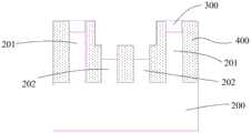
参考图4,提供衬底200,所述衬底200上具有分立排列的第一鳍部201以及第二鳍部202;在所述第一鳍部201和所述第二鳍部202顶部表面形成保护层300。Referring to FIG. 4 , a
所述衬底200、第一鳍部201、第二鳍部202以及所述保护层300的形成步骤包括:提供半导体基底(图未示);在所述半导体基底上形成第一图形化掩膜层(图未示)。所述第一图形化掩膜层定义第一鳍部201和第二鳍部202的位置和形状;以所述第一图形化掩膜层为掩膜,刻蚀所述半导体基底,形成所述衬底200、第一鳍部201、第二鳍部202以及位于第一鳍部201和第二鳍部202顶部的所述保护层300。The steps of forming the
所述半导体基底的材料包括硅、锗、锗化硅、砷化镓、铟镓砷等半导体材料,其中硅材料包括单晶硅、多晶硅或非晶硅。所述半导体基底还能够是绝缘体上半导体结构,所述绝缘体上半导体结构包括绝缘体及位于绝缘体上的半导体材料层,所述半导体材料层的材料包括硅、锗、锗化硅、砷化镓、铟镓砷等半导体材料。The material of the semiconductor substrate includes semiconductor materials such as silicon, germanium, silicon germanium, gallium arsenide, indium gallium arsenide, etc., wherein the silicon material includes single crystal silicon, polycrystalline silicon or amorphous silicon. The semiconductor substrate can also be a semiconductor-on-insulator structure, and the semiconductor-on-insulator structure includes an insulator and a semiconductor material layer on the insulator, and the material of the semiconductor material layer includes silicon, germanium, silicon germanium, gallium arsenide, indium Semiconductor materials such as gallium arsenide.
在本实施例中,所述半导体基底的材料为单晶硅。即所述衬底200、第一鳍部201、以及第二鳍部202的材料为单晶硅。In this embodiment, the material of the semiconductor substrate is single crystal silicon. That is, the
本实施例中,所述保护层300用于后续对隔离层进行平坦化时,保护所述第一鳍部201和第二鳍部202的顶部不受损伤,同时也作为后续隔离层平坦化时的终止层。In this embodiment, the
本实施例中,所述第一图形化掩膜层的形成工艺为化学气相沉积工艺。其他实施例中,所述第一图像化掩膜层的形成工艺还可以是物理气相沉积工艺或原子层沉积工艺。In this embodiment, the formation process of the first patterned mask layer is a chemical vapor deposition process. In other embodiments, the formation process of the first imaged mask layer may also be a physical vapor deposition process or an atomic layer deposition process.
本实施例中,所述保护层300的材料为氮化硅。其他实施例中,所述保护层300的材料包括氮碳化硅、氮硼化硅、氮碳氧化硅或氮氧化硅。In this embodiment, the material of the
在其他实施例中,所述衬底200、第一鳍部201、以及第二鳍部211的形成步骤还包括:提供半导体基底(未图示),在所述半导体基底上先形成初始保护层,在所述初始保护层上形成图形化层,以所述图形化层为掩膜,刻蚀所述初始保护层和所述半导体基底,以形成所述第一鳍部201、第二鳍部211以及位于第一鳍部201和第二鳍部211顶部的保护层300。In other embodiments, the steps of forming the
参考图5,在所述衬底200上形成隔离层400。所述隔离层400填充满所述第一鳍部201及所述第二鳍部202间的间隙。具体的,所述隔离层400覆盖所述第一鳍部201和第二鳍部202的侧壁,且暴露出所述第一鳍部201和第二鳍部202的顶部表面。Referring to FIG. 5 , an
所述隔离层400的形成步骤包括:在所述衬底200上形成隔离层400,所述隔离层400覆盖所述第一鳍部201和第二鳍部211的顶部表面;平坦化所述隔离层400。The steps of forming the
本实施例中,所述隔离层400的材料为氧化硅;其他实施例中,所述隔离层400的材料还可以是碳氧化硅、碳氮氧化硅或氮氧化硅。In this embodiment, the material of the
所述隔离层400的形成工艺为流体化学气相沉积工艺(Flowable Chemical VaporDeposition,简称FCVD)。所述流体化学气相沉积的工艺步骤包括:在所述衬底200上形成含硅的前驱体,所述含硅的前驱体覆盖所述第一鳍部201和第二鳍部202;对所述含硅的前驱体进行氧化处理形成初始隔离层(图未示);对所述初始隔离层进行退火处理形成隔离层400。The formation process of the
在其他实施例中,所述隔离层400还能够采用等离子体增强化学气相沉积工艺(PECVD)或者高深宽比化学气相沉积工艺(HARP)。In other embodiments, the
所述平坦化工艺为化学机械抛光工艺(CMP);在本实施例中,所述化学机械抛光工艺直至暴露出所述第一鳍部201和第二鳍部202的顶部的保护层300。The planarization process is a chemical mechanical polishing process (CMP); in this embodiment, the chemical mechanical polishing process is performed until the
参考图6,在所述第一鳍部201上形成掩膜层500,且所述掩膜层500覆盖所述隔离层400顶部的部分表面。Referring to FIG. 6 , a
所述掩膜层500的形成步骤包括:在所述保护层300以及所述隔离层400顶部表面形成初始掩膜层(未图示),在所述初始掩膜层上表面形成图形化光刻胶,所述图形化光刻胶定义第二鳍部202的位置和形状,以所述图形化光刻胶为掩膜刻蚀所述初始掩膜层,形成所述掩膜层500。The steps of forming the
本实施例中,所述掩膜层500的形成工艺为化学气相沉积工艺;其他实施例中,所述掩膜层500的形成工艺还可以是物理气相沉积工艺或原子层沉积工艺。In this embodiment, the formation process of the
本实施例中,所述掩膜层500的材料为氮化硅或碳氧化硅、碳氮氧化硅或氮氧化硅。In this embodiment, the material of the
本实施例中,所述掩膜层500的材料为氮化硅,所述掩膜层500的厚度为3nm~5nm。In this embodiment, the material of the
参考图7,以所述掩膜层500为掩膜,采用原子层刻蚀(ALE)工艺刻蚀所述隔离层400至露出所述衬底200以及所述第二鳍部202的侧壁表面。Referring to FIG. 7 , using the
采用原子层刻蚀工艺对所述隔离层400进行刻蚀时,以一种有序的方式在原子尺度逐层去除材料,能够实现定向刻蚀和高选择比,即使深宽比不同的情况下,也能实现等量刻蚀,能够实现精准控制。When the
本实施例中,控制所述原子层刻蚀工艺参数,使得以所述掩膜层500为掩膜刻蚀所述隔离层400时,垂直的将待刻蚀掉的部分所述隔离层去除。In this embodiment, the atomic layer etching process parameters are controlled so that when the
本实施例中,所述原子层刻蚀工艺参数包括:刻蚀气体包括He、NH3和NF3,刻蚀腔室压强为2torr至10torr,NH3流量为200sccm至500sccm,NF3流量为20sccm至200sccm,He流量为600sccm至2000sccm,刻蚀时间为20秒至100秒。In this embodiment, the atomic layer etching process parameters include: the etching gas includes He, NH3 and NF3 , the pressure of the etching chamber is 2torr to 10torr, the flow rate of NH3 is 200sccm to 500sccm, and the flow rate of NF3 is 20sccm to 200 sccm, the He flow rate was 600 sccm to 2000 sccm, and the etching time was 20 s to 100 s.
参考图8,去除所述掩膜层500(参考图7)。Referring to FIG. 8, the mask layer 500 (refer to FIG. 7) is removed.
本实施例中,去除所述掩膜层500的工艺为湿法刻蚀的方法。所述湿法刻蚀工艺的刻蚀溶液为稀释的氢氟酸溶液;其中,HF与H2O的体积比为1/1000~1/100。In this embodiment, the process of removing the
参考图9,去除所述第二鳍部202(参考图8),形成开口401。Referring to FIG. 9 , the second fins 202 (refer to FIG. 8 ) are removed to form
本实施例中,去除所述第二鳍部202并形成开口401的工艺为鳍部切割工艺,包括:干法刻蚀工艺或湿法刻蚀工艺的一种或多种组合。In this embodiment, the process of removing the
本实施例中,所述鳍部切割工艺为干法刻蚀工艺,所述干法刻蚀的工艺参数包括:采用的刻蚀气体包括HBr和Ar,其中,HBr的流速为10sccm~1000sccm,Ar的流速为10sccm~1000sccm。In this embodiment, the fin cutting process is a dry etching process, and the process parameters of the dry etching include: the used etching gas includes HBr and Ar, wherein the flow rate of HBr is 10 sccm to 1000 sccm, and the flow rate of Ar The flow rate is 10sccm ~ 1000sccm.
在其他实施例中,刻蚀去除的工艺参数包括:刻蚀气体为HBr、O2和Cl2,还向刻蚀腔室内通入He,刻蚀腔室压强为2毫托至50毫托,刻蚀的源功率为200瓦至2000瓦,刻蚀加偏压功率为10瓦至100瓦,HBr流量为50sccm至500sccm,O2流量为2sccm至20sccm,Cl2流量为10sccm至300sccm,He流量为50sccm至500sccm。In other embodiments, the process parameters for etching and removing include: the etching gas is HBr, O2 and Cl2 , and He is also introduced into the etching chamber, and the pressure of the etching chamber is 2 mtorr to 50 mtorr, The source power for etching is 200 watts to 2000 watts, the etch plus bias power is 10 watts to 100 watts, the HBr flow rate is 50sccm to 500sccm, theO2 flow rate is 2sccm to20sccm , the Cl2 flow rate is 10sccm to 300sccm, and the He flow rate is 50sccm to 500sccm.
其他实施例中,也可以采用湿法刻蚀工艺去除所述第二鳍部202。所述湿法刻蚀的工艺采用的刻蚀溶液可以是四甲基氢氧化氨(TMAH)溶液或KOH溶液。In other embodiments, the
湿法刻蚀溶液为四甲基氢氧化铵溶液,四甲基氢氧化铵溶液对硅和氧化硅具有很好的刻蚀选择比,在去除所述第二鳍部202的条件下对侧壁的氧化硅没有影响,能够保证形成所述开口401的形貌完整。The wet etching solution is a tetramethyl ammonium hydroxide solution. The tetramethyl ammonium hydroxide solution has a good etching selectivity ratio to silicon and silicon oxide. The silicon oxide has no influence, which can ensure that the topography of the
需要说明的是,在其他实施例中,可以在去除所述第二鳍部202之后,再去除所述掩膜层500。It should be noted that, in other embodiments, the
参考图10,以所述开口401为掩膜,刻蚀所述衬底200,形成凹槽402。Referring to FIG. 10 , using the
所述开口401是由所述第一鳍部201及剩余的所述隔离层400围成的。沿所述401向所述衬底200进行刻蚀目的是增大所述第一鳍部201之间的绝缘性,提高半导体的器件性能。The
形成所述凹槽402的工艺为干法刻蚀,工艺参数为:刻蚀气体包括He、NH3和NF3,刻蚀腔室压强为2torr至10torr,NH3流量为200sccm至500sccm,NF3流量为20sccm至200sccm,He流量为600sccm至2000sccm,刻蚀时间为20秒至100秒。The process for forming the
参考图11,继续以所述开口401为掩膜,沿所述凹槽402刻蚀所述衬底,加宽所述凹槽402。Referring to FIG. 11 , continuing to use the
采用回刻蚀的方法横向加宽所述凹槽,工艺参数为:刻蚀气体包括He、NH3和NF3,刻蚀腔室压强为2torr至10torr,NH3流量为200sccm至500sccm,NF3流量为20sccm至200sccm,He流量为600sccm至2000sccm,刻蚀时间为20秒至100秒。The groove is laterally widened by an etch-back method. The process parameters are: the etching gas includes He, NH3 and NF3 , the pressure of the etching chamber is 2torr to 10torr, the flow rate of NH3 is 200sccm to 500sccm, and the NF3 The flow rate is 20sccm to 200sccm, the He flow rate is 600sccm to 2000sccm, and the etching time is 20 seconds to 100 seconds.
加宽所述凹槽402的目的是进一步隔离所述第一鳍部201,提高所述第一鳍部201之间的绝缘性,进一步提高所述半导体器件的性能。The purpose of widening the
第二实施例Second Embodiment
本实施例与第一实施例的区别在于形成所述开口401的过程不同,如下将对区别部分进行详细叙述。The difference between this embodiment and the first embodiment is that the process of forming the
图12至图15是本发明另一实施例的半导体结构的形成过程的结构示意图。FIG. 12 to FIG. 15 are schematic structural diagrams of a process of forming a semiconductor structure according to another embodiment of the present invention.
参考图12,提供所述衬底200,所述衬底200上具有分立排列的第一鳍部201以及第二鳍部202;在所述第一鳍部201和所述第二鳍部202顶部表面形成保护层300;在所述衬底200上形成隔离层400,所述隔离层400填充满所述第一鳍部201及所述第二鳍部202间的间隙,所述隔离层400顶部表面与所述第一鳍部201及所述第二鳍部202顶部表面齐平;在所述第一鳍部201上形成掩膜层500,且所述掩膜层500覆盖所述隔离层400顶部的部分表面。Referring to FIG. 12 , the
本实施例中,所述掩膜层500的厚度为3nm~5nm。In this embodiment, the thickness of the
本实施例中上述各步骤的形成过程与第一实施例相同,在此不在赘述。The formation process of the above steps in this embodiment is the same as that of the first embodiment, and is not repeated here.
参考图13,以所述掩膜层500为掩膜,刻蚀部分高度所述隔离层400,至露出部分所述第二鳍部202的侧壁表面。Referring to FIG. 13 , using the
本实施例中,刻蚀工艺为原子层刻蚀(ALE)工艺。所述原子层刻蚀工艺的参数为:刻蚀气体包括He、NH3和NF3,刻蚀腔室压强为2torr至10torr,NH3流量为200sccm至500sccm,NF3流量为20sccm至200sccm,He流量为600sccm至2000sccm,刻蚀时间为20秒至100秒。In this embodiment, the etching process is an atomic layer etching (ALE) process. The parameters of the atomic layer etching process are: the etching gas includes He, NH3 and NF3 , the pressure of the etching chamber is 2torr to 10torr, the flow rate of NH3 is 200sccm to 500sccm, the flow rate of NF3 is 20sccm to 200sccm, and the flow rate of He The flow rate is 600sccm to 2000sccm, and the etching time is 20 seconds to 100 seconds.
采用所述原子层刻蚀工艺在刻蚀所述隔离层400时,由于所述原子层刻蚀工艺高选择性、良好的定向刻蚀性以及等量刻蚀的性质,使得暴露出的所述第二鳍部202的高度相同,并且在垂直向下刻蚀的过程中,不会发生偏移。When the
参考图14,去除所述掩膜层500(参考图13)以及所述第二鳍部202顶部表面的保护层300,并进一步刻蚀部分厚度所述第二鳍部202。Referring to FIG. 14 , the mask layer 500 (refer to FIG. 13 ) and the
本实施例中,去除所述掩膜层500(参考图13)以及部分厚度的所述第二鳍部202顶部表面的保护层300的工艺为原子层刻蚀工艺。In this embodiment, the process of removing the mask layer 500 (refer to FIG. 13 ) and a partial thickness of the
在其他实施例中,先使用湿法或干法刻蚀工艺将所述第二鳍部202顶部表面的所述保护层300去除,由于在本实施例中,所述第二鳍部202顶部表面的保护层300的材料以及所述掩膜层500的材料为氮化硅,在刻蚀掉所述第二鳍部202顶部表面的保护层300时,所述掩膜层500的厚度会变薄。然后使用原子层刻蚀工艺的高选择刻蚀性,对所述第二鳍部202进行刻蚀。In other embodiments, the
需要说明的是,所述掩膜层500最终要全部被去除掉,可以选择在形成所述开口401之前,也可以选择在形成所述开口401之后。It should be noted that, the
参考图15,重复上述步骤,使用所述原子层刻蚀工艺对氧化硅的选择刻蚀性对所述隔离层400进行部分厚度刻蚀,同时采用所述原子层刻蚀工艺对硅的选择刻蚀性对所述第二鳍部202进行部分厚度的刻蚀;如此循环,即采用所述原子层刻蚀工艺去除所述第二鳍部202与刻蚀所述隔离层400同步进行,去除掉所述第二鳍部202,以形成所述开口401。Referring to FIG. 15 , the above steps are repeated, and the
本实施例中,刻蚀部分厚度的所述隔离层400使得刻蚀的定向效果更好,进一步避免对高深宽比的刻蚀情况下发生偏移的情况,更好的保障刻蚀方向;同理,在刻蚀掉部分厚度所述隔离层400后,再刻蚀部分厚度的所述第二鳍部202,同样能够保障对所述第二鳍部202刻蚀时的方向;如此反复,每一次都避免高深宽比刻蚀会出现偏移的情况,使得最终完全去除所述第二鳍部202,不会而对所述第一鳍部201造成损伤;并且所形成的所述开口401的形状也更加完美,利于后续工艺进行。In this embodiment, the
本实施例中,所述原子层刻蚀工艺刻蚀所述隔离层400的工艺参数为:刻蚀气体包括He、NH3和NF3,刻蚀腔室压强为2torr至10torr,NH3流量为200sccm至500sccm,NF3流量为20sccm至200sccm,He流量为600sccm至2000sccm,刻蚀时间为20秒至100秒。In this embodiment, the process parameters of the atomic layer etching process for etching the
本实施例中,所述原子层刻蚀工艺刻蚀所述第二鳍部202的工艺参数为:刻蚀气体为HBr、O2和Cl2,还向刻蚀腔室内通入He,刻蚀腔室压强为2毫托至50毫托,刻蚀的源功率为200瓦至2000瓦,刻蚀加偏压功率为10瓦至100瓦,HBr流量为50sccm至500sccm,O2流量为2sccm至20sccm,Cl2流量为10sccm至300sccm,He流量为50sccm至500sccm。In this embodiment, the process parameters for etching the
请继续参考图10,以所述开口401为掩膜,刻蚀所述衬底200,形成凹槽402。Please continue to refer to FIG. 10 , using the
所述开口401是由所述第一鳍部201及剩余的所述隔离层400围成的。沿所述401向所述衬底200进行刻蚀目的是增大所述第一鳍部201之间的绝缘性,提高半导体的器件性能。The
形成所述凹槽402的工艺为干法刻蚀,工艺参数为:刻蚀气体包括He、NH3和NF3,刻蚀腔室压强为2torr至10torr,NH3流量为200sccm至500sccm,NF3流量为20sccm至200sccm,He流量为600sccm至2000sccm,刻蚀时间为20秒至100秒。The process for forming the
请继续参考图11,继续以所述开口401为掩膜,沿所述凹槽402刻蚀所述衬底,加宽所述凹槽402。Please continue to refer to FIG. 11 , continue to use the
采用回刻蚀的方法横向加宽所述凹槽,工艺参数为:刻蚀气体包括He、NH3和NF3,刻蚀腔室压强为2torr至10torr,NH3流量为200sccm至500sccm,NF3流量为20sccm至200sccm,He流量为600sccm至2000sccm,刻蚀时间为20秒至100秒。The groove is laterally widened by etching back, and the process parameters are: the etching gas includes He, NH3 and NF3, the etching chamber pressure is 2torr to 10torr, the flow rate of NH3 is 200sccm to 500sccm, and the flow rate of NF3 is 20sccm to 200sccm, the He flow rate is 600sccm to 2000sccm, and the etching time is 20 seconds to 100 seconds.
加宽所述凹槽402的目的是进一步隔离所述第一鳍部201,提高所述第一鳍部201之间的绝缘性,进一步提高所述半导体器件的性能。The purpose of widening the
虽然本发明披露如上,但本发明并非限定于此。任何本领域技术人员,在不脱离本发明的精神和范围内,均可作各种更动与修改,因此本发明的保护范围应当以权利要求所限定的范围为准。Although the present invention is disclosed above, the present invention is not limited thereto. Any person skilled in the art can make various changes and modifications without departing from the spirit and scope of the present invention. Therefore, the protection scope of the present invention should be based on the scope defined by the claims.
Claims (14)
Translated fromChinesePriority Applications (1)
| Application Number | Priority Date | Filing Date | Title |
|---|---|---|---|
| CN201910545011.0ACN112117192B (en) | 2019-06-21 | 2019-06-21 | Method for forming semiconductor structure |
Applications Claiming Priority (1)
| Application Number | Priority Date | Filing Date | Title |
|---|---|---|---|
| CN201910545011.0ACN112117192B (en) | 2019-06-21 | 2019-06-21 | Method for forming semiconductor structure |
Publications (2)
| Publication Number | Publication Date |
|---|---|
| CN112117192Atrue CN112117192A (en) | 2020-12-22 |
| CN112117192B CN112117192B (en) | 2024-09-17 |
Family
ID=73796308
Family Applications (1)
| Application Number | Title | Priority Date | Filing Date |
|---|---|---|---|
| CN201910545011.0AActiveCN112117192B (en) | 2019-06-21 | 2019-06-21 | Method for forming semiconductor structure |
Country Status (1)
| Country | Link |
|---|---|
| CN (1) | CN112117192B (en) |
Cited By (1)
| Publication number | Priority date | Publication date | Assignee | Title |
|---|---|---|---|---|
| CN114695117A (en)* | 2020-12-29 | 2022-07-01 | 广州集成电路技术研究院有限公司 | A FinFET device and its formation method and electronic device |
Citations (4)
| Publication number | Priority date | Publication date | Assignee | Title |
|---|---|---|---|---|
| US20150249127A1 (en)* | 2014-03-03 | 2015-09-03 | Globalfoundries Inc. | Methods of forming fins for finfet semiconductor devices and selectively removing some of the fins by performing a cyclical fin cutting process |
| CN108022880A (en)* | 2016-11-04 | 2018-05-11 | 中芯国际集成电路制造(上海)有限公司 | The forming method of semiconductor structure |
| CN108962990A (en)* | 2017-05-23 | 2018-12-07 | 中芯国际集成电路制造(上海)有限公司 | Semiconductor structure and forming method thereof |
| CN109411415A (en)* | 2018-09-07 | 2019-03-01 | 上海集成电路研发中心有限公司 | A kind of forming method of semiconductor structure |
- 2019
- 2019-06-21CNCN201910545011.0Apatent/CN112117192B/enactiveActive
Patent Citations (4)
| Publication number | Priority date | Publication date | Assignee | Title |
|---|---|---|---|---|
| US20150249127A1 (en)* | 2014-03-03 | 2015-09-03 | Globalfoundries Inc. | Methods of forming fins for finfet semiconductor devices and selectively removing some of the fins by performing a cyclical fin cutting process |
| CN108022880A (en)* | 2016-11-04 | 2018-05-11 | 中芯国际集成电路制造(上海)有限公司 | The forming method of semiconductor structure |
| CN108962990A (en)* | 2017-05-23 | 2018-12-07 | 中芯国际集成电路制造(上海)有限公司 | Semiconductor structure and forming method thereof |
| CN109411415A (en)* | 2018-09-07 | 2019-03-01 | 上海集成电路研发中心有限公司 | A kind of forming method of semiconductor structure |
Cited By (2)
| Publication number | Priority date | Publication date | Assignee | Title |
|---|---|---|---|---|
| CN114695117A (en)* | 2020-12-29 | 2022-07-01 | 广州集成电路技术研究院有限公司 | A FinFET device and its formation method and electronic device |
| WO2022143586A1 (en)* | 2020-12-29 | 2022-07-07 | 广州集成电路技术研究院有限公司 | Finfet device and forming method therefor, and electronic device |
Also Published As
| Publication number | Publication date |
|---|---|
| CN112117192B (en) | 2024-09-17 |
Similar Documents
| Publication | Publication Date | Title |
|---|---|---|
| CN108321079B (en) | Semiconductor structure and forming method thereof | |
| CN104008994B (en) | Manufacturing method of semiconductor device | |
| US9379220B2 (en) | FinFET device structure and methods of making same | |
| TWI713089B (en) | Methods for forming integrated circuit structure | |
| CN110690117B (en) | Semiconductor structure and forming method thereof | |
| CN104900495B (en) | The preparation method of self-alignment duplex pattern method and fin formula field effect transistor | |
| CN107039272B (en) | Method for forming fin type transistor | |
| CN104752185B (en) | The forming method of metal gates | |
| CN108321090B (en) | Semiconductor device and method of forming the same | |
| CN106952816B (en) | Method of forming a fin transistor | |
| CN111129142A (en) | Semiconductor device and method of forming the same | |
| CN109285875B (en) | Fin transistor and method of forming the same | |
| CN108807377B (en) | Semiconductor device and method of forming the same | |
| CN108155149B (en) | Fin field effect transistor forming method and semiconductor structure | |
| CN109585289B (en) | Semiconductor device and method of forming the same | |
| CN109980003A (en) | Semiconductor devices and forming method thereof | |
| CN109872953B (en) | Semiconductor device and method of forming the same | |
| US11145760B2 (en) | Structure having improved fin critical dimension control | |
| CN111863614B (en) | Semiconductor structures and methods of forming them | |
| CN114388352A (en) | Semiconductor structure and forming method thereof | |
| CN112117192B (en) | Method for forming semiconductor structure | |
| CN112151382A (en) | Semiconductor structure and forming method thereof | |
| US11652003B2 (en) | Gate formation process | |
| CN112563200B (en) | Semiconductor device and method of forming the same | |
| CN107170685B (en) | Method for forming fin type transistor |
Legal Events
| Date | Code | Title | Description |
|---|---|---|---|
| PB01 | Publication | ||
| PB01 | Publication | ||
| SE01 | Entry into force of request for substantive examination | ||
| SE01 | Entry into force of request for substantive examination | ||
| GR01 | Patent grant | ||
| GR01 | Patent grant |