CN112114700A - Sensor assembly and display device - Google Patents
Sensor assembly and display deviceDownload PDFInfo
- Publication number
- CN112114700A CN112114700ACN202010914028.1ACN202010914028ACN112114700ACN 112114700 ACN112114700 ACN 112114700ACN 202010914028 ACN202010914028 ACN 202010914028ACN 112114700 ACN112114700 ACN 112114700A
- Authority
- CN
- China
- Prior art keywords
- electrode
- thin film
- film transistor
- sensor assembly
- substrate
- Prior art date
- Legal status (The legal status is an assumption and is not a legal conclusion. Google has not performed a legal analysis and makes no representation as to the accuracy of the status listed.)
- Pending
Links
Images


Classifications
- G—PHYSICS
- G02—OPTICS
- G02F—OPTICAL DEVICES OR ARRANGEMENTS FOR THE CONTROL OF LIGHT BY MODIFICATION OF THE OPTICAL PROPERTIES OF THE MEDIA OF THE ELEMENTS INVOLVED THEREIN; NON-LINEAR OPTICS; FREQUENCY-CHANGING OF LIGHT; OPTICAL LOGIC ELEMENTS; OPTICAL ANALOGUE/DIGITAL CONVERTERS
- G02F1/00—Devices or arrangements for the control of the intensity, colour, phase, polarisation or direction of light arriving from an independent light source, e.g. switching, gating or modulating; Non-linear optics
- G02F1/01—Devices or arrangements for the control of the intensity, colour, phase, polarisation or direction of light arriving from an independent light source, e.g. switching, gating or modulating; Non-linear optics for the control of the intensity, phase, polarisation or colour
- G02F1/13—Devices or arrangements for the control of the intensity, colour, phase, polarisation or direction of light arriving from an independent light source, e.g. switching, gating or modulating; Non-linear optics for the control of the intensity, phase, polarisation or colour based on liquid crystals, e.g. single liquid crystal display cells
- G02F1/133—Constructional arrangements; Operation of liquid crystal cells; Circuit arrangements
- G02F1/1333—Constructional arrangements; Manufacturing methods
- G02F1/13338—Input devices, e.g. touch panels
- G—PHYSICS
- G06—COMPUTING OR CALCULATING; COUNTING
- G06F—ELECTRIC DIGITAL DATA PROCESSING
- G06F3/00—Input arrangements for transferring data to be processed into a form capable of being handled by the computer; Output arrangements for transferring data from processing unit to output unit, e.g. interface arrangements
- G06F3/01—Input arrangements or combined input and output arrangements for interaction between user and computer
- G06F3/03—Arrangements for converting the position or the displacement of a member into a coded form
- G06F3/041—Digitisers, e.g. for touch screens or touch pads, characterised by the transducing means
- G06F3/0412—Digitisers structurally integrated in a display
- G—PHYSICS
- G06—COMPUTING OR CALCULATING; COUNTING
- G06F—ELECTRIC DIGITAL DATA PROCESSING
- G06F3/00—Input arrangements for transferring data to be processed into a form capable of being handled by the computer; Output arrangements for transferring data from processing unit to output unit, e.g. interface arrangements
- G06F3/01—Input arrangements or combined input and output arrangements for interaction between user and computer
- G06F3/03—Arrangements for converting the position or the displacement of a member into a coded form
- G06F3/041—Digitisers, e.g. for touch screens or touch pads, characterised by the transducing means
- G06F3/0416—Control or interface arrangements specially adapted for digitisers
- G06F3/04164—Connections between sensors and controllers, e.g. routing lines between electrodes and connection pads
- G—PHYSICS
- G06—COMPUTING OR CALCULATING; COUNTING
- G06F—ELECTRIC DIGITAL DATA PROCESSING
- G06F3/00—Input arrangements for transferring data to be processed into a form capable of being handled by the computer; Output arrangements for transferring data from processing unit to output unit, e.g. interface arrangements
- G06F3/01—Input arrangements or combined input and output arrangements for interaction between user and computer
- G06F3/03—Arrangements for converting the position or the displacement of a member into a coded form
- G06F3/041—Digitisers, e.g. for touch screens or touch pads, characterised by the transducing means
- G06F3/042—Digitisers, e.g. for touch screens or touch pads, characterised by the transducing means by opto-electronic means
- G06F3/0421—Digitisers, e.g. for touch screens or touch pads, characterised by the transducing means by opto-electronic means by interrupting or reflecting a light beam, e.g. optical touch-screen
- G—PHYSICS
- G06—COMPUTING OR CALCULATING; COUNTING
- G06F—ELECTRIC DIGITAL DATA PROCESSING
- G06F3/00—Input arrangements for transferring data to be processed into a form capable of being handled by the computer; Output arrangements for transferring data from processing unit to output unit, e.g. interface arrangements
- G06F3/01—Input arrangements or combined input and output arrangements for interaction between user and computer
- G06F3/03—Arrangements for converting the position or the displacement of a member into a coded form
- G06F3/041—Digitisers, e.g. for touch screens or touch pads, characterised by the transducing means
- G06F3/044—Digitisers, e.g. for touch screens or touch pads, characterised by the transducing means by capacitive means
- G06F3/0445—Digitisers, e.g. for touch screens or touch pads, characterised by the transducing means by capacitive means using two or more layers of sensing electrodes, e.g. using two layers of electrodes separated by a dielectric layer
- G—PHYSICS
- G06—COMPUTING OR CALCULATING; COUNTING
- G06F—ELECTRIC DIGITAL DATA PROCESSING
- G06F3/00—Input arrangements for transferring data to be processed into a form capable of being handled by the computer; Output arrangements for transferring data from processing unit to output unit, e.g. interface arrangements
- G06F3/01—Input arrangements or combined input and output arrangements for interaction between user and computer
- G06F3/03—Arrangements for converting the position or the displacement of a member into a coded form
- G06F3/041—Digitisers, e.g. for touch screens or touch pads, characterised by the transducing means
- G06F3/044—Digitisers, e.g. for touch screens or touch pads, characterised by the transducing means by capacitive means
- G06F3/0446—Digitisers, e.g. for touch screens or touch pads, characterised by the transducing means by capacitive means using a grid-like structure of electrodes in at least two directions, e.g. using row and column electrodes
- H—ELECTRICITY
- H10—SEMICONDUCTOR DEVICES; ELECTRIC SOLID-STATE DEVICES NOT OTHERWISE PROVIDED FOR
- H10F—INORGANIC SEMICONDUCTOR DEVICES SENSITIVE TO INFRARED RADIATION, LIGHT, ELECTROMAGNETIC RADIATION OF SHORTER WAVELENGTH OR CORPUSCULAR RADIATION
- H10F39/00—Integrated devices, or assemblies of multiple devices, comprising at least one element covered by group H10F30/00, e.g. radiation detectors comprising photodiode arrays
- H10F39/10—Integrated devices
- H10F39/12—Image sensors
- H10F39/18—Complementary metal-oxide-semiconductor [CMOS] image sensors; Photodiode array image sensors
- H—ELECTRICITY
- H10—SEMICONDUCTOR DEVICES; ELECTRIC SOLID-STATE DEVICES NOT OTHERWISE PROVIDED FOR
- H10F—INORGANIC SEMICONDUCTOR DEVICES SENSITIVE TO INFRARED RADIATION, LIGHT, ELECTROMAGNETIC RADIATION OF SHORTER WAVELENGTH OR CORPUSCULAR RADIATION
- H10F39/00—Integrated devices, or assemblies of multiple devices, comprising at least one element covered by group H10F30/00, e.g. radiation detectors comprising photodiode arrays
- H10F39/80—Constructional details of image sensors
- H10F39/805—Coatings
- H10F39/8057—Optical shielding
- G—PHYSICS
- G06—COMPUTING OR CALCULATING; COUNTING
- G06F—ELECTRIC DIGITAL DATA PROCESSING
- G06F2203/00—Indexing scheme relating to G06F3/00 - G06F3/048
- G06F2203/041—Indexing scheme relating to G06F3/041 - G06F3/045
- G06F2203/04106—Multi-sensing digitiser, i.e. digitiser using at least two different sensing technologies simultaneously or alternatively, e.g. for detecting pen and finger, for saving power or for improving position detection
Landscapes
- Engineering & Computer Science (AREA)
- General Engineering & Computer Science (AREA)
- Physics & Mathematics (AREA)
- Theoretical Computer Science (AREA)
- General Physics & Mathematics (AREA)
- Human Computer Interaction (AREA)
- Nonlinear Science (AREA)
- Chemical & Material Sciences (AREA)
- Crystallography & Structural Chemistry (AREA)
- Mathematical Physics (AREA)
- Optics & Photonics (AREA)
- Computer Networks & Wireless Communication (AREA)
- Devices For Indicating Variable Information By Combining Individual Elements (AREA)
- Liquid Crystal (AREA)
Abstract
Description
Translated fromChinese技术领域technical field
本申请涉及显示面板技术领域,尤其涉及一种传感器组件及显示装置。The present application relates to the technical field of display panels, and in particular, to a sensor assembly and a display device.
背景技术Background technique
随着显示技术的发展,将传感器集成在显示面板之中也是一种趋势,但目前大多数显示器将传感器贴合在显示器的外面,这样会导致显示面板的光效下降和成本的上升。With the development of display technology, it is also a trend to integrate sensors into display panels, but at present, most displays attach sensors to the outside of the display, which will reduce the light efficiency of the display panel and increase the cost.
而部分液晶显示器中集成有触控传感器,但没有液晶显示器同时集成触控传感器和光控传感器,无法满足用户对触控和光控功能的同时需求,导致液晶显示器的功能单一。Some liquid crystal displays integrate a touch sensor, but no liquid crystal display integrates a touch sensor and a light control sensor at the same time, which cannot meet the simultaneous needs of users for touch and light control functions, resulting in a single function of the liquid crystal display.
发明内容SUMMARY OF THE INVENTION
本申请实施例提供一种传感器组件及显示装置,以解决现有技术无法同时集成触控传感器和光控传感器的问题。Embodiments of the present application provide a sensor assembly and a display device to solve the problem that a touch sensor and a light control sensor cannot be simultaneously integrated in the prior art.
本申请实施例提供了一种传感器组件,包括衬底,以及位于所述衬底上的触控传感器和光控传感器;所述触控传感器包括发射电极以及位于所述发射电极背离所述衬底一侧的接收电极,所述光控传感器包括薄膜晶体管组件;An embodiment of the present application provides a sensor assembly, including a substrate, and a touch sensor and a light control sensor located on the substrate; the touch sensor includes an emitter electrode and a sensor located on the emitter electrode away from the substrate a receiving electrode on one side, the light control sensor includes a thin film transistor assembly;
所述薄膜晶体管组件的栅极与所述发射电极同层设置,所述薄膜晶体管组件的源漏极与所述接收电极同层设置。The gate electrode of the thin film transistor element is arranged on the same layer as the emitter electrode, and the source and drain electrodes of the thin film transistor element are arranged on the same layer as the receiving electrode.
进一步地,所述光控传感器还包括与所述薄膜晶体管组件电性连接的多个扫描线和多个数据线;Further, the light control sensor further includes a plurality of scan lines and a plurality of data lines electrically connected to the thin film transistor assembly;
所述多个扫描线与所述发射电极同层设置,所述多个数据线与所述接收电极同层设置。The plurality of scan lines are arranged on the same layer as the transmitting electrodes, and the plurality of data lines are arranged on the same layer as the receiving electrodes.
进一步地,所述发射电极包括多行第一电极单元,且行方向上任意相邻的两个第一电极单元电性连接;所述接收电极包括多列第二电极单元,且列方向上任意相邻的两个第二电极单元电性连接;所述多行第一电极单元在所述衬底上的正投影与所述多列第二电极单元在所述衬底上的正投影相交叉,以构成互容式电极结构;Further, the transmitting electrode includes multiple rows of first electrode units, and any two adjacent first electrode units in the row direction are electrically connected; the receiving electrode includes multiple columns of second electrode units, and any phase in the column direction is arranged. Two adjacent second electrode units are electrically connected; the orthographic projections of the first electrode units in the plurality of rows on the substrate intersect with the orthographic projections of the second electrode units in the plurality of columns on the substrate, To form a mutual capacitance electrode structure;
任意相邻的两行第一电极单元之间设有一个扫描线,任意相邻的两列第二电极单元之间设有一个数据线。A scan line is arranged between any two adjacent rows of the first electrode units, and a data line is arranged between any two adjacent columns of the second electrode units.
进一步地,所述传感器组件包括多个交叉区,任意一个扫描线在所述衬底上的正投影与任意一个数据线在所述衬底上的正投影相交于一个交叉区内;Further, the sensor assembly includes a plurality of intersection areas, and the orthographic projection of any scan line on the substrate intersects with the orthographic projection of any data line on the substrate in one intersection area;
所述薄膜晶体管组件包括对应设于所述多个交叉区中的多个薄膜晶体管结构。The thin film transistor assembly includes a plurality of thin film transistor structures correspondingly disposed in the plurality of intersection regions.
进一步地,每个交叉区中的薄膜晶体管结构包括光感晶体管和开关晶体管;Further, the thin film transistor structure in each cross region includes a phototransistor and a switch transistor;
所述光感晶体管的漏极与对应的数据线连接,所述开关晶体管的栅极与对应的扫描线连接,所述光感晶体管的源极与所述开关晶体管的漏极连接。The drain of the phototransistor is connected to the corresponding data line, the gate of the switch transistor is connected to the corresponding scan line, and the source of the phototransistor is connected to the drain of the switch transistor.
进一步地,每个扫描线包括与其相邻的两行第一电极单元对应设置的两个子扫描线,每个子扫描线沿其对应的一行第一电极单元的侧边延伸;Further, each scan line includes two sub-scan lines corresponding to two adjacent rows of first electrode units, and each sub-scan line extends along the side of its corresponding row of first electrode units;
每个数据线包括与其相邻的两列第二电极单元对应设置的两个子数据线,每个子数据线沿其对应的一列第二电极单元的侧边延伸。Each data line includes two sub-data lines corresponding to two adjacent columns of second electrode units, and each sub-data line extends along the side of a corresponding column of second electrode units.
进一步地,所述第一电极单元和所述第二电极单元均为网格状结构,所述网格状结构中的网格呈三角形、四边形、六边形和八边形中的任意一种或多种。Further, the first electrode unit and the second electrode unit are both grid-like structures, and the grids in the grid-like structure are any one of triangles, quadrilaterals, hexagons and octagons or more.
进一步地,所述第一电极单元和所述第二电极单元在行方向上的长度范围均为1mm至8mm;所述网格状结构中的网格在行方向上的长度范围为0.1mm至4mm。Further, the lengths of the first electrode unit and the second electrode unit in the row direction are both in the range of 1 mm to 8 mm; the lengths of the grids in the grid-like structure in the row direction are in the range of 0.1 mm to 4 mm.
进一步地,所述薄膜晶体管结构背离所述衬底的一侧还设有黑矩阵;Further, a black matrix is further provided on the side of the thin film transistor structure away from the substrate;
所述黑矩阵与所述薄膜晶体管结构中的开关晶体管的位置相对应。The black matrix corresponds to the position of the switching transistors in the thin film transistor structure.
本申请实施例还提供了一种显示装置,包括显示面板以及上述传感器组件;Embodiments of the present application further provide a display device, including a display panel and the above sensor assembly;
所述传感器组件位于所述显示面板上。The sensor assembly is located on the display panel.
本申请的有益效果为:通过在衬底上设置触控传感器和光控传感器,使触控传感器的发射电极与光控传感器中的薄膜晶体管组件的栅极同层设置,触控传感器的接收电极与光控传感器中的薄膜晶体管组件的源漏极同层设置,实现触控传感器与光控传感器的同步集成,实现对显示面板的短程触控、远程光控功能。The beneficial effects of the present application are as follows: by arranging the touch sensor and the light control sensor on the substrate, the emitter electrode of the touch sensor and the gate of the thin film transistor component in the light control sensor are arranged in the same layer, and the receiving electrode of the touch sensor is arranged in the same layer. It is arranged in the same layer as the source and drain of the thin film transistor component in the light control sensor, realizing the synchronous integration of the touch sensor and the light control sensor, and realizing the short-range touch and remote light control functions of the display panel.
附图说明Description of drawings
下面结合附图,通过对本申请的具体实施方式详细描述,将使本申请的技术方案及其它有益效果显而易见。The technical solutions and other beneficial effects of the present application will be apparent through the detailed description of the specific embodiments of the present application in conjunction with the accompanying drawings.
图1为本申请实施例提供的传感器组件的结构示意图;FIG. 1 is a schematic structural diagram of a sensor assembly provided by an embodiment of the present application;
图2为本申请实施例提供的传感器组件中第一金属层的结构示意图;FIG. 2 is a schematic structural diagram of a first metal layer in a sensor assembly according to an embodiment of the present application;
图3为本申请实施例提供的传感器组件中第二金属层的结构示意图;FIG. 3 is a schematic structural diagram of a second metal layer in a sensor assembly provided by an embodiment of the present application;
图4为本申请实施例提供的传感器组件中触控传感器和光控传感器的位置关系简化图;4 is a simplified diagram of a positional relationship between a touch sensor and a light control sensor in a sensor assembly provided by an embodiment of the present application;
图5为本申请实施例提供的传感器组件中第一电极单元和第二电极单元的结构示意图;5 is a schematic structural diagram of a first electrode unit and a second electrode unit in the sensor assembly provided by the embodiment of the present application;
图6为本申请实施例提供的传感器组件中感应单元的电路图;6 is a circuit diagram of a sensing unit in a sensor assembly provided by an embodiment of the present application;
图7为本申请实施例提供的显示装置的结构示意图。FIG. 7 is a schematic structural diagram of a display device provided by an embodiment of the present application.
具体实施方式Detailed ways
这里所公开的具体结构和功能细节仅仅是代表性的,并且是用于描述本申请的示例性实施例的目的。但是本申请可以通过许多替换形式来具体实现,并且不应当被解释成仅仅受限于这里所阐述的实施例。Specific structural and functional details disclosed herein are merely representative and for purposes of describing example embodiments of the present application. The application may, however, be embodied in many alternative forms and should not be construed as limited only to the embodiments set forth herein.
在本申请的描述中,需要理解的是,术语“中心”、“横向”、“上”、“下”、“左”、“右”、“竖直”、“水平”、“顶”、“底”、“内”、“外”等指示的方位或位置关系为基于附图所示的方位或位置关系,仅是为了便于描述本申请和简化描述,而不是指示或暗示所指的装置或元件必须具有特定的方位、以特定的方位构造和操作,因此不能理解为对本申请的限制。此外,术语“第一”、“第二”仅用于描述目的,而不能理解为指示或暗示相对重要性或者隐含指明所指示的技术特征的数量。由此,限定有“第一”、“第二”的特征可以明示或者隐含地包括一个或者更多个该特征。在本申请的描述中,除非另有说明,“多个”的含义是两个或两个以上。另外,术语“包括”及其任何变形,意图在于覆盖不排他的包含。In the description of this application, it should be understood that the terms "center", "lateral", "top", "bottom", "left", "right", "vertical", "horizontal", "top", The orientation or positional relationship indicated by "bottom", "inner", "outer", etc. is based on the orientation or positional relationship shown in the accompanying drawings, which is only for the convenience of describing the present application and simplifying the description, rather than indicating or implying the indicated device. Or elements must have a particular orientation, be constructed and operate in a particular orientation, and therefore should not be construed as a limitation of the present application. In addition, the terms "first" and "second" are only used for descriptive purposes, and should not be construed as indicating or implying relative importance or implying the number of indicated technical features. Thus, a feature defined as "first" or "second" may expressly or implicitly include one or more of that feature. In the description of this application, unless stated otherwise, "plurality" means two or more. Additionally, the term "comprising" and any variations thereof are intended to cover non-exclusive inclusion.
在本申请的描述中,需要说明的是,除非另有明确的规定和限定,术语“安装”、“相连”、“连接”应做广义理解,例如,可以是固定连接,也可以是可拆卸连接,或一体地连接;可以是机械连接,也可以是电连接;可以是直接相连,也可以通过中间媒介间接相连,可以是两个元件内部的连通。对于本领域的普通技术人员而言,可以具体情况理解上述术语在本申请中的具体含义。In the description of this application, it should be noted that, unless otherwise expressly specified and limited, the terms "installed", "connected" and "connected" should be understood in a broad sense, for example, it may be a fixed connection or a detachable connection Connection, or integral connection; can be mechanical connection, can also be electrical connection; can be directly connected, can also be indirectly connected through an intermediate medium, can be internal communication between two elements. For those of ordinary skill in the art, the specific meanings of the above terms in this application can be understood in specific situations.
这里所使用的术语仅仅是为了描述具体实施例而不意图限制示例性实施例。除非上下文明确地另有所指,否则这里所使用的单数形式“一个”、“一项”还意图包括复数。还应当理解的是,这里所使用的术语“包括”和/或“包含”规定所陈述的特征、整数、步骤、操作、单元和/或组件的存在,而不排除存在或添加一个或更多其他特征、整数、步骤、操作、单元、组件和/或其组合。The terminology used herein is for the purpose of describing specific embodiments only and is not intended to limit the exemplary embodiments. As used herein, the singular forms "a", "an" and "an" are intended to include the plural unless the context clearly dictates otherwise. It should also be understood that the terms "comprising" and/or "comprising" as used herein specify the presence of stated features, integers, steps, operations, units and/or components, but do not preclude the presence or addition of one or more Other features, integers, steps, operations, units, components and/or combinations thereof.
下面结合附图和实施例对本申请作进一步说明。The present application will be further described below with reference to the accompanying drawings and embodiments.
如图1所示,本申请实施例提供了一种传感器组件,包括衬底1,以及位于衬底1上的触控传感器2和光控传感器3。其中,触控传感器2包括位于衬底1上的发射电极21,光控传感器3包括薄膜晶体管组件30和电容组件(图中未示出),薄膜晶体管组件30的栅极31位于衬底1上,即触控传感器2的发射电极21与薄膜晶体管组件30的栅极31同层设置。传感器组件还包括覆盖发射电极21、栅极31和衬底1的栅极绝缘层4,触控传感器2还包括位于栅极绝缘层4上的接收电极22,薄膜晶体组件30还包括位于栅极绝缘层4上的有源层32,以及位于栅极绝缘层4和有源层32上的源漏极33,即触控传感器2的接收电极22与薄膜晶体管组件30的源漏极33同层设置,从而将触控传感器2和光控传感器3同时集成在传感器组件中,实现对显示面板短程触控,远程光控的功能。其中,有源层32的材料可以为氢化非晶硅a-Si:H。As shown in FIG. 1 , an embodiment of the present application provides a sensor assembly including a substrate 1 , and a
进一步地,光控传感器3还包括与薄膜晶体管组件30电性连接的多个扫描线34和多个数据线35。多个扫描线34与多个数据线35位于不同膜层,多个扫描线34位于衬底1上,即多个扫描线34与触控传感器2的发射电极21、薄膜晶体管组件30的源极31同层设置,构成第一金属层,如图2所示;多个数据线35位于栅极绝缘层4上,即多个数据线35与触控传感器2的接收电极22、薄膜晶体管组件的源漏极33同层设置,构成第二金属层,如图3所示。Further, the
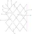
具体地,如图2所示,发射电极21包括多行第一电极单元23,且行方向上任意相邻的两个第一电极单元23电性连接,多个扫描线34与多行第一电极单元23交替设置,即任意相邻的两行第一电极单元23之间设有一个扫描线34,每个扫描线34沿行方向延伸。Specifically, as shown in FIG. 2 , the
如图3所示,接收电极22包括多列第二电极单元24,且列方向上任意相邻的两个第二电极单元24电性连接,多个数据线35与多列第二电极单元24交替设置,即任意相邻的两列第二电极单元24之间设有一个数据线35,每个数据线35沿列方向延伸。As shown in FIG. 3 , the receiving
多行第一电极单元23在衬底1上的正投影与多列第二电极单元24在衬底1上的正投影相交叉,且每行第一电极单元23与每列第二电极单元24的交叉位置对应的区域构成一个交叉区25,如图4所示。相交叉的多行第一电极单元23与多列第二电极单元24构成互容式电极结构。The orthographic projections of the plurality of rows of the
第一电极单元23和第二电极单元24的整体形状可以为菱形,且第一电极单元23和第二电极单元24在行方向上的长度D1范围均为1mm至8mm,如图5所示。另外,第一电极单元23和第二电极单元24均为网格状结构,网格状结构中的网格呈三角形、四边形、六边形和八边形中的任意一种或多种,且网格状结构中的网格26在行方向上的长度D2范围为0.1mm至4mm,如图5所示。The overall shape of the
多个扫描线34在衬底1上的正投影与多个数据线35在衬底1上的正投影相交叉,且每个扫描线34与每个数据线35的交叉位置对应的区域构成一个交叉区36,即任意一个扫描线34在衬底1上的正投影与任意一个数据线35在衬底1上的正投影相交于一个交叉区36内,如图4所示。交叉区36在扫描线34上的位置为列方向上相邻两个第一电极单元23之间,交叉区36在数据线35上的位置为行方向上相邻两个第二电极单元24之间。The orthographic projections of the plurality of
任意相邻的两行第一电极单元23之间的扫描线34可以包括两个子扫描线341,且两个子扫描线341与该两行第一电极单元23一一对应设置,每个子扫描线341沿其对应的一行第一电极单元23的侧边延伸。如图2所示,一行第一电极单元23中的每个第一电极单元23均为菱形,则该行第一电极单元23靠近子扫描线341的侧边在行方向上呈波浪形,对应的子扫描线341与该侧边平行设置,在行方向上呈波浪形延伸。每个子扫描线341与其对应的一行第一电极单元23之间具有间隙,以保证子扫描线341与第一电极单元23相互绝缘。另外,一个扫描线34的两个子扫描线341可以在该扫描线34对应的交叉区36中相交。The
任意相邻的两列第二电极单元24之间的数据线35可以包括两个子数据线351,且两个子数据线351与该两列第二电极单元24一一对应设置,每个子数据线351沿其对应的一列第二电极单元24的侧边延伸。如图3所示,一列第二电极单元24中的每个第二电极单元24均为菱形,则该列第二电极单元24靠近子数据线351的侧边在列方向上呈波浪形,对应的子扫描线341与该侧边平行设置,在行方向上呈波浪形延伸。每个子数据线351与其对应的一列第二电极单元24之间具有间隙,以保证子数据线351与第二电极单元24相互绝缘。另外,一个数据线35的两个子数据线351可以在该数据线35对应的交叉区36中相交。The data lines 35 between any two adjacent columns of
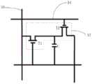
如图4所示,薄膜晶体管组件30包括多个薄膜晶体管结构37,薄膜晶体管组件30的栅极包括多个薄膜晶体管结构37的栅极,薄膜晶体管组件30的源漏极包括多个薄膜晶体管结构37的源漏极。电容组件包括多个电容,且多个电容与多个薄膜晶体管结构37一一对应连接,使每个薄膜晶体管结构37与其对应的电容构成一个感应单元,且感应单元的个数与交叉区36的个数相同,即每个交叉区36处设有一个感应单元,即每个交叉区36包括一个薄膜晶体管结构37。由于一个交叉区36对应一个扫描线34和一个数据线35,因此一个交叉区36中的薄膜晶体管结构37分别与该交叉区36对应的扫描线34和数据线35电性连接。交叉区36中的薄膜晶体管结构37的栅极位于列方向上相邻两个第一电极单元23之间,交叉区36中的薄膜晶体管结构37的源漏极位于行方向上相邻两个第二电极单元24之间。As shown in FIG. 4 , the thin
由于将触控传感器2和光控传感器3同步集成,光控传感器3的电极与触控传感器2的电极之间会存在寄生电容,影响触控传感器2的正常工作,即光控传感器3会对触控传感器2造成信号串扰问题。另外,将传感器组件设置于显示面板上,容易与显示面板之间产生摩尔纹问题。因此,本申请实施例充分利用触控传感器2和光控传感器3的结构特点,对两种传感器进行结构设计和尺寸设计,有效改善触控传感器2的信号串扰问题,以及传感器组件与显示面板之间的摩尔纹问题。Since the
具体地,薄膜晶体管结构37可以包括2个、3个、4个或5个等多个薄膜晶体管,薄膜晶体管结构37的栅极包括多个薄膜晶体管的栅极,薄膜晶体管结构37的源漏极包括多个薄膜晶体管的源漏极。也就是说,触控传感器2的发射电极21与光控传感器3中所有薄膜晶体管的栅极同层设置,触控传感器2的接收电极22与光控传感器3中所有薄膜晶体管的源漏极同层设置。Specifically, the thin
如图6所示,在每个交叉区36中,薄膜晶体管结构37包括两个薄膜晶体管,两个薄膜晶体管包括光感晶体管T1和开关晶体管T2,光感晶体管T1的漏极D与该交叉区36对应的数据线35连接,开关晶体管T2的栅极G与该交叉区36对应的扫描线34连接,光感晶体管T1的源极S与开关晶体管T2的漏极D连接,电容C的一端与光感晶体管T1的源极S连接,电容C的另一端与光感晶体管T1的栅极G连接。As shown in FIG. 6 , in each
进一步地,传感器组件还包括钝化层5、绝缘层6、黑矩阵7、光学胶8和盖板9。其中,钝化层5覆盖栅极绝缘层4、接收电极22、源漏极33和有源层32,绝缘层6位于钝化层5上,黑矩阵7位于绝缘层6上,且黑矩阵7与每个薄膜晶体管结构37中的开关晶体管T2的位置相对应,用于对开关晶体管T2进行遮光。绝缘层6上还可以设有导电层(图中未示出),导电层可以实现发射电极21、接收电极22、薄膜晶体管的源漏极33分别与其对应的外部电路的电性连接。光学胶8覆盖绝缘层6和黑矩阵7,盖板9位于光学胶8上。Further, the sensor assembly further includes a passivation layer 5 , an insulating layer 6 , a
综上,本申请实施例能够通过在衬底上设置触控传感器和光控传感器,使触控传感器的发射电极与光控传感器中的薄膜晶体管组件的栅极同层设置,触控传感器的接收电极与光控传感器中的薄膜晶体管组件的源漏极同层设置,实现触控传感器与光控传感器的同步集成,实现对显示面板的短程触控、远程光控功能。To sum up, in the embodiments of the present application, by arranging the touch sensor and the light control sensor on the substrate, the emitter electrode of the touch sensor and the gate of the thin film transistor component in the light control sensor can be arranged in the same layer, and the receiving electrode of the touch sensor can be arranged in the same layer. The electrodes are arranged in the same layer as the source and drain of the thin film transistor components in the light control sensor, so as to realize the synchronous integration of the touch sensor and the light control sensor, and realize the short-range touch and remote light control functions of the display panel.
如图7所示,本申请实施例提供了一种显示装置,包括显示面板100,以及位于显示面板100上的传感器组件200。传感器组件200为上述实施例中的传感器组件,在此不再详细赘述。As shown in FIG. 7 , an embodiment of the present application provides a display device including a
其中,显示面板100可以为液晶显示面板,包括阵列基板101,彩膜基板102,以及位于阵列基板101与彩膜基板102之间的液晶层103。在将传感器组件200与显示面板100进行集成时,可以将传感器组件200的衬底1通过光学胶300贴合在显示面板100的彩膜基板102上,以构成显示装置。所述显示装置可以为COA(color filter on array)架构,也可以为非COA架构,其显示模式可以为VA(Vertical Alignment,垂直对齐)、IPS(In-planeswitching,平面方向转换)、TN(Twist Nematic,扭转向列型)、FFS(Fringe FieldSwitching,边缘场开关)等模式。The
本申请实施例能够通过在衬底上设置触控传感器和光控传感器,使触控传感器的发射电极与光控传感器中的薄膜晶体管组件的栅极同层设置,触控传感器的接收电极与光控传感器中的薄膜晶体管组件的源漏极同层设置,实现触控传感器与光控传感器的同步集成,实现对显示面板的短程触控、远程光控功能,提高显示装置的复合功能。In the embodiment of the present application, by arranging a touch sensor and a light control sensor on the substrate, the emitter electrode of the touch sensor and the gate of the thin film transistor component in the light control sensor can be arranged in the same layer, and the receiving electrode of the touch sensor and the light control sensor can be arranged in the same layer. The source and drain electrodes of the thin film transistor components in the control sensor are arranged in the same layer to realize the synchronous integration of the touch sensor and the light control sensor, realize the short-range touch and remote light control functions of the display panel, and improve the composite function of the display device.
综上所述,虽然本申请已以优选实施例揭露如上,但上述优选实施例并非用以限制本申请,本领域的普通技术人员,在不脱离本申请的精神和范围内,均可作各种更动与润饰,因此本申请的保护范围以权利要求界定的范围为准。To sum up, although the present application has disclosed the above-mentioned preferred embodiments, the above-mentioned preferred embodiments are not intended to limit the present application. Those of ordinary skill in the art, without departing from the spirit and scope of this application, can Therefore, the scope of protection of the present application is subject to the scope defined by the claims.
Claims (10)
Priority Applications (3)
| Application Number | Priority Date | Filing Date | Title |
|---|---|---|---|
| CN202010914028.1ACN112114700A (en) | 2020-09-03 | 2020-09-03 | Sensor assembly and display device |
| US17/057,612US11775122B2 (en) | 2020-09-03 | 2020-10-29 | Sensor module and display device |
| PCT/CN2020/124625WO2022047963A1 (en) | 2020-09-03 | 2020-10-29 | Sensor assembly and display apparatus |
Applications Claiming Priority (1)
| Application Number | Priority Date | Filing Date | Title |
|---|---|---|---|
| CN202010914028.1ACN112114700A (en) | 2020-09-03 | 2020-09-03 | Sensor assembly and display device |
Publications (1)
| Publication Number | Publication Date |
|---|---|
| CN112114700Atrue CN112114700A (en) | 2020-12-22 |
Family
ID=73805184
Family Applications (1)
| Application Number | Title | Priority Date | Filing Date |
|---|---|---|---|
| CN202010914028.1APendingCN112114700A (en) | 2020-09-03 | 2020-09-03 | Sensor assembly and display device |
Country Status (3)
| Country | Link |
|---|---|
| US (1) | US11775122B2 (en) |
| CN (1) | CN112114700A (en) |
| WO (1) | WO2022047963A1 (en) |
Cited By (5)
| Publication number | Priority date | Publication date | Assignee | Title |
|---|---|---|---|---|
| CN112596638A (en)* | 2020-12-30 | 2021-04-02 | 深圳市华星光电半导体显示技术有限公司 | Display panel, driving method thereof and display device |
| CN112612381A (en)* | 2020-12-29 | 2021-04-06 | 深圳市华星光电半导体显示技术有限公司 | Sensors and Display Devices |
| CN112684944A (en)* | 2021-01-07 | 2021-04-20 | 深圳市华星光电半导体显示技术有限公司 | Induction substrate and display panel |
| CN113433730A (en)* | 2021-06-24 | 2021-09-24 | 深圳市华星光电半导体显示技术有限公司 | Liquid crystal display panel and display device |
| CN115904125A (en)* | 2022-10-11 | 2023-04-04 | 武汉华星光电技术有限公司 | Display panel and touch device |
Citations (6)
| Publication number | Priority date | Publication date | Assignee | Title |
|---|---|---|---|---|
| CN102955627A (en)* | 2011-08-25 | 2013-03-06 | 比亚迪股份有限公司 | Detecting circuit and detecting method for capacitive touch screen |
| CN104570449A (en)* | 2015-01-29 | 2015-04-29 | 京东方科技集团股份有限公司 | Display panel, manufacturing method of display panel, and display device |
| CN104699344A (en)* | 2015-03-30 | 2015-06-10 | 京东方科技集团股份有限公司 | Touch panel and manufacturing method thereof and touch control display device |
| US20150362773A1 (en)* | 2013-12-17 | 2015-12-17 | Boe Technology Group Co., Ltd. | Array Substrate and Manufacturing Method Thereof and Touch Panel |
| CN111399292A (en)* | 2020-04-09 | 2020-07-10 | 昆山龙腾光电股份有限公司 | Array substrate, preparation method thereof and touch liquid crystal display device |
| CN111524917A (en)* | 2020-04-29 | 2020-08-11 | 深圳市华星光电半导体显示技术有限公司 | Display device |
Family Cites Families (13)
| Publication number | Priority date | Publication date | Assignee | Title |
|---|---|---|---|---|
| EP1804114B1 (en)* | 2005-12-28 | 2014-03-05 | Semiconductor Energy Laboratory Co., Ltd. | Display device |
| TWI410703B (en) | 2009-06-18 | 2013-10-01 | Au Optronics Corp | Optical sensing element, manufacturing method thereof and optical touch device |
| KR101726739B1 (en)* | 2010-12-21 | 2017-04-14 | 삼성디스플레이 주식회사 | Touch display substrate and touch display panel having the same |
| WO2013140859A1 (en)* | 2012-03-22 | 2013-09-26 | シャープ株式会社 | Electrode sheet, touch panel, and display apparatus |
| CN103677413B (en)* | 2013-12-09 | 2016-09-21 | 合肥京东方光电科技有限公司 | Touch panel and preparation method thereof, display device |
| CN106970495A (en) | 2016-09-14 | 2017-07-21 | 北京小米移动软件有限公司 | Array base palte and preparation method thereof, display panel, display device and electronic equipment |
| KR102649567B1 (en)* | 2017-01-16 | 2024-03-21 | 삼성디스플레이 주식회사 | Photo sensor circuit, photo sensor pixel, and display device having the photo sensor pixel |
| CN106876386B (en) | 2017-02-17 | 2019-12-20 | 京东方科技集团股份有限公司 | Thin film transistor, preparation method thereof, array substrate and display panel |
| US11502133B2 (en)* | 2019-04-25 | 2022-11-15 | Chengdu Boe Optoelectronics Technology Co., Ltd. | Display panel, manufacturing method thereof, and display device |
| CN110286796B (en)* | 2019-06-27 | 2023-10-27 | 京东方科技集团股份有限公司 | Electronic substrate, manufacturing method thereof and display panel |
| CN110413156B (en)* | 2019-08-06 | 2021-08-27 | 京东方科技集团股份有限公司 | Touch substrate, manufacturing method thereof and display device |
| CN111142714B (en)* | 2020-01-21 | 2021-12-28 | 昆山国显光电有限公司 | Display panel and display device |
| CN111696494A (en)* | 2020-07-02 | 2020-09-22 | Tcl华星光电技术有限公司 | Display panel and display device |
- 2020
- 2020-09-03CNCN202010914028.1Apatent/CN112114700A/enactivePending
- 2020-10-29USUS17/057,612patent/US11775122B2/enactiveActive
- 2020-10-29WOPCT/CN2020/124625patent/WO2022047963A1/ennot_activeCeased
Patent Citations (6)
| Publication number | Priority date | Publication date | Assignee | Title |
|---|---|---|---|---|
| CN102955627A (en)* | 2011-08-25 | 2013-03-06 | 比亚迪股份有限公司 | Detecting circuit and detecting method for capacitive touch screen |
| US20150362773A1 (en)* | 2013-12-17 | 2015-12-17 | Boe Technology Group Co., Ltd. | Array Substrate and Manufacturing Method Thereof and Touch Panel |
| CN104570449A (en)* | 2015-01-29 | 2015-04-29 | 京东方科技集团股份有限公司 | Display panel, manufacturing method of display panel, and display device |
| CN104699344A (en)* | 2015-03-30 | 2015-06-10 | 京东方科技集团股份有限公司 | Touch panel and manufacturing method thereof and touch control display device |
| CN111399292A (en)* | 2020-04-09 | 2020-07-10 | 昆山龙腾光电股份有限公司 | Array substrate, preparation method thereof and touch liquid crystal display device |
| CN111524917A (en)* | 2020-04-29 | 2020-08-11 | 深圳市华星光电半导体显示技术有限公司 | Display device |
Cited By (8)
| Publication number | Priority date | Publication date | Assignee | Title |
|---|---|---|---|---|
| CN112612381A (en)* | 2020-12-29 | 2021-04-06 | 深圳市华星光电半导体显示技术有限公司 | Sensors and Display Devices |
| US11740746B2 (en) | 2020-12-29 | 2023-08-29 | Shenzhen China Star Optoelectronics Semiconductor Display Technology Co., Ltd. | Sensor device and display device |
| CN112596638A (en)* | 2020-12-30 | 2021-04-02 | 深圳市华星光电半导体显示技术有限公司 | Display panel, driving method thereof and display device |
| US12079425B2 (en) | 2020-12-30 | 2024-09-03 | Shenzhen China Star Optoelectronics Semiconductor Display Technology Co., Ltd. | Display panel and driving method thereof |
| CN112684944A (en)* | 2021-01-07 | 2021-04-20 | 深圳市华星光电半导体显示技术有限公司 | Induction substrate and display panel |
| CN112684944B (en)* | 2021-01-07 | 2022-11-08 | 深圳市华星光电半导体显示技术有限公司 | Induction substrate and display panel |
| CN113433730A (en)* | 2021-06-24 | 2021-09-24 | 深圳市华星光电半导体显示技术有限公司 | Liquid crystal display panel and display device |
| CN115904125A (en)* | 2022-10-11 | 2023-04-04 | 武汉华星光电技术有限公司 | Display panel and touch device |
Also Published As
| Publication number | Publication date |
|---|---|
| US11775122B2 (en) | 2023-10-03 |
| WO2022047963A1 (en) | 2022-03-10 |
| US20220308699A1 (en) | 2022-09-29 |
Similar Documents
| Publication | Publication Date | Title |
|---|---|---|
| CN112114700A (en) | Sensor assembly and display device | |
| TWI498797B (en) | Touch panel and touch display panel | |
| KR101564332B1 (en) | Touch screen panel integrated into a liquid crystal display, manufacturing method thereof, and touch sensing method | |
| CN104199586B (en) | A kind of array base palte, In-cell touch panel and touch control display apparatus | |
| CN211293912U (en) | Array substrate and touch display device | |
| US9081458B2 (en) | In-cell touch display device | |
| TWI467297B (en) | Liquid crystal display device | |
| US10198130B2 (en) | In-cell touch panel and display device | |
| CN101561737B (en) | Electrostatic capacitive touch panel and screen input display device having the touch panel | |
| KR101546049B1 (en) | Touch display panel and driving method thereof | |
| KR101295533B1 (en) | Liquid crystal display device and Method for manufacturing the same | |
| US10101832B2 (en) | Touch sensor integrated type display device | |
| CN108628047A (en) | A kind of array substrate, display panel and display device | |
| US10042450B2 (en) | Touch sensor integrated type display device capable of achieving uniform touch accuracy | |
| KR101712246B1 (en) | Self-capacitive touch sensor integrated type display device | |
| EP3270271B1 (en) | In-cell touch screen and display device | |
| EP2804043B1 (en) | Touch liquid crystal display panel and manufacturing method thereof | |
| CN102650775B (en) | Color membrane substrates and manufacture method, touch controlled type display panels | |
| CN108227326A (en) | Array substrate and its manufacturing method, touch-control display panel | |
| CN106200064A (en) | In-cell touch liquid crystal display device and manufacture method thereof | |
| CN105717690A (en) | Embedded touch screen, preparation method thereof and liquid crystal display | |
| CN103852942A (en) | Liquid crystal display | |
| CN102445800A (en) | Liquid crystal display device | |
| WO2014021225A1 (en) | Touch panel substrate and display device | |
| US12164714B2 (en) | Touch display panel and display device |
Legal Events
| Date | Code | Title | Description |
|---|---|---|---|
| PB01 | Publication | ||
| PB01 | Publication | ||
| SE01 | Entry into force of request for substantive examination | ||
| SE01 | Entry into force of request for substantive examination | ||
| WD01 | Invention patent application deemed withdrawn after publication | Application publication date:20201222 | |
| WD01 | Invention patent application deemed withdrawn after publication |