CN112106452A - Flexible and durable printed circuits on stretchable and non-stretchable substrates - Google Patents
Flexible and durable printed circuits on stretchable and non-stretchable substratesDownload PDFInfo
- Publication number
- CN112106452A CN112106452ACN201980031330.8ACN201980031330ACN112106452ACN 112106452 ACN112106452 ACN 112106452ACN 201980031330 ACN201980031330 ACN 201980031330ACN 112106452 ACN112106452 ACN 112106452A
- Authority
- CN
- China
- Prior art keywords
- conductive
- stretchable
- synthetic polymer
- printed circuit
- article
- Prior art date
- Legal status (The legal status is an assumption and is not a legal conclusion. Google has not performed a legal analysis and makes no representation as to the accuracy of the status listed.)
- Pending
Links
Images


Classifications
- H—ELECTRICITY
- H05—ELECTRIC TECHNIQUES NOT OTHERWISE PROVIDED FOR
- H05K—PRINTED CIRCUITS; CASINGS OR CONSTRUCTIONAL DETAILS OF ELECTRIC APPARATUS; MANUFACTURE OF ASSEMBLAGES OF ELECTRICAL COMPONENTS
- H05K1/00—Printed circuits
- H05K1/02—Details
- H05K1/03—Use of materials for the substrate
- H05K1/0313—Organic insulating material
- H—ELECTRICITY
- H05—ELECTRIC TECHNIQUES NOT OTHERWISE PROVIDED FOR
- H05K—PRINTED CIRCUITS; CASINGS OR CONSTRUCTIONAL DETAILS OF ELECTRIC APPARATUS; MANUFACTURE OF ASSEMBLAGES OF ELECTRICAL COMPONENTS
- H05K1/00—Printed circuits
- H05K1/02—Details
- H05K1/0277—Bendability or stretchability details
- H—ELECTRICITY
- H05—ELECTRIC TECHNIQUES NOT OTHERWISE PROVIDED FOR
- H05K—PRINTED CIRCUITS; CASINGS OR CONSTRUCTIONAL DETAILS OF ELECTRIC APPARATUS; MANUFACTURE OF ASSEMBLAGES OF ELECTRICAL COMPONENTS
- H05K1/00—Printed circuits
- H05K1/02—Details
- H05K1/03—Use of materials for the substrate
- H05K1/0313—Organic insulating material
- H05K1/0353—Organic insulating material consisting of two or more materials, e.g. two or more polymers, polymer + filler, + reinforcement
- H05K1/0366—Organic insulating material consisting of two or more materials, e.g. two or more polymers, polymer + filler, + reinforcement reinforced, e.g. by fibres, fabrics
- H—ELECTRICITY
- H05—ELECTRIC TECHNIQUES NOT OTHERWISE PROVIDED FOR
- H05K—PRINTED CIRCUITS; CASINGS OR CONSTRUCTIONAL DETAILS OF ELECTRIC APPARATUS; MANUFACTURE OF ASSEMBLAGES OF ELECTRICAL COMPONENTS
- H05K1/00—Printed circuits
- H05K1/02—Details
- H05K1/03—Use of materials for the substrate
- H05K1/0393—Flexible materials
- H—ELECTRICITY
- H05—ELECTRIC TECHNIQUES NOT OTHERWISE PROVIDED FOR
- H05K—PRINTED CIRCUITS; CASINGS OR CONSTRUCTIONAL DETAILS OF ELECTRIC APPARATUS; MANUFACTURE OF ASSEMBLAGES OF ELECTRICAL COMPONENTS
- H05K1/00—Printed circuits
- H05K1/02—Details
- H05K1/09—Use of materials for the conductive, e.g. metallic pattern
- H05K1/092—Dispersed materials, e.g. conductive pastes or inks
- H05K1/097—Inks comprising nanoparticles and specially adapted for being sintered at low temperature
- H—ELECTRICITY
- H05—ELECTRIC TECHNIQUES NOT OTHERWISE PROVIDED FOR
- H05K—PRINTED CIRCUITS; CASINGS OR CONSTRUCTIONAL DETAILS OF ELECTRIC APPARATUS; MANUFACTURE OF ASSEMBLAGES OF ELECTRICAL COMPONENTS
- H05K3/00—Apparatus or processes for manufacturing printed circuits
- H05K3/10—Apparatus or processes for manufacturing printed circuits in which conductive material is applied to the insulating support in such a manner as to form the desired conductive pattern
- H05K3/12—Apparatus or processes for manufacturing printed circuits in which conductive material is applied to the insulating support in such a manner as to form the desired conductive pattern using thick film techniques, e.g. printing techniques to apply the conductive material or similar techniques for applying conductive paste or ink patterns
- H—ELECTRICITY
- H05—ELECTRIC TECHNIQUES NOT OTHERWISE PROVIDED FOR
- H05K—PRINTED CIRCUITS; CASINGS OR CONSTRUCTIONAL DETAILS OF ELECTRIC APPARATUS; MANUFACTURE OF ASSEMBLAGES OF ELECTRICAL COMPONENTS
- H05K3/00—Apparatus or processes for manufacturing printed circuits
- H05K3/38—Improvement of the adhesion between the insulating substrate and the metal
- H—ELECTRICITY
- H05—ELECTRIC TECHNIQUES NOT OTHERWISE PROVIDED FOR
- H05K—PRINTED CIRCUITS; CASINGS OR CONSTRUCTIONAL DETAILS OF ELECTRIC APPARATUS; MANUFACTURE OF ASSEMBLAGES OF ELECTRICAL COMPONENTS
- H05K1/00—Printed circuits
- H05K1/02—Details
- H05K1/0277—Bendability or stretchability details
- H05K1/0283—Stretchable printed circuits
- H—ELECTRICITY
- H05—ELECTRIC TECHNIQUES NOT OTHERWISE PROVIDED FOR
- H05K—PRINTED CIRCUITS; CASINGS OR CONSTRUCTIONAL DETAILS OF ELECTRIC APPARATUS; MANUFACTURE OF ASSEMBLAGES OF ELECTRICAL COMPONENTS
- H05K1/00—Printed circuits
- H05K1/02—Details
- H05K1/03—Use of materials for the substrate
- H05K1/0313—Organic insulating material
- H05K1/032—Organic insulating material consisting of one material
- H05K1/034—Organic insulating material consisting of one material containing halogen
- H—ELECTRICITY
- H05—ELECTRIC TECHNIQUES NOT OTHERWISE PROVIDED FOR
- H05K—PRINTED CIRCUITS; CASINGS OR CONSTRUCTIONAL DETAILS OF ELECTRIC APPARATUS; MANUFACTURE OF ASSEMBLAGES OF ELECTRICAL COMPONENTS
- H05K1/00—Printed circuits
- H05K1/02—Details
- H05K1/03—Use of materials for the substrate
- H05K1/0313—Organic insulating material
- H05K1/0353—Organic insulating material consisting of two or more materials, e.g. two or more polymers, polymer + filler, + reinforcement
- H05K1/036—Multilayers with layers of different types
- H—ELECTRICITY
- H05—ELECTRIC TECHNIQUES NOT OTHERWISE PROVIDED FOR
- H05K—PRINTED CIRCUITS; CASINGS OR CONSTRUCTIONAL DETAILS OF ELECTRIC APPARATUS; MANUFACTURE OF ASSEMBLAGES OF ELECTRICAL COMPONENTS
- H05K1/00—Printed circuits
- H05K1/02—Details
- H05K1/03—Use of materials for the substrate
- H05K1/038—Textiles
- H—ELECTRICITY
- H05—ELECTRIC TECHNIQUES NOT OTHERWISE PROVIDED FOR
- H05K—PRINTED CIRCUITS; CASINGS OR CONSTRUCTIONAL DETAILS OF ELECTRIC APPARATUS; MANUFACTURE OF ASSEMBLAGES OF ELECTRICAL COMPONENTS
- H05K1/00—Printed circuits
- H05K1/02—Details
- H05K1/11—Printed elements for providing electric connections to or between printed circuits
- H05K1/115—Via connections; Lands around holes or via connections
- H—ELECTRICITY
- H05—ELECTRIC TECHNIQUES NOT OTHERWISE PROVIDED FOR
- H05K—PRINTED CIRCUITS; CASINGS OR CONSTRUCTIONAL DETAILS OF ELECTRIC APPARATUS; MANUFACTURE OF ASSEMBLAGES OF ELECTRICAL COMPONENTS
- H05K2201/00—Indexing scheme relating to printed circuits covered by H05K1/00
- H05K2201/01—Dielectrics
- H05K2201/0104—Properties and characteristics in general
- H05K2201/0116—Porous, e.g. foam
- H—ELECTRICITY
- H05—ELECTRIC TECHNIQUES NOT OTHERWISE PROVIDED FOR
- H05K—PRINTED CIRCUITS; CASINGS OR CONSTRUCTIONAL DETAILS OF ELECTRIC APPARATUS; MANUFACTURE OF ASSEMBLAGES OF ELECTRICAL COMPONENTS
- H05K2201/00—Indexing scheme relating to printed circuits covered by H05K1/00
- H05K2201/01—Dielectrics
- H05K2201/0137—Materials
- H05K2201/015—Fluoropolymer, e.g. polytetrafluoroethylene [PTFE]
- H—ELECTRICITY
- H05—ELECTRIC TECHNIQUES NOT OTHERWISE PROVIDED FOR
- H05K—PRINTED CIRCUITS; CASINGS OR CONSTRUCTIONAL DETAILS OF ELECTRIC APPARATUS; MANUFACTURE OF ASSEMBLAGES OF ELECTRICAL COMPONENTS
- H05K2201/00—Indexing scheme relating to printed circuits covered by H05K1/00
- H05K2201/09—Shape and layout
- H05K2201/09209—Shape and layout details of conductors
- H05K2201/09218—Conductive traces
- H05K2201/09245—Crossing layout
- H—ELECTRICITY
- H05—ELECTRIC TECHNIQUES NOT OTHERWISE PROVIDED FOR
- H05K—PRINTED CIRCUITS; CASINGS OR CONSTRUCTIONAL DETAILS OF ELECTRIC APPARATUS; MANUFACTURE OF ASSEMBLAGES OF ELECTRICAL COMPONENTS
- H05K2201/00—Indexing scheme relating to printed circuits covered by H05K1/00
- H05K2201/20—Details of printed circuits not provided for in H05K2201/01 - H05K2201/10
- H05K2201/2072—Anchoring, i.e. one structure gripping into another
- H—ELECTRICITY
- H05—ELECTRIC TECHNIQUES NOT OTHERWISE PROVIDED FOR
- H05K—PRINTED CIRCUITS; CASINGS OR CONSTRUCTIONAL DETAILS OF ELECTRIC APPARATUS; MANUFACTURE OF ASSEMBLAGES OF ELECTRICAL COMPONENTS
- H05K3/00—Apparatus or processes for manufacturing printed circuits
- H05K3/0058—Laminating printed circuit boards onto other substrates, e.g. metallic substrates
- H05K3/0064—Laminating printed circuit boards onto other substrates, e.g. metallic substrates onto a polymeric substrate
Landscapes
- Engineering & Computer Science (AREA)
- Microelectronics & Electronic Packaging (AREA)
- Manufacturing & Machinery (AREA)
- Chemical & Material Sciences (AREA)
- Nanotechnology (AREA)
- Dispersion Chemistry (AREA)
- Textile Engineering (AREA)
- Laminated Bodies (AREA)
Abstract
Description
Translated fromChinese技术领域technical field
本公开一般涉及印刷电路,更具体地,涉及结合到可拉伸或不可拉伸基材的柔性且耐久性印刷电路,以形成导电制品。The present disclosure relates generally to printed circuits, and more particularly, to flexible and durable printed circuits bonded to stretchable or non-stretchable substrates to form conductive articles.
背景技术Background technique
传统上,柔性电路是建立在诸如Mylar或
在这方面,已经开发出许多薄且可拉伸的导电油墨。这些油墨通常直接印刷在纺织品上,并且能够保持纺织品的柔性,可拉伸性和手感。然而,它们遭受明显的耐久性和电连接性问题。例如,当纺织品被拉伸时,纺织品纤维束相对于彼此显著移动。导电油墨不能承受弥合纺织纤维束之间的间隙所需的伸长,从而导致断裂和开路。In this regard, a number of thin and stretchable conductive inks have been developed. These inks are usually printed directly on textiles and maintain the flexibility, stretchability and feel of the textiles. However, they suffer from significant durability and electrical connectivity issues. For example, when the textile is stretched, the textile fiber bundles move significantly relative to each other. Conductive inks cannot withstand the elongation required to bridge the gaps between textile fiber bundles, resulting in breaks and open circuits.
相同的可拉伸导电油墨已印刷到聚氨酯膜上,然后热粘合到拉伸纺织品上。与直接印刷到纺织品上相比,这导致电路更耐用,但是所得层压件的拉伸度明显小于原始纺织品。在其他现有技术中,导电油墨已经被夹在绝缘油墨之间,然后被热层压到纺织品上。但是,绝缘油墨的薄涂层不能有效地支撑导电油墨。增加绝缘油墨的厚度可以提高耐久性,但是会大大降低纺织品的可拉伸性。The same stretchable conductive ink has been printed onto a polyurethane film and then thermally bonded to the stretched textile. This resulted in a more durable circuit than printing directly onto the textile, but the resulting laminate stretched significantly less than the original textile. In other prior art, conductive inks have been sandwiched between insulating inks and then thermally laminated to textiles. However, thin coatings of insulating inks cannot effectively support conductive inks. Increasing the thickness of the insulating ink improves durability, but greatly reduces the stretchability of the textile.
尽管柔性电路取得了进步,但是仍然需要用于从服装到医疗诊断和治疗设备以及许多其他合适的最终应用的各种应用的耐久且有效的柔性电路系统。Despite the advances in flexible circuits, there remains a need for durable and efficient flexible circuit systems for a variety of applications ranging from apparel to medical diagnostic and therapeutic devices and many other suitable end applications.
发明内容SUMMARY OF THE INVENTION
本公开涉及一种具有高柔性和耐久性的导电制品,其包括结合到基材的印刷电路。印刷电路包括多孔的合成聚合物膜和至少一条导电迹线,并且可以不连续地或连续地结合到基材。基材可以是可拉伸或不可拉伸的基材,例如可拉伸的纺织品,可拉伸的织物,可拉伸的层压件,可拉伸的纤维,可拉伸的非织造材料或可拉伸的膜。在示例性实施方式中,可拉伸基材是可拉伸纺织品或可拉伸织物。可以将导电迹线吸入或以其他方式引入孔中并穿过多孔合成聚合物膜的厚度。导电迹线包括导电颗粒的连续网络,并且可以具有导电图案或电路的形式。在示例性实施方式中,非导电区域位于导电迹线旁边。在一些实施方式中,可以在导电迹线上施加绝缘外涂层,以帮助保护导电迹线不受外部因素的影响。在至少一个示例性实施方式中,合成聚合物膜是膨胀含氟聚合物膜,例如膨胀聚四氟乙烯膜。如通过洗涤耐久性测试方法所确定的,导电制品的洗涤耐久性为至少10次洗涤循环。而且,导电制品有利的是柔性的,如通过川端测试方法确定的,柔度值小于0.1克力-cm2/cm。The present disclosure relates to a highly flexible and durable conductive article comprising a printed circuit bonded to a substrate. The printed circuit includes a porous synthetic polymer film and at least one conductive trace, and can be discontinuously or continuously bonded to the substrate. The substrate may be a stretchable or non-stretchable substrate such as a stretchable textile, stretchable fabric, stretchable laminate, stretchable fiber, stretchable nonwoven or Stretchable film. In an exemplary embodiment, the stretchable substrate is a stretchable textile or a stretchable fabric. Conductive traces can be drawn or otherwise introduced into the pores and through the thickness of the porous synthetic polymer membrane. The conductive traces comprise a continuous network of conductive particles, and may be in the form of a conductive pattern or circuit. In an exemplary embodiment, the non-conductive area is located next to the conductive trace. In some embodiments, an insulating overcoat can be applied to the conductive traces to help protect the conductive traces from external factors. In at least one exemplary embodiment, the synthetic polymer membrane is an expanded fluoropolymer membrane, such as an expanded polytetrafluoroethylene membrane. The wash durability of the conductive article is at least 10 wash cycles as determined by the Wash Durability Test Method. Furthermore, the conductive article is advantageously flexible, as determined by the Kawabata test method, with a flexibility value of less than 0.1 gram force-cm2 /cm.
附图说明Description of drawings
包括附图以提供对本公开的进一步理解,附图被并入本说明书中并构成本说明书的一部分,附图示出了实施方式,并且与说明书一起用于解释本公开的原理。The accompanying drawings, which are included to provide a further understanding of the disclosure, are incorporated in and constitute a part of this specification, illustrate embodiments, and together with the description serve to explain the principles of the disclosure.
图1是根据至少一个实施方式的多孔膨胀聚四氟乙烯(ePTFE)膜(膜1)的扫描电子显微镜(SEM)图像;1 is a scanning electron microscope (SEM) image of a porous expanded polytetrafluoroethylene (ePTFE) membrane (Membrane 1) in accordance with at least one embodiment;
图2是根据至少一个实施方式的多孔膨胀聚四氟乙烯(ePTFE)膜(膜2)的SEM图像;2 is an SEM image of a porous expanded polytetrafluoroethylene (ePTFE) membrane (Membrane 2) in accordance with at least one embodiment;
图3是在根据至少一个实施方式的实施例5中使用的多孔聚乙烯膜的SEM图像;3 is an SEM image of the porous polyethylene film used in Example 5 according to at least one embodiment;
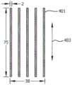
图4是在根据至少一个实施方式的示例中使用的示例性导电迹线的布置和尺寸的图示;4 is an illustration of the arrangement and dimensions of exemplary conductive traces used in an example in accordance with at least one embodiment;
图5是根据至少一个实施方式的在实施例1中测试的几种材料的应变对载荷和应变对电阻的图示。5 is a graphical representation of strain versus load and strain versus resistance for several materials tested in Example 1, according to at least one embodiment.
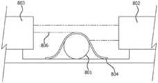
图6A是根据至少一个实施方式的具有以凹版图案以粘合点形式施加的粘合剂的基材的示意图;6A is a schematic diagram of a substrate having adhesive applied in a gravure pattern in bond spots, according to at least one embodiment;
图6B是根据至少一个实施方式的具有非导电区域的导电制品的示意图,所述非导电区域位于与吸收的导电迹线相邻的位置;6B is a schematic diagram of a conductive article having a non-conductive region located adjacent to an absorbed conductive trace in accordance with at least one embodiment;
图6C是根据至少一个实施方式的在基材的每一侧上含有印刷电路的导电制品的示意图;6C is a schematic diagram of a conductive article containing printed circuits on each side of a substrate in accordance with at least one embodiment;
图7是根据至少一个实施方式的在其中吸收有导电迹线的膨胀聚四氟乙烯膜的一部分的扫描电子显微图(SEM);7 is a scanning electron micrograph (SEM) of a portion of an expanded polytetrafluoroethylene film having conductive traces absorbed therein, according to at least one embodiment;
图8A是根据至少一个实施方式的在使用激光千分尺时,在激光千分尺源和激光千分尺接收器之间对齐的金属圆筒的示意图,该金属圆筒用于测量合成聚合物膜的厚度;和8A is a schematic diagram of a metal cylinder aligned between a laser micrometer source and a laser micrometer receiver for measuring the thickness of a synthetic polymer film when a laser micrometer is used in accordance with at least one embodiment; and
图8B是根据至少一个实施方式使用激光千分尺测量合成聚合物膜的厚度时,覆盖在图8A所示的金属圆筒的表面上的单层膜的示意图,该单层膜没有重叠且没有褶皱。Figure 8B is a schematic illustration of a monolayer film overlying the surface of the metal cylinder shown in Figure 8A, the monolayer film having no overlap and no wrinkles, using a laser micrometer to measure the thickness of the synthetic polymer film in accordance with at least one embodiment.
具体实施方式Detailed ways
本领域的技术人员应理解,可通过构造用于执行目标功能的任何数量的方法和设备来实现本公开内容的各个方面。还应注意,本文参考的附图不一定是按比例绘制,而是有可能放大以说明本公开的各个方面,就此而言,附图不应视为限制性的。应当理解,术语“导电性迹线”,“导电迹线”和“迹线”在本文中可以互换使用。术语“膜”和“薄膜”在本文中可以互换使用。如本文所用,术语“合成聚合物膜”是指包括多孔合成聚合物膜或微孔合成聚合物膜。Those skilled in the art will understand that various aspects of the present disclosure may be implemented by any number of methods and apparatus configured to perform the target functions. It should also be noted that the drawings referred to herein are not necessarily to scale, but may be exaggerated to illustrate various aspects of the present disclosure, and in this regard should not be considered limiting. It should be understood that the terms "conductive trace," "conductive trace," and "trace" are used interchangeably herein. The terms "film" and "film" are used interchangeably herein. As used herein, the term "synthetic polymer membrane" is meant to include porous synthetic polymer membranes or microporous synthetic polymer membranes.
本发明涉及包括印刷电路和可拉伸或不可拉伸基材的柔性导电制品。印刷电路包含导电迹线。可以将导电迹线吸入或以其他方式引入孔中并穿过多孔合成聚合物膜的厚度。在一些实施方式中,合成聚合物膜是微孔的。印刷电路可以不连续地结合到可拉伸或不可拉伸基材。在替代实施方式中,印刷电路连续地结合到基材。印刷电路可以集成到服装中,例如智能服装或其他可穿戴技术。The present invention relates to flexible conductive articles comprising printed circuits and stretchable or non-stretchable substrates. The printed circuit contains conductive traces. Conductive traces can be drawn or otherwise introduced into the pores and through the thickness of the porous synthetic polymer membrane. In some embodiments, the synthetic polymer membrane is microporous. Printed circuits can be discontinuously bonded to stretchable or non-stretchable substrates. In an alternative embodiment, the printed circuit is continuously bonded to the substrate. Printed circuits can be integrated into clothing, such as smart clothing or other wearable technology.
如上所述,导电制品包括印刷电路,该印刷电路包括至少一条导电迹线和多孔合成聚合物膜。如本文所用,术语“导电迹线”旨在描述能够传导电子从中通过的连续线或连续路径。在示例性实施方式中,非导电区域位于导电迹线旁边。在一些实施方式中,可使用导电油墨将导电迹线沉积在合成聚合物膜内。如本文所用,术语“导电油墨”是指在载液(例如溶剂)中掺入导电颗粒的材料。在一些实施方式中,导电颗粒包括银,金,铜或铂颗粒。合适的导电油墨的非限制性示例包括2108-IPA(Nanogap公司,加利福尼亚州里士满),UTDAgPA(UT Dots公司,伊利诺伊州香槟市),UTDAg60X(UT Dots公司,伊利诺伊州香槟市)。As mentioned above, the conductive article includes a printed circuit comprising at least one conductive trace and a porous synthetic polymer film. As used herein, the term "conductive trace" is intended to describe a continuous line or continuous path through which electrons can be conducted. In an exemplary embodiment, the non-conductive area is located next to the conductive trace. In some embodiments, conductive traces can be deposited within synthetic polymer films using conductive inks. As used herein, the term "conductive ink" refers to a material incorporating conductive particles in a carrier liquid (eg, a solvent). In some embodiments, the conductive particles include silver, gold, copper or platinum particles. Non-limiting examples of suitable conductive inks include 2108-IPA (Nanogap, Richmond, CA), UTDAgPA (UT Dots, Champaign, IL), UTDAg60X (UT Dots, Champaign, IL).
形成导电迹线的其他导电材料的非限制性示例包括导电金属颗粒或纳米颗粒(例如,银,金,铜和铂),其他导电材料(例如石墨或炭黑)的颗粒或纳米颗粒),导电纳米管,导电金属薄片,导电聚合物及其组合。如本文所用,术语“纳米颗粒”旨在描述在导电颗粒的至少一个维度上具有1.0nm至100nm的尺寸的颗粒。Non-limiting examples of other conductive materials that form conductive traces include conductive metal particles or nanoparticles (eg, silver, gold, copper, and platinum), particles or nanoparticles of other conductive materials (eg, graphite or carbon black), conductive Nanotubes, conductive metal flakes, conductive polymers, and combinations thereof. As used herein, the term "nanoparticles" is intended to describe particles having a size of 1.0 nm to 100 nm in at least one dimension of the conductive particles.
导电迹线可以呈导电图案的形式,其可以用于形成电流可以流过的电路。该图案可以创建开放路径,例如图4中例示的平行线。在一些实施方式中,电子部件(例如,表面安装电子部件)可以电耦合(例如粘附)到导电迹线图案以创建电路。在一些实施方式中,电子部件(例如,包含例如处理器、电池和/或发送器的电子模块)可以电耦合(例如粘附)到导电迹线图案以创建电路。导电迹线可以被配置为与电阻器、电容器、发光二极管(LED)、集成电路、传感器、电源以及数据发送器和接收器耦合。此外,例如,导电迹线可用于向用户或用户的医生传输信息,例如用户的心率或血液中的氧饱和度。The conductive traces can be in the form of conductive patterns, which can be used to form circuits through which electrical current can flow. This pattern can create open paths, such as parallel lines exemplified in FIG. 4 . In some embodiments, electronic components (eg, surface mount electronic components) can be electrically coupled (eg, adhered) to the conductive trace pattern to create an electrical circuit. In some embodiments, electronic components (eg, electronic modules including, for example, processors, batteries, and/or transmitters) can be electrically coupled (eg, adhered) to the conductive trace patterns to create electrical circuits. The conductive traces can be configured to couple with resistors, capacitors, light emitting diodes (LEDs), integrated circuits, sensors, power supplies, and data transmitters and receivers. Additionally, for example, the conductive traces may be used to transmit information to the user or the user's physician, such as the user's heart rate or oxygen saturation in the blood.
如上所述,导电迹线位于合成聚合物膜内。合适的多孔合成聚合物膜的非限制性示例包括膨胀聚四氟乙烯(ePTFE),聚偏二氟乙烯(PVDF),氟化乙烯丙烯(FEP),全氟烷氧基烷烃(PFA),聚酯砜(PES),如美国专利公开号2016/0032069中所述的膨胀聚对二甲苯(ePPX),如授予Sbriglia的美国专利第9,926,416号中所述的多孔膨胀超高分子量聚乙烯(eUHMWPE),如美国专利第9,932,429号中所述的多孔膨胀乙烯四氟乙烯(eETFE),如授予Sbriglia等人的美国专利第7,932,184号中所述的多孔膨胀聚乳酸(ePLLA),如授予Sbriglia的美国专利第9,441,088号中所述的多孔膨胀偏二氟乙烯-共-四氟乙烯或三氟乙烯[VDF-共-(TFE或TrFE)]聚合物及其任意组合。在至少一个实施方式中,合成聚合物膜是微孔合成聚合物膜,例如具有结点和原纤维微结构的微孔含氟聚合物膜,其中结点通过原纤维相互连接,并且孔是整个膜中位于结点和原纤维之间的空隙或空间。戈尔(Gore)的美国专利第3,953,566号中描述了示例性的结点和原纤维微结构。As mentioned above, the conductive traces are located within the synthetic polymer film. Non-limiting examples of suitable porous synthetic polymer membranes include expanded polytetrafluoroethylene (ePTFE), polyvinylidene fluoride (PVDF), fluorinated ethylene propylene (FEP), perfluoroalkoxyalkane (PFA), polyvinylidene Ester sulfone (PES), expanded parylene (ePPX) as described in US Patent Publication No. 2016/0032069, porous expanded ultra-high molecular weight polyethylene (eUHMWPE) as described in US Patent No. 9,926,416 to Sbriglia , porous expanded ethylene tetrafluoroethylene (eETFE) as described in U.S. Patent No. 9,932,429, porous expanded polylactic acid (ePLLA) as described in U.S. Patent No. 7,932,184 to Sbriglia et al. The porous expanded vinylidene fluoride-co-tetrafluoroethylene or trifluoroethylene [VDF-co-(TFE or TrFE)] polymers described in No. 9,441,088, and any combination thereof. In at least one embodiment, the synthetic polymer membrane is a microporous synthetic polymer membrane, such as a microporous fluoropolymer membrane having a microstructure of nodes and fibrils, wherein the nodes are interconnected by fibrils and the pores are throughout The voids or spaces in the membrane that lie between the junctions and the fibrils. Exemplary node and fibril microstructures are described in US Patent No. 3,953,566 to Gore.
本文所述的微孔膜可以与其他膜或结构相区别,区别在于它们的比表面积大于约4.0m2/cm3,大于约10m2/cm3,大于约50m2/cm3,大于约75m2/cm3,以及最高至100m2/cm3。在一些实施方式中,比表面积为约4.0m2/cm3至100m2/cm3。在此,比表面积是基于骨架体积而不是包络体积(envelope volume)来定义的。另外,微孔合成聚合物膜中的大多数原纤维的直径小于约1.0μm,或约0.1μm至约1.0μm,约0.3μm至约1.0μm,约0.5μm至约1.0μm,或约0.7μm至约1.0μm。另外,微孔膜很薄,厚度小于约100μm,小于约75μm,小于约50μm,小于约35μm,小于约25μm,小于约20μm,小于约10μm,小于约5μm或小于约3μm。在至少一个示例性实施方式中,合成聚合物膜是膨胀聚四氟乙烯(ePTFE)膜。根据Gore的美国专利第3,953,566号,Bowen等人的美国专利公开第2004/0173978号,Bacino等人的美国专利第7,306,729号,Bacino的美国专利第5476589号或Branca等人的美国专利第5183545号中描述的方法制备的膨胀聚四氟乙烯(ePTFE)膜也可以在本文中使用。The microporous membranes described herein can be distinguished from other membranes or structures by their specific surface area greater than about 4.0 m2 /cm3 , greater than about 10 m2 /cm3 , greater than about 50 m2 /cm3 , greater than about 75 m2 /cm3 , and up to 100m2 /cm3 . In some embodiments, the specific surface area is about 4.0 m2 /cm3 to 100 m2 /cm3 . Here, the specific surface area is defined based on the skeleton volume rather than the envelope volume. Additionally, the diameter of the majority of the fibrils in the microporous synthetic polymer film is less than about 1.0 μm, or about 0.1 μm to about 1.0 μm, about 0.3 μm to about 1.0 μm, about 0.5 μm to about 1.0 μm, or about 0.7 μm to about 1.0 μm. Additionally, the microporous membranes are thin, having a thickness of less than about 100 μm, less than about 75 μm, less than about 50 μm, less than about 35 μm, less than about 25 μm, less than about 20 μm, less than about 10 μm, less than about 5 μm, or less than about 3 μm. In at least one exemplary embodiment, the synthetic polymer membrane is an expanded polytetrafluoroethylene (ePTFE) membrane. According to US Patent No. 3,953,566 to Gore, US Patent Publication No. 2004/0173978 to Bowen et al., US Patent No. 7,306,729 to Bacino et al., US Patent No. 5,476,589 to Bacino, or US Patent No. 5,183,545 to Branca et al. Expanded polytetrafluoroethylene (ePTFE) membranes prepared by the methods described may also be used herein.
可将导电材料(例如,导电油墨)施加到多孔合成聚合物膜上,使得导电材料被吸入或以其他方式结合到多孔合成聚合物膜中,从而将导电材料,继而导电迹线设置在合成聚合物膜内,从而形成印刷电路。如本文所用,“吸收/吸入”意在描述导电迹线通过液体载体(例如导电油墨)纳入和/或沉积到多孔或微孔合成聚合物膜的现有孔或空隙中,并且特别排除了其中导电迹线是合成聚合物膜的组成部分的填充膜,其在孔或空隙空间内可能有一些暴露的导电迹线。要注意的是,在本文中可以使用填充多孔膜中的预先存在的孔或空隙空间的任何已知方法。在一些实施方式中,导电迹线在多孔或微孔合成聚合物膜的厚度上占据或填充孔。这样,导电迹线可占据多孔或微孔合成聚合物膜中的大部分孔体积。在示例性实施方式中,多孔或微孔合成聚合物膜的孔被一定量的导电材料填充,该量足以产生用于电子通过的导电迹线。可以通过已知的沉积和吸收方法将形成导电迹线的导电材料施加到多孔合成聚合物膜上,例如喷墨印刷,凹版印刷和柔版印刷,以形成导电迹线。在其中具有导电迹线的合成聚合物膜在本文中被称为印刷电路。A conductive material (eg, a conductive ink) can be applied to the porous synthetic polymer film such that the conductive material is imbibed or otherwise incorporated into the porous synthetic polymer film, thereby placing the conductive material, and then the conductive traces, on the synthetic polymer. within the film to form a printed circuit. As used herein, "absorption/imbibition" is intended to describe the incorporation and/or deposition of conductive traces by a liquid carrier (eg, conductive ink) into existing pores or voids of porous or microporous synthetic polymer membranes, and specifically excludes them The conductive traces are filled films that are components of the synthetic polymer film, which may have some exposed conductive traces within the holes or void spaces. It is noted that any known method of filling pre-existing pores or void spaces in porous membranes can be used herein. In some embodiments, the conductive traces occupy or fill pores through the thickness of the porous or microporous synthetic polymer membrane. In this way, the conductive traces can occupy most of the pore volume in the porous or microporous synthetic polymer membrane. In an exemplary embodiment, the pores of the porous or microporous synthetic polymer membrane are filled with an amount of conductive material sufficient to create conductive traces for the passage of electrons. The conductive trace-forming conductive material can be applied to the porous synthetic polymer film by known deposition and absorption methods, such as ink jet printing, gravure printing, and flexographic printing, to form the conductive traces. Synthetic polymer films having conductive traces therein are referred to herein as printed circuits.
如本文所述,导电迹线被吸入或以其他方式并入合成聚合物膜中以形成印刷电路。在至少一个实施方式中,将具有所需图案的模板施加到多孔合成聚合物膜上。应当理解,本领域技术人员已知的在合成聚合物膜上形成图案的其他形式被认为在本公开的范围内。在示例性实施方式中,在施加导电材料时,多孔合成聚合物膜是平坦的,并且不包含皱纹。可以将导电材料(例如,导电油墨)过量地施加(例如,施加过量的导电材料)在模板上,使得一旦去除模板,导电材料就以期望的图案被吸收到多孔合成聚合物膜的孔中,从而将导电材料,继而导电迹线设置在多孔合成聚合物膜内,形成印刷电路。存在于模板表面上的过量导电材料可以在去除模板之前被去除。然而,应当理解的是,由于吸收过程,可忽略量的导电材料可能残留在合成聚合物膜的表面或部分表面上。本领域已知的将导电材料结合到或吸收到多孔合成聚合物膜的孔中的其他方法也被认为在本公开的范围内。As described herein, conductive traces are imbibed or otherwise incorporated into synthetic polymer films to form printed circuits. In at least one embodiment, a template having the desired pattern is applied to the porous synthetic polymer membrane. It should be understood that other forms of patterning on synthetic polymer films known to those skilled in the art are considered to be within the scope of the present disclosure. In an exemplary embodiment, the porous synthetic polymer film is flat and does not contain wrinkles when the conductive material is applied. The conductive material (eg, conductive ink) can be applied in excess (eg, an excess of conductive material) on the template such that once the template is removed, the conductive material is absorbed into the pores of the porous synthetic polymer membrane in a desired pattern, The conductive material, and then the conductive traces, are thereby disposed within the porous synthetic polymer film to form a printed circuit. Excess conductive material present on the surface of the template can be removed prior to removal of the template. However, it should be understood that due to the absorption process, a negligible amount of conductive material may remain on the surface or part of the surface of the synthetic polymer film. Other methods known in the art to incorporate or absorb conductive materials into the pores of the porous synthetic polymer membrane are also considered to be within the scope of the present disclosure.
在形成导电制品时,可以在施加印刷电路(例如,合成聚合物膜和导电迹线)之前将不连续的粘合剂施加到基材上。印刷电路可以通过粘合剂不连续地粘附到基材上。粘合剂可以是热塑性粘合剂或热固性粘合剂。在一些实施方式中,如图6A所示,可以以凹版图案以粘合点620的形式将粘合剂施加到基材610上。应当理解,粘合剂在基材上的图案不受限制,只要基材能够在一个或多个方向上弯曲即可(例如,保持柔性)。因此,只要保持基材的柔性,其他粘合剂图案,例如网格或平行线,都被认为在本公开的范围内。如上所述,基材可以是可拉伸的或不可拉伸的。如本文所用,术语“可拉伸的”是指可以沿一个或多个方向拉动的材料(例如纺织品或织物),但是当其被释放时,该材料返回或基本上返回其原始形状。可拉伸基材可被拉伸到其松弛长度的1.25倍,1.5倍,1.7倍,2倍,3倍,4倍,5倍,6倍,7倍,8倍,9倍或10倍(或更多),具体取决于可拉伸基材的弹性。在一些实施方式中,可拉伸基材被拉伸直到达到基材的弹性极限。可以使用的可拉伸基材的实例包括但不限于可拉伸纺织品或织物,可拉伸层压件(例如,Kelsey的WO2018/067529 A1),可拉伸纤维,可拉伸非织造材料或可拉伸膜。在示例性实施方式中,印刷电路被粘合到可拉伸的纺织品或可拉伸的织物上。In forming conductive articles, the discontinuous adhesive may be applied to the substrate prior to application of the printed circuit (eg, synthetic polymer film and conductive traces). The printed circuit may be adhered to the substrate discontinuously by the adhesive. The adhesive may be a thermoplastic adhesive or a thermoset adhesive. In some embodiments, the adhesive may be applied to the
一旦基材610在其上包含粘合剂,例如粘合点620,就将包含合成聚合物膜660和导电迹线670的印刷电路650放置在基材610上方,并通过粘合点620粘附到基材610上,如图6B所示,形成导电制品600。非导电区域640定位成与吸收的导电迹线670相邻。在一些实施方式中,如图6C所示,包含导电迹线670和合成聚合物膜660的印刷电路650位于基材610的一侧上,而包含导电迹线671和合成聚合物膜661的另一印刷电路651位于相对的基材侧上。非导电区域640定位成与吸收的导电迹线670,671相邻。应当注意,合成聚合物膜670,671可以彼此相同或不同。而且,导电迹线670,671可以彼此相同或不同。图7是定位在扫描电子显微镜(SEM)安装带430上的示例性膨胀聚四氟乙烯膜410的一部分的SEM图400,该膨胀聚四氟乙烯膜410中吸收有导电迹线420。Once the
尽管未在任何图中描绘,但是应当理解,由于吸收过程,一些导电迹线可能位于多孔合成聚合物膜的表面上。在经由液体载体(例如,导电油墨)施加导电迹线的实施方式中,可以将热量施加至印刷电路以去除液体载体。施加的温度可能足以至少部分地熔化合成聚合物膜内的导电迹线(例如,金属颗粒)以形成导电颗粒的连续网络。在其他实施方式中,可以使用热量从导电颗粒中除去配体或其他加工助剂。Although not depicted in any of the figures, it should be understood that some conductive traces may be located on the surface of the porous synthetic polymer membrane due to the absorption process. In embodiments where the conductive traces are applied via a liquid carrier (eg, conductive ink), heat may be applied to the printed circuit to remove the liquid carrier. The temperature applied may be sufficient to at least partially melt the conductive traces (eg, metal particles) within the synthetic polymer film to form a continuous network of conductive particles. In other embodiments, heat can be used to remove ligands or other processing aids from the conductive particles.
在一些实施方式中,可以在导电迹线上施加绝缘外涂层,以帮助保护导电迹线不受外部因素(例如但不限于,磨损)的影响。用于使导电迹线绝缘的材料的非限制性示例包括聚氨酯(以溶液形式提供),丙烯酸类(以液体形式提供),硅酮,苯乙烯异戊二烯丁二烯嵌段共聚物,VitonTM FKM(合成橡胶和含氟聚合物弹性体),聚烯烃或含氟聚合物。In some embodiments, an insulating overcoat can be applied to the conductive traces to help protect the conductive traces from external factors such as, but not limited to, abrasion. Non-limiting examples of materials used to insulate conductive traces include polyurethane (provided in solution), acrylic (provided in liquid), silicone, styrene isoprene butadiene block copolymer, VitonTM FKM (synthetic rubber and fluoropolymer elastomer), polyolefin or fluoropolymer.
有利地,本文所述的导电制品是高度柔性的,如通过以下所述的川端测试所证明的,柔度值小于0.1克力-cm2/cm。在一些实施方式中,导电制品的柔度值小于0.009克力-cm2/cm,小于0.008克力-cm2/cm,小于0.007克力-cm2/cm,小于0.006克力-cm2/cm,小于0.005克力-cm2/cm,小于0.004克力-cm2/cm。另外,如本文所述的洗涤耐久性测试方法所证明的,吸收的多孔合成聚合物膜是高度耐用的并且能够经受多次洗涤。导电制品还具有高度透气性,其MVTR为至少2,000,如本文所述的湿蒸气透过率(MVTR)测试方法所证明的。Advantageously, the conductive articles described herein are highly flexible, as demonstrated by the Kawabata test described below, with compliance values of less than 0.1 gram force-cm2 /cm. In some embodiments, the conductive article has a compliance value of less than 0.009 gram-force-cm2 /cm, less than 0.008 gram-force-cm2 /cm, less than 0.007 gram-force-cm2 /cm, less than 0.006 gram-force-cm2 /cm cm, less than 0.005 gram-force-cm2 /cm, less than 0.004 gram-force-cm2 /cm. Additionally, the absorbent porous synthetic polymer membrane is highly durable and can withstand multiple washes as demonstrated by the Wash Durability Test Method described herein. The conductive article is also highly breathable with an MVTR of at least 2,000 as evidenced by the Moisture Vapor Transmission Rate (MVTR) test method described herein.
测试方法testing method
应理解,虽然下文描述了某些方法和设备,但也可替代性地采用本领域普通技术人员确定适用的其它方法或设备。It should be understood that while certain methods and apparatus are described below, other methods or apparatus may alternatively be employed as determined by those of ordinary skill in the art.
电阻测量与拉伸Resistance measurement and stretching
对在其上包含图4所示图案的印刷电路的屈曲纺织品进行修整,使图4所示的单条印刷导电线401可以在15mm宽的条带内居中。将条带安装在5965型

ATEQ气流ATEQ airflow
ATEQ气流测试是一种用于测量空气通过膜样品的层流体积流速的测试方法。对于各膜,以密封整个流动路径上2.99cm2面积的方式将样品夹在两块板之间。使用
格利气流Gurley Airflow
格利气流测试是测量在0.177psi(~1.22kPa)水压下100cm3空气流过1in2(~6.45cm2)样品的时间(以秒计)。在GURLEYTM透气度测定仪和4340型平滑度测定仪(格利精密仪器公司(Gurley Precision Instruments),纽约州特洛伊)中测量样品。报告的值是3次测量的平均值,以秒为单位。The Gurley airflow test measures the time (in seconds) for 100 cm3 of air to flow through a 1 in2 (-6.45 cm2 ) sample at 0.177 psi (-1.22 kPa) water pressure. Samples were measured in a GURLEY(TM) Pleometer and a Model 4340 Smoothness Tester (Gurley Precision Instruments, Troy, NY). The reported value is the average of 3 measurements in seconds.
厚度thickness
使用激光测微仪(基恩士公司(Keyence),型号LS-7010,比利时梅赫伦)测量厚度。如图8A和8B中所示,金属圆柱体801在激光测微源802和激光测微接收器803之间对齐。如图8A所示,圆柱体801的顶部的阴影805被投影到接收器803上。然后将阴影的位置重置为激光测微仪的“零”读数。如图8B所示,单层膜804被覆盖在金属圆柱体801的表面上而没有重叠并且没有褶皱,将阴影806投射到接收器803上。然后,激光测微仪将阴影805和806的位置变化指示为样品的厚度。对于每个样品,每个厚度测量三次,并取平均值。Thickness was measured using a laser micrometer (Keyence, model LS-7010, Mechelen, Belgium). As shown in FIGS. 8A and 8B , a
单位面积质量(质量/面积)Mass per unit area (mass/area)
根据ASTM D 3776(织物单位面积质量(重量)的标准测试方法(Standard TestMethods for Mass Per Unit Area(Weight)of Fabric))测试方法(选项C),使用梅特勒托利多天平(Mettler-Toledo Scale,型号1060)测量样品的单位面积质量。在对试样进行称重之前对天平进行重新校准,并且以克/平方米(g/m2)来报告结果。According to ASTM D 3776 (Standard TestMethods for Mass Per Unit Area (Weight) of Fabric) test method (option C) using a Mettler-Toledo Scale , Model 1060) to measure the mass per unit area of the sample. The balance was recalibrated before the samples were weighed, and the results were reported in grams per square meter (g/m2 ).
洗涤测试耐久性Wash Test Durability
在肯莫尔(Kenmore)洗衣机(80系列)中进行洗涤测试。负载的重量为1814.4±113.4克。水位为18±1加仑(~68.1±3.79L)。洗衣机设置为12分钟厚重棉织物洗涤(Cotton Sturdy)。洗涤温度为120±5°F(~48.9±2.78℃)。衣物洗涤剂为Original Tide粉(3700085006)。肥皂的量为11.0±0.1克。在肯莫尔(Kenmore)600烘干机中进行干燥。烘干机的设置是厚重棉织物。自动湿度感应功能设置为“正常干燥“(Normal Dry)”,并在样品干燥时结束干燥循环。一个完整的洗涤耐久性循环包括一个洗涤循环和一个干燥循环。在0、1、3、6、10、15和20个循环后,按照以下方式测量每条导电迹线的电阻:使用
湿蒸汽透过率(MVTR)测量Moisture Vapor Transmission Rate (MVTR) Measurement
将由35重量份乙酸钾和15重量份蒸馏水组成的约70ml溶液置于133mL聚丙烯杯中,该聚丙烯杯在杯口处的内径为6.5cm。用橡皮筋将膨胀聚四氟乙烯(PTFE)膜附接到该杯的口缘,产生容纳乙酸钾溶液的拉紧的防漏微孔阻挡物,该膨胀聚四氟乙烯膜根据Crosby的美国专利第4,862,730号描述的方法测试的最小MVTR约为85,000g/m2/24小时。About 70 ml of a solution consisting of 35 parts by weight of potassium acetate and 15 parts by weight of distilled water was placed in a 133 mL polypropylene cup with an inner diameter of 6.5 cm at the mouth of the cup. An expanded polytetrafluoroethylene (PTFE) membrane according to Crosby's U.S. Patent was attached with a rubber band to the lip of the cup, creating a taut, leak-proof microporous barrier containing the potassium acetate solution The minimum MVTR tested by the method described in No. 4,862,730 was approximately 85,000 g/m2 /24 hours.
将类似的膨胀PTFE膜安装在水浴的表面。使用控温室和水循环浴将水浴组件控制在23±0.2℃。A similar expanded PTFE membrane was mounted on the surface of the water bath. Control the water bath assembly at 23 ± 0.2°C using a controlled chamber and a water circulating bath.
进行该测试过程前,使待测试样品在23℃的温度和50%的相对湿度下调理。放置样品,使导电迹线背向安装到水浴表面的膨胀聚四氟乙烯膜,并平衡至少15分钟,然后将杯组件引入。杯组件称重至精确度1/1000g,并以倒置的方式放置在测试样品的中心上。The samples to be tested were conditioned at a temperature of 23°C and a relative humidity of 50% prior to the testing procedure. The sample was placed with the conductive traces facing away from the expanded Teflon membrane mounted to the surface of the water bath and equilibrated for at least 15 minutes before the cup assembly was introduced. The cup assembly is weighed to an accuracy of 1/1000 g and placed upside down on the center of the test sample.
通过水浴中水和饱和盐溶液之间的驱动力提供水传输,所述饱和盐溶液通过在该方向上的扩散来提供水通量。对样品测试15分钟,随后移开杯组件,再次称量至1/1000g精确度。Water transport is provided by the driving force between the water in the water bath and the saturated salt solution which provides the water flux by diffusion in this direction. The samples were tested for 15 minutes, after which time the cup assembly was removed and weighed again to an accuracy of 1/1000 g.
由杯组件的重量增加计算样品的MVTR,并表示为每24小时每平方米样品表面积的水克数。The MVTR of the sample was calculated from the weight gain of the cup assembly and expressed as grams of water per square meter of sample surface area per 24 hours.
基质拉伸强度测定Substrate Tensile Strength Determination
使用ASTM D412-Dogbone F在每个纵向和横向方向上切割合成聚合物膜。“纵向”为挤出方向,“横向”与其垂直。将膜放置在切割台上,使得膜在要切割膜的区域中没有褶皱。然后,将模具放置在膜上(通常在膜中心200mm范围内),使其长轴平行于要测试的方向。模具对齐之后,施加压力以切穿合成聚合物膜。去除压力后,检查犬骨状样品,以确保其没有可能影响拉伸测试的边缘缺陷。以这种方式制备了至少3个纵向样品和3个横向样品。一旦制备了犬骨状样品,就使用梅特勒-托利多(Mettler Toledo)天平(型号AG204)对其进行测量以确定其质量。Synthetic polymer films were cut in each machine and cross direction using ASTM D412-Dogbone F. "Longitudinal" is the extrusion direction, and "transverse" is perpendicular to it. Place the film on the cutting table so that the film is free of wrinkles in the area where the film is to be cut. The mold is then placed on the film (usually within 200mm of the center of the film) with its long axis parallel to the direction to be tested. After the molds are aligned, pressure is applied to cut through the synthetic polymer film. After the pressure was removed, the canine bone sample was inspected to ensure that it had no edge defects that could affect the tensile test. At least 3 longitudinal samples and 3 transverse samples were prepared in this way. Once the canine bone sample was prepared, it was measured using a Mettler Toledo balance (model AG204) to determine its mass.
使用配备有橡胶涂覆的面板和锯齿状面板的
以下公式用于计算基质拉伸强度:The following formula is used to calculate the matrix tensile strength:
MTS=((F最大/w)*p)/质量:面积,其中:MTS=((Fmax /w)*p)/mass:area, where:
MTS=基质拉伸强度,MPa,MTS = matrix tensile strength, MPa,
F最大=测试中测量的最大载荷(牛顿),Fmax =maximum load (in Newtons) measured in the test,
w=标距长度内的犬骨状样品的宽度(米),w = width (m) of the canine bone sample within the gauge length,
p=PTFE的密度(2.2x10⁶g/m3)或聚乙烯的密度(0.94g/m3),以及p = density of PTFE (2.2x10⁶ g/m3 ) or density of polyethylene (0.94 g/m3 ), and
质量:面积=样品单位面积质量(g/m2)。Mass: area = mass per unit area of sample (g/m2 ).
川端柔性测量Kawabata Flexible Measurement
使用川端纯弯曲测试仪(KES-FB2-Auto-A;加藤科技有限公司(Kato TechCo.LTD),日本京都)测量层压样品的低力弯曲行为。将层压样品切成7cm的宽度,使印刷图案大致居中,并且印刷线垂直于7cm的宽度延伸。将样品放置在弯曲测试仪的夹具内,使印刷线跨过夹具之间的间隙。机器灵敏度设定为10。在记录施加的载荷的同时,机器自动拧紧夹具并将层压样品在两个方向上弯曲成2.5cm-1的曲率。报道的B均值是层压样品在0.5至1.5cm-1和-0.5至-1.5cm-1之间弯曲时的弯曲刚度的平均值。弯曲刚度以克力cm2/cm表示。The low-force bending behavior of the laminated samples was measured using a Kawabata Pure Bend Tester (KES-FB2-Auto-A; Kato TechCo. LTD, Kyoto, Japan). The laminate samples were cut to a width of 7 cm with the print pattern approximately centered and the print lines extending perpendicular to the width of 7 cm. Place the sample in the clamps of the bend tester so that the printed line spans the gap between the clamps. The machine sensitivity is set to 10. While recording the applied load, the machine automatically tightened the clamps and bent the laminated sample to a curvature of 2.5 cm-1 in both directions. The reported B-means are the average values of the flexural stiffness of the laminated samples when bent between 0.5 to 1.5 cm"1 and -0.5 to -1.5 cm"1 . Bending stiffness is expressed in grams force cm2 /cm.
泡点bubble point
使用毛细流动气孔计(型号3Gzh,来自美国佛罗里达州博因顿海滩市的康塔仪器公司(Quantachrome Instruments,Boynton Beach,Florida)),根据ASTM F31 6-03的一般教导测量泡点压力。将样品膜放置于样品室中,用表面张力为20.1达因/厘米的SilWick硅酮流体(Silwick Silicone Fluid)(购自多孔材料公司(Porous Materials Inc.))润湿。样品室的底部夹具直径为2.54cm,具有0.159cm厚的多孔金属圆盘插入件(康塔零件号75461不锈钢过滤器),用于支撑样品。使用2.1版的3GWin软件,按紧跟着的下表所示设定以下参数。表示泡点压力的值取两次测量的平均值。使用以下公式将泡点压力转换为孔径:Bubble point pressure was measured using a capillary flow porosimeter (Model 3Gzh from Quantachrome Instruments, Boynton Beach, Florida, USA) according to the general teachings of ASTM F31 6-03. The sample membrane was placed in the sample chamber and wetted with Silwick Silicone Fluid (available from Porous Materials Inc.) with a surface tension of 20.1 dynes/cm. The bottom clamp of the sample chamber was 2.54 cm in diameter with a 0.159 cm thick porous metal disc insert (Canta Part No. 75461 stainless steel filter) to support the sample. Using 3GWin software version 2.1, set the following parameters as shown in the table immediately following. The value representing the bubble point pressure is taken as the average of two measurements. Convert bubble point pressure to pore size using the following formula:
DBP=4γlvcosθ/PBPDBP=4γlvcosθ/PBP
其中DBP是孔径,γlv是液体表面张力,θ是流体在材料表面上的接触角,PBP是泡点压力。本领域技术人员应理解,在泡点测量中使用的流体必须润湿样品的表面。where DBP is the pore size, γlv is the liquid surface tension, θ is the contact angle of the fluid on the material surface, and PBP is the bubble point pressure. It will be understood by those skilled in the art that the fluid used in bubble point measurements must wet the surface of the sample.
泡点仪器设定Bubble Point Instrument Settings


ePTFE膜ePTFE membrane
ePTFE膜1–制备ePTFE膜
根据Bowen等人的美国专利公开号2004/0173978中提出的一般教导来制造ePTFE膜。ePTFE膜的单位面积质量为4.6g/m2,孔隙率为87%,非接触厚度为15.5μm,格利(Gurley)数为4.5秒,在12毫巴下的ATEQ空气流量为17升/cm2/小时,纵向的基质拉伸强度为258MPa,横向的基质拉伸强度为329MPa,比表面积为14.520m2/g,单位体积的表面积为31.944m2/cm3。ePTFE膜的扫描电子显微镜(SEM)图像显示在图1中。The ePTFE membranes were fabricated according to the general teachings set forth in US Patent Publication No. 2004/0173978 to Bowen et al. The mass per unit area of the ePTFE membrane is 4.6 g/m2 , the porosity is 87%, the non-contact thickness is 15.5 μm, the Gurley number is 4.5 seconds, and the ATEQ air flow at 12 mbar is 17 liters/cm2 /hour, the tensile strength of the matrix in the longitudinal direction was 258 MPa, the tensile strength of the matrix in the transverse direction was 329 MPa, the specific surface area was 14.520 m2 /g, and the surface area per unit volume was 31.944 m2 /cm3 . A scanning electron microscope (SEM) image of the ePTFE membrane is shown in FIG. 1 .
ePTFE膜2–制备ePTFE膜
根据上述戈尔的美国专利第3,953,566号中阐述的一般教导来制造ePTFE膜。ePTFE膜的单位面积质量为16.6g/m2,孔隙率为80%,非接触厚度为37.6μm,泡点为156kPa,纵向的基质拉伸强度为42.4MPa,横向的基质拉伸强度为116.4MPa,比表面积为7.891m2/g,单位体积的表面积为17.75m2/cm3。图2显示了ePTFE膜的SEM图像。The ePTFE membranes were fabricated according to the general teachings set forth in the aforementioned Gore US Patent No. 3,953,566. The mass per unit area of the ePTFE membrane is 16.6 g/m2 , the porosity is 80%, the non-contact thickness is 37.6 μm, the bubble point is 156 kPa, the tensile strength of the matrix in the longitudinal direction is 42.4 MPa, and the tensile strength of the matrix in the transverse direction is 116.4 MPa. , the specific surface area is 7.891m2 /g, and the surface area per unit volume is 17.75m2 /cm3 . Figure 2 shows the SEM image of the ePTFE membrane.
实施例Example
上文中已经概括性地并且结合具体实施方式描述了本申请的发明。对本领域的技术人员来说显而易见的是,可以在不偏离本公开的范围的情况下,对实施方式进行各种修改和变动。因此,实施方式旨在覆盖对本发明的这些修改和变动,只要这些修改和变动在所附权利要求及其等同方案的范围之内。The invention of the present application has been described above both generally and in conjunction with specific embodiments. It will be apparent to those skilled in the art that various modifications and variations can be made in the embodiments without departing from the scope of the present disclosure. Accordingly, the embodiments are intended to cover such modifications and variations of this invention as come within the scope of the appended claims and their equivalents.
实施例1Example 1
膨胀聚四氟乙烯(ePTFE)(膜1)用作吸收的基材。将ePTFE膜放在直径6英寸(~15.24cm)的铝制箍上,通过在圆周上放置不锈钢弹簧将其固定到箍上,并用手张紧基材以去除皱纹,由此约束ePTFE膜。为了在模板附着期间支撑ePTFE膜,将约束ePTFE膜的箍放在干净的
为了制备模板,将一块胶带(Scapa 536型;聚酯膜,单面涂有丙烯酸类粘合剂;斯卡帕北美公司(Scapa North America),康涅狄格州温莎)转移到离型纸上。使用激光切割机(PLS6.75激光切割机,通用激光公司(Universal Laser),亚利桑那州斯科茨代尔)在胶带中切出孔,以形成图4所示的图案。图4提供的尺寸以毫米(mm)为单位,表示所施加的图案的尺寸。示出了双向箭头402以说明拉伸织物与柔性电路的对齐。然后将胶带模板从离型纸上取下,并用手将其压在ePTFE膜的暴露“顶”表面的表面上,以将模板牢固地粘附到ePTFE膜上。然后将仍约束在箍上的模板和ePTFE膜从
导电油墨的吸收Absorption of conductive ink
通过模板中的孔将过量的导电油墨(2108-IPA;包括稳定分散的银纳米颗粒的油墨制剂,可从加利福尼亚州里士满的Nanogap公司获得)吸移到ePTFE膜的顶表面上。该过程完成后,用单层纤维素擦拭纸巾(Delicate Task擦拭纸巾;
将粘合点粘合到拉伸纺织品Bonding Bond Points to Stretch Textiles
使用18Q236凹版印刷图案将UT聚氨酯热塑性粘合剂(Protechnic公司,法国塞尔内)印刷到离型纸上。将尼龙/聚酯/弹性纤维混纺、斜纹编织、经向拉伸纺织品(TD36B,中国台湾台北市台湾化学纤维股份有限公司(Formosa Chemicals and Fibre Corporation))在经向拉伸至其松弛长度的2倍左右,并约束在矩形框架中。将一块112mm x 152mm的聚氨酯粘合剂印刷的离型纸放置在纺织品上,并通过在135℃的T恤压机中将其压制约5秒来将其热层压到纺织品上。冷却后,将离型纸移走,留下粘合到拉伸纺织品上的聚氨酯粘合点。A UT polyurethane thermoplastic adhesive (Protechnic, Cernay, France) was printed onto release paper using an 18Q236 gravure pattern. Nylon/polyester/elastane blended, twill weave, warp stretched textiles (TD36B, Formosa Chemicals and Fibre Corporation, Taipei, Taiwan, China) were stretched in the warp direction to 2 of their relaxed lengths. times, and constrained in a rectangular frame. A piece of 112mm x 152mm polyurethane adhesive printed release liner was placed on the textile and heat laminated to the textile by pressing it in a T-shirt press at 135°C for about 5 seconds. After cooling, the release liner was removed, leaving the polyurethane bond points bonded to the stretched textile.
制备结构化(“屈曲的”)层压件Preparation of structured ("buckled") laminates
将具有吸收的导电迹线(即印刷电路)的ePTFE膜修整为128mm x 78mm,使印刷图案大致居中。然后将印刷电路居中在粘合到纺织品上的粘合点的顶部上,使图4中的箭头402与纺织品的经向对齐。然后通过将印刷电路在T恤压机中于135℃压制约5秒来将其热层压到纺织品上。冷却后,将纺织品从框架中释放出来,并使其恢复到松弛状态,从而使印刷电路随纺织品(导电制品)压缩并屈曲。The ePTFE film with the absorbed conductive traces (ie the printed circuit) was trimmed to 128mm x 78mm with the printed pattern approximately centered. The printed circuit is then centered on top of the bond points bonded to the textile, aligning
电阻测量与拉伸Resistance measurement and stretching
如上述测试方法中所述进行电阻测量与拉伸的测试。该电阻测试的结果在图5和表1中示出。不连续曲线501示出了未层压的纺织品的载荷-应变关系,而连续曲线502示出了当各样品被拉伸至50%应变并返回至0%应变时的柔性制品的载荷-应变关系。两者都在主y轴上读取。圆形标记503显示层压样品的导电迹线相对于应变的欧姆电阻,并在次y轴上读取。经测定,当柔性电路被拉长到50%应变时,印刷电路的电阻基本上保持不变。Resistance measurements and tensile tests were performed as described in the test methods above. The results of this resistance test are shown in Figure 5 and Table 1.
洗涤测试washing test
如上文所述的测试方法中所述进行洗涤耐久性测试。在50%的迹线超过1兆欧(MΩ)之前,确定印刷电路可以经受至少20次的洗涤循环。The wash durability test was performed as described in the test methods described above. The printed circuit was determined to withstand at least 20 wash cycles before 50% of the traces exceeded 1 megohm (MΩ).
MTVRMTVR
如上述测试方法中所述测量湿蒸气透过率。测得的MVTR为15680g/m2/24小时(表1)。Moisture Vapor Transmission Rate was measured as described in the above test method. The measured MVTR was 15680 g/m2 /24 hours (Table 1).
川端测试Kawabata Test
如上文所述的测试方法中所述进行川端弯曲测试。测量的川端弯曲测试值为0.0418克力-cm2/cm。The Kawabata bend test was performed as described in the test methods described above. The measured Kawabata Bend Test value was 0.0418 gram force-cm2 /cm.
实施例2Example 2
膨胀聚四氟乙烯(ePTFE)(膜1)用作印刷的基材。将ePTFE膜限制在直径为356mm的绣花箍中,张紧以去除皱纹,并使用导电油墨以图4所示的图案进行丝网印刷。图4所示的尺寸以mm为单位,表示所施加的图案的尺寸。示出了双向箭头402以说明基材与柔性电路的对齐。使用型号MSP-088的丝网印刷机(新泽西州黎巴嫩市的HMI制造公司)进行丝网印刷,其中不锈钢丝网具有200TPI(每英寸的纱/线;~78.74线/cm),1.6密耳(~40.64μm)线直径,和12.7μm的乳液。所用的导电油墨为CI1036(高导电性银油墨;总固体含量为66%;工程导电材料公司,俄亥俄州特拉华)。将油墨在对流烘箱中于120℃下干燥20分钟。通过将基材修整至128mm x 78mm,使印刷图案大致居中位于ePTFE膜上,从而将印刷电路从绣花箍上取下。将聚氨酯粘合点粘合到拉伸纺织品上的过程遵循实施例1中所述的过程。该拉伸纺织品与实施例1中所用的相同。Expanded polytetrafluoroethylene (ePTFE) (film 1) was used as the substrate for printing. The ePTFE membrane was confined in a 356mm diameter embroidery hoop, tensioned to remove wrinkles, and screen printed using conductive ink in the pattern shown in Figure 4. The dimensions shown in Figure 4 are in mm and represent the dimensions of the applied pattern. A double-headed
按照实施例1中所述的方法制备结构化(“屈曲的”)ePTFE层压件,以将印刷电路粘附至拉伸纺织品(例如,导电制品)。Structured ("flexed") ePTFE laminates were prepared as described in Example 1 to adhere printed circuits to stretched textiles (eg, conductive articles).
电阻测量与拉伸Resistance measurement and stretching
如上述测试方法中所述进行电阻测量与拉伸的测试。当柔性电路被拉长到50%应变时,电路的电阻基本上保持不变。Resistance measurements and tensile tests were performed as described in the test methods above. When the flex circuit was stretched to 50% strain, the resistance of the circuit remained essentially unchanged.
洗涤测试washing test
如上文所述的测试方法中所述进行洗涤耐久性测试。在50%的迹线超过1兆欧(MΩ)之前,确定印刷电路可以经受3次洗涤循环(表1)。The wash durability test was performed as described in the test methods described above. The printed circuit was determined to withstand 3 wash cycles before 50% of the traces exceeded 1 megohm (MΩ) (Table 1).
MTVRMTVR
如上述测试方法中所述测量柔性电路的湿蒸气透过率。测得的MVTR为16085g/m2/24小时(表1)。The moisture vapor transmission rate of the flexible circuit was measured as described in the test method above. The measured MVTR was 16085 g/m2 /24 hours (Table 1).
川端测试Kawabata Test
如上文所述的测试方法中所述进行川端弯曲测试。测量的川端弯曲测试值为0.0364克力-cm2/cm。The Kawabata bend test was performed as described in the test methods described above. The measured Kawabata Bend Test value was 0.0364 gram force-cm2 /cm.
实施例3Example 3
膨胀聚四氟乙烯(ePTFE)(膜2)用作印刷的基材。将ePTFE膜限制在直径为356mm的绣花箍中,张紧以去除皱纹,并使用导电油墨以图4所示的图案进行丝网印刷。图4所示的尺寸以mm为单位,仅供参考,表示所施加的图案的尺寸。示出了双向箭头402以说明基材与柔性电路的对齐。使用型号MSP-088的丝网印刷机(新泽西州黎巴嫩市的HMI制造公司)进行丝网印刷,其中不锈钢丝网具有200TPI(每英寸的纱/线;~78.74线/cm),1.6密耳(~40.64μm)线直径,和12.7μm的乳液。所用的导电油墨为CI1036(高导电性银油墨;总固体含量为66%;工程导电材料公司,俄亥俄州特拉华)。将油墨在对流烘箱中于120℃下干燥20分钟。通过将基材修整至128mm x 78mm,使印刷图案大致居中位于ePTFE膜上,从而将印刷的ePTFE膜从绣花箍上取下。Expanded polytetrafluoroethylene (ePTFE) (membrane 2) was used as the substrate for printing. The ePTFE membrane was confined in a 356mm diameter embroidery hoop, tensioned to remove wrinkles, and screen printed using conductive ink in the pattern shown in Figure 4. The dimensions shown in Figure 4 are in mm for reference only and represent the dimensions of the applied pattern. A double-headed
将粘合点粘合到拉伸纺织品上的过程遵循实施例1中所述的过程。该纺织品与实施例1中所用的相同。The procedure for bonding the bond points to the stretched textile followed the procedure described in Example 1. The textile is the same as used in Example 1.
按照实施例1中所述的方法制备结构化(“屈曲的”)ePTFE层压件,以将柔性电路粘附至拉伸纺织品。Structured ("flexed") ePTFE laminates were prepared as described in Example 1 to adhere flexible circuits to stretched textiles.
电阻测量与拉伸Resistance measurement and stretching
如上述测试方法中所述进行电阻测量与拉伸的测试。当柔性电路被拉长到50%应变时,电路的电阻基本上保持不变。Resistance measurements and tensile tests were performed as described in the test methods above. When the flex circuit was stretched to 50% strain, the resistance of the circuit remained essentially unchanged.
洗涤测试washing test
如上文所述的测试方法中所述进行洗涤耐久性测试。在50%的迹线超过1兆欧(MΩ)之前,确定印刷电路可以经受3次洗涤循环(表1)。The wash durability test was performed as described in the test methods described above. The printed circuit was determined to withstand 3 wash cycles before 50% of the traces exceeded 1 megohm (MΩ) (Table 1).
MTVRMTVR
如上述测试方法中所述测量柔性电路的湿蒸气透过率。测得的MVTR为14263g/m2/24小时(表1)。The moisture vapor transmission rate of the flexible circuit was measured as described in the test method above. The measured MVTR was 14263 g/m2 /24 hours (Table 1).
川端测试Kawabata Test
如上文所述的测试方法中所述进行川端弯曲测试。测量的川端弯曲测试值为0.0348克力-cm2/cm。The Kawabata bend test was performed as described in the test methods described above. The measured Kawabata Bend Test value was 0.0348 gram force-cm2 /cm.
实施例4Example 4
获得了市售的25μm厚的热塑性聚氨酯膜(TPU),
使用型号MSP-088的丝网印刷机(新泽西州黎巴嫩市的HMI制造公司)进行丝网印刷,其中不锈钢丝网具有200TPI(每英寸的纱/线;~78.74线/cm),1.6密耳(~40.64μm)线直径,和12.7μm的乳液。所用的导电油墨为CI1036(高导电性银油墨;总固体含量为66%;工程导电材料公司,俄亥俄州特拉华)。将油墨在对流烘箱中于120℃下干燥20分钟。通过将基材修整至128mm x 78mm,使印刷图案大致居中位于UTP膜上,从而将印刷的基材从绣花箍上取下。Screen printing was performed using a model MSP-088 screen printer (HMI Manufacturing, Lebanon, NJ) with a stainless steel screen having 200 TPI (yarns per inch; ~78.74 threads/cm), 1.6 mil ( ~40.64 μm) wire diameter, and a 12.7 μm emulsion. The conductive ink used was CI1036 (high conductive silver ink; 66% total solids; Engineered Conductive Materials, Delaware, OH). The ink was dried in a convection oven at 120°C for 20 minutes. Remove the printed substrate from the embroidery hoop by trimming the substrate to 128mm x 78mm so that the printed pattern is approximately centered on the UTP film.
将粘合点粘合到拉伸纺织品上的过程遵循实施例1中所述的过程。该纺织品与实施例1中的相同。The procedure for bonding the bond points to the stretched textile followed the procedure described in Example 1. The textile is the same as in Example 1.
按照实施例1中所述的方法制备结构化(“屈曲的”)层压件,以将柔性电路粘附至拉伸纺织品。Structured ("flexed") laminates were prepared as described in Example 1 to adhere flexible circuits to stretch textiles.
电阻测量与拉伸Resistance measurement and stretching
如上述测试方法中所述进行电阻测量与拉伸的测试。当柔性电路被拉长到50%应变时,电路的电阻基本上保持不变。Resistance measurements and tensile tests were performed as described in the test methods above. When the flex circuit was stretched to 50% strain, the resistance of the circuit remained essentially unchanged.
洗涤测试washing test
如上文所述的测试方法中所述进行洗涤耐久性测试。在50%的迹线超过1兆欧(MΩ)之前,确定印刷电路可以经受1次洗涤循环(表1)。The wash durability test was performed as described in the test methods described above. The printed circuit was determined to survive 1 wash cycle before 50% of the traces exceeded 1 megohm (MΩ) (Table 1).
MTVRMTVR
如上述测试方法中所述测量柔性电路的湿蒸气透过率。测得的MVTR为2459g/m2/24小时(表1)。The moisture vapor transmission rate of the flexible circuit was measured as described in the test method above. The measured MVTR was 2459 g/m2 /24 hours (Table 1).
川端测试Kawabata Test
如上文所述的测试方法中所述进行川端弯曲测试。测量的川端弯曲测试值为0.0527克力-cm2/cm。The Kawabata bend test was performed as described in the test methods described above. The measured Kawabata Bend Test value was 0.0527 gram force-cm2 /cm.
实施例5Example 5
获得了厚度为12μm的多孔聚乙烯锂离子电池隔离件(T3,派尔材料有限公司(PairMaterials Co.Ltd),中国东莞)。该聚乙烯膜的单位面积质量为7.0g/m2,孔隙率为40%,厚度为12.4μm,泡点为1543kPa,纵向的基质拉伸强度为314MPa,横向的基质拉伸强度为233MPa,比表面积为34.1m2/g,单位体积的表面积为32.1m2/cm3。图3显示了该聚乙烯膜的SEM图像。A porous polyethylene lithium-ion battery separator (T3, Pair Materials Co. Ltd, Dongguan, China) with a thickness of 12 μm was obtained. The mass per unit area of the polyethylene film is 7.0 g/m2 , the porosity is 40%, the thickness is 12.4 μm, the bubble point is 1543 kPa, the tensile strength of the matrix in the longitudinal direction is 314 MPa, and the tensile strength of the matrix in the transverse direction is 233 MPa. The surface area was 34.1 m2 /g, and the surface area per unit volume was 32.1 m2 /cm3 . Figure 3 shows an SEM image of the polyethylene film.
将聚乙烯膜约束在直径为356mm的绣花箍中,张紧以去除皱纹,并使用导电油墨以图4所示的图案进行丝网印刷。图4所示的尺寸以mm为单位,仅供参考,表示所施加的图案的尺寸。图4中示出了双向箭头402,以说明基材与柔性电路的对齐。使用型号MSP-088的丝网印刷机(新泽西州黎巴嫩市的HMI制造公司)进行丝网印刷,其中不锈钢丝网具有200TPI(每英寸的螺纹/线;~78.74线/cm),1.6密耳(~40.64μm)线直径,和12.7μm的乳液。所用的导电油墨为CI1036(高导电性银油墨;总固体含量为66%;工程导电材料公司,俄亥俄州特拉华)。将油墨在对流烘箱中于120℃下干燥20分钟。通过将聚乙烯膜修整至128mm x 78mm,使印刷图案大致居中位于聚乙烯膜上(印刷电路),从而将印刷的聚乙烯膜从绣花箍上取下。The polyethylene film was restrained in a 356mm diameter embroidery hoop, tensioned to remove wrinkles, and screen printed using conductive ink in the pattern shown in Figure 4. The dimensions shown in Figure 4 are in mm for reference only and represent the dimensions of the applied pattern. A
将粘合点粘合到拉伸纺织品上的过程遵循实施例1中所述的过程。该纺织品与实施例1中所用的相同。The procedure for bonding the bond points to the stretched textile followed the procedure described in Example 1. The textile is the same as used in Example 1.
按照实施例1中所述的方法制备结构化(“屈曲的”)层压件,以将柔性电路粘附至拉伸纺织品。Structured ("flexed") laminates were prepared as described in Example 1 to adhere flexible circuits to stretch textiles.
电阻测量与拉伸Resistance measurement and stretching
如上述测试方法中所述进行电阻测量与拉伸的测试。当柔性电路被拉长到50%应变时,电路的电阻基本上保持不变。Resistance measurements and tensile tests were performed as described in the test methods above. When the flex circuit was stretched to 50% strain, the resistance of the circuit remained essentially unchanged.
洗涤测试washing test
如上文所述的测试方法中所述进行洗涤耐久性测试。在50%的迹线超过1兆欧(MΩ)之前,确定印刷电路可以经受3次洗涤循环(表1)。The wash durability test was performed as described in the test methods described above. The printed circuit was determined to withstand 3 wash cycles before 50% of the traces exceeded 1 megohm (MΩ) (Table 1).
MTVRMTVR
如上述测试方法中所述测量柔性电路的湿蒸气透过率。测得的MVTR为9721g/m2/24小时(表1)。The moisture vapor transmission rate of the flexible circuit was measured as described in the test method above. The measured MVTR was 9721 g/m2 /24 hours (Table 1).
川端测试Kawabata Test
如上文所述的测试方法中所述进行川端弯曲测试。测量的川端弯曲测试值为0.0970克力-cm2/cm。The Kawabata bend test was performed as described in the test methods described above. The measured Kawabata Bend Test value was 0.0970 gram force-cm2 /cm.
实施例6Example 6
膨胀聚四氟乙烯(ePTFE)膜(膜1)用作基材。为了制备用于吸收的ePTFE膜,将ePTFE膜放在直径6英寸的铝制箍上,通过在圆周上放置不锈钢弹簧将其固定到箍上,并张紧ePTFE膜以去除皱纹,由此约束ePTFE膜。为了在模板附着期间支撑ePTFE膜,将约束ePTFE膜的箍放在干净的
然后将胶带模板从离型纸上取下,并用手将其压在ePTFE膜的暴露“顶”表面的表面上,以将模板牢固地粘附到ePTFE膜上。然后将仍约束在箍上的模板和ePTFE膜从
使用18Q236凹版印刷图案将UT聚氨酯热塑性粘合剂(Protechnic公司,法国塞尔内)印刷到离型纸上。将尼龙/聚酯/弹性纤维混纺、斜纹编织、经向拉伸纺织品(TD36B,中国台湾台北市台湾化学纤维股份有限公司)约束在矩形框架中,其中织物为非拉伸(松弛)状态。将一块112mm x 152mm的粘合剂印刷的离型纸放置在纺织品上,并通过在T恤压机中于135℃下将离型纸和纺织品压制约5秒来将该离型纸热层压到纺织品上。冷却后,将离型纸移走,留下粘合到纺织品上的粘合点。为了将印刷电路粘附到纺织品上,首先将印刷电路修整为128mm×78mm,使印刷图案大致居中位于粘合到纺织品的粘合点上,使图4中的箭头402与纺织品的经向对齐。然后通过将含有印刷电路的纺织品在T恤压机中于135℃压制约5秒来将印刷电路热层压到纺织品上。冷却后,将纺织品从框架中释放出来。A UT polyurethane thermoplastic adhesive (Protechnic, Cernay, France) was printed onto release paper using an 18Q236 gravure pattern. A nylon/polyester/elastane blend, twill weave, warp stretched textile (TD36B, Taiwan Chemical Fiber Co., Ltd., Taipei, Taiwan, China) was constrained in a rectangular frame with the fabric in an unstretched (relaxed) state. A piece of 112mm x 152mm adhesive printed release liner was placed on the textile and thermally laminated by pressing the release paper and the textile in a T-shirt press at 135°C for about 5 seconds to textiles. After cooling, the release liner is removed, leaving bond points to the textile. To adhere the printed circuit to the textile, the printed circuit was first trimmed to 128mm x 78mm with the printed pattern approximately centered on the bond point to the textile, aligning
电阻测量与拉伸Resistance measurement and stretching
如上述测试方法中所述进行电阻测量与拉伸的测试。当柔性电路被拉长到50%应变时,印刷电路的电阻明显增加。Resistance measurements and tensile tests were performed as described in the test methods above. When the flex circuit was stretched to 50% strain, the resistance of the printed circuit increased significantly.
洗涤测试washing test
如上文所述的测试方法中所述进行洗涤耐久性测试。在50%的迹线超过1兆欧(MΩ)之前,确定样品可以经受6次洗涤循环(表1)。The wash durability test was performed as described in the test methods described above. The samples were determined to withstand 6 wash cycles before 50% of the traces exceeded 1 megohm (MΩ) (Table 1).
MTVRMTVR
如上述测试方法中所述测量柔性电路的湿蒸气透过率。测得的MVTR为17127g/m2/24小时(表1)。The moisture vapor transmission rate of the flexible circuit was measured as described in the test method above. The measured MVTR was 17127 g/m2 /24 hours (Table 1).
川端测试Kawabata Test
如上文所述的测试方法中所述进行川端弯曲测试。测量的川端弯曲测试值为0.0669克力-cm2/cm。The Kawabata bend test was performed as described in the test methods described above. The measured Kawabata Bend Test value was 0.0669 gram force-cm2 /cm.
实施例7Example 7
膨胀聚四氟乙烯(ePTFE)膜(膜1)用作基材。将ePTFE膜限制在直径为356mm的绣花箍中,张紧以去除皱纹,并使用导电油墨以图4所示的图案进行丝网印刷。图4所示的尺寸以mm为单位,仅供参考,表示所施加的图案的尺寸。使用型号MSP-088的丝网印刷机(新泽西州黎巴嫩市的HMI制造公司)进行丝网印刷,其中不锈钢丝网具有200TPI(每英寸的纱/线;~78.74线/cm),1.6密耳(~40.64μm)线直径,和12.7μm的乳液。所用的导电油墨为CI1036(高导电性银油墨;总固体含量为66%;工程导电材料公司,俄亥俄州特拉华)。将油墨在对流烘箱中于120℃下干燥20分钟。通过将ePTFE膜修整至128mm x 78mm,使印刷图案大致居中位于ePTFE膜上,从而将印刷的ePTFE膜从绣花箍上取下。An expanded polytetrafluoroethylene (ePTFE) membrane (membrane 1) was used as the substrate. The ePTFE membrane was confined in a 356mm diameter embroidery hoop, tensioned to remove wrinkles, and screen printed using conductive ink in the pattern shown in Figure 4. The dimensions shown in Figure 4 are in mm for reference only and represent the dimensions of the applied pattern. Screen printing was performed using a model MSP-088 screen printer (HMI Manufacturing, Lebanon, NJ) with a stainless steel screen having 200 TPI (yarns per inch; ~78.74 threads/cm), 1.6 mil ( ~40.64 μm) wire diameter, and a 12.7 μm emulsion. The conductive ink used was CI1036 (high conductive silver ink; 66% total solids; Engineered Conductive Materials, Delaware, OH). The ink was dried in a convection oven at 120°C for 20 minutes. The printed ePTFE membrane was removed from the embroidery hoop by trimming the ePTFE membrane to 128mm x 78mm so that the printed pattern was approximately centered on the ePTFE membrane.
使用18Q236凹版印刷图案将UT聚氨酯热塑性粘合剂(Protechnic公司,法国塞尔内)印刷到离型纸上。将尼龙/聚酯/弹性纤维混纺、斜纹编织、经向拉伸纺织品(TD36B,中国台湾台北市台湾化学纤维股份有限公司)约束在矩形框架中,其中织物为非拉伸(松弛)状态。将一块112mm x 152mm的粘合剂印刷的离型纸放置在纺织品上,并通过在T恤压机中于135℃下将离型纸和纺织品压制约5秒来将该离型纸热层压到纺织品上。冷却后,将离型纸移走,留下粘合到纺织品上的粘合点。为了将印刷电路粘附到纺织品上,首先将印刷电路修整为128mm×78mm,使印刷图案大致居中位于粘合到纺织品的粘合点上,使图4中的箭头402与纺织品的经向对齐。然后通过将含有印刷电路的纺织品在T恤压机中于135℃压制约5秒来将印刷电路热层压到纺织品上。冷却后,将纺织品从框架中释放出来。A UT polyurethane thermoplastic adhesive (Protechnic, Cernay, France) was printed onto release paper using an 18Q236 gravure pattern. A nylon/polyester/elastane blend, twill weave, warp stretched textile (TD36B, Taiwan Chemical Fiber Co., Ltd., Taipei, Taiwan, China) was constrained in a rectangular frame with the fabric in an unstretched (relaxed) state. A piece of 112mm x 152mm adhesive printed release liner was placed on the textile and thermally laminated by pressing the release paper and the textile in a T-shirt press at 135°C for about 5 seconds to textiles. After cooling, the release liner is removed, leaving bond points to the textile. To adhere the printed circuit to the textile, the printed circuit was first trimmed to 128mm x 78mm with the printed pattern approximately centered on the bond point to the textile, aligning
电阻测量与拉伸Resistance measurement and stretching
如上述测试方法中所述进行电阻测量与拉伸的测试。当柔性电路被拉长到50%应变时,电路的电阻明显增加。Resistance measurements and tensile tests were performed as described in the test methods above. When the flex circuit was stretched to 50% strain, the resistance of the circuit increased significantly.
洗涤测试washing test
如上文所述的测试方法中所述进行洗涤耐久性测试。在50%的迹线超过1兆欧(MΩ)之前,确定样品可以经受1次洗涤循环(表1)。The wash durability test was performed as described in the test methods described above. Samples were determined to withstand 1 wash cycle before 50% of the traces exceeded 1 megohm (MΩ) (Table 1).
MTVRMTVR
如上述测试方法中所述测量柔性电路的湿蒸气透过率。测得的MVTR为16259g/m2/24小时(表1)。The moisture vapor transmission rate of the flexible circuit was measured as described in the test method above. The measured MVTR was 16259 g/m2 /24 hours (Table 1).
川端测试Kawabata Test
如上文所述的测试方法中所述在柔性电路上进行川端弯曲测试。测量的川端弯曲测试值为0.0544克力-cm2/cm。The Kawabata bend test was performed on the flex circuit as described in the test method described above. The measured Kawabata Bend Test value was 0.0544 gram force-cm2 /cm.
实施例8Example 8
获得了25μm厚的热塑性聚氨酯膜(TPU),
使用型号MSP-088的丝网印刷机(新泽西州黎巴嫩市的HMI制造公司)进行丝网印刷,其中不锈钢丝网具有200TPI(每英寸的纱/线;~78.74线/cm),1.6密耳(~40.64μm)线直径,和12.7μm的乳液。所用的导电油墨为CI1036(高导电性银油墨;总固体含量为66%;工程导电材料公司,俄亥俄州特拉华)。将油墨在对流烘箱中于120℃下干燥20分钟。通过将基材修整至128mm x 78mm,使印刷图案大致居中,从而将印刷的TPU膜从绣花箍上取下。Screen printing was performed using a screen printer model MSP-088 (HMI Manufacturing, Lebanon, NJ) with a stainless steel screen having 200 TPI (yarns per inch; ~78.74 threads/cm), 1.6 mil ( ~40.64 μm) wire diameter, and a 12.7 μm emulsion. The conductive ink used was CI1036 (high conductive silver ink; 66% total solids; Engineered Conductive Materials, Delaware, OH). The ink was dried in a convection oven at 120°C for 20 minutes. Remove the printed TPU film from the embroidery hoop by trimming the substrate to 128mm x 78mm to roughly center the print.
使用18Q236凹版印刷图案将UT聚氨酯热塑性粘合剂(Protechnic公司,法国塞尔内)印刷到离型纸上。将尼龙/聚酯/弹性纤维混纺、斜纹编织、经向拉伸纺织品(TD36B,中国台湾台北市台湾化学纤维股份有限公司)约束在矩形框架中,其中织物为非拉伸(松弛)状态。将一块112mm x 152mm的粘合剂印刷的离型纸放置在纺织品上,并通过在T恤压机中于135℃下将离型纸和纺织品压制约5秒来将该离型纸热层压到纺织品上。冷却后,将离型纸移走,留下粘合到纺织品上的粘合点。为了将印刷电路粘附到纺织品上,首先将印刷电路修整为128mm×78mm,使印刷图案大致居中位于粘合到纺织品的粘合点上,使图4中的箭头402与纺织品的经向对齐。然后通过将含有印刷电路的纺织品在T恤压机中于135℃压制约5秒来将印刷电路热层压到纺织品上。冷却后,将纺织品从框架中释放出来。A UT polyurethane thermoplastic adhesive (Protechnic, Cernay, France) was printed onto release paper using an 18Q236 gravure pattern. A nylon/polyester/elastane blend, twill weave, warp stretched textile (TD36B, Taiwan Chemical Fiber Co., Ltd., Taipei, Taiwan, China) was constrained in a rectangular frame with the fabric in an unstretched (relaxed) state. A piece of 112mm x 152mm adhesive printed release liner was placed on the textile and thermally laminated by pressing the release paper and the textile in a T-shirt press at 135°C for about 5 seconds to textiles. After cooling, the release liner is removed, leaving bond points to the textile. To adhere the printed circuit to the textile, the printed circuit was first trimmed to 128mm x 78mm with the printed pattern approximately centered on the bond point to the textile, aligning
电阻测量与拉伸Resistance measurement and stretching
如上述测试方法中所述进行电阻测量与拉伸的测试。当层压件被拉长到50%应变时,印刷电路的电阻明显增加。Resistance measurements and tensile tests were performed as described in the test methods above. When the laminate was stretched to 50% strain, the resistance of the printed circuit increased significantly.
洗涤测试washing test
如上文所述的测试方法中所述进行洗涤耐久性测试。在50%的迹线超过1兆欧(MΩ)之前,确定印刷电路可以经受1次洗涤循环(表1)。The wash durability test was performed as described in the test methods described above. The printed circuit was determined to survive 1 wash cycle before 50% of the traces exceeded 1 megohm (MΩ) (Table 1).
MTVRMTVR
如上述测试方法中所述测量柔性电路的湿蒸气透过率。测得的MVTR为1852g/m2/24小时(表1)。The moisture vapor transmission rate of the flexible circuit was measured as described in the test method above. The measured MVTR was 1852 g/m2 /24 hours (Table 1).
川端测试Kawabata Test
如上文所述的测试方法中所述进行柔性电路的川端弯曲测试。测量的川端弯曲测试值为0.0710克力-cm2/cm。The Kawabata bend test of the flex circuit was performed as described in the test methods described above. The measured Kawabata Bend Test value was 0.0710 gram force-cm2 /cm.
实施例9Example 9
膨胀聚四氟乙烯(ePTFE)(膜1)用作基材。按照上面“测试方法”中标题为“制备吸收的基材”部分中所述,制备ePTFE膜用于吸收。ePTFE膜吸收有图4所示的图案,以形成印刷电路。Expanded polytetrafluoroethylene (ePTFE) (membrane 1) was used as the substrate. The ePTFE membranes were prepared for absorption as described above in the "Test Methods" section entitled "Preparation of Absorbed Substrates". The ePTFE membrane was imbibed with the pattern shown in Figure 4 to form a printed circuit.
使用18Q236凹版印刷图案将UT聚氨酯热塑性粘合剂(Protechnic公司,法国塞尔内)印刷到离型纸上。将91g/m2的非拉伸尼龙织造材料(131859型,(MI 270),来自米利肯公司,南卡罗来纳州斯帕坦堡)约束在矩形框架中,其刚好足够张紧以消除任何皱纹。将一块112mm x 152mm的粘合剂印刷的离型纸放置在纺织品上,并通过在T恤压机中于135℃下将纺织品和离型纸压制约5秒来将该离型纸热层压到纺织品上。冷却后,将离型纸移走,留下粘合到纺织品上的粘合点。为了将印刷电路粘附到纺织品上,首先将ePTFE膜修整至128mmx 78mm,使印刷图案大致居中。然后将印刷电路居中在粘合到纺织品上的粘合点的顶部上,使图4中的箭头402与纺织品的经向对齐。然后通过将印刷电路在T恤压机中于135℃压制约5秒来将其热层压到纺织品上。冷却后,将纺织品从框架中释放出来。A UT polyurethane thermoplastic adhesive (Protechnic, Cernay, France) was printed onto release paper using an 18Q236 gravure pattern. A 91 g/m2 non-stretch nylon woven material (type 131859, (MI 270) from Milliken Corporation, Spartanburg, SC) was constrained in a rectangular frame just enough tension to eliminate any wrinkles. A piece of 112mm x 152mm adhesive printed release liner was placed on the textile and thermally laminated by pressing the textile and the release liner in a T-shirt press at 135°C for about 5 seconds to textiles. After cooling, the release liner is removed, leaving bond points to the textile. To adhere the printed circuit to the textile, the ePTFE membrane was first trimmed to 128mm x 78mm, roughly centering the printed pattern. The printed circuit is then centered on top of the bond points bonded to the textile, aligning
电阻测量与拉伸Resistance measurement and stretching
如上述测试方法中所述进行电阻测量与拉伸的测试。当柔性电路被拉长到50%应变时,电路的电阻明显增加。Resistance measurements and tensile tests were performed as described in the test methods above. When the flex circuit was stretched to 50% strain, the resistance of the circuit increased significantly.
洗涤测试washing test
如上文所述的测试方法中所述进行洗涤耐久性测试。在50%的迹线超过1兆欧(MΩ)之前,确定样品可以经受10次洗涤循环(表1)。The wash durability test was performed as described in the test methods described above. The samples were determined to withstand 10 wash cycles before 50% of the traces exceeded 1 megohm (MΩ) (Table 1).
MTVRMTVR
如上述测试方法中所述测量柔性电路的湿蒸气透过率。测得的MVTR为21119g/m2/24小时(表1)。The moisture vapor transmission rate of the flexible circuit was measured as described in the test method above. The measured MVTR was 21119 g/m2 /24 hours (Table 1).
川端测试Kawabata Test
如上文所述的测试方法中所述进行柔性电路的川端弯曲测试。测量的川端弯曲测试值为0.0607克力-cm2/cm。The Kawabata bend test of the flex circuit was performed as described in the test methods described above. The measured Kawabata Bend Test value was 0.0607 gram force-cm2 /cm.
实施例10Example 10
膨胀聚四氟乙烯(ePTFE)(膜1)用作基材。将ePTFE膜约束在直径为356mm的绣花箍中,张紧以去除皱纹,并使用导电油墨以图4所示的图案进行丝网印刷。图4所示的尺寸以mm为单位,表示所施加的图案的尺寸。示出了双向箭头402以说明基材与柔性电路的对齐。使用型号MSP-088的丝网印刷机(新泽西州黎巴嫩市的HMI制造公司)进行丝网印刷,其中不锈钢丝网具有200TPI(每英寸的纱/线;~78.74线/cm),1.6密耳(~40.64μm)线直径,和12.7μm的乳液。所用的导电油墨为CI1036(高导电性银油墨;总固体含量为66%;工程导电材料公司,俄亥俄州特拉华)。将油墨在对流烘箱中于120℃下干燥20分钟。通过将基材修整至128mm x 78mm,使印刷图案大致居中位于ePTFE膜上,从而将印刷的基材从绣花箍上取下。Expanded polytetrafluoroethylene (ePTFE) (membrane 1) was used as the substrate. The ePTFE membrane was restrained in a 356mm diameter embroidery hoop, tensioned to remove wrinkles, and screen printed using conductive ink in the pattern shown in Figure 4. The dimensions shown in Figure 4 are in mm and represent the dimensions of the applied pattern. A double-headed
使用18Q236凹版印刷图案将UT聚氨酯热塑性粘合剂(Protechnic公司,法国塞尔内)印刷到离型纸上。将91g/m2的非拉伸尼龙织造材料(131859型,(MI 270),来自米利肯公司,南卡罗来纳州斯帕坦堡)约束在矩形框架中,其刚好足够张紧以消除任何皱纹。将一块112mm x 152mm的粘合剂印刷的离型纸放置在纺织品上,并通过在T恤压机中于135℃下将纺织品和离型纸压制约5秒来将该离型纸热层压到纺织品上。冷却后,将离型纸移走,留下粘合到纺织品上的粘合点。为了将印刷电路粘附到纺织品上,首先将ePTFE膜修整至128mmx 78mm,使印刷图案大致居中。然后将印刷电路居中在粘合到纺织品上的粘合点的顶部上,使图4中的箭头402与纺织品的经向对齐。然后通过将印刷电路在T恤压机中于135℃压制约5秒来将其热层压到纺织品上。冷却后,将纺织品从框架中释放出来。A UT polyurethane thermoplastic adhesive (Protechnic, Cernay, France) was printed onto release paper using an 18Q236 gravure pattern. A 91 g/m2 non-stretch nylon woven material (type 131859, (MI 270) from Milliken Corporation, Spartanburg, SC) was constrained in a rectangular frame just enough tension to eliminate any wrinkles. A piece of 112mm x 152mm adhesive printed release liner was placed on the textile and thermally laminated by pressing the textile and the release liner in a T-shirt press at 135°C for about 5 seconds to textiles. After cooling, the release liner is removed, leaving bond points to the textile. To adhere the printed circuit to the textile, the ePTFE membrane was first trimmed to 128mm x 78mm, roughly centering the printed pattern. The printed circuit is then centered on top of the bond points bonded to the textile, aligning
电阻测量与拉伸Resistance measurement and stretching
如上述测试方法中所述进行电阻测量与拉伸的测试。当柔性电路被拉长到50%应变时,电路的电阻明显增加。Resistance measurements and tensile tests were performed as described in the test methods above. When the flex circuit was stretched to 50% strain, the resistance of the circuit increased significantly.
洗涤测试washing test
如上文所述的测试方法中所述进行洗涤耐久性测试。在50%的迹线超过1兆欧(MΩ)之前,样品经受1次洗涤循环(表1)。The wash durability test was performed as described in the test methods described above. The samples were subjected to 1 wash cycle before 50% of the traces exceeded 1 megohm (MΩ) (Table 1).
MTVRMTVR
如上述测试方法中所述测量湿蒸气透过率。测得的MVTR为19239g/m2/24小时(表1)。Moisture Vapor Transmission Rate was measured as described in the above test method. The measured MVTR was 19239 g/m2 /24 hours (Table 1).
川端测试Kawabata Test
如上文所述的测试方法中所述进行川端弯曲测试。测量的川端弯曲测试值为0.0715克力-cm2/cm。The Kawabata bend test was performed as described in the test methods described above. The measured Kawabata Bend Test value was 0.0715 gram force-cm2 /cm.
实施例11Example 11
按照实施例8的材料和方法制备柔性电路,不同的是基材是91g/m2的非拉伸尼龙织造材料(131859型,(MI 270),来自米利肯公司,南卡罗来纳州斯帕坦堡)。A flexible circuit was prepared according to the materials and methods of Example 8, except that the substrate was a 91 g/m2 non-stretch nylon woven material (Type 131859, (MI 270) from Milliken Corporation, Spartanburg, SC ).
电阻测量与拉伸Resistance measurement and stretching
如上述测试方法中所述进行电阻测量与拉伸的测试。当柔性电路被拉长到50%应变时,电路的电阻明显增加。Resistance measurements and tensile tests were performed as described in the test methods above. When the flex circuit was stretched to 50% strain, the resistance of the circuit increased significantly.
洗涤测试washing test
如上文所述的测试方法中所述进行洗涤耐久性测试。在50%的迹线超过1兆欧(MΩ)之前,确定样品可以经受1次洗涤循环(表1)。The wash durability test was performed as described in the test methods described above. Samples were determined to withstand 1 wash cycle before 50% of the traces exceeded 1 megohm (MΩ) (Table 1).
MTVRMTVR
如上述测试方法中所述测量柔性电路的湿蒸气透过率。测得的MVTR为1562g/m2/24小时(表1)。The moisture vapor transmission rate of the flexible circuit was measured as described in the test method above. The measured MVTR was 1562 g/m2 /24 hours (Table 1).
川端测试Kawabata Test
如上文所述的测试方法中所述进行柔性电路的川端弯曲测试。测量的川端弯曲测试值为0.0807克力-cm2/cm。The Kawabata bend test of the flex circuit was performed as described in the test methods described above. The measured Kawabata Bend Test value was 0.0807 gram force-cm2 /cm.

Claims (18)
Applications Claiming Priority (3)
| Application Number | Priority Date | Filing Date | Title |
|---|---|---|---|
| US201862668453P | 2018-05-08 | 2018-05-08 | |
| US62/668,453 | 2018-05-08 | ||
| PCT/US2019/031232WO2019217503A1 (en) | 2018-05-08 | 2019-05-08 | Flexible and durable printed circuits on stretchable and non-stretchable substrates |
Publications (1)
| Publication Number | Publication Date |
|---|---|
| CN112106452Atrue CN112106452A (en) | 2020-12-18 |
Family
ID=66794081
Family Applications (1)
| Application Number | Title | Priority Date | Filing Date |
|---|---|---|---|
| CN201980031330.8APendingCN112106452A (en) | 2018-05-08 | 2019-05-08 | Flexible and durable printed circuits on stretchable and non-stretchable substrates |
Country Status (7)
| Country | Link |
|---|---|
| US (1) | US11330711B2 (en) |
| EP (1) | EP3791700A1 (en) |
| JP (1) | JP7085023B2 (en) |
| KR (2) | KR20230056056A (en) |
| CN (1) | CN112106452A (en) |
| CA (1) | CA3097213C (en) |
| WO (1) | WO2019217503A1 (en) |
Cited By (1)
| Publication number | Priority date | Publication date | Assignee | Title |
|---|---|---|---|---|
| CN114783273A (en)* | 2022-04-16 | 2022-07-22 | 海盐县金鑫五塑印业有限公司 | Durable anti-fading trademark printing process |
Families Citing this family (3)
| Publication number | Priority date | Publication date | Assignee | Title |
|---|---|---|---|---|
| US12167904B2 (en)* | 2020-04-22 | 2024-12-17 | Biotags, LLC | Temperature sensor patch and system |
| CN113739961A (en)* | 2020-05-28 | 2021-12-03 | 纳米及先进材料研发院有限公司 | Flexible pressure sensor array and method of making the same |
| CA3215059A1 (en) | 2021-04-19 | 2022-10-27 | Mark D. Edmundson | Composite material including a hierarchical and nanoporous metal in porous polymer substrate |
Citations (5)
| Publication number | Priority date | Publication date | Assignee | Title |
|---|---|---|---|---|
| US4443511A (en)* | 1982-11-19 | 1984-04-17 | W. L. Gore & Associates, Inc. | Elastomeric waterproof laminate |
| KR19980079861A (en)* | 1997-03-05 | 1998-11-25 | 사사키 요시오 | Water-soluble acrylic resin, resin composition for water-based paint composition containing the same, water-based paint composition and coating method using the same |
| US20050255312A1 (en)* | 2004-05-13 | 2005-11-17 | Nisca Corporation | Conductive material and manufacturing method thereof |
| US20090008142A1 (en)* | 2006-02-20 | 2009-01-08 | Kiyoshi Shimizu | Porous Film and Multilayer Assembly Using the Same |
| CN101384425A (en)* | 2006-02-20 | 2009-03-11 | 大赛璐化学工业株式会社 | Porous film and laminate using porous film |
Family Cites Families (67)
| Publication number | Priority date | Publication date | Assignee | Title |
|---|---|---|---|---|
| CA962021A (en) | 1970-05-21 | 1975-02-04 | Robert W. Gore | Porous products and process therefor |
| CA1003599A (en) | 1973-07-19 | 1977-01-11 | Richard G. Tonkyn | Water-soluble cationic polymeric materials and their use |
| CA1226112A (en) | 1982-09-09 | 1987-09-01 | Minnesota Mining And Manufacturing Company | Microporous sheet material, method of making and articles made therewith |
| US4720400A (en) | 1983-03-18 | 1988-01-19 | W. L. Gore & Associates, Inc. | Microporous metal-plated polytetrafluoroethylene articles and method of manufacture |
| US4557957A (en) | 1983-03-18 | 1985-12-10 | W. L. Gore & Associates, Inc. | Microporous metal-plated polytetrafluoroethylene articles and method of manufacture |
| US5026513A (en) | 1987-10-19 | 1991-06-25 | W. L. Gore & Associates, Inc. | Process for making rapidly recoverable PTFE |
| JPH0180974U (en) | 1987-11-20 | 1989-05-30 | ||
| US4862730A (en) | 1988-10-03 | 1989-09-05 | W. L. Gore & Associates, Inc. | Test method for determination of moisture vapor transmission rate |
| JP2753722B2 (en) | 1988-12-23 | 1998-05-20 | ジャパンゴアテックス株式会社 | Biological electrode |
| US4972846A (en) | 1989-01-31 | 1990-11-27 | W. L. Gore & Associates, Inc. | Patch electrodes for use with defibrillators |
| US4985296A (en) | 1989-03-16 | 1991-01-15 | W. L. Gore & Associates, Inc. | Polytetrafluoroethylene film |
| US5183545A (en) | 1989-04-28 | 1993-02-02 | Branca Phillip A | Electrolytic cell with composite, porous diaphragm |
| US5188890A (en) | 1991-03-15 | 1993-02-23 | Japan Gore-Tex, Inc. | Metallized porous flourinated resin and process therefor |
| US5269810A (en) | 1992-06-19 | 1993-12-14 | W. L. Gore & Associates, Inc. | Patch electrode |
| US5785787A (en) | 1994-05-23 | 1998-07-28 | General Electric Company | Processing low dielectric constant materials for high speed electronics |
| US5527569A (en) | 1994-08-22 | 1996-06-18 | W. L. Gore & Associates, Inc. | Conductive filter laminate |
| US5753358A (en) | 1994-08-25 | 1998-05-19 | W. L. Gore & Associates, Inc. | Adhisive-filler polymer film composite |
| US5524908A (en) | 1994-09-14 | 1996-06-11 | W. L. Gore & Associates | Multi-layer EMI/RFI gasket shield |
| CA2210623A1 (en) | 1995-01-17 | 1996-07-25 | W. L. Gore & Associates, Inc. | Method for making and using an improved durable printable sheet |
| US5476589A (en) | 1995-03-10 | 1995-12-19 | W. L. Gore & Associates, Inc. | Porpous PTFE film and a manufacturing method therefor |
| WO1997003812A1 (en) | 1995-07-14 | 1997-02-06 | W.L. Gore & Associates, Inc. | Moldable articles of ptfe/elastomer composites and processes for molding |
| DE19544912A1 (en) | 1995-12-01 | 1997-06-05 | Gore W L & Ass Gmbh | PTFE body made of microporous polytetrafluoroethylene with filler and process for its production |
| US5904978A (en) | 1995-12-15 | 1999-05-18 | W. L. Gore & Associates, Inc. | Electrically conductive polytetrafluoroethylene article |
| US6016848A (en) | 1996-07-16 | 2000-01-25 | W. L. Gore & Associates, Inc. | Fluoropolymer tubes and methods of making same |
| US6210789B1 (en) | 1997-02-20 | 2001-04-03 | W. L. Gore & Associates, Inc. | Electrically conductive composite article |
| US6379745B1 (en) | 1997-02-20 | 2002-04-30 | Parelec, Inc. | Low temperature method and compositions for producing electrical conductors |
| US5910354A (en) | 1997-03-04 | 1999-06-08 | W.L. Gore & Associates, Inc. | Metallurgical interconnect composite |
| US6689835B2 (en) | 2001-04-27 | 2004-02-10 | General Electric Company | Conductive plastic compositions and method of manufacture thereof |
| US6528572B1 (en) | 2001-09-14 | 2003-03-04 | General Electric Company | Conductive polymer compositions and methods of manufacture thereof |
| US7789908B2 (en) | 2002-06-25 | 2010-09-07 | Boston Scientific Scimed, Inc. | Elastomerically impregnated ePTFE to enhance stretch and recovery properties for vascular grafts and coverings |
| AU2003237578A1 (en) | 2002-07-03 | 2004-01-23 | Nanopowders Industries Ltd. | Low sintering temperatures conductive nano-inks and a method for producing the same |
| US7771818B2 (en) | 2002-09-20 | 2010-08-10 | Bha Group, Inc. | Treatment of porous article |
| US6737158B1 (en) | 2002-10-30 | 2004-05-18 | Gore Enterprise Holdings, Inc. | Porous polymeric membrane toughened composites |
| US20040173978A1 (en) | 2003-03-06 | 2004-09-09 | Christopher Bowen | PTFE membranes and gaskets made therefrom |
| US7491892B2 (en) | 2003-03-28 | 2009-02-17 | Princeton University | Stretchable and elastic interconnects |
| US7354988B2 (en) | 2003-08-12 | 2008-04-08 | General Electric Company | Electrically conductive compositions and method of manufacture thereof |
| US7481952B2 (en) | 2004-04-29 | 2009-01-27 | Compagnie Plastic Omnium | Electrically conductive PTFE tape |
| US7306729B2 (en) | 2005-07-18 | 2007-12-11 | Gore Enterprise Holdings, Inc. | Porous PTFE materials and articles produced therefrom |
| JP5049519B2 (en) | 2006-06-15 | 2012-10-17 | 日本ゴア株式会社 | Stretchable composite fabric and stretched porous polytetrafluoroethylene film |
| US7678701B2 (en) | 2006-07-31 | 2010-03-16 | Eastman Kodak Company | Flexible substrate with electronic devices formed thereon |
| JP5484663B2 (en) | 2007-09-25 | 2014-05-07 | 三洋電機株式会社 | Manufacturing method of solar cell module |
| US8037550B2 (en) | 2008-02-01 | 2011-10-18 | Gore Enterprise Holdings, Inc. | Stretchable chemical protective material |
| CN102318450B (en) | 2008-02-05 | 2016-10-19 | 普林斯顿大学理事会 | Printed Electronics |
| US8996134B2 (en) | 2008-11-07 | 2015-03-31 | W. L. Gore & Associates, Inc. | Implantable lead |
| JP5455407B2 (en) | 2009-03-25 | 2014-03-26 | 日本ゴア株式会社 | Method for producing expanded polytetrafluoroethylene porous membrane or tape carrying catalyst particles and filter for removing ozone |
| JP5528250B2 (en) | 2010-07-30 | 2014-06-25 | 日東電工株式会社 | Method for manufacturing printed circuit board |
| US20130160183A1 (en) | 2011-12-23 | 2013-06-27 | Akseli Reho | Textile arrangement and method for manufacturing |
| US20130183515A1 (en) | 2012-01-16 | 2013-07-18 | Charles F. White | Articles including expanded polytetrafluoroethylene membranes with serpentine fibrils |
| KR101759806B1 (en) | 2012-11-01 | 2017-07-19 | 블루 스파크 테크놀러지스, 인크. | Body temperature logging patch |
| US9573339B2 (en) | 2013-01-18 | 2017-02-21 | W. L. Gore & Associates, Inc. | Low gloss, air permeable, abrasion resistant, printable laminate containing an asymmetric membrane and articles made therefrom |
| WO2014120977A1 (en) | 2013-01-30 | 2014-08-07 | W.L. Gore & Associates, Inc. | Method for producing porous articles from ultra high molecular weight polyethylene |
| NL2010252C2 (en)* | 2013-02-06 | 2014-08-07 | Boschman Tech Bv | Semiconductor product processing method, including a semiconductor product encapsulation method and a semiconductor product carrier-mounting method, and corresponding semiconductor product processing apparatus. |
| US20140242355A1 (en) | 2013-02-28 | 2014-08-28 | W. L. Gore & Associates, Inc. | Reversible Camouflage Material |
| TWI507873B (en) | 2013-07-29 | 2015-11-11 | Hon Hai Prec Ind Co Ltd | Power adapter and electronic device |
| EP2839949B1 (en) | 2013-08-23 | 2016-10-12 | W.L. Gore & Associates GmbH | Process for the production of a structured film |
| US9932429B2 (en) | 2014-07-29 | 2018-04-03 | W. L. Gore & Associates, Inc. | Method for producing porous articles from alternating poly(ethylene tetrafluoroethylene) and articles produced therefrom |
| US9441088B2 (en) | 2014-07-29 | 2016-09-13 | W. L. Gore & Associates, Inc. | Articles produced from VDF-co-(TFE or TrFE) polymers |
| US12280525B2 (en) | 2014-07-29 | 2025-04-22 | W. L. Gore & Associates, Inc. | Porous articles formed from polyparaxylylene and processes for forming the same |
| US9378450B1 (en) | 2014-12-05 | 2016-06-28 | Vivalnk, Inc | Stretchable electronic patch having a circuit layer undulating in the thickness direction |
| EP3061598B1 (en) | 2015-02-24 | 2019-04-03 | W.L. Gore & Associates GmbH | Process for the formation of a porous film assembly |
| KR101841899B1 (en)* | 2015-03-23 | 2018-03-23 | 다츠다 덴센 가부시키가이샤 | Process for producing resin-impregnated material, composite material and copper clad laminate |
| US10064270B2 (en) | 2015-06-05 | 2018-08-28 | North Carolina State University | Flexible interconnects, systems, and uses thereof |
| CA2900130A1 (en) | 2015-08-10 | 2015-10-30 | Daimler Ag | Preparation of conductive eptfe for application in polymer electrolyte membrane fuel cells |
| JP6813896B2 (en) | 2015-10-16 | 2021-01-13 | 国立研究開発法人科学技術振興機構 | Wiring film, device transfer sheet and textile type device |
| KR20170058182A (en) | 2015-11-18 | 2017-05-26 | (주)쎄미시스코 | Light Sintering Apparatus Having Inclined Feeding Part for Fume Removal |
| CA3023772A1 (en) | 2016-05-13 | 2017-11-16 | Smith & Nephew Plc | Sensor enabled wound monitoring and therapy apparatus |
| KR102451680B1 (en) | 2016-10-04 | 2022-10-07 | 더블유.엘. 고어 앤드 어소시에이트스, 인코포레이티드 | stretch laminate |
- 2019
- 2019-05-08CNCN201980031330.8Apatent/CN112106452A/enactivePending
- 2019-05-08KRKR1020237012442Apatent/KR20230056056A/ennot_activeAbandoned
- 2019-05-08WOPCT/US2019/031232patent/WO2019217503A1/ennot_activeCeased
- 2019-05-08USUS17/049,556patent/US11330711B2/enactiveActive
- 2019-05-08KRKR1020207035207Apatent/KR20210006963A/ennot_activeCeased
- 2019-05-08CACA3097213Apatent/CA3097213C/enactiveActive
- 2019-05-08EPEP19729396.2Apatent/EP3791700A1/enactivePending
- 2019-05-08JPJP2020562701Apatent/JP7085023B2/enactiveActive
Patent Citations (6)
| Publication number | Priority date | Publication date | Assignee | Title |
|---|---|---|---|---|
| US4443511A (en)* | 1982-11-19 | 1984-04-17 | W. L. Gore & Associates, Inc. | Elastomeric waterproof laminate |
| JPS59187845A (en)* | 1982-11-19 | 1984-10-25 | ダブリユ・エル・ゴア・アンド・アソシエイツ,インコ−ポレイテイド | Method of forming elastomer waterproof laminate |
| KR19980079861A (en)* | 1997-03-05 | 1998-11-25 | 사사키 요시오 | Water-soluble acrylic resin, resin composition for water-based paint composition containing the same, water-based paint composition and coating method using the same |
| US20050255312A1 (en)* | 2004-05-13 | 2005-11-17 | Nisca Corporation | Conductive material and manufacturing method thereof |
| US20090008142A1 (en)* | 2006-02-20 | 2009-01-08 | Kiyoshi Shimizu | Porous Film and Multilayer Assembly Using the Same |
| CN101384425A (en)* | 2006-02-20 | 2009-03-11 | 大赛璐化学工业株式会社 | Porous film and laminate using porous film |
Cited By (2)
| Publication number | Priority date | Publication date | Assignee | Title |
|---|---|---|---|---|
| CN114783273A (en)* | 2022-04-16 | 2022-07-22 | 海盐县金鑫五塑印业有限公司 | Durable anti-fading trademark printing process |
| CN114783273B (en)* | 2022-04-16 | 2024-04-26 | 上海良源包装科技有限公司 | Durable anti-fading trademark printing process |
Also Published As
| Publication number | Publication date |
|---|---|
| CA3097213C (en) | 2023-03-07 |
| JP2021522092A (en) | 2021-08-30 |
| EP3791700A1 (en) | 2021-03-17 |
| KR20230056056A (en) | 2023-04-26 |
| US11330711B2 (en) | 2022-05-10 |
| JP7085023B2 (en) | 2022-06-15 |
| US20210161009A1 (en) | 2021-05-27 |
| KR20210006963A (en) | 2021-01-19 |
| CA3097213A1 (en) | 2019-11-14 |
| WO2019217503A1 (en) | 2019-11-14 |
Similar Documents
| Publication | Publication Date | Title |
|---|---|---|
| CA3097115C (en) | Flexible and stretchable printed circuits on stretchable substrates | |
| US11212916B2 (en) | Flexible printed circuits for dermal applications | |
| CN112106452A (en) | Flexible and durable printed circuits on stretchable and non-stretchable substrates | |
| KR102256834B1 (en) | Air-permeable sheet | |
| CN111372510A (en) | Fluid Handling Detectors | |
| CN107280633B (en) | A kind of exercise fatigue evaluation device and preparation method thereof | |
| KR20210036183A (en) | Nano energy harvester using polydimethylsiloxane spacer | |
| KR20180098317A (en) | Single-fiber non-woven fabric, loop member for surface fastener, and sanitary article | |
| JP2003518204A (en) | Liquid impermeable nonwoven web | |
| JP2005139560A (en) | Perforated sheet with fiber | |
| JP6664215B2 (en) | Waterproof breathable porous membrane and waterproof breathable composite | |
| JPWO2015167013A1 (en) | Sound wave / impact detector | |
| JP6917863B2 (en) | A fabric capable of forming a breathable adhesive layer in a conductive member, a conductive member and a method for manufacturing the same. | |
| Mansouri et al. | Fast Response Double-Layered Graphene-Based Piezoresistive Pressure Sensor for Wearable Applications | |
| Karlsson et al. | Quality assurance of encapsulation architecture, including subsequent washing process for permanently mounted wearable sensors | |
| KR20210036195A (en) | Nano energy harvester with mesh-type electrode |
Legal Events
| Date | Code | Title | Description |
|---|---|---|---|
| PB01 | Publication | ||
| PB01 | Publication | ||
| SE01 | Entry into force of request for substantive examination | ||
| SE01 | Entry into force of request for substantive examination | ||
| WD01 | Invention patent application deemed withdrawn after publication | ||
| WD01 | Invention patent application deemed withdrawn after publication | Application publication date:20201218 |