CN112105866B - Light redirecting film, backlight and display system - Google Patents
Light redirecting film, backlight and display systemDownload PDFInfo
- Publication number
- CN112105866B CN112105866BCN201980029560.0ACN201980029560ACN112105866BCN 112105866 BCN112105866 BCN 112105866BCN 201980029560 ACN201980029560 ACN 201980029560ACN 112105866 BCN112105866 BCN 112105866B
- Authority
- CN
- China
- Prior art keywords
- light
- backlight
- film
- light sources
- display surface
- Prior art date
- Legal status (The legal status is an assumption and is not a legal conclusion. Google has not performed a legal analysis and makes no representation as to the accuracy of the status listed.)
- Active
Links
Images


Classifications
- G—PHYSICS
- G02—OPTICS
- G02B—OPTICAL ELEMENTS, SYSTEMS OR APPARATUS
- G02B6/00—Light guides; Structural details of arrangements comprising light guides and other optical elements, e.g. couplings
- G02B6/0001—Light guides; Structural details of arrangements comprising light guides and other optical elements, e.g. couplings specially adapted for lighting devices or systems
- G02B6/0011—Light guides; Structural details of arrangements comprising light guides and other optical elements, e.g. couplings specially adapted for lighting devices or systems the light guides being planar or of plate-like form
- G02B6/0033—Means for improving the coupling-out of light from the light guide
- G02B6/005—Means for improving the coupling-out of light from the light guide provided by one optical element, or plurality thereof, placed on the light output side of the light guide
- G—PHYSICS
- G02—OPTICS
- G02F—OPTICAL DEVICES OR ARRANGEMENTS FOR THE CONTROL OF LIGHT BY MODIFICATION OF THE OPTICAL PROPERTIES OF THE MEDIA OF THE ELEMENTS INVOLVED THEREIN; NON-LINEAR OPTICS; FREQUENCY-CHANGING OF LIGHT; OPTICAL LOGIC ELEMENTS; OPTICAL ANALOGUE/DIGITAL CONVERTERS
- G02F1/00—Devices or arrangements for the control of the intensity, colour, phase, polarisation or direction of light arriving from an independent light source, e.g. switching, gating or modulating; Non-linear optics
- G02F1/01—Devices or arrangements for the control of the intensity, colour, phase, polarisation or direction of light arriving from an independent light source, e.g. switching, gating or modulating; Non-linear optics for the control of the intensity, phase, polarisation or colour
- G02F1/13—Devices or arrangements for the control of the intensity, colour, phase, polarisation or direction of light arriving from an independent light source, e.g. switching, gating or modulating; Non-linear optics for the control of the intensity, phase, polarisation or colour based on liquid crystals, e.g. single liquid crystal display cells
- G02F1/133—Constructional arrangements; Operation of liquid crystal cells; Circuit arrangements
- G02F1/1333—Constructional arrangements; Manufacturing methods
- G02F1/1335—Structural association of cells with optical devices, e.g. polarisers or reflectors
- G02F1/1336—Illuminating devices
- G02F1/133602—Direct backlight
- G02F1/133606—Direct backlight including a specially adapted diffusing, scattering or light controlling members
- G—PHYSICS
- G02—OPTICS
- G02F—OPTICAL DEVICES OR ARRANGEMENTS FOR THE CONTROL OF LIGHT BY MODIFICATION OF THE OPTICAL PROPERTIES OF THE MEDIA OF THE ELEMENTS INVOLVED THEREIN; NON-LINEAR OPTICS; FREQUENCY-CHANGING OF LIGHT; OPTICAL LOGIC ELEMENTS; OPTICAL ANALOGUE/DIGITAL CONVERTERS
- G02F1/00—Devices or arrangements for the control of the intensity, colour, phase, polarisation or direction of light arriving from an independent light source, e.g. switching, gating or modulating; Non-linear optics
- G02F1/01—Devices or arrangements for the control of the intensity, colour, phase, polarisation or direction of light arriving from an independent light source, e.g. switching, gating or modulating; Non-linear optics for the control of the intensity, phase, polarisation or colour
- G02F1/13—Devices or arrangements for the control of the intensity, colour, phase, polarisation or direction of light arriving from an independent light source, e.g. switching, gating or modulating; Non-linear optics for the control of the intensity, phase, polarisation or colour based on liquid crystals, e.g. single liquid crystal display cells
- G02F1/133—Constructional arrangements; Operation of liquid crystal cells; Circuit arrangements
- G02F1/1333—Constructional arrangements; Manufacturing methods
- G02F1/1335—Structural association of cells with optical devices, e.g. polarisers or reflectors
- G02F1/1336—Illuminating devices
- G02F1/133602—Direct backlight
- G02F1/133603—Direct backlight with LEDs
- G—PHYSICS
- G02—OPTICS
- G02F—OPTICAL DEVICES OR ARRANGEMENTS FOR THE CONTROL OF LIGHT BY MODIFICATION OF THE OPTICAL PROPERTIES OF THE MEDIA OF THE ELEMENTS INVOLVED THEREIN; NON-LINEAR OPTICS; FREQUENCY-CHANGING OF LIGHT; OPTICAL LOGIC ELEMENTS; OPTICAL ANALOGUE/DIGITAL CONVERTERS
- G02F1/00—Devices or arrangements for the control of the intensity, colour, phase, polarisation or direction of light arriving from an independent light source, e.g. switching, gating or modulating; Non-linear optics
- G02F1/01—Devices or arrangements for the control of the intensity, colour, phase, polarisation or direction of light arriving from an independent light source, e.g. switching, gating or modulating; Non-linear optics for the control of the intensity, phase, polarisation or colour
- G02F1/13—Devices or arrangements for the control of the intensity, colour, phase, polarisation or direction of light arriving from an independent light source, e.g. switching, gating or modulating; Non-linear optics for the control of the intensity, phase, polarisation or colour based on liquid crystals, e.g. single liquid crystal display cells
- G02F1/133—Constructional arrangements; Operation of liquid crystal cells; Circuit arrangements
- G02F1/1333—Constructional arrangements; Manufacturing methods
- G02F1/1335—Structural association of cells with optical devices, e.g. polarisers or reflectors
- G02F1/1336—Illuminating devices
- G02F1/133602—Direct backlight
- G02F1/133606—Direct backlight including a specially adapted diffusing, scattering or light controlling members
- G02F1/133607—Direct backlight including a specially adapted diffusing, scattering or light controlling members the light controlling member including light directing or refracting elements, e.g. prisms or lenses
Landscapes
- Physics & Mathematics (AREA)
- Nonlinear Science (AREA)
- General Physics & Mathematics (AREA)
- Optics & Photonics (AREA)
- Mathematical Physics (AREA)
- Chemical & Material Sciences (AREA)
- Crystallography & Structural Chemistry (AREA)
- Planar Illumination Modules (AREA)
- Optical Elements Other Than Lenses (AREA)
- Liquid Crystal (AREA)
Abstract
Description
Translated fromChinese背景技术Background technique
液晶显示器(LCD)通常使用背光源来向LCD显示面板提供光。由显示器提供的对比度受到LCD显示面板阻挡来自背光源的光的能力的限制。高动态范围(HDR)LCD显示器可利用局部调光来增加显示器的对比度。Liquid crystal displays (LCDs) typically use a backlight to provide light to the LCD display panel. The contrast provided by the display is limited by the ability of the LCD display panel to block light from the backlight. High dynamic range (HDR) LCD displays can utilize local dimming to increase the contrast of the display.
发明内容Contents of the invention
在本说明书的一些方面,提供了一种背光源,该背光源用于对设置在该背光源上的显示表面提供均匀照明。背光源包括:多个离散的间隔开的光源,该多个离散的间隔开的光源被构造为以一对一的对应关系照射显示表面中的多个非重叠照明区;以及第一微结构化膜,该第一微结构化膜设置在多个光源上并且面向多个光源,使得当显示表面设置在第一微结构化膜上并且这些光源通电时,由每个光源发射的至少80%的光照射显示表面中的相应照明区。跨越多个照明区的发光强度分布具有平均值I和标准偏差S,其中S/I<1。In some aspects of the present specification, a backlight for providing uniform illumination of a display surface disposed thereon is provided. The backlight includes: a plurality of discrete spaced light sources configured to illuminate a plurality of non-overlapping illumination regions in the display surface in a one-to-one correspondence; and a first microstructured film, the first microstructured film is disposed over and facing the plurality of light sources such that at least 80% of the The light illuminates corresponding illuminated areas in the display surface. The luminous intensity distribution across multiple illumination zones has a mean I and a standard deviation S, where S/I<1.
在本说明书的一些方面,提供了一种光重定向膜。该光重定向膜包括:多个基本上平行的间隔开的结构,该多个基本上平行的间隔开的结构在基板上沿第一方向延伸并且沿正交的第二方向并排布置。每个结构包括在峰处交会的相对弯曲小面。该峰沿该第一方向延伸。在光重定向膜的位于基本上垂直于第一方向的平面内的横截面中:这些结构的相邻峰之间的平均侧向间距为P,这些结构的相邻基部之间的平均侧向间距为W,并且这些结构的这些弯曲小面的最佳拟合曲率半径的平均值为R,其中,0.1≤W/P≤0.2并且0.6≤R/P≤1.1。在光重定向膜的一些实施方案中,这些结构具有折射率n1,该基板具有折射率n2,n1≥1.5,n1–n2≥0.02。In some aspects of the present specification, a light redirecting film is provided. The light redirecting film includes a plurality of substantially parallel spaced apart structures extending on a substrate in a first direction and arranged side by side in a second orthogonal direction. Each structure includes opposing curved facets that meet at a peak. The peak extends along the first direction. In a cross-section of the light redirecting film lying in a plane substantially perpendicular to the first direction: the average lateral spacing between adjacent peaks of the structures is P, the average lateral spacing between adjacent bases of the structures is W, and the mean value of the best-fit radii of curvature of the curved facets of these structures is R, where 0.1≤W/P≤0.2 and 0.6≤R/P≤1.1. In some embodiments of the light redirecting film, the structures have a refractive index n1 and the substrate has a refractive index n2, n1 > 1.5, n1 - n2 > 0.02.
在本说明书的一些方面,提供了一种显示系统。该显示系统包括:像素化显示表面、设置在该显示表面后面的离散的间隔开的光源的二维阵列,以及控制器。该像素化显示表面包括多个像素和多个非重叠照明区,每个照明区包括这些像素中的至少10个像素。离散的间隔开的光源的二维阵列中的每个光源与这些照明区中的一个照明区成一对一的对应关系。控制器用于对每个像素单独寻址并且用于对每个光源单独通电,使得当通电时,由每个光源发射的至少80%的光照射对应于该光源的照明区。In some aspects of the present specification, a display system is provided. The display system includes a pixelated display surface, a two-dimensional array of discrete spaced light sources disposed behind the display surface, and a controller. The pixelated display surface includes a plurality of pixels and a plurality of non-overlapping illumination regions, each illumination region including at least 10 of the pixels. Each light source in the two-dimensional array of discretely spaced light sources has a one-to-one correspondence with one of the illumination zones. The controller is for individually addressing each pixel and for individually energizing each light source such that when energized, at least 80% of the light emitted by each light source illuminates the illumination area corresponding to that light source.
附图说明Description of drawings
图1为光重定向膜的示意性剖视图;Figure 1 is a schematic cross-sectional view of a light redirecting film;
图2A为包括背光源的显示系统的示意性分解图;2A is a schematic exploded view of a display system including a backlight;
图2B为图2A的显示系统中所包括的光源的示意性剖视图;2B is a schematic cross-sectional view of a light source included in the display system of FIG. 2A;
图2C为图2A的显示系统中所包括的显示表面的示意性俯视图;2C is a schematic top view of a display surface included in the display system of FIG. 2A;
图2D为示出包括图2A的显示系统中所包括的相应的第一微结构化膜和第二微结构化膜的微结构延伸所沿的第一方向和第二方向的示意性俯视图;2D is a schematic top view illustrating first and second directions along which microstructures extend including respective first and second microstructured films included in the display system of FIG. 2A;
图3为包括具有带有弯曲小面的结构的光重定向膜的背光源的强度标准偏差除以平均强度随这些弯曲小面的平均最佳拟合曲率半径R变化的曲线图;3 is a graph of the standard deviation of intensity divided by the mean intensity as a function of the average best-fit radius of curvature R of the curved facets for backlights comprising light redirecting films having structures with curved facets;
图4为包括具有结构的光重定向膜的背光源的强度标准偏差除以平均强度随W/P变化的曲线图,其中W为这些结构的相邻基部之间的平均侧向间距,并且P为结构的相邻峰之间的平均侧向间距;4 is a graph of the standard deviation of intensity divided by mean intensity as a function of W/P for backlights comprising light redirecting films with structures, where W is the average lateral spacing between adjacent bases of the structures, and P is the average lateral spacing between adjacent peaks of the structure;
图5为包括具有设置在基板上的结构的光重定向膜的背光源的强度标准偏差除以平均强度随这些结构的折射率变化的曲线图;5 is a graph of the standard deviation of intensity divided by the average intensity as a function of the refractive index of the structures for a backlight comprising a light redirecting film having structures disposed on a substrate;
图6为包括具有设置在第一光重定向膜上的第二光重定向膜的背光源的强度标准偏差除以平均强度随该第二光重定向膜的基板与该第一光重定向膜的基板的厚度比率变化的曲线图;6 is a graph of the standard deviation of intensity divided by the mean intensity for a backlight comprising a second light redirecting film disposed on a first light redirecting film as a function of the substrate of the second light redirecting film and the first light redirecting film. The graph of the change of the thickness ratio of the substrate;
图7至图8为光学漫射器的示意性剖视图;7 to 8 are schematic cross-sectional views of an optical diffuser;
图9A至图9B为示出光学漫射器以第一视角沿第一方向散射光以及以第二视角沿与第一方向正交的第二方向散射光的示意性剖视图;并且9A-9B are schematic cross-sectional views illustrating an optical diffuser scattering light in a first direction at a first viewing angle and in a second direction orthogonal to the first direction at a second viewing angle; and
图10为离散的间隔开的光源的二维阵列的示意性俯视图。10 is a schematic top view of a two-dimensional array of discrete, spaced light sources.
具体实施方式Detailed ways
在以下说明中参考附图,该附图形成本发明的一部分并且其中以举例说明的方式示出各种实施方案。附图未必按比例绘制。应当理解,在不脱离本说明书的范围或实质的情况下,可设想并进行其他实施方案。因此,以下具体实施方式不应被视为具有限制意义。In the following description reference is made to the accompanying drawings which form a part hereof and in which are shown by way of illustration various embodiments. The figures are not necessarily drawn to scale. It is understood that other embodiments can be conceived and made without departing from the scope or spirit of the description. Therefore, the following detailed description should not be considered as limiting.
高动态范围(HDR)液晶显示器(LCD)通常利用背光源中的光源阵列来局部增强LCD面板的亮度范围。发光二极管(LED)为HDR背光源的方便光源。在一些情况下,通过减少每单位面积的LED数量来降低此类显示器的成本。然而,LED之间的所得的距离或间距会降低背光源的空间均匀度。在这种情况下,可添加另外的漫射器以改善均匀度。然而,这也增加了由不同LED照射的不同区之间的串扰。通常还期望将包括背光源的LCD的厚度最小化至小于5mm或甚至对于移动显示器最小化至更小的值(例如,小于2mm)。因此,期望的目标为使用低厚度光学元件将来自离散光源的光散布在适当的宽区域上方,以实现期望的空间均匀度,而不会在不同照明区之间产生显著的不期望的串扰。根据本发明的一些实施方案,提供微结构化光重定向膜,这些微结构化光重定向膜允许具有期望的大小(例如,200像素至1000像素)的多个非重叠照明区以期望的强度均匀度照射(例如,跨越多个照明区的发光强度分布可具有平均值I和标准偏差S,其中S/I<1),并且在相邻照明区之间无显著串扰(例如,当光源通电时,由每个光源发射的至少80%的光可仅照射对应于光源的照明区)。例如,结合有此类光重定向膜的HDR显示器可提高低亮度区域和高亮度区域的空间分辨率。High dynamic range (HDR) liquid crystal displays (LCDs) typically utilize an array of light sources in a backlight to locally enhance the brightness range of the LCD panel. Light emitting diodes (LEDs) are a convenient light source for HDR backlights. In some cases, the cost of such displays is reduced by reducing the number of LEDs per unit area. However, the resulting distance or pitch between LEDs can reduce the spatial uniformity of the backlight. In this case, an additional diffuser can be added to improve uniformity. However, this also increases crosstalk between different regions illuminated by different LEDs. It is also generally desirable to minimize the thickness of the LCD including the backlight to less than 5mm or even to smaller values (eg less than 2mm) for mobile displays. It is therefore a desirable goal to spread light from discrete light sources over a suitably wide area using low-thickness optics to achieve the desired spatial uniformity without significant undesired crosstalk between different illumination zones. According to some embodiments of the present invention, microstructured light redirecting films are provided that allow multiple non-overlapping illumination zones of a desired size (e.g., 200 pixels to 1000 pixels) at a desired intensity Uniformity of illumination (e.g., a luminous intensity distribution across multiple lighting zones may have a mean value I and a standard deviation S, where S/I<1), and no significant crosstalk between adjacent lighting zones (e.g., when the light source is powered on , at least 80% of the light emitted by each light source may illuminate only the illumination area corresponding to the light source). For example, HDR displays incorporating such light redirecting films can improve the spatial resolution of low-brightness areas and high-brightness areas.
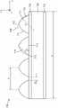
图1为光重定向膜700的示意性剖视图,该光重定向膜包括在基板720上沿第一方向(z方向是指图1所示的x-y-z坐标系)延伸并且沿正交的第二方向(y方向)并排布置的多个基本上平行的间隔开的结构710。结构710可具有小于1mm的至少一个尺寸(例如,结构710的宽度可在约1微米至约500微米的范围内),因此结构710可称为微结构,并且光重定向膜700可称为微结构化膜。FIG. 1 is a schematic cross-sectional view of a
在一些实施方案中,背光源(例如,HDR背光源)包括光重定向膜700中的一个光重定向膜或多个光重定向膜。在一些实施方案中,显示系统包括背光源,该背光源包括多个光重定向膜700中的一个光重定向膜,或以其他方式包括光重定向膜700中的一个光重定向膜或多个光重定向膜。在HDR背光源中通常期望隔离由每个离散光源限定的照明区,以便使串扰最小化。这可通过光重定向膜的截光角来实现,其中输出辉亮度突然降低,从而在每个离散照明区之间形成暗区。截光角由结构形状、其折射率、基板折射率和光重定向膜中的任何漫射层决定。光重定向膜700的可用的几何形状和折射率在本文别处有所描述。In some implementations, a backlight (eg, an HDR backlight) includes a light redirecting film or a plurality of light redirecting films in
每个结构710包括在峰712处交会的相对弯曲小面711。峰712沿第一方向延伸,使得在光重定向膜的位于基本上垂直于第一方向的平面(如图1所示的x-y平面)内的横截面中:结构的相邻峰之间的平均侧向间距为P;结构710的相邻基部713之间的平均侧向间距为W,并且结构的弯曲小面的最佳拟合曲率半径的平均值为R。小面的横截面中的最佳拟合曲率半径为圆的半径,该半径使沿小面的表面的从圆到表面的法线的平方距离最小化。最佳拟合圆的弧709在图1中示出。最佳拟合曲率半径可使用常规最小平方拟合技术来确定。在一些实施方案中,0.1>0.2。在一些实施方案中,0.6>1.1。在一些实施方案中,15微米≤R≤25微米。在一些实施方案中,在光重定向膜的位于基本上垂直于第一方向的平面内的横截面中,从每个结构710的峰712到结构710的基部713的端部715所画出的线714与基部713成约30度至约60度范围内的角度θ。在一些实施方案中,结构710具有折射率n1,并且基板720具有折射率n2,其中n1≥1.5,并且n1–n2≥0.02。在一些实施方案中,n1–n2>0.05。在一些实施方案中,1≥n1–n2≥0.02或0.5≥n1–n2≥0.02。除非另外指明,否则折射率是指532nm下确定的折射率。Each
在例示的实施方案中,光重定向膜700包括设置在基板720的相对主表面上的第一层730和第二层732。在其他实施方案中,可省略第一层730和第二层732中的一者或两者。在一些实施方案中,第一层730和第二层732中的一者或两者为光学漫射器,该光学漫射器可为本文别处进一步描述的任何光学漫射器。在一些实施方案中,第二层732为粘合剂层,并且第一层730为光学漫射器或任选地被省略。粘合剂层可为光学漫射器(例如,包括分散于其中的多个粒子的光学透明粘合剂,其中粒子和粘合剂材料具有例如至少0.01或至少0.03的折射率差)。In the illustrated embodiment, light redirecting
光重定向膜700具有总面积A,该总面积A是指光重定向膜700在y-z平面内的面积(例如,膜的长度乘以膜的宽度)。在一些实施方案中,一个或多个光重定向膜700包括在具有视域的显示系统的背光源中,并且光重定向膜700的面积A至少与显示系统的视域一样大。
在一些实施方案中,结构710包括如图1所示的凸形小面711,并且在一些实施方案中,结构710包括凹形小面。在一些实施方案中,显示系统或背光源包括两个(或更多个)光重定向膜700,并且其中这些膜中的一个膜的结构具有凸形小面,并且这些膜中的另一个膜的结构具有凹形小面。在一些实施方案中,光重定向膜包括位于相邻结构710之间的另外结构。例如,基本上小于结构710的凹形或凸形结构可设置在相邻基部713之间。又如,漫射器(例如,漫射表面结构或漫射涂层)可设置在相邻基部713之间。在相邻结构710之间利用另外结构或漫射器可进一步改善包括光重定向膜700中的一个光重定向膜或多个光重定向膜的背光源的均匀度。例如,当背光源中包括两个交叉的光重定向膜700时,照明区中的光源的输出图像由以下区域形成:光穿过两个膜中的结构710的区域、光穿过一个膜中的结构710和另一个膜中的结构710之间的空间的区域以及光穿过两个膜中的结构710之间的空间的区域。通过在相邻结构710之间选择适当的另外结构或漫射器,可调节这些区域的相对强度以在照明区中赋予改善的均匀度。In some embodiments,
图2A为显示系统2000的示意性分解图,该显示系统包括用于对设置在背光源1000上的显示表面100提供均匀照明的背光源1000。显示表面100是像素化的并且包括多个像素110。在一些实施方案中,多个像素110为能够单独寻址的。在例示的实施方案中,显示表面100为显示面板101的显示表面,该显示面板可为液晶显示面板。背光源1000包括多个离散的间隔开的光源200,该多个离散的间隔开的光源被构造为以一对一的对应关系照射显示表面100中的多个非重叠照明区300;以及设置在多个光源200上并且面向该多个光源的第一微结构化膜400。在例示的实施方案中,背光源1000还包括设置在第一微结构化膜400上的第二微结构化膜500。例如,第一微结构化膜400和第二微结构化膜500中的任一者或两者可为对应于光重定向膜700的光重定向膜。FIG. 2A is a schematic exploded view of a
各种部件在图2A的分解图中示意性地示出为分开的。应当理解,各种部件可设置在彼此之上,使得相邻部件彼此接触。膜可被描述为面向多个光源200,例如,如果膜的主表面大致面向多个光源200。例如,第一微结构化膜400设置在多个光源200上并且面向该多个光源。在例示的实施方案中,第一微结构化膜400包括第一结构410和第一基板420,其中第一基板420设置在第一结构410和光源200之间。背光源1000包括设置在第一微结构化膜400上的第二微结构化膜500,其中第一微结构化膜400设置在第二微结构化膜500和多个光源200之间。在例示的实施方案中,第二微结构化膜500包括第二结构510和第二基板520,其中第二基板520设置在第二结构510和第一结构410之间。The various components are schematically shown separated in the exploded view of Figure 2A. It should be understood that various components may be disposed on top of each other such that adjacent components contact each other. A film may be described as facing the plurality of
可利用第一结构410和第二结构510的其他形状和间距。优选地选择第一结构410和第二结构510的形状和间距,以在跨越每个照明区300的发光强度分布中提供期望的程度的均匀度,同时将由每个光源200发射的光210的大部分(例如,至少80%)限制到相应的照明区300。已经发现,提供这些结果的合适的示例性几何形状包括第一微结构化膜400和第二微结构化膜500,其中第一结构410和第二结构510远离光源200并且具有例如针对光重定向膜700描述的几何形状。光源200之间的平均侧向间距为S1。在一些实施方案中,选择S1,使得当光源200通电时,实现跨越多个照明区300的发光强度分布的期望的程度的均匀度。在一些实施方案中,当显示表面100设置在第一微结构化膜400上并且光源200通电时,由每个光源发射200的至少80%的光210照射显示表面100中的相应照明区300,并且跨越多个照明区300的发光强度分布具有平均值I和标准偏差S,其中S/I<1,或S/I<0.8,或S/I<0.7。例如,在一些实施方案中,S/I在0.2至0.8或至0.7的范围内。在一些实施方案中,当显示表面100设置在第一微结构化膜400上并且光源200通电时,跨越每个照明区300的发光强度分布具有平均值Iz和标准偏差Sz,其中Sz/Iz<0.8,或Sz/Iz<0.6,或Sz/Iz<0.5,或Sz/Iz<0.4。例如,在一些实施方案中,Sz/Iz各自在0.2至0.5或至0.4的范围内。Other shapes and spacings of the
可选择第一微结构化膜400和第二微结构化膜500(例如,选择具有期望的折射率的结构和基板的材料、选择结构的各种几何参数、或基板的厚度)以赋予理想的低S/I和/或Sz/Iz。第一基板420具有厚度H1,并且第二基板520具有厚度H2。在一些实施方案中,第二基板的厚度H2与第一基板的厚度H1的比率小于2、或小于1、或小于0.5。在一些实施方案中,0.01<H2/H1<1或0.02<H2/H1<0.5。The first
对背光源1000进行建模,其中第一微结构化膜400和第二微结构化膜500中的每一者如针对光重定向膜700描述。相邻峰之间的间距P取为24微米,角度θ取为45度,小面的曲率半径R取为16.7微米,并且相邻基部之间的间距W取为4微米。结构和基板的折射率n1和n2分别取为1.64和1.61。光源的发射面积取为200微米×200微米,并且照明区的发射面积取为1mm×1mm。第二微结构化膜500的基板厚度H2取为50微米,并且第一微结构化膜400的基板厚度H1为750微米。确定Sz/Iz为0.25。为了比较,在第一微结构化膜400和第二微结构化膜500未就位的情况下确定Sz/Iz,并且实测为3.65。因此,通过包括第一微结构化膜400和第二微结构化膜500来显著减小Sz/Iz。
图3至图6为背光源1000的强度标准偏差除以平均强度(SDA)随分别通过建模确定的R、W/P、n1(对于固定的n2)和H2/H1变化的曲线图。结果表明,SDA对于特定R和W/P具有最小值,降低H2/H1通常会降低SDA,并且对于基板的给定折射率n2(在这种情况下n2=1.61),增加结构n1的折射率会降低SDA。在一些实施方案中,可用于提供低SDA的微结构化膜实现0.1≤W/P≤0.2,0.6≤R/P≤1.1,n1≥1.5并且n1–n2≥0.02。SDA是如上所述对于单个光源和单个照明区确定的,并且因此对应于Sz/Iz。多个光源和照明区可排列成使得相邻照明区彼此靠近。在这种情况下,SDA值将近似S/I。然而,由于相邻照明区之间的间隙具有比照明区更低的发光强度,因此S/I可略大于Sz/Iz。3-6 are graphs of standard deviation of intensity divided by mean intensity (SDA) for
图2B为背光源1000中所包括的多个离散的间隔开的光源200中的光源200a的示意性剖视图。光源200a具有发射面积E1并且发射光210a。多个光源200具有为发射面积E1的总和的总发射面积E。第一微结构化膜400具有为A的总面积,其中微结构化膜400的总面积是指y-z平面内的面积。在一些实施方案中,0.9<A/E<2。在一些实施方案中,第一微结构化膜400在总发射面积E上方延伸并且1<A/E。在一些实施方案中,A/E<1.9或A/E<1.8。2B is a schematic cross-sectional view of a
图2C为显示表面100的示意性俯视图。示出了照明区S2之间的平均侧向间距和照明区S3的平均侧向尺寸。在一些实施方案中,S2/S3≤0.1。例如,S2/S3可在0.005或0.01至0.1或0.08的范围内。在一些实施方案中,S2/S1≤10。例如,S2/S1可在0.1或0.5至10或8的范围内。在图2C中,照明区300被示意性地示出为包括相对较少数量的像素110,但每个照明区300中可包括显著更多的像素110。例如,每个照明区300可包括至少10个像素、或至少50个像素、或至少100个像素、或至少200个像素。在每个照明区300中使用较大数量的像素允许利用较少的光源200,这可能是期望的。已经发现,可选择第一微结构化膜400和第二微结构化膜500,使得当利用相对较大的照明区300时,每个照明区300基本上填充有来自相应光源200的适当均匀的光。然而,利用较大的照明区300降低了由多个照明区300提供的照明强度变化的分辨率,并且这可能不是期望的。因此,在一些实施方案中,每个照明区中的像素数量不超过10000、或不超过5000、或不超过2000、或不超过1000。在一些实施方案中,每个照明区300包括200个和1000个之间的像素110。像素110中的每个像素可包括多个彩色子像素。例如,每个像素110可包括红色子像素、绿色子像素和蓝色子像素。FIG. 2C is a schematic top view of the
在图2A所示的实施方案中,第一微结构化膜400还包括设置在基板420的相反侧上的第一层430和第二层432。可任选地省略第一层430和第二层432中的一者或两者。在一些实施方案中,第一层430和第二层432中的一者或两者为用于漫射由多个光源发射的光的光学漫射器。在一些实施方案中,光学漫射器具有在约1%至约5%的范围内的平均漫反射率。在一些实施方案中,光学漫射器具有大于约80%的平均漫透射率和小于约10%的平均镜面透射率。在一些实施方案中,光学漫射器的平均漫透射率与光学漫射器的平均镜面透射率的比率大于约10。在一些实施方案中,光学漫射器具有至少5%的光学雾度。In the embodiment shown in FIG. 2A , the first
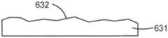
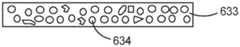
在一些实施方案中,光学漫射器主要为包括微结构化表面的表面漫射器。图7为光学漫射器631的示意性剖视图,该光学漫射器主要为表面漫射器并且具有微结构化表面632。在一些实施方案中,光学漫射器主要为体漫射器。图8为光学漫射器633的示意性剖视图,该光学漫射器主要为体漫射器并且包括分散在其中的粒子634。例如,粒子634可分散在具有与粒子不同的折射率的粘合剂中,如本文别处进一步所述。如果由漫射器散射的垂直入射光的大于50%被漫射器的表面结构散射,则光学漫射器可主要被描述为表面漫射器。在一些实施方案中,由光学漫射器散射的垂直入射光的至少60%、或至少70%、或至少80%、或至少90%由漫射器的表面结构散射。如果由漫射器散射的垂直入射光的大于50%被散射在漫射器的体积中(例如,由分散在漫射器的体积中的粒子散射),则光学漫射器可主要被描述为体漫射器。在一些实施方案中,由光学漫射器散射的垂直入射光的至少60%、或至少70%、或至少80%、或至少90%被散射在漫射器的体积中。In some embodiments, the optical diffuser is primarily a surface diffuser comprising a microstructured surface. FIG. 7 is a schematic cross-sectional view of an
在一些实施方案中,光学漫射器以第一视角A1沿第一方向(例如,在x-y平面内)散射光,并且以第二视角A2沿与第一方向正交的第二方向(例如,在x-z平面内)散射光。例如,光学漫射器可对应于图9A至图9B中示意性地示出的光学漫射器630。光被视为垂直入射在光学漫射器630上并且在示出的视角内透射穿过光学漫射器630,这些视角可为半极大处全宽度(FWHM)视角。在一些实施方案中,A1和A2之间的差值小于5度。在一些实施方案中,A1和A2之间的差值大于5度。可通过使用例如具有不对称表面结构的漫射器或通过在例如通过拉伸至少部分地取向的膜中使用不对称粒子来获得A1和A2之间的差值。In some embodiments, the optical diffuser scatters light along a first direction (e.g., in the x-y plane) at a first viewing angle A1 and along a second direction orthogonal to the first direction (e.g., in the x-y plane) at a second viewing angle A2. in the x-z plane) to scatter light. For example, the optical diffuser may correspond to the
在一些实施方案中,光学漫射器设置在光源200和基板420之间(例如,层432可为光学漫射器)。在一些实施方案中,基板420设置在光源200和光学漫射器之间(例如,层430可为光学漫射器)。In some implementations, an optical diffuser is disposed between
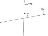
在图2A所示的实施方案中,第二微结构化膜500设置在第一微结构化膜400上。第一微结构化膜400设置在第二微结构化膜500和多个光源200之间,并且包括沿第一方向(沿或大致沿图2A的z方向或沿图2D的第一方向777)延伸并且设置在第一基板420上的多个基本上平行的间隔开的第一结构410。第二微结构化膜500包括沿第二方向(例如,沿或大致沿图2A的y方向或沿图2D的第二方向778)延伸并设置在第二基板520上的多个基本上平行的间隔开的第二结构510。在一些实施方案中,图2D中示意性示出的第一方向777和第二方向778之间的角度φ大于约70度且小于约110度。在一些实施方案中,角度φ大于约80度且小于约100度。在一些实施方案中,角度φ为约90度。第一微结构化膜400设置在第二微结构化膜500和多个光源200之间。第二基板520设置在第二结构510和第一结构410之间。在一些实施方案中,第二微结构化膜500还包括设置在基板520的相反侧上的第一层530和第二层532。第一层530和第二层532可如针对第一层430和第二层432描述。In the embodiment shown in FIG. 2A , second
在一些实施方案中,多个离散的间隔开的光源200中的至少一个光源为发光二极管(例如,图2B所示的光源200a可为发光二极管)。在一些实施方案中,多个离散的间隔开的光源200中的至少一个光源发射蓝光。在一些实施方案中,多个离散的间隔开的光源200中的至少一个光源发射红光。在一些实施方案中,多个离散的间隔开的光源200中的至少一个光源发射绿光。在一些实施方案中,多个离散的间隔开的光源中的至少一个光源发射白光。例如,由图2B所示的光源200A发射的光210a可为蓝光、红光、绿光或白光。在一些实施方案中,光源200中的每个光源为蓝色发光二极管并且包括荧光粉膜以将蓝光的部分转换成红光和绿光,使得透射穿过荧光粉膜的光为白光。在一些实施方案中,荧光粉膜设置在第一微结构化膜400和多个光源200之间。在其他实施方案中,荧光粉膜设置在第二微结构化膜500和显示表面100之间或者第一微结构化膜400和第二微结构化膜500之间。In some embodiments, at least one of the plurality of discrete spaced
在一些实施方案中,多个离散的间隔开的光源200中的每个光源直接放置在第一微结构化膜400的后面并且面向该第一微结构化膜。在一些实施方案中,光源200设置在背反射器600上,用于将由光源200发射的光反射向第一微结构化膜400。在一些实施方案中,多个离散的间隔开的光源200中的至少一个光源(例如,光源200b)大于多个离散的间隔开的光源200中的至少一个其他光源(例如,光源200c)。在其他实施方案中,多个离散的间隔开的光源200中的光源具有基本上相同的大小(例如,所有光源可具有与光源200b相同的大小)。已发现利用背反射器600可改善均匀度(减小SDA)并且增加平均亮度。In some embodiments, each of the plurality of discrete spaced
在一些实施方案中,光源200中的每个光源为能够单独通电的。在一些实施方案中,显示系统2000包括用于对每个像素110单独寻址并且用于对每个光源200单独通电的控制器222。控制器222可适于提供局部调光,其中相对于与所显示图像的较亮区域相关联的光源对与所显示图像的较暗区域相关联的光源进行调光。控制器222中可包括的可用的本地调光控制电路在本领域中是已知的,并且包括在美国专利申请公开2011/0128302(Cho等人)中描述的那些。In some embodiments, each of
多个光源200可被布置成二维阵列,该二维阵列可为周期性阵列(例如,在方格或三角格上)。图10为可设置在显示表面后面的离散的间隔开的光源20的二维阵列的示意性俯视图。可漫反射或镜面反射的反射材料60可设置在光源20之间。例如,光源20可设置在背反射器上,以使得背反射器的处于光源20之间的部分提供反射材料。在一些实施方案中,光源设置在印刷电路板上,并且白色油墨印刷在光源20之间的区域中以提供反射材料60。已经发现,使用反射材料60减小了SDA并增加了结合有离散的间隔开的光源20的二维阵列的显示系统的平均亮度。The plurality of
本说明书的膜可使用任何合适的工艺来制造。在一些实施方案中,通过浇铸和固化工艺或通过任何其他合适的微复制工艺在基板上制备微结构。在包括光学漫射器层的实施方案中,在形成光重定向微结构之前,光学漫射器可作为涂层(例如,含珠漫射器涂层)涂覆到基板的一侧或两侧。另选地,例如,可通过将基板的与其上形成有光重定向微结构的表面相对的表面进行微结构化来制备光学漫射器。光重定向微结构和/或光学漫射微结构可使用具有适当结构化表面的工具制成。该工具可通过金刚石车削工艺形成。结构化表面然后可以连续浇铸和固化工艺形成,其中抵靠工具浇铸树脂并且例如用光化(例如,紫外线(UV))辐射或热来进行固化。连续浇铸和固化工艺的示例描述于以下专利中:美国专利4374077、4576850、5175030、5271968、5558740和5995690。The films of this specification can be fabricated using any suitable process. In some embodiments, the microstructures are fabricated on the substrate by a casting and curing process or by any other suitable microreplication process. In embodiments that include an optical diffuser layer, the optical diffuser can be applied as a coating (e.g., a beaded diffuser coating) to one or both sides of the substrate prior to forming the light redirecting microstructures . Alternatively, for example, an optical diffuser may be prepared by microstructuring the surface of the substrate opposite the surface on which the light redirecting microstructures are formed. Light redirecting microstructures and/or optical diffusing microstructures can be fabricated using tools with appropriately structured surfaces. The tool can be formed by a diamond turning process. The structured surface can then be formed in a continuous casting and curing process in which a resin is cast against a tool and cured, for example, with actinic (eg, ultraviolet (UV)) radiation or heat. Examples of continuous casting and curing processes are described in the following patents: US Pat.
任何合适的材料均可用于基板或微结构。在一些实施方案中,基板为例如聚甲基丙烯酸甲酯(PMMA)膜、聚碳酸酯膜或聚对苯二甲酸乙二醇酯(PET)膜。在一些实施方案中,光重定向微结构例如由诸如丙烯酸酯等能够UV固化的树脂形成。Any suitable material can be used for the substrate or microstructure. In some embodiments, the substrate is, for example, a polymethylmethacrylate (PMMA) film, a polycarbonate film, or a polyethylene terephthalate (PET) film. In some embodiments, the light redirecting microstructures are formed, for example, from a UV curable resin such as acrylate.
以下为本说明书的示例性实施方案的列表。The following is a list of exemplary embodiments of the specification.
实施方案1为一种背光源,该背光源用于对设置在该背光源上的显示表面提供均匀照明,该背光源包括:
多个离散的间隔开的光源,该多个离散的间隔开的光源被构造为以一对一的对应关系照射该显示表面中的多个非重叠照明区;和a plurality of discrete spaced light sources configured to illuminate non-overlapping illumination regions in the display surface in a one-to-one correspondence; and
第一微结构化膜,该第一微结构化膜设置在该多个光源上并且面向该多个光源,使得当该显示表面设置在该第一微结构化膜上并且这些光源通电时,由每个光源发射的至少80%的光照射显示表面中的相应照明区,并且跨越多个照明区的发光强度分布具有平均值I和标准偏差S,S/I<1。A first microstructured film disposed on and facing the plurality of light sources such that when the display surface is disposed on the first microstructured film and the light sources are energized, At least 80% of the light emitted by each light source illuminates a corresponding illuminated area in the display surface, and the luminous intensity distribution across the plurality of illuminated areas has a mean value I and a standard deviation S, S/I<1.
实施方案2为根据实施方案1所述的背光源,其中显示表面为包括多个像素的像素化表面。
实施方案3为根据实施方案2所述的背光源,其中像素为能够单独寻址的。
实施方案4为根据实施方案2所述的背光源,其中每个照明区包括200个和1000个之间的像素。
实施方案5为根据实施方案1所述的背光源,其中该多个离散的间隔开的光源中的每个光源直接放置在该第一微结构化膜的后面并且面向该第一微结构化膜。
实施方案6为根据实施方案1所述的背光源,其中这些光源之间的平均侧向间距为S1,这些照明区之间的平均侧向间距为S2,S2/S1≤10。
实施方案7为根据实施方案1所述的背光源,其中多个光源具有总发射面积E,该第一微结构化膜的总面积为A,0.9<A/E<2。
实施方案8为根据实施方案1所述的背光源,其中相邻照明区之间的平均侧向间距为S2,并且这些照明区的平均侧向尺寸为S3,S2/S3≤0.1。
实施方案9为根据实施方案1所述的背光源,其中第一微结构化膜包括多个基本上平行的间隔开的第一结构,这些第一结构在第一基板上沿第一方向延伸并且沿正交的第二方向并排布置,每个第一结构包括在峰处交会的相对弯曲小面,该峰沿第一方向延伸,第一基板设置在第一结构和光源之间。
实施方案10为根据实施方案9所述的背光源,其中第一微结构化膜还包括用于漫射由多个光源发射的光的光学漫射器。
实施方案11为根据实施方案10所述的背光源,其中光学漫射器具有在约1%至约5%范围内的平均漫反射率。
实施方案12为根据实施方案10所述的背光源,其中光学漫射器具有大于约80%的平均漫透射率和小于约10%的平均镜面透射率。
实施方案13为根据实施方案10所述的背光源,其中光学漫射器的平均漫透射率与光学漫射器的平均镜面透射率的比率大于约10。
实施方案14为根据实施方案9所述的背光源,还包括设置在该第一微结构化膜上的第二微结构化膜,该第一微结构化膜设置在第二微结构化膜和多个光源之间。
实施方案15为根据实施方案14所述的背光源,其中第二微结构化膜包括多个基本上平行的间隔开的第二结构,这些第二结构在第二基板上沿第二方向延伸并且沿第一方向并排布置,每个第二结构包括在峰处交会的相对弯曲小面,该峰沿第二方向延伸,第二基板设置在第二结构和第一结构之间。
实施方案16为根据实施方案1所述的背光源,还包括设置在第一微结构化膜上的第二微结构化膜,第一微结构化膜设置在第二微结构化膜和多个光源之间,并且包括沿第一方向延伸并且设置在第一基板上的多个基本上平行的间隔开的第一结构,第二微结构化膜包括沿第二方向延伸并且设置在第二基板上的多个基本上平行的间隔开的第二结构,第一方向和第二方向之间的角度大于约70度且小于约110度。Embodiment 16 is the backlight of
实施方案17为根据实施方案1所述的背光源,使得当显示表面设置在第一微结构化膜上并且这些光源通电时,跨越每个照明区的发光强度分布具有平均值Iz和标准偏差Sz,Sz/Iz<0.8。Embodiment 17 is the backlight of
实施方案18为一种光重定向膜,包括:Embodiment 18 is a light redirecting film comprising:
多个基本上平行的间隔开的结构,该多个基本上平行的间隔开的结构在基板上沿第一方向延伸并且沿正交的第二方向并排布置,每个结构包括在峰处交会的相对弯曲小面,该峰沿第一方向延伸,使得在光重定向膜的位于基本上垂直于第一方向的平面内的横截面中:a plurality of substantially parallel spaced-apart structures extending in a first direction on the substrate and arranged side-by-side in a second orthogonal direction, each structure comprising a Relative to the curved facet, the peak extends along the first direction such that in a cross-section of the light redirecting film lying in a plane substantially perpendicular to the first direction:
这些结构的相邻峰之间的平均侧向间距为P;The average lateral spacing between adjacent peaks of these structures is P;
这些结构的相邻基部之间的平均侧向间距为W,0.1≤W/P≤0.2;并且The average lateral spacing between adjacent bases of these structures is W, 0.1≤W/P≤0.2; and
这些结构的这些弯曲小面的最佳拟合曲率半径的平均值为R,0.6≤R/P≤1.1。这些结构具有折射率n1,基板具有折射率n2,n1≥1.5,n1–n2≥0.02。The average value of the best-fit radii of curvature for these curved facets of these structures is R, 0.6≤R/P≤1.1. The structures have a refractive index n1 and the substrate has a refractive index n2, n1 ≥ 1.5, n1–n2 ≥ 0.02.
实施方案19为根据实施方案18所述的光重定向膜,其中15微米≤R≤25微米。Embodiment 19 is the light redirecting film of embodiment 18, wherein 15 microns < R < 25 microns.
实施方案20为根据实施方案18所述的光重定向膜,其中在光重定向膜的位于基本上垂直于第一方向的平面内的该横截面中,从每个结构的峰到该结构的基部的端部所画出的线与该基部成约30度至约60度范围内的角度。
实施方案21为一种背光源,该背光源用于对设置在该背光源上的显示表面提供均匀照明,该背光源包括:Embodiment 21 is a backlight for providing uniform illumination to a display surface disposed on the backlight, the backlight comprising:
多个离散的间隔开的光源,该多个离散的间隔开的光源被构造为以一对一的对应关系照射显示表面中的多个非重叠照明区;和a plurality of discrete spaced light sources configured to illuminate a plurality of non-overlapping illumination regions in the display surface in a one-to-one correspondence; and
根据实施方案18至20中任一项所述的光重定向膜,该光重定向膜设置在该多个光源上并且面向该多个光源,使得当显示表面设置在光重定向膜上并且这些光源通电时,由每个光源发射的至少80%的光照射显示表面中的相应照明区,并且跨越多个照明区的发光强度分布具有平均值I和标准偏差S,S/I<1。The light redirecting film according to any one of embodiments 18 to 20, the light redirecting film is disposed on and faces the plurality of light sources such that when a display surface is disposed on the light redirecting film and the When the light sources are energized, at least 80% of the light emitted by each light source illuminates a corresponding illumination zone in the display surface, and the luminous intensity distribution across the plurality of illumination zones has a mean I and a standard deviation S, S/I<1.
实施方案22为一种显示系统,包括:Embodiment 22 is a display system, comprising:
像素化显示表面,该像素化显示表面包括多个像素和多个非重叠照明区,每个照明区包括这些像素中的至少10个像素;a pixelated display surface comprising a plurality of pixels and a plurality of non-overlapping illumination regions, each illumination region comprising at least 10 of the pixels;
离散的间隔开的光源的二维阵列,该离散的间隔开的光源的二维阵列设置在显示表面的后面,每个光源与这些照明区中的一个照明区成一对一的对应关系;和a two-dimensional array of discrete spaced light sources disposed behind the display surface, each light source in a one-to-one correspondence with one of the illumination zones; and
控制器,该控制器用于对每个像素单独寻址并且用于对每个光源单独通电,使得当通电时,由每个光源发射的至少80%的光照射对应于光源的照明区。A controller for individually addressing each pixel and for individually energizing each light source such that when energized, at least 80% of the light emitted by each light source illuminates the illumination area corresponding to the light source.
实施方案23为根据实施方案22所述的显示系统,还包括背光源,该背光源包括离散的间隔开的光源的二维阵列。Embodiment 23 is the display system of embodiment 22, further comprising a backlight comprising a two-dimensional array of discrete spaced light sources.
实施方案24为根据实施方案23所述的显示系统,其中背光源还包括设置在像素化显示表面和离散的间隔开的光源的二维阵列之间的微结构化膜。Embodiment 24 is the display system of embodiment 23, wherein the backlight further comprises a microstructured film disposed between the pixelated display surface and the two-dimensional array of discrete spaced light sources.
实施方案25为根据实施方案24所述的显示系统,其中微结构化膜为根据实施方案18至20中任一项所述的光重定向膜。Embodiment 25 is the display system of embodiment 24, wherein the microstructured film is the light redirecting film of any one of embodiments 18-20.
实施方案26为根据实施方案23所述的显示系统,其中背光源还根据实施方案1至17中任一项来表征。Embodiment 26 is the display system of embodiment 23, wherein the backlight is further characterized according to any one of embodiments 1-17.
实施方案27为根据实施方案1至17中任一项所述的背光源,其中第一微结构化膜为根据实施方案18至20中任一项所述的光重定向膜。Embodiment 27 is the backlight of any one of embodiments 1-17, wherein the first microstructured film is the light redirecting film of any one of embodiments 18-20.
如果本领域普通技术人员在本说明书中使用和描述的上下文中对“约”应用于表达特征大小、数量和物理特性的量的使用不清楚,则“约”将被理解为是指在指定值的10%以内。给定为约指定值的量可精确地为指定值。例如,如果本领域普通技术人员在本说明书中使用和描述的上下文中对其不清楚,则具有约1的值的量是指该量具有介于0.9和1.1之间的值,并且该值可为1。If the use of "about" applied to a quantity expressing a characteristic size, quantity, and physical property is unclear to a person of ordinary skill in the art in the context of use and description in this specification, then "about" will be understood to mean within 10% of. An amount given as about a specified value may be exactly the specified value. For example, an amount having a value of about 1 means that the amount has a value between 0.9 and 1.1, and the value can be is 1.
上述所有引用的参考文献、专利和专利申请以一致的方式全文据此以引用方式并入本文。在并入的参考文献部分与本申请之间存在不一致或矛盾的情况下,应以前述说明中的信息为准。All references, patents, and patent applications cited above are hereby incorporated by reference in their entirety in their entirety. In the event of an inconsistency or contradiction between an incorporated reference section and the present application, the information in the foregoing description shall control.
除非另外指明,否则针对附图中元件的描述应被理解为同样应用于其他附图中的相应元件。虽然本文已经例示并描述了具体实施方案,但本领域的普通技术人员将会知道,在不脱离本公开范围的情况下,可用多种另选的和/或等同形式的具体实施来代替所示出和所描述的具体实施方案。本申请旨在涵盖本文所讨论的具体实施方案的任何改型或变型。因此,本公开旨在仅受权利要求及其等同形式的限制。Unless otherwise specified, descriptions for elements in one drawing should be understood to apply to corresponding elements in other figures as well. While specific embodiments have been illustrated and described herein, those of ordinary skill in the art will recognize that various alternative and/or equivalent implementations may be used in place of the embodiments shown without departing from the scope of the present disclosure. Specific embodiments shown and described. This application is intended to cover any adaptations or variations of the specific embodiments discussed herein. Accordingly, it is intended that this disclosure be limited only by the claims and the equivalents thereof.
Claims (13)
Applications Claiming Priority (3)
| Application Number | Priority Date | Filing Date | Title |
|---|---|---|---|
| US201862666487P | 2018-05-03 | 2018-05-03 | |
| US62/666,487 | 2018-05-03 | ||
| PCT/IB2019/053540WO2019211752A1 (en) | 2018-05-03 | 2019-04-30 | Light redirecting film, backlight, and display system |
Publications (2)
| Publication Number | Publication Date |
|---|---|
| CN112105866A CN112105866A (en) | 2020-12-18 |
| CN112105866Btrue CN112105866B (en) | 2023-02-17 |
Family
ID=68387030
Family Applications (1)
| Application Number | Title | Priority Date | Filing Date |
|---|---|---|---|
| CN201980029560.0AActiveCN112105866B (en) | 2018-05-03 | 2019-04-30 | Light redirecting film, backlight and display system |
Country Status (6)
| Country | Link |
|---|---|
| US (1) | US11175533B2 (en) |
| JP (1) | JP7369717B2 (en) |
| KR (1) | KR20200140307A (en) |
| CN (1) | CN112105866B (en) |
| TW (1) | TW201947289A (en) |
| WO (1) | WO2019211752A1 (en) |
Families Citing this family (3)
| Publication number | Priority date | Publication date | Assignee | Title |
|---|---|---|---|---|
| CN112083599A (en)* | 2019-06-14 | 2020-12-15 | 群创光电股份有限公司 | display screen |
| CN113589420A (en)* | 2021-07-23 | 2021-11-02 | 北京字节跳动网络技术有限公司 | Light guide plate and lamp |
| CN117872643A (en)* | 2024-02-01 | 2024-04-12 | 武汉华星光电技术有限公司 | Backlight module and liquid crystal display module |
Citations (10)
| Publication number | Priority date | Publication date | Assignee | Title |
|---|---|---|---|---|
| CN101535878A (en)* | 2006-11-15 | 2009-09-16 | 3M创新有限公司 | Back-lit displays with high illumination uniformity |
| CN101535880A (en)* | 2006-11-15 | 2009-09-16 | 3M创新有限公司 | Back-lit displays with high illumination uniformity |
| CN101946206A (en)* | 2008-02-15 | 2011-01-12 | 3M创新有限公司 | Be used to improve the brightness enhancement film of display uniformity of illuminance and the diffusion sheet of based thin film |
| CN102483544A (en)* | 2009-09-11 | 2012-05-30 | 杜比实验室特许公司 | Displays incorporating leaky reflectors |
| CN102483473A (en)* | 2009-08-25 | 2012-05-30 | 3M创新有限公司 | Light redirecting film and display system incorporating same |
| CN104344291A (en)* | 2014-09-11 | 2015-02-11 | 友达光电股份有限公司 | Backlight module |
| CN104930399A (en)* | 2014-03-17 | 2015-09-23 | Nlt科技股份有限公司 | Surface light-emitting device and liquid crystal display apparatus |
| CN106816502A (en)* | 2017-04-12 | 2017-06-09 | 京东方科技集团股份有限公司 | A kind of LED chip, LED light-emitting substrates, display device and color display control method |
| WO2017204840A1 (en)* | 2016-05-23 | 2017-11-30 | Leia Inc. | Diffractive multibeam element-based backlighting |
| CN107533188A (en)* | 2015-04-24 | 2018-01-02 | 3M创新有限公司 | Optical film |
Family Cites Families (31)
| Publication number | Priority date | Publication date | Assignee | Title |
|---|---|---|---|---|
| US4576850A (en) | 1978-07-20 | 1986-03-18 | Minnesota Mining And Manufacturing Company | Shaped plastic articles having replicated microstructure surfaces |
| US4374077A (en) | 1980-02-01 | 1983-02-15 | Minnesota Mining And Manufacturing Company | Process for making information carrying discs |
| US5175030A (en) | 1989-02-10 | 1992-12-29 | Minnesota Mining And Manufacturing Company | Microstructure-bearing composite plastic articles and method of making |
| US5271968A (en) | 1990-02-20 | 1993-12-21 | General Electric Company | Method for production of an acrylic coated polycarbonate article |
| US5558740A (en) | 1995-05-19 | 1996-09-24 | Reflexite Corporation | Method and apparatus for producing seamless retroreflective sheeting |
| US5995690A (en) | 1996-11-21 | 1999-11-30 | Minnesota Mining And Manufacturing Company | Front light extraction film for light guiding systems and method of manufacture |
| EP1390806B1 (en) | 2001-02-27 | 2010-08-25 | Dolby Laboratories Licensing Corporation | High dynamic range display devices |
| AU2002359708A1 (en)* | 2001-12-14 | 2003-07-15 | Digital Optics International Corporation | Uniform illumination system |
| US7052152B2 (en) | 2003-10-03 | 2006-05-30 | Philips Lumileds Lighting Company, Llc | LCD backlight using two-dimensional array LEDs |
| US7997771B2 (en) | 2004-06-01 | 2011-08-16 | 3M Innovative Properties Company | LED array systems |
| KR101298786B1 (en) | 2005-08-27 | 2013-08-22 | 쓰리엠 이노베이티브 프로퍼티즈 컴파니 | Illumination assembly and system |
| US20090284954A1 (en)* | 2005-10-28 | 2009-11-19 | Yukinori Yamada | Backlight device, display device, and optical member |
| US7843637B2 (en)* | 2006-06-22 | 2010-11-30 | 3M Innovative Properties Company | Birefringent structured film for LED color mixing in a backlight |
| US20080049330A1 (en)* | 2006-08-25 | 2008-02-28 | 3M Innovative Properties Company | Light directing laminate |
| WO2008053790A1 (en)* | 2006-10-27 | 2008-05-08 | Fujifilm Corporation | Backlight unit |
| US7766528B2 (en) | 2006-11-15 | 2010-08-03 | 3M Innovative Properties Company | Back-lit displays with high illumination uniformity |
| US20080111947A1 (en)* | 2006-11-15 | 2008-05-15 | 3M Innovative Properties Company | Back-lit displays with high illumination uniformity |
| US7478913B2 (en) | 2006-11-15 | 2009-01-20 | 3M Innovative Properties | Back-lit displays with high illumination uniformity |
| US20080231780A1 (en)* | 2007-03-22 | 2008-09-25 | Sabic Innovative Plastics Ip Bv | Low-absorptive diffuser sheet and film stacks for direct-lit backlighting |
| JP2008311026A (en)* | 2007-06-13 | 2008-12-25 | Mitsubishi Rayon Co Ltd | Surface light source device |
| JP5245659B2 (en)* | 2008-09-08 | 2013-07-24 | 凸版印刷株式会社 | Optical device, uniform light device, backlight unit and display device |
| US20100128351A1 (en) | 2008-11-21 | 2010-05-27 | 3M Innovative Properties Company | Curved sided cone structures for controlling gain and viewing angle in an optical film |
| KR101617485B1 (en)* | 2008-12-05 | 2016-05-02 | 도판 인사츠 가부시키가이샤 | Optical component, lighting device, and display device |
| KR101295882B1 (en) | 2009-11-30 | 2013-08-12 | 엘지디스플레이 주식회사 | Liquid crystal display and local dimming control method of thereof |
| TWI561770B (en)* | 2010-04-30 | 2016-12-11 | Samsung Electronics Co Ltd | Light emitting device package, light source module, backlight unit, display apparatus, television set, and illumination apparatus |
| EP2577151B1 (en)* | 2010-05-28 | 2016-09-21 | Philips Lighting Holding B.V. | A beamshaping optical stack, a light source and a luminaire |
| US8789959B2 (en)* | 2010-08-31 | 2014-07-29 | Sharp Kabushiki Kaisha | Lighting device, display device and television device |
| JP2013109242A (en)* | 2011-11-22 | 2013-06-06 | Yukio Yamamoto | Liquid crystal display device |
| JP6202828B2 (en)* | 2012-02-17 | 2017-09-27 | 学校法人慶應義塾 | Liquid crystal display |
| KR101878800B1 (en) | 2012-04-04 | 2018-07-17 | 엘지디스플레이 주식회사 | Liquid crystal display device |
| GB201705365D0 (en)* | 2017-04-03 | 2017-05-17 | Optovate Ltd | Illumination apparatus |
- 2019
- 2019-04-30CNCN201980029560.0Apatent/CN112105866B/enactiveActive
- 2019-04-30WOPCT/IB2019/053540patent/WO2019211752A1/ennot_activeCeased
- 2019-04-30KRKR1020207031231Apatent/KR20200140307A/ennot_activeCeased
- 2019-04-30USUS17/041,028patent/US11175533B2/enactiveActive
- 2019-04-30JPJP2020561797Apatent/JP7369717B2/enactiveActive
- 2019-05-02TWTW108115244Apatent/TW201947289A/enunknown
Patent Citations (10)
| Publication number | Priority date | Publication date | Assignee | Title |
|---|---|---|---|---|
| CN101535878A (en)* | 2006-11-15 | 2009-09-16 | 3M创新有限公司 | Back-lit displays with high illumination uniformity |
| CN101535880A (en)* | 2006-11-15 | 2009-09-16 | 3M创新有限公司 | Back-lit displays with high illumination uniformity |
| CN101946206A (en)* | 2008-02-15 | 2011-01-12 | 3M创新有限公司 | Be used to improve the brightness enhancement film of display uniformity of illuminance and the diffusion sheet of based thin film |
| CN102483473A (en)* | 2009-08-25 | 2012-05-30 | 3M创新有限公司 | Light redirecting film and display system incorporating same |
| CN102483544A (en)* | 2009-09-11 | 2012-05-30 | 杜比实验室特许公司 | Displays incorporating leaky reflectors |
| CN104930399A (en)* | 2014-03-17 | 2015-09-23 | Nlt科技股份有限公司 | Surface light-emitting device and liquid crystal display apparatus |
| CN104344291A (en)* | 2014-09-11 | 2015-02-11 | 友达光电股份有限公司 | Backlight module |
| CN107533188A (en)* | 2015-04-24 | 2018-01-02 | 3M创新有限公司 | Optical film |
| WO2017204840A1 (en)* | 2016-05-23 | 2017-11-30 | Leia Inc. | Diffractive multibeam element-based backlighting |
| CN106816502A (en)* | 2017-04-12 | 2017-06-09 | 京东方科技集团股份有限公司 | A kind of LED chip, LED light-emitting substrates, display device and color display control method |
Also Published As
| Publication number | Publication date |
|---|---|
| TW201947289A (en) | 2019-12-16 |
| US20210141272A1 (en) | 2021-05-13 |
| KR20200140307A (en) | 2020-12-15 |
| CN112105866A (en) | 2020-12-18 |
| JP7369717B2 (en) | 2023-10-26 |
| JP2021522664A (en) | 2021-08-30 |
| WO2019211752A1 (en) | 2019-11-07 |
| US11175533B2 (en) | 2021-11-16 |
Similar Documents
| Publication | Publication Date | Title |
|---|---|---|
| US10247872B2 (en) | Dual-sided film with split light spreading structures | |
| TWI831941B (en) | Mode-switchable backlight, privacy display, and method employing emitter arrays | |
| US7165874B2 (en) | Backlight unit and liquid crystal display device | |
| TWI762910B (en) | Time-multiplexed backlight, multiview display, and method | |
| US11204458B2 (en) | Wide-area solid-state illumination devices and systems employing sheet-form light guides and method of making the same | |
| JP7583040B2 (en) | Privacy mode backlight, privacy display and method | |
| CN106170720B (en) | Asymmetric turning film with multiple light sources | |
| CN110462285A (en) | Mode switchable backlight, privacy display and method | |
| KR101443564B1 (en) | Illumination system and display device | |
| EP1813859A1 (en) | Light guide plate, surface illuminator using same and liquid crystal display | |
| JP2009070826A (en) | Surface lighting device | |
| CN112105866B (en) | Light redirecting film, backlight and display system | |
| JP2022530369A (en) | Multi-zone backlight, multi-view display, and method | |
| JP5228785B2 (en) | Microlens sheet and backlight unit / display device using the same | |
| JP2009300989A (en) | Light deflection sheet and surface light source apparatus equipped with the same | |
| JP2010218693A (en) | Light guide plate for point-like light source | |
| CN104704290A (en) | Thin and efficient light guide system | |
| JP2004325505A (en) | Back-lighting device and liquid crystal display device | |
| CN223022498U (en) | Backlight unit | |
| JP2012190582A (en) | Lighting unit, lighting device, and display device | |
| JP2007073226A (en) | Transmittance adjuster unit, planar illumination device using the same, and liquid crystal display device | |
| JP2006318754A (en) | Transmissivity adjuster unit, planar illumination device, and liquid crystal display device using planer illumination device | |
| KR20120056468A (en) | Light emitting module, backlight unit and display device including the same | |
| JP2006339043A (en) | Planar lighting device, and liquid crystal display device with same |
Legal Events
| Date | Code | Title | Description |
|---|---|---|---|
| PB01 | Publication | ||
| PB01 | Publication | ||
| SE01 | Entry into force of request for substantive examination | ||
| SE01 | Entry into force of request for substantive examination | ||
| GR01 | Patent grant | ||
| GR01 | Patent grant |