CN112099141A - Diffraction optical waveguide, manufacturing method, method and equipment for improving uniformity of emergent light - Google Patents
Diffraction optical waveguide, manufacturing method, method and equipment for improving uniformity of emergent lightDownload PDFInfo
- Publication number
- CN112099141A CN112099141ACN202011185675.XACN202011185675ACN112099141ACN 112099141 ACN112099141 ACN 112099141ACN 202011185675 ACN202011185675 ACN 202011185675ACN 112099141 ACN112099141 ACN 112099141A
- Authority
- CN
- China
- Prior art keywords
- refractive index
- change material
- coupling
- material film
- phase
- Prior art date
- Legal status (The legal status is an assumption and is not a legal conclusion. Google has not performed a legal analysis and makes no representation as to the accuracy of the status listed.)
- Granted
Links
- 230000003287optical effectEffects0.000titleclaimsabstractdescription49
- 238000000034methodMethods0.000titleclaimsabstractdescription34
- 238000004519manufacturing processMethods0.000titleclaimsabstractdescription20
- 239000012782phase change materialSubstances0.000claimsdescription75
- 230000008859changeEffects0.000claimsdescription43
- 238000010438heat treatmentMethods0.000claimsdescription15
- 230000005284excitationEffects0.000claimsdescription8
- 238000007747platingMethods0.000claims2
- 238000010168coupling processMethods0.000description31
- 238000005859coupling reactionMethods0.000description31
- 230000010344pupil dilationEffects0.000description19
- 239000011248coating agentSubstances0.000description8
- 238000000576coating methodMethods0.000description8
- 238000010586diagramMethods0.000description8
- 239000000463materialSubstances0.000description3
- 230000008569processEffects0.000description3
- 230000006872improvementEffects0.000description2
- 230000007704transitionEffects0.000description2
- 238000000137annealingMethods0.000description1
- 230000008878couplingEffects0.000description1
- 239000013078crystalSubstances0.000description1
- 230000000694effectsEffects0.000description1
- 238000004049embossingMethods0.000description1
- 238000002474experimental methodMethods0.000description1
- 238000012634optical imagingMethods0.000description1
- 238000000206photolithographyMethods0.000description1
- 210000001747pupilAnatomy0.000description1
- 238000004088simulationMethods0.000description1
- 239000000758substrateSubstances0.000description1
Images


Classifications
- G—PHYSICS
- G02—OPTICS
- G02B—OPTICAL ELEMENTS, SYSTEMS OR APPARATUS
- G02B6/00—Light guides; Structural details of arrangements comprising light guides and other optical elements, e.g. couplings
- G02B6/10—Light guides; Structural details of arrangements comprising light guides and other optical elements, e.g. couplings of the optical waveguide type
- G02B6/12—Light guides; Structural details of arrangements comprising light guides and other optical elements, e.g. couplings of the optical waveguide type of the integrated circuit kind
- G02B6/122—Basic optical elements, e.g. light-guiding paths
- G02B6/124—Geodesic lenses or integrated gratings
- G—PHYSICS
- G02—OPTICS
- G02B—OPTICAL ELEMENTS, SYSTEMS OR APPARATUS
- G02B27/00—Optical systems or apparatus not provided for by any of the groups G02B1/00 - G02B26/00, G02B30/00
- G02B27/01—Head-up displays
- G02B27/017—Head mounted
- G02B27/0172—Head mounted characterised by optical features
- G—PHYSICS
- G02—OPTICS
- G02B—OPTICAL ELEMENTS, SYSTEMS OR APPARATUS
- G02B5/00—Optical elements other than lenses
- G02B5/18—Diffraction gratings
- G02B5/1847—Manufacturing methods
Landscapes
- Physics & Mathematics (AREA)
- General Physics & Mathematics (AREA)
- Optics & Photonics (AREA)
- Engineering & Computer Science (AREA)
- Microelectronics & Electronic Packaging (AREA)
- Manufacturing & Machinery (AREA)
- Diffracting Gratings Or Hologram Optical Elements (AREA)
Abstract
Description
Translated fromChinese技术领域technical field
本发明涉及光学成像技术领域,更为具体地,涉及一种提高出射光均匀性的衍射光波导及其制造方法、提高衍射光波导出射光均匀性的方法、头戴显示设备。The invention relates to the technical field of optical imaging, and more particularly, to a diffractive optical waveguide for improving the uniformity of emitted light, a method for manufacturing the same, a method for improving the uniformity of emitted light from the diffracted optical waveguide, and a head-mounted display device.
背景技术Background technique
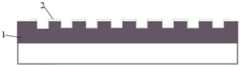
现有的衍射光波导结构光路,较多运用到的是表面浮雕光栅(Surfacereliefgrating,SRG)。表面浮雕光栅通常在基底上划刻光栅结构或者采用光刻的方式压印光栅结构,分为一维光栅和二维光栅。但是二者都是均匀光栅,光栅常数和光栅深度都是相同的,由于其自身的特性,在耦出区域的光线能量会沿着光线在光波导内部的传播方向(扩瞳方向)越来越低,导致出射的光线亮度不均匀,人眼就会看到一个明暗不同的图案,如图1所示,衍射光波导10耦出区域图像沿扩瞳方向亮度变化明显,图中上方圆点表示图像,明暗代表出射光线亮度大小。In the existing diffractive optical waveguide structure optical path, surface relief grating (SRG) is mostly used. Surface relief gratings are usually divided into one-dimensional gratings and two-dimensional gratings by scribing the grating structure on the substrate or imprinting the grating structure by photolithography. However, both are uniform gratings with the same grating constant and grating depth. Due to their own characteristics, the light energy in the outcoupling region will become more and more along the propagation direction (pupil dilation direction) of the light inside the optical waveguide. If the value is low, the brightness of the outgoing light is uneven, and the human eye will see a pattern with different brightness and darkness. As shown in Figure 1, the brightness of the image of the outcoupling area of the diffractive
目前,改善这种亮度不均匀性的方法主要有两种:一是改变光栅深度,使不同耦出区域的深度不同。但是这种光栅难以设计,并且很难加工,没有量产的可行性;二是改变光栅周期,但是这种方法的改善效果有限。At present, there are two main methods to improve this brightness non-uniformity: one is to change the grating depth, so that the depths of different out-coupling regions are different. However, this kind of grating is difficult to design and process, and there is no feasibility of mass production; the second is to change the grating period, but the improvement effect of this method is limited.
发明内容SUMMARY OF THE INVENTION
鉴于上述问题,本发明的目的是提供一种出射亮度均匀的衍射光波导及其制造方法、头戴显示设备及提高衍射光波导出射光线均匀性的方法。In view of the above problems, the object of the present invention is to provide a diffractive optical waveguide with uniform emission brightness, a manufacturing method thereof, a head-mounted display device, and a method for improving the uniformity of light emitted from the diffracted optical waveguide.
根据本发明的一个方面,提供一种提高出射光均匀性的衍射光波导,包括衍射光栅和涂敷在衍射光栅上的折射率渐变膜,通过不同耦出区域的折射率渐变膜的折射率变化提高耦出光线亮度的均匀性。According to one aspect of the present invention, a diffractive optical waveguide for improving the uniformity of the outgoing light is provided, comprising a diffraction grating and a graded refractive index film coated on the diffraction grating, and the refractive index changes of the graded refractive index film through different outcoupling regions Improve the uniformity of the brightness of the out-coupled light.
优选地,所述折射率渐变膜为相变材料。Preferably, the graded refractive index film is a phase change material.
进一步,优选地,所述相变材料包括Ge2Sb2Te5。Further, preferably, the phase change material includes Ge2Sb2Te5.
根据本发明的另一个方面,提供一种头戴显示设备,上述衍射光波导。According to another aspect of the present invention, there is provided a head-mounted display device, the above-mentioned diffractive optical waveguide.
根据本发明的第三个方面,提供一种提高出射光均匀性的衍射光波导的制造方法,包括:According to a third aspect of the present invention, there is provided a method for manufacturing a diffractive optical waveguide that improves the uniformity of emitted light, comprising:
在衍射光栅上镀相变材料薄膜;Coating the phase change material film on the diffraction grating;
使得相变材料薄膜按照耦出区域亮度变化而变化,获得涂覆在衍射光栅上的折射率渐变膜。The phase-change material film is changed according to the brightness change of the out-coupling area, and a refractive index gradient film coated on the diffraction grating is obtained.
优选地,所述使得相变材料薄膜按照耦出区域亮度变化而变化的步骤包括:Preferably, the step of making the phase change material film change according to the brightness change of the out-coupling area includes:
通过加热方式使得相变材料薄膜随温度按照耦出区域亮度变化阶梯变化。By heating, the phase change material film changes stepwise with temperature according to the brightness change of the coupling-out area.
优选地,所述使得相变材料薄膜按照耦出区域亮度变化而变化的步骤包括:Preferably, the step of making the phase change material film change according to the brightness change of the out-coupling area includes:
通过激光照射方式使得相变材料薄膜的折射率随温度按照耦出区域亮度变化阶梯变化。By means of laser irradiation, the refractive index of the phase change material film changes stepwise with temperature according to the brightness change of the coupling-out region.
优选地,所述使得相变材料薄膜按照耦出区域亮度变化而变化的步骤包括:Preferably, the step of making the phase change material film change according to the brightness change of the out-coupling area includes:
通过电激励的方式使得相变材料薄膜的折射率随温度按照耦出区域亮度变化阶梯变化。By means of electrical excitation, the refractive index of the phase-change material film changes stepwise with temperature according to the brightness change of the out-coupling area.
根据本发明的第四个方面,提供一种提高衍射光波导的出射光均匀性的方法,包括:According to a fourth aspect of the present invention, there is provided a method for improving the uniformity of light emitted from a diffractive optical waveguide, comprising:
在衍射光波导耦出区域的衍射光栅上镀相变材料薄膜;Coating a phase change material film on the diffraction grating in the out-coupling area of the diffractive optical waveguide;
使得相变材料薄膜的折射率按照耦出区域亮度变化而变化,获得涂覆在衍射光栅上的折射率渐变膜。The refractive index of the phase-change material film is changed according to the change of the brightness of the out-coupling region to obtain a graded refractive index film coated on the diffraction grating.
优选地,所述使得相变材料薄膜的折射率按照耦出区域亮度变化而变化的步骤包括:Preferably, the step of changing the refractive index of the phase change material film according to the change of the brightness of the out-coupling area includes:
通过加热方式、激光照射方式或/和电激励的方式使得相变材料薄膜的折射率随温度按照耦出区域亮度变化阶梯变化。The refractive index of the phase change material film changes stepwise with temperature according to the brightness change of the coupling-out region by heating, laser irradiation or/and electrical excitation.
上述提高出射光均匀性的衍射光波导及其制造方法、提高衍射光波导出射光均匀性的方法、头戴显示设备通过使得涂覆在衍射光栅结构上的折射率渐变膜的折射率按照耦出区域亮度变化渐变,从而在不改变光栅设计参数的前提下,使衍射光波导耦出光线亮度均匀,并且具有价格低廉、工艺难度低、适合量产的特点。The above-mentioned diffractive optical waveguide for improving the uniformity of the outgoing light and the manufacturing method thereof, the method for improving the uniformity of the outgoing light from the diffracted optical waveguide, and the head-mounted display device The brightness changes gradually, so that the brightness of the light coupled out of the diffractive optical waveguide is uniform without changing the design parameters of the grating, and it has the characteristics of low price, low process difficulty and suitable for mass production.
为了实现上述以及相关目的,本发明的一个或多个方面包括后面将详细说明特别指出的特征。下面的说明以及附图详细说明了本发明的某些示例性方面。然而,这些方面指示的仅仅是可使用本发明的原理的各种方式中的一些方式。此外,本发明旨在包括所有这些方面以及它们的等同物。To carry out the above and related objects, one or more aspects of the invention comprise the features particularly pointed out in the following detailed description. The following description and accompanying drawings illustrate certain exemplary aspects of the invention in detail. These aspects are indicative, however, of but a few of the various ways in which the principles of the invention may be employed. Furthermore, the present invention is intended to include all such aspects and their equivalents.
附图说明Description of drawings
通过参考以下结合附图的说明内容,并且随着对本发明的更全面理解,本发明的其它目的及结果将更加明白及易于理解。在附图中:Other objects and results of the present invention will be more apparent and readily understood by reference to the following description in conjunction with the accompanying drawings, and as the present invention is more fully understood. In the attached image:
图1是衍射光波导不同耦出区域的图像亮度示意图;Fig. 1 is a schematic diagram of the image brightness of different outcoupling regions of the diffractive optical waveguide;
图2是本发明所述提高出射光均匀性的衍射光波导的示意图;2 is a schematic diagram of the diffractive optical waveguide for improving the uniformity of the emitted light according to the present invention;
图3是本发明所述提高出射光均匀性的衍射光波导的制造方法的流程示意图;3 is a schematic flow chart of the method for manufacturing a diffractive optical waveguide for improving the uniformity of emitted light according to the present invention;
图4是本发明所述提高出射光均匀性的衍射光波导的制造方法的一个实施例的示意图;4 is a schematic diagram of an embodiment of the method for manufacturing a diffractive optical waveguide for improving the uniformity of the emitted light according to the present invention;
图5是本发明所述提高出射光均匀性的衍射光波导的制造方法的另一个实施例的示意图;FIG. 5 is a schematic diagram of another embodiment of the method for manufacturing a diffractive optical waveguide for improving the uniformity of emitted light according to the present invention;
图6是本发明所述提高出射光均匀性的衍射光波导的制造方法的第三个实施例的示意图;6 is a schematic diagram of a third embodiment of the method for manufacturing a diffractive optical waveguide for improving the uniformity of the emitted light according to the present invention;
图7是使得衍射光波导出射光线亮度均匀的沿扩瞳方向的折射率变化图;Fig. 7 is the refractive index change diagram along the pupil dilation direction that makes the brightness of the light emitted by the diffracted light waveguide uniform;
图8是本发明所述衍射光波导的不同耦出区域的图像的亮度示意图。FIG. 8 is a schematic diagram of brightness of images of different outcoupling regions of the diffractive optical waveguide according to the present invention.
在所有附图中相同的标号指示相似或相应的特征或功能。The same reference numbers indicate similar or corresponding features or functions throughout the drawings.
具体实施方式Detailed ways
以下将结合附图对本发明的具体实施例进行详细描述。The specific embodiments of the present invention will be described in detail below with reference to the accompanying drawings.
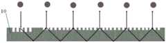
图2是本发明所述提高出射光均匀性的衍射光波导的示意图,如图2所示,所述衍射光波导10包括衍射光栅1和涂敷在衍射光栅上的折射率渐变膜2,通过不同耦出区域的折射率渐变膜2的折射率变化提高耦出光线亮度的均匀性,优选地,折射率渐变膜的折射率沿扩瞳方向变大,折射率渐变膜的折射率越大,耦出光线的亮度越大,也就是说,使得扩瞳方向前端的折射率渐变膜的折射率减低,使得扩瞳方向后端的折射率渐变膜的折射率增加,从而使得耦出光线亮度均匀。FIG. 2 is a schematic diagram of the diffractive optical waveguide for improving the uniformity of the outgoing light according to the present invention. As shown in FIG. 2 , the diffractive
在一个实施例中,折射率渐变膜2为相变材料,所述相变材料(PCM)是依靠精确控制温度(热量),使得材料在晶体和非晶体之间相互转化,得相变材料的折射率随温度阶梯变化(如图7所示,沿着扩瞳方向,折射率渐变膜的折射率呈现梯度变化,且越来越大,温度越高折射率越小,因此沿扩瞳方向,温度由高到底),提高耦出区域光线均匀性。In one embodiment, the graded
优选地,所述相变材料包括Ge2Sb2Te5(GST)。Preferably, the phase change material includes Ge2Sb2Te5 (GST).
图3是本发明所述提高出射光均匀性的衍射光波导的制造方法的流程示意图,如图3所示,所述制造方法包括:FIG. 3 is a schematic flowchart of the manufacturing method of the diffractive optical waveguide for improving the uniformity of the emitted light according to the present invention. As shown in FIG. 3 , the manufacturing method includes:
步骤S1,在衍射光栅1上镀相变材料薄膜;Step S1, coating a phase change material film on the diffraction grating 1;
步骤S2,使得相变材料薄膜的折射率按照耦出区域亮度变化而变化,获得涂覆在衍射光栅上的折射率渐变膜。In step S2, the refractive index of the phase-change material film is changed according to the change of the brightness of the out-coupling area, so as to obtain a graded refractive index film coated on the diffraction grating.
在一个实施例中,使得相变材料薄膜的折射率按照耦出区域亮度变化而变化的方法包括:通过加热方式使得相变材料薄膜的折射率随温度按照耦出区域亮度变化阶梯变化,具体地,如图4所示,包括:In one embodiment, the method for changing the refractive index of the phase-change material film according to the change of the brightness of the out-coupling area includes: making the refractive index of the phase-change material film change stepwise with the temperature according to the change of the brightness of the out-coupling area by heating, specifically , as shown in Figure 4, including:
首先在衍射光栅上镀一层相变材料薄膜21(如Ge2Sb2Te5),此时相变材料薄膜21为一个折射率均匀的薄膜;First, coat a layer of phase change material film 21 (eg Ge2Sb2Te5) on the diffraction grating, at this time the phase
然后采用制热板31加热方式,控制相变材料薄膜沿着扩瞳方向产生折射率梯度变化,从而改善耦出区域光线亮度均匀性,优选地,通过制热板31加热相变材料薄膜,通过加热器(未示出)控制不同耦出区域的制热板的温度,使得不同耦出区域的相变材料薄膜的折射率随温度不同变化,如图4所示,制热板的加热温度沿扩瞳方向(图中箭头方向)由高到底,,使得相变材料薄膜的温度沿扩瞳方向由高到低,使得相变材料薄膜的折射率沿扩瞳方向由低到高。Then, the heating method of the heating plate 31 is used to control the refractive index gradient of the phase change material film along the pupil dilation direction, so as to improve the uniformity of light brightness in the coupling-out area. Preferably, the phase change material film is heated by the heating plate 31, A heater (not shown) controls the temperature of the heating plate in different out-coupling regions, so that the refractive index of the phase-change material film in different out-coupling regions varies with temperature. As shown in Figure 4, the heating temperature of the heating plate increases along the The pupil dilation direction (arrow direction in the figure) is from high to bottom, so that the temperature of the phase change material film increases from high to low along the pupil dilation direction, so that the refractive index of the phase change material film goes from low to high along the pupil dilation direction.
在另一个实施例中,使得相变材料薄膜的折射率按照耦出区域亮度变化而变化的方法包括:通过激光照射方式使得相变材料薄膜的折射率随温度按照耦出区域亮度变化阶梯变化,具体地,如图5所示,包括:In another embodiment, the method for changing the refractive index of the phase change material film according to the change of the brightness of the out-coupling area includes: making the refractive index of the phase-change material film change stepwise according to the change of the brightness of the out-coupling area with temperature by means of laser irradiation, Specifically, as shown in Figure 5, it includes:
首先在衍射光栅上镀一层相变材料薄膜,此时相变材料薄膜为一个折射率均匀的薄膜;Firstly, a layer of phase change material film is coated on the diffraction grating, at this time, the phase change material film is a film with uniform refractive index;
然后控制激光器32的照射时间,使激光器32在不同耦出区域照射时间不同,从而使相变材料薄膜的折射率渐变,在不同耦出区域的折射率不同,优选地,通过计时器控制不同耦出区域的激光器的照射时间,从而使得相变材料薄膜的折射率随温度阶梯变化,如图5所示,激光器的照射时间沿扩瞳方向(图中箭头方向)从长到短,使得相变材料薄膜的温度沿扩瞳方向由高到低,使得相变材料薄膜的折射率沿扩瞳方向由低到高。Then, the irradiation time of the
在第三个实施例中,使得相变材料薄膜的折射率按照耦出区域亮度变化阶梯变化的方法包括:通过电激励的方式使得相变材料薄膜的折射率随温度按照耦出区域亮度变化阶梯变化,具体地,如图6所示,包括:In the third embodiment, the method for making the refractive index of the phase change material film change stepwise according to the brightness change of the out-coupling area includes: making the refractive index of the phase change material film change stepwise according to the brightness change of the out-coupling area with temperature by means of electrical excitation Variations, specifically, as shown in Figure 6, include:
首先在衍射光栅上镀一层相变材料薄膜,此时相变材料薄膜为一个折射率均匀的薄膜;Firstly, a layer of phase change material film is coated on the diffraction grating, at this time, the phase change material film is a film with uniform refractive index;
然后对不同耦出区域所对应的导电膜上施加不同强度的电压值,从而使对应耦出区域的相变材料薄膜的折射率渐变,优选地,通过电控器33对不同耦出区域的导电膜34上施加不同强度的电压值,使得导电膜具有不同的加热温度,从而使得相变材料薄膜的折射率变化,如图6所示,导电膜34上施加电压值强度沿扩瞳方向(图中箭头方向)由高到低,使得导电膜的加热温度沿扩瞳方向由高到底,从而使得相变材料薄膜的温度沿扩瞳方向由高到低,使得相变材料薄膜的折射率沿扩瞳方向由低到高。Then, voltage values of different intensities are applied to the conductive films corresponding to the different out-coupling regions, so that the refractive index of the phase-change material films corresponding to the out-coupling regions is gradually changed. Voltage values of different intensities are applied to the
在一个优选实施例中,提高出射光均匀性的衍射光波导的制造方法包括:In a preferred embodiment, the manufacturing method of the diffractive optical waveguide for improving the uniformity of the outgoing light includes:
获得相变材料薄膜,例如,Ge2Sb2Te5相变材料薄膜;Obtain a phase change material film, for example, a Ge2Sb2Te5 phase change material film;
将所述相变材料薄膜镀在衍射光栅上,此时相变材料薄膜为一个折射率均匀的薄膜;Coating the phase change material film on the diffraction grating, at this time the phase change material film is a film with a uniform refractive index;
获得相变材料薄膜的折射率随温度变化的第一曲线,相变材料随着温度的不同在非晶态和晶态之间变化,相变材料的折射率也随着温度的变化而变化,所述第一曲线通过曲线拟合的方式预先通过实验获得;Obtain the first curve of the refractive index of the phase change material film as a function of temperature. The phase change material changes between amorphous and crystalline states with temperature, and the refractive index of the phase change material also changes with temperature. The first curve is obtained through experiments in advance by means of curve fitting;
获得镀膜后衍射光波导的耦出区域的亮度变化的第二曲线,从图1中可以看出不同耦出区域的亮度不同,通过曲线模拟可以获得第二曲线;Obtain the second curve of the brightness change of the out-coupling region of the diffractive optical waveguide after coating. It can be seen from Figure 1 that the brightness of different out-coupling regions is different, and the second curve can be obtained by curve simulation;
通过第二曲线获得使得出射光线亮度均匀的沿扩瞳方向不同耦出区域的折射率变化的第三曲线,如图7所示;A third curve of the refractive index variation of different outcoupling regions along the pupil dilation direction is obtained through the second curve, which makes the brightness of the outgoing light uniform, as shown in FIG. 7 ;
通过第三曲线和第一曲线,获得不同耦出区域的温度变化的第四曲线;Through the third curve and the first curve, a fourth curve of temperature changes in different outcoupling regions is obtained;
通过第四曲线采用通过加热方式、激光照射方式或/和电激励方式控制相变材料薄膜不同耦出区域的温度,获得折射率渐变膜,例如,在非晶态时,GST的原子排布十分混乱,而在晶态时,原子排布整齐,原子排布方式的不同导致GST在红外波段的光学相纸不同,GST进行160℃以上的退火后,非晶态GST会相变为晶态的GST,晶态的GST在经过640℃高温的快速退火后,又可以回到非晶态。一旦相变完成,GST可以维持相应状态保持不变,只要没有达到相变条件,GST在常温下可以保持当前状态长达数年,也就是说,折射率渐变膜不同耦出区域的折射率可以保持数年。Through the fourth curve, the temperature of the different out-coupling regions of the phase change material film is controlled by heating, laser irradiation or/and electrical excitation to obtain a graded refractive index film. For example, in the amorphous state, the atomic arrangement of GST is very good. In the crystalline state, the atoms are arranged neatly, and the different atomic arrangements lead to different optical photo papers of GST in the infrared band. GST, the crystalline GST can return to the amorphous state after rapid annealing at a high temperature of 640 °C. Once the phase transition is completed, the GST can maintain the corresponding state unchanged. As long as the phase transition condition is not reached, the GST can maintain the current state for several years at room temperature. That is, the refractive index of the different outcoupling regions of the graded index film can Keep for several years.
采用上述制造方法获得的衍射光波导的不同耦出区域的图像的亮度如图8所示,本发明所述衍射光波导能够极高的提高出射光线均匀性。The brightness of the images of different outcoupling regions of the diffractive optical waveguide obtained by the above manufacturing method is shown in FIG. 8 , the diffractive optical waveguide of the present invention can greatly improve the uniformity of the outgoing light.
本发明还提供一种提高衍射光波导的出射光均匀性的方法,包括:The present invention also provides a method for improving the uniformity of the emitted light of the diffracted optical waveguide, comprising:
在衍射光波导耦出区域的衍射光栅上镀相变材料薄膜;Coating a phase change material film on the diffraction grating in the out-coupling area of the diffractive optical waveguide;
使得相变材料薄膜的折射率按照耦出区域亮度变化而变化,获得涂覆在衍射光栅上的折射率渐变膜。The refractive index of the phase-change material film is changed according to the change of the brightness of the out-coupling region to obtain a graded refractive index film coated on the diffraction grating.
优选地,所述使得相变材料薄膜的折射率按照耦出区域亮度变化而变化的步骤包括:Preferably, the step of changing the refractive index of the phase change material film according to the change of the brightness of the out-coupling area includes:
通过加热方式、激光照射方式或/和电激励的方式使得相变材料薄膜的折射率随温度按照耦出区域亮度变化阶梯变化。The refractive index of the phase change material film changes stepwise with temperature according to the brightness change of the coupling-out region by heating, laser irradiation or/and electrical excitation.
上述提高衍射光波导的出射光均匀性的方法提高衍射光波导成品的出光均匀性。The above method for improving the uniformity of the emitted light of the diffractive optical waveguide improves the uniformity of the emitted light of the finished diffracted optical waveguide.
本发明还提供一种头戴显示设备,包括上述各实施例的衍射光波导。The present invention also provides a head-mounted display device, including the diffractive optical waveguides of the above embodiments.
头戴显示设备可以包括一片或多片衍射光波导,当包括多片光波导时,在耦出区域的衍射光波导的衍射光栅上涂覆所述折射率渐变膜。The head-mounted display device may include one or more pieces of diffractive optical waveguides, and when multiple pieces of diffractive optical waveguides are included, the graded refractive index film is coated on the diffraction grating of the diffractive optical waveguides in the out-coupling region.
本发明提高出射光均匀性的衍射光波导及其制造方法、提高衍射光波导出射光均匀性的方法、头戴显示设备使用相变材料作为镀膜材料,然后通过对相变材料薄膜加热、激光照射或者电激励的方式使相变材料薄膜沿着光波导中光线传播方向(扩瞳方向)折射率发生渐变,从而使耦出区域的光线变得均匀,能够有效提升出射光线的均匀性。In the present invention, the diffractive optical waveguide for improving the uniformity of the outgoing light and the manufacturing method thereof, the method for improving the uniformity of the diffracted optical waveguide outgoing light, and the head-mounted display device use the phase-change material as the coating material, and then the phase-change material film is heated, irradiated with laser light or The electric excitation method makes the refractive index of the phase change material film change along the light propagation direction (pupil dilation direction) in the optical waveguide, so that the light in the coupling-out area becomes uniform, which can effectively improve the uniformity of the outgoing light.
在衍射光栅表面镀折射率渐变膜不用改变光栅的设计参数,只需要在压印之后,在衍射光栅的表面镀一层相变材料制作而成的薄膜,然后通过一定的方式,使相变材料薄膜的折射率发生梯度变化,从而有效提升耦出区域光线均匀性,并且具有价格低廉、工艺难度低、适合量产的特点。Coating the refractive index gradient film on the surface of the diffraction grating does not need to change the design parameters of the grating. It only needs to coat a film made of phase change material on the surface of the diffraction grating after embossing, and then make the phase change material in a certain way. The refractive index of the film changes gradient, which effectively improves the uniformity of light in the coupling-out area, and has the characteristics of low price, low process difficulty and suitable for mass production.
本领域技术人员应当理解,对于上述本发明所提出的提高出射光均匀性的衍射光波导及其制造方法、提高衍射光波导出射光均匀性的方法、头戴显示设备,还可以在不脱离本发明内容的基础上做出各种改进。因此,本发明的保护范围应当由所附的权利要求书的内容确定。It should be understood by those skilled in the art that the diffractive optical waveguide for improving the uniformity of the outgoing light and the method for manufacturing the same, the method for improving the uniformity of the outgoing light from the diffracted optical waveguide, and the head-mounted display device proposed by the present invention can also be used without departing from the present invention. Various improvements have been made based on the content. Therefore, the protection scope of the present invention should be determined by the contents of the appended claims.
Claims (10)
Priority Applications (1)
| Application Number | Priority Date | Filing Date | Title |
|---|---|---|---|
| CN202011185675.XACN112099141B (en) | 2020-10-29 | 2020-10-29 | Diffractive light waveguide, manufacturing method, method for improving uniformity of emitted light, and equipment |
Applications Claiming Priority (1)
| Application Number | Priority Date | Filing Date | Title |
|---|---|---|---|
| CN202011185675.XACN112099141B (en) | 2020-10-29 | 2020-10-29 | Diffractive light waveguide, manufacturing method, method for improving uniformity of emitted light, and equipment |
Publications (2)
| Publication Number | Publication Date |
|---|---|
| CN112099141Atrue CN112099141A (en) | 2020-12-18 |
| CN112099141B CN112099141B (en) | 2023-11-07 |
Family
ID=73785820
Family Applications (1)
| Application Number | Title | Priority Date | Filing Date |
|---|---|---|---|
| CN202011185675.XAActiveCN112099141B (en) | 2020-10-29 | 2020-10-29 | Diffractive light waveguide, manufacturing method, method for improving uniformity of emitted light, and equipment |
Country Status (1)
| Country | Link |
|---|---|
| CN (1) | CN112099141B (en) |
Cited By (4)
| Publication number | Priority date | Publication date | Assignee | Title |
|---|---|---|---|---|
| CN113376724A (en)* | 2021-06-21 | 2021-09-10 | 宁波舜宇奥来技术有限公司 | Method for manufacturing diffraction element |
| CN113721320A (en)* | 2021-09-06 | 2021-11-30 | 宁波舜宇奥来技术有限公司 | Optical waveguide structure and display device |
| WO2023028925A1 (en)* | 2021-09-01 | 2023-03-09 | 京东方科技集团股份有限公司 | Optical waveguide structure, ar device, and method for obtaining emergent light effect of optical waveguide structure |
| CN118444427A (en)* | 2024-07-08 | 2024-08-06 | 之江实验室 | A calibration-free non-volatile integrated silicon-based optical switch and method |
Citations (7)
| Publication number | Priority date | Publication date | Assignee | Title |
|---|---|---|---|---|
| CN1954243A (en)* | 2004-05-14 | 2007-04-25 | 住友电气工业株式会社 | Refractive index modulation diffraction optical element and projector comprising it |
| US20120044572A1 (en)* | 2009-04-20 | 2012-02-23 | Bae Systems Plc | Optical waveguides |
| CN102681066A (en)* | 2012-05-23 | 2012-09-19 | 天津大学 | High-efficient wide-angle coupling grating |
| CN107942540A (en)* | 2017-12-14 | 2018-04-20 | 中国科学院光电技术研究所 | Phase-change-material-based optical modulation device with dynamic color display and preparation method thereof |
| CN108761610A (en)* | 2018-06-13 | 2018-11-06 | 成都精密光学工程研究中心 | Regulate and control the unrelated reflective dielectric grating of polarization of film based on refractive index |
| CN109491001A (en)* | 2018-12-12 | 2019-03-19 | 成都精密光学工程研究中心 | The unrelated grating of polarization and preparation method thereof based on covering refractive index matching layers |
| CN110895357A (en)* | 2018-09-13 | 2020-03-20 | 深圳大学 | Preparation scheme of novel high-transmittance vanadium dioxide thin film element |
- 2020
- 2020-10-29CNCN202011185675.XApatent/CN112099141B/enactiveActive
Patent Citations (7)
| Publication number | Priority date | Publication date | Assignee | Title |
|---|---|---|---|---|
| CN1954243A (en)* | 2004-05-14 | 2007-04-25 | 住友电气工业株式会社 | Refractive index modulation diffraction optical element and projector comprising it |
| US20120044572A1 (en)* | 2009-04-20 | 2012-02-23 | Bae Systems Plc | Optical waveguides |
| CN102681066A (en)* | 2012-05-23 | 2012-09-19 | 天津大学 | High-efficient wide-angle coupling grating |
| CN107942540A (en)* | 2017-12-14 | 2018-04-20 | 中国科学院光电技术研究所 | Phase-change-material-based optical modulation device with dynamic color display and preparation method thereof |
| CN108761610A (en)* | 2018-06-13 | 2018-11-06 | 成都精密光学工程研究中心 | Regulate and control the unrelated reflective dielectric grating of polarization of film based on refractive index |
| CN110895357A (en)* | 2018-09-13 | 2020-03-20 | 深圳大学 | Preparation scheme of novel high-transmittance vanadium dioxide thin film element |
| CN109491001A (en)* | 2018-12-12 | 2019-03-19 | 成都精密光学工程研究中心 | The unrelated grating of polarization and preparation method thereof based on covering refractive index matching layers |
Cited By (7)
| Publication number | Priority date | Publication date | Assignee | Title |
|---|---|---|---|---|
| CN113376724A (en)* | 2021-06-21 | 2021-09-10 | 宁波舜宇奥来技术有限公司 | Method for manufacturing diffraction element |
| CN113376724B (en)* | 2021-06-21 | 2023-02-17 | 宁波舜宇奥来技术有限公司 | Method for manufacturing diffraction element |
| WO2023028925A1 (en)* | 2021-09-01 | 2023-03-09 | 京东方科技集团股份有限公司 | Optical waveguide structure, ar device, and method for obtaining emergent light effect of optical waveguide structure |
| US12222507B2 (en) | 2021-09-01 | 2025-02-11 | Beijing Boe Display Technology Co., Ltd. | Optical waveguide structure, AR device, and method for obtaining emergent light efficiency of optical waveguide structure |
| CN113721320A (en)* | 2021-09-06 | 2021-11-30 | 宁波舜宇奥来技术有限公司 | Optical waveguide structure and display device |
| CN118444427A (en)* | 2024-07-08 | 2024-08-06 | 之江实验室 | A calibration-free non-volatile integrated silicon-based optical switch and method |
| CN118444427B (en)* | 2024-07-08 | 2024-09-27 | 之江实验室 | A calibration-free non-volatile integrated silicon-based optical switch and method |
Also Published As
| Publication number | Publication date |
|---|---|
| CN112099141B (en) | 2023-11-07 |
Similar Documents
| Publication | Publication Date | Title |
|---|---|---|
| CN112099140B (en) | Diffractive optical waveguide with uniform emission brightness, manufacturing method, and head-mounted display device | |
| CN112099141B (en) | Diffractive light waveguide, manufacturing method, method for improving uniformity of emitted light, and equipment | |
| Zhang et al. | Electrically reconfigurable non-volatile metasurface using low-loss optical phase-change material | |
| Shalaginov et al. | Reconfigurable all-dielectric metalens with diffraction-limited performance | |
| Qu et al. | Thermal camouflage based on the phase-changing material GST | |
| Teo et al. | Programmable chalcogenide-based all-optical deep neural networks | |
| Michel et al. | Advanced optical programming of individual meta‐atoms beyond the effective medium approach | |
| Boyd et al. | High-efficiency metallic diffraction gratings for laser applications | |
| US11187889B2 (en) | Phase-change spatial light modulator | |
| US20220146710A1 (en) | Optical metasurfaces, and associated manufacturing methods and systems | |
| Smayev et al. | Direct single-pass writing of two-phase binary diffraction gratings in a Ge2Sb2Te5 thin film by femtosecond laser pulses | |
| CN106662677B (en) | Adaptive hot lenticule | |
| Nemati et al. | Controllable Polarization‐Insensitive and Large‐Angle Beam Switching with Phase‐Change Metasurfaces | |
| Zhao et al. | Ultrafast laser-induced integrated property–structure modulation of Ge2Sb2Te5 for multifunction and multilevel rewritable optical recording | |
| WO2024159924A1 (en) | Method for regulating optical computing device, and optical computing device | |
| WO2025123585A1 (en) | Laser processing method based on chalcogenide material, and integrated photonic device | |
| Conrads et al. | Infrared beam-shaping on demand via tailored geometric phase metasurfaces employing the plasmonic phase-change material In3SbTe2 | |
| Jiao et al. | Metasurface with all-optical tunability for spatially-resolved and multilevel thermal radiation | |
| Han et al. | 3D Femtosecond Laser Beam Deflection for High‐Precision Fabrication and Modulation of Individual Voxelated PCM Meta‐Atoms | |
| Xie et al. | Photonic Chip Based on Ultrafast Laser-Induced Reversible Phase Change for Convolutional Neural Network | |
| CN116540377B (en) | On-chip integrated superlens with electric control zooming function | |
| Kang et al. | Scalable laser-written Ge-As-Pb-Se chalcogenide glass-ceramic films and the realization of infrared gradient refractive index elements | |
| CN108732672A (en) | Optical filter structure, preparation method thereof and adjustment method of transmission characteristic | |
| CN118393620A (en) | Preparation method of reconfigurable phase-change material super-surface device and reconfigurable phase-change material super-surface device | |
| JP4793011B2 (en) | Antireflection film forming method |
Legal Events
| Date | Code | Title | Description |
|---|---|---|---|
| PB01 | Publication | ||
| PB01 | Publication | ||
| SE01 | Entry into force of request for substantive examination | ||
| SE01 | Entry into force of request for substantive examination | ||
| TA01 | Transfer of patent application right | ||
| TA01 | Transfer of patent application right | Effective date of registration:20221117 Address after:261000 north of Yuqing street, east of Dongming Road, high tech Zone, Weicheng District, Weifang City, Shandong Province (Room 502, Geer electronic office building) Applicant after:GoerTek Optical Technology Co.,Ltd. Address before:261031 No. 268 Dongfang Road, hi tech Industrial Development Zone, Shandong, Weifang Applicant before:GOERTEK Inc. | |
| GR01 | Patent grant | ||
| GR01 | Patent grant |