CN112083568A - Augmented reality display device and augmented reality glasses - Google Patents
Augmented reality display device and augmented reality glassesDownload PDFInfo
- Publication number
- CN112083568A CN112083568ACN201910512591.3ACN201910512591ACN112083568ACN 112083568 ACN112083568 ACN 112083568ACN 201910512591 ACN201910512591 ACN 201910512591ACN 112083568 ACN112083568 ACN 112083568A
- Authority
- CN
- China
- Prior art keywords
- coupling
- light
- augmented reality
- structural
- display device
- Prior art date
- Legal status (The legal status is an assumption and is not a legal conclusion. Google has not performed a legal analysis and makes no representation as to the accuracy of the status listed.)
- Pending
Links
- 230000003190augmentative effectEffects0.000titleclaimsabstractdescription46
- 239000011521glassSubstances0.000titleclaimsabstractdescription21
- 239000002086nanomaterialSubstances0.000claimsabstractdescription12
- 238000003384imaging methodMethods0.000claimsabstractdescription11
- 238000010168coupling processMethods0.000claimsdescription22
- 238000005859coupling reactionMethods0.000claimsdescription22
- 230000008878couplingEffects0.000claimsdescription8
- 239000011449brickSubstances0.000claimsdescription5
- 108010001267Protein SubunitsProteins0.000claimsdescription4
- 102000002067Protein SubunitsHuman genes0.000claimsdescription2
- 238000010586diagramMethods0.000description20
- 239000010408filmSubstances0.000description20
- 238000005516engineering processMethods0.000description5
- 239000010409thin filmSubstances0.000description5
- 239000004973liquid crystal related substanceSubstances0.000description4
- 230000003287optical effectEffects0.000description4
- 239000002356single layerSubstances0.000description4
- 238000000206photolithographyMethods0.000description3
- 230000005540biological transmissionEffects0.000description2
- 239000010410layerSubstances0.000description2
- 239000000463materialSubstances0.000description2
- 238000000034methodMethods0.000description2
- 238000012986modificationMethods0.000description2
- 230000004048modificationEffects0.000description2
- 229920002120photoresistant polymerPolymers0.000description2
- 239000011347resinSubstances0.000description2
- 229920005989resinPolymers0.000description2
- 239000012141concentrateSubstances0.000description1
- 239000006185dispersionSubstances0.000description1
- 230000004927fusionEffects0.000description1
- 230000008569processEffects0.000description1
- 210000001747pupilAnatomy0.000description1
- 230000010076replicationEffects0.000description1
- 229910052710siliconInorganic materials0.000description1
- 239000010703siliconSubstances0.000description1
Images


Classifications
- G—PHYSICS
- G02—OPTICS
- G02B—OPTICAL ELEMENTS, SYSTEMS OR APPARATUS
- G02B27/00—Optical systems or apparatus not provided for by any of the groups G02B1/00 - G02B26/00, G02B30/00
- G02B27/01—Head-up displays
- G02B27/0101—Head-up displays characterised by optical features
- G—PHYSICS
- G02—OPTICS
- G02B—OPTICAL ELEMENTS, SYSTEMS OR APPARATUS
- G02B27/00—Optical systems or apparatus not provided for by any of the groups G02B1/00 - G02B26/00, G02B30/00
- G02B27/01—Head-up displays
- G02B27/017—Head mounted
- G02B27/0172—Head mounted characterised by optical features
- G—PHYSICS
- G02—OPTICS
- G02B—OPTICAL ELEMENTS, SYSTEMS OR APPARATUS
- G02B27/00—Optical systems or apparatus not provided for by any of the groups G02B1/00 - G02B26/00, G02B30/00
- G02B27/01—Head-up displays
- G02B27/017—Head mounted
- G02B2027/0178—Eyeglass type
Landscapes
- Physics & Mathematics (AREA)
- General Physics & Mathematics (AREA)
- Optics & Photonics (AREA)
- Optical Couplings Of Light Guides (AREA)
Abstract
Translated fromChinese
Description
Translated fromChinese技术领域technical field
本发明涉及投影显示技术领域,特别涉及一种增强现实显示装置及增强现实眼镜。The present invention relates to the technical field of projection display, in particular to an augmented reality display device and augmented reality glasses.
背景技术Background technique
1990年波音公司创造了增强现实,随后越来越多的研究所、企业及高校对增强现实展开研究,如微软推出的Hololens全息眼镜、Google Glass,联想推出的New Glass等。增强现实的近眼显示在一只眼睛或两只眼睛的视野范围内创建虚拟图像,使虚拟图像与现实景象融合、交互。传统的光学波导元件耦合图像光进入人眼,包括使用棱镜、反射镜、半透半反光波导、全息及衍射光栅。波导显示系统是利用全反射原理实现光波传输,结合衍射元件,实现光线的定向传导,进而将图像光导向人眼,使用户可以看到投影的图像。In 1990, Boeing created augmented reality, and then more and more research institutes, enterprises and universities conducted research on augmented reality, such as Microsoft's Hololens holographic glasses, Google Glass, and Lenovo's New Glass. Augmented reality's near-eye display creates a virtual image within the field of view of one or both eyes, allowing the virtual image to merge and interact with the real scene. Conventional optical waveguide elements couple image light into the human eye, including the use of prisms, mirrors, transflective waveguides, holograms, and diffraction gratings. The waveguide display system uses the principle of total reflection to realize light wave transmission, combined with diffractive elements to realize the directional transmission of light, and then guide the image light to the human eye, so that the user can see the projected image.
专利WO2009059446A1,公开了一种眼镜式显示装置,包括微显示芯片、对微显示芯片产生的图像进行放大处理的光学透镜组、以及将光学透镜组输出的光线传送到眼镜的光传导平板,提供了一种具有较大视场、较大出瞳尺寸的眼睛式显示装置。Patent WO2009059446A1 discloses a glasses-type display device, including a micro-display chip, an optical lens group for amplifying an image generated by the micro-display chip, and a light-conducting flat plate for transmitting the light output from the optical lens group to the glasses, providing An eye-type display device with larger field of view and larger exit pupil size.
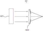
图1是现有的投影系统的结构示意图。如图1所示,投影系统包括光源71和透镜72,光源71发出的光经过透镜72后聚焦成像。透镜72为平凸透镜,透镜72由玻璃或树脂材料制成,该透镜72的尺度为毫米级。因此,现有的投影系统以及应用该投影系统的增强现实显示装置体积及重量比较大,庞大的投影系统阻碍了用户的体验度,无法带来观看舒适性。FIG. 1 is a schematic structural diagram of a conventional projection system. As shown in FIG. 1 , the projection system includes a
发明内容SUMMARY OF THE INVENTION
有鉴于此,本发明提供一种增强现实显示装置,减小了微投系统的体积与重量,提高了用户舒适性。In view of this, the present invention provides an augmented reality display device, which reduces the volume and weight of the micro-projection system and improves user comfort.
一种增强现实显示装置,包括微投系统和纳米波导镜片,微投系统设置于纳米波导镜片的上方,微投系统包括光源和功能薄膜,功能薄膜上设有聚焦成像的纳米结构,光源发出的光经过功能薄膜后聚焦成像,图像光由纳米波导镜片输出。An augmented reality display device includes a micro-projection system and a nano-waveguide lens, the micro-projection system is arranged above the nano-waveguide lens, the micro-projection system includes a light source and a functional film, the functional film is provided with a nanostructure for focusing imaging, and the light source emits The light is focused and imaged after passing through the functional film, and the image light is output by the nano-waveguide lens.
在本发明的实施例中,上述功能薄膜为菲尼尔透镜。In the embodiment of the present invention, the above-mentioned functional film is a Fresnel lens.
在本发明的实施例中,上述功能薄膜为纳米砖。In an embodiment of the present invention, the above-mentioned functional film is a nano-brick.
在本发明的实施例中,上述纳米波导镜片包括波导片本体,该波导片本体的表面设有耦入区域和耦出区域,该耦入区域和该耦出区域内均设有多个结构单元像素,各该结构单元像素包括第一结构子单元、第二结构子单元和第三结构子单元;In an embodiment of the present invention, the above-mentioned nano-waveguide sheet includes a waveguide sheet body, and a surface of the waveguide sheet body is provided with a coupling-in region and a coupling-out region, and a plurality of structural units are provided in the coupling-in region and the coupling-out region. a pixel, each of the structural unit pixels includes a first structural subunit, a second structural subunit and a third structural subunit;
当图像光入射至该耦入区域时,红光可从该耦入区域的第一结构子单元进入该波导片本体内,蓝光和绿光无法从该第一结构子单元进入该波导片本体内,红光在该波导片本体内全反射至该耦出区域,并从该耦出区域的第一结构子单元射出;When the image light is incident on the coupling-in area, red light can enter the waveguide sheet body from the first structural sub-unit in the coupling-in area, and blue light and green light cannot enter the waveguide sheet body from the first structural sub-unit , the red light is totally reflected to the out-coupling area in the body of the waveguide sheet, and is emitted from the first structural subunit of the out-coupling area;
蓝光可从该耦入区域的第二结构子单元进入该波导片本体内,红光和绿光无法从该第二结构子单元进入该波导片本体内,蓝光在该波导片本体内全反射至该耦出区域,并可从该耦出区域的第二结构子单元射出;Blue light can enter the waveguide sheet body from the second structural sub-unit in the coupling-in area, red light and green light cannot enter the waveguide sheet body from the second structural sub-unit, and blue light is totally reflected in the waveguide sheet body. The coupling-out region can be emitted from the second structural subunit of the coupling-out region;
绿光可从该耦入区域的第三结构子单元进入该波导片本体内,蓝光和红光无法从该耦入区域的第三结构子单元进入该波导片本体内,绿光在该波导片本体内全反射至该耦出区域,并可从该耦出区域的第三结构子单元射出。Green light can enter the waveguide sheet body from the third structural subunit in the coupling-in area, blue light and red light cannot enter the waveguide sheet body from the third structural subunit in the coupling-in area, and green light is in the waveguide sheet. The body is totally reflected to the coupling-out region, and can be emitted from the third structural subunit of the coupling-out region.
在本发明的实施例中,上述第一结构子单元包括多个第一衍射光栅,该第二结构子单元包括多个第二衍射光栅,该第三结构子单元包括多个第三衍射光栅。In an embodiment of the present invention, the first structural subunit includes a plurality of first diffraction gratings, the second structural subunit includes a plurality of second diffraction gratings, and the third structural subunit includes a plurality of third diffraction gratings.
在本发明的实施例中,上述第一衍射光栅的周期与红光的波长匹配;该第二衍射光栅的周期与蓝光的波长匹配;该第三衍射光栅的周期与绿光的波长匹配。In the embodiment of the present invention, the period of the first diffraction grating matches the wavelength of red light; the period of the second diffraction grating matches the wavelength of blue light; the period of the third diffraction grating matches the wavelength of green light.
在本发明的实施例中,上述各该第一衍射光栅倾斜设置;各该第二衍射光栅倾斜设置;各该第三衍射光栅倾斜设置。In the embodiment of the present invention, each of the first diffraction gratings is arranged obliquely; each of the second diffraction gratings is arranged obliquely; and each of the third diffraction gratings is arranged obliquely.
在本发明的实施例中,上述波导片本体的表面还设有转折区域,该转折区域内设有多个该结构单元像素,当图像光入射至该耦入区域时,图像光在该波导片本体内全反射至该转折区域,该转折区域改变图像光的传播方向,使改变方向后的图像光全反射至该耦出区域。In the embodiment of the present invention, the surface of the waveguide sheet body is further provided with a turning area, and a plurality of the structural unit pixels are arranged in the turning area. The body is totally reflected to the inflection area, and the inflection area changes the propagation direction of the image light, so that the changed direction of the image light is totally reflected to the outcoupling area.
在本发明的实施例中,上述纳米波导镜片的折射率为1.3~2.2。In the embodiment of the present invention, the refractive index of the nano-waveguide sheet is 1.3-2.2.
本发明还提供一种增强现实眼镜,包括上述的增强现实显示装置,该增强现实眼镜还包括框架和支撑腿,该支撑腿的一端连接在该框架上,该框架上设置有两块纳米波导镜片,该支撑腿上设置有微投系统。The present invention also provides augmented reality glasses, including the augmented reality display device described above, the augmented reality glasses further comprising a frame and a support leg, one end of the support leg is connected to the frame, and two nano-waveguide lenses are arranged on the frame , the support leg is provided with a micro-projection system.
本发明的增强现实显示装置的微投系统设置于纳米波导镜片的上方,微投系统包括光源和功能薄膜,功能薄膜上设有聚焦成像的纳米结构,光源发出的光经过功能薄膜后聚焦成像,图像光由纳米波导镜片输出。本发明的增强现实显示装置通过功能薄膜便可以实现多组透镜的成像功能,减小了微投系统的体积与重量,提高了用户舒适性。The micro-projection system of the augmented reality display device of the present invention is arranged above the nano-waveguide lens. The micro-projection system includes a light source and a functional film. The functional film is provided with a nanostructure for focusing imaging. The light emitted by the light source passes through the functional film and is focused and imaging. The image light is output by the nano-waveguide lens. The augmented reality display device of the present invention can realize the imaging function of multiple groups of lenses through the functional film, thereby reducing the volume and weight of the micro-projection system and improving the comfort of users.
附图说明Description of drawings
图1是现有的投影系统的结构示意图。FIG. 1 is a schematic structural diagram of a conventional projection system.
图2a是本发明的纳米波导镜片的俯视结构示意图。Fig. 2a is a schematic top view of the structure of the nano-waveguide lens of the present invention.
图2b是图2a所示的纳米波导镜片的剖视结构示意图。FIG. 2b is a schematic cross-sectional structural diagram of the nano-waveguide lens shown in FIG. 2a.
图3a至图3c是本发明的结构单元像素在波导片本体上排布状态的示意图。3a to 3c are schematic diagrams showing the arrangement state of the structural unit pixels of the present invention on the waveguide sheet body.
图4是本发明的三维显示装置的结构示意图。FIG. 4 is a schematic structural diagram of the three-dimensional display device of the present invention.
图5是本发明的眼镜的结构示意图。FIG. 5 is a schematic structural diagram of the glasses of the present invention.
图6是本发明的增强现实显示装置的结构示意图。FIG. 6 is a schematic structural diagram of an augmented reality display device of the present invention.
图7是本发明第四实施例的微投系统的工作时的结构示意图。FIG. 7 is a schematic structural diagram of the micro-projection system in operation according to the fourth embodiment of the present invention.
图8是本发明第五实施例的微投系统的工作时的结构示意图。FIG. 8 is a schematic structural diagram of the micro-projection system in operation according to the fifth embodiment of the present invention.
图9是本发明第六实施例的纳米波导镜片的结构示意图。FIG. 9 is a schematic structural diagram of a nano-waveguide lens according to a sixth embodiment of the present invention.
图10是本发明的增强现实眼镜的结构示意图。FIG. 10 is a schematic structural diagram of the augmented reality glasses of the present invention.
具体实施方式Detailed ways
为使本发明的目的、技术方案和优点更加清楚,下面将结合附图对本发明的实施方式作进一步地描述。In order to make the objectives, technical solutions and advantages of the present invention clearer, the embodiments of the present invention will be further described below with reference to the accompanying drawings.
第一实施例first embodiment
图2a是本发明的纳米波导镜片的俯视结构示意图。图2b是图2a所示的纳米波导镜片的剖视结构示意图。如图2a和图2b所示,纳米波导镜片10包括波导片本体11。波导片本体11的表面设有耦入区域11a和耦出区域11b。波导片本体11具有相对的第一表面101和第二表面102,第一表面101或第二表面102上,优选地,波导片本体11的第一表面101设有耦入区域11a和耦出区域11b,且耦入区域11a与耦出区域11b相互间隔设置。耦入区域11a和耦出区域11b内均设有多个结构单元像素12,各结构单元像素12包括第一结构子单元12a、第二结构子单元12b和第三结构子单元12c。在本实施例中,耦入区域11a和耦出区域11b的形状为圆形、矩形或锥形,但并不以此为限。Fig. 2a is a schematic top view of the structure of the nano-waveguide lens of the present invention. FIG. 2b is a schematic cross-sectional structural diagram of the nano-waveguide lens shown in FIG. 2a. As shown in FIGS. 2 a and 2 b , the nano-
进一步地,第一结构子单元12a包括多个第一衍射光栅121,第一衍射光栅121的周期与红光的波长匹配。第二结构子单元12b包括多个第二衍射光栅122,第二衍射光栅122的周期与蓝光的波长匹配。第三结构子单元12c包括多个第三衍射光栅123,第三衍射光栅123的周期与绿光的波长匹配。在本实施例中,第一衍射光栅121、第二衍射光栅122和第三衍射光栅123的周期和取向角满足光栅方程,具体满足方程式(1)和(2):Further, the first
tanψ=sinφ/(cosφ-n sinθ1(Λ/λ)) (1)tanψ=sinφ/(cosφ-n sinθ1 (Λ/λ)) (1)
其中,ψ表示衍射光的方位角;φ表示衍射光栅的取向角;θ1表示入射光的入射角;Λ表示衍射光栅的周期;λ表示入射光的波长;n表示衍射光栅的折射率;Among them, ψ represents the azimuth angle of the diffracted light; φ represents the orientation angle of the diffraction grating; θ1 represents the incident angle of the incident light; Λ represents the period of the diffraction grating; λ represents the wavelength of the incident light; n represents the refractive index of the diffraction grating;
sin2(θ2)=(λ/Λ)2+(n sinθ1)2+2n sinθ1cosφ(λ/Λ) (2)sin2 (θ2 )=(λ/Λ)2 +(n sinθ1 )2 +2n sinθ1 cosφ(λ/Λ) (2)
其中,θ2表示衍射光的衍射角。Here, θ2 represents the diffraction angle of diffracted light.
当规定好入射光线波长、入射角以及衍射光线衍射角和衍射方位角之后,就可以通过上述两个公式计算出所需的第一衍射光栅121、第二衍射光栅122和第三衍射光栅123的周期和取向角,具体计算过程请参照现有技术,此处不再赘述。After the wavelength of the incident light, the incident angle, the diffraction angle and the diffraction azimuth angle of the diffracted light are specified, the required diffraction gratings of the
当图像光入射至耦入区域11a时,红光可从耦入区域11a的第一结构子单元12a进入波导片本体11内,蓝光和绿光无法从第一结构子单元12a进入波导片本体11内,红光在波导片本体11内全反射至耦出区域11b,并从耦出区域11b的第一结构子单元12a射出;When the image light is incident on the coupling-in
蓝光可从耦入区域11a的第二结构子单元12b进入波导片本体11内,红光和绿光无法从第二结构子单元12b进入波导片本体11内,蓝光在波导片本体11内全反射至耦出区域11b,并可从耦出区域11b的第二结构子单元12b射出;Blue light can enter the
绿光可从耦入区域11a的第三结构子单元12c进入波导片本体11内,蓝光和红光无法从耦入区域11a的第三结构子单元12c进入波导片本体11内,绿光在波导片本体11内全反射至耦出区域11b,并可从耦出区域11b的第三结构子单元12c射出,当红光、蓝光和绿光从耦出区域11b射出耦合后形成彩色图像。Green light can enter the
图3a至图3c是本发明的结构单元像素在波导片本体上排布状态的示意图。如图3a至图3c所示,各第一衍射光栅121倾斜设置;各第二衍射光栅122倾斜设置;各第三衍射光栅123倾斜设置,且第一衍射光栅121、第二衍射光栅122和第三衍射光栅123的倾斜方向一致,倾斜设置的衍射光栅对波长具有选择性,避免色散,针对某一波段具有较高的衍射效率,例如红光可从耦入区域11a的第一结构子单元12a进入波导片本体11内、蓝光可从耦入区域11a的第二结构子单元12b进入波导片本体11内、绿光可从耦入区域11a的第三结构子单元12c进入波导片本体11内。在本实施例中,第一衍射光栅121、第二衍射光栅122和第三衍射光栅123可采用全息干涉技术、光刻技术或纳米压印技术制备而成,根据实际需要可自由选择。3a to 3c are schematic diagrams showing the arrangement state of the structural unit pixels of the present invention on the waveguide sheet body. As shown in FIGS. 3 a to 3 c , each of the
各结构单元像素12的第一结构子单元12a、第二结构子单元12b和第三结构子单元12c的排布位置可根据实际需要自由选择,保证第一衍射光栅121、第二衍射光栅122和第三衍射光栅123处于倾斜状态即可。例如:第一结构子单元12a、第二结构子单元12b和第三结构子单元12c沿着波导片本体11的长度方向或宽度方向依次设置,如图3a所示。例如:第一结构子单元12a沿着波导片本体11的长度方向或宽度方向依次设置,第二结构子单元12b和第三结构子单元12c位于第一结构子单元12a的一侧,且第二结构子单元12b和第三结构子单元12c沿着波导片本体11的长度方向或宽度方向依次设置,如图3b所示。例如:第一结构子单元12a设置于第二结构子单元12b之间第三结构子单元12c之间,第二结构子单元12b、第一结构子单元12a和第三结构子单元12c依次倾斜设置,如图3c所示。The arrangement positions of the first
进一步地,各结构单元像素12的尺寸为5~200μm。Further, the size of each
进一步地,波导片本体11为单层结构,彩色图像光经过耦入区域11a时形成红光、蓝光和绿光单色光进入导波片11,红光、蓝光和绿光在单层波导片本体11内发生全反射,且光线相互不干扰,红光、蓝光和绿光从耦出区域11b输出耦合形成彩色图像。波导片本体11的耦入区域11a和耦出区域11b分别设置多个分别对红光、蓝光和绿光进行衍射的结构单元像素12,充分利用空间资源通过单层镜片上的多个结构子单元实现多种波段光的有序传导。在不增加镜片的情况下,可以大幅缩小显示系统或装置的体积、质量,具有明显的轻薄化优势。Further, the
第二实施例Second Embodiment
本发明还涉及一种三维显示装置,三维显示装置包括上述的纳米波导镜片10。The present invention also relates to a three-dimensional display device, which includes the above-mentioned nano-
图4是本发明的三维显示装置的结构示意图。如图4所示,三维显示装置20还包括显示装置21和透镜22。显示装置21位于纳米波导镜片10的上方,透镜22设置于显示装置21与纳米波导镜片10之间,显示装置21发出的图像光经过透镜22后入射至纳米波导镜片10的耦入区域11a。在本实施例中,透镜22为平凸透镜,透镜22由玻璃或树脂材料制成,该透镜22的尺度为毫米级。FIG. 4 is a schematic structural diagram of the three-dimensional display device of the present invention. As shown in FIG. 4 , the three-
第三实施例Third Embodiment
本发明还涉及一种眼镜,眼镜包括上述的纳米波导镜片10。The present invention also relates to glasses, which include the aforementioned nano-
图5是本发明的眼镜的结构示意图。如图5所示,眼镜30还包括镜框31和镜腿32。镜腿32的一端连接在镜框31上,镜框31上设有两块纳米波导镜片10,两块纳米波导镜片10的耦出区域11b与人眼对应设置,耦入区域11a与镜腿32对应设置。在本实施例中,镜腿32与镜框31连接的端部设有容置腔,容置腔正对纳米波导镜片10的耦入区域11a,该容置腔内安装有显示屏(图未示)和DMD数字微镜阵列(图未示)。显示屏出射图像光,经过透镜组聚焦,图像光耦合至波导片本体11的耦入区域11a,经过各结构单元像素12的第一结构子单元12a、第二结构子单元12b和第三结构子单元12c传输至耦出区域11b,并从耦出区域11b输出至人眼,人眼接收来自纳米波导镜片10的耦合图像光,利用双眼视差,实现三维彩色显示。FIG. 5 is a schematic structural diagram of the glasses of the present invention. As shown in FIG. 5 , the
第四实施例Fourth Embodiment
本发明还涉及一种增强现实显示装置,增强现实显示装置包括上述的纳米波导镜片10。The present invention also relates to an augmented reality display device, the augmented reality display device includes the above-mentioned nano-
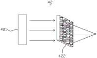
图6是本发明的增强现实显示装置的结构示意图。如图6所示,增强现实显示装置40包括微投系统42和纳米波导镜片10。微投系统42设置于纳米波导镜片10的上方,微投系统42包括光源421和功能薄膜422,功能薄膜422上设有聚焦成像的纳米结构,光源发出的光经过功能薄膜422后聚焦成像,图像光由纳米波导镜片10输出。在本实施例中,功能薄膜422可热变形,也可由光刻胶制成,在其他实施例中,功能薄膜422的纳米结构是通过复制转印形成的结构。FIG. 6 is a schematic structural diagram of an augmented reality display device of the present invention. As shown in FIG. 6 , the augmented
进一步地,微投系统42的光源可选自液晶投影机(Liquid Crystal on Silicon;LCOS)、投影仪(Digital Light Procession;DLP)、液晶显示器(Liquid Crystal Display;LCD)、发光二极管(LED)其中之一。Further, the light source of the
进一步地,纳米波导镜片10可以为第一实施例所述的单层结构,但并不以此为限,纳米波导镜片10也可为多层结构,优选地,纳米波导镜片10包括三片波导片本体12,三片波导片本体12堆叠设置,上层的波导片本体12的表面设有多个第一结构子单元12a,中层的波导片本体12的表面设有多个第二结构子单元12b,下层的波导片本体12的表面设有多个第三结构子单元12c,关于第一结构子单元12a、第二结构子单元12b和第三结构子单元12c的结构和功能请参照第一实施例,此处不再赘述。纳米波导镜片10的折射率为1.3~2.2。Further, the nano-
在本实施例中,功能薄膜422为菲尼尔透镜,仅通过功能薄膜422便可以实现多组透镜的成像功能,减小了微投系统42的体积与重量,提高了用户舒适性。In this embodiment, the
图7是本发明第四实施例的微投系统的工作时的结构示意图。如图7所示,功能薄膜422表面的纳米结构为一系列锯齿型凹槽组成,功能薄膜422的中心区域的表面为椭圆弧面,从功能薄膜422的中心区域向边缘方向,各凹槽的角度不同,但每个凹槽将光线集中一处,形成中心焦点,每个凹槽都可以看做一个独立的小透镜,把光线调整成平面光或聚光,这些凹槽均是采用光刻技术制作的纳米结构,因此纳米结构的尺度可以为纳米级,能极大压缩微投系统42的体积和重量。FIG. 7 is a schematic structural diagram of the micro-projection system in operation according to the fourth embodiment of the present invention. As shown in FIG. 7 , the nanostructures on the surface of the functional
第五实施例Fifth Embodiment
图8是本发明第五实施例的微投系统的工作时的结构示意图。如图8所示,本实施例的增强现实显示装置40结构与第四实施例的增强现实显示装置40结构大致相同,不同点在于微投系统42结构不同。在本实施例中,功能薄膜422为纳米砖,仅通过功能薄膜422便可以实现多组透镜的成像功能,减小了微投系统42的体积与重量,提高了用户舒适性。FIG. 8 is a schematic structural diagram of the micro-projection system in operation according to the fifth embodiment of the present invention. As shown in FIG. 8 , the structure of the augmented
如图8所示,功能薄膜422的表面无序排布有多个纳米砖,使得功能薄膜422可以在平面上实现几何透镜的光学聚焦功能,这些纳米砖均是采用光刻技术制作的纳米结构,因此纳米结构的尺度可以为纳米级,能极大压缩微投系统42的体积和重量。As shown in FIG. 8 , a plurality of nano-bricks are randomly arranged on the surface of the
第六实施例Sixth Embodiment
图9是本发明第六实施例的纳米波导镜片的结构示意图。如图9所示,本实施例的增强现实显示装置40结构与第四实施例的增强现实显示装置40结构大致相同,不同点在于纳米波导镜片10结构不同。FIG. 9 is a schematic structural diagram of a nano-waveguide lens according to a sixth embodiment of the present invention. As shown in FIG. 9 , the structure of the augmented
具体地,如图9所示,波导片本体11的表面还设有转折区域11c,转折区域11c内设有多个结构单元像素12,各结构单元像素12包括第一结构子单元12a、第二结构子单元12b和第三结构子单元12c,关于结构单元像素12的功能和作用请参照第一实施例,此处不再赘述。当图像光入射至耦入区域11a时,图像光在波导片本体11内全反射至转折区域11c,转折区域11c改变图像光的传播方向,使改变方向后的图像光全反射至耦出区域11b。在本实施例中,微投系统42出射的光线入射至纳米波导镜片10,光线经过弯折后出射至人眼,用户透过纳米波导镜片10在一定位置便可以看到所呈现的图像,实现虚实融合。纳米波导镜片10的转折区域11c改变了光线的传播方向,扩大了视角范围,更能满足用户需求。Specifically, as shown in FIG. 9 , the surface of the
第七实施例Seventh Embodiment
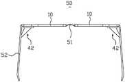
本发明还涉及一种增强现实眼镜,增强现实眼镜包括上述的增强现实显示装置40。The present invention also relates to augmented reality glasses, which include the augmented
图10是本发明的增强现实眼镜的结构示意图。如图10所示,增强现实眼镜50还包括框架51和支撑腿52,支撑腿52的一端连接在框架51上,框架51上设置有两块纳米波导镜片10,支撑腿52上设置有微投系统42。在本实施例中,左、右两个独立的微投系统42输出不同视差图像,从而实现立体三维显示。FIG. 10 is a schematic structural diagram of the augmented reality glasses of the present invention. As shown in FIG. 10 , the
本发明的增强现实显示装置40的微投系统42设置于纳米波导镜片10的上方,微投系统42包括光源421和由光刻胶制成的功能薄膜422,功能薄膜422上设有聚焦成像的纳米结构,光源421发出的光经过功能薄膜422后聚焦成像,图像光由纳米波导镜片10输出。本发明的增强现实显示装置40通过功能薄膜422便可以实现多组透镜的成像功能,减小了微投系统42的体积与重量,提高了用户舒适性。The
本发明并不限于上述实施方式中的具体细节,在本发明的技术构思范围内,可以对本发明的技术方案进行多种简单变型,这些简单变型均属于本发明的保护范围。在上述具体实施方式中所描述的各个具体技术特征,在不矛盾的情况下,可以通过任何合适的方式进行组合。为了避免不必要的重复,本发明对各种可能的组合方式不再另行说明。The present invention is not limited to the specific details in the above-mentioned embodiments, and within the scope of the technical concept of the present invention, various simple modifications can be made to the technical solutions of the present invention, and these simple modifications all belong to the protection scope of the present invention. The various specific technical features described in the above-mentioned specific embodiments may be combined in any suitable manner under the condition of no contradiction. In order to avoid unnecessary repetition, the present invention will not further describe various possible combinations.
Claims (10)
Translated fromChinesePriority Applications (1)
| Application Number | Priority Date | Filing Date | Title |
|---|---|---|---|
| CN201910512591.3ACN112083568A (en) | 2019-06-13 | 2019-06-13 | Augmented reality display device and augmented reality glasses |
Applications Claiming Priority (1)
| Application Number | Priority Date | Filing Date | Title |
|---|---|---|---|
| CN201910512591.3ACN112083568A (en) | 2019-06-13 | 2019-06-13 | Augmented reality display device and augmented reality glasses |
Publications (1)
| Publication Number | Publication Date |
|---|---|
| CN112083568Atrue CN112083568A (en) | 2020-12-15 |
Family
ID=73734522
Family Applications (1)
| Application Number | Title | Priority Date | Filing Date |
|---|---|---|---|
| CN201910512591.3APendingCN112083568A (en) | 2019-06-13 | 2019-06-13 | Augmented reality display device and augmented reality glasses |
Country Status (1)
| Country | Link |
|---|---|
| CN (1) | CN112083568A (en) |
Cited By (4)
| Publication number | Priority date | Publication date | Assignee | Title |
|---|---|---|---|---|
| CN113359300A (en)* | 2021-06-21 | 2021-09-07 | 北京亮亮视野科技有限公司 | Thin film type near-to-eye display system and glasses with built-in display system |
| CN114527573A (en)* | 2022-02-28 | 2022-05-24 | 舜宇奥来半导体光电(上海)有限公司 | Optical waveguide assembly and near-eye display device |
| CN114779397A (en)* | 2022-04-29 | 2022-07-22 | 北京枭龙科技有限公司 | Single-layer grating waveguide device for realizing color display and near-to-eye display device |
| CN116774334A (en)* | 2023-06-30 | 2023-09-19 | 天津大学四川创新研究院 | Curved period nano grating optical waveguide chip and application thereof |
Citations (7)
| Publication number | Priority date | Publication date | Assignee | Title |
|---|---|---|---|---|
| CN102122060A (en)* | 2010-01-07 | 2011-07-13 | 颖台科技股份有限公司 | Compound Concentrating Device |
| CN102445830A (en)* | 2010-10-05 | 2012-05-09 | 江国庆 | Color image projection device and image projection method thereof |
| CN106338832A (en)* | 2016-11-09 | 2017-01-18 | 苏州苏大维格光电科技股份有限公司 | Single holographic diffraction optical waveguide lens and 3D display device |
| CN106646890A (en)* | 2017-03-10 | 2017-05-10 | 京东方科技集团股份有限公司 | Virtual reality display device and manufacturing method thereof |
| CN106773057A (en)* | 2017-01-13 | 2017-05-31 | 苏州苏大维格光电科技股份有限公司 | A kind of monolithic hologram diffraction waveguide three-dimensional display apparatus |
| CN109196387A (en)* | 2016-04-05 | 2019-01-11 | 哈佛学院院长及董事 | Super lens for subwavelength resolution imaging |
| CN109752905A (en)* | 2017-11-08 | 2019-05-14 | 三星电子株式会社 | Projectors including metalens |
- 2019
- 2019-06-13CNCN201910512591.3Apatent/CN112083568A/enactivePending
Patent Citations (7)
| Publication number | Priority date | Publication date | Assignee | Title |
|---|---|---|---|---|
| CN102122060A (en)* | 2010-01-07 | 2011-07-13 | 颖台科技股份有限公司 | Compound Concentrating Device |
| CN102445830A (en)* | 2010-10-05 | 2012-05-09 | 江国庆 | Color image projection device and image projection method thereof |
| CN109196387A (en)* | 2016-04-05 | 2019-01-11 | 哈佛学院院长及董事 | Super lens for subwavelength resolution imaging |
| CN106338832A (en)* | 2016-11-09 | 2017-01-18 | 苏州苏大维格光电科技股份有限公司 | Single holographic diffraction optical waveguide lens and 3D display device |
| CN106773057A (en)* | 2017-01-13 | 2017-05-31 | 苏州苏大维格光电科技股份有限公司 | A kind of monolithic hologram diffraction waveguide three-dimensional display apparatus |
| CN106646890A (en)* | 2017-03-10 | 2017-05-10 | 京东方科技集团股份有限公司 | Virtual reality display device and manufacturing method thereof |
| CN109752905A (en)* | 2017-11-08 | 2019-05-14 | 三星电子株式会社 | Projectors including metalens |
Cited By (5)
| Publication number | Priority date | Publication date | Assignee | Title |
|---|---|---|---|---|
| CN113359300A (en)* | 2021-06-21 | 2021-09-07 | 北京亮亮视野科技有限公司 | Thin film type near-to-eye display system and glasses with built-in display system |
| CN114527573A (en)* | 2022-02-28 | 2022-05-24 | 舜宇奥来半导体光电(上海)有限公司 | Optical waveguide assembly and near-eye display device |
| CN114779397A (en)* | 2022-04-29 | 2022-07-22 | 北京枭龙科技有限公司 | Single-layer grating waveguide device for realizing color display and near-to-eye display device |
| CN114779397B (en)* | 2022-04-29 | 2024-04-26 | 北京枭龙科技有限公司 | Single-layer grating waveguide device for realizing color display and near-eye display device |
| CN116774334A (en)* | 2023-06-30 | 2023-09-19 | 天津大学四川创新研究院 | Curved period nano grating optical waveguide chip and application thereof |
Similar Documents
| Publication | Publication Date | Title |
|---|---|---|
| CN109870811B (en) | Multi-image display device including diffractive optical lens element | |
| CN110941088B (en) | Perspective display device | |
| CN109387941B (en) | Optical window system and see-through type display device including the same | |
| JP6867999B2 (en) | Imaging light guide with reflective conversion array | |
| CN112602004B (en) | Projector-combiner display with beam replication | |
| US8848289B2 (en) | Near-to-eye display with diffractive lens | |
| JP6720315B2 (en) | Imaging light guide with reflective conversion array | |
| CN109521506B (en) | Nano lens, near-eye display method and near-eye display device | |
| US8885997B2 (en) | NED polarization system for wavelength pass-through | |
| WO2019154429A1 (en) | Wearable ar system, and ar display device and projection source module thereof | |
| CN112083569A (en) | Nano waveguide lens, three-dimensional display device and glasses | |
| WO2019154431A1 (en) | Wearable ar system and ar display device | |
| CN112083568A (en) | Augmented reality display device and augmented reality glasses | |
| TW201802536A (en) | Augmented/virtual reality near-eye displays with edge imaging lens comprising a plurality of display devices | |
| CN107430283A (en) | Head-mounted imaging device with optical coupling | |
| CN110133860B (en) | Display device | |
| US11194158B2 (en) | Light guide with beam separator for dual images | |
| CN110133859B (en) | Display device | |
| CN210720883U (en) | Waveguide display lens and augmented reality glasses | |
| US11209652B2 (en) | Light guide with polarization separator for dual images | |
| CN111562672A (en) | Viewing apparatus comprising a pupil expander with two mirrors | |
| JP2017058400A (en) | Image display device | |
| WO2021073544A1 (en) | Waveguide display lens and augmented reality glasses | |
| US12181672B2 (en) | Eyelens waveguide | |
| US20250155714A1 (en) | Optical device for augmented reality using polarizing optical element |
Legal Events
| Date | Code | Title | Description |
|---|---|---|---|
| PB01 | Publication | ||
| PB01 | Publication | ||
| SE01 | Entry into force of request for substantive examination | ||
| SE01 | Entry into force of request for substantive examination |