CN112073042A - Method of biasing differential pair transistors and corresponding integrated circuit - Google Patents
Method of biasing differential pair transistors and corresponding integrated circuitDownload PDFInfo
- Publication number
- CN112073042A CN112073042ACN202010499172.3ACN202010499172ACN112073042ACN 112073042 ACN112073042 ACN 112073042ACN 202010499172 ACN202010499172 ACN 202010499172ACN 112073042 ACN112073042 ACN 112073042A
- Authority
- CN
- China
- Prior art keywords
- current
- hysteresis
- compensation
- compensation current
- differential pair
- Prior art date
- Legal status (The legal status is an assumption and is not a legal conclusion. Google has not performed a legal analysis and makes no representation as to the accuracy of the status listed.)
- Granted
Links
Images

Classifications
- H—ELECTRICITY
- H03—ELECTRONIC CIRCUITRY
- H03K—PULSE TECHNIQUE
- H03K5/00—Manipulating of pulses not covered by one of the other main groups of this subclass
- H03K5/003—Changing the DC level
- H—ELECTRICITY
- H03—ELECTRONIC CIRCUITRY
- H03K—PULSE TECHNIQUE
- H03K17/00—Electronic switching or gating, i.e. not by contact-making and –breaking
- H03K17/51—Electronic switching or gating, i.e. not by contact-making and –breaking characterised by the components used
- H03K17/56—Electronic switching or gating, i.e. not by contact-making and –breaking characterised by the components used by the use, as active elements, of semiconductor devices
- H—ELECTRICITY
- H03—ELECTRONIC CIRCUITRY
- H03K—PULSE TECHNIQUE
- H03K17/00—Electronic switching or gating, i.e. not by contact-making and –breaking
- H03K17/30—Modifications for providing a predetermined threshold before switching
- H03K17/302—Modifications for providing a predetermined threshold before switching in field-effect transistor switches
- H—ELECTRICITY
- H03—ELECTRONIC CIRCUITRY
- H03F—AMPLIFIERS
- H03F3/00—Amplifiers with only discharge tubes or only semiconductor devices as amplifying elements
- H03F3/45—Differential amplifiers
- H03F3/45071—Differential amplifiers with semiconductor devices only
- H03F3/45076—Differential amplifiers with semiconductor devices only characterised by the way of implementation of the active amplifying circuit in the differential amplifier
- H—ELECTRICITY
- H03—ELECTRONIC CIRCUITRY
- H03K—PULSE TECHNIQUE
- H03K17/00—Electronic switching or gating, i.e. not by contact-making and –breaking
- H03K17/16—Modifications for eliminating interference voltages or currents
- H03K17/161—Modifications for eliminating interference voltages or currents in field-effect transistor switches
- H—ELECTRICITY
- H03—ELECTRONIC CIRCUITRY
- H03K—PULSE TECHNIQUE
- H03K3/00—Circuits for generating electric pulses; Monostable, bistable or multistable circuits
- H03K3/02—Generators characterised by the type of circuit or by the means used for producing pulses
- H03K3/04—Generators characterised by the type of circuit or by the means used for producing pulses by the use, as active elements, of vacuum tubes only, with positive feedback
- H03K3/16—Generators characterised by the type of circuit or by the means used for producing pulses by the use, as active elements, of vacuum tubes only, with positive feedback using a transformer for feedback, e.g. blocking oscillator with saturable core
- H03K3/22—Generators characterised by the type of circuit or by the means used for producing pulses by the use, as active elements, of vacuum tubes only, with positive feedback using a transformer for feedback, e.g. blocking oscillator with saturable core specially adapted for amplitude comparison, i.e. Multiar
- H—ELECTRICITY
- H03—ELECTRONIC CIRCUITRY
- H03K—PULSE TECHNIQUE
- H03K3/00—Circuits for generating electric pulses; Monostable, bistable or multistable circuits
- H03K3/02—Generators characterised by the type of circuit or by the means used for producing pulses
- H03K3/353—Generators characterised by the type of circuit or by the means used for producing pulses by the use, as active elements, of field-effect transistors with internal or external positive feedback
- H03K3/356—Bistable circuits
- H03K3/3565—Bistables with hysteresis, e.g. Schmitt trigger
- H—ELECTRICITY
- H03—ELECTRONIC CIRCUITRY
- H03K—PULSE TECHNIQUE
- H03K5/00—Manipulating of pulses not covered by one of the other main groups of this subclass
- H03K5/01—Shaping pulses
- H03K5/08—Shaping pulses by limiting; by thresholding; by slicing, i.e. combined limiting and thresholding
- H—ELECTRICITY
- H03—ELECTRONIC CIRCUITRY
- H03K—PULSE TECHNIQUE
- H03K5/00—Manipulating of pulses not covered by one of the other main groups of this subclass
- H03K5/22—Circuits having more than one input and one output for comparing pulses or pulse trains with each other according to input signal characteristics, e.g. slope, integral
- H03K5/24—Circuits having more than one input and one output for comparing pulses or pulse trains with each other according to input signal characteristics, e.g. slope, integral the characteristic being amplitude
Landscapes
- Physics & Mathematics (AREA)
- Nonlinear Science (AREA)
- Engineering & Computer Science (AREA)
- Power Engineering (AREA)
- Manipulation Of Pulses (AREA)
- Amplifiers (AREA)
Abstract
Translated fromChinese
Description
Translated fromChinese相关申请的交叉引用CROSS-REFERENCE TO RELATED APPLICATIONS
本申请要求于2019年6月11日提交的法国申请号1906167的优先权,该申请以引用的方式并入本文。This application claims priority from French Application No. 1906167, filed on June 11, 2019, which is incorporated herein by reference.
技术领域technical field
实施例和实现涉及集成电路,特别地涉及包括差分对MOS晶体管的集成电路。Embodiments and implementations relate to integrated circuits, and in particular to integrated circuits including differential pair MOS transistors.
背景技术Background technique
集成比较器和放大器设备通常包括差分对MOS晶体管,该差分对MOS晶体管被偏置电流偏置。相应输入信号所控制的晶体管的相应导通允许比较或放大输入电压中的差异。Integrated comparator and amplifier devices typically include a differential pair of MOS transistors that are biased by a bias current. The respective conduction of the transistors controlled by the respective input signals allows differences in the input voltages to be compared or amplified.
在比较器中,晶体管必须以相同的方式响应,以确保比较是准确的。因此,差分对中的晶体管的阈值电压必须相等。实际上,由于制造偶然性,晶体管的实际阈值电压会系统性地呈现它们之间的变化。In a comparator, the transistors must respond in the same way to ensure the comparison is accurate. Therefore, the threshold voltages of the transistors in the differential pair must be equal. In fact, the actual threshold voltages of transistors will systematically exhibit variations between them due to manufacturing randomness.
附加地,迟滞被添加到差分对的控制中,以便避免由噪声引起的不需要的比较。Additionally, hysteresis is added to the control of the differential pair in order to avoid unwanted comparisons caused by noise.
在放大器中,阈值电压之间的偏移可能会导致输入与输出之间的显著差异(例如,在跟随器中或可编程增益模式下的运算放大器中);因此,阈值电压之间的差异必须尽可能小。In amplifiers, shifts between threshold voltages can cause significant differences between input and output (for example, in followers or in op amps in programmable gain mode); therefore, the difference between threshold voltages must be as small as possible.
用于补偿阈值电压之间的偏移的常规技术涉及改变耦合在该对中的每个晶体管的源极与偏置节点之间的电阻元件的电阻值,偏置电流在该偏置节点上被吸取。A conventional technique for compensating for the shift between threshold voltages involves changing the resistance value of the resistive element coupled between the source of each transistor in the pair and the bias node at which the bias current is drawn. draw.
附加地,用于引入迟滞偏移的常规技术涉及通过将多个相同晶体管并联连接来调整晶体管的导通,这些多个相同晶体管的耦合由相同数目的开关控制。Additionally, conventional techniques for introducing hysteresis offset involve adjusting the conduction of transistors by connecting multiple identical transistors in parallel, the coupling of which is controlled by the same number of switches.
为了减小提供迟滞的结构的大小,法国专利申请FR1854562提出通过控制和校准耦合到偏置节点的可控的电阻元件来实现对阈值电压的偏移和迟滞偏移的补偿。In order to reduce the size of the structure providing the hysteresis, French patent application FR1854562 proposes to achieve compensation for the offset of the threshold voltage and the hysteresis offset by controlling and calibrating a controllable resistive element coupled to the bias node.
然而,通过使偏置电流流经电阻元件来实现补偿,并且因此该补偿取决于偏置电流的行为。特别地,典型地提供呈现与偏置电流的温度变化互补的温度变化的电流,使得对偏移的补偿保持恒定。However, the compensation is achieved by passing the bias current through the resistive element, and thus the compensation depends on the behavior of the bias current. In particular, a current that exhibits a temperature change complementary to that of the bias current is typically provided such that the compensation for the offset remains constant.
此外,可控式电阻元件可以被调整的增量越小,电阻元件所占据的面积就越大,并且调整器开关所引入的寄生电容也就越高。Furthermore, the smaller the increments that the controllable resistive element can be adjusted, the larger the area occupied by the resistive element and the higher the parasitic capacitance introduced by the regulator switch.
附加地,可能的补偿幅度越大,晶体管的源极电压与偏置节点之间的差异就越大。Additionally, the greater the magnitude of the possible compensation, the greater the difference between the transistor's source voltage and the bias node.
以上缺点不利地影响了差分对在输入电压动态方面的性能,特别是在从n型差分对转变为p型差分对(且反之亦然)时,并且无论调整后的补偿值如何上述缺点都会存在。The above disadvantages adversely affect the performance of the differential pair in terms of input voltage dynamics, especially when transitioning from an n-type differential pair to a p-type differential pair (and vice versa), and are present regardless of the adjusted compensation value .
期望克服这些缺点。It is desirable to overcome these shortcomings.
发明内容SUMMARY OF THE INVENTION
根据实现和实施例,提出了一种独立的可调整的温度稳定的结构,其具有低电容并且在差分对的偏置节点上具有小的电压差,用于补偿该对晶体管的阈值电压值的偏移并引入迟滞。According to implementations and embodiments, an independently adjustable temperature stable structure is proposed with low capacitance and a small voltage difference across the bias node of a differential pair for compensating for the threshold voltage value of the pair of transistors offset and introduce hysteresis.
根据一个方面,提出了一种用于对集成电路中的至少一个差分对晶体管进行偏置的方法,该方法包括以下操作:According to one aspect, a method for biasing at least one differential pair transistor in an integrated circuit is presented, the method comprising the following operations:
在偏置节点上生成偏置电流,该偏置节点通过相应的电阻元件耦合到所述差分对中的每个晶体管的源极端子;generating a bias current on a bias node coupled to a source terminal of each transistor in the differential pair through a corresponding resistive element;
在两个电阻元件中的一个电阻元件中生成补偿电流以便补偿差分对晶体管的阈值电压的实际值之间的差异。A compensation current is generated in one of the two resistive elements in order to compensate for the difference between the actual values of the threshold voltages of the differential pair transistors.
因此,与偏置电流允许补偿实际阈值电压中的差异的常规方法不同,生成补偿电流,使其经由两个电阻元件中的一个电阻元件专用于补偿所述差异。Thus, unlike conventional methods where the bias current allows to compensate for differences in actual threshold voltages, the compensation current is generated so that it is dedicated to compensating for said differences via one of the two resistive elements.
因此,补偿电流的强度允许补偿得到调整,而不是电阻元件的电阻值允许补偿得到调整。因此,避免了上述可控的电阻元件的缺点。当然两个电阻元件具有相等的电阻值。当然根据待被补偿的偏移来选择生成补偿电流的电阻元件。Thus, the strength of the compensation current allows the compensation to be adjusted, rather than the resistance value of the resistive element allowing the compensation to be adjusted. Thus, the above-mentioned disadvantages of controllable resistive elements are avoided. Of course both resistive elements have equal resistance values. The resistive element generating the compensation current is of course selected according to the offset to be compensated.
根据一种实现,方法进一步包括在两个电阻元件中的一个电阻元件中生成迟滞电流的操作,该操作由迟滞控制信号控制,以便在晶体管的所述差分对晶体管的阈值电压的实际值之间引入迟滞偏移。According to one implementation, the method further includes an operation of generating a hysteresis current in one of the two resistive elements, the operation being controlled by a hysteresis control signal so as to be between the actual values of the threshold voltages of the differential pair transistors of the transistors Hysteresis offset is introduced.
换言之,生成迟滞电流,使其专用于将迟滞效应引入针对差分对晶体管的命令中,并且类似地允许避免可变的电阻元件的结构约束。In other words, the hysteresis current is generated so that it is dedicated to introduce hysteresis effects into the commands for the differential pair transistors and likewise allows the structural constraints of variable resistive elements to be avoided.
引导迟滞电流的电阻元件是根据差分输入端的极性并根据差分对晶体管的导电类型(n或p)有利地耦合到处于稳定状态的晶体管源极的电阻元件。The resistive element conducting the hysteresis current is a resistive element that is advantageously coupled to the source of the transistor in steady state according to the polarity of the differential input and according to the conductivity type (n or p) of the differential pair transistor.
根据一种实现,生成迟滞电流的所述操作包括:响应于迟滞控制信号,将迟滞电流注入支路和迟滞电流提取支路分别电耦合到所述电阻元件的每个端子的操作,以及将迟滞电流注入到迟滞电流注入支路中的操作,以及从迟滞电流提取支路提取迟滞电流的操作。According to one implementation, the operation of generating a hysteresis current includes electrically coupling a hysteresis current injection branch and a hysteresis current extraction branch to each terminal of the resistive element, respectively, in response to a hysteresis control signal, and applying a hysteresis current to each terminal of the resistive element. The operation of injecting current into the hysteresis current injection branch, and the operation of extracting hysteresis current from the hysteresis current extraction branch.
以该方式,用于生成跨电阻元件端子的迟滞电压的迟滞电流得到了很好的控制,并且不会干扰偏置电流。In this way, the hysteresis current used to generate the hysteresis voltage across the terminals of the resistive element is well controlled and does not interfere with the bias current.
例如,生成迟滞电流的所述操作包括使用相应电流镜电路通过所述迟滞电流注入和提取支路传输迟滞电流的操作。For example, the operation of generating the hysteresis current includes the operation of transmitting the hysteresis current through the hysteresis current injection and extraction branch using a corresponding current mirror circuit.
因此,例如可以以小增量并且使用引入寄生电容的结构有利地调整电流的生成,而不会使差分对晶体管的导通端子受到所述寄生电容的影响,并因此不会使所述对的性能受到影响。Thus, for example, current generation can be advantageously adjusted in small increments and using structures that introduce parasitic capacitances, without subjecting the on-terminals of the differential pair transistors to said parasitic capacitances, and thus without causing the pair's Performance is affected.
因此,生成迟滞电流的所述操作可以以迟滞控制信号所控制的强度生成迟滞电流。例如,迟滞控制信号是数字信号,其包括用于设置迟滞和呈小增量的偏移值两者的命令。Thus, the operation of generating the hysteresis current may generate the hysteresis current at an intensity controlled by the hysteresis control signal. For example, the hysteresis control signal is a digital signal that includes commands to set both the hysteresis and the offset value in small increments.
根据一种实现,生成补偿电流的所述操作包括:将该补偿电流注入补偿电流注入支路的操作和从补偿电流提取支路提取补偿电流的操作,所述补偿电流注入支路和补偿电流提取支路分别耦合到两个电阻元件中的一个电阻元件的端子。According to one implementation, the operation of generating the compensation current includes injecting the compensation current into the compensation current injection branch and extracting the compensation current from the compensation current extraction branch, the compensation current injection branch and the compensation current extraction The branches are respectively coupled to terminals of one of the two resistive elements.
例如,在根据电阻元件的电阻值且根据差分对晶体管的阈值电压的实际值之间的差异来生产差分对晶体管期间,对补偿电流的强度进行选择以及对所述两个电阻元件中的一个或另一个电阻元件进行选择,所述补偿电流注入支路和补偿电流提取支路耦合到所述两个电阻元件中的一个或另一个电阻元件的端子。For example, during the production of the differential pair transistors from the resistance value of the resistive element and from the difference between the actual values of the threshold voltages of the differential pair transistors, the selection of the strength of the compensation current and the selection of one of the two resistive elements or Another resistive element is selected, the compensation current injection branch and the compensation current extraction branch are coupled to terminals of one or the other of the two resistive elements.
例如,生成补偿电流的所述操作包括使用相应电流镜电路通过所述补偿电流注入支路和补偿电流提取支路传输补偿电流的操作。For example, the operation of generating the compensation current includes the operation of transmitting the compensation current through the compensation current injection branch and the compensation current extraction branch using respective current mirror circuits.
类似地,补偿电流的生成可以例如以小增量进行调整,而不会受到寄生电容对差分对晶体管的导通端子的影响。Similarly, the generation of the compensation current can be adjusted, eg, in small increments, without being affected by parasitic capacitances on the conducting terminals of the differential pair transistors.
根据一种实现,基于在相应电流镜电路的上游所生成的基准电流使用相应电流镜电路来传输所述迟滞电流和/或所述补偿电流,并且该方法进一步包括调整基准电流的强度以便调整迟滞电流的强度和/或调整补偿电流的强度的操作。According to one implementation, the hysteresis current and/or the compensation current are transmitted using the respective current mirror circuits based on the reference currents generated upstream of the respective current mirror circuits, and the method further comprises adjusting the strength of the reference currents in order to adjust the hysteresis The intensity of the current and/or the operation of adjusting the intensity of the compensation current.
该实现使得可以从附加参数中受益,特别地该附加参数允许配置对迟滞电流强度的控制的变化精细度和/或对补偿电流强度的选择的变化精细度。This implementation makes it possible to benefit from additional parameters that in particular allow configuring the fineness of variation of the control of the hysteresis current strength and/or the choice of the compensation current strength.
根据另一方面,提出了一种集成电路,该集成电路包括:至少一个差分对晶体管;偏置电流生成器,其被配置为在偏置节点上生成偏置电流,该偏置节点通过相应电阻元件耦合到所述差分对的每个晶体管的源极端子;以及补偿电流生成器,其被配置为在两个电阻元件中的一个电阻元件中生成补偿电流,以便补偿所述差分对晶体管的阈值电压的实际值之间的差异。According to another aspect, an integrated circuit is proposed, the integrated circuit comprising: at least one differential pair transistor; a bias current generator configured to generate a bias current on a bias node through a corresponding resistor an element coupled to the source terminal of each transistor of the differential pair; and a compensation current generator configured to generate a compensation current in one of the two resistive elements to compensate for a threshold of the differential pair transistors The difference between the actual value of the voltage.
根据一个实施例,集成电路进一步包括:迟滞电流生成器,其被配置为响应于迟滞控制信号在两个电阻元件中的一个电阻元件中生成迟滞电流,以便将迟滞偏移引入晶体管的所述差分对晶体管的阈值电压的实际值中。According to one embodiment, the integrated circuit further includes a hysteresis current generator configured to generate a hysteresis current in one of the two resistive elements in response to a hysteresis control signal so as to introduce a hysteresis offset into the differential of the transistors the actual value of the transistor's threshold voltage.
根据一个实施例,所述迟滞电流生成器被配置为响应于迟滞控制信号,将迟滞电流注入支路和迟滞电流提取支路分别电耦合到所述电阻元件的每个端子,并将迟滞电流注入到所述迟滞电流注入支路中,并从所述迟滞电流提取支路提取迟滞电流。According to one embodiment, the hysteresis current generator is configured to electrically couple a hysteresis current injection branch and a hysteresis current extraction branch to each terminal of the resistive element, respectively, and inject a hysteresis current in response to a hysteresis control signal into the hysteresis current injection branch, and extract the hysteresis current from the hysteresis current extraction branch.
根据一个实施例,所述迟滞电流生成器包括电流镜电路,这些电流镜电路被配置为通过所述迟滞电流注入和提取支路来传输迟滞电流。According to one embodiment, the hysteretic current generator includes current mirror circuits configured to deliver hysteretic current through the hysteretic current injection and extraction branches.
根据一个实施例,所述迟滞电流生成器被配置为以由迟滞控制信号控制的强度来生成迟滞电流。According to one embodiment, the hysteresis current generator is configured to generate a hysteresis current at an intensity controlled by a hysteresis control signal.
根据一个实施例,所述补偿电流生成器包括补偿电流注入支路和补偿电流提取支路,该补偿电流注入支路和该补偿电流提取支路分别耦合到两个电阻元件中的一个电阻元件的端子,并且被配置为将补偿电流注入到补偿电流注入支路中,并从补偿电流提取支路提取补偿电流。According to one embodiment, the compensation current generator includes a compensation current injection branch and a compensation current extraction branch, the compensation current injection branch and the compensation current extraction branch being respectively coupled to the one of the two resistance elements. terminal and configured to inject compensation current into the compensation current injection branch and to extract the compensation current from the compensation current extraction branch.
根据一个实施例,根据电阻元件的电阻值并且根据差分对晶体管的阈值电压的实际值之间的差异来选择补偿电流的强度和两个电阻元件中的所述一个电阻元件,所述补偿电流注入支路和补偿电流提取支路耦合到这两个电阻元件中的所述一个电阻元件的端子。According to one embodiment, the strength of the compensation current and the one of the two resistance elements are selected according to the resistance value of the resistance element and according to the difference between the actual values of the threshold voltages of the differential pair transistors, the compensation current injects A branch and a compensation current extraction branch are coupled to a terminal of the one of the two resistive elements.
根据一个实施例,所述补偿电流生成器包括相应电流镜电路,这些电流镜电路被配置为通过所述补偿电流注入支路和补偿电流提取支路来传输补偿电流。According to one embodiment, the compensation current generator comprises respective current mirror circuits configured to deliver the compensation current through the compensation current injection branch and the compensation current extraction branch.
根据一个实施例,所述相应电流镜电路被配置为基于耦合在相应电流镜电路上游的基准电流生成器所生成的基准电流,来传输所述迟滞电流和/或所述补偿电流,基准电流生成器被配置为以所选择来调整迟滞电流的强度和/或调整补偿电流的强度的强度生成基准电流。According to one embodiment, the respective current mirror circuit is configured to transmit the hysteresis current and/or the compensation current based on a reference current generated by a reference current generator coupled upstream of the respective current mirror circuit, the reference current generating The controller is configured to generate the reference current at an intensity selected to adjust the intensity of the hysteresis current and/or adjust the intensity of the compensation current.
集成电路可以包括并入所述至少一个差分对的放大器或比较器。The integrated circuit may include an amplifier or comparator incorporating the at least one differential pair.
附图说明Description of drawings
在检阅实施例和实现的详细描述以及附图时,本发明的其他优点和特征将变得明显,在附图中:Other advantages and features of the present invention will become apparent upon reviewing the detailed description of the embodiments and implementations and the accompanying drawings, in which:
图1图示了本发明的一个实施例;Figure 1 illustrates one embodiment of the present invention;
图2图示了本发明的一个实施例;Figure 2 illustrates one embodiment of the present invention;
图3图示了本发明的一个实施例。Figure 3 illustrates one embodiment of the present invention.
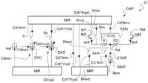
图1示出了示例性集成电路CI,该集成电路包括并入差分对晶体管NP、NM的放大器AMP。FIG. 1 shows an exemplary integrated circuit CI including an amplifier AMP incorporating a differential pair of transistors NP, NM.
具体实施方式Detailed ways
差分对的每个晶体管NP、NM由其栅极上的相应输入信号INP、INM控制。晶体管NP被定位于正输入端INP处,并且晶体管NM被定位于负输入端INM处。Each transistor NP, NM of the differential pair is controlled by a corresponding input signal INP, INM on its gate. Transistor NP is positioned at the positive input terminal INP, and transistor NM is positioned at the negative input terminal INM.
差分对晶体管NP、NM的源极经由相应电阻元件R1、R2连接到偏置节点Nd。相应电阻元件R1、R2具有相同的电阻值。The sources of the differential pair transistors NP, NM are connected to the bias node Nd via respective resistive elements R1, R2. The respective resistance elements R1, R2 have the same resistance value.
晶体管NP、NM的漏极各自形成差分对的相应输出。The drains of transistors NP, NM each form a respective output of a differential pair.
集成电路CI包括偏置电流生成器GIdiff,该偏置电流生成器被配置为生成被施加到偏置节点Nd的偏置电流2*Idiff。The integrated circuit CI includes a bias current generator GIdiff configured to generate a bias current 2*Idiff that is applied to the bias node Nd.
因此,以平衡的方式偏置晶体管NP、NM并且使每个通道具有相同的差分电流Idiff。晶体管漏极上的输出电压根据相应晶体管NP、NM的导通、根据输入信号INP、INM而变化。Therefore, transistors NP, NM are biased in a balanced manner and each channel has the same differential current Idiff. The output voltage on the drain of the transistor varies according to the conduction of the corresponding transistor NP, NM according to the input signal INP, INM.
为了使差分输出信号精确地表示输入信号之间的差异,对于差分对的两个晶体管NP、NM而言以相同的方式起作用是重要的。然而,在集成电路的生产期间,由于不可预测的物理偶然性,晶体管的特性(特别是阈值电压)可能会略有变化。In order for the differential output signal to accurately represent the difference between the input signals, it is important for the two transistors NP, NM of the differential pair to function in the same way. However, during the production of integrated circuits, the characteristics of transistors (especially threshold voltage) may vary slightly due to unpredictable physical contingencies.
集成电路CI包括补偿电流生成器GItrim,该补偿电流生成器被配置为生成补偿电流Cd*Itrim并将其引导到两个电阻元件R1、R2中的一个电阻元件中,以便补偿所述差分对晶体管NP、NM的的阈值电压的实际值之间的差异。The integrated circuit CI includes a compensation current generator GItrim configured to generate and direct a compensation current Cd*Itrim into one of the two resistive elements R1, R2 in order to compensate the differential pair transistors The difference between the actual values of the threshold voltages of NP and NM.
第一注入开关S1inj允许补偿电流注入支路Binj在正输入端INP的晶体管NP的源极侧连接到电阻元件R1。The first injection switch S1inj allows the compensation current injection branch Binj to be connected to the resistive element R1 at the source side of the transistor NP of the positive input INP.
第二注入开关S2inj允许补偿电流注入支路Binj在负输入端INM的晶体管NM的源极侧连接到电阻元件R2。The second injection switch S2inj allows the compensation current injection branch Binj to be connected to the resistive element R2 at the source side of the transistor NM of the negative input INM.
补偿电流提取支路Bext连接到电阻元件R1或R2中的一个或另一个电阻元件的另一端子,即,连接到偏置节点Nd。如果不需要补偿,则提取开关Sext允许将提取支路Next断开。The compensation current extraction branch Bext is connected to the other terminal of one or the other of the resistive elements R1 or R2, ie to the bias node Nd. The extraction switch Sext allows the extraction branch Next to be opened if compensation is not required.
补偿电流生成器GItrim被配置为将补偿电流Cd*Itrim注入到补偿电流注入支路Binj中,并从补偿电流提取支路Bext提取补偿电流Cd*Itrim。The compensation current generator GItrim is configured to inject the compensation current Cd*Itrim into the compensation current injection branch Binj and extract the compensation current Cd*Itrim from the compensation current extraction branch Bext.
因此,根据需要,形成了跨两个电阻元件R1、R2中的一个电阻元件端子的、用于引导补偿电流Cd*Itrim的路径,并且对补偿电流Cd*Itrim的引导对偏置电流2*Idiff的动态没有影响。Thus, as required, a path is formed across the terminals of one of the two resistive elements R1, R2 for conducting the compensation current Cd*Itrim, and the conduct of the compensation current Cd*Itrim to the bias current 2*Idiff dynamic has no effect.
此外,例如,如果正输入端INP的晶体管NP呈现出略低于负输入端INM的晶体管NM的阈值电压的阈值电压,则补偿电流Cd*Itrim经由闭合的第一注入开关S1inj以及闭合的提取开关Sext,被引导到耦合至晶体管NP的电阻元件R1中。Furthermore, for example, if the transistor NP of the positive input terminal INP exhibits a threshold voltage slightly lower than the threshold voltage of the transistor NM of the negative input terminal INM, the compensation current Cd*Itrim passes through the closed first injection switch S1inj and the closed extraction switch Sext, is directed into resistive element R1 coupled to transistor NP.
生成跨电阻器R1端子的电压Cd*Itrim*R1,并且将晶体管NP的源极电压增大相同的值。因此,正输入端INP上稍高的输入信号Cd*Itrim*R1将控制晶体管NP,正如其阈值电压稍高(即与预期值相比)一样。A voltage Cd*Itrim*R1 is generated across the terminals of resistor R1 and the source voltage of transistor NP is increased by the same value. Therefore, a slightly higher input signal Cd*Itrim*R1 on the positive input INP will control transistor NP as if its threshold voltage was slightly higher (ie compared to the expected value).
支配该均衡的等式如下:The equation governing this equilibrium is as follows:
INP–Vgsp–(Cd*Itrim+Idiff)*R=INM–Vgsm–Idiff*R;INP–Vgsp–(Cd*Itrim+Idiff)*R=INM–Vgsm–Idiff*R;
其中,INP和INM是相应输入的电压,Vgsp是晶体管NP的栅极-源极电压,Vgsm是晶体管NM的栅极-源极电压,Cd*Itrim是补偿电流,Idiff是差分电流,以及R是电阻元件R1、R2的电阻值;where INP and INM are the voltages of the corresponding inputs, Vgsp is the gate-source voltage of transistor NP, Vgsm is the gate-source voltage of transistor NM, Cd*Itrim is the compensation current, Idiff is the differential current, and R is the Resistance value of resistance elements R1, R2;
并且,对于相同的输入电压INP=INM,And, for the same input voltage INP=INM,
Vgsm=Vgsp+Cd*Itrim*R。Vgsm=Vgsp+Cd*Itrim*R.
其中,Cd是可以被控制的整数代码,并且Itrim是固定的基本补偿电流,为了补偿晶体管NP、NM的阈值电压之间的电位偏移,存在等于Itrim*R的电压增量。Where Cd is an integer code that can be controlled, and Itrim is a fixed basic compensation current, in order to compensate for the potential shift between the threshold voltages of transistors NP, NM, there is a voltage increment equal to Itrim*R.
因此,可以根据电阻值R来设定基本补偿电流Itrim强度的大小,以便具有更大或更小的大小的增量。Therefore, the magnitude of the strength of the basic compensation current Itrim can be set according to the resistance value R to have larger or smaller increments of magnitude.
例如,为了具有1mV的增量,在R=1kΩ时,会生成1μA的电流Itrim;或在R=100Ω时,会生成10μA的电流Itrim。代码Cd使得可以根据待被补偿的差分对晶体管NP、NM的阈值电压的实际值之间的差异,来将阈值电压的补偿校准为Cd*1mV。For example, to have a 1 mV increment, when R=1 kΩ, a current Itrim of 1 μA is generated; or when R=100Ω, a current Itrim of 10 μA is generated. The code Cd makes it possible to calibrate the compensation of the threshold voltage to Cd*1 mV according to the difference between the actual values of the threshold voltages of the differential pair transistors NP, NM to be compensated.
当然,电阻元件R1、R2的电阻值R可以与上文示例不同,并且增量Itrim*R也可以被选择为不同。Of course, the resistance values R of the resistive elements R1, R2 can be different from the above example, and the increment Itrim*R can also be chosen to be different.
在生产差分对晶体管NP、NM之前,选择基本电流Itrim的强度值和电阻值R。Before producing the differential pair transistors NP, NM, the strength value and the resistance value R of the basic current Itrim are chosen.
就代码Cd和待被闭合的注入开关而言,它们在以下阶段期间被选择:根据在生产时获得的晶体管NP、NM的阈值电压值之间的差异来表征集成电路生产时的组件。As far as the code Cd and the injection switch to be closed are concerned, they are selected during the phase of characterizing the components at the time of production of the integrated circuit according to the difference between the threshold voltage values of the transistors NP, NM obtained at the time of production.
在本文所描述的示例中,补偿电流生成器GIltrim包括可控的电流生成器DAC。例如,可控的电流生成器DAC能够接收数字命令Cdnum,该数字命令对基准电流Iref上的增益进行参数化,以使得以受控的强度递送补偿电流Cd*Itrim。In the example described herein, the compensation current generator GIltrim includes a controllable current generator DAC. For example, the controllable current generator DAC can receive a digital command Cdnum that parameterizes the gain on the reference current Iref such that the compensation current Cd*Itrim is delivered at a controlled intensity.
基准电流Iref由电流镜电路MIR和补偿电流生成器GItrim上游的基准电流生成器生成。The reference current Iref is generated by the current mirror circuit MIR and the reference current generator upstream of the compensation current generator GItrim.
电流镜电路MIR被配置为分别通过所述补偿电流注入支路和补偿电流提取支路Binj、Bext传输补偿电流Cd*Itrim。The current mirror circuit MIR is configured to transmit the compensation current Cd*Itrim through the compensation current injection branch and the compensation current extraction branch Binj, Bext, respectively.
电流镜电路MIR的作用是隔离寄生电容,该寄生电容可能由可控式电流生成器DAC引入到差分对晶体管NP、NM的电路中。The function of the current mirror circuit MIR is to isolate the parasitic capacitance, which may be introduced into the circuit of the differential pair transistors NP, NM by the controllable current generator DAC.
开关S连接在可控的电流生成器DAC的输出端处,以便在未配置补偿时将该电流生成器DAC与电流镜MIR断开。A switch S is connected at the output of the controllable current generator DAC to disconnect the current generator DAC from the current mirror MIR when compensation is not configured.
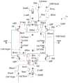
图2图示了示例性集成电路CI,该集成电路包括并入了差分对晶体管NP、NM的比较器设备CMP。FIG. 2 illustrates an exemplary integrated circuit CI including a comparator device CMP incorporating differential pair transistors NP, NM.
比较器CMP的电路包括参考图1所述的运算放大器AMP的电路。相同的元件带有相同的参考标记,并且此处将不再赘述。The circuit of the comparator CMP includes the circuit of the operational amplifier AMP described with reference to FIG. 1 . Identical elements bear the same reference numerals and will not be repeated here.
除了补偿电流生成器GIltim之外,比较器CMP进一步包括迟滞电流生成器GIhyst。In addition to the compensation current generator GIltim, the comparator CMP further includes a hysteresis current generator GIhyst.
迟滞电流生成器GIhyst被配置为在电阻元件R1中生成迟滞电流Cdh*Ihyst,该电阻元件根据差分输入端INP、INM的极性和根据差分对晶体管的n或p导电类型,耦合到处于稳定状态的晶体管NP的源极。The hysteresis current generator GIhyst is configured to generate a hysteresis current Cdh*Ihyst in the resistive element R1, which is coupled to be in steady state according to the polarities of the differential inputs INP, INM and according to the n or p conductivity type of the differential pair transistors the source of the transistor NP.
换言之,针对n型晶体管对的晶体管耦合到正输入端INP,并且针对p型晶体管对的晶体管耦合到负输入端INM。In other words, the transistors for the n-type transistor pair are coupled to the positive input INP, and the transistors for the p-type transistor pair are coupled to the negative input INM.
因此,迟滞电流Cdh*Ihyst将迟滞偏移引入到所述差分对晶体管NP、NM中的晶体管的阈值电压的实际值中。Hence, the hysteresis current Cdh*Ihyst introduces a hysteresis offset into the actual value of the threshold voltages of the transistors of the differential pair transistors NP, NM.
迟滞电流生成器GIhyst被配置为由迟滞命令Cmdh控制。通常从比较器CMP的输出端(未示出)发出迟滞命令,其表示比较的稳定状态。The hysteresis current generator GIhyst is configured to be controlled by the hysteresis command Cmdh. A hysteresis command is typically issued from the output of the comparator CMP (not shown), which represents the steady state of the comparison.
此外,以类似于补偿电流Cd*Itrim的注入-提取的方式,迟滞电流生成器GIhyst被配置为将迟滞电流注入支路Bhinj和迟滞电流提取支路Bhext电耦合到所述电阻元件R1的每个端子。Furthermore, in a manner similar to the injection-extraction of the compensation current Cd*Itrim, the hysteresis current generator GIhyst is configured to electrically couple the hysteresis current injection branch Bhinj and the hysteresis current extraction branch Bhext to each of said resistive elements R1 terminal.
迟滞命令Cmdh控制迟滞电流注入支路Bhinj上的开关Shinj以及迟滞电流提取支路Bhext上的开关Shext。The hysteresis command Cmdh controls the switch Shinj on the hysteresis current injection branch Bhinj and the switch Sheext on the hysteresis current extraction branch Bhext.
因此可以将迟滞电流Cdh*Ihyst注入到迟滞电流注入支路Bhinj中,并且从所述迟滞电流提取支路Bhext提取迟滞电流Cdh*Ihyst。It is thus possible to inject the hysteresis current Cdh*Ihyst into the hysteresis current injection branch Bhinj and extract the hysteresis current Cdh*Ihyst from the hysteresis current extraction branch Bhext.
以该方式,生成跨电阻元件R1的端子的等于Cdh*Ihyst*R1的迟滞偏移电压。In this way, a hysteretic offset voltage equal to Cdh*Ihyst*R1 is generated across the terminals of the resistive element R1.
如同生成补偿电流Cd*Itrim一样,迟滞电流生成器GIhyst包括可控的电流生成器DAC,该可控的电流生成器能够接收数字命令Cdnum,该数字命令对在电流镜电路MIR和迟滞电流生成器上游所生成的基准电流Iref的增益进行参数化,使得以期望的强度递送迟滞电流Cdh*Ihyst。As well as generating the compensation current Cd*Itrim, the hysteresis current generator GIhyst comprises a controllable current generator DAC capable of receiving a digital command Cdnum which is The gain of the upstream generated reference current Iref is parameterized such that the hysteresis current Cdh*Ihyst is delivered at the desired strength.
相应电流镜电路MIR也被配置为通过所述迟滞电流注入支路Bhinj、和迟滞电流提取支路Bhext来传输迟滞电流Cdh*Ihyst。The corresponding current mirror circuit MIR is also configured to deliver the hysteresis current Cdh*Ihyst through the hysteresis current injection branch Bhinj and the hysteresis current extraction branch Bhext.
开关Sh连接在可控的电流生成器DAC的输出端处,以便在不要求迟滞时将该电流生成器DAC与电流镜MIR断开。A switch Sh is connected at the output of the controllable current generator DAC to disconnect the current generator DAC from the current mirror MIR when hysteresis is not required.
其中,Cdh是可以被控制的整数代码,并且Ihyst是固定的基本迟滞电流,为了将迟滞引入差分对INP、INM的输入电压中,存在等于Ihyst*R的电压增量。where Cdh is an integer code that can be controlled, and Ihyst is a fixed base hysteresis current, in order to introduce hysteresis into the input voltage of the differential pair INP, INM, there is a voltage increment equal to Ihyst*R.
因此,也可以根据电阻值R来设定基本迟滞电流Ihyst强度的大小,以便具有更大或更小大小的增量,从而调节迟滞偏移。Therefore, the magnitude of the basic hysteresis current Ihyst intensity can also be set according to the resistance value R so as to have a larger or smaller magnitude increment, thereby adjusting the hysteresis offset.
例如,为了具有10mV的迟滞增量,在R=1kΩ时,生成10μA的电流Ihyst;或在R=100Ω时,生成100μA的电流Ihyst。因此,代码Cdh可以将迟滞电压参数化为Cdh*10mV。For example, to have a hysteresis increment of 10 mV, when R=1 kΩ, a current Ihyst of 10 μA is generated; or when R=100Ω, a current Ihyst of 100 μA is generated. Therefore, the code Cdh can parameterize the hysteresis voltage as Cdh*10mV.
例如,数字命令Cdhnum被包含在迟滞控制信号Cmdh中,以便能够对迟滞电压的值进行参数化以供使用。For example, the digital command Cdhnum is included in the hysteresis control signal Cmdh in order to be able to parameterize the value of the hysteresis voltage for use.
此外,生成基准电流Iref的基准电流生成器可以被配置为以例如在集成电路CI的设计期间或在使用集成电路期间可能根据命令而选择的强度,来生成基准电流Iref。Furthermore, the reference current generator that generates the reference current Iref may be configured to generate the reference current Iref at a strength that may be selected on command, eg during the design of the integrated circuit CI or during use of the integrated circuit.
假定补偿电流current Cd*Itrim和迟滞电流Cdh*Ihyst的生成各自引起了施加到基准电流Iref的增益,则选择基准电流Iref的强度使得可以特别地调整对迟滞电流强度进行控制的增量并且可以调整对补偿电流强度进行选择的增量。Given that the generation of the compensation current current Cd*Itrim and the hysteresis current Cdh*Ihyst each causes a gain applied to the reference current Iref, the strength of the reference current Iref is chosen such that the increments in which the hysteresis current strength is controlled can be specifically adjusted and can be adjusted The selected increment for the compensation current strength.
图3示出了以上参考图2所描述的示例性集成电路CI的比较器CMP,该比较器包括第二差分对晶体管PP、PM。FIG. 3 shows the comparator CMP of the exemplary integrated circuit CI described above with reference to FIG. 2 , the comparator including a second differential pair of transistors PP, PM.
以上参考图2所描述的第一差分对晶体管NP、NM呈现n型导电,而第二差分对晶体管PP、PM呈现p型导电。The first differential pair transistors NP, NM described above with reference to FIG. 2 exhibit n-type conduction, while the second differential pair transistors PP, PM exhibit p-type conduction.
在第二差分对PP、PM中,以与第一差分对NP、NM中的布局对称的形式来配置补偿电流生成器GIltrim。In the second differential pair PP, PM, the compensation current generator GIltrim is configured in a form symmetrical to the layout in the first differential pair NP, NM.
因此,补偿电流生成器GItrim包括补偿电流注入支路Binj和补偿电流提取支路Bext,该补偿电流注入支路和该补偿电流提取支路分别通过相应的开关S1ext、S2ext耦合到两个电阻元件R1、R2中的一个电阻元件的端子。将补偿电流Cd*Itrim注入到补偿电流注入支路Binj中,并从补偿电流提取支路Bext提取补偿电流Cd*Itrim。Therefore, the compensation current generator GItrim comprises a compensation current injection branch Binj and a compensation current extraction branch Bext, which are respectively coupled to the two resistive elements R1 through corresponding switches S1ext, S2ext , a terminal of a resistive element in R2. The compensation current Cd*Itrim is injected into the compensation current injection branch Binj, and the compensation current Cd*Itrim is extracted from the compensation current extraction branch Bext.
然而,在第二差分对PP、PM中,开关S1ext、S2ext被定位于补偿电流提取支路Bext上,这些开关将补偿电流注入-提取路径Binj、Bext与相应晶体管PP、PM的源极侧的两个电阻元件R1、R2中的一个或另一个电阻元件耦合。However, in the second differential pair PP, PM, switches S1ext, S2ext are positioned on the compensation current extraction branch Bext, which switches inject the compensation current into-extraction paths Binj, Bext with the source side of the respective transistors PP, PM One or the other of the two resistive elements R1, R2 is coupled.
补偿电流注入支路Binj也经由注入开关Sinj耦合到偏置节点Nd。The compensation current injection branch Binj is also coupled to the bias node Nd via the injection switch Sinj.
类似地,在第二差分对PP、PM中,以与第一差分对NP、NM中的布局对称的形式来配置迟滞电流生成器GIhyst。Similarly, in the second differential pair PP, PM, the hysteresis current generator GIhyst is configured in a form symmetrical to the layout in the first differential pair NP, NM.
因此,迟滞电流生成器GIhyst被配置为响应于迟滞控制信号Cmdh,通过相应的开关Shinj、Shext,将迟滞电流注入支路Bhinj和迟滞电流提取支路Bhext分别电耦合至所述电阻元件R1的每个端子。Therefore, the hysteresis current generator GIhyst is configured to, in response to the hysteresis control signal Cmdh, electrically couple the hysteresis current injection branch Bhinj and the hysteresis current extraction branch Bhext to each of the resistive elements R1 through the corresponding switches Shinj, Sheext, respectively. terminals.
因此,可以将迟滞电流Cdh*Ihyst注入到所述迟滞电流注入支路Bhinj中并且从所述迟滞电流提取支路Bhext提取迟滞电流Cdh*Ihyst。Therefore, the hysteresis current Cdh*Ihyst can be injected into the hysteresis current injection branch Bhinj and the hysteresis current Cdh*Ihyst can be extracted from the hysteresis current extraction branch Bhext.
如上所述,在耦合到处于稳定状态的晶体管PM(即,耦合到第二差分对晶体管的负输入端INM的晶体管,该晶体管的导电类型为p型)源极的电阻元件R2中生成迟滞电流Cdh*Ihyst。As described above, a hysteresis current is generated in the resistive element R2 coupled to the source of the transistor PM in steady state (ie, the transistor coupled to the negative input INM of the second differential pair transistor, which is of p-type conductivity) Cdh*Ihyst.
以上参考图2所描述的电流镜MIR可以被有利地共享以用于两个差分对的补偿电流和迟滞电流。The current mirror MIR described above with reference to Figure 2 can be advantageously shared for the compensation and hysteresis currents of the two differential pairs.
以上参考图1至3所描述的示例性集成电路CI有利地使得可以补偿差分对中的晶体管之间的阈值电压偏移,并且如果适用,可以将迟滞偏移引入比较器的输入端中。The exemplary integrated circuit CI described above with reference to FIGS. 1 to 3 advantageously makes it possible to compensate for threshold voltage shifts between transistors in a differential pair and, if applicable, to introduce hysteresis shifts into the inputs of the comparators.
在以上示例性集成电路中,晶体管的源极与偏置节点之间的电压最小,并且特别地由于连接到差分对的开关数目有限,所以寄生电容也最小。In the above exemplary integrated circuits, the voltage between the source and bias nodes of the transistors is minimal, and in particular the parasitic capacitance is minimal due to the limited number of switches connected to the differential pair.
此外,补偿和迟滞不取决于偏置电流,并且因此可以例如相对于温度变化以及以小增量的形式而被最优地配置,并且此外可以通过生成基准电流Iref而被调整。Furthermore, the compensation and hysteresis are not dependent on the bias current and can therefore be configured optimally, eg with respect to temperature changes and in small increments, and furthermore can be adjusted by generating the reference current Iref.
Claims (24)
Applications Claiming Priority (2)
| Application Number | Priority Date | Filing Date | Title |
|---|---|---|---|
| FR1906167AFR3097387B1 (en) | 2019-06-11 | 2019-06-11 | Method of biasing a differential pair of transistors, and corresponding integrated circuit |
| FR1906167 | 2019-06-11 |
Publications (2)
| Publication Number | Publication Date |
|---|---|
| CN112073042Atrue CN112073042A (en) | 2020-12-11 |
| CN112073042B CN112073042B (en) | 2025-09-23 |
Family
ID=68424990
Family Applications (2)
| Application Number | Title | Priority Date | Filing Date |
|---|---|---|---|
| CN202010499172.3AActiveCN112073042B (en) | 2019-06-11 | 2020-06-04 | Method for biasing differential pair transistors and corresponding integrated circuit |
| CN202021003317.8UActiveCN212258923U (en) | 2019-06-11 | 2020-06-04 | integrated circuit |
Family Applications After (1)
| Application Number | Title | Priority Date | Filing Date |
|---|---|---|---|
| CN202021003317.8UActiveCN212258923U (en) | 2019-06-11 | 2020-06-04 | integrated circuit |
Country Status (3)
| Country | Link |
|---|---|
| US (1) | US10985750B2 (en) |
| CN (2) | CN112073042B (en) |
| FR (1) | FR3097387B1 (en) |
Families Citing this family (1)
| Publication number | Priority date | Publication date | Assignee | Title |
|---|---|---|---|---|
| FR3097387B1 (en)* | 2019-06-11 | 2021-05-28 | St Microelectronics Rousset | Method of biasing a differential pair of transistors, and corresponding integrated circuit |
Citations (7)
| Publication number | Priority date | Publication date | Assignee | Title |
|---|---|---|---|---|
| JPH03173289A (en)* | 1989-12-01 | 1991-07-26 | Toshiba Corp | Maximum/minimum circuit |
| CN1611004A (en)* | 2001-12-28 | 2005-04-27 | 皇家飞利浦电子股份有限公司 | Regenerating amplifier circuit |
| CN1957527A (en)* | 2004-03-31 | 2007-05-02 | 模拟设备股份有限公司 | Differential stage voltage offset trimming circuit |
| CN102136827A (en)* | 2011-05-10 | 2011-07-27 | 覃超 | Differential amplifier capable of compensating input offset voltage and compensating method |
| DE202014002367U1 (en)* | 2014-03-17 | 2014-04-15 | Dialog Semiconductor Gmbh | Dynamic hysteresis comparator |
| US20190108886A1 (en)* | 2017-10-11 | 2019-04-11 | Stmicroelectronics S.R.L. | Reading Circuit and Method for a Non-Volatile Memory Device |
| CN212258923U (en)* | 2019-06-11 | 2020-12-29 | 意法半导体(鲁塞)公司 | integrated circuit |
Family Cites Families (8)
| Publication number | Priority date | Publication date | Assignee | Title |
|---|---|---|---|---|
| JPS5591219A (en)* | 1978-12-28 | 1980-07-10 | Nippon Gakki Seizo Kk | Amplifier |
| JP4058334B2 (en)* | 2002-12-12 | 2008-03-05 | 旭化成エレクトロニクス株式会社 | Hysteresis comparator circuit |
| TWI226751B (en)* | 2003-09-02 | 2005-01-11 | Prolific Technology Inc | Hysteresis circuits used in comparator |
| JP4628881B2 (en)* | 2005-06-15 | 2011-02-09 | ルネサスエレクトロニクス株式会社 | Variable gain amplifier circuit, DC offset correction method thereof, and wireless receiver |
| US7292083B1 (en)* | 2006-04-18 | 2007-11-06 | Etron Technology, Inc. | Comparator circuit with Schmitt trigger hysteresis character |
| JP4956460B2 (en)* | 2008-02-14 | 2012-06-20 | 株式会社リコー | Voltage comparison circuit, semiconductor integrated circuit having the voltage comparison circuit, and electronic device |
| US7973569B1 (en)* | 2010-03-17 | 2011-07-05 | Microchip Technology Incorporated | Offset calibration and precision hysteresis for a rail-rail comparator with large dynamic range |
| FR3083654B1 (en)* | 2018-07-05 | 2021-04-02 | St Microelectronics Rousset | POLARIZATION METHOD OF THE OUTPUTS OF A FOLDED CASCODE STAGE OF A COMPARATOR AND CORRESPONDING COMPARATOR |
- 2019
- 2019-06-11FRFR1906167Apatent/FR3097387B1/enactiveActive
- 2020
- 2020-05-28USUS16/885,737patent/US10985750B2/enactiveActive
- 2020-06-04CNCN202010499172.3Apatent/CN112073042B/enactiveActive
- 2020-06-04CNCN202021003317.8Upatent/CN212258923U/enactiveActive
Patent Citations (7)
| Publication number | Priority date | Publication date | Assignee | Title |
|---|---|---|---|---|
| JPH03173289A (en)* | 1989-12-01 | 1991-07-26 | Toshiba Corp | Maximum/minimum circuit |
| CN1611004A (en)* | 2001-12-28 | 2005-04-27 | 皇家飞利浦电子股份有限公司 | Regenerating amplifier circuit |
| CN1957527A (en)* | 2004-03-31 | 2007-05-02 | 模拟设备股份有限公司 | Differential stage voltage offset trimming circuit |
| CN102136827A (en)* | 2011-05-10 | 2011-07-27 | 覃超 | Differential amplifier capable of compensating input offset voltage and compensating method |
| DE202014002367U1 (en)* | 2014-03-17 | 2014-04-15 | Dialog Semiconductor Gmbh | Dynamic hysteresis comparator |
| US20190108886A1 (en)* | 2017-10-11 | 2019-04-11 | Stmicroelectronics S.R.L. | Reading Circuit and Method for a Non-Volatile Memory Device |
| CN212258923U (en)* | 2019-06-11 | 2020-12-29 | 意法半导体(鲁塞)公司 | integrated circuit |
Also Published As
| Publication number | Publication date |
|---|---|
| US10985750B2 (en) | 2021-04-20 |
| FR3097387B1 (en) | 2021-05-28 |
| US20200395932A1 (en) | 2020-12-17 |
| FR3097387A1 (en) | 2020-12-18 |
| CN112073042B (en) | 2025-09-23 |
| CN212258923U (en) | 2020-12-29 |
Similar Documents
| Publication | Publication Date | Title |
|---|---|---|
| US5726597A (en) | Method and circuit for reducing offset voltages for a differential input stage | |
| KR101742343B1 (en) | Driving method for obtaining a gain linear variation of a transconductance amplifier and corresponding driving circuit | |
| US7902894B2 (en) | Accurate hysteretic comparator and method | |
| US6998917B2 (en) | Common-mode feedback circuit and differential operational amplifier circuit having stable operation and low power consumption | |
| KR20180034555A (en) | Complementary current field effect transistor device and amplifier | |
| US10630274B2 (en) | Method for biasing outputs of a folded cascode stage in a comparator and corresponding comparator | |
| TW200935752A (en) | Current steering DAC and voltage booster for current steering DAC | |
| TW201329668A (en) | Circuit for a current having a programmable temperature slope | |
| JP2017519426A (en) | Feed forward bias circuit | |
| CN212258923U (en) | integrated circuit | |
| US8723593B2 (en) | Bias voltage generation circuit and differential circuit | |
| US10754369B2 (en) | Reference current source and semiconductor device | |
| US9432015B2 (en) | Hysteresis comparator circuit having differential input transistors with switched bulk bias voltages | |
| JPH08274550A (en) | Mos-technique current mirror including cascode stage with wide driving range | |
| US11031917B2 (en) | Method for generating a bias current for biasing a differential pair of transistors and corresponding integrated circuit | |
| KR101352410B1 (en) | Method for nullifying temperature dependence and circuit therefor | |
| JP3158000B2 (en) | Bias circuit | |
| KR100863529B1 (en) | Operational amplifier circuit | |
| JPH10112614A (en) | Bias current supply method and circuit thereof | |
| KR100554441B1 (en) | Current bias circuit of cascode current mirror | |
| JP4029958B2 (en) | Semiconductor circuit | |
| US10571946B2 (en) | Constant voltage output circuit | |
| KR101102970B1 (en) | Regulator Amplifiers and Regulator Circuits | |
| US8653859B2 (en) | Electronic comparison circuit | |
| JP2025125449A (en) | Differential amplifier, offset adjustment device, and method for adjusting input offset voltage of differential amplifier using the same |
Legal Events
| Date | Code | Title | Description |
|---|---|---|---|
| PB01 | Publication | ||
| PB01 | Publication | ||
| SE01 | Entry into force of request for substantive examination | ||
| SE01 | Entry into force of request for substantive examination | ||
| GR01 | Patent grant | ||
| GR01 | Patent grant |