CN112071760A - Semiconductor device and manufacturing method thereof - Google Patents
Semiconductor device and manufacturing method thereofDownload PDFInfo
- Publication number
- CN112071760A CN112071760ACN202011111165.8ACN202011111165ACN112071760ACN 112071760 ACN112071760 ACN 112071760ACN 202011111165 ACN202011111165 ACN 202011111165ACN 112071760 ACN112071760 ACN 112071760A
- Authority
- CN
- China
- Prior art keywords
- layer
- thermal annealing
- semiconductor device
- gallium oxide
- magnesium
- Prior art date
- Legal status (The legal status is an assumption and is not a legal conclusion. Google has not performed a legal analysis and makes no representation as to the accuracy of the status listed.)
- Granted
Links
- 239000004065semiconductorSubstances0.000titleclaimsabstractdescription27
- 238000004519manufacturing processMethods0.000titleclaimsabstractdescription14
- 238000000137annealingMethods0.000claimsabstractdescription41
- AJNVQOSZGJRYEI-UHFFFAOYSA-Ndigallium;oxygen(2-)Chemical compound[O-2].[O-2].[O-2].[Ga+3].[Ga+3]AJNVQOSZGJRYEI-UHFFFAOYSA-N0.000claimsabstractdescription28
- 229910001195gallium oxideInorganic materials0.000claimsabstractdescription28
- FYYHWMGAXLPEAU-UHFFFAOYSA-NMagnesiumChemical compound[Mg]FYYHWMGAXLPEAU-UHFFFAOYSA-N0.000claimsabstractdescription24
- 229910052749magnesiumInorganic materials0.000claimsabstractdescription24
- 239000011777magnesiumSubstances0.000claimsabstractdescription24
- RTAQQCXQSZGOHL-UHFFFAOYSA-NTitaniumChemical compound[Ti]RTAQQCXQSZGOHL-UHFFFAOYSA-N0.000claimsabstractdescription23
- 229910052719titaniumInorganic materials0.000claimsabstractdescription23
- 239000010936titaniumSubstances0.000claimsabstractdescription23
- PCHJSUWPFVWCPO-UHFFFAOYSA-NgoldChemical compound[Au]PCHJSUWPFVWCPO-UHFFFAOYSA-N0.000claimsabstractdescription18
- 239000010931goldSubstances0.000claimsabstractdescription18
- 229910052737goldInorganic materials0.000claimsabstractdescription18
- 239000000956alloySubstances0.000claimsdescription22
- 229910045601alloyInorganic materials0.000claimsdescription22
- 238000000034methodMethods0.000claimsdescription19
- 239000007789gasSubstances0.000claimsdescription16
- 239000001257hydrogenSubstances0.000claimsdescription12
- 229910052739hydrogenInorganic materials0.000claimsdescription12
- 238000000151depositionMethods0.000claimsdescription10
- UFHFLCQGNIYNRP-UHFFFAOYSA-NHydrogenChemical compound[H][H]UFHFLCQGNIYNRP-UHFFFAOYSA-N0.000claimsdescription8
- IJGRMHOSHXDMSA-UHFFFAOYSA-NAtomic nitrogenChemical compoundN#NIJGRMHOSHXDMSA-UHFFFAOYSA-N0.000claimsdescription7
- GYHNNYVSQQEPJS-UHFFFAOYSA-NGalliumChemical compound[Ga]GYHNNYVSQQEPJS-UHFFFAOYSA-N0.000claimsdescription6
- 229910052733galliumInorganic materials0.000claimsdescription6
- 150000002431hydrogenChemical class0.000claimsdescription4
- 229910052757nitrogenInorganic materials0.000claimsdescription4
- 239000010410layerSubstances0.000description74
- 238000005516engineering processMethods0.000description16
- 229910052751metalInorganic materials0.000description6
- 239000002184metalSubstances0.000description6
- QVGXLLKOCUKJST-UHFFFAOYSA-Natomic oxygenChemical compound[O]QVGXLLKOCUKJST-UHFFFAOYSA-N0.000description5
- 239000001301oxygenSubstances0.000description5
- 229910052760oxygenInorganic materials0.000description5
- 230000015572biosynthetic processEffects0.000description4
- 230000014509gene expressionEffects0.000description3
- 238000012986modificationMethods0.000description3
- 230000004048modificationEffects0.000description3
- 230000008569processEffects0.000description3
- 238000009792diffusion processMethods0.000description2
- 239000000463materialSubstances0.000description2
- 230000003647oxidationEffects0.000description2
- 238000007254oxidation reactionMethods0.000description2
- 230000005641tunnelingEffects0.000description2
- 230000008859changeEffects0.000description1
- 239000013078crystalSubstances0.000description1
- 230000007547defectEffects0.000description1
- 230000008021depositionEffects0.000description1
- 230000000694effectsEffects0.000description1
- 230000005669field effectEffects0.000description1
- 238000010438heat treatmentMethods0.000description1
- 238000001755magnetron sputter depositionMethods0.000description1
- 230000007246mechanismEffects0.000description1
- 238000001451molecular beam epitaxyMethods0.000description1
- QJGQUHMNIGDVPM-UHFFFAOYSA-Nnitrogen groupChemical group[N]QJGQUHMNIGDVPM-UHFFFAOYSA-N0.000description1
- 239000011241protective layerSubstances0.000description1
- 239000000523sampleSubstances0.000description1
Images


Classifications
- H—ELECTRICITY
- H01—ELECTRIC ELEMENTS
- H01L—SEMICONDUCTOR DEVICES NOT COVERED BY CLASS H10
- H01L21/00—Processes or apparatus adapted for the manufacture or treatment of semiconductor or solid state devices or of parts thereof
- H01L21/02—Manufacture or treatment of semiconductor devices or of parts thereof
- H01L21/04—Manufacture or treatment of semiconductor devices or of parts thereof the devices having potential barriers, e.g. a PN junction, depletion layer or carrier concentration layer
- H01L21/34—Manufacture or treatment of semiconductor devices or of parts thereof the devices having potential barriers, e.g. a PN junction, depletion layer or carrier concentration layer the devices having semiconductor bodies not provided for in groups H01L21/18, H10D48/04 and H10D48/07, with or without impurities, e.g. doping materials
- H01L21/44—Manufacture of electrodes on semiconductor bodies using processes or apparatus not provided for in groups H01L21/38 - H01L21/428
- H01L21/441—Deposition of conductive or insulating materials for electrodes
- H01L21/443—Deposition of conductive or insulating materials for electrodes from a gas or vapour, e.g. condensation
- H—ELECTRICITY
- H10—SEMICONDUCTOR DEVICES; ELECTRIC SOLID-STATE DEVICES NOT OTHERWISE PROVIDED FOR
- H10D—INORGANIC ELECTRIC SEMICONDUCTOR DEVICES
- H10D64/00—Electrodes of devices having potential barriers
- H10D64/60—Electrodes characterised by their materials
- H10D64/62—Electrodes ohmically coupled to a semiconductor
Landscapes
- Engineering & Computer Science (AREA)
- Physics & Mathematics (AREA)
- Condensed Matter Physics & Semiconductors (AREA)
- General Physics & Mathematics (AREA)
- Manufacturing & Machinery (AREA)
- Computer Hardware Design (AREA)
- Microelectronics & Electronic Packaging (AREA)
- Power Engineering (AREA)
- Electrodes Of Semiconductors (AREA)
Abstract
Translated fromChinese
Description
Translated fromChinese技术领域technical field
本发明涉及半导体器件制造领域,具体涉及一种半导体器件及其制造方法。The invention relates to the field of semiconductor device manufacturing, in particular to a semiconductor device and a manufacturing method thereof.
背景技术Background technique
在现今的半导体发展过程中,接触是十分关键的一步,影响着整个器件的性能,以及器件的功耗。其中欧姆接触一直是半导体工艺方面的一个难点。欧姆接触是指:一是半导体和金属接触时不产生明显的附加阻抗;二是不会使半导体内部的平衡载流子浓度发生显著变化。In today's semiconductor development process, contact is a very critical step, affecting the performance of the entire device, as well as the power consumption of the device. Among them, ohmic contact has always been a difficulty in semiconductor technology. Ohmic contact refers to: firstly, there is no obvious additional impedance when the semiconductor and metal contact; secondly, the equilibrium carrier concentration inside the semiconductor will not change significantly.
从理论上来说,影响金属与半导体形成欧姆接触的主要因素有两个:一是金属、半导体的功函数;二是半导体的表面态密度。目前制备氧化镓欧姆接触电极的方法主要利用的是隧穿机制。其将与金属电极接触的氧化镓材料近表面局部区域进行重掺杂,提高电子浓度,金属与半导体接触后,利用电子的隧穿效应,实现欧姆接触特性。相比之下,其工艺较为复杂,且重掺杂后对材料晶体质量的损伤严重。CN108461404A公开了一种利用镁层和金层组成合金层实现欧姆接触的方法,其通过单次热处理形成,但是其接触电阻较大,氧化镓内的氧空位较多,还是不能满足晶体管器件的高性能的要求。Theoretically, there are two main factors that affect the formation of ohmic contact between metal and semiconductor: one is the work function of the metal and the semiconductor; the other is the surface state density of the semiconductor. The current method for preparing gallium oxide ohmic contact electrodes mainly utilizes the tunneling mechanism. It heavily doped the local area near the surface of the gallium oxide material in contact with the metal electrode to increase the electron concentration. After the metal is in contact with the semiconductor, the tunneling effect of electrons is used to achieve ohmic contact characteristics. In contrast, the process is more complicated, and the crystal quality of the material is seriously damaged after heavy doping. CN108461404A discloses a method for realizing ohmic contact by using magnesium layer and gold layer to form an alloy layer, which is formed by a single heat treatment, but its contact resistance is relatively large, and there are many oxygen vacancies in gallium oxide, which still cannot meet the high requirements of transistor devices. performance requirements.
发明内容SUMMARY OF THE INVENTION
基于解决上述问题,本发明提供了一种半导体器件的制造方法,其包括以下步骤:Based on solving the above problems, the present invention provides a method for manufacturing a semiconductor device, which includes the following steps:
(1)提供一晶体管器件,所述晶体管器件具有顶部的氧化镓层;(1) providing a transistor device having a gallium oxide layer on top;
(2)在所述氧化镓层上沉积钛层,所述钛层的厚度为10-100nm;(2) depositing a titanium layer on the gallium oxide layer, and the thickness of the titanium layer is 10-100 nm;
(3)进行第一次热退火,所述第一次热退火的压强为0.5-1.2atm;(3) carrying out the first thermal annealing, and the pressure of the first thermal annealing is 0.5-1.2 atm;
(4)在所述钛层上沉积镁层,所述镁层的厚度为1-5μm;(4) depositing a magnesium layer on the titanium layer, and the thickness of the magnesium layer is 1-5 μm;
(5)在所述镁层上沉积金层,所述金层的厚度为0.5-2μm;(5) depositing a gold layer on the magnesium layer, and the thickness of the gold layer is 0.5-2 μm;
(6)进行第二次退火,所述第二次热退火的压强为0.01-0.1atm。(6) A second annealing is performed, and the pressure of the second thermal annealing is 0.01-0.1 atm.
根据本发明的实施例,其中,所述第一次热退火的温度为100-250℃,第二次热退火的温度为300-500℃。According to an embodiment of the present invention, the temperature of the first thermal annealing is 100-250°C, and the temperature of the second thermal annealing is 300-500°C.
根据本发明的实施例,其中,所述第一次热退火的时间为1-5min,所述第二次退火的时间为5-10min。According to an embodiment of the present invention, the time of the first thermal annealing is 1-5 min, and the time of the second annealing is 5-10 min.
根据本发明的实施例,所述第一次热退火和第二次热退火的气氛相同,均为氮气和氢气的混合气体,其中氢气占所述混合气体的体积比为5%。According to an embodiment of the present invention, the atmospheres of the first thermal annealing and the second thermal annealing are the same, and both are a mixed gas of nitrogen and hydrogen, wherein the volume ratio of hydrogen to the mixed gas is 5%.
本发明还提供了一种半导体器件封装件,其由上述的半导体器件封装件的制造方法形成,其包括:The present invention also provides a semiconductor device package, which is formed by the above-mentioned manufacturing method of a semiconductor device package, comprising:
氧化镓层Gallium oxide layer
第一合金层,位于所述氧化镓层上,所述第一合金层包括钛、镓和镁;a first alloy layer on the gallium oxide layer, the first alloy layer comprising titanium, gallium and magnesium;
第二合金层,位于所述第一合金层上,所述第二合金层包括镁和金。A second alloy layer is located on the first alloy layer, and the second alloy layer includes magnesium and gold.
根据本发明的实施例,所述第一合金层的厚度为0.1-0.5μm。According to an embodiment of the present invention, the thickness of the first alloy layer is 0.1-0.5 μm.
根据本发明的实施例,所述第二合金层的厚度为1-5μm。According to an embodiment of the present invention, the thickness of the second alloy layer is 1-5 μm.
本发明的优点如下:The advantages of the present invention are as follows:
利用钛层来保护氧化镓层,防止金层向氧化镓层的扩散;The titanium layer is used to protect the gallium oxide layer and prevent the diffusion of the gold layer to the gallium oxide layer;
第一次热退火时,还原性气氛可以钝化氧化镓层中的氧空位,同时钛层保护氧化镓的表面形态;During the first thermal annealing, the reducing atmosphere can passivate the oxygen vacancies in the gallium oxide layer, while the titanium layer protects the surface morphology of the gallium oxide;
第二次热退火的气压小于所述第二热退火的气压,还原性气氛钝化氧化镓中的氧空位且防止镁层和金层的氧化,同时使得各层中的气隙溢出,实现较好的欧姆接触。The gas pressure of the second thermal annealing is lower than the gas pressure of the second thermal annealing, and the reducing atmosphere passivates the oxygen vacancies in the gallium oxide and prevents the oxidation of the magnesium layer and the gold layer, and at the same time causes the air gaps in each layer to overflow, so as to achieve relatively Good ohmic contact.
附图说明Description of drawings
图1-4为半导体器件的制造方法流程示意图。1-4 are schematic flowcharts of a manufacturing method of a semiconductor device.
具体实施方式Detailed ways
本技术将通过参考实施例中的附图进行描述,本技术涉及一种半导体器件及其制造方法,该半导体器件的制造方法包括依次在氧化镓层上形成钛层、镁层和金层,并在形成钛层之后进行第一次热退火,在形成金层之后进行第二次热退火,其中,第一次热退火的气压大于所述第二次热退火的气压,以此来形成与氧化镓的欧姆接触。The present technology will be described with reference to the accompanying drawings in the embodiments, and the present technology relates to a semiconductor device and a method for fabricating the same, the method for fabricating the semiconductor device includes sequentially forming a titanium layer, a magnesium layer and a gold layer on a gallium oxide layer, and The first thermal annealing is performed after the titanium layer is formed, and the second thermal annealing is performed after the gold layer is formed, wherein the gas pressure of the first thermal annealing is greater than the gas pressure of the second thermal annealing, so as to form and oxidize Ohmic contact of gallium.
可以理解的是,本技术可以以许多不同的形式实现,并且不应被解释为限于在此阐述的实施例。当然,提供这些实施例,为的是使本公开彻底且全面,并且将该技术充分地传达给本领域技术人员。的确,该技术旨在涵盖这些实施例的替代、修改和等同物,其包含在由所附权利要求所限定的技术的范围和精神内。此外,在本技术的以下具体描述中,大量特定的细节被提出,以便提供对本技术彻底的理解。但是,对本领域技术人员显而易见的是,本技术在没有这些特定的细节时是可以实现的。It will be appreciated that the present technology may be implemented in many different forms and should not be construed as limited to the embodiments set forth herein. Rather, these embodiments are provided so that this disclosure will be thorough and complete, and will fully convey the technology to those skilled in the art. Indeed, this technology is intended to cover alternatives, modifications, and equivalents of these embodiments, which are included within the scope and spirit of the technology as defined by the appended claims. Furthermore, in the following detailed description of the present technology, numerous specific details are set forth in order to provide a thorough understanding of the present technology. However, it will be apparent to those skilled in the art that the present technology may be practiced without these specific details.
本文所用的术语“顶部的”和“底部的”,上部的”和“下部的”以及“垂直的”和“水平的”和它们的各种形式,只作示例和说明的目的,并不意味着限定本技术的描述,因为提及的项目可以在位置和方向上交换。并且,这里所用的术语“大体上”和/或“大约”的意思是,指定的尺寸或参数在给定应用的可接受制造公差内是可以变化的。The terms "top" and "bottom", "upper" and "lower" and "vertical" and "horizontal" and their various forms are used herein for purposes of illustration and description only and do not imply that is intended to limit the description of the present technology, as the items mentioned may be interchanged in position and orientation. Also, the terms "substantially" and/or "approximately" as used herein mean that the specified dimensions or parameters are Variations are possible within acceptable manufacturing tolerances.
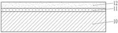
首先参考图1,氧化镓层10可以形成于晶体管器件的顶层上,其中,晶体管可以是肖特基二极管、HEMT、场效应晶体管等。该氧化镓层10可以通过任何已知的方法形成,例如磁控溅射、激光脉冲沉积、分子束外延生长等,其厚度可以是例如1-5μm。Referring first to FIG. 1, a
接着,在所述氧化镓层10上沉积一钛层11,所述钛层11的沉积方法可以与氧化镓10的形成方法相同。相对于后续形成的镁层和金层,钛层具有较薄的厚度,优选为10-100nm。Next, a
然后进行第一次热退火处理,所述第一次热退火处理的条件为:温度为100-250℃,时间为1-5min,气压为0.5-1.2atm,气氛为氮气和氢气的混合气体,其中氢气占所述混合气体的体积比为5%。在第一次热退火处理中,其气压较大,可以大于1atm,以此使得混合气体中的氢气可以进入氧化镓中,以钝化氧化镓中的氧空位。该氢气可以是D2或H2。而较薄的钛层11则在第一次热退火时充当保护层,保证可氧化镓表面的致密性。Then the first thermal annealing treatment is performed, and the conditions of the first thermal annealing treatment are: the temperature is 100-250° C., the time is 1-5 min, the pressure is 0.5-1.2 atm, and the atmosphere is a mixed gas of nitrogen and hydrogen, The volume ratio of hydrogen in the mixed gas is 5%. In the first thermal annealing treatment, the gas pressure is relatively high, which can be greater than 1 atm, so that the hydrogen in the mixed gas can enter the gallium oxide to passivate the oxygen vacancies in the gallium oxide. Thehydrogen can be D2 orH2 . The
参见图2,在所述钛层11上沉积镁层12,所述镁层12的厚度远大于所述钛层11,优选为1-5μm。所述镁层12的沉积方法可以与氧化镓10和钛层11的形成方法相同。Referring to FIG. 2 , a
参见图3,在所述镁层12上沉积金层13,所述金层13的厚度略小于所述镁层12,优选为0.5-2μm。所述金层13的沉积方法可以与氧化镓10、钛层11和镁层12的形成方法相同,以此来简化工艺步骤。Referring to FIG. 3 , a
接着,参见图4,进行第二次热退火处理,所述第二次热退火处理的条件为:温度为300-500℃,时间为5-10min,气压为0.01-0.1atm,气氛为氮气和氢气的混合气体,其中氢气占所述混合气体的体积比为5%。在第二次热退火处理中,其气压相较于第一次热退火较小,以此使得各层中的气隙溢出,保证各层缺陷较少。氢气可以进一步钝化氧化镓中的氧空位,并可以防止各金属层被氧化。该氢气同样可以是D2或H2。Next, referring to FIG. 4 , a second thermal annealing treatment is performed. The conditions of the second thermal annealing treatment are: the temperature is 300-500° C., the time is 5-10 min, the gas pressure is 0.01-0.1 atm, and the atmosphere is nitrogen and A mixed gas of hydrogen, wherein the volume ratio of hydrogen to the mixed gas is 5%. In the second thermal annealing treatment, the gas pressure is lower than that in the first thermal annealing, so that the air gaps in each layer overflow, ensuring fewer defects in each layer. Hydrogen can further passivate the oxygen vacancies in the gallium oxide and can prevent oxidation of the various metal layers. The hydrogen can likewise be D2 or H2 .
在进行第二热退火处理之后,钛层11融入镁层12中形成第一合金层14,所述第二合金层14的厚度稍薄,可以是0.1-0.5μm。在第一合金层14中还包括少量的镓,其通过热扩散进入所述第一合金层14。而镁层12的大部分则与其上的金层13熔合形成第二合金层15,第二合金层15的厚度稍大,其可以是1-5μm,其中,该第二合金层15包括镁和镓。After the second thermal annealing process, the
利用四探针法测得的上述欧姆接触的方块电阻均小于100Ω/sq,相较于最后直接进行单次气氛热退火,具有较小的欧姆接触电阻。The sheet resistances of the above ohmic contacts measured by the four-point probe method are all less than 100Ω/sq, and have lower ohmic contact resistances compared to the single-pass atmospheric thermal annealing at the end.
为了说明和描述的目的,本技术的前面的详细描述已经呈现。其并不旨在将本技术详尽或限制于所公开的精确形式。根据上述教导的许多修改和变化是可以的。选择所描述的实施例是为了最好地解释本技术的原理及其实际应用,从而确保其他本领域的技术人员最好地利用各种实施例中的技术和适用于预期的特定用途的各种修改。本技术的范围由所附的权利要求限定。The foregoing detailed description of the present technology has been presented for the purposes of illustration and description. It is not intended to be exhaustive or to limit the technology to the precise form disclosed. Many modifications and variations are possible in light of the above teachings. The described embodiments were chosen in order to best explain the principles of the present technology and its practical application, to thereby ensure others skilled in the art to best utilize the technology in the various embodiments and with the various implementations as are suited to the particular use contemplated. Revise. The scope of the present technology is defined by the appended claims.
本发明中使用的表述“示例性实施例”、“示例”等不是指同一实施例,而是被提供来着重描述不同的特定特征。然而,上述示例和示例性实施例不排除他们与其他示例的特征相组合来实现。例如,即使在另一示例中未提供特定示例的描述的情况下,除非另有陈述或与其他示例中的描述相反,否则该描述可被理解为与另一示例相关的解释。The expressions "exemplary embodiment," "exemplary," etc. used in this disclosure do not refer to the same embodiment, but are instead provided to highlight different specific features. However, the above-described examples and exemplary embodiments do not exclude their realization in combination with features of other examples. For example, even if a description of a particular example is not provided in another example, the description may be construed as an explanation in relation to the other example unless otherwise stated or contrary to the description in the other example.
本发明中使用的术语仅用于示出示例,而无意限制本发明。除非上下文中另外清楚地指明,否则单数表述包括复数表述。The terms used in the present invention are only used to illustrate examples, and are not intended to limit the present invention. Singular expressions include plural expressions unless the context clearly indicates otherwise.
虽然以上示出并描述了示例实施例,但对本领域技术人员将明显的是,在不脱离由权利要求限定的本发明的范围的情况下,可做出变型和改变。While example embodiments have been shown and described above, it will be apparent to those skilled in the art that modifications and changes can be made without departing from the scope of the invention as defined by the claims.
Claims (7)
Translated fromChinesePriority Applications (1)
| Application Number | Priority Date | Filing Date | Title |
|---|---|---|---|
| CN202011111165.8ACN112071760B (en) | 2020-10-16 | 2020-10-16 | A kind of semiconductor device and its manufacturing method |
Applications Claiming Priority (1)
| Application Number | Priority Date | Filing Date | Title |
|---|---|---|---|
| CN202011111165.8ACN112071760B (en) | 2020-10-16 | 2020-10-16 | A kind of semiconductor device and its manufacturing method |
Publications (2)
| Publication Number | Publication Date |
|---|---|
| CN112071760Atrue CN112071760A (en) | 2020-12-11 |
| CN112071760B CN112071760B (en) | 2022-10-28 |
Family
ID=73656017
Family Applications (1)
| Application Number | Title | Priority Date | Filing Date |
|---|---|---|---|
| CN202011111165.8AActiveCN112071760B (en) | 2020-10-16 | 2020-10-16 | A kind of semiconductor device and its manufacturing method |
Country Status (1)
| Country | Link |
|---|---|
| CN (1) | CN112071760B (en) |
Citations (7)
| Publication number | Priority date | Publication date | Assignee | Title |
|---|---|---|---|---|
| US5963829A (en)* | 1995-03-15 | 1999-10-05 | Nec Corporation | Method of forming silicide film |
| US20130056793A1 (en)* | 2011-09-07 | 2013-03-07 | Applied Materials, Inc. | Providing group v and group vi over pressure for thermal treatment of compound semiconductor thin films |
| CN107993934A (en)* | 2017-12-08 | 2018-05-04 | 中国科学院微电子研究所 | Method for enhancing ohmic contact of gallium oxide semiconductor device |
| CN108400115A (en)* | 2017-02-04 | 2018-08-14 | 中芯国际集成电路制造(上海)有限公司 | A kind of semiconductor devices and its manufacturing method and electronic device |
| CN108461404A (en)* | 2018-05-23 | 2018-08-28 | 大连理工大学 | A kind of preparation method of gallium oxide Ohm contact electrode |
| CN109671612A (en)* | 2018-11-15 | 2019-04-23 | 中国科学院上海微系统与信息技术研究所 | A kind of gallium oxide semiconductor structure and preparation method thereof |
| CN111128873A (en)* | 2019-12-30 | 2020-05-08 | 广州粤芯半导体技术有限公司 | Wafer surface metal alloying treatment method |
- 2020
- 2020-10-16CNCN202011111165.8Apatent/CN112071760B/enactiveActive
Patent Citations (7)
| Publication number | Priority date | Publication date | Assignee | Title |
|---|---|---|---|---|
| US5963829A (en)* | 1995-03-15 | 1999-10-05 | Nec Corporation | Method of forming silicide film |
| US20130056793A1 (en)* | 2011-09-07 | 2013-03-07 | Applied Materials, Inc. | Providing group v and group vi over pressure for thermal treatment of compound semiconductor thin films |
| CN108400115A (en)* | 2017-02-04 | 2018-08-14 | 中芯国际集成电路制造(上海)有限公司 | A kind of semiconductor devices and its manufacturing method and electronic device |
| CN107993934A (en)* | 2017-12-08 | 2018-05-04 | 中国科学院微电子研究所 | Method for enhancing ohmic contact of gallium oxide semiconductor device |
| CN108461404A (en)* | 2018-05-23 | 2018-08-28 | 大连理工大学 | A kind of preparation method of gallium oxide Ohm contact electrode |
| CN109671612A (en)* | 2018-11-15 | 2019-04-23 | 中国科学院上海微系统与信息技术研究所 | A kind of gallium oxide semiconductor structure and preparation method thereof |
| CN111128873A (en)* | 2019-12-30 | 2020-05-08 | 广州粤芯半导体技术有限公司 | Wafer surface metal alloying treatment method |
Also Published As
| Publication number | Publication date |
|---|---|
| CN112071760B (en) | 2022-10-28 |
Similar Documents
| Publication | Publication Date | Title |
|---|---|---|
| CN102687247B (en) | N-type contact electrode of group III nitride semiconductor and method for forming the same | |
| CN111063742B (en) | Gallium oxide-based PN junction structure and preparation method thereof | |
| CN101276872B (en) | Method for forming electrode for group iii nitride compound semiconductor light-emitting device | |
| CN101303978A (en) | Manufacturing method suitable for N-type ohmic contact of gallium nitride device | |
| JP2008270836A (en) | Semiconductor device | |
| JP2005033212A (en) | Thin film electrode for high performance gallium nitride based light emitting device and method of manufacturing the same | |
| WO2019154222A1 (en) | Ohmic contact structure of nitride semiconductor device and manufacturing method therefor | |
| CN107578989B (en) | Method for manufacturing N-type SiC ohmic contact electrode | |
| CN101567383A (en) | Ohmic electrode structure for silicon carbide and manufacturing method thereof | |
| CN102414848B (en) | Semiconductor element and process for producing semiconductor element | |
| TWI225709B (en) | A semiconductor device and method for fabricating the same | |
| CN112071760A (en) | Semiconductor device and manufacturing method thereof | |
| CN108364864A (en) | The preparation method of AlGaN/GaN HEMT device Ohm contact electrodes | |
| RU2619444C1 (en) | METHOD FOR PRODUCING OHMIC CONTACTS TO NITRIDE HETEROSTRUCTURES ON Si/Al BASIS | |
| JP2004247709A (en) | Semiconductor device and manufacturing method thereof | |
| CN102254936B (en) | Compound semiconductor device and method for manufacturing compound semiconductor device | |
| JPWO2017169364A1 (en) | N-type electrode, method for manufacturing n-type electrode, and n-type laminated structure including n-type electrode on n-type group III nitride single crystal layer | |
| CN110164989A (en) | N-type AlxGa1-xAs material system semiconductor surface Ohm contact electrode and preparation method thereof | |
| JP3654037B2 (en) | Ohmic electrode, manufacturing method thereof, and semiconductor device | |
| CN116344601A (en) | A method for manufacturing ohmic contacts of gallium nitride devices | |
| CN115863405A (en) | A kind of ohmic contact structure and its preparation method, HEMT device | |
| CN206947351U (en) | N-type GaN polarization doping Ohm contact electrodes | |
| CN115732538A (en) | A kind of semiconductor device and its manufacturing method | |
| JP4283502B2 (en) | Group 3-5 compound semiconductor electrode, method for producing the same, and semiconductor light emitting device using the same | |
| CN117558750B (en) | SiC/Al/Ti ohmic contact electrode of p-type 4H-SiC, preparation method thereof and semiconductor device comprising electrode |
Legal Events
| Date | Code | Title | Description |
|---|---|---|---|
| PB01 | Publication | ||
| PB01 | Publication | ||
| SE01 | Entry into force of request for substantive examination | ||
| SE01 | Entry into force of request for substantive examination | ||
| TA01 | Transfer of patent application right | ||
| TA01 | Transfer of patent application right | Effective date of registration:20220928 Address after:518054 A801, Zhongdi Building, University of Geosciences, No. 8, Yuexing Third Road, Yuehai Street, Nanshan District, Shenzhen, Guangdong Applicant after:SHENZHEN TEAMMAX TECHNOLOGY CO.,LTD. Address before:1506, Huiyuan Building, 38 Huaneng Road, Lixia District, Jinan City, Shandong Province Applicant before:SHANDONG AOTIAN ENVIRONMENTAL PROTECTION TECHNOLOGY CO.,LTD. | |
| GR01 | Patent grant | ||
| GR01 | Patent grant |