CN112050097A - Luminous line group - Google Patents
Luminous line groupDownload PDFInfo
- Publication number
- CN112050097A CN112050097ACN201910604259.XACN201910604259ACN112050097ACN 112050097 ACN112050097 ACN 112050097ACN 201910604259 ACN201910604259 ACN 201910604259ACN 112050097 ACN112050097 ACN 112050097A
- Authority
- CN
- China
- Prior art keywords
- light
- emitting
- packaged
- light guide
- guiding
- Prior art date
- Legal status (The legal status is an assumption and is not a legal conclusion. Google has not performed a legal analysis and makes no representation as to the accuracy of the status listed.)
- Pending
Links
Images


Classifications
- F—MECHANICAL ENGINEERING; LIGHTING; HEATING; WEAPONS; BLASTING
- F21—LIGHTING
- F21S—NON-PORTABLE LIGHTING DEVICES; SYSTEMS THEREOF; VEHICLE LIGHTING DEVICES SPECIALLY ADAPTED FOR VEHICLE EXTERIORS
- F21S2/00—Systems of lighting devices, not provided for in main groups F21S4/00 - F21S10/00 or F21S19/00, e.g. of modular construction
- G—PHYSICS
- G02—OPTICS
- G02B—OPTICAL ELEMENTS, SYSTEMS OR APPARATUS
- G02B6/00—Light guides; Structural details of arrangements comprising light guides and other optical elements, e.g. couplings
- G02B6/24—Coupling light guides
- G02B6/42—Coupling light guides with opto-electronic elements
- G02B6/4201—Packages, e.g. shape, construction, internal or external details
- G02B6/4202—Packages, e.g. shape, construction, internal or external details for coupling an active element with fibres without intermediate optical elements, e.g. fibres with plane ends, fibres with shaped ends, bundles
- G02B6/4203—Optical features
- G—PHYSICS
- G02—OPTICS
- G02B—OPTICAL ELEMENTS, SYSTEMS OR APPARATUS
- G02B6/00—Light guides; Structural details of arrangements comprising light guides and other optical elements, e.g. couplings
- G02B6/10—Light guides; Structural details of arrangements comprising light guides and other optical elements, e.g. couplings of the optical waveguide type
- G02B6/12—Light guides; Structural details of arrangements comprising light guides and other optical elements, e.g. couplings of the optical waveguide type of the integrated circuit kind
- G02B6/12004—Combinations of two or more optical elements
- F—MECHANICAL ENGINEERING; LIGHTING; HEATING; WEAPONS; BLASTING
- F21—LIGHTING
- F21V—FUNCTIONAL FEATURES OR DETAILS OF LIGHTING DEVICES OR SYSTEMS THEREOF; STRUCTURAL COMBINATIONS OF LIGHTING DEVICES WITH OTHER ARTICLES, NOT OTHERWISE PROVIDED FOR
- F21V19/00—Fastening of light sources or lamp holders
- F21V19/001—Fastening of light sources or lamp holders the light sources being semiconductors devices, e.g. LEDs
- G—PHYSICS
- G02—OPTICS
- G02B—OPTICAL ELEMENTS, SYSTEMS OR APPARATUS
- G02B6/00—Light guides; Structural details of arrangements comprising light guides and other optical elements, e.g. couplings
- G02B6/0001—Light guides; Structural details of arrangements comprising light guides and other optical elements, e.g. couplings specially adapted for lighting devices or systems
- G02B6/0011—Light guides; Structural details of arrangements comprising light guides and other optical elements, e.g. couplings specially adapted for lighting devices or systems the light guides being planar or of plate-like form
- G02B6/0066—Light guides; Structural details of arrangements comprising light guides and other optical elements, e.g. couplings specially adapted for lighting devices or systems the light guides being planar or of plate-like form characterised by the light source being coupled to the light guide
- G02B6/0068—Arrangements of plural sources, e.g. multi-colour light sources
- G—PHYSICS
- G02—OPTICS
- G02B—OPTICAL ELEMENTS, SYSTEMS OR APPARATUS
- G02B6/00—Light guides; Structural details of arrangements comprising light guides and other optical elements, e.g. couplings
- G02B6/0001—Light guides; Structural details of arrangements comprising light guides and other optical elements, e.g. couplings specially adapted for lighting devices or systems
- G02B6/0011—Light guides; Structural details of arrangements comprising light guides and other optical elements, e.g. couplings specially adapted for lighting devices or systems the light guides being planar or of plate-like form
- G02B6/0081—Mechanical or electrical aspects of the light guide and light source in the lighting device peculiar to the adaptation to planar light guides, e.g. concerning packaging
- G02B6/0083—Details of electrical connections of light sources to drivers, circuit boards, or the like
- G—PHYSICS
- G02—OPTICS
- G02B—OPTICAL ELEMENTS, SYSTEMS OR APPARATUS
- G02B6/00—Light guides; Structural details of arrangements comprising light guides and other optical elements, e.g. couplings
- G02B6/24—Coupling light guides
- G02B6/42—Coupling light guides with opto-electronic elements
- G02B6/4201—Packages, e.g. shape, construction, internal or external details
- G02B6/4204—Packages, e.g. shape, construction, internal or external details the coupling comprising intermediate optical elements, e.g. lenses, holograms
- G02B6/4214—Packages, e.g. shape, construction, internal or external details the coupling comprising intermediate optical elements, e.g. lenses, holograms the intermediate optical element having redirecting reflective means, e.g. mirrors, prisms for deflecting the radiation from horizontal to down- or upward direction toward a device
- G—PHYSICS
- G02—OPTICS
- G02B—OPTICAL ELEMENTS, SYSTEMS OR APPARATUS
- G02B6/00—Light guides; Structural details of arrangements comprising light guides and other optical elements, e.g. couplings
- G02B6/24—Coupling light guides
- G02B6/42—Coupling light guides with opto-electronic elements
- G02B6/4201—Packages, e.g. shape, construction, internal or external details
- G02B6/4274—Electrical aspects
- G02B6/428—Electrical aspects containing printed circuit boards [PCB]
- G—PHYSICS
- G06—COMPUTING OR CALCULATING; COUNTING
- G06F—ELECTRIC DIGITAL DATA PROCESSING
- G06F1/00—Details not covered by groups G06F3/00 - G06F13/00 and G06F21/00
- G06F1/16—Constructional details or arrangements
- G06F1/18—Packaging or power distribution
- G06F1/183—Internal mounting support structures, e.g. for printed circuit boards, internal connecting means
- H—ELECTRICITY
- H04—ELECTRIC COMMUNICATION TECHNIQUE
- H04B—TRANSMISSION
- H04B10/00—Transmission systems employing electromagnetic waves other than radio-waves, e.g. infrared, visible or ultraviolet light, or employing corpuscular radiation, e.g. quantum communication
- H04B10/80—Optical aspects relating to the use of optical transmission for specific applications, not provided for in groups H04B10/03 - H04B10/70, e.g. optical power feeding or optical transmission through water
- H04B10/806—Arrangements for feeding power
- H04B10/808—Electrical power feeding of an optical transmission system
- F—MECHANICAL ENGINEERING; LIGHTING; HEATING; WEAPONS; BLASTING
- F21—LIGHTING
- F21V—FUNCTIONAL FEATURES OR DETAILS OF LIGHTING DEVICES OR SYSTEMS THEREOF; STRUCTURAL COMBINATIONS OF LIGHTING DEVICES WITH OTHER ARTICLES, NOT OTHERWISE PROVIDED FOR
- F21V2200/00—Use of light guides, e.g. fibre optic devices, in lighting devices or systems
- F21V2200/10—Use of light guides, e.g. fibre optic devices, in lighting devices or systems of light guides of the optical fibres type
- F—MECHANICAL ENGINEERING; LIGHTING; HEATING; WEAPONS; BLASTING
- F21—LIGHTING
- F21Y—INDEXING SCHEME ASSOCIATED WITH SUBCLASSES F21K, F21L, F21S and F21V, RELATING TO THE FORM OR THE KIND OF THE LIGHT SOURCES OR OF THE COLOUR OF THE LIGHT EMITTED
- F21Y2115/00—Light-generating elements of semiconductor light sources
- F21Y2115/10—Light-emitting diodes [LED]
- G—PHYSICS
- G02—OPTICS
- G02B—OPTICAL ELEMENTS, SYSTEMS OR APPARATUS
- G02B6/00—Light guides; Structural details of arrangements comprising light guides and other optical elements, e.g. couplings
- G02B6/24—Coupling light guides
- G02B6/42—Coupling light guides with opto-electronic elements
- G02B6/4201—Packages, e.g. shape, construction, internal or external details
- G02B6/4249—Packages, e.g. shape, construction, internal or external details comprising arrays of active devices and fibres
- G—PHYSICS
- G02—OPTICS
- G02B—OPTICAL ELEMENTS, SYSTEMS OR APPARATUS
- G02B6/00—Light guides; Structural details of arrangements comprising light guides and other optical elements, e.g. couplings
- G02B6/24—Coupling light guides
- G02B6/42—Coupling light guides with opto-electronic elements
- G02B6/4201—Packages, e.g. shape, construction, internal or external details
- G02B6/4274—Electrical aspects
- G02B6/4283—Electrical aspects with electrical insulation means
Landscapes
- Physics & Mathematics (AREA)
- Engineering & Computer Science (AREA)
- General Physics & Mathematics (AREA)
- Optics & Photonics (AREA)
- General Engineering & Computer Science (AREA)
- Theoretical Computer Science (AREA)
- Microelectronics & Electronic Packaging (AREA)
- Human Computer Interaction (AREA)
- Power Engineering (AREA)
- Computer Hardware Design (AREA)
- Electromagnetism (AREA)
- Computer Networks & Wireless Communication (AREA)
- Signal Processing (AREA)
- Planar Illumination Modules (AREA)
- Optical Couplings Of Light Guides (AREA)
Abstract
Translated fromChinese
Description
Translated fromChinese技术领域technical field
本发明是有关于一种排线,特别是有关于一种发光线组。The present invention relates to a flat cable, in particular to a light-emitting cable group.
背景技术Background technique
近年来,电竞(e-sport)产业发展迅速,因此也带动了电竞产业所使用的软件与硬件设备的发展。关于硬件设备,除了追求更快的运算处理速度以外,硬件设备的造型也不断地创新,希望创造出更能吸引消费者目光的产品。In recent years, the e-sports industry has developed rapidly, which has also driven the development of software and hardware equipment used in the e-sports industry. Regarding hardware devices, in addition to pursuing faster computing processing speed, the shape of hardware devices is also constantly innovating, hoping to create products that are more attractive to consumers.
为了成功吸引消费者的目光,许多电竞相关产品结合发光元件,制作成具有发光效果的设备,例如常用于电竞活动的鼠标、键盘、机壳、主机板等。In order to successfully attract the attention of consumers, many e-sports-related products are combined with light-emitting components to make devices with luminous effects, such as mice, keyboards, casings, and motherboards that are commonly used in e-sports activities.
在结合电竞设备与发光元件时,电竞设备内的电子元件与发光元件之间的排列方式,将会影响到最终组装后的设备尺寸大小。在不增加设备体积以及不缩减内部包含的元件尺寸的前提下,较佳的内部元件排列方式,有助于在固定的体积内容纳更多元件,例如容纳更多发光元件,使得该电竞设备的发光方式更多变。When combining gaming equipment and light-emitting elements, the arrangement of the electronic components and light-emitting elements in the gaming equipment will affect the size of the final assembled equipment. On the premise of not increasing the volume of the device and reducing the size of the components contained in the device, a better arrangement of internal components helps to accommodate more components in a fixed volume, such as accommodating more light-emitting components, so that the gaming device can be The way it shines is more variable.
发明内容SUMMARY OF THE INVENTION
本发明提供一种发光线组,包括至少两导光缆线彼此相邻,其中各该导光缆线各自包含有一导电材以及一导光材,其中该导光材包覆该导电材,以及多个封装发光元件,其中每一条导光缆线对应该多个封装发光元件中的至少一封装发光元件,且该些封装发光元件位于各该导光缆线的一末段,其中该封装发光元件的一最小边长大于该导光材的一厚度,且从一剖面方向来看,一连心线连接该两导光缆线各自的一中心,且该多个封装发光元件中的至少一个封装发光元件与该连心线的一中垂线重叠。The present invention provides a light-emitting wire set, comprising at least two light guide cables adjacent to each other, wherein each of the light guide cables includes a conductive material and a light guide material, wherein the light guide material covers the conductive material, and a plurality of Packaged light-emitting elements, wherein each light-guiding cable corresponds to at least one packaged light-emitting element in the plurality of packaged light-emitting elements, and the packaged light-emitting elements are located at an end of each of the light-guiding cables, wherein a minimum of the packaged light-emitting elements The side length is greater than a thickness of the light guide material, and viewed from a cross-sectional direction, a central line connects a center of each of the two light guide cables, and at least one of the plurality of packaged light-emitting elements is connected to the connection. A mid-perpendicular line of the heart line overlaps.
本发明的特征在于,当每一条导光缆线的周围设置更多的封装发光元件,代表更强的光源可以照射至导光缆线的导光材内,增加软性发光线材的显示光效强度,且同时也提高光传导的距离。但是当导光缆线周围设置的封装发光元件数量增加时,也同时需要更多的空间去容纳该些导光缆线以及封装发光元件。因此本发明以改变封装发光元件的排列方式,不需要缩减各元件的尺寸,也不需要增加导光材的厚度,即可使得导光缆线之间排列得更紧密,进而节省空间。The present invention is characterized in that, when more encapsulated light-emitting elements are arranged around each light-guiding cable, it means that a stronger light source can be irradiated into the light-guiding material of the light-guiding cable, thereby increasing the display light effect intensity of the flexible light-emitting wire. At the same time, the distance of light transmission is also increased. However, when the number of packaged light-emitting elements disposed around the light-guiding cables increases, more space is also required to accommodate the light-guiding cables and the packaged light-emitting elements. Therefore, the present invention changes the arrangement of the packaged light-emitting elements without reducing the size of each element or increasing the thickness of the light-guiding material, so that the light-guiding cables can be arranged more closely, thereby saving space.
附图说明Description of drawings
图1绘示根据本发明一较佳实施例的软性发光线组俯视图。FIG. 1 is a top view of a flexible light-emitting wire group according to a preferred embodiment of the present invention.
图2为沿着图1的剖面线A-A’所得的剖面图。Fig. 2 is a cross-sectional view taken along the section line A-A' of Fig. 1 .
图3则为软性发光线组的局部立体示意图。FIG. 3 is a partial three-dimensional schematic diagram of the flexible light-emitting line group.
图4绘示本发明另一较佳实施例的软性发光线组的剖面图。FIG. 4 is a cross-sectional view of a flexible light-emitting wire group according to another preferred embodiment of the present invention.
图4A绘示本发明包含二次光学系统的软性发光线组的一实施例示意图。FIG. 4A is a schematic diagram of an embodiment of the flexible light-emitting line group including the secondary optical system of the present invention.
图4B绘示本发明包含二次光学系统的软性发光线组的一实施例示意图。FIG. 4B is a schematic diagram of an embodiment of the flexible light-emitting line group including the secondary optical system of the present invention.
图4C绘示本发明包含二次光学系统的软性发光线组的一实施例示意图。FIG. 4C is a schematic diagram of an embodiment of the flexible light-emitting line group including the secondary optical system of the present invention.
图4D绘示本发明包含二次光学系统的软性发光线组的一实施例示意图。FIG. 4D is a schematic diagram of an embodiment of the flexible light-emitting line group including the secondary optical system of the present invention.
图5绘示沿着图3的剖面线B-B’所得的剖面图。FIG. 5 is a cross-sectional view taken along the section line B-B' of FIG. 3 .
图6绘示根据本发明另一较佳实施例的封装发光元件的排列方式。FIG. 6 illustrates an arrangement of packaged light-emitting elements according to another preferred embodiment of the present invention.
图7绘示根据本发明另一较佳实施例的封装发光元件的排列方式。FIG. 7 illustrates an arrangement of packaged light-emitting elements according to another preferred embodiment of the present invention.
图8绘示根据本发明另一较佳实施例的封装发光元件的排列方式。FIG. 8 illustrates the arrangement of the packaged light-emitting elements according to another preferred embodiment of the present invention.
图9绘示根据本发明另一较佳实施例的封装发光元件的排列方式。FIG. 9 illustrates an arrangement of packaged light-emitting elements according to another preferred embodiment of the present invention.
图10绘示根据本发明另一较佳实施例的封装发光元件的排列方式。FIG. 10 illustrates the arrangement of the packaged light-emitting elements according to another preferred embodiment of the present invention.
附图标号reference number
10 导光缆线10 Light guide cable
11 导电材11 Conductive material
12 导光材12 Light guide material
20 封装发光元件20 Packaged light-emitting elements
22 印刷电路板22 printed circuit board
24 通孔24 through hole
26 发光单元26 light units
26A 红色发光单元26A red light unit
26B 绿色发光单元26B green light-emitting unit
26C 蓝色发光单元26C blue light-emitting unit
30 控制器30 Controllers
31 壳体31 Housing
50 连接器50 connector
60 二次光学系统60 Secondary Optical System
60A 二次光学系统60A Secondary Optical System
60B 二次光学系统60B Secondary Optical System
60C 二次光学系统60C Secondary Optical System
60D 二次光学系统60D Secondary Optical System
100 软性发光线组100 Soft Glowing Cord Sets
312 上半部312 top half
314 下半部314 Lower half
315 侧边315 Side
316 侧边316 Side
C1 中心C1 Center
C2 中心C2 Center
G1 间隙宽度G1 gap width
G2 间隙宽度G2 gap width
H1 通孔H1 through hole
H2 通孔H2 through hole
L 光线L light
L1 连心线L1 connecting wire
P 突出部P protrusion
P1 突出部P1 protrusion
P2 突出部P2 protrusion
P3 突出部P3 protrusion
t 厚度t Thickness
T 中垂线T mid-perpendicular
S 图案S pattern
具体实施方式Detailed ways
为使本领域相关技术人员能更进一步了解本发明,下文特列举本发明的较佳实施例,并配合所附图式,详细说明本发明的构成内容及所欲达成的功效。In order to enable those skilled in the art to further understand the present invention, the preferred embodiments of the present invention are listed below, and the components of the present invention and the desired effects are described in detail in conjunction with the accompanying drawings.
为了方便说明,本发明的各图式仅为示意以更容易了解本发明,其详细的比例可依照设计的需求进行调整。在文中所描述对于图形中相对元件的上下关系,在本领域的人皆应能理解其系指物件的相对位置而言,因此皆可以翻转而呈现相同的构件,此皆应同属本说明书所揭露的范围,在此容先叙明。For the convenience of description, the drawings of the present invention are merely schematic to facilitate understanding of the present invention, and the detailed proportions thereof can be adjusted according to design requirements. The up-down relationship of the relative elements in the drawings described in the text should be understood by those in the art to refer to the relative positions of the objects, so they can all be turned over to present the same components, which should all belong to the disclosure of this specification. range, which is described here first.
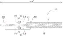
请参阅图1、图2及图3,其绘示根据本发明一较佳实施例的软性发光线组。图1绘示根据本发明一较佳实施例的软性发光线组俯视图;图2为沿着图1的剖面线A-A’所得的剖面图;图3则为软性发光线组100的局部立体示意图。本发明的软性发光线组100至少包括多条导光缆线,举例来说,本实施例中有六条相互平行的导光缆线10。各导光缆线10皆各自包括一导电材11以及一导光材12,其中导光材12包覆于导电材11外侧。在本实施例中,上述导光缆线10具有相同的尺寸,更进一步而言,各导光缆线的导电材11的直径也彼此相同,且各导光材12的厚度也都相等,因此每一条导光缆线10均具有相同的直径,但本发明不限于此。在其他实施例中,也可以因应实际需求而制作出不同直径的导光缆线,也属于本发明的涵盖范围内。Please refer to FIG. 1 , FIG. 2 and FIG. 3 , which illustrate a flexible light-emitting wire group according to a preferred embodiment of the present invention. 1 is a top view of a flexible light-emitting wire group according to a preferred embodiment of the present invention; FIG. 2 is a cross-sectional view taken along the section line AA' of FIG. 1 ; Partial perspective view. The flexible light-emitting wire set 100 of the present invention at least includes a plurality of light guide cables, for example, there are six
值得注意的是,本实施例中虽然画出一共六条导光缆线10,但本发明不限于此。本发明的软性发光线组100可能包含有更多或是更少条导光缆线,仅须满足具有两条以上的导光缆线,均可属于本发明的涵盖范围内。It should be noted that although a total of six
在本实施例中,导电材11作为软性发光线组100用来连接电信号的导电轴心,材质例如为软铜线、镀银软铜线等。而导光材12覆盖于导电材外侧,主要为透明或半透明材质,例如聚碳酸酯树脂、玻璃或其他合适的材料。其中至少一导电材11电连接一电源,例如为电脑设备中的电源供应器。In this embodiment, the
此外,在导光材12的内部,除了导电材11之外,还可以包含有信号线(图未示),用来传输信号。因此本发明的软性发光线组100除了当作电源线使用之外,也可以当作信号传输线使用,或两者的组合。In addition, in the inside of the
请参考图2与图3,本实施例中,更包含有多个封装发光元件20,每一个封装发光元件例如封装完成的发光二极管(LED),内部包含有多个LED(发光单元)以及部分导电线路。其中,每一条导光缆线10都对应至少一个以上的封装发光元件20。举例来说,本实施例中每一条导光缆线10都各自对应四个封装发光元件20,位于各导光缆线10的一端,且每四个封装发光元件20围绕在各导光缆线10的周围,尤其是围绕在各导光缆线10的导电材11周围。Please refer to FIG. 2 and FIG. 3 , in this embodiment, a plurality of packaged light-emitting
本实施例中,每一个封装发光元件20皆位于一印刷电路板22上,其中印刷电路板22包含有多个通孔24,各通孔24较佳平行排列,且对应各导光缆线10的导电材11的位置,而封装发光元件被安装于印刷电路板22上的通孔24周围。因此,在本实施例的结构中,各导光缆线10的导电材11皆穿过该些通孔24,形成各封装发光元件20围绕各导光缆线10的导电材11的结构。此外,各导光缆线10的一轴心方向与图3所示的Y方向平行,而印刷电路板22的平面方向则与图3所示的X-Z平面平行,也就是说,印刷电路板22与各导光缆线10的延伸方向互相垂直。In this embodiment, each packaged light-emitting
此外,虽然在本实施例中,仅设置有单一个印刷电路板22,且所有的封装发光元件20均安装于印刷电路板22上,但本发明不限于此,在其他实施例中,也可能包含有多个印刷电路板22。In addition, although in this embodiment, only a single printed
值得注意的是,各封装发光元件20上都包含有多个发光单元26,各该发光单元例如为一发光二极管或是一激光二极管,较佳而言,每一个封装发光元件20上都包含有可发出三种不同颜色光源的发光单元,例如红色发光二极管(Light-emitting diode,LED)、绿色发光二极管与蓝色发光二极管,或者是红色激光二极管(Laser diode)、绿色激光二极管与蓝色激光二极管。上述红光、绿光与蓝光分别为光的三原色,因此可以组合成各种颜色的光源。It should be noted that each packaged light-emitting
在本发明的其他实施例中,每一个封装发光元件20所包含的发光单元26的颜色或数量可以调整。举例来说,在一些实施例中,封装发光元件20包含有单色光源(例如为红、蓝、绿三者其中之一的光源或其他颜色的光源),或是双色光源(例如红、蓝、绿三者其中之二,或是其两种任意不同颜色的光源),或是四种或四种以上不同颜色的光源,以上实施例皆属于本发明的涵盖范围内。In other embodiments of the present invention, the color or number of the light-emitting
在本实施例中,如图2所示,各封装发光元件20的发光单元26皆可发出光线L,且光线L照向各导光缆线10的导光材12,导光材12可以传导光线(也就是来自发光单元26所发出的光线L),使得软性发光线组100具有均匀发光的效果。导光材12可以为电性绝缘材料,除了导光之外,也可以兼做导电材11及/或信号线的绝缘包覆材料。在另一实施例中,导电材11的外部可以先包覆一层绝缘材料,例如聚乙烯或聚氯乙烯,然后在绝缘材料的外部再包覆上述导光层12。其中上述绝缘材料较佳为白色或是浅色材质,以增加光线在导光材12中传输时的反射或折射效果。In this embodiment, as shown in FIG. 2 , the light-emitting
此外,更包含有一控制器30,连接各封装发光元件20,以控制封装发光元件20上的各发光单元26,例如开启/关闭光源、调整光线的强弱、或是通过开启部分颜色的光源而组合成新的颜色的光源,例如同时开启红光与蓝光可组合成紫光等,其中控制器30可电连接于至少一导光缆线10的导电材11,使电源供电于控制器30及各该封装发光元件20。In addition, a
控制器30包括一壳体31,在本实施例中,壳体31包括上半部312及下半部314,上半部312与下半部314可经由螺栓或卡扣等结构锁固组合而形成壳体31,而且壳体31中形成一容纳空间,可容纳印刷电路板22,另外,壳体31的两相对侧边315与侧边316形成多个通孔H1及通孔H2,该等导光缆线10经由该等通孔H1穿入该壳体31,并且通过壳体31的上半部312及下半部314夹持固定。The
本发明的软性发光线组100更包括一连接器50,连接器50例如为电脑设备中所用的接头或连接端口,常见的有6针(6-PIN)连接端口或24针(24-PIN)连接端口等,适用于连接电脑的电源供应器、主机板或显示卡等硬件设备,但不限于此。该等导光缆线10的导电材11结合于连接器50,更进一步说,该等导光缆线10的导电材11是连接于连接器50的端子,在本实施例中,该等导光缆线10的两端分别各连接于一连接器50。The flexible light-emitting wire set 100 of the present invention further includes a
在本发明的另一实施例中,为了更有效地引导光线进入导光材中,可以在封装发光元件以及导光材之间,设置额外设置一个二次光学系统。图4绘示本发明另一较佳实施例的软性发光线组的剖面图。请一并参考图4与上述图2,在图4所示的实施例中,在封装发光元件20以及导光材12之间设置一个二次光学系统60,此二次光学系统60内部可能包含有多个反射镜、多个折射镜或是其组合。设置二次光学系统60的目的在于集中发光单元26所发出的光线L,增加进入导光材12的入光量,进而提高软性发光线组的发光强度与光线传导的距离。In another embodiment of the present invention, in order to guide light into the light guide material more effectively, an additional secondary optical system may be disposed between the packaged light-emitting element and the light guide material. FIG. 4 is a cross-sectional view of a flexible light-emitting wire group according to another preferred embodiment of the present invention. Please refer to FIG. 4 and the above-mentioned FIG. 2 together. In the embodiment shown in FIG. 4 , a secondary
图4A至图4D绘示本发明不同种类的二次光学系统的示意图。请参考图4A所示的二次光学系统60A,本实施例中的二次光学系统60A可改变光线前进方向,利用折射方式将光线导入导光材12中;请参考图4B所示的二次光学系统60B,本实施例中的二次光学系统60B可改变光线前进方向,利用反射方式将光线导入导光材12中;请参考图4C所示的二次光学系统60C,本实施例中的二次光学系统60C可改变光线前进方向,利用全反射方式将光线导入导光材12中;或是请参考图4D所示的二次光学系统60D,本实施例中的二次光学系统60D可改变光线前进方向,利用导光方式将光线导入导光材12中。值得注意的是,上述各实施例的二次光学系统也可以相互组合,且本实施例所述的二次光学系统可以与本发明所述的其他任何实施例结合。以下段落仍以第一实施例(图1至图3)为例进行说明。4A to 4D are schematic diagrams illustrating different types of secondary optical systems of the present invention. Please refer to the secondary
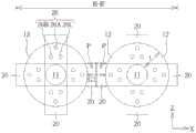
图5绘示沿着图3的剖面线B-B’所得的剖面图。为了简化图式,图5主要绘出部分导光缆线10以及部分封装发光元件20的排列位置,而其余的元件将省略于图上。在本实施例中,从一剖面方向来看(也就是从图3的XZ平面方向),各封装发光元件20围绕于导光缆线10的周围。在本发明中,为了提高软性发光线组100的发光强度与发光长度,可以增加设置在各导光缆线10周围的封装发光元件20的数量。换句话说,当每一条导光缆线10的周围设置更多的封装发光元件20,代表更强的光源可以照射至导光缆线10的导光材12内,增加软性发光线材100显示光效强度,且同时也提高光传导的距离。在本实施例中,每一条导光缆线10周围设置四个封装发光元件20,但不以此为限,每一条导光缆线可对应的封装发光元件数量可依照实际需求而调整。FIG. 5 is a cross-sectional view taken along the section line B-B' of FIG. 3 . In order to simplify the drawing, FIG. 5 mainly depicts the arrangement positions of part of the
如图5所示,在本实施例中每一个封装发光元件20排列于导光缆线10的导电材11的四个方位,例如沿着X轴与Z轴,排列于导光缆线10的导电材11的正上方、正下方、正左方与正右方。值得注意的是,从剖面图(图5)来看,各封装发光元件20并不接触导电材11,以免影响导电材11的信号传输。此外,一般封装发光元件20的尺寸愈大,散热效果愈好,且发光亮度也更亮。因此本发明中考虑亮度,选用尺寸较大的封装发光元件20。申请人目前所使用的封装发光元件20尺寸较大,包含有三种不同颜色的发光单元(例如LED),以及其导电线路或焊锡接点(bump)。在本发明中,所使用的封装发光元件20的任一边长均会大于导光缆线10的导光材12的一厚度t。因此当封装发光元件20安装于导电材11周围之后,封装发光元件20的部分面积将会突出导光材12的外径(定义为图5中的突出部P),导致每一个封装发光元件20均有一部分面积不与导光材12的面积重叠。以本实施例为例,封装发光元件20的最小边界尺寸约为1.5mm,而导光材12的厚度t约为1.2mm,但不限于此。As shown in FIG. 5 , in this embodiment, each packaged light-emitting
另外,封装发光元件20包含有多个发光单元26,本发明中为了提高光线传导至导光材12的强度,较佳将发光单元26的位置对准导光材12的位置。也就是说,从剖面图来看,发光单元26将会位于导光材12所覆盖的面积内。如图5所示,每一个封装发光元件20例如包含有一红色发光单元26A、一绿色发光单元26B与一蓝色发光单元26C,上述红色发光单元26A、绿色发光单元26B与蓝色发光单元26C的位置与导光材12所覆盖的面积重叠。此外,由于各发光单元的位置在所属导光材12的范围内,也可以避免各发光单元所发出的光线干扰相邻的其他导光缆线。In addition, the packaged
申请人发现,当导光缆线周围设置的封装发光元件数量增加时,也同时需要更多的空间去容纳该些导光缆线以及封装发光元件,如此将会导致该些硬件设备的体积增大,不利于元件的微小化。尤其是当该些硬件设备应用于例如电竞型笔记本电脑(e-sportlaptop)时,更需要尽可能地减少硬件设备的体积,以符合市场需求。The applicant found that when the number of packaged light-emitting elements arranged around the light-guiding cables increases, more space is also required to accommodate the light-guiding cables and the packaged light-emitting elements, which will lead to an increase in the volume of these hardware devices. It is not conducive to the miniaturization of components. Especially when these hardware devices are applied to, for example, e-sport laptops, it is even more necessary to reduce the size of the hardware devices as much as possible to meet market demands.
上述图5中,因为受限于封装发光元件20的排列,因此无法进一步将导光缆线10之间的距离缩小。更详细而言,由于每一个封装发光元件20均有一部分面积突出于导光材12的范围(图5中的突出部P),因此依照图5所示的封装发光元件排列方式,即使已经紧邻两相邻的封装发光元件20,各导光缆线10之间的距离仍难以进一步地缩小,且在两导光缆线10之间留下一交界处,此交界处的宽度定义为G1。此外,虽然可能通过缩小封装发光元件的尺寸,或是增加导光材的厚度来解决上述问题,但如此一来将会大幅增加工艺难度或制作成本。In the above-mentioned FIG. 5 , because the arrangement of the packaged light-emitting
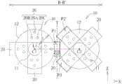
因此,本发明另提供另一实施例,请参考图6,不需要缩减各元件的尺寸,也不需要增加导光材的厚度,仅改变封装发光元件的排列方式,即可使得导光缆线之间排列得更紧密,进而节省空间。如图6所示,本实施例中,每一条导光缆线10周围同样包含四个封装发光元件20。但在导光缆线的一交界处(此处的交界处定义为导光缆线10之间距离最近的空隙处,也就是宽度G2的所在位置),发光元件20之间呈现错位排列。以本实施例为例,对于左方的导光缆线10,封装发光元件20仍分别设置在导电材11的正右方、正上方、正左方与正下方(例如分别沿着X-Z轴的角度0度、90度、180度与270度),而对于右方的导光缆线10,封装发光元件20则分别设置在导电材11的右斜上方、左斜上方、左斜下方与右斜下方(例如分别沿着X-Z轴的角度45度、135度、225度与315度)。值得注意的是,上述角度仅为本发明的一范例,若排列角度有局部调整也属于本发明的涵盖范围。Therefore, the present invention provides another embodiment, please refer to FIG. 6 , without reducing the size of each element or increasing the thickness of the light guide material, only changing the arrangement of the packaged light emitting elements, the light guide cable can be The spaces are arranged more closely, thereby saving space. As shown in FIG. 6 , in this embodiment, four encapsulated light-emitting
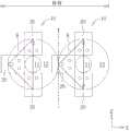
根据本实施例的排列方式,两个导光缆线10的圆心分别定义为中心C1与中心C2,且连接两中心C1、C2的连心线(虚拟连心线)定义为L1,另有一连心线L1的中垂线T定义于图上。其中,中垂线T与连心线L1垂直,且中垂线L上的任一位置至中心C1与中心C2的距离相等。在本实施例中,至少有一个封装发光元件20与中垂线T重叠。以图6为例,有三个封装发光元件20与中垂线T重叠。本实施例中,沿着中垂线T的方向,两导光缆线10上的各封装发光元件20彼此错位排列,从另一方面来看,两导光缆线10各自所包含的封装发光元件20并不沿着中垂线T左右对称排列。通过本发明改动封装发光元件20的排列,使得各封装发光元件20在交界处呈现错位排列,且左方导光缆线10的一突出部P1位于右方导光缆线10的一突出部P2与另一突出部P3之间,因此有效地利用突出部之间的空间,使得两导光缆线10之间的距离更近,也就是间隙宽度G2会较上述实施例的间隙宽度G1小,进而达到节省模块空间、或单位面积内封装发光元件数量增加、或发光强度增加等效果。According to the arrangement of this embodiment, the circle centers of the two
下方段落叙述本发明的其他实施例,尤其是针对其他封装发光元件的排列方式进行举例。值得注意的是,下方所述的各实施例中封装发光元件的排列方式仅为示例,而本发明不以此为限制,例如调整各实施例的封装发光元件的角度或位置,皆应属于本发明的含盖范围内。为简化说明,以下说明主要针对各实施例不同之处进行详述,而不再对相同之处作重复赘述。此外,本发明的各实施例中相同的元件是以相同的标号进行标示,以利于各实施例间互相对照。The following paragraphs describe other embodiments of the present invention, especially for the arrangement of other packaged light-emitting elements. It is worth noting that the arrangement of the packaged light-emitting elements in the embodiments described below is only an example, and the present invention is not limited to this. For example, adjusting the angle or position of the packaged light-emitting elements in each embodiment shall belong to this within the scope of the invention. In order to simplify the description, the following description mainly focuses on the differences between the embodiments, and does not repeat the same points. In addition, the same elements in the various embodiments of the present invention are marked with the same reference numerals, so as to facilitate mutual comparison among the various embodiments.
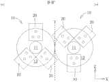
请参考图7,图7绘示本发明另一较佳实施例中封装发光元件的排列方式。为简化说明,此实施例以两条相邻的导光缆线进行说明,然而可理解的是本发明不限于此,而可能包含有更多条导光缆线。如图7所示,每一条导光缆线10周围仅设置一个封装发光元件20,而左方的封装发光元件20与右方的封装发光元件20排列的排列位置或是排列角度不同,并形成错位排列。在本实施例中,两导光缆线10可以直接接触,也就是两导光缆线之间的间距为0,但不限于此,两导光缆线10也可以相隔一段距离。另外,本实施例中,至少一个封装发光元件20同时与两个相邻的导光缆线10面积重叠,且本实施例同样满足至少有一个封装发光元件20与中垂线T重叠的条件(以本实施例为例,有两个封装发光元件20与中垂线T重叠)。此外值得注意的是,在一些实施例中,若两导光缆线10直接接触,此时中垂线T即与两导光缆线10的一内功切线相等。Please refer to FIG. 7 , which illustrates the arrangement of the packaged light-emitting elements in another preferred embodiment of the present invention. To simplify the description, this embodiment is described with two adjacent light guide cables, but it is understood that the present invention is not limited to this, and may include more light guide cables. As shown in FIG. 7 , only one packaged light-emitting
请参考图8,图8绘示本发明另一较佳实施例中封装发光元件的排列方式。为简化说明,此实施例以两条相邻的导光缆线进行说明,然而可理解的是本发明不限于此,而可能包含有更多条导光缆线。如图8所示,每一条导光缆线10周围设置两个封装发光元件20,而左方的封装发光元件20与右方的封装发光元件20排列的排列位置或是排列角度不同,例如左方的两个封装发光元件20沿着垂直方向(Z轴)排列,而右方的两个封装发光元件20沿着水平方向(X轴)排列,并形成错位排列。在本实施例中,两导光缆线10可以直接接触,也就是两导光缆线之间的间距为0,但不限于此,两导光缆线10也可以相隔一段距离。另外,本实施例中,至少一个封装发光元件20同时与两个相邻的导光缆线10面积重叠,且本实施例同样满足至少有一个封装发光元件20与中垂线T重叠的条件(以本实施例为例,有一个封装发光元件20与中垂线T重叠)。Please refer to FIG. 8 . FIG. 8 illustrates the arrangement of the packaged light-emitting elements in another preferred embodiment of the present invention. To simplify the description, this embodiment is described with two adjacent light guide cables, but it is understood that the present invention is not limited to this, and may include more light guide cables. As shown in FIG. 8 , two encapsulated light-emitting
请参考图9,图9绘示本发明另一较佳实施例中封装发光元件的排列方式。为简化说明,此实施例以两条相邻的导光缆线进行说明,然而可理解的是本发明不限于此,而可能包含有更多条导光缆线。如图9所示,每一条导光缆线10周围设置三个封装发光元件20,而左方的封装发光元件20与右方的封装发光元件20排列的排列位置或是排列角度不同,例如左方的三个封装发光元件20呈现正三角形排列,而右方的三个封装发光元件20呈现倒三角形排列,并形成错位排列。在本实施例中,两导光缆线10可以直接接触,也就是两导光缆线之间的间距为0,但不限于此,两导光缆线10也可以相隔一段距离。另外,本实施例同样满足至少有一个封装发光元件20与中垂线T重叠的条件(以本实施例为例,有两个封装发光元件20与中垂线T重叠)。Please refer to FIG. 9. FIG. 9 illustrates the arrangement of the packaged light-emitting elements in another preferred embodiment of the present invention. To simplify the description, this embodiment is described with two adjacent light guide cables, but it is understood that the present invention is not limited to this, and may include more light guide cables. As shown in FIG. 9 , three packaged light-emitting
请参考图10,图10绘示本发明另一较佳实施例中封装发光元件的排列方式。为简化说明,此实施例以两条相邻的导光缆线进行说明,然而可理解的是本发明不限于此,而可能包含有更多条导光缆线。如图10所示,每一条导光缆线10周围设置三个封装发光元件20。本实施例中,左方的封装发光元件20与右方的封装发光元件20排列的排列位置或是排列角度相同。虽然本实施例中并不形成上述“错位排列”,但是值得注意的是,从剖面方向来看,每一个导光缆线包含的多个封装发光元件20排列成一图案S,其中图案S为一非对称的形状。举例来说,如图10所示,每一个图案S沿着一垂直方向(也就是与中垂线T平行的方向)为非对称的图案,本实施例中每一个图案S为非对称的三角形图案,例如一个顶点在左侧的等腰三角形。也就是说本实施例中,每一条导光缆线的图案S都为同侧(也就是都同为顶点在左侧的等腰三角形),如此一来,在图案的排列上更为紧密,且有助于增加入光亮(因为固定面积内可容纳更多封装发光元件)。在本实施例中,两导光缆线10可以直接接触,也就是两导光缆线之间的间距为0,但不限于此,两导光缆线10也可以相隔一段距离。另外,本实施例中,至少一个封装发光元件20同时与两个相邻的导光缆线10面积重叠,且本实施例同样满足至少有一个封装发光元件20与中垂线T重叠的条件(以本实施例为例,有一个封装发光元件20与中垂线T重叠)。Please refer to FIG. 10 . FIG. 10 illustrates the arrangement of the packaged light-emitting elements in another preferred embodiment of the present invention. To simplify the description, this embodiment is described with two adjacent light guide cables, but it is understood that the present invention is not limited to this, and may include more light guide cables. As shown in FIG. 10 , three packaged light-emitting
值得注意的是,虽然上述实施例中,封装发光元件大多为平均排列分布,以达到光线均匀传导的效果,但本发明并不限定各封装发光元件必须要平均排列分布,而可以依照实际需求而调整封装发光元件的排列方式。It is worth noting that although most of the packaged light-emitting elements are evenly arranged and distributed in the above-mentioned embodiments to achieve the effect of uniform light transmission, the present invention does not limit that each packaged light-emitting element must be evenly arranged and distributed, and can be arranged according to actual needs. Adjust the arrangement of packaged light-emitting elements.
综上所述,若封装发光元件的排列符合以下条件的一项或多项,应属于本发明所述的排列:To sum up, if the arrangement of packaged light-emitting elements meets one or more of the following conditions, it should belong to the arrangement described in the present invention:
(1)对于两相邻的导光缆线,包含至少有一封装发光元件,与两个相邻的导光缆线的连心线的一中垂线重叠。(1) For two adjacent light guide cables, at least one packaged light-emitting element is included, which overlaps with a vertical line of the connecting center lines of the two adjacent light guide cables.
(2)对于两相邻的导光缆线,设置在周围的封装发光元件的排列位置或是排列角度不同。(2) For two adjacent light guide cables, the arrangement positions or arrangement angles of the encapsulated light-emitting elements arranged around are different.
(3)各导光缆线所包含的多个封装发光元件排列成相同的图案,其中该图案为一非对称图案(沿着垂直方向或是沿着中垂线方向)。(3) A plurality of packaged light-emitting elements included in each light-guiding cable are arranged in the same pattern, wherein the pattern is an asymmetric pattern (along the vertical direction or the direction of the mid-perpendicular line).
另外,在本发明的其他实施例中,也可以不形成体积较大的封装发光元件,而是直接将内部的发光单元(例如LED)形成在印刷电路板上,再通过壳体封装,进而达到防水防尘的效果。如此一来,将可以在有限的空间内容纳更多的发光元件。In addition, in other embodiments of the present invention, it is also possible not to form a bulky packaged light-emitting element, but to directly form an internal light-emitting unit (such as an LED) on a printed circuit board, and then encapsulate it through a housing to achieve Waterproof and dustproof effect. In this way, more light-emitting elements can be accommodated in a limited space.
本发明的特征在于,当每一条导光缆线的周围设置更多的封装发光元件,代表更强的光源可以照射至导光缆线的导光材内,增加软性发光线材的显示光效强度,且同时也提高光传导的距离。但是当导光缆线周围设置的封装发光元件数量增加时,也同时需要更多的空间去容纳该些导光缆线以及封装发光元件。因此本发明以改变封装发光元件的排列方式,不需要缩减各元件的尺寸,也不需要增加导光材的厚度,即可使得导光缆线之间排列得更紧密,进而节省空间。The present invention is characterized in that, when more encapsulated light-emitting elements are arranged around each light-guiding cable, it means that a stronger light source can be irradiated into the light-guiding material of the light-guiding cable, thereby increasing the display light effect intensity of the flexible light-emitting wire. At the same time, the distance of light transmission is also increased. However, when the number of packaged light-emitting elements disposed around the light-guiding cables increases, more space is also required to accommodate the light-guiding cables and the packaged light-emitting elements. Therefore, the present invention changes the arrangement of the packaged light-emitting elements without reducing the size of each element or increasing the thickness of the light-guiding material, so that the light-guiding cables can be arranged more closely, thereby saving space.
以上所述仅为本发明的较佳实施例,凡依本发明权利要求所做的均等变化与修饰,皆应属本发明的涵盖范围。The above descriptions are only preferred embodiments of the present invention, and all equivalent changes and modifications made according to the claims of the present invention shall fall within the scope of the present invention.
Claims (18)
Applications Claiming Priority (2)
| Application Number | Priority Date | Filing Date | Title |
|---|---|---|---|
| TW108119542ATWI681143B (en) | 2019-06-05 | 2019-06-05 | Flexible illuminating cable |
| TW108119542 | 2019-06-05 |
Publications (1)
| Publication Number | Publication Date |
|---|---|
| CN112050097Atrue CN112050097A (en) | 2020-12-08 |
Family
ID=69942636
Family Applications (1)
| Application Number | Title | Priority Date | Filing Date |
|---|---|---|---|
| CN201910604259.XAPendingCN112050097A (en) | 2019-06-05 | 2019-07-05 | Luminous line group |
Country Status (3)
| Country | Link |
|---|---|
| US (1) | US10890713B2 (en) |
| CN (1) | CN112050097A (en) |
| TW (1) | TWI681143B (en) |
Families Citing this family (1)
| Publication number | Priority date | Publication date | Assignee | Title |
|---|---|---|---|---|
| USD1009311S1 (en)* | 2022-02-18 | 2023-12-26 | Dongguan Xingyang Technology Co., Ltd. | Light-emitting device |
Citations (5)
| Publication number | Priority date | Publication date | Assignee | Title |
|---|---|---|---|---|
| US5859945A (en)* | 1996-04-01 | 1999-01-12 | Sumitomo Electric Industries, Ltd. | Array type light emitting element module and manufacturing method therefor |
| CN2876546Y (en)* | 2005-08-18 | 2007-03-07 | 付刚 | Light guiding plate |
| CN202074422U (en)* | 2011-03-28 | 2011-12-14 | 上海向隆电子科技有限公司 | Light source device |
| US20120039070A1 (en)* | 2010-08-13 | 2012-02-16 | Taiwan Textile Research Institute | Linear light-emitting module and textile product having the same |
| TWM572585U (en)* | 2018-09-20 | 2019-01-01 | 大昱光電股份有限公司 | Soft lighting cable |
Family Cites Families (7)
| Publication number | Priority date | Publication date | Assignee | Title |
|---|---|---|---|---|
| US5790733A (en)* | 1996-06-07 | 1998-08-04 | Minnesota Mining And Manufactouring Company | Optoelectronic device receptacle and method of making same |
| TWI579611B (en)* | 2015-11-02 | 2017-04-21 | 峰川光電股份有限公司 | Photoelectric conversion assembly |
| TWI598653B (en)* | 2016-03-16 | 2017-09-11 | 峰川光電股份有限公司 | Photoelectric conversion assembly |
| TWM545379U (en)* | 2017-02-22 | 2017-07-11 | Energy Full Electronics Co Ltd | Flexible and luminescent flat cable |
| US10649168B2 (en)* | 2017-05-31 | 2020-05-12 | Molex, Llc | Illuminated tracer cable |
| US10069252B1 (en)* | 2018-03-08 | 2018-09-04 | Chia-Hua Lin | Plug structure of light emitting AC electric power cord |
| TWI662226B (en)* | 2018-09-20 | 2019-06-11 | 大昱光電股份有限公司 | Flexible illuminating cable for power module |
- 2019
- 2019-06-05TWTW108119542Apatent/TWI681143B/ennot_activeIP Right Cessation
- 2019-07-05CNCN201910604259.XApatent/CN112050097A/enactivePending
- 2019-07-25USUS16/521,595patent/US10890713B2/ennot_activeExpired - Fee Related
Patent Citations (5)
| Publication number | Priority date | Publication date | Assignee | Title |
|---|---|---|---|---|
| US5859945A (en)* | 1996-04-01 | 1999-01-12 | Sumitomo Electric Industries, Ltd. | Array type light emitting element module and manufacturing method therefor |
| CN2876546Y (en)* | 2005-08-18 | 2007-03-07 | 付刚 | Light guiding plate |
| US20120039070A1 (en)* | 2010-08-13 | 2012-02-16 | Taiwan Textile Research Institute | Linear light-emitting module and textile product having the same |
| CN202074422U (en)* | 2011-03-28 | 2011-12-14 | 上海向隆电子科技有限公司 | Light source device |
| TWM572585U (en)* | 2018-09-20 | 2019-01-01 | 大昱光電股份有限公司 | Soft lighting cable |
Also Published As
| Publication number | Publication date |
|---|---|
| US20200386940A1 (en) | 2020-12-10 |
| US10890713B2 (en) | 2021-01-12 |
| TWI681143B (en) | 2020-01-01 |
| TW202045853A (en) | 2020-12-16 |
Similar Documents
| Publication | Publication Date | Title |
|---|---|---|
| US10711971B2 (en) | Vehicle light assembly comprising flexible lighting strip | |
| US6392342B1 (en) | Light source arrangement for planar applications | |
| US20200066698A1 (en) | Light-emitting module and tandem light-emitting device | |
| US20040042735A1 (en) | Illuminant USB cable | |
| US11248758B2 (en) | Surface light source LED device | |
| US20170051904A1 (en) | Direct-type LED Backlight Module | |
| CN111627737A (en) | Backlight module | |
| TWM545379U (en) | Flexible and luminescent flat cable | |
| CN106813161A (en) | A kind of luminescence component and mobile terminal | |
| US20040071410A1 (en) | Illuminant USB cable | |
| TW202012828A (en) | Flexible illuminating cable for power module | |
| CN112050097A (en) | Luminous line group | |
| CN210627943U (en) | lighted cable | |
| CN213691839U (en) | Backlight module and backlight keyboard using same | |
| CN210296810U (en) | Light-emitting cable structure | |
| CN209880986U (en) | Luminous cable structure | |
| CN209786372U (en) | Light-emitting flat cable structure | |
| CN210092494U (en) | Light-emitting cable structure | |
| CN222355663U (en) | Luminous cable structure | |
| US20210041614A1 (en) | Display device and operation method thereof | |
| WO2020155087A1 (en) | Light-emitting cable structure | |
| WO2021046813A1 (en) | Light-emitting cable structure | |
| CN218762753U (en) | Light guide structure, light source device and electronic equipment | |
| JP2000029024A (en) | Backlight device for liquid crystal panel | |
| TWM592174U (en) | Luminescent flat cable |
Legal Events
| Date | Code | Title | Description |
|---|---|---|---|
| PB01 | Publication | ||
| PB01 | Publication | ||
| SE01 | Entry into force of request for substantive examination | ||
| SE01 | Entry into force of request for substantive examination | ||
| TA01 | Transfer of patent application right | ||
| TA01 | Transfer of patent application right | Effective date of registration:20201228 Address after:Taoyuan City, Taiwan, China Applicant after:Pinhui Technology Co.,Ltd. Address before:Taoyuan City, Taiwan, China Applicant before:DAYU OPTOELECTRONICS Co.,Ltd. | |
| AD01 | Patent right deemed abandoned | ||
| AD01 | Patent right deemed abandoned | Effective date of abandoning:20230811 |