CN112038091B - Adjustable capacitor based on MEMS structure - Google Patents
Adjustable capacitor based on MEMS structureDownload PDFInfo
- Publication number
- CN112038091B CN112038091BCN202010771747.2ACN202010771747ACN112038091BCN 112038091 BCN112038091 BCN 112038091BCN 202010771747 ACN202010771747 ACN 202010771747ACN 112038091 BCN112038091 BCN 112038091B
- Authority
- CN
- China
- Prior art keywords
- electrode
- capacitor
- adjusting
- adjustable
- movable
- Prior art date
- Legal status (The legal status is an assumption and is not a legal conclusion. Google has not performed a legal analysis and makes no representation as to the accuracy of the status listed.)
- Active
Links
- 239000003990capacitorSubstances0.000titleclaimsabstractdescription367
- 239000004020conductorSubstances0.000claimsabstractdescription110
- 239000010410layerSubstances0.000claimsdescription83
- 239000003989dielectric materialSubstances0.000claimsdescription40
- 239000002184metalSubstances0.000claimsdescription36
- 239000011159matrix materialSubstances0.000claimsdescription17
- 239000000758substrateSubstances0.000claimsdescription9
- 238000004806packaging method and processMethods0.000claimsdescription7
- 239000000463materialSubstances0.000claimsdescription6
- 238000005538encapsulationMethods0.000claimsdescription5
- 239000007769metal materialSubstances0.000claimsdescription4
- 238000003860storageMethods0.000claimsdescription4
- 238000007906compressionMethods0.000claimsdescription3
- 239000002356single layerSubstances0.000claimsdescription3
- 230000003068static effectEffects0.000claimsdescription2
- 238000003466weldingMethods0.000claimsdescription2
- 230000006835compressionEffects0.000claims1
- 229910052755nonmetalInorganic materials0.000claims1
- 230000010355oscillationEffects0.000claims1
- 238000010586diagramMethods0.000description20
- 238000000034methodMethods0.000description20
- 230000008569processEffects0.000description13
- 238000002955isolationMethods0.000description12
- WABPQHHGFIMREM-UHFFFAOYSA-Nlead(0)Chemical compound[Pb]WABPQHHGFIMREM-UHFFFAOYSA-N0.000description11
- 229910021421monocrystalline siliconInorganic materials0.000description8
- 238000004544sputter depositionMethods0.000description8
- 230000008859changeEffects0.000description7
- 230000003071parasitic effectEffects0.000description4
- 229910000679solderInorganic materials0.000description4
- 238000000151depositionMethods0.000description3
- 230000008021depositionEffects0.000description3
- 238000005530etchingMethods0.000description3
- 230000006870functionEffects0.000description3
- 230000001276controlling effectEffects0.000description2
- 230000000694effectsEffects0.000description2
- 230000005684electric fieldEffects0.000description2
- 230000001681protective effectEffects0.000description2
- 239000011241protective layerSubstances0.000description2
- 239000004065semiconductorSubstances0.000description2
- FGRBYDKOBBBPOI-UHFFFAOYSA-N10,10-dioxo-2-[4-(N-phenylanilino)phenyl]thioxanthen-9-oneChemical compoundO=C1c2ccccc2S(=O)(=O)c2ccc(cc12)-c1ccc(cc1)N(c1ccccc1)c1ccccc1FGRBYDKOBBBPOI-UHFFFAOYSA-N0.000description1
- 230000009471actionEffects0.000description1
- 230000002929anti-fatigueEffects0.000description1
- 238000005452bendingMethods0.000description1
- 230000009286beneficial effectEffects0.000description1
- 239000011248coating agentSubstances0.000description1
- 238000000576coating methodMethods0.000description1
- 238000010276constructionMethods0.000description1
- 238000002788crimpingMethods0.000description1
- 229910021419crystalline siliconInorganic materials0.000description1
- 230000007547defectEffects0.000description1
- 230000004069differentiationEffects0.000description1
- 238000009826distributionMethods0.000description1
- 230000002708enhancing effectEffects0.000description1
- 239000005022packaging materialSubstances0.000description1
- 230000002093peripheral effectEffects0.000description1
- 230000001105regulatory effectEffects0.000description1
- 238000006467substitution reactionMethods0.000description1
- 239000002344surface layerSubstances0.000description1
Images


Classifications
- H—ELECTRICITY
- H01—ELECTRIC ELEMENTS
- H01G—CAPACITORS; CAPACITORS, RECTIFIERS, DETECTORS, SWITCHING DEVICES, LIGHT-SENSITIVE OR TEMPERATURE-SENSITIVE DEVICES OF THE ELECTROLYTIC TYPE
- H01G5/00—Capacitors in which the capacitance is varied by mechanical means, e.g. by turning a shaft; Processes of their manufacture
- H01G5/38—Multiple capacitors, e.g. ganged
- G—PHYSICS
- G02—OPTICS
- G02B—OPTICAL ELEMENTS, SYSTEMS OR APPARATUS
- G02B26/00—Optical devices or arrangements for the control of light using movable or deformable optical elements
- G02B26/08—Optical devices or arrangements for the control of light using movable or deformable optical elements for controlling the direction of light
- G02B26/0816—Optical devices or arrangements for the control of light using movable or deformable optical elements for controlling the direction of light by means of one or more reflecting elements
- G02B26/0833—Optical devices or arrangements for the control of light using movable or deformable optical elements for controlling the direction of light by means of one or more reflecting elements the reflecting element being a micromechanical device, e.g. a MEMS mirror, DMD
- G02B26/0841—Optical devices or arrangements for the control of light using movable or deformable optical elements for controlling the direction of light by means of one or more reflecting elements the reflecting element being a micromechanical device, e.g. a MEMS mirror, DMD the reflecting element being moved or deformed by electrostatic means
- H—ELECTRICITY
- H01—ELECTRIC ELEMENTS
- H01G—CAPACITORS; CAPACITORS, RECTIFIERS, DETECTORS, SWITCHING DEVICES, LIGHT-SENSITIVE OR TEMPERATURE-SENSITIVE DEVICES OF THE ELECTROLYTIC TYPE
- H01G5/00—Capacitors in which the capacitance is varied by mechanical means, e.g. by turning a shaft; Processes of their manufacture
- H01G5/01—Details
- H01G5/011—Electrodes
- H—ELECTRICITY
- H01—ELECTRIC ELEMENTS
- H01G—CAPACITORS; CAPACITORS, RECTIFIERS, DETECTORS, SWITCHING DEVICES, LIGHT-SENSITIVE OR TEMPERATURE-SENSITIVE DEVICES OF THE ELECTROLYTIC TYPE
- H01G5/00—Capacitors in which the capacitance is varied by mechanical means, e.g. by turning a shaft; Processes of their manufacture
- H01G5/01—Details
- H01G5/013—Dielectrics
- H—ELECTRICITY
- H01—ELECTRIC ELEMENTS
- H01G—CAPACITORS; CAPACITORS, RECTIFIERS, DETECTORS, SWITCHING DEVICES, LIGHT-SENSITIVE OR TEMPERATURE-SENSITIVE DEVICES OF THE ELECTROLYTIC TYPE
- H01G5/00—Capacitors in which the capacitance is varied by mechanical means, e.g. by turning a shaft; Processes of their manufacture
- H01G5/16—Capacitors in which the capacitance is varied by mechanical means, e.g. by turning a shaft; Processes of their manufacture using variation of distance between electrodes
- H—ELECTRICITY
- H01—ELECTRIC ELEMENTS
- H01G—CAPACITORS; CAPACITORS, RECTIFIERS, DETECTORS, SWITCHING DEVICES, LIGHT-SENSITIVE OR TEMPERATURE-SENSITIVE DEVICES OF THE ELECTROLYTIC TYPE
- H01G5/00—Capacitors in which the capacitance is varied by mechanical means, e.g. by turning a shaft; Processes of their manufacture
- H01G5/40—Structural combinations of variable capacitors with other electric elements not covered by this subclass, the structure mainly consisting of a capacitor, e.g. RC combinations
Landscapes
- Engineering & Computer Science (AREA)
- Power Engineering (AREA)
- Microelectronics & Electronic Packaging (AREA)
- Physics & Mathematics (AREA)
- General Physics & Mathematics (AREA)
- Optics & Photonics (AREA)
- Micromachines (AREA)
- Fixed Capacitors And Capacitor Manufacturing Machines (AREA)
Abstract
Translated fromChinese
Description
Translated fromChinese技术领域technical field
本发明属于电容器件技术领域,具体涉及一种基于MEMS结构的可调电容。The invention belongs to the technical field of capacitor devices, in particular to an adjustable capacitor based on a MEMS structure.
背景技术Background technique
现有射频电路应用中,经常需要使同一射频电路工作在不同的工作频段,由于射频电路工作在不同的频段时其对应的匹配电路的电容容值需要做相应的调整,才能获得最佳的射频性能,因此为了使射频电路工作在不同的频段,需要对射频电路中匹配电容的参数值进行调整,在这一类射频电路中采用可调电容是最合适的设计方案,现有可调电容实现的方式有四种:第一种是用变容二极管实现电容的可调,通过调整变容二极管的偏置电压值可实现变容二极管电容值的调整,然而采用变容二极管存在的问题是其耐压值比较低,只能应用在小功率射频电路中,不能满足射频大功率放大器中大功率高耐压的要求;第二种可调电容的实现方案是采用机械可变电容,通过调整电容上、下极板的机械尺寸或者间距来调整电容的容值,采用纯机械结构实现的可调电容方案存在的问题是,可调电容的体积比较大、电容的可调步进和可调范围有限、不能实现实时可调等不足;第三种可调电容的实现方案是采用由多组电容串联或者并联,并在串、并联线路中间串上射频开关,通过控制射频开关的通断来实现不同串联或者并联电容的组合,方案三的缺点是由于可调电容需要高耐压和耐流值,因此对应的开关也需要选用大功率的开关,其对应的成本偏高,同时开关会带来额外的损耗影响效率,另外方案三的可调范围和可调步进固定死了不能变化,或者不能任意变化可调,方案四是采用介质开关型MEMS电容,通常触点臂为电容的一端,当电路应用有较高直流偏置时,触点臂与电容另一端会产生静电引力,给开关电容开启带来困难;同时,由于触点弯曲、形变使得闭合时电容相对减小。针对以上各种可调电容存在的问题,开发出一款容值步进任意可调,同时具备高Q值、高耐压值、小体积低成本的可调电容是一个值得深入研究的课题。In the existing RF circuit applications, it is often necessary to make the same RF circuit work in different working frequency bands. Since the RF circuit works in different frequency bands, the capacitance value of the corresponding matching circuit needs to be adjusted accordingly to obtain the best RF frequency. Therefore, in order to make the radio frequency circuit work in different frequency bands, the parameter value of the matching capacitor in the radio frequency circuit needs to be adjusted. In this type of radio frequency circuit, the use of adjustable capacitors is the most suitable design scheme. There are four ways: the first is to use a varactor diode to adjust the capacitance. By adjusting the bias voltage value of the varactor diode, the capacitance value of the varactor diode can be adjusted. However, the problem of using a varactor diode is its The withstand voltage value is relatively low, and can only be used in low-power radio frequency circuits, which cannot meet the requirements of high power and high withstand voltage in radio frequency high-power amplifiers; the second implementation scheme of adjustable capacitors is to use mechanical variable capacitors. The mechanical size or spacing of the upper and lower plates is used to adjust the capacitance value of the capacitor. The problems of the adjustable capacitor scheme realized by pure mechanical structure are that the volume of the adjustable capacitor is relatively large, and the adjustable step and range of the capacitor are adjustable. Limited, unable to realize real-time adjustment and other shortcomings; the third implementation scheme of adjustable capacitors is to use multiple groups of capacitors in series or parallel, and connect a radio frequency switch in the middle of the series and parallel lines, and realize by controlling the on-off of the radio frequency switch. Combinations of different series or parallel capacitors, the disadvantage of the third solution is that since the adjustable capacitor requires high withstand voltage and current withstand value, the corresponding switch also needs to use a high-power switch, and the corresponding cost is high, and the switch will bring The additional loss affects the efficiency. In addition, the adjustable range and adjustable step of the third solution cannot be changed, or can not be adjusted arbitrarily. The fourth solution is to use a dielectric switch type MEMS capacitor, usually the contact arm is one end of the capacitor. When a high DC bias is applied to the circuit, electrostatic attraction will be generated between the contact arm and the other end of the capacitor, making it difficult to open the switched capacitor; at the same time, due to the bending and deformation of the contact, the capacitance is relatively reduced when it is closed. In view of the above problems of various adjustable capacitors, it is a topic worthy of in-depth study to develop an adjustable capacitor whose capacitance value can be adjusted arbitrarily, with high Q value, high withstand voltage value, small size and low cost.
发明内容SUMMARY OF THE INVENTION
本发明的目的是针对现有可调电容的缺陷,提供一种具备高Q值、高耐压值、小体积、低成本的可调电容。The purpose of the present invention is to provide an adjustable capacitor with high Q value, high withstand voltage value, small size and low cost in view of the defects of the existing adjustable capacitor.
为此,本发明的构成是,包括下极板A,活动极板B、上极板C、固定装置D和连接线导体E,所述固定装置D的下端与下极板A固定连接,固定装置D的上端与上极板C固定连接,活动极板B通过结构B4安装于固定装置D上并且活动极板B能沿固定装置D进行上、下移动;For this reason, the structure of the present invention is to include a lower pole plate A, a movable pole plate B, an upper pole plate C, a fixing device D and a connecting wire conductor E, and the lower end of the fixing device D is fixedly connected with the lower pole plate A, fixed The upper end of the device D is fixedly connected with the upper pole plate C, the movable pole plate B is installed on the fixing device D through the structure B4, and the movable pole plate B can move up and down along the fixing device D;
所述下极板A上设置有下电极A1,所述活动极板B上设置有活动电极B1,调整电极B2;The lower electrode plate A is provided with a lower electrode A1, the movable electrode plate B is provided with a movable electrode B1, and an adjustment electrode B2;
所述下电极A1与活动电极B1组成单元电容,且下电极A1和活动电极B1之间通过介质隔离;The lower electrode A1 and the movable electrode B1 form a unit capacitor, and the lower electrode A1 and the movable electrode B1 are separated by a medium;
所述上极板C上设置有上电极C1、调整电极C2;所述连接线导体E两端分别与上电极C1、活动电极B1电连接;The upper electrode plate C is provided with an upper electrode C1 and an adjustment electrode C2; both ends of the connecting wire conductor E are respectively electrically connected to the upper electrode C1 and the movable electrode B1;
所述调整电极C2与调整电极B2组成调整单元,且调整电极C2和调整电极B2 之间通过介质隔离;The adjustment electrode C2 and the adjustment electrode B2 form an adjustment unit, and the adjustment electrode C2 and the adjustment electrode B2 are separated by a medium;
所述下电极A1在工作状态下一直加有工作电压,工作电压对活动电极B1产生静电吸引力,通过控制调整电极C2上所加可调电压来调节调整电极C2对调整电极 B2的静电吸引力,使活动极板B受下电极A1的吸引力与调整电极C2的吸引力的大小关系发生改变,从而使活动极板B沿固定装置D上、下移动调整电容的容值。The lower electrode A1 is always supplied with a working voltage in the working state, and the working voltage produces an electrostatic attraction to the movable electrode B1, and the electrostatic attraction of the adjustment electrode C2 to the adjustment electrode B2 is adjusted by controlling the adjustable voltage applied on the adjustment electrode C2. , so that the relationship between the attractive force of the lower electrode A1 and the attractive force of the adjusting electrode C2 is changed by the movable electrode plate B, so that the movable electrode plate B moves up and down along the fixing device D to adjust the capacitance value of the capacitor.
优选地,所述下电极A1与活动电极B1组成单元电容,所述下电极A1上设置有介质层A2用于隔离下电极A1和活动电极B1。Preferably, the lower electrode A1 and the movable electrode B1 form a unit capacitor, and a dielectric layer A2 is provided on the lower electrode A1 for isolating the lower electrode A1 and the movable electrode B1.
优选地,所述调整电极C2与调整电极B2组成调整单元,且调整电极C2上设置有介质层C3用于隔离调整电极C2和调整电极B2,调整电极C2与活动电极B1、下电极A1不重叠,调整电极B2与上电极C1和下电极A1不重叠。Preferably, the adjustment electrode C2 and the adjustment electrode B2 form an adjustment unit, and the adjustment electrode C2 is provided with a dielectric layer C3 for isolating the adjustment electrode C2 and the adjustment electrode B2, and the adjustment electrode C2 does not overlap with the movable electrode B1 and the lower electrode A1 , the adjustment electrode B2 does not overlap with the upper electrode C1 and the lower electrode A1.
优选地,所述下极板A由介质材料构成,在下极板A的介质材料表面覆盖或镶嵌有金属导体形成下电极A1,在下电极A1表面设置有单层或者多层介质材料层A2,用于隔离下电极A1和活动电极B1,同时可以调节电容的容值和Q值。Preferably, the lower electrode plate A is made of a dielectric material, and the surface of the dielectric material of the lower electrode plate A is covered or embedded with metal conductors to form the lower electrode A1, and a single-layer or multi-layer dielectric material layer A2 is provided on the surface of the lower electrode A1. In order to isolate the lower electrode A1 and the active electrode B1, the capacitance and Q value of the capacitor can be adjusted at the same time.
优选地,所述活动极板B由介质材料构成,在活动极板B的介质材料表面上覆盖或镶嵌有金属导体形成活动电极B1、调整电极B2,调整电极B2分布在活动电极 B1的外围且相互之间通过介质隔离,活动电极B1与下电极A1、上电极C1形状相同,在垂直面上对齐,调整电极B2和调整电极C2形状相同在垂直面上对齐。Preferably, the movable electrode plate B is made of a dielectric material, and metal conductors are covered or embedded on the surface of the dielectric material of the movable electrode plate B to form the movable electrode B1 and the adjustment electrode B2, and the adjustment electrode B2 is distributed on the periphery of the movable electrode B1 and Separated by a medium, the movable electrode B1 has the same shape as the lower electrode A1 and the upper electrode C1 and is aligned on the vertical plane, and the adjusting electrode B2 and the adjusting electrode C2 have the same shape and are aligned on the vertical plane.
优选地,所述上极板C由介质材料构成,在上极板C的介质材料表面覆盖或镶嵌有金属导体形成上电极C1,在上电极C1的外围介质材料表面覆盖或镶嵌金属导体形成调整电极C2,上电极C1和调整电极C2之间由介质材料隔离,调整电极C2表面设置有介质层C3,在上极板C设置有控制层C4,调整电极C2与控制层C4中开关的一端相连,开关的另一端连接到可调单元电容的可调电压引脚,所述单元电容通过活动极板B与调整单元组成可调单元电容。Preferably, the upper electrode plate C is made of a dielectric material, the surface of the dielectric material of the upper electrode plate C is covered or embedded with metal conductors to form the upper electrode C1, and the surface of the peripheral dielectric material of the upper electrode C1 is covered or embedded with metal conductors to form the adjustment The electrode C2, the upper electrode C1 and the adjustment electrode C2 are separated by a dielectric material, the surface of the adjustment electrode C2 is provided with a dielectric layer C3, the upper plate C is provided with a control layer C4, and the adjustment electrode C2 is connected with one end of the switch in the control layer C4 , the other end of the switch is connected to the adjustable voltage pin of the adjustable unit capacitor, and the unit capacitor forms the adjustable unit capacitor through the movable plate B and the adjustment unit.
优选地,所述固定装置D的一端与上极板C的上电极C1固定在一起,另一端与下极板A的下电极A1固定在一起,用于支撑上极板C和下极板A,保持上、下极板之间平行,其固定方式包括焊接、压接、粘接。Preferably, one end of the fixing device D is fixed with the upper electrode C1 of the upper electrode plate C, and the other end is fixed with the lower electrode A1 of the lower electrode plate A, so as to support the upper electrode plate C and the lower electrode plate A , keep the upper and lower plates parallel, and the fixing methods include welding, crimping and bonding.
优选地,所述连接线导体E由1至M根连接线导体组成;所述活动电极B1的上表面对应设计有1至M个开槽,所述上电极C1的下表面对应设置有1至M个开槽;所述的1至M根连接线导体的一端与上电极C1下表面的1至M个开槽电连接,1至 M根连接线导体的另一端与活动电极B1上表面的1至M个开槽电连接;由1至M根连线将上电极C1和活动电极B1电连接,1至M根连接线的电阻值越小越好,1至M 根连接线导体的长度相等使活动极板在自然状态下能与上极板、下极板保持平行。Preferably, the connecting wire conductor E is composed of 1 to M connecting wire conductors; the upper surface of the movable electrode B1 is correspondingly designed with 1 to M slots, and the lower surface of the upper electrode C1 is correspondingly provided with 1 to M slots. M slots; one end of the 1 to M connecting wire conductors is electrically connected to the 1 to M slots on the lower surface of the upper electrode C1, and the other end of the 1 to M connecting wire conductors is electrically connected to the upper surface of the movable electrode B1. 1 to M slotted electrical connections; the upper electrode C1 and the movable electrode B1 are electrically connected by 1 to M connecting lines, the resistance value of the 1 to M connecting lines is as small as possible, and the length of the conductors of the 1 to M connecting lines is The equalization makes the movable pole plate parallel to the upper pole plate and the lower pole plate in the natural state.
优选地,所述连接线导体E在静止或活动状态下与调整电极C2、B2都不短路;所述连接线导体E具备伸缩性能,其拉伸和弹力保持不变,其尺寸能满足使活动极板B被压缩时能与上极板C紧贴,向下被拉伸时能与下极板A紧贴。Preferably, the connecting wire conductor E is not short-circuited with the adjusting electrodes C2 and B2 in the static or active state; the connecting wire conductor E has stretchability, its stretching and elastic force remain unchanged, and its size can meet the requirements of making the moving When the electrode plate B is compressed, it can be in close contact with the upper electrode plate C, and when it is stretched downward, it can be in close contact with the lower electrode plate A.
优选地,所述连接线导体E、下电极A1、活动电极B1,调整电极B2、上电极C1、调整电极C2均是由金属材料制成,所述上极板A、活动极板B、下极板C的基板板材均为介质材料构成。Preferably, the connecting wire conductor E, the lower electrode A1, the movable electrode B1, the adjustment electrode B2, the upper electrode C1 and the adjustment electrode C2 are all made of metal materials. The substrate plates of the electrode plate C are all made of dielectric materials.
优选地,所述单元电容通过活动极板B与调整单元组成可调单元电容,所述下电极A1加工作电压后对活动电极B1产生的静电吸引力为Fx,调整电极C2加可调电压后对调整电极B2产生的静电吸引力为Fs,当Fs小于Fx时,活动极板B移向并贴近下极板A,此时可调单元电容的容值最大;当Fs大于Fx时,活动极板B移向并贴近上极板C,此时可调单元电容的容值最小;当调整电极C2所加可调电压为零,下电极A1所加工作电压不为零时,使活动极板B移向下极板A,保持可调单元电容处于容值最大状态。Preferably, the unit capacitor forms an adjustable unit capacitor through the movable electrode plate B and the adjustment unit, and the electrostatic attraction generated by the lower electrode A1 to the movable electrode B1 after applying the working voltage is Fx, and the adjustment electrode C2 after applying the adjustable voltage The electrostatic attraction to the adjustment electrode B2 is Fs. When Fs is less than Fx, the movable electrode B moves to and close to the lower electrode A, and the capacitance of the adjustable unit capacitor is the largest; when Fs is greater than Fx, the movable electrode Plate B moves to and close to the upper plate C, at this time the capacitance of the adjustable unit capacitor is the smallest; when the adjustable voltage applied by the adjustment electrode C2 is zero, and the working voltage applied by the lower electrode A1 is not zero, the movable plate Move B to the bottom plate A to keep the adjustable unit capacitor in the state of maximum capacitance.
优选地,所述单元电容通过活动极板B与调整单元组成可调单元电容,可调单元电容中下电极A1连接到工作电压引脚、上电极C1连接到接地引脚、调整电极C2 通过金属过孔连接到控制层C4上的开关的一端,开关的另一端连接到可调电压引脚,开关数据收发总线连接到控制引脚,处理器通过总线控制开关的通断和可调电压引脚上的电压来控制可调单元电容中活动极板B的移动,从而改变可调单元电容的容值。Preferably, the unit capacitor forms an adjustable unit capacitor through the movable electrode plate B and the adjustment unit. In the adjustable unit capacitor, the lower electrode A1 is connected to the working voltage pin, the upper electrode C1 is connected to the ground pin, and the adjustment electrode C2 is connected to the metal The via is connected to one end of the switch on the control layer C4, the other end of the switch is connected to the adjustable voltage pin, the switch data transceiver bus is connected to the control pin, and the processor controls the on-off of the switch and the adjustable voltage pin through the bus The voltage on the adjustable unit capacitor is used to control the movement of the movable plate B in the adjustable unit capacitor, thereby changing the capacitance value of the adjustable unit capacitor.
优选地,采用非金属材料封装上、下极板,留出电容的两个引脚,并标记接地引脚、工作电压引脚或控制引脚,控制引脚在电容引脚空出的位置或放置在其中接地引脚中的空隙位置作为控制引脚,最后封装密封,或者以上极板C和下极板A作为器件封装的一部分,外加封装材料实现对MEMS电容的封装。Preferably, the upper and lower plates are encapsulated with non-metallic materials, leaving two pins of the capacitor, and marking the ground pin, the working voltage pin or the control pin, and the control pin is in the vacated position of the capacitor pin or The voids placed in the ground pins are used as control pins, and finally the package is sealed, or the upper plate C and the lower plate A are used as part of the device package, and packaging materials are added to realize the packaging of the MEMS capacitor.
优选地,通过设置下电极A1上覆盖介质材料层A2的形状、厚度参数,使两路信号的幅度相等、相位相反,互相抵消或防止加射频信号后产生的谐振。Preferably, by setting the shape and thickness parameters of the dielectric material layer A2 covering the lower electrode A1, the amplitudes of the two signals are equal and the phases are opposite to cancel each other or prevent the resonance generated by adding the radio frequency signal.
优选地,N个所述可调单元电容组成组合电容。Preferably, the N adjustable unit capacitors form a combined capacitor.
优选地,所述组合电容的构成方式之一是N个可调单元电容纵向叠加构成一个组合电容,其中N个单元电容的下电极A1通过引出线连接到组合电容的工作电压引脚,N个单元电容的上电极C1通过引出线连接到组合电容的接地引脚,N个单元电容的调整电极C2分别通过引出线连接到N个单元电容上极板的N个开关的一端,N 个开关的另一端引出到组合电容的N个可调电压控制引脚之一,N个下电极A1都接到一个工作电压引脚,N个上电极C1都连接到地。Preferably, one of the construction methods of the combined capacitor is that N adjustable unit capacitors are vertically stacked to form a combined capacitor, wherein the lower electrode A1 of the N unit capacitors is connected to the working voltage pin of the combined capacitor through a lead wire, and the N The upper electrode C1 of the unit capacitor is connected to the ground pin of the combined capacitor through the lead wire, and the adjustment electrodes C2 of the N unit capacitors are respectively connected to one end of the N switches on the upper plate of the N unit capacitors through the lead wire. The other end leads to one of the N adjustable voltage control pins of the combined capacitor, the N lower electrodes A1 are all connected to a working voltage pin, and the N upper electrodes C1 are all connected to the ground.
优选地,所述组合电容的组合构成方式之二是组合电容中N个上电极C1分布在一个上极板C上,并通过引线连接至组合电容的接地引脚,N个下电极A1分布在一个下极板A上,并通过引线连接至组合电容的工作电压引脚,N个调整电极C2分别通过金属过孔连接至控制层C4上分布的N个开关的一端,N个开关的另一端连接至组合电容的N个可调电压控制引脚,所有的引线与上电极C1、活动电极B1、下电极A1不重叠。Preferably, the second combination method of the combined capacitor is that in the combined capacitor, N upper electrodes C1 are distributed on one upper electrode plate C, and are connected to the ground pin of the combined capacitor through leads, and N lower electrodes A1 are distributed on the A lower plate A is connected to the working voltage pin of the combined capacitor through a lead, and the N adjustment electrodes C2 are respectively connected to one end of the N switches distributed on the control layer C4 through metal vias, and the other end of the N switches Connected to the N adjustable voltage control pins of the combined capacitor, all the leads do not overlap with the upper electrode C1, the active electrode B1, and the lower electrode A1.
优选地,所述组合电容的构成之三是先M个单元电容按照构成方式之二的方式横向扩展,N个由M个单元电容横向扩展的组合电容再纵向叠加扩展构成新的组合电容,新的组合电容的每层的M个单元电容的M个上电极C1通过引线连接在一起后连接到组合电容的接地引脚,M个下电极A1通过引线连接在一起后连接到组合电容的工作电压引脚,M个调整电极C2分别连接到M个开关的一端,M个开关的另一端分别通过引线连接至组合电容的M个可调电压控制引脚,组合电容共有M*N 个可调电压引脚。Preferably, the third configuration of the combined capacitor is to firstly expand the M unit capacitors horizontally according to the second configuration method, and then the N combined capacitors that are horizontally expanded by the M unit capacitors are vertically stacked to form a new combined capacitor. The M upper electrodes C1 of the M unit capacitors of each layer of the combined capacitor are connected together by leads and then connected to the ground pin of the combined capacitor, and the M lower electrodes A1 are connected together by leads and then connected to the working voltage of the combined capacitor. pins, the M adjustment electrodes C2 are respectively connected to one end of the M switches, and the other ends of the M switches are respectively connected to the M adjustable voltage control pins of the combined capacitor through the leads, and the combined capacitor has a total of M*N adjustable voltages pin.
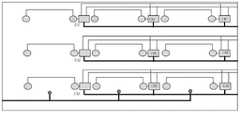
优选地,所述组合电容中控制层的N个开关中的每个开关的控制器都分别连接到控制总线上,连接到控制总线上的N个开关中的每个开关都被分配有一个地址,总线控制协议通过地址来具体识别每个开关,由外部或内部处理器通过地址来实现对每个开关的通、断进行控制;所述控制总线通过相应的导线连接到电容封装外部相应的总线控制引脚,所述导线与上电极C1、活动电极B1、下电极A1不重叠,并由外部处理器根据每个开关的地址来控制N个开关的通断,实现调整组合电容的步进调整,以及对组合电容容值的任意调整;其中内部处理器与外部处理器通过总线连接,传递所需电容的容值大小。Preferably, the controller of each of the N switches of the control layer in the combined capacitor is respectively connected to the control bus, and each switch of the N switches connected to the control bus is assigned an address , the bus control protocol specifically identifies each switch through the address, and the external or internal processor controls the on and off of each switch through the address; the control bus is connected to the corresponding bus outside the capacitor package through the corresponding wire Control pins, the wires do not overlap with the upper electrode C1, the movable electrode B1, and the lower electrode A1, and the external processor controls the on-off of the N switches according to the address of each switch, so as to realize the step adjustment of adjusting the combined capacitance , and any adjustment to the capacitance value of the combined capacitor; the internal processor and the external processor are connected through the bus, and the capacitance value of the required capacitor is transmitted.
优选地,所述组合电容中N个可调单元电容的使用模式为:初次使用或重置使用时的工作模式为,顺序通过控制器控制开关矩阵使每个可调单元电容的调整电极 C2加可调电压或不加可调电压,而每个下电极A1不加工作电压或加工作电压,从而使组合电容中的N个可调单元电容的容值为最小或最大值,完成初次或重置;Preferably, the use mode of the N adjustable unit capacitors in the combined capacitor is: the working mode during initial use or reset use is, the controller controls the switch matrix in sequence to make the adjustment electrode C2 of each adjustable unit capacitor increase. Adjustable voltage or no adjustable voltage is applied, and each lower electrode A1 is not applied with a working voltage or is applied with a working voltage, so that the capacitance value of the N adjustable unit capacitors in the combined capacitor is the minimum or maximum value, and the initial or repeated operation is completed. set;
在加电后组合电容容值最小时,给组合电容的所有下电极A1加上工作电压,通过调整控制器控制开关矩阵的开关通、断和调整或不调整可调电压大小实现组合电容的总容值的调整到期望的容值状态,同时保持控制开关矩阵的地址记忆并存储;When the capacitance value of the combined capacitor is the smallest after power-on, apply the working voltage to all the lower electrodes A1 of the combined capacitor, and adjust the switch on and off of the switch matrix by adjusting the controller to adjust or not adjust the adjustable voltage to realize the total value of the combined capacitor. The capacitance value is adjusted to the desired capacitance value state, while keeping the address memory and storage of the control switch matrix;
在加电后组合电容容值为最大时,通过控制组合电容的所有调整电极加调整电压,所有的下电极A1加上工作电压,调整控制开关矩阵的通、断和调整或不调整可调电压的大小,从而实现组合电容的总容值调整到期望的容值状态,同时保持此时控制开关地址的记忆并存储;When the combined capacitor capacitance value is the largest after power-on, the adjustment voltage is applied to all adjustment electrodes of the combined capacitor, and the working voltage is applied to all the lower electrodes A1 to adjust the on/off of the control switch matrix and adjust or not adjust the adjustable voltage The size of the combined capacitor can be adjusted to the desired capacitance value state, and at the same time, the memory and storage of the control switch address at this time can be maintained;
在组合电容已经调整到组合电容值期望容值时,再重新加电后,通过控制器的开关矩阵地址的记忆,将开关矩阵调整到组合电容期望容值的开关矩阵通断状态,再加下电极A1工作电压和调整电极的调整电压,则可以实现组合电容期望的容值,实现之后,组合电容的容值还可以通过控制器控制开关矩阵中相应的地址通、断,实现新的组合电容容值的调整;When the combined capacitor has been adjusted to the expected value of the combined capacitor, after re-powering on, the switch matrix is adjusted to the on-off state of the switch matrix with the desired value of the combined capacitor through the memory of the switch matrix address of the controller, and the following The working voltage of the electrode A1 and the adjustment voltage of the adjustment electrode can realize the desired capacitance value of the combined capacitor. After the realization, the capacitance value of the combined capacitor can also be turned on and off by the controller to control the corresponding address in the switch matrix to realize a new combined capacitor. adjustment of capacitance;
如果上述可调单元电容上电顺序和容值的调整变化及初始容值对使用电路有影响,需要考虑在应用本组合电容的电路中设计保护措施,比如将可调单元电容的容值调整到位后,再使应用电路处于工作状态。If the above-mentioned power-on sequence of the adjustable unit capacitor, the adjustment change of the capacitance value and the initial capacitance value have an impact on the circuit used, it is necessary to consider designing protective measures in the circuit applying this combined capacitor, such as adjusting the capacitance value of the adjustable unit capacitor in place. After that, make the application circuit work.
优选地,所述组合电容的封装外壳将N个可调电容封装在一个密封空间,组合电容的外部工作电压引脚、接地引脚、可调电压引脚和控制引脚分别通过引线、过孔连接到下电极A1、上电极C1、调整电极C2和控制开关实现对N个可调电容的封装。Preferably, the package casing of the combined capacitor encapsulates N adjustable capacitors in a sealed space, and the external working voltage pins, ground pins, adjustable voltage pins and control pins of the combined capacitors pass through leads and vias respectively. It is connected to the lower electrode A1, the upper electrode C1, the adjustment electrode C2 and the control switch to realize the encapsulation of N adjustable capacitors.
优选地,所述供电引脚、接地引脚和控制引脚表面均焊接有材料涂覆,所述封装外壳是非金属材料。Preferably, the surfaces of the power supply pins, the ground pins and the control pins are all welded with material coating, and the package shell is made of non-metallic materials.
优选地,所述组合电容中每个可调单元电容都可以单独可调,也可以多个可调单元电容进行任意组合调整,实现组合电容多种调节步进,具体实现方式是通过内部或外部处理器来控制控制层C4中的N个射频开关的通断实现对N个可调单元电容的容值的调整,从而实现对整个电容的容值调整。Preferably, each of the adjustable unit capacitors in the combined capacitor can be adjusted individually, or a plurality of adjustable unit capacitors can be adjusted in any combination to realize various adjustment steps of the combined capacitor. The processor controls the on-off of the N radio frequency switches in the control layer C4 to adjust the capacitance of the N adjustable unit capacitors, thereby realizing the adjustment of the capacitance of the entire capacitor.
本发明的有益效果:本发明提供的这种基于MEMS结构的可调电容,不仅具备高Q值,同时还具备高耐电压、耐电流的能力,而且通过多个单元电容封装在一个封装里面可以实现组合电容的容值连续、步进可调,电容的容值可以通过外部或者内部的处理器实现可编程可调,具备良好的应用环境适应性,且调节电极为可移动电极,且电位状态固定,避免了可变电容两端射频电路直流偏置对开关臂移动的影响;与常规可变电容不同的是,活动电极水平上下移动,电极本身无形变,可减少寄生电容且电容变化线性度更高;调节电极始终处于电场阻滞状态,减小了外来机械振动的影响;使用较低温度焊料将半导体与介质材料焊接,同时实现了圆片级封装。Beneficial effects of the present invention: The adjustable capacitor based on the MEMS structure provided by the present invention not only has a high Q value, but also has the ability to withstand high voltage and current, and can be packaged in one package through a plurality of unit capacitors. The capacitance value of the combined capacitor can be adjusted continuously and step by step. The capacitance value of the capacitor can be programmable and adjustable through an external or internal processor. It has good adaptability to the application environment, and the adjustment electrode is a movable electrode, and the potential state Fixed, avoiding the influence of the DC bias of the RF circuit at both ends of the variable capacitor on the movement of the switching arm; different from the conventional variable capacitor, the movable electrode moves up and down horizontally, and the electrode itself has no deformation, which can reduce the parasitic capacitance and the linearity of the capacitance change. Higher; the regulating electrode is always in the electric field block state, reducing the influence of external mechanical vibration; using lower temperature solder to solder the semiconductor and the dielectric material, while realizing wafer level packaging.
以下将结合附图对本发明做进一步详细说明。The present invention will be further described in detail below with reference to the accompanying drawings.
附图说明Description of drawings
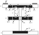
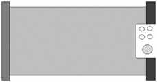
图1为本发明实施例一可调电容的构成整体剖面图。FIG. 1 is an overall cross-sectional view of the structure of an adjustable capacitor according to an embodiment of the present invention.
图2为本发明实施例一可调电容的下极板的结构图。FIG. 2 is a structural diagram of a lower electrode plate of an adjustable capacitor according to an embodiment of the present invention.
图3为本发明实施例一可调电容的活动极板的实施例结构图。FIG. 3 is a structural diagram of an embodiment of a movable electrode plate with adjustable capacitance according to an embodiment of the present invention.
图4为本发明实施例一可调电容的上极板极的实施例结构图。FIG. 4 is a structural diagram of an embodiment of an upper plate of an adjustable capacitor according to an embodiment of the present invention.
图5为本发明实施例一可调电容的上极板极的控制层实施例结构图。FIG. 5 is a structural diagram of an embodiment of a control layer of an upper plate of an adjustable capacitor according to an embodiment of the present invention.
图6为本发明实施例一可调电容的固定装置的结构图。FIG. 6 is a structural diagram of a fixing device for an adjustable capacitor according to an embodiment of the present invention.
图7为本发明实施例一可调电容的连接线导体的结构图。FIG. 7 is a structural diagram of a connecting wire conductor of an adjustable capacitor according to an embodiment of the present invention.
图8为本发明实施例一可调电容的封装的结构图。FIG. 8 is a structural diagram of a package of an adjustable capacitor according to an embodiment of the present invention.
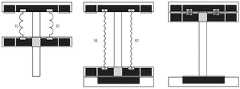
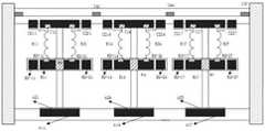
图9为本发明实施例二组合电容的横截面剖析结构图。FIG. 9 is a cross-sectional structural diagram of a combination capacitor according to a second embodiment of the present invention.
图10为本发明实施例二组合电容下极板结结构图。FIG. 10 is a structural diagram of the lower plate junction of the combined capacitor according to the second embodiment of the present invention.
图11为本发明实施例二组合电容的上极板结构图。FIG. 11 is a structural diagram of the upper plate of the combined capacitor according to the second embodiment of the present invention.
图12为本发明实施例二组合电容的上极板极的控制层结构图。FIG. 12 is a structural diagram of the control layer of the upper plate of the combined capacitor according to the second embodiment of the present invention.
图13为本发明实施例二可调单元电容的构成整体剖面图。FIG. 13 is an overall cross-sectional view of the structure of the adjustable unit capacitor according to the second embodiment of the present invention.
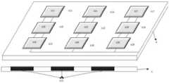
图14为本发明实施例二组合电容的封装的仰视图。FIG. 14 is a bottom view of the package of the combined capacitor according to the second embodiment of the present invention.
图15为本发明实施例二组合电容的连接线导体的结构图。FIG. 15 is a structural diagram of the connecting wire conductor of the combined capacitor according to the second embodiment of the present invention.
图16为本发明实施例二组合电容的封装俯视图。FIG. 16 is a top view of the package of the combined capacitor according to the second embodiment of the present invention.
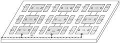
图17 为本发明实施例三组合电容的组合之二。FIG. 17 is the second combination of the three combination capacitors according to the embodiment of the present invention.
图18 为本发明实施例三组合电容的组合之三。FIG. 18 is the third combination of the three combination capacitors according to the embodiment of the present invention.
具体实施方式Detailed ways
为进一步阐述本发明达成预定目的所采取的技术手段及功效,以下结合附图及实施例对本发明的具体实施方式、结构特征及其功效,详细说明如下。In order to further illustrate the technical means and effects adopted by the present invention to achieve the predetermined purpose, the specific embodiments, structural features and effects of the present invention are described in detail below with reference to the accompanying drawings and examples.
下面将结合本发明实施例中的附图,对本发明实施例中的技术方案进行清楚、完整地描述,显然,所描述的实施例仅仅是本发明一部分实施例,而不是全部的实施例。基于本发明中的实施例,本领域普通技术人员在没有做出创造性劳动前提下所获得的所有其它实施例,都属于本发明保护的范围。The technical solutions in the embodiments of the present invention will be clearly and completely described below with reference to the accompanying drawings in the embodiments of the present invention. Obviously, the described embodiments are only a part of the embodiments of the present invention, but not all of the embodiments. Based on the embodiments of the present invention, all other embodiments obtained by those of ordinary skill in the art without creative efforts shall fall within the protection scope of the present invention.
在本发明的描述中,需要理解的是,术语“中心”、“上”、“下”、“前”、“后”、“左”、“右”、“垂直”、“水平”、“对齐”、“重叠”、“底”、“内”、“外”等指示的方位或位置关系为基于附图所示的方位或位置关系,仅是为了便于描述本发明和简化描述,而不是指示或暗示所指的装置或元件必须具有特定的方位、以特定的方位构造和操作,因此不能理解为对本发明的限制。In the description of the present invention, it should be understood that the terms "center", "upper", "lower", "front", "rear", "left", "right", "vertical", "horizontal", " The orientation or positional relationship indicated by "aligned", "overlapping", "bottom", "inner", "outer", etc. is based on the orientation or positional relationship shown in the drawings, and is only for the convenience of describing the present invention and simplifying the description, rather than An indication or implication that the referred device or element must have a particular orientation, be constructed and operate in a particular orientation, is not to be construed as a limitation of the invention.
术语“第一”、“第二”仅用于描述目的,而不能理解为指示或暗示相对重要性或者隐含指明所指示的技术特征的数量。由此,限定有“第一”、“第二”的特征可以明示或者隐含地包括一个或者更多个该特征;在本发明的描述中,除非另有说明,“多个”的含义是两个或两个以上。The terms "first" and "second" are only used for descriptive purposes, and should not be construed as indicating or implying relative importance or implicitly indicating the number of technical features indicated. Thus, the features defined with "first" and "second" may expressly or implicitly include one or more of the features; in the description of the present invention, unless otherwise specified, the meaning of "multiple" is two or more.
实施例1Example 1
本发明提供了一种基于MEMS结构的可调电容,包括下极板A,活动极板B、上极板C、固定装置D和连接线导体E,所述固定装置D的下端与下极板A固定垂直连接,固定装置D的上端与上极板C固定垂直连接,所述活动极板B的中部设置有开槽或通孔B4,活动极板B通过开槽或通孔B4设置于固定装置D中部,并且活动极板 B在固定装置D上进行上下移动;所述下极板A上设置有下电极A1,所述活动极板B 上设置有活动电极B1,调整电极B2;所述下电极A1与活动电极B1组成单元电容,该可单元电容为平行板电容;所述上极板C上设置有上电极C1、调整电极C2;所述连接线导体E两端分别与上电极C1、活动电极B1电连接;所述调整电极C2与调整电极B2组成调整单元。The present invention provides an adjustable capacitor based on a MEMS structure, comprising a lower electrode plate A, a movable electrode plate B, an upper electrode plate C, a fixing device D and a connecting wire conductor E, the lower end of the fixing device D being connected to the lower electrode plate A is fixed and vertically connected, the upper end of the fixing device D is fixed and vertically connected with the upper plate C, the middle part of the movable pole plate B is provided with a slot or a through hole B4, and the movable pole plate B is arranged in the fixed position through the slot or through hole B4 In the middle of the device D, and the movable electrode plate B moves up and down on the fixing device D; the lower electrode plate A is provided with a lower electrode A1, the movable electrode plate B is provided with a movable electrode B1, and an adjustment electrode B2; the The lower electrode A1 and the movable electrode B1 form a unit capacitor, and the unit capacitor is a parallel plate capacitor; the upper electrode C1 and the adjustment electrode C2 are provided on the upper electrode plate C; the two ends of the connecting wire conductor E are respectively connected to the upper electrode C1 , The movable electrode B1 is electrically connected; the adjustment electrode C2 and the adjustment electrode B2 form an adjustment unit.
所述连接线导体E包括连接线导体E1、连接线导体E2;所述活动电极B1的上表面设置有槽B3-1、槽B3-2,所述上电极C1的下表面设置有槽C1-1、槽C1-2;所述连接线导体E1的一端与上电极C1上的槽C1-1电连接,连接线导体E1的另一端与活动电极B1上的槽B3-1电连接;所述连接线导体E2的一端与上电极C1上的槽 C1-2电连接,连接线导体E2的另一端与活动电极B1上的槽B3-2电连接;这样,活动电极B1与上电极C1保持电性连接,活动电极B1与上电极C1之间的电路处于连通状态。The connecting wire conductor E includes a connecting wire conductor E1 and a connecting wire conductor E2; the upper surface of the movable electrode B1 is provided with a groove B3-1 and a groove B3-2, and the lower surface of the upper electrode C1 is provided with a groove C1- 1. Slot C1-2; one end of the connecting wire conductor E1 is electrically connected to the slot C1-1 on the upper electrode C1, and the other end of the connecting wire conductor E1 is electrically connected to the slot B3-1 on the movable electrode B1; the One end of the connecting wire conductor E2 is electrically connected to the slot C1-2 on the upper electrode C1, and the other end of the connecting wire conductor E2 is electrically connected to the slot B3-2 on the movable electrode B1; in this way, the movable electrode B1 and the upper electrode C1 remain electrically connected The circuit between the active electrode B1 and the upper electrode C1 is in a connected state.
所述调整电极B2包括调整电极B2-1、调整电极B2-2,所述调整电极C2包括调整电极C2-1、调整电极C2-2;所述调整电极C2-1与调整电极B2-1相对设置,所述调整电极C2-2与调整电极B2-2相对设置。The adjustment electrode B2 includes an adjustment electrode B2-1 and an adjustment electrode B2-2, and the adjustment electrode C2 includes an adjustment electrode C2-1 and an adjustment electrode C2-2; the adjustment electrode C2-1 is opposite to the adjustment electrode B2-1 The adjustment electrode C2-2 is arranged opposite to the adjustment electrode B2-2.
所述上极板C的上表面设置有控制层C4,所述控制层C4包括连接引线C4-2、连接引线C4-3、开关C4-1;所述连接引线C4-2将上电极C1连接至单元电容封装的接地引脚,所述连接引线C4-3将调整电极C2-1和调整电极C2-2连接起来,然后连接到开关C4-1的一端,开关C4-1的另一端连接到单元电容的可调电压引脚。The upper surface of the upper plate C is provided with a control layer C4, and the control layer C4 includes a connecting lead C4-2, a connecting lead C4-3, and a switch C4-1; the connecting lead C4-2 connects the upper electrode C1 To the ground pin of the unit capacitor package, the connecting lead C4-3 connects the adjustment electrode C2-1 and the adjustment electrode C2-2, and then connects to one end of the switch C4-1, and the other end of the switch C4-1 is connected to the Adjustable voltage pin for cell capacitor.
所述下电极A1的上表面设置有介质隔离层A2。A dielectric isolation layer A2 is provided on the upper surface of the lower electrode A1.
所述调整电极C2的下表面设置有介质隔离层C3。A dielectric isolation layer C3 is provided on the lower surface of the adjustment electrode C2.
具体的说,所述固定装置D的一端固定在下极板A的电极层的下电极A1的中心位置,且与下电极A1保持垂直,固定装置D的另一端固定在上极板的电极层的上电极C1的中心位置,且与上电极C1保持垂直,由固定装置D来固定、支撑上极板C 和下极板A,并使上极板C和下极板A之间保持平行、并相隔一定的间距,活动极板 B在静电力的作用下可以在上极板C和下极板A之间上下移动,由活动极板B移动导致活动电极B1和下电极A1之间的距离产生变化,从而改变单元电容的大小,所述调整电极C2与调整电极B2组成调整单元,调整电极C2位于上电极C1的外围且与上电极C1之间通过介质材料隔离,调整电极C2与活动电极B1、下电极A1不重叠,调整电极C2与活动极板B的调整电极B2由介质覆盖层C3进行隔离;调整电极B2 位于活动电极B1的外围,调整电极B2与活动电极B1之间通过介质材料隔离,调整电极B2与上电极C1、下电极A1都不重叠,下电极A1、活动电极B1、调整电极B2 和上电极C1、调整电极C2都为金属构成。Specifically, one end of the fixing device D is fixed at the center of the lower electrode A1 of the electrode layer of the lower electrode plate A, and is kept perpendicular to the lower electrode A1, and the other end of the fixing device D is fixed at the center of the electrode layer of the upper electrode plate A. The center position of the upper electrode C1 is kept perpendicular to the upper electrode C1, and the upper electrode plate C and the lower electrode plate A are fixed and supported by the fixing device D, and the upper electrode plate C and the lower electrode plate A are kept parallel and parallel. At a certain distance, the movable electrode B can move up and down between the upper electrode C and the lower electrode A under the action of electrostatic force, and the distance between the movable electrode B1 and the lower electrode A1 is caused by the movement of the movable electrode B. The adjustment electrode C2 and the adjustment electrode B2 form an adjustment unit, the adjustment electrode C2 is located on the periphery of the upper electrode C1 and is separated from the upper electrode C1 by a dielectric material, and the adjustment electrode C2 and the movable electrode B1 , The lower electrode A1 does not overlap, the adjustment electrode C2 and the adjustment electrode B2 of the movable electrode plate B are separated by the dielectric cover layer C3; the adjustment electrode B2 is located on the periphery of the movable electrode B1, and the adjustment electrode B2 and the movable electrode B1 are separated by a dielectric material The adjustment electrode B2 does not overlap with the upper electrode C1 and the lower electrode A1, and the lower electrode A1, the movable electrode B1, the adjustment electrode B2 and the upper electrode C1 and the adjustment electrode C2 are all made of metal.
所述下极板A,活动极板B、上极板C均是由单晶硅制成。The lower electrode plate A, the movable electrode plate B and the upper electrode plate C are all made of single crystal silicon.
本实施例中的可调电容的容值具体与下电极A1、活动电极B1的面积,下电极 A1上覆盖的介质隔离层A2的层数、厚度以及介质隔离层A2的介电常数,下电极A1 和活动电极B1之间的间距决定,具体的计算过程如下:The capacitance value of the adjustable capacitor in this embodiment is specifically related to the area of the lower electrode A1 and the movable electrode B1, the number and thickness of the dielectric isolation layer A2 covered on the lower electrode A1, and the dielectric constant of the dielectric isolation layer A2, and the lower electrode The distance between A1 and the active electrode B1 is determined. The specific calculation process is as follows:
本实施例中下电极A1上覆盖的介质隔离层A2在本实施例中为单层,也可以为多层,介质隔离层A2的厚度为d1,介电常数为ε1,活动电极B1和下电极A1间的空气距离为d2,空气介电常数分别是ε2,两者的电容分别是C1、C2,在本实施例中活动电极B1和下电极A1的面积都是S,按照该平行板电容的计算公式,其中:In this embodiment, the dielectric isolation layer A2 covered on the lower electrode A1 is a single layer in this embodiment, and may also be a multi-layer. The thickness of the dielectric isolation layer A2 is d1 , the dielectric constant is ε1 , and the active electrodes B1 and The air distance between the lower electrodes A1 is d2 , the dielectric constants of the air are ε2 respectively, and the capacitances of the two are C1 and C2 , respectively. In this embodiment, the areas of the movable electrode B1 and the lower electrode A1 are both S, According to the calculation formula of the parallel plate capacitance, where:


则本实施例中,可调单元电容C为C1和C2的串联值之和为:In this embodiment, the adjustable unit capacitance C is the sum of the series values of C1 and C2:

其中d2为活动电极B1和下电极A1之间的间距,可以通过调整静电力来调整d2 的值,具体d2的调整方法如下:Among them, d2 is the distance between the movable electrode B1 and the lower electrode A1. The value of d2 can be adjusted by adjusting the electrostatic force. The specific adjustment method of d2 is as follows:
本实施例中假设下极板A上的电极层下电极A1加工作电压V后对活动极板B上的活动电极B1产生的静电力为Fx,上极板C上的电极层调整电极C2加可调电压V1 后对活动极板B上调整电极B2产生的静电力为Fs,活动极板B的自重力为Fg,活动极板B在固定装置D上移动时与固定装置D之间的摩擦力为Fz,连接线导体E1和连接线导体E2的拉力的合力在整个拉伸过程中都是均匀的且拉力值为Fl,连接线导体E1和连接线导体E2的弹力在连接线导体整个被压缩过程中都是均匀的且弹力的值都为Ft,当Fs>Fx+Fg+Fz+Ft时,活动极板B受向上的静电力拉向并贴近上极板C,此时d2的取值最大,由公式3可以知道,其它参数不变,当d2取值最大时,可调单元电容的容值C最小;当Fx+Fg>Fs+Fl+Fz时,活动极板受向下的静电拉力移向并贴近下极板,此时d2的取值最小,由公式3可以知道,其它参数不变,当d2取值最小时,可调单元电容的容值C最大;当Fs+Fl=Fx+Fg+Ft时,活动极板B处于上、下极板之间某个不确定的位置,此时可调单元电容的容值处于中间不确定值,为避免可调电容的容值处于不确定状态,因此要通过控制可调电压的电压值来避免出现 Fs+Fl=Fx+Fg+Ft这种状态,从而避免可调单元电容的容值处于不确定状态。In this embodiment, it is assumed that the electrostatic force generated on the movable electrode B1 on the movable electrode plate B after the lower electrode A1 of the electrode layer on the lower electrode plate A is applied with the working voltage V is Fx, and the electrode layer adjustment electrode C2 on the upper electrode plate C is applied to the movable electrode B1. After adjusting the voltage V1, the electrostatic force generated by the adjustment electrode B2 on the movable electrode plate B is Fs, the self-gravity of the movable electrode plate B is Fg, and the friction between the movable electrode plate B and the fixing device D when the movable electrode B moves on the fixing device D The force is Fz, the resultant force of the pulling force of the connecting wire conductor E1 and the connecting wire conductor E2 is uniform in the whole stretching process, and the pulling force value is F1, and the elastic force of the connecting wire conductor E1 and the connecting wire conductor E2 is in the entire connecting wire conductor. The compression process is uniform and the value of the elastic force is Ft. When Fs>Fx+Fg+Fz+Ft, the movable plate B is pulled by the upward electrostatic force and is close to the upper plate C. At this time, the value of d2 is It can be known from formula 3 that other parameters remain unchanged. When the value of d2 is the largest, the capacitance value C of the adjustable unit capacitor is the smallest; when Fx+Fg>Fs+Fl+Fz, the movable plate is subjected to downward The electrostatic pulling force moves to and close to the lower plate, and the value of d2 is the smallest at this time. It can be known from formula 3 that other parameters remain unchanged. When the value of d2 is the smallest, the capacitance value C of the adjustable unit capacitor is the largest; when Fs+Fl =Fx+Fg+Ft, the movable plate B is in an uncertain position between the upper and lower plates, and the capacitance value of the adjustable unit capacitor is in the middle uncertain value. In order to avoid the capacitance value of the adjustable capacitor It is in an uncertain state, so it is necessary to control the voltage value of the adjustable voltage to avoid the state of Fs+Fl=Fx+Fg+Ft, so as to prevent the capacitance value of the adjustable unit capacitor from being in an uncertain state.
另外本实施例中的可调电容在受到外界机械扰动或振动条件下,d2会因振动产生微小变化,假设变化量为Δd2,相应地总电容C的变化量是ΔC,根据上式3把d2作为自变量的关于C的函数,C=f(d2),求微分可得:In addition, when the adjustable capacitor in this embodiment is subjected to external mechanical disturbance or vibration, d2 will change slightly due to vibration. Assuming that the change is Δd2 , the corresponding change of the total capacitance C is ΔC. According to the above formula 3 d2 is a function of C as an independent variable, C=f(d2 ), and the differentiation can be obtained:

则可计算得出总电容变化的百分比是:The percent change in total capacitance can then be calculated as:

根据上式,可得出结论

本实施例中,所述可调电容的Q值的计算公式如下:Q=1/wCR,其中R为电容的等效电阻值,该值主要由下电极A1到电容引脚电阻R1,下电极阻值R2,活动电极 B1的阻值R3,上电极C1的电阻值R4,连接线导体E1和连接线导体E2的阻值之和 R5,R=R1+R2+R3+R4+R5,要保证R的取值是最小的,则要,尽量保证各部分的阻值都取最小值,此时本实施例中可调单元电容的Q值才能取值为最小。In this embodiment, the calculation formula of the Q value of the adjustable capacitor is as follows: Q=1/wCR, where R is the equivalent resistance value of the capacitor, which is mainly from the lower electrode A1 to the capacitor pin resistance R1, and the lower electrode The resistance value R2, the resistance value R3 of the movable electrode B1, the resistance value R4 of the upper electrode C1, the sum of the resistance values of the connecting wire conductor E1 and the connecting wire conductor E2 R5, R=R1+R2+R3+R4+R5, it is necessary to ensure If the value of R is the smallest, it is necessary to try to ensure that the resistance values of each part take the smallest value. At this time, the Q value of the adjustable unit capacitor in this embodiment can take the smallest value.
所述本实施例中,上电极C1、活动电极B1、下电极A1的形状和尺寸完全相同为长方形,所述的上极板C上的调整电极C2,活动极板B上调整电极B2,由调整电极C2-1、调整电极C2-2,以及调整电极B2-1、调整电极B2-2组成,且调整电极C2-1 和调整电极C2-2对称分布在上电极C1两边,调整电极B2-1和调整电极B2-2对称分布在活动电极B1两边,调整电极C2-1和调整电极B2-1在垂直方向上重叠,调整电极C2-2和调整电极B2-2在垂直方向上重叠,固定装置D的一端固定在上电极C1 的中心位置,固定装置D的另一端固定在下电极A1的中心位置,活动极板B上中心位置有开槽或通孔B4,开槽或通孔B4的形状与固定装置D的横截面形状相同,尺寸略大,两个连接线导体E1和连接线导体E2的固定点处于活动极板的中心平衡线上,在连接线导体E1和连接线导体E2自然悬挂状态下,活动极板B能够自然平行于上极板C、下极板A,以上尺寸和外观的设计,确保了调整电极C2-1和调整电极C2-2 加电后对调整电极B2-1和调整电极B2-2的静电吸引力均匀对称,下电极A1加电后对活动电极B1产生的静电力均匀对称,从而保证活动极板B在上极板C和下极板A 之间上下移动时能够稳定移动,活动极板B和固定装置D之间产生的摩擦力最小。In the present embodiment, the shape and size of the upper electrode C1, the movable electrode B1 and the lower electrode A1 are exactly the same as rectangles, and the adjustment electrode C2 on the upper electrode plate C and the adjustment electrode B2 on the movable electrode plate B are composed of Adjustment electrode C2-1, adjustment electrode C2-2, adjustment electrode B2-1, adjustment electrode B2-2 are composed, and adjustment electrode C2-1 and adjustment electrode C2-2 are symmetrically distributed on both sides of upper electrode C1, adjustment electrode B2- 1 and the adjustment electrode B2-2 are symmetrically distributed on both sides of the movable electrode B1, the adjustment electrode C2-1 and the adjustment electrode B2-1 overlap in the vertical direction, the adjustment electrode C2-2 and the adjustment electrode B2-2 overlap in the vertical direction, fixed One end of the device D is fixed at the center position of the upper electrode C1, the other end of the fixing device D is fixed at the center position of the lower electrode A1, and there is a slot or through hole B4 in the center position of the movable plate B, and the shape of the slot or through hole B4 The cross-sectional shape is the same as that of the fixing device D, but the size is slightly larger. The fixing points of the two connecting wire conductors E1 and E2 are on the center balance line of the movable plate, and the connecting wire conductors E1 and E2 are naturally suspended. In the state, the movable electrode plate B can be naturally parallel to the upper electrode plate C and the lower electrode plate A. The above size and appearance design ensures that the adjustment electrode C2-1 and the adjustment electrode C2-2 can be adjusted to the adjustment electrode B2-1 after power-on. It is uniform and symmetrical with the electrostatic attraction force of the adjusting electrode B2-2, and the electrostatic force generated by the lower electrode A1 to the movable electrode B1 after electrification is uniform and symmetrical, thereby ensuring that the movable electrode B moves up and down between the upper electrode C and the lower electrode A. It can move stably, and the friction force between the movable plate B and the fixed device D is the smallest.
图2为本实施例中可调电容的下极板A的结构斜视图和剖面图,本实施例中下极板A的实现工艺是先通过在单晶硅上形成下极板A的基板,在形成电容区域刻蚀浅槽,溅射金属形成可调电容下电极A1,再在可调电容下电极A1上沉淀介质材料形成介质隔离层A2,该介质材料沉淀的层数,可以根据需要实现的电容的容值和Q值来选择,本实施例中沉淀的介质材料为一层,也可以为多层,沉淀介质隔离层A2的表面为平滑表面,以便活动电极B1与下电极A1接近时,介质隔离层A2和活动电极 B1能够紧密接触,从而增强电容在此状态下的防震动能力,同时介质材料层A2的厚度值的选择还要参考可调电容的工作频段,使可调电容的谐振频率和电容的工作频率不同频,从而避免产生谐振,在下电极A1同时加射频信号和直流型号时,震荡信号的幅度相等、相位相反互相抵消或防止加射频信号后产生的谐振,同时下电极A1 金属导体阻值还影响可调电容的Q值,其电阻值越小,可调电容的Q值就越大,同时下电极A1和上面覆盖的介质材料A2的阻值、尺寸还影响可调电容的下电极的耐压和耐流能力2 is a perspective view and a cross-sectional view of the structure of the lower electrode plate A of the adjustable capacitor in this embodiment. The realization process of the lower electrode plate A in this embodiment is to first form the substrate of the lower electrode plate A on monocrystalline silicon, In the area where the capacitor is formed, a shallow groove is etched, metal is sputtered to form the lower electrode A1 of the adjustable capacitance, and then a dielectric material is deposited on the lower electrode A1 of the adjustable capacitance to form the dielectric isolation layer A2. The number of layers of the deposited dielectric material can be realized as required. The capacitance and Q value of the capacitor are selected according to the capacitance value and Q value of the capacitor. In this embodiment, the deposited dielectric material is one layer or multiple layers. The surface of the deposited dielectric isolation layer A2 is a smooth surface, so that when the movable electrode B1 is close to the lower electrode A1 , the dielectric isolation layer A2 and the movable electrode B1 can be in close contact, thereby enhancing the anti-vibration capability of the capacitor in this state. At the same time, the selection of the thickness value of the dielectric material layer A2 should refer to the working frequency band of the adjustable capacitor, so that the The resonance frequency is different from the working frequency of the capacitor, so as to avoid resonance. When the RF signal and the DC model are applied to the lower electrode A1 at the same time, the amplitude of the oscillating signal is equal and the phase is opposite to each other to cancel each other or prevent the resonance generated by adding the RF signal. The resistance value of the metal conductor of A1 also affects the Q value of the adjustable capacitor. The smaller the resistance value, the greater the Q value of the adjustable capacitor. At the same time, the resistance value and size of the lower electrode A1 and the dielectric material A2 covered on it also affect the adjustable capacitor. The voltage and current withstand capability of the lower electrode of the capacitor
图3为本实施例中可调电容活动极板B的结构斜视图和横截面图,本实施例中其实现工艺是以单晶硅为基板制作活动极板B,在活动电极区和调整电极区分别刻蚀浅槽,溅射金属并平坦化,将槽内填满金属分别形成活动电极B1和调整电极B2,其中活动电极B1的面积和形状与下电极A1的面积和形状完全一致,以保证下电极A1 加电后对活动电极B1的静电力在活动电极的各个受力点均匀对称分布,调整电极 B2-1和调整电极B2-2的面积和形状与调整电极C2-1和调整电极C2-2的面积和形状完全一致,以确保调整电极C2加电后对调整电极B2各个受力点均匀对称分布,再把活动板B中央刻蚀掉与固定装置截面形状相同的开槽或通孔B4,与固定装置D配合实现上下稳定移动,开槽或通孔B4的两边对称的活动极板B的纵向中轴线上固定连接线导体的地方设置槽B3-1和槽B3-2,开槽深度要能够确保连接线导体E1和连接线导体E2被压缩后能够隐藏至少50%在活动极板的槽B3-1和槽B3-2内部,并将连接线导体E1和连接线导体E2的一端分别固定在槽B3-1和槽B3-2内,使E1和E2 分别与活动电极在电路上互通。3 is a perspective view and a cross-sectional view of the structure of the adjustable capacitor movable electrode plate B in this embodiment. In this embodiment, the realization process is to use monocrystalline silicon as the substrate to make the movable electrode plate B. In the movable electrode area and the adjustment electrode Etching shallow grooves, sputtering metal and planarizing, filling the grooves with metal to form active electrodes B1 and adjustment electrodes B2, wherein the area and shape of the active electrode B1 are exactly the same as the area and shape of the lower electrode A1, so that Ensure that the electrostatic force on the movable electrode B1 after the lower electrode A1 is energized is evenly and symmetrically distributed at each force point of the movable electrode, and the area and shape of the adjustment electrode B2-1 and the adjustment electrode B2-2 are adjusted to the adjustment electrode C2-1 and the adjustment electrode. The area and shape of C2-2 are exactly the same to ensure that the force points of the adjusting electrode B2 are evenly and symmetrically distributed after the adjusting electrode C2 is powered on, and then the center of the movable plate B is etched away with the same shape as the fixed device. Hole B4, cooperates with fixing device D to realize stable movement up and down, slot B3-1 and slot B3-2 are set on the longitudinal center axis of movable pole plate B symmetrical on both sides of slot or through hole B4, and slot B3-1 and slot B3-2 are set. The depth of the slot should be able to ensure that the connecting wire conductor E1 and the connecting wire conductor E2 can be hidden at least 50% inside the slots B3-1 and B3-2 of the movable plate after being compressed, and the connecting wire conductor E1 and the connecting wire conductor E2 can be hidden. One end is respectively fixed in the slot B3-1 and the slot B3-2, so that E1 and E2 respectively communicate with the movable electrode on the circuit.
图4本实施例中可调电容上极板C的结构斜视图和横截面图,本实施例中其实现工艺是以单晶硅为基板制作上极板C,在上电极区域及其两侧的调整电极区域刻蚀浅槽,形成浅槽后在可调电极区域的中央继续钻孔刻蚀出深槽,然后溅射金属并平坦化,将槽内填满金属,上层浅槽的金属形成可调电容上电极C1和调整电极C2-1、调整电极C2-2,调整电极C2-1、调整电极C2-2和调整电极B2-1、调整电极B2-2位置相对、形状接近,以使调整电极C2加可调电压后对活动电极B2各个受力点的静电吸引力是均匀对称分布的,再在调整电极C2-1和调整电极C2-2的表面沉淀介质形成介质保护层C3-1和介质保护层C3-2,保护介质层C3的表面光滑,用于隔离调整电极C2和活调整电极B2,在上电极C1的横向中轴线上两边对称的和活动极板调整电极类似对应的位置,分别通过刻蚀设置槽C1-1和槽C1-2,槽深度长、宽尺寸要能够满足连接线导体E1和连接线导体E2被压缩时能够在开槽内被隐藏50%以上,再将连接线导体E1和连接线导体E2的另一端分别固定在槽C1-1和槽C1-2内部,使连接线导体E和上电极C1之间电路上保持连通。FIG. 4 is an oblique view and a cross-sectional view of the structure of the upper electrode plate C of the adjustable capacitor in this embodiment. In this embodiment, the realization process is to use monocrystalline silicon as the substrate to make the upper electrode plate C. In the upper electrode area and its two sides The adjustment electrode area is etched with a shallow groove. After forming a shallow groove, continue to drill and etch a deep groove in the center of the adjustable electrode area, then sputter metal and flatten it, fill the groove with metal, and form the metal of the upper shallow groove. Adjustable capacitor upper electrode C1, adjustment electrode C2-1, adjustment electrode C2-2, adjustment electrode C2-1, adjustment electrode C2-2, adjustment electrode B2-1, adjustment electrode B2-2 are opposite in position and close in shape, so that the After the adjustment electrode C2 is applied with an adjustable voltage, the electrostatic attraction to each force point of the movable electrode B2 is evenly and symmetrically distributed, and then the medium is deposited on the surface of the adjustment electrode C2-1 and the adjustment electrode C2-2 to form a dielectric protective layer C3-1 And the dielectric protective layer C3-2, the surface of the protective dielectric layer C3 is smooth, used to isolate the adjustment electrode C2 and the active adjustment electrode B2, on the lateral center axis of the upper electrode C1, the two sides are symmetrical and the movable plate adjustment electrode is similar to the corresponding position , set the groove C1-1 and the groove C1-2 by etching, respectively. The length and width of the groove should be able to meet the requirements that the connecting wire conductor E1 and the connecting wire conductor E2 can be hidden in the slot by more than 50% when they are compressed. The other ends of the connecting wire conductor E1 and the connecting wire conductor E2 are respectively fixed inside the slot C1-1 and the slot C1-2, so that the electrical connection between the connecting wire conductor E and the upper electrode C1 is maintained.
图5本实施例中可调电容上极板的控制层剖面图,在上极板C的上表层为控制层C4,控制层C4主要分布用连接引线C4-2、连接引线C4-3和开关C4-1,其中连接引线C4-2主要是将上电极C1连接至电容封装的接地引脚,引线导体C4-3的功能是将调整电极C2-1和调整电极C2-2连接起来然后连接到开关C4-1,开关C4-1的另一端连接到可调电容的可调电压引脚,同时开关C4-1的数据收发控制总线通过引出线连接到电容控制引脚。Figure 5 is a cross-sectional view of the control layer of the upper plate of the adjustable capacitor in this embodiment, the upper surface layer of the upper plate C is a control layer C4, and the control layer C4 is mainly distributed with connecting leads C4-2, connecting leads C4-3 and switches C4-1, the connecting lead C4-2 is mainly to connect the upper electrode C1 to the ground pin of the capacitor package, and the function of the lead conductor C4-3 is to connect the adjustment electrode C2-1 and the adjustment electrode C2-2 and then connect to The switch C4-1, the other end of the switch C4-1 is connected to the adjustable voltage pin of the adjustable capacitor, and the data transceiver control bus of the switch C4-1 is connected to the capacitor control pin through the lead wire.
图6为本实施例中可调电容固定装置D的实施例结构图,其具体实现工艺是,可以通过淀积或键合的方式实现固定装置D,将固定装置D的一端固定在下极板A的下电极A1中心,且与下极板A垂直,固定装置D的另一端固定在可调电容的上极板 C的上电极C1的中心位置,且与上极板C垂直,固定装置D在上极板C、下极板A 之间支撑上极板C和下极板A,并保持上极板C、下极板A平行,固定装置D的固定形式包括但不限于固定轴、固定板、固定腔体、固定弹簧等形式。6 is a structural diagram of an embodiment of the adjustable capacitor fixing device D in this embodiment. The specific implementation process is that the fixing device D can be realized by means of deposition or bonding, and one end of the fixing device D is fixed on the lower plate A. The center of the lower electrode A1 is perpendicular to the lower electrode plate A, and the other end of the fixing device D is fixed at the center position of the upper electrode C1 of the upper electrode plate C of the adjustable capacitor, and is perpendicular to the upper electrode plate C, and the fixing device D is at The upper pole plate C and the lower pole plate A are supported between the upper pole plate C and the lower pole plate A, and the upper pole plate C and the lower pole plate A are kept parallel. The fixed form of the fixing device D includes but is not limited to a fixed shaft, a fixed plate , fixed cavity, fixed spring and other forms.
图7为本实施例中可调电容连接线导体E的实施例结构图,所述的连接线导体 E1和连接线导体E2由具备伸、缩性能的金属导体构成,连接线导体E1的一端固定在槽B3-1内,连接线导体E1另一端固定在槽C1-1内,连接线导体E2的一端固定在槽B3-2内,连接线导体E2的另一端固定在槽C1-2内,从结构图中可以看出连接线导体E1和连接线导体E2有三种典型的状态,分别是第一种状态为连接线导体E1 和连接线导体E2被拉伸到了最长的状态,此时活动电极B1受的下极板下电极A1加上工作电压后,且工作电压产生的静电力加活动极板的自重力大于活动极板的摩擦力、向上的拉伸力、上极板调整电极C2-1、C2-2对活动极板的静电吸引力之和后活动极板B和下极板A紧密接触;第二种状态为连接线导体E1和连接线导体E2被压缩到了最短的状态,此时活动极板B的调整电极B2-1和调整电极B2-2受上极板C的调整电极C2-1和调整电极C2-2加上可调电压后产生的静电力大于活动极板的自重力、摩擦力、向下的弹力、下极板下电极A1对活动极板的静电力之和,此时由上极板调整电极C2-1和C2-2将活动极板B吸引到与上极板C紧密接触,在这种状态下,连接线导体E1和连接线导体E2被隐藏在槽B3-1、槽B3-2和槽C1-1、槽C1-2 内部;第三种状态为连接线导体E处于中间任意值状态,正常情况下电容工作过程中应该避免出现这种状态,因为该状态下可调电容的容值是不确定值,所选的连接线导体E1和槽E2有抗疲劳特性能够被反复拉伸和压缩,连接线导体都不会断,同时拉伸和压缩过程中连接线导体的拉伸力和压缩时的弹力始终保持为恒定值;为减少连接线导体的电阻值对可调电容的Q值的影响,所选连接线导体的材料为高导电率的材料。FIG. 7 is a structural diagram of an embodiment of the adjustable capacitance connecting wire conductor E in this embodiment. The connecting wire conductor E1 and the connecting wire conductor E2 are composed of metal conductors with stretching and shrinking properties, and one end of the connecting wire conductor E1 is fixed In the slot B3-1, the other end of the connecting wire conductor E1 is fixed in the slot C1-1, one end of the connecting wire conductor E2 is fixed in the slot B3-2, and the other end of the connecting wire conductor E2 is fixed in the slot C1-2, It can be seen from the structure diagram that the connecting line conductor E1 and the connecting line conductor E2 have three typical states, respectively, the first state is that the connecting line conductor E1 and the connecting line conductor E2 are stretched to the longest state, and the active state is After the lower electrode A1 of the lower electrode plate received by the electrode B1 is applied with the working voltage, and the electrostatic force generated by the working voltage plus the self-gravity of the movable electrode plate is greater than the friction force of the movable electrode plate, the upward tensile force, the upper electrode plate adjusts the electrode C2 -1. After the electrostatic attraction of C2-2 to the movable electrode plate, the movable electrode plate B and the lower electrode plate A are in close contact; the second state is that the connecting wire conductor E1 and the connecting wire conductor E2 are compressed to the shortest state, At this time, the adjustment electrode B2-1 and the adjustment electrode B2-2 of the movable plate B are subjected to the adjustment electrode C2-1 and the adjustment electrode C2-2 of the upper plate C, and the electrostatic force generated by the adjustable voltage is greater than that of the movable electrode plate. The sum of self-gravity, frictional force, downward elastic force, and the electrostatic force of the lower electrode A1 on the lower electrode plate to the movable electrode plate. At this time, the movable electrode plate B is attracted by the upper electrode plate adjustment electrodes C2-1 and C2-2 to the movable electrode plate B. The upper plate C is in close contact, and in this state, the connecting wire conductor E1 and the connecting wire conductor E2 are hidden in the slots B3-1, B3-2 and inside the slots C1-1 and C1-2; the third state Because the connection line conductor E is in the middle of any value state, this state should be avoided during the capacitor operation process under normal circumstances, because the capacitance value of the adjustable capacitor in this state is an uncertain value, the selected connection line conductor E1 and slot E2 It has anti-fatigue properties and can be repeatedly stretched and compressed, and the conductors of the connecting wires will not be broken. At the same time, the tensile force and elastic force of the connecting wire conductors during the stretching and compression process are always kept constant; in order to reduce the number of connecting wire conductors The influence of the resistance value on the Q value of the adjustable capacitor, the material of the selected connecting wire conductor is a material with high conductivity.
图8本实施例中可调电容封装的实施例结构图,单个可调电容溅射金属形成电容下电极A1,在下电极A1的基础上沉淀介质材料形成介质隔离层A2,淀积金属引线将电容下电极A1连接,引出到工作电压引脚,通过淀积或键合的方式,在介质材料贵A2的中兴位置制作固定装置D,固定装置的形式包括但不限于固定轴、固定板、固定腔体、固定弹簧等形式,固定装置D使活动板B在上极板C、下极板A之间上下稳定移动,且在水平方向上不偏移,移动时不卡顿、不增加阻力。Fig. 8 is a structural diagram of an embodiment of the adjustable capacitor package in this embodiment. A single adjustable capacitor is sputtered metal to form a capacitor lower electrode A1, a dielectric material is deposited on the basis of the lower electrode A1 to form a dielectric isolation layer A2, and metal leads are deposited to separate the capacitor The lower electrode A1 is connected to the working voltage pin, and the fixing device D is made at the ZTE position of the dielectric material A2 by means of deposition or bonding. The form of the fixing device includes but is not limited to a fixed shaft, a fixed plate, and a fixed cavity. The fixing device D enables the movable plate B to move stably up and down between the upper pole plate C and the lower pole plate A, and does not shift in the horizontal direction, and does not get stuck or increase resistance when moving.
以单晶硅为基板制作活动极板B,在活动电极B1区和调整电极B2区分别刻蚀浅槽,溅射金属并平坦化,将槽内填满金属,形成活动电极B1和调整电极B2,在在活动极板上设置槽B3-1和槽B3-2,再把活动板中央刻蚀掉与固定装置截面形状相同的开槽或通孔B4,然后将活动极板上的开槽或通孔B4穿过固定装置D,活动电极B1 那一面朝下,调整电极B2面朝上,然后在槽B3-1和槽B3-2上分别固定连接线导体 E1和连接线导体E2的一端。Use monocrystalline silicon as the substrate to make the movable electrode plate B, etch shallow grooves in the movable electrode B1 area and the adjustment electrode B2 area, sputter metal and flatten it, and fill the groove with metal to form the movable electrode B1 and the adjustment electrode B2 , set slot B3-1 and slot B3-2 on the movable pole plate, then etch the slot or through hole B4 with the same cross-sectional shape as the fixed device in the center of the movable plate, and then etch the slot or through hole B4 on the movable pole plate. The through hole B4 passes through the fixing device D, the side of the movable electrode B1 is facing down, and the side of the adjusting electrode B2 is facing up, and then one end of the connecting wire conductor E1 and the connecting wire conductor E2 are respectively fixed on the slot B3-1 and the slot B3-2. .
以单晶硅为基板制作上极板C,在形成电容区域及其两侧的可调电极区域刻蚀浅槽,形成浅槽后在可调电极区域的中央继续钻孔刻蚀出深槽,然后溅射金属并平坦化,将槽内填满金属,上层浅槽的金属形成电容上电极C1和调整电极C2-1、调整电极C2-2,下部深槽填充金属形成引出导线,并与开关C4-1相连,淀积金属引线将上电极和调整电极引出到上极板边缘,上极板制作完成后,将上极板C与固定装置D 键合,使上极板C和下极板A电气装配在一起,再从封装两端,分别将上极板C上的控制层C4的上电极引出线、开关的控制引出线和可调电压引出线,从电容的两端侧面分别引出到电容的接地引脚、控制引脚和可调电压引脚上。The upper plate C is made with single crystal silicon as the substrate, and the shallow groove is etched in the area where the capacitor is formed and the adjustable electrode area on both sides. Then metal is sputtered and flattened, and the groove is filled with metal. The metal in the upper shallow groove forms the capacitor upper electrode C1, the adjustment electrode C2-1 and the adjustment electrode C2-2, and the lower deep groove is filled with metal to form the lead wire, which is connected with the switch. Connect to C4-1, deposit metal leads to lead the upper electrode and adjustment electrode to the edge of the upper electrode plate, after the upper electrode plate is fabricated, bond the upper electrode plate C with the fixing device D, so that the upper electrode plate C and the lower electrode plate are bonded together. A is electrically assembled together, and then from the two ends of the package, the upper electrode lead wire of the control layer C4 on the upper plate C, the control lead wire of the switch and the adjustable voltage lead wire are respectively led out from the two sides of the capacitor to the On the ground pin, control pin, and adjustable voltage pin of the capacitor.
实施例2Example 2
本实施例提供了一种如图9~图16所示的该组合电容由9个可调单元电容构成, 9个可调单元电容的上电极C11、C12、C13、C14、C15、C16、C17、C18、C19,以及 9对上极板调整电极C211、C221,C212、C222,C213、C223,C214、C224,C215、 C225,C216、C226,C217、C227,C218、C228,C219、C229共同分布在一个上极板上且相互之间相互隔离,其中C11、C12、C13在电极层相互连接为一组,C14、C15、 C16在电极层相互连接为一组,C17、C18、C19在电极层相互连接为一组,一共三组,然后每一组再分别连接到一个总引线导体上,再由总引线导体连接到电容的接地引脚,上极板9对调整电极中的每对调整电极都通过引线导体相互连接,然后每对调整电极再连接到开关矩阵中的一个开关的一端,该开关的另一端都通过引线导体连接到可调单元电容的可调电压引脚;组合电容中的9个下电极A11、A12、A13、A14、 A15、A16、A17、A18、A19共同分布在一个下极板上且相互之间相互隔离,然后A11、 A12、A13通过相互连接成一组,A14、A15、A16通过相互连接成一组,A17、A18、 A19通过相互连接成一组,共三组下电极再分别连接到一根引线导体,引线导体再连接到组合电容工作电压引脚;其中上极板电极层中的上电极与上电极引线之间,上电极和调整电极引线之间由介质相互绝缘隔离,下极板下电极之间的引线与引线之间隔离,引线与上极板电极层上电极、调整电极、下极板的下电极之间隔离或者不重叠;9个上电极和9个下电极之间有相同的外形尺寸,并且在垂直方向上严格对齐,对应的9个固定装置和9组连接线导体共同组成组合电容,下极板上的电极层的分布的9个下电极与可以在9个固定装置上移动的9个相对应的活动极板的活动电极组成9个单元电容,每个单元电容中活动极板上的活动电极与下极板上的下电极在垂直方向严格对齐,其中9个活动极板的活动电极上的对应的9对开槽分别与相对应的9对连接线导体的一端相连,9对连接线导体的另一端与9个活动极板活动电极相对应的上极板电极层的9个上电极上的9对开槽相连;上极板电极层分布的9个上电极的中心位置分别与9个对应固定装置的中心位置垂直连接固定,9个固定装置的中心位置的另一端分别与9个下电极的中心位置垂直连接固定在一起,由9个固定装置固定组合电容上极板和下极板,并使组合电容的上极板和下极板平行,相隔一定的间距,且使上、下极板外围边对齐,9个活动极板在上极板和下极板之间分别任意组合移动来调节组合电容的大、小;所述上极板电极层的9个调整电极与9个固定装置上的可以平行移动的9个平行活动极板相对应的调整电极组成9个调整单元,所述组合电容中的9个单元电容和9个相对应的调整单元通过9个固定装置上装配的9个活动极板组成9个可调单元电容。This embodiment provides a combination capacitor as shown in FIG. 9 to FIG. 16 composed of 9 adjustable unit capacitors, and the upper electrodes C11, C12, C13, C14, C15, C16, C17 of the 9 adjustable unit capacitors , C18, C19, and 9 pairs of upper plate adjustment electrodes C211, C221, C212, C222, C213, C223, C214, C224, C215, C225, C216, C226, C217, C227, C218, C228, C219, C229 are distributed together On an upper plate and isolated from each other, C11, C12, C13 are connected to each other in the electrode layer as a group, C14, C15, C16 are connected to each other in the electrode layer as a group, C17, C18, C19 in the electrode layer Connected to each other as a group, a total of three groups, and then each group is connected to a main lead conductor, and then the main lead conductor is connected to the ground pin of the capacitor, and each pair of adjustment electrodes in the 9 pairs of adjustment electrodes on the upper plate They are all connected to each other through lead conductors, and then each pair of adjustment electrodes is connected to one end of a switch in the switch matrix, and the other end of the switch is connected to the adjustable voltage pin of the adjustable unit capacitor through lead conductors; The 9 lower electrodes A11, A12, A13, A14, A15, A16, A17, A18, and A19 are distributed together on a lower electrode plate and isolated from each other. A15, A16 are connected to each other to form a group, A17, A18, A19 are connected to each other to form a group, a total of three groups of lower electrodes are respectively connected to a lead conductor, and the lead conductor is then connected to the combined capacitor working voltage pin; Between the upper electrode and the upper electrode lead in the electrode layer, the upper electrode and the adjustment electrode lead are insulated and isolated from each other by the medium, the lead between the lower electrode and the lower electrode is isolated from the lead, and the lead is isolated from the upper electrode layer of the upper plate. The electrodes, the adjustment electrodes, and the lower electrodes of the lower plate are isolated or not overlapped; the 9 upper electrodes and the 9 lower electrodes have the same external dimensions and are strictly aligned in the vertical direction, and the corresponding 9 fixing devices and The 9 groups of connecting wire conductors together form a combined capacitor, and the 9 lower electrodes distributed on the electrode layer on the lower plate and the 9 corresponding movable electrodes of the movable plate that can move on the 9 fixed devices form 9 unit capacitors. , the movable electrode on the movable electrode plate of each unit capacitor is strictly aligned with the lower electrode on the lower electrode plate in the vertical direction, and the corresponding 9 pairs of slots on the movable electrode of the 9 movable electrode plates are respectively corresponding to the corresponding 9 One end of the connecting wire conductor is connected, and the other ends of the 9 pairs of connecting wire conductors are connected with the 9 pairs of slots on the 9 upper electrodes of the upper electrode layer corresponding to the 9 movable electrode movable electrodes; The central positions of the 9 distributed upper electrodes are respectively connected and fixed vertically with the central positions of the 9 corresponding fixing devices, and the other ends of the central positions of the 9 fixing devices are respectively connected and fixed vertically with the central positions of the 9 lower electrodes. , the upper plate and the lower plate of the combined capacitor are fixed by 9 fixing devices, and the upper plate and the lower plate of the combined capacitor are parallel and separated by a certain distance, and the outer edges of the upper and lower plates are aligned, and 9 movable The pole plate is moved in any combination between the upper pole plate and the lower pole plate to adjust the large and small of the combined capacitance; the 9 adjustment electrodes of the upper pole plate electrode layer and the 9 can be moved in parallel on the 9 fixing devices The adjustment electrodes corresponding to the parallel movable electrode plates form 9 adjustment units, and the 9 unit capacitors and the 9 corresponding adjustment units in the combined capacitors are formed by 9 movable electrode plates assembled on the 9 fixing devices to form 9 adjustable units. Adjust the cell capacitance.
本实施例中的组合电容中的9个可调单元电容的每个电容的容值都可以单独调整,也可以多个可调单元电容的容值进行任意组合调整,从而实现不同的组合电容的容值,具体的调整方法是,由外部的控制器通过IIC总线连接到本实施例中组合电容的IIC控制引脚,外部设置为主控制器,组合电容内部的9个开关上的IIC都为从控制器,9个单元电容中的每个单元电容的控制开关都分配有一个地址,由主控制器通过总线地址来识别9个开关中具体的每个开关,然后实现对具体的某一个或者一组开关进行精确的开、关控制,从而实现组合电容的不同容值。The capacitance value of each capacitor of the nine adjustable unit capacitors in the combined capacitors in this embodiment can be adjusted individually, or the capacitance values of multiple adjustable unit capacitors can be adjusted in any combination, so as to realize different combined capacitors. The specific adjustment method is that the external controller is connected to the IIC control pin of the combined capacitor in this embodiment through the IIC bus, the external is set as the main controller, and the IICs on the nine switches inside the combined capacitor are all From the controller, the control switch of each unit capacitor in the 9 unit capacitors is assigned an address, and the master controller identifies each specific switch in the 9 switches through the bus address, and then realizes the specific one or A group of switches performs precise on and off control to realize different capacitance values of combined capacitors.
所述本实施例中组合电容的在应用过程中要控制器上电顺序,具体的上电顺序是先加可调电压引脚上的可调电压,然后在加工作电压引脚上的工作电压,再根据匹配电路的工作需要加调整控制开关矩阵中的9个开关的通、断,实现将组合电容的容值调整到所需的容值,将电容的容值调整好后,最后在给应用电路上工作电压,如果该组合电容应用在功放电路时,按照以上的顺序将电容的容值调整好后,最后再给功放管的栅极电压供电,从而可以避免容值调整和切换过程中可能给应用电路带来不稳定的问题。The power-on sequence of the controller is required in the application process of the combined capacitor in this embodiment. The specific power-on sequence is to first add the adjustable voltage on the adjustable voltage pin, and then add the working voltage on the working voltage pin. , and then adjust the on and off of the nine switches in the switch matrix according to the work needs of the matching circuit, so as to adjust the capacitance of the combined capacitor to the required value. After adjusting the capacitance of the capacitor, finally When applying the working voltage on the circuit, if the combined capacitor is used in the power amplifier circuit, adjust the capacitance value of the capacitor according to the above sequence, and finally supply power to the gate voltage of the power amplifier tube, so as to avoid the capacitance adjustment and switching process. May cause instability problems to the application circuit.
图10为为本发明实施例二组合电容的下极板的结构图,本实施例中所述的下极板上分布有9个下电极A11、A12、A13、A14、A15、A16、A17、A18、A19,且9个下电极之间由介质材料相互隔离,其中A11、A12、A13通过溅射引线导体相互连接后, A14、A15、A16通过溅射引线导体相互连接,A17、A18、A19通过溅射导相互连接,然后三组下电极分别连接到一根总引线导体上,该总引线导体再连接到组合电容的工作电压引脚,以上所有的引线导体在走线过程中与上极板电极层的上电极、活动极板的活动电极都不重叠,从而避免引线可能产生的寄生电容,同时引线导线和单个下电极的材料、尺寸、电阻值决定了组合电容工作电压电极的耐压能力,在每个下电极的上面覆盖介质材料分别形成隔离层A21、A22、A23、A24、A25、A26、A27、 A28、A29用于隔离每个可调电容中的活动电极和下电极。10 is a structural diagram of the lower electrode plate of the combined capacitor according to the second embodiment of the present invention. The lower electrode plate described in this embodiment has 9 lower electrodes A11, A12, A13, A14, A15, A16, A17, A18, A19, and the 9 lower electrodes are separated from each other by dielectric materials, where A11, A12, A13 are connected to each other by sputtering lead conductors, A14, A15, A16 are connected to each other by sputtering lead conductors, A17, A18, A19 They are connected to each other by sputtering conductors, and then the three groups of lower electrodes are respectively connected to a main lead conductor, which is then connected to the working voltage pin of the combined capacitor. All the above lead conductors are connected to the upper electrode during the routing process. The upper electrode of the plate electrode layer and the movable electrode of the movable electrode plate do not overlap, so as to avoid the parasitic capacitance that may be generated by the lead wire. At the same time, the material, size and resistance value of the lead wire and a single lower electrode determine the working voltage of the combined capacitor. The withstand voltage of the electrode A dielectric material is covered on top of each lower electrode to form isolation layers A21, A22, A23, A24, A25, A26, A27, A28, A29 for isolating the active electrode and the lower electrode in each adjustable capacitor.
图11为本实施例二中组合电容的上极板电极层的结构示意图,本实施例总上极板电极层分布有9个上电极C11、C12、C13、C14、C15、C16、C17、C18、C19,分别与对应的下极板上的9个下电极A11、A12、A13、A14、A15、A16、A17、A18、A19 形状、面积大小相同,且在分布上对齐,9个上电极之间通过介质材料相互隔离,其中C11、C12、C13为一组相互由引线导体相互连接,C14、C15、C16为一组相互由引线导体相互连接,C17、C18、C19为一组相互由引线导体相互连接,每一组上电极通过引线连接到一根总引线,该总引线再通过电容的侧边封装外路径连接到电容的接地引脚;在每个上电极的两边分别分布有一对调整电极,共计9对调整电极,分别是C211、C221,C212、C222,C213、C223,C214、C224,C215、C225,C216、C226, C217、C227,C218、C227,C219、C229,9对调整电极中的每对调整电极分别与对应的9个活动极板中一个活动极板一对调整电极对齐,然后每个调整电极上都有金属过孔连接到上极板上控制层对应的引线导体,以上所述的引线导体与上极板电极层的上电极、活动极板的活动电极、下极板电极层的下电极都不重叠,引线与引线之间尽量避免交叉,从而减小可能产生的寄生电容。11 is a schematic diagram of the structure of the upper plate electrode layer of the combined capacitor in the second embodiment. In this embodiment, there are 9 upper electrodes C11, C12, C13, C14, C15, C16, C17, and C18 distributed in the overall upper plate electrode layer. , C19 are the same in shape and area as the 9 lower electrodes A11, A12, A13, A14, A15, A16, A17, A18, A19 on the corresponding lower plate respectively, and are aligned in distribution. They are isolated from each other by dielectric materials, among which C11, C12, C13 are a group connected to each other by lead conductors, C14, C15, C16 are a group connected to each other by lead conductors, C17, C18, C19 are a group of mutually connected by lead conductors Connected to each other, each group of upper electrodes is connected to a general lead through a lead, and the general lead is connected to the ground pin of the capacitor through the outer path of the side package of the capacitor; a pair of adjustment electrodes are distributed on both sides of each upper electrode. , a total of 9 pairs of adjustment electrodes, namely C211, C221, C212, C222, C213, C223, C214, C224, C215, C225, C216, C226, C217, C227, C218, C227, C219, C229, among the 9 pairs of adjustment electrodes Each pair of adjustment electrodes is aligned with a pair of adjustment electrodes of one of the corresponding 9 movable electrode plates, and then each adjustment electrode has metal vias connected to the lead conductors corresponding to the control layer on the upper electrode plate. The lead conductors do not overlap with the upper electrode of the upper electrode plate electrode layer, the movable electrode of the movable electrode plate, and the lower electrode of the lower electrode plate electrode layer, and the leads should be avoided as far as possible, so as to reduce possible parasitics. capacitance.
图12为本实施例二中组合电容的上极板控制层的结构示意图,本实施例中所述组合电容中上极板控制层分布的9个开关分别是C41、C42、C43、C44、C45、C46、 C47、C48、C49、每对调整电极都通过金属过孔连接到控制层的9个开关中的一个开关的一端,然后每三个开关形成一组连接到控制总线上,在控制总线上给每个开关分配有一个地址,9个开关共分配有9个地址,外部或内部处理器通过总线地址来识别每个开关,然后实现对每个开关的通断控制,最后9个开关的另一端分别连接在一起后通过引线连接至电容的可调电压引脚,所述总线通过相应的导线连接到电容封装外部相应的总线控制引脚,以上所述导线与上极板电极层上电极、活动极板活动电极、下极板电极层下电极都不重叠。12 is a schematic structural diagram of the upper plate control layer of the combined capacitor in the second embodiment. The nine switches distributed in the upper plate control layer of the combined capacitor in this embodiment are C41, C42, C43, C44, and C45 respectively. , C46, C47, C48, C49, each pair of adjustment electrodes is connected to one end of one switch in the 9 switches of the control layer through metal vias, and then every three switches form a group connected to the control bus, in the control bus Each switch is assigned an address, 9 switches are assigned a total of 9 addresses, the external or internal processor identifies each switch through the bus address, and then realizes the on-off control of each switch, and the last 9 switches are The other ends are respectively connected together and connected to the adjustable voltage pin of the capacitor through the lead wire. The bus is connected to the corresponding bus control pin outside the capacitor package through the corresponding wire. The above-mentioned wire is connected to the upper electrode of the upper plate electrode layer. , The movable electrode of the movable plate and the lower electrode of the lower electrode layer do not overlap.
图13-16为本实施例中组合电容的封装相关示意图,所述的组合电容被封装在一个密封空间,具体的封装实现过程如下:先在单晶硅上,以单晶硅为通过在单晶硅上刻蚀形成组合电容的下极板和封装四周的壁板,然后在下极板的表面通过溅射形成形状规则的9个下电极,再在9个下电极表面通过沉淀高Q值、高介电常数的介质形成9个下电极上分别形成隔离层,再通过溅射金属引线将9个下电极分成3 组,每一列的3个下电极相互连接,然后连接到一个溅射的总线上,总线连接至组合电容的工作电压引脚,然后通过淀积或键合的方式,在下极板上的9个下电极的中心位置形成或制作9个固定装置,固定装置的形式包括但不限于固定轴、固定板、固定腔体、固定弹簧等形式;再以单晶硅为基板制作9块形状相同,尺寸相等的活动极板,在每个活动极板两边的活动电极区和调整电极取分别刻蚀槽,通过溅射金属并平坦化将槽内填满金属,形成每个活动极板的活动电极和调整电极,再在活动极板的正中央刻蚀掉与固定装置截面形状相同,尺寸略大的通孔,同时在活动电极上面刻蚀开槽用于连接导体的连接,并在每个活动极板的开槽内固定一个连接线导体。13-16 are schematic diagrams related to the packaging of the combined capacitor in this embodiment. The combined capacitor is packaged in a sealed space. The specific packaging implementation process is as follows: The lower electrode plate of the combined capacitor and the wall plates around the package are formed by etching on the crystalline silicon, and then 9 lower electrodes with regular shapes are formed on the surface of the lower electrode plate by sputtering, and then the surface of the 9 lower electrodes is deposited with high Q value, The dielectric with high dielectric constant forms an isolation layer on the 9 lower electrodes, and then divides the 9 lower electrodes into 3 groups by sputtering metal leads. The 3 lower electrodes in each column are connected to each other and then connected to a sputtered bus. On the top, the bus is connected to the working voltage pin of the combined capacitor, and then, by means of deposition or bonding, 9 fixing devices are formed or fabricated at the center of the 9 lower electrodes on the lower plate. The form of the fixing device includes but does not It is limited to the form of fixed shaft, fixed plate, fixed cavity, fixed spring, etc.; then use monocrystalline silicon as the substrate to make 9 movable electrode plates of the same shape and size, and the movable electrode areas and adjustment electrodes on both sides of each movable electrode plate Take the etched grooves separately, fill the grooves with metal by sputtering metal and flatten them to form the movable electrode and adjustment electrode of each movable electrode plate, and then etch away the same cross-sectional shape as the fixed device in the center of the movable electrode plate. , a slightly larger size through hole, and at the same time, a slot is etched on the movable electrode for the connection of the connecting conductor, and a connecting wire conductor is fixed in the slot of each movable electrode plate.
以单晶硅为基板制作上极板,在上极板上分布9个与活动极板面积和形状相同的9块区域,然后在这9块区域的一面作为电极层分别通过溅射金属形成上极板的调整电极和上电极,将另一面作为控制层将相应的开关的晶圆电路刻蚀在控制层上,并通过溅射相应的连接线导体,所有的开关和连接线导体都分布在上电极、调整电极之间的缝隙里面,与上电极和调整电极不重叠,并通过开金属化过孔将调整电极与对应的开关连接起来,并溅射相应的连接导线到电极层和控制层的边缘,用于引出连接至组合电容的接地极和可调电压电极,最后将9个活动极板上的连接线导体的另一端分别与9个上电极上开槽相应的连接和固定,再将整个上极板和9个活动极板一起安装在下极板基槽上,在对整个组合电容进行密封和外部引脚表层的处理,最终实现电容的封装。Using single crystal silicon as the substrate to make the upper plate, 9 areas with the same area and shape as the movable plate are distributed on the upper plate, and then one side of these 9 areas is used as an electrode layer to form the upper plate by sputtering metal respectively. The adjustment electrode and the upper electrode of the plate, the other side is used as the control layer, and the corresponding switch wafer circuit is etched on the control layer, and the corresponding connection wire conductors are sputtered. All switches and connection wire conductors are distributed on the control layer. The gap between the upper electrode and the adjustment electrode does not overlap with the upper electrode and the adjustment electrode, and the adjustment electrode and the corresponding switch are connected by opening metallized vias, and the corresponding connecting wires are sputtered to the electrode layer and the control layer. It is used to draw out the ground electrode and the adjustable voltage electrode connected to the combined capacitor. Finally, connect and fix the other ends of the connecting wire conductors on the 9 movable electrode plates with the corresponding slots on the 9 upper electrodes. The entire upper electrode plate and 9 movable electrode plates are installed together on the lower electrode plate base groove, and the entire combined capacitor is sealed and the outer pin surface is processed to finally realize the packaging of the capacitor.
为了描述的方便,以上装置在描述过程中分别只进行了单个可调单元电容以及9个可调单元电容组成的组合电容的描述。当然,在实施本申请时可以N个不同的单元电容进行任意组合来实可以把各模块或单元的功能在同一个或多个硬件中实现。本领域内的技术人员应明白,本申请的实施例可提供为方法、器件、实现工艺及产品。For the convenience of description, only a single adjustable unit capacitor and a combined capacitor composed of 9 adjustable unit capacitors are respectively described in the above device in the description process. Of course, when implementing the present application, N different unit capacitors can be combined arbitrarily, so that the functions of each module or unit can be implemented in one or more pieces of hardware. It should be understood by those skilled in the art that the embodiments of the present application can be provided as methods, devices, implementation processes and products.
图17为本组发明的实施例之三,在本实施例中N个组合电容可以纵向叠加在一起形成组合电容,本实施例中选择N个叠加电容中的2个电容叠加在一起形成组合电容的示意图,在该实施例中2个可调单元电容100和可调单元电容200纵向叠加在一起形成组合电容,可调单元电容100的下极板A0和可调单元电容200的上极板 C共用一个极板,可调单元电容200的调整电极B2通过过孔连接到控制层的开关的一端,开关的另一端通过引线连接可调电压控制引脚Y2,可调单元电容100的调整电极B22通过过孔连接到控制层开关的一端,开关的另一端再通过引线连接连接到可调电压控制引脚Y3,可调电压Y2和Y3可以分别加不同的控制电压分别进行控制,或者连接到同一个控制电压上一起控制;所述的可调单元电容100的上电极C11和可调单元电容200的上电极C1分别通过引线连接到接地引脚Y0上;所述的可调单元电容100的下电极A0和可调单元电容200的下电极A1分别通过引线连接到供电工作电压引脚Y1上。纵向封装的组合电容中的N个可调单元电容纵向封装在一起,其特点是电容的封装小,占用面积小。FIG. 17 is the third embodiment of the group of inventions. In this embodiment, N combined capacitors can be vertically stacked together to form a combined capacitor. In this embodiment, two capacitors in the N stacked capacitors are selected to be stacked together to form a combined capacitor. In this embodiment, two adjustable unit capacitors 100 and 200 are vertically stacked together to form a combined capacitor, the lower plate A0 of the adjustable unit capacitor 100 and the upper plate C of the adjustable unit capacitor 200 Sharing a polar plate, the adjustment electrode B2 of the adjustable unit capacitor 200 is connected to one end of the switch of the control layer through a via hole, and the other end of the switch is connected to the adjustable voltage control pin Y2 through a lead, and the adjustment electrode B22 of the adjustable unit capacitor 100 It is connected to one end of the switch at the control layer through a via hole, and the other end of the switch is connected to the adjustable voltage control pin Y3 through a lead connection. A control voltage is controlled together; the upper electrode C11 of the adjustable unit capacitor 100 and the upper electrode C1 of the adjustable unit capacitor 200 are respectively connected to the ground pin Y0 through leads; the lower electrode of the adjustable unit capacitor 100 The electrode A0 and the lower electrode A1 of the adjustable unit capacitor 200 are respectively connected to the power supply working voltage pin Y1 through lead wires. The N adjustable unit capacitors in the vertically packaged combined capacitor are vertically packaged together, which is characterized by a small package of capacitors and a small occupied area.
图18为本组发明的实施例之三,在本实施例中先是三个横向组合的可调单元电容300、310、320组合成一个组合电容500,再是三个横向组合的可调单元电容330、 340、350组合成一个组合电容400,两个组合电容400和500叠加在一起组成新的组合电容,组合电容400的下极板和组合电容500的上极板共用在同一个极板。其中可调单元电容300、310、320的下电极A11、A12、A13都分布在同一个下极板上,相互之间通过介质材料隔离,三个下电极通过导线相互连接后最后连接到供电电压引脚Y1;可调单元电容300、310、320的上电极C11、C12、C13都分布在同一个上极板上,相互之间通过介质材料隔离,三个上电极通过导线相互连接后再连接到组合电容的接地引脚Y0,可调单元电容300、310、320的调整电极B211、B221通过导线相互连接后再通过导线连接到开关C41的一端,开关C41的另一端通过导线连接到可调电压控制引脚Y2;B212、B222通过导线相互连接后再通过导线连接到开关C42 的一端,开关C42的另一端通过导线连接到可调电压控制引脚Y2,B213、B223通过导线相互连接后再通过导线连接到开关C43的一端,开关C43的另一端通过导线连接到可调电压控制引脚Y2;FIG. 18 is the third embodiment of the invention. In this embodiment, three horizontally combined adjustable unit capacitors 300 , 310 and 320 are combined into one combined capacitor 500 , and then three horizontally combined adjustable unit capacitors are combined 330, 340, and 350 are combined into a combined capacitor 400. Two combined capacitors 400 and 500 are superimposed together to form a new combined capacitor. The lower plate of the combined capacitor 400 and the upper plate of the combined capacitor 500 share the same plate. The lower electrodes A11, A12, and A13 of the adjustable unit capacitors 300, 310, and 320 are all distributed on the same lower plate, and are isolated from each other by dielectric materials. The three lower electrodes are connected to each other by wires and finally connected to the power supply voltage. Pin Y1; the upper electrodes C11, C12, and C13 of the adjustable unit capacitors 300, 310, and 320 are all distributed on the same upper electrode plate, and are isolated from each other by dielectric materials. The three upper electrodes are connected to each other by wires and then connected. To the ground pin Y0 of the combined capacitor, the adjustment electrodes B211 and B221 of the adjustable unit capacitors 300, 310, and 320 are connected to each other through wires, and then connected to one end of the switch C41 through wires, and the other end of the switch C41 is connected to the adjustable unit through wires. Voltage control pin Y2; B212, B222 are connected to each other through wires and then connected to one end of switch C42 through wires, the other end of switch C42 is connected to adjustable voltage control pin Y2 through wires, B213, B223 are connected to each other through wires and then Connect to one end of the switch C43 through a wire, and the other end of the switch C43 is connected to the adjustable voltage control pin Y2 through a wire;
其中可调单元电容330、340、350的下电极A14、A15、A16都分布在一个下极板上,相互之间通过介质材料隔离,三个下电极通过导线相互连接后最后连接到供电电压引脚Y1;可调单元电容330、340、350的上电极C14、C15、C16都分布在上极板上,相互之间通过介质材料隔离,三个上电极通过导向相互连接后再连接到组合电容的接地引脚Y0;可调单元电容330、340、350的调整电极B214、B224通过导线相互连接后再通过导线连接到开关C44的一端,开关C44的另一端通过导线连接到可调电压控制引脚Y3;B215、B225通过导线相互连接后再通过导线连接到开关C45 的一端,开关C45的另一端通过导线连接到可调电压控制引脚Y3,B216、B226通过导线相互连接后再通过导线连接到开关C46的一端,开关C46的另一端通过导线连接到可调电压控制引脚Y3。The lower electrodes A14, A15, and A16 of the adjustable unit capacitors 330, 340, and 350 are all distributed on a lower electrode plate, and are isolated from each other by a dielectric material. The three lower electrodes are connected to each other by wires and finally connected to the power supply voltage lead. Pin Y1; the upper electrodes C14, C15, and C16 of the adjustable unit capacitors 330, 340, and 350 are distributed on the upper plate, and are isolated from each other by dielectric materials. The three upper electrodes are connected to each other through the guide and then connected to the combined capacitor. The ground pin Y0; the adjustment electrodes B214 and B224 of the adjustable unit capacitors 330, 340 and 350 are connected to each other through wires and then connected to one end of the switch C44 through wires, and the other end of the switch C44 is connected to the adjustable voltage control lead through wires. Pin Y3; B215, B225 are connected to each other by wires and then connected to one end of switch C45 by wires, the other end of switch C45 is connected to adjustable voltage control pin Y3 by wires, B216, B226 are connected to each other by wires and then connected by wires To one end of switch C46, the other end of switch C46 is wired to the adjustable voltage control pin Y3.
综上所述,该基于MEMS结构的可调电容,不仅具备高Q值,同时还具备高耐电压、耐电流的能力,而且通过多个可调电容封装在一个封装里面可以实现组合电容的容值连续、步进可调,电容的容值可以通过外部或者内部的处理器实现可编程可调,具备良好的应用环境适应性,且调节电极为可移动电极,且电位状态固定,避免了可变电容两端射频电路直流偏置对开关臂移动的影响;与常规可变电容不同的是,活动电极水平上下移动,电极本身无形变,可减少寄生电容且电容变化线性度更高;调节电极始终处于电场阻滞状态,减小了外来机械振动的影响;使用较低温度焊料将半导体与介质材料焊接,同时实现了圆片级封装。In summary, the adjustable capacitor based on the MEMS structure not only has a high Q value, but also has the ability to withstand high voltage and current, and can realize the capacitance of the combined capacitor by encapsulating multiple adjustable capacitors in one package. The value is continuous and adjustable in steps. The capacitance value of the capacitor can be programmable and adjustable through an external or internal processor. It has good application environment adaptability, and the adjustment electrode is a movable electrode, and the potential state is fixed, which avoids the possibility of The influence of the DC bias of the radio frequency circuit at both ends of the variable capacitor on the movement of the switching arm; different from the conventional variable capacitor, the movable electrode moves up and down horizontally, and the electrode itself has no deformation, which can reduce the parasitic capacitance and the capacitance change has a higher linearity; adjust the electrode It is always in the state of electric field block, reducing the influence of external mechanical vibration; using lower temperature solder to solder semiconductors and dielectric materials, while realizing wafer-level packaging.
以上内容是结合具体的优选实施方式对本发明所作的进一步详细说明,不能认定本发明的具体实施只局限于这些说明。对于本发明所属技术领域的普通技术人员来说,在不脱离本发明构思的前提下,还可以做出若干简单推演或替换,都应当视为属于本发明的保护范围。The above content is a further detailed description of the present invention in combination with specific preferred embodiments, and it cannot be considered that the specific implementation of the present invention is limited to these descriptions. For those of ordinary skill in the technical field of the present invention, without departing from the concept of the present invention, some simple deductions or substitutions can be made, which should be regarded as belonging to the protection scope of the present invention.
Claims (22)
Priority Applications (7)
| Application Number | Priority Date | Filing Date | Title |
|---|---|---|---|
| CN202010771747.2ACN112038091B (en) | 2020-08-04 | 2020-08-04 | Adjustable capacitor based on MEMS structure |
| CA3164977ACA3164977A1 (en) | 2020-08-04 | 2020-08-24 | Mems structure-based adjustable capacitor |
| US17/784,629US12142441B2 (en) | 2020-08-04 | 2020-08-24 | MEMS structure-based adjustable capacitor |
| EP20948835.2AEP4064305A4 (en) | 2020-08-04 | 2020-08-24 | Mems structure-based adjustable capacitor |
| JP2023512259AJP7443626B2 (en) | 2020-08-04 | 2020-08-24 | Variable capacitor based on MEMS structure |
| PCT/CN2020/110778WO2022027738A1 (en) | 2020-08-04 | 2020-08-24 | Mems structure-based adjustable capacitor |
| KR1020227039075AKR102834706B1 (en) | 2020-08-04 | 2020-08-24 | Variable capacitor based on MEMS structure |
Applications Claiming Priority (1)
| Application Number | Priority Date | Filing Date | Title |
|---|---|---|---|
| CN202010771747.2ACN112038091B (en) | 2020-08-04 | 2020-08-04 | Adjustable capacitor based on MEMS structure |
Publications (2)
| Publication Number | Publication Date |
|---|---|
| CN112038091A CN112038091A (en) | 2020-12-04 |
| CN112038091Btrue CN112038091B (en) | 2022-08-19 |
Family
ID=73582246
Family Applications (1)
| Application Number | Title | Priority Date | Filing Date |
|---|---|---|---|
| CN202010771747.2AActiveCN112038091B (en) | 2020-08-04 | 2020-08-04 | Adjustable capacitor based on MEMS structure |
Country Status (7)
| Country | Link |
|---|---|
| US (1) | US12142441B2 (en) |
| EP (1) | EP4064305A4 (en) |
| JP (1) | JP7443626B2 (en) |
| KR (1) | KR102834706B1 (en) |
| CN (1) | CN112038091B (en) |
| CA (1) | CA3164977A1 (en) |
| WO (1) | WO2022027738A1 (en) |
Families Citing this family (4)
| Publication number | Priority date | Publication date | Assignee | Title |
|---|---|---|---|---|
| CN112038091B (en)* | 2020-08-04 | 2022-08-19 | 厚元技术(香港)有限公司 | Adjustable capacitor based on MEMS structure |
| CN114138701B (en)* | 2022-01-29 | 2022-04-22 | 苏州浪潮智能科技有限公司 | I2C signal adjusting method, device, equipment and readable storage medium |
| CN114999821B (en)* | 2022-06-22 | 2023-06-27 | 清华大学 | Computable Capacitor |
| CN118841262B (en)* | 2024-08-22 | 2025-02-07 | 深圳市灏之海科技有限公司 | Capacitor protection device and capacitor |
Citations (5)
| Publication number | Priority date | Publication date | Assignee | Title |
|---|---|---|---|---|
| EP1093142A2 (en)* | 1999-10-15 | 2001-04-18 | Lucent Technologies Inc. | Dual motion electrostatic actuator design for mems micro-relay |
| CN1769159A (en)* | 2004-10-26 | 2006-05-10 | 吴章华 | Large range continuous driving microelectromechanical component and its driving method |
| CN103413681A (en)* | 2013-07-30 | 2013-11-27 | 清华大学 | MEMS linear variable capacitor of symmetrical lever structure |
| TW201514089A (en)* | 2013-10-03 | 2015-04-16 | Pixart Imaging Inc | Micro-electro-mechanical device and micro-electro-mechanical compensation structure |
| CN215600243U (en)* | 2020-08-04 | 2022-01-21 | 厚元技术(香港)有限公司 | A tunable capacitor based on MEMS structure |
Family Cites Families (30)
| Publication number | Priority date | Publication date | Assignee | Title |
|---|---|---|---|---|
| US6597560B2 (en)* | 2001-03-13 | 2003-07-22 | Rochester Institute Of Technology | Micro-electro-mechanical varactor and a method of making and using thereof |
| US6791735B2 (en)* | 2002-01-09 | 2004-09-14 | The Regents Of The University Of California | Differentially-driven MEMS spatial light modulator |
| JP2003282359A (en) | 2002-03-25 | 2003-10-03 | Murata Mfg Co Ltd | Variable-capacitance element |
| US7265019B2 (en)* | 2004-06-30 | 2007-09-04 | International Business Machines Corporation | Elastomeric CMOS based micro electromechanical varactor |
| JP2006210843A (en) | 2005-01-31 | 2006-08-10 | Fujitsu Ltd | Variable capacitor and manufacturing method thereof |
| CN101213631B (en)* | 2005-05-02 | 2012-03-28 | 爱普科斯公司 | Capacitive radio frequency MEMS device and method of manufacturing the same |
| WO2007072404A2 (en)* | 2005-12-22 | 2007-06-28 | Nxp B.V. | Tuneable electronic devices and electronic arrangements comprising such tuneable devices |
| US7141989B1 (en)* | 2006-04-10 | 2006-11-28 | Freescale Semiconductor, Inc. | Methods and apparatus for a MEMS varactor |
| JP2009253155A (en) | 2008-04-09 | 2009-10-29 | Toshiba Corp | Electrical component |
| US8363380B2 (en) | 2009-05-28 | 2013-01-29 | Qualcomm Incorporated | MEMS varactors |
| KR101086680B1 (en)* | 2009-12-11 | 2011-11-25 | 한국과학기술원 | Variable Capacitors and Variable Inductors |
| WO2012040092A1 (en)* | 2010-09-21 | 2012-03-29 | Cavendish Kinetics, Inc | Pull up electrode and waffle type microstructure |
| EP2633541A4 (en)* | 2010-10-29 | 2015-04-08 | Univ California | MICROELECTROMECHANICAL CAPACITOR SWITCHES WITH MAGNETIC ACTUATION IN LAMINATE |
| US9573801B2 (en)* | 2011-09-13 | 2017-02-21 | Texas Instruments Incorporated | MEMS electrostatic actuator device for RF varactor applications |
| JPWO2013108705A1 (en)* | 2012-01-16 | 2015-05-11 | アルプス電気株式会社 | Micro movable mechanism and variable capacitor |
| JP5951344B2 (en)* | 2012-04-27 | 2016-07-13 | 株式会社東芝 | MEMS device and manufacturing method thereof |
| US10354804B2 (en)* | 2012-09-20 | 2019-07-16 | Wispry, Inc. | Micro-electro-mechanical system (MEMS) variable capacitor apparatuses and related methods |
| JP6434491B2 (en)* | 2013-04-04 | 2018-12-05 | キャベンディッシュ・キネティックス・インコーポレイテッドCavendish Kinetics, Inc. | MEMS variable digital capacitor design with high linearity |
| JP6655006B2 (en)* | 2013-05-17 | 2020-02-26 | キャベンディッシュ・キネティックス・インコーポレイテッドCavendish Kinetics, Inc. | Method and method for controlling MEMSDVC control waveform for lifetime improvement |
| EP3003964B1 (en)* | 2013-06-07 | 2021-04-14 | Cavendish Kinetics, Inc. | Non-symmetric arrays of mems digital variable capacitor with uniform operating characteristics |
| US10566140B2 (en)* | 2013-08-01 | 2020-02-18 | Cavendish Kinetics, Inc. | DVC utilizing MEMS resistive switches and MIM capacitors |
| WO2015034809A2 (en)* | 2013-09-03 | 2015-03-12 | Cavendish Kinetics, Inc | Method of forming planar sacrificial material in a mems device |
| CN105593964B (en)* | 2013-10-02 | 2017-08-25 | 卡文迪什动力有限公司 | Curved RF electrodes for improved Cmax |
| CN103680959A (en) | 2013-11-25 | 2014-03-26 | 苏州希美微纳系统有限公司 | MEMS (micro-electromechanical system) variable capacitor with linear C-V (capacitance-voltage) characteristic and low-stress double-lever structure |
| CN105593158B (en)* | 2014-09-05 | 2019-02-01 | 卡文迪什动力有限公司 | The DFT staged sluggishness for electrostatic MEMS that inside generates scans |
| JP2016055409A (en)* | 2014-09-12 | 2016-04-21 | 株式会社東芝 | Method for controlling mems variable capacitor and integrated circuit device |
| JP2016171224A (en)* | 2015-03-13 | 2016-09-23 | 株式会社東芝 | Variable capacitor bank device |
| CN207587533U (en)* | 2017-11-22 | 2018-07-06 | 东莞市勤宏电子科技有限公司 | Semiconductor ceramic capacitor |
| CN108400144B (en)* | 2018-02-14 | 2020-11-24 | 厚元技术(香港)有限公司 | An integrated device for amplitude modulation, phase modulation and RF cancellation |
| CN112038091B (en)* | 2020-08-04 | 2022-08-19 | 厚元技术(香港)有限公司 | Adjustable capacitor based on MEMS structure |
- 2020
- 2020-08-04CNCN202010771747.2Apatent/CN112038091B/enactiveActive
- 2020-08-24USUS17/784,629patent/US12142441B2/enactiveActive
- 2020-08-24CACA3164977Apatent/CA3164977A1/enactivePending
- 2020-08-24JPJP2023512259Apatent/JP7443626B2/enactiveActive
- 2020-08-24WOPCT/CN2020/110778patent/WO2022027738A1/ennot_activeCeased
- 2020-08-24EPEP20948835.2Apatent/EP4064305A4/enactivePending
- 2020-08-24KRKR1020227039075Apatent/KR102834706B1/enactiveActive
Patent Citations (5)
| Publication number | Priority date | Publication date | Assignee | Title |
|---|---|---|---|---|
| EP1093142A2 (en)* | 1999-10-15 | 2001-04-18 | Lucent Technologies Inc. | Dual motion electrostatic actuator design for mems micro-relay |
| CN1769159A (en)* | 2004-10-26 | 2006-05-10 | 吴章华 | Large range continuous driving microelectromechanical component and its driving method |
| CN103413681A (en)* | 2013-07-30 | 2013-11-27 | 清华大学 | MEMS linear variable capacitor of symmetrical lever structure |
| TW201514089A (en)* | 2013-10-03 | 2015-04-16 | Pixart Imaging Inc | Micro-electro-mechanical device and micro-electro-mechanical compensation structure |
| CN215600243U (en)* | 2020-08-04 | 2022-01-21 | 厚元技术(香港)有限公司 | A tunable capacitor based on MEMS structure |
Also Published As
| Publication number | Publication date |
|---|---|
| CA3164977A1 (en) | 2022-02-10 |
| KR102834706B1 (en) | 2025-07-15 |
| JP2023533382A (en) | 2023-08-02 |
| WO2022027738A1 (en) | 2022-02-10 |
| JP7443626B2 (en) | 2024-03-05 |
| CN112038091A (en) | 2020-12-04 |
| EP4064305A1 (en) | 2022-09-28 |
| US12142441B2 (en) | 2024-11-12 |
| US20230170154A1 (en) | 2023-06-01 |
| KR20220165768A (en) | 2022-12-15 |
| EP4064305A4 (en) | 2024-02-07 |
Similar Documents
| Publication | Publication Date | Title |
|---|---|---|
| CN112038091B (en) | Adjustable capacitor based on MEMS structure | |
| CN101814480B (en) | Chip package structure and packaging method thereof | |
| US9435952B2 (en) | Integration of a MEMS beam with optical waveguide and deflection in two dimensions | |
| CN215600243U (en) | A tunable capacitor based on MEMS structure | |
| JP6755328B2 (en) | Condenser microphones and electronic devices | |
| US9536874B2 (en) | Method of operating an integrated switchable capacitive device | |
| US10879873B2 (en) | Resonator and resonance device | |
| TW201810335A (en) | Piezoelectric package-integrated switching devices | |
| US20140253260A1 (en) | High-frequency switch | |
| TW202042365A (en) | Integrated rc architecture, and methods of fabrication thereof | |
| HK40041916B (en) | An adjustable capacitor based on mems structure | |
| HK40041916A (en) | An adjustable capacitor based on mems structure | |
| US11283422B2 (en) | Resonance device | |
| US8432232B2 (en) | MEMS device and oscillator | |
| JP5144627B2 (en) | Packaging for piezoelectric resonators | |
| CN207731927U (en) | A kind of modular structure | |
| TW202123784A (en) | Electromagnetic band gap structure apparatus | |
| CN223097286U (en) | Ultrasonic transducer | |
| WO2023221312A1 (en) | Semiconductor structure | |
| CN101939252A (en) | Micromechanical component and method for producing the same | |
| KR100636351B1 (en) | Electrostatic force driven RF MEMS switch and its manufacturing method | |
| KR101994224B1 (en) | Power semiconductor module integrated capacitor for compensating surge | |
| CN113015313A (en) | Electromagnetic energy gap structure device | |
| TW201019434A (en) | Integrated circuit package | |
| CN103681788A (en) | Semiconductor device and manufacturing method thereof |
Legal Events
| Date | Code | Title | Description |
|---|---|---|---|
| PB01 | Publication | ||
| PB01 | Publication | ||
| SE01 | Entry into force of request for substantive examination | ||
| SE01 | Entry into force of request for substantive examination | ||
| REG | Reference to a national code | Ref country code:HK Ref legal event code:DE Ref document number:40041916 Country of ref document:HK | |
| GR01 | Patent grant | ||
| GR01 | Patent grant |