CN112037674A - Area light source, manufacturing method thereof and display device - Google Patents
Area light source, manufacturing method thereof and display deviceDownload PDFInfo
- Publication number
- CN112037674A CN112037674ACN202011005443.1ACN202011005443ACN112037674ACN 112037674 ACN112037674 ACN 112037674ACN 202011005443 ACN202011005443 ACN 202011005443ACN 112037674 ACN112037674 ACN 112037674A
- Authority
- CN
- China
- Prior art keywords
- light
- color
- substrate
- emitting diode
- diode chip
- Prior art date
- Legal status (The legal status is an assumption and is not a legal conclusion. Google has not performed a legal analysis and makes no representation as to the accuracy of the status listed.)
- Granted
Links
Images


Classifications
- G—PHYSICS
- G09—EDUCATION; CRYPTOGRAPHY; DISPLAY; ADVERTISING; SEALS
- G09F—DISPLAYING; ADVERTISING; SIGNS; LABELS OR NAME-PLATES; SEALS
- G09F9/00—Indicating arrangements for variable information in which the information is built-up on a support by selection or combination of individual elements
- G09F9/30—Indicating arrangements for variable information in which the information is built-up on a support by selection or combination of individual elements in which the desired character or characters are formed by combining individual elements
- G09F9/33—Indicating arrangements for variable information in which the information is built-up on a support by selection or combination of individual elements in which the desired character or characters are formed by combining individual elements being semiconductor devices, e.g. diodes
- H—ELECTRICITY
- H10—SEMICONDUCTOR DEVICES; ELECTRIC SOLID-STATE DEVICES NOT OTHERWISE PROVIDED FOR
- H10H—INORGANIC LIGHT-EMITTING SEMICONDUCTOR DEVICES HAVING POTENTIAL BARRIERS
- H10H20/00—Individual inorganic light-emitting semiconductor devices having potential barriers, e.g. light-emitting diodes [LED]
- H10H20/80—Constructional details
- H10H20/85—Packages
- H10H20/851—Wavelength conversion means
- H—ELECTRICITY
- H10—SEMICONDUCTOR DEVICES; ELECTRIC SOLID-STATE DEVICES NOT OTHERWISE PROVIDED FOR
- H10H—INORGANIC LIGHT-EMITTING SEMICONDUCTOR DEVICES HAVING POTENTIAL BARRIERS
- H10H20/00—Individual inorganic light-emitting semiconductor devices having potential barriers, e.g. light-emitting diodes [LED]
- H10H20/80—Constructional details
- H10H20/85—Packages
- H10H20/855—Optical field-shaping means, e.g. lenses
Landscapes
- Physics & Mathematics (AREA)
- General Physics & Mathematics (AREA)
- Engineering & Computer Science (AREA)
- Theoretical Computer Science (AREA)
- Led Device Packages (AREA)
- Devices For Indicating Variable Information By Combining Individual Elements (AREA)
Abstract
Translated fromChinese
Description
Translated fromChinese技术领域technical field
本发明涉及显示技术领域,尤其涉及一种面光源及其制备方法和显示装置。The present invention relates to the field of display technology, and in particular, to a surface light source, a preparation method thereof, and a display device.
背景技术Background technique
相关技术中,MiniLED与MicroLED显示面板均利用红光芯片、绿光芯片和蓝光芯片发光,但是,由于红光芯片的发光层的材料包括AlGaInP(磷化铟镓铝),因此,导致红光芯片良率较低,价格较贵,成本较高。In the related art, both MiniLED and MicroLED display panels use red light chips, green light chips and blue light chips to emit light. However, since the material of the light emitting layer of the red light chip includes AlGaInP (Indium Gallium Aluminum Phosphide), the red light chip is caused The yield is lower, the price is more expensive, and the cost is higher.
发明内容SUMMARY OF THE INVENTION
本发明提供一种面光源及其制备方法和显示装置,以解决相关技术中的不足。The present invention provides a surface light source, a preparation method thereof, and a display device to solve the deficiencies in the related art.
根据本发明实施例的第一方面,提供一种面光源,包括:According to a first aspect of the embodiments of the present invention, a surface light source is provided, including:
基板;substrate;
第一发光二极管芯片,位于所述基板上,用于发射第一颜色的光;a first light-emitting diode chip, located on the substrate, for emitting light of a first color;
第一光线调整结构,位于所述基板上,且与所述第一发光二极管芯片相邻,用于将从所述第一发光二极管芯片接收的第一颜色的光均匀地从远离所述基板的表面射出;A first light adjusting structure, located on the substrate and adjacent to the first light emitting diode chip, is used for uniformly distributing the light of the first color received from the first light emitting diode chip from the light of the first color away from the substrate. surface shot;
第一光转换结构,位于所述第一光线调整结构远离所述基板的一侧,用于将从所述第一光线调整结构接收的第一颜色的光转换为第二颜色的光,并从远离所述基板的表面射出,所述第一颜色的光的颜色与所述第二颜色的光的颜色不同。The first light conversion structure is located on the side of the first light adjustment structure away from the substrate, and is used for converting the light of the first color received from the first light adjustment structure to the light of the second color, and from the light of the first light adjustment structure. The light of the first color is emitted away from the surface of the substrate, and the color of the light of the first color is different from the color of the light of the second color.
在一个实施例中,所述第一发光二极管芯片为蓝光芯片,所述第一颜色的光为蓝光;所述第二颜色的光为绿光或红光。In one embodiment, the first light emitting diode chip is a blue light chip, the light of the first color is blue light, and the light of the second color is green light or red light.
在一个实施例中,所述第一光线调整结构的高度大于所述第一发光二极管芯片的高度;所述第一光线调整结构的高度大于或等于所述第一发光二极管芯片的高度的1.1倍;所述第一光线调整结构与所述第一发光二极管芯片之间存在间隙;所述第一光线调整结构包括多个网点,所述多个网点位于所述第一光线调整结构靠近所述基板的一侧。In one embodiment, the height of the first light adjustment structure is greater than the height of the first light emitting diode chip; the height of the first light adjustment structure is greater than or equal to 1.1 times the height of the first light emitting diode chip there is a gap between the first light adjustment structure and the first light emitting diode chip; the first light adjustment structure includes a plurality of mesh points, and the multiple mesh points are located in the first light adjustment structure close to the substrate side.
在一个实施例中,所述第一光转换结构包括量子点、荧光粉和/或钙钛矿。In one embodiment, the first light conversion structure includes quantum dots, phosphors and/or perovskites.
在一个实施例中,所述的显示面板还包括第一挡墙,所述第一挡墙位于所述第一发光二极管芯片远离所述第一光线调整结构的一侧,用于将来自所述第一发光二极管芯片的第一颜色的光反射至所述第一光线调整结构。In one embodiment, the display panel further includes a first blocking wall, and the first blocking wall is located on a side of the first light-emitting diode chip away from the first light adjustment structure, and is used to transmit light from the first light-emitting diode chip. The light of the first color of the first light emitting diode chip is reflected to the first light adjustment structure.
在一个实施例中,所述第一挡墙包括一个弧面,所述弧面所在球体的球心位于所述第一挡墙靠近所述第一发光二极管芯片的一侧;所述第一发光二极管芯片在所述基板上的投影位于所述弧面在所述基板上的投影内;所述第一挡墙的高度大于或等于所述第一光线调整结构的高度。In one embodiment, the first blocking wall includes an arc surface, and the center of the sphere where the arc surface is located is located on the side of the first blocking wall close to the first light-emitting diode chip; the first light-emitting The projection of the diode chip on the substrate is within the projection of the arc surface on the substrate; the height of the first blocking wall is greater than or equal to the height of the first light adjustment structure.
在一个实施例中,所述的显示面板还包括第二挡墙,所述第二挡墙位于所述第一挡墙远离所述基板的一侧,所述第二挡墙用于遮光;所述第二挡墙的高度小于或等于所述第一光转换结构的高度;所述第二挡墙远离所述基底的表面与所述第一光转换结构远离所述基底的表面齐平。In one embodiment, the display panel further includes a second blocking wall, the second blocking wall is located on a side of the first blocking wall away from the substrate, and the second blocking wall is used for shading; the The height of the second blocking wall is less than or equal to the height of the first light conversion structure; the surface of the second blocking wall away from the substrate is flush with the surface of the first light conversion structure away from the substrate.
根据本发明实施例的第二方面,提供一种显示装置,包括:According to a second aspect of the embodiments of the present invention, there is provided a display device, comprising:
基板;substrate;
至少一个像素,位于所述基板上;其中,所述像素包括第一子像素,所述第一子像素包括第一发光二极管芯片、第一光线调整结构与第一光转换结构,所述第一发光二极管芯片位于所述基板上,用于发射第一颜色的光,所述第一光线调整结构位于所述基板上,且与所述第一发光二极管芯片相邻,用于将从所述第一发光二极管芯片接收的第一颜色的光均匀地从远离所述基板的表面射出,所述第一光转换结构位于所述第一光线调整结构远离所述基板的一侧,用于将从所述第一光线调整结构接收的第一颜色的光转换为第二颜色的光,并从远离所述基板的表面射出,所述第一颜色的光的颜色与所述第二颜色的光的颜色不同。At least one pixel is located on the substrate; wherein the pixel includes a first sub-pixel, the first sub-pixel includes a first light-emitting diode chip, a first light adjustment structure and a first light conversion structure, the first The light emitting diode chip is located on the substrate and is used for emitting light of a first color, and the first light adjustment structure is located on the substrate and adjacent to the first light emitting diode chip, and is used for emitting light from the first light emitting diode chip. The light of the first color received by a light emitting diode chip is uniformly emitted from the surface away from the substrate, and the first light conversion structure is located on the side of the first light adjustment structure away from the substrate, and is used to The light of the first color received by the first light adjustment structure is converted into light of the second color, and emitted from the surface away from the substrate, the color of the light of the first color and the color of the light of the second color are different.
在一个实施例中,所述第一发光二极管芯片为蓝光芯片,所述第一颜色的光为蓝光;所述第二颜色的光为红光。In one embodiment, the first light emitting diode chip is a blue light chip, the light of the first color is blue light, and the light of the second color is red light.
在一个实施例中,所述像素还包括第二子像素,所述第二子像素包括第二发光二极管芯片、第二光线调整结构与第二光转换结构,所述第二发光二极管芯片位于所述基板上,用于发射第一颜色的光,所述第二光线调整结构位于所述基板上,且与所述第二发光二极管芯片相邻,用于将从所述第二发光二极管芯片接收的第一颜色的光均匀地从远离所述基板的表面射出,所述第二光转换结构位于所述第二光线调整结构远离所述基板的一侧,用于将从所述第二光线调整结构接收的第一颜色的光转换为第三颜色的光,并从远离所述基板的表面射出,所述第一颜色的光的颜色与所述第三颜色的光的颜色不同;所述第二发光二极管芯片为蓝光芯片,所述第三颜色的光为绿光。In one embodiment, the pixel further includes a second sub-pixel, the second sub-pixel includes a second light emitting diode chip, a second light adjustment structure and a second light conversion structure, and the second light emitting diode chip is located in the on the substrate for emitting light of a first color, the second light adjustment structure is located on the substrate and adjacent to the second light emitting diode chip, and is used for receiving light from the second light emitting diode chip The light of the first color is uniformly emitted from the surface away from the substrate, and the second light conversion structure is located on the side of the second light adjustment structure away from the substrate, and is used to adjust the second light from the second light. The light of the first color received by the structure is converted into light of a third color, and emitted from the surface away from the substrate, the color of the light of the first color is different from the color of the light of the third color; The two light-emitting diode chips are blue light chips, and the light of the third color is green light.
在一个实施例中,所述像素还包括第二子像素,所述第二子像素包括第二发光二极管芯片、第二光线调整结构与第一散射膜,所述第二发光二极管芯片位于所述基板上,用于发射第三颜色的光,所述第二光线调整结构位于所述基板上,且与所述第二发光二极管芯片相邻,用于将从所述第二发光二极管芯片接收的第三颜色的光均匀地从远离所述基板的表面射出,所述第一散射膜位于所述第二光线调整结构远离所述基板的一侧,用于将从所述第二光线调整结构接收的第三颜色的光均匀地从远离所述基板的表面射出;所述第二发光二极管芯片为绿光芯片,所述第三颜色的光为绿光。In one embodiment, the pixel further includes a second sub-pixel, the second sub-pixel includes a second light emitting diode chip, a second light adjustment structure and a first scattering film, the second light emitting diode chip is located in the on a substrate for emitting light of a third color, the second light adjustment structure is located on the substrate and adjacent to the second light emitting diode chip, and is used for receiving light from the second light emitting diode chip The light of the third color is uniformly emitted from the surface away from the substrate, and the first scattering film is located on the side of the second light adjustment structure away from the substrate, for receiving from the second light adjustment structure The light of the third color is uniformly emitted from the surface away from the substrate; the second light emitting diode chip is a green light chip, and the light of the third color is green light.
在一个实施例中,所述像素还包括第三子像素,所述第三子像素包括第三发光二极管芯片、第三光线调整结构与第二散射膜,所述第三发光二极管芯片位于所述基板上,用于发射第一颜色的光,所述第三光线调整结构位于所述基板上,且与所述第三发光二极管芯片相邻,用于将从所述第三发光二极管芯片接收的第一颜色的光均匀地从远离所述基板的表面射出,所述第二散射膜位于所述第三光线调整结构远离所述基板的一侧,用于将从所述第三光线调整结构接收的第一颜色的光均匀地从远离所述基板的表面射出;所述第三发光二极管芯片为蓝光芯片。In one embodiment, the pixel further includes a third sub-pixel, the third sub-pixel includes a third light emitting diode chip, a third light adjustment structure and a second scattering film, the third light emitting diode chip is located in the on the substrate for emitting light of the first color, the third light adjustment structure is located on the substrate and adjacent to the third light emitting diode chip, and is used for receiving light from the third light emitting diode chip The light of the first color is uniformly emitted from the surface away from the substrate, and the second scattering film is located on the side of the third light adjustment structure away from the substrate, and is used for receiving from the third light adjustment structure The light of the first color is uniformly emitted from the surface away from the substrate; the third light emitting diode chip is a blue light chip.
在一个实施例中,所述第一子像素还包括第一挡墙与第二挡墙;所述第一挡墙位于所述第一发光二极管芯片远离所述第一光线调整结构的一侧,用于将来自所述第一发光二极管芯片的第一颜色的光反射至所述第一光线调整结构;所述第二挡墙位于所述第一挡墙远离所述基板的一侧,所述第二挡墙用于遮光;所述第二子像素还包括第三挡墙与第四挡墙;所述第三挡墙位于所述第二发光二极管芯片远离所述第二光线调整结构的一侧,用于将来自所述第二发光二极管芯片的光反射至所述第二光线调整结构;所述第四挡墙位于所述第三挡墙远离所述基板的一侧,所述第四挡墙用于遮光;所述第三子像素还包括第五挡墙与第六挡墙;所述第五挡墙位于所述第三发光二极管芯片远离所述第三光线调整结构的一侧,用于将来自所述第三发光二极管芯片的第一颜色的光反射至所述第三光线调整结构;所述第六挡墙位于所述第五挡墙远离所述基板的一侧,所述第六挡墙用于遮光。In one embodiment, the first sub-pixel further includes a first blocking wall and a second blocking wall; the first blocking wall is located on a side of the first light emitting diode chip away from the first light adjustment structure, for reflecting the light of the first color from the first light emitting diode chip to the first light adjustment structure; the second blocking wall is located on the side of the first blocking wall away from the substrate, the The second blocking wall is used for shading; the second sub-pixel further includes a third blocking wall and a fourth blocking wall; the third blocking wall is located at a part of the second LED chip away from the second light adjusting structure side, for reflecting the light from the second light emitting diode chip to the second light adjustment structure; the fourth blocking wall is located on the side of the third blocking wall away from the substrate, the fourth blocking wall The blocking wall is used for shading; the third sub-pixel further includes a fifth blocking wall and a sixth blocking wall; the fifth blocking wall is located on the side of the third light emitting diode chip away from the third light adjusting structure, for reflecting the light of the first color from the third light-emitting diode chip to the third light adjustment structure; the sixth blocking wall is located on the side of the fifth blocking wall away from the substrate, the The sixth retaining wall is used for shading.
在一个实施例中,所述的显示面板还包括封装层,所述封装层位于所述像素远离所述基板的一侧。In one embodiment, the display panel further includes an encapsulation layer, and the encapsulation layer is located on a side of the pixel away from the substrate.
根据本发明实施例的第三方面,提供一种面光源的制备方法,包括:According to a third aspect of the embodiments of the present invention, a method for preparing a surface light source is provided, including:
在基板上形成第一发光二极管芯片,所述第一发光二极管芯片用于发射第一颜色的光;forming a first light emitting diode chip on the substrate, the first light emitting diode chip being used for emitting light of a first color;
形成第一光线调整结构,所述第一光线调整结构位于所述基板上,且与所述第一发光二极管芯片相邻,用于将从所述第一发光二极管芯片接收的第一颜色的光均匀地从远离所述基板的表面射出;A first light adjustment structure is formed, the first light adjustment structure is located on the substrate and adjacent to the first light emitting diode chip, and is used for receiving the light of the first color from the first light emitting diode chip uniformly exits the surface away from the substrate;
形成第一光转换结构,所述第一光转换结构位于所述第一光线调整结构远离所述基板的一侧,用于将从所述第一光线调整结构接收的第一颜色的光转换为第二颜色的光,并从远离所述基板的表面射出,所述第一颜色的光的颜色与所述第二颜色的光的颜色不同。A first light conversion structure is formed, the first light conversion structure is located on the side of the first light adjustment structure away from the substrate, and is used for converting the light of the first color received from the first light adjustment structure into Light of a second color is emitted from the surface away from the substrate, and the color of the light of the first color is different from the color of the light of the second color.
根据上述实施例可知,由于第一发光二极管芯片位于基板上,用于发射第一颜色的光,第一光线调整结构位于基板上,且与第一发光二极管芯片相邻,用于将从第一发光二极管芯片接收的第一颜色的光均匀地从远离所述基板的表面射出,第一光转换结构位于第一光线调整结构远离基板的一侧,用于将从第一光线调整结构接收的第一颜色的光转换为第二颜色的光,并从远离基板的表面射出,这样,当发射第二颜色的光的发光二极管芯片良率低、成本高时,可以利用发射第一颜色的光的第一发光二极管芯片以及用于将第一颜色的光转换为第二颜色的光的第一光转换结构来获取第二颜色的光,而无需使用发射第二颜色的光的发光二极管芯片,因此,可以提高面光源的良率、降低面光源的成本,进而可以提高显示装置的良率、降低成本。According to the above embodiments, since the first light emitting diode chip is located on the substrate and is used for emitting light of the first color, the first light adjustment structure is located on the substrate and adjacent to the first light emitting diode chip, and is used to transmit the light of the first color from the first light emitting diode chip. The light of the first color received by the light-emitting diode chip is uniformly emitted from the surface away from the substrate, and the first light conversion structure is located on the side of the first light adjustment structure away from the substrate, and is used for the first light adjustment structure received from the first light adjustment structure. The light of one color is converted into light of the second color, and is emitted from the surface away from the substrate. In this way, when the light-emitting diode chip emitting the light of the second color has low yield and high cost, the light emitting light of the first color can be used. The first light emitting diode chip and the first light conversion structure for converting the light of the first color into the light of the second color can obtain the light of the second color without using the light emitting diode chip that emits the light of the second color, so , the yield of the surface light source can be improved, the cost of the surface light source can be reduced, and the yield of the display device can be improved and the cost can be reduced.
应当理解的是,以上的一般描述和后文的细节描述仅是示例性和解释性的,并不能限制本发明。It is to be understood that both the foregoing general description and the following detailed description are exemplary and explanatory only and are not restrictive of the invention.
附图说明Description of drawings
此处的附图被并入说明书中并构成本说明书的一部分,示出了符合本发明的实施例,并与说明书一起用于解释本发明的原理。The accompanying drawings, which are incorporated in and constitute a part of this specification, illustrate embodiments consistent with the invention and together with the description serve to explain the principles of the invention.
图1是根据本发明实施例示出的一种面光源的结构示意图;1 is a schematic structural diagram of a surface light source according to an embodiment of the present invention;
图2是根据本发明实施例示出的另一种面光源的结构示意图;2 is a schematic structural diagram of another surface light source according to an embodiment of the present invention;
图3是根据本发明实施例示出的另一种面光源的结构示意图;3 is a schematic structural diagram of another surface light source according to an embodiment of the present invention;
图4是根据本发明实施例示出的一种显示装置的结构示意图;4 is a schematic structural diagram of a display device according to an embodiment of the present invention;
图5是根据本发明实施例示出的一种显示装置的光效示意图;FIG. 5 is a schematic diagram of a light effect of a display device according to an embodiment of the present invention;
图6是根据本发明实施例示出的另一种显示装置的结构示意图;6 is a schematic structural diagram of another display device according to an embodiment of the present invention;
图7是根据本发明实施例示出的一种面光源的制备方法的流程图。FIG. 7 is a flowchart of a method for manufacturing a surface light source according to an embodiment of the present invention.
具体实施方式Detailed ways
这里将详细地对示例性实施例进行说明,其示例表示在附图中。下面的描述涉及附图时,除非另有表示,不同附图中的相同数字表示相同或相似的要素。以下示例性实施例中所描述的实施方式并不代表与本发明相一致的所有实施方式。相反,它们仅是与如所附权利要求书中所详述的、本发明的一些方面相一致的装置和方法的例子。Exemplary embodiments will be described in detail herein, examples of which are illustrated in the accompanying drawings. Where the following description refers to the drawings, the same numerals in different drawings refer to the same or similar elements unless otherwise indicated. The implementations described in the illustrative examples below are not intended to represent all implementations consistent with the present invention. Rather, they are merely examples of apparatus and methods consistent with some aspects of the invention as recited in the appended claims.
本发明实施例提供一种面光源。该面光源,如图1所示,包括基板11、第一发光二极管芯片12、第一光线调整结构13与第一光转换结构14。Embodiments of the present invention provide a surface light source. The surface light source, as shown in FIG. 1 , includes a
如图1所示,在本实施例中,第一发光二极管芯片12位于基板11上,用于发射第一颜色的光。第一光线调整结构13位于基板11上,且与第一发光二极管芯片12相邻,第一光线调整结构13用于将从第一发光二极管芯片12接收的第一颜色的光均匀地从远离基板11的表面射出。第一光转换结构14位于第一光线调整结构13远离基板11的一侧,第一光转换结构14用于将从第一光线调整结构13接收的第一颜色的光转换为第二颜色的光,并从远离基板11的表面射出,第一颜色的光的颜色与第二颜色的光的颜色不同。As shown in FIG. 1 , in this embodiment, the first light
在本实施例中,由于第一发光二极管芯片位于基板上,用于发射第一颜色的光,第一光线调整结构位于基板上,且与第一发光二极管芯片相邻,用于将从第一发光二极管芯片接收的第一颜色的光均匀地从远离基板的表面射出,第一光转换结构位于第一光线调整结构远离基板的一侧,用于将从第一光线调整结构接收的第一颜色的光转换为第二颜色的光,并从远离基板的表面射出,这样,当发射第二颜色的光的发光二极管芯片良率低、成本高时,可以利用发射第一颜色的光的第一发光二极管芯片以及用于将第一颜色的光转换为第二颜色的光的第一光转换结构来获取第二颜色的光,而无需使用发射第二颜色的光的发光二极管芯片,因此,可以提高面光源的良率、降低面光源的成本,进而可以提高显示装置的良率、降低成本。In this embodiment, since the first light emitting diode chip is located on the substrate and is used for emitting light of the first color, the first light adjusting structure is located on the substrate and adjacent to the first light emitting diode chip, and is used to transmit light from the first light emitting diode chip. The light of the first color received by the light-emitting diode chip is uniformly emitted from the surface away from the substrate, and the first light conversion structure is located on the side of the first light adjustment structure away from the substrate, and is used for the first color received from the first light adjustment structure The light of the second color is converted into light of the second color, and is emitted from the surface away from the substrate, so that when the light-emitting diode chip emitting light of the second color has a low yield and high cost, the first color of light can be used. The light emitting diode chip and the first light conversion structure for converting the light of the first color into the light of the second color can obtain the light of the second color without using the light emitting diode chip that emits the light of the second color, and therefore, it is possible to obtain the light of the second color. The yield of the surface light source is improved and the cost of the surface light source is reduced, which in turn can improve the yield of the display device and reduce the cost.
以上对本发明实施例提供的面光源进行了简要的介绍,下面对本发明实施例提供的面光源进行详细的介绍。The surface light source provided by the embodiment of the present invention is briefly introduced above, and the surface light source provided by the embodiment of the present invention is described in detail below.
本发明实施例还提供一种面光源。该面光源,如图1所示,包括:基板11、第一发光二极管芯片12、第一光线调整结构13、第一光转换结构14、第一挡墙15与第二挡墙16。The embodiment of the present invention also provides a surface light source. The surface light source, as shown in FIG. 1 , includes: a
如图1所示,在本实施例中,第一发光二极管芯片12位于基板11上,用于发射第一颜色的光。其中,第一发光二极管芯片12可以是蓝光芯片,第一颜色的光为蓝光。即,第一发光二极管芯片12用于发射蓝光。蓝光芯片可以包括衬底以及位于衬底上的外延层。其中,外延层的材料包括GaN(氮化镓)。蓝光芯片的良率比红光芯片的良率高,因此,蓝光芯片的成本也比红光芯片的成本低。As shown in FIG. 1 , in this embodiment, the first light emitting
如图1所示,在本实施例中,第一光线调整结构13位于基板11上,第一光线调整结构13与第一发光二极管芯片12相邻,且第一光线调整结构13与第一发光二极管芯片12之间存在间隙。第一光线调整结构13用于将从第一发光二极管芯片12接收的第一颜色的光均匀地从远离基板11的表面S1射出。这样,可以将点光源变为面光源。As shown in FIG. 1 , in this embodiment, the first
在本实施例中,第一光线调整结构13的高度大于第一发光二极管芯片12的高度。例如,第一光线调整结构13的高度等于第一发光二极管芯片12的高度的1.1倍。当然,第一光线调整结构13的高度也可大于第一发光二极管芯片12的高度的1.1倍。这样,可以尽可能多的接收第一发光二极管芯片发射的光,或者实现全部收光,提高提高第一发光二极管芯片的利用效率。In this embodiment, the height of the first
在本实施例中,如图2所示,第一光线调整结构13包括多个网点131,多个网点131位于第一光线调整结构13靠近基板11的一侧。如图2所示,每个网点131可以是半球体,且如图3所示,在基板11上的投影为圆形。当然,网点131也可以是其他三维结构,例如,网点131可以是椎体,网点131的剖面可以为三角形,多个网点131的高度相同,再如,多个网点131的剖面也可以为类锯齿形,多个网点131的高度可以不完全相同。In this embodiment, as shown in FIG. 2 , the first
在本实施例中,第一光线调整结构13可以通过3D打印或喷墨打印的方式完成,网点131可通过mask(掩膜版)工艺曝光完成。考虑到与第一光转换结构14的结合力及粘附性,第一光线调整结构13的材料可以为聚酰亚胺或三聚氰胺树脂,但不限于此。In this embodiment, the first
在本实施例中,第一光转换结构14位于第一光线调整结构13远离基板11的一侧,第一光转换结构14用于将从第一光线调整结构13接收的第一颜色的光转换为第二颜色的光,并从远离基板11的表面S2射出,第一颜色的光的颜色与第二颜色的光的颜色不同。In this embodiment, the first
在本实施例中,第二颜色的光为红光。当然,第二颜色的光也可为绿光,或其他颜色的光。In this embodiment, the light of the second color is red light. Of course, the light of the second color can also be green light, or light of other colors.
在本实施例中,第一光转换结构14可以包括量子点。量子点的材料为CdSe(硒化镉)或InP(磷化铟),但不限于此。当第一光转换结构14用于将蓝光转换为红光时,量子点的粒径约为9纳米~10纳米。当第一光转换结构14用于将蓝光转换为绿光时,量子点的粒径约为3纳米。透过量子点的光的半波峰窄,有利于提高面光源发射的光的色纯度,也可以降低与其他颜色光的串扰。In this embodiment, the first
在本实施例中,第一光线调整结构13出光均匀,第一光线调整结构13出射的光激发量子点时,可以大大降低蓝光的光照辐射密度,提升面光源的信赖性。In this embodiment, the first
当然,在另一个实施例中,第一光转换结构14也可以包括荧光粉。例如,当第一光转换结构14用于将蓝光转换为红光时,第一光转换结构14也可以包括红色荧光粉,例如,红色荧光粉的材料可以为(Sr,Ca)Al Si N3∶Eu2+。当第一光转换结构14用于将蓝光转换为绿光时,第一光转换结构14也可以包括绿色荧光粉,例如,绿色荧光粉的材料可以为γ-sialon。Of course, in another embodiment, the first
在另一个实施例中,第一光转换结构14也可以包括钙钛矿。In another embodiment, the first
在本实施例中,如图1所示,第一挡墙15位于第一发光二极管芯片12远离第一光线调整结构13的一侧,第一挡墙15用于将来自第一发光二极管芯片12的第一颜色的光反射至第一光线调整结构13。这样,可以提高第一发光二极管芯片12的利用率,提升光效。In this embodiment, as shown in FIG. 1 , the
在本实施例中,第一挡墙15可以为添加有反射粒子的透明胶层,反射粒子的材料为TiO2或SiO2,可以提升对蓝光波段460nm的反射率,但不限于此。In this embodiment, the
在本实施例中,如图1所示,第一挡墙15包括一个弧面S3,弧面S3所在球体的球心位于第一挡墙15靠近第一发光二极管芯片12的一侧,即弧面S3向远离第一发光二极管芯片12的方向弯曲。弧面S3所对应的圆心角小于或等于90度。第一发光二极管芯片12在基板11上的投影位于弧面S3在基板11上的投影内。第一挡墙15的高度大于第一光线调整结构的高度。当然,第一挡墙15的高度也可等于第一光线调整结构的高度。In this embodiment, as shown in FIG. 1 , the
在本实施例中,第一挡墙15可以通过打印的方式来实现,例如,可以通过层层堆叠来实现朝向第一发光二极管芯片12方向的弧面,弧面的曲率半径可随实际的第一发光二极管芯片12的尺寸调整。In this embodiment, the
在一个实施例中,第二挡墙16位于第一挡墙15远离基板11的一侧,第二挡墙16用于遮光。第二挡墙16的材料可以为掺杂有黑色素的环氧树脂,用于遮挡或吸收可见光。在面光源不亮时,避免第二挡墙16与基板11之间的结构被用户观察到,影响观感。In one embodiment, the
在本实施例中,如图1所示,第二挡墙16的高度小于第一光转换结构14的高度。当然,第二挡墙16的高度也可等于第一光转换结构14的高度。第二挡墙16远离基底11的表面与第一光转换结构14远离基底11的表面可齐平,但不限于此。In this embodiment, as shown in FIG. 1 , the height of the
以上详细介绍了本发明实施例提供的面光源,下面以第一发光二极管芯片的宽度为89μm(微米)、长度为150μm的蓝光芯片为例进行介绍。其中,第一发光二极管芯片为miniLED芯片,如图1所示,长度方向为x方向,宽度方向为y方向,高度方向为z方向,O为坐标系原点。The surface light source provided by the embodiments of the present invention has been described in detail above, and the following is an example of a blue light chip with a width of 89 μm (microns) and a length of 150 μm of the first light emitting diode chip. The first light-emitting diode chip is a miniLED chip. As shown in FIG. 1 , the length direction is the x direction, the width direction is the y direction, the height direction is the z direction, and O is the origin of the coordinate system.
如图1所示,第一发光二极管芯片12与第一挡墙15之间存在间隙,第一发光二极管芯片12与第一挡墙15之间的间距L1为10μm,第一发光二极管芯片12与第一光线调整结构13之间的间距L2为20μm,由于第一发光二极管芯片的长度为150μm,因此,弧面S3的半弧宽度为190μm。As shown in FIG. 1 , there is a gap between the
如图1所示,第一发光二极管芯片12的总高度为90μm,第一光线调整结构13的高度为100μm,第一光线调整结构13的高度比第一发光二极管芯片12的总高度大10μm,这样,可以实现全部收光。考虑到制作精度公差为±10μm,弧面S3高度比第一光线调整结构13的高度大20μm,即弧面S3高度为120μm,亦即,第一挡墙15的高度约为120μm,第一挡墙15的高度比第一光线调整结构13的高度大20μm。其中,第一发光二极管芯片12的总高度包括第一发光二极管芯片12的高度、焊锡的高度以及粘结剂的高度,粘结剂的材料可以是sap,但不限于此。As shown in FIG. 1 , the total height of the first light emitting
因此,在设计弧面S3时,弧面S3在第一发光二极管芯片12的长度方向上的尺寸为第一发光二极管芯片12的长度与30μm的和,弧面S3在第一发光二极管芯片12的宽度方向上的尺寸为第一发光二极管芯片12的宽度与30μm的和,弧面S3在第一发光二极管芯片12的高度方向上的尺寸为第一发光二极管芯片12的总高度与30μm的和。Therefore, when designing the arc surface S3, the dimension of the arc surface S3 in the length direction of the
其中,第二挡墙16的高度约为10~30μm,即考虑了量子点墨水的转换效率,第二挡墙16太厚的话出光反而会被量子点粒子吸收,亮度会下降,第二挡墙16太薄的话,量子点转色不充分,蓝光有剩余,会影响整体色点及色域。The height of the
下面以第一发光二极管芯片的宽度为15μm、长度为30μm的蓝光芯片为例进行介绍。其中,第一发光二极管芯片为microLED芯片。The following description will be made by taking a blue light chip with a width of 15 μm and a length of 30 μm as an example of the first light emitting diode chip. Wherein, the first light-emitting diode chip is a microLED chip.
如图1所示,第一发光二极管芯片12与第一挡墙15之间存在间隙,第一发光二极管芯片12与第一挡墙15之间的间距L1可为2μm,第一发光二极管芯片12与第一光线调整结构13之间的间距L2为5μm,由于第一发光二极管芯片的长度为30μm,因此,弧面S3的半弧宽度可为37μm。As shown in FIG. 1 , there is a gap between the
如图1所示,第一发光二极管芯片12的总高度为7~8μm,第一光线调整结构13的高度为9~10μm,第一光线调整结构13的高度比第一发光二极管芯片12的总高度大2μm,这样,可以实现全部收光。考虑到制作精度公差为±2μm,弧面S3高度比第一光线调整结构13的高度大4μm,即弧面S3高度为13~14μm,亦即,第一挡墙15的高度比第一光线调整结构13的高度大4μm。其中,第一发光二极管芯片12的总高度包括第一发光二极管芯片12的高度以及粘结剂的高度,粘结剂的材料可以是ACF(异方性导电膜),但不限于此。As shown in FIG. 1 , the total height of the first light-emitting
因此,在设计弧面S3时,弧面S3在第一发光二极管芯片12的长度方向上的尺寸为第一发光二极管芯片12的长度与7μm的和,弧面S3在第一发光二极管芯片12的宽度方向上的尺寸为第一发光二极管芯片12的宽度与7μm的和,弧面S3在第一发光二极管芯片12的高度方向上的尺寸为第一发光二极管芯片12的总高度与6μm的和。Therefore, when designing the arc surface S3, the dimension of the arc surface S3 in the length direction of the
本实施例中,由于第一发光二极管芯片位于基板上,用于发射第一颜色的光,第一光线调整结构位于基板上,且与第一发光二极管芯片相邻,用于将从第一发光二极管芯片接收的第一颜色的光均匀地从远离基板的表面射出,第一光转换结构位于第一光线调整结构远离基板的一侧,用于将从第一光线调整结构接收的第一颜色的光转换为第二颜色的光,并从远离基板的表面射出,这样,当发射第二颜色的光的发光二极管芯片良率低、成本高时,可以利用发射第一颜色的光的第一发光二极管芯片以及用于将第一颜色的光转换为第二颜色的光的第一光转换结构来获取第二颜色的光,而无需使用发射第二颜色的光的发光二极管芯片,因此,可以提高面光源的良率、降低面光源的成本,进而可以提高显示装置的良率、降低成本。In this embodiment, since the first light emitting diode chip is located on the substrate and is used for emitting light of the first color, the first light adjusting structure is located on the substrate and adjacent to the first light emitting diode chip, and is used to emit light from the first light emitting diode chip. The light of the first color received by the diode chip is uniformly emitted from the surface away from the substrate, and the first light conversion structure is located on the side of the first light adjustment structure away from the substrate, and is used for the light of the first color received from the first light adjustment structure. The light is converted into light of the second color and emitted from the surface away from the substrate, so that when the light-emitting diode chip emitting light of the second color has low yield and high cost, the first light emitting light of the first color can be used. The diode chip and the first light conversion structure for converting the light of the first color into the light of the second color can obtain the light of the second color without using the light emitting diode chip that emits the light of the second color, therefore, it is possible to improve the The yield of the surface light source and the cost of the surface light source can be reduced, which in turn can improve the yield of the display device and reduce the cost.
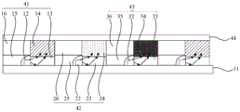
本发明的实施例还提出了一种显示装置。如图4所示,该显示装置包括基板11、至少一个像素(未示出)以及封装层44。Embodiments of the present invention also provide a display device. As shown in FIG. 4 , the display device includes a
如图4所示,上述的至少一个像素位于基板11上。每个像素包括第一子像素41、第二子像素42与第三子像素43。第一子像素41用于发射红光,第二子像素42用于发绿光,第三子像素43用于发射蓝光。As shown in FIG. 4 , the above-mentioned at least one pixel is located on the
如图4所示,第一子像素41包括第一发光二极管芯片12、第一光线调整结构13与第一光转换结构14。本实施例中的第一子像素41与上述的面光源相似,第一发光二极管芯片12位于基板11上,用于发射第一颜色的光,第一光线调整结构13位于基板11上,且与第一发光二极管芯片12相邻,用于将从第一发光二极管芯片12接收的第一颜色的光均匀地从远离基板11的表面射出,第一光转换结构14位于第一光线调整结构13远离基板11的一侧,用于将从第一光线调整结构13接收的第一颜色的光转换为第二颜色的光,并从远离基板11的表面射出,第一颜色的光的颜色与第二颜色的光的颜色不同。As shown in FIG. 4 , the
在本实施例中,第一发光二极管芯片12为蓝光芯片,第一颜色的光为蓝光,第二颜色的光为红光。亦即,第一发光二极管芯片12用于发射蓝光,第一光转换结构14用于将蓝光转换为红光。In this embodiment, the first light emitting
如图4所示,第一子像素41还包括第一挡墙15与第二挡墙16;第一挡墙15位于第一发光二极管芯片12远离第一光线调整结构13的一侧,用于将来自第一发光二极管芯片12的第一颜色的光反射至第一光线调整结构13;第二挡墙16位于第一挡墙15远离基板11的一侧,第二挡墙16用于遮光。As shown in FIG. 4 , the
如图4所示,第二子像素42与第一子像素41相似,第二子像素42包括第二发光二极管芯片22、第二光线调整结构23与第二光转换结构24,第二发光二极管芯片22位于基板11上,用于发射第一颜色的光,即,用于发蓝光。第二光线调整结构23位于基板11上,且与第二发光二极管芯片22相邻,用于将从第二发光二极管芯片22接收的第一颜色的光均匀地从远离基板11的表面射出,第二光转换结构24位于第二光线调整结构23远离基板11的一侧,用于将从第二光线调整结构23接收的第一颜色的光转换为第三颜色的光,并从远离基板11的表面射出,第一颜色的光的颜色与第三颜色的光的颜色不同。第二发光二极管芯片22为蓝光芯片,第三颜色的光为绿光。即,第二光转换结构24用于将蓝光转换为绿光。As shown in FIG. 4 , the
如图4所示,第二子像素42还包括第三挡墙25与第四挡墙26。第三挡墙25与第一挡墙15结构相同,第四挡墙26与第二挡墙16结构相同。第三挡墙25位于第二发光二极管芯片22远离第二光线调整结构23的一侧,用于将来自第二发光二极管芯片22的光反射至第二光线调整结构23;第四挡墙26位于第三挡墙23远离基板11的一侧,第四挡墙26用于遮光。As shown in FIG. 4 , the
如图4所示,第三子像素43包括第三发光二极管芯片32、第三光线调整结构33与第二散射膜34,第三发光二极管芯片32位于基板11上,用于发射第一颜色的光,即,第三发光二极管芯片32用于发射蓝光。第三光线调整结构33位于基板11上,且与第三发光二极管芯片32相邻,用于将从第三发光二极管芯片32接收的第一颜色的光均匀地从远离基板11的表面射出,第二散射膜34位于第三光线调整结构33远离基板11的一侧,用于将从第三光线调整结构33接收的第一颜色的光均匀地从远离基板11的表面射出。第三发光二极管芯片32为蓝光芯片。As shown in FIG. 4 , the
在本实施例中,第二散射膜34为包括有散射粒子的透明胶层。其中,散射粒子的材料可以为TiO2或SiO2。第二散射膜34使第三子像素43发射的光的分布与第一子像素41发射的光的分布、第二子像素42发射的光的分布相同,均为高斯分布,有利于提升显示效果。In this embodiment, the
如图4所示,第三子像素43还包括第五挡墙35与第六挡墙36。第五挡墙35与第一挡墙15结构相同,第六挡墙36与第二挡墙16结构相同。第五挡墙35位于第三发光二极管芯片32远离第三光线调整结构33的一侧,用于将来自第三发光二极管芯片32的第一颜色的光反射至第三光线调整结构33;第六挡墙36位于第五挡墙35远离基板11的一侧,第六挡墙36用于遮光。As shown in FIG. 4 , the
在本实施例中,第二挡墙16、第四挡墙26与第六挡墙36可以防止第一子像素41、第二子像素42与第三子像素43发射的光串色,降低显示装置的色域。In this embodiment, the
在本实施例中,第一光线调整结构13、第二光线调整结构23与第三光线调整结构33采用显示装置的制程中的工艺制备,而不是单独制备后放置在基板11上。In this embodiment, the first
在本实施例中,蓝光芯片为倒装芯片。这样,蓝光芯片可向四周发射蓝光。In this embodiment, the blue light chip is a flip chip. In this way, the blue light chip can emit blue light all around.
由于量子点的材料本身的特性,其对蓝光照射很敏感,长时间高能蓝光照射会对量子点的材料造成伤害,显示装置做成如图4所示的结构,一方面是可以增加光程,减少蓝光芯片对量子点的性能损坏,另一方面在图5中有示意,可以充分利用倒装芯片的侧面的光线,提升效率,减少整体功耗。Due to the characteristics of the material of quantum dots, they are very sensitive to blue light irradiation. Long-term high-energy blue light irradiation will cause damage to the material of quantum dots. The display device is made into the structure shown in Figure 4. To reduce the performance damage of the blue light chip to the quantum dots, on the other hand, as shown in Figure 5, the light on the side of the flip chip can be fully utilized to improve the efficiency and reduce the overall power consumption.
在本实施例中,封装层44位于像素远离基板11的一侧,用于隔离水氧。封装层44的材料可以是氮化硅。由于氮化硅的致密性比较好,因此,封装层44可以隔离水氧,保护像素,延长显示装置的寿命。In this embodiment, the
在本实施例中,封装层44通过磁控溅射实现或低温化学气相沉积(CVD)来实现。In this embodiment, the
在本实施例中,由于第一子像素41使用的是蓝光芯片而不是红光芯片,而蓝光芯片的良率比红光芯片的良率高,因此,可以提高显示装置的良率、降低成本。In this embodiment, since the
在本实施例中,每个像素中第一子像素41、第二子像素42、第三子像素43均使用蓝光芯片,这样,可以提高产能及效率。In this embodiment, the
在本实施例中,第三挡墙25还可以将第一发光二极管芯片12发射的光反射至第一光线调整结构13,可以提升蓝光的利用效率。同理,第五挡墙35还可以将第二发光二极管芯片22发射的光反射至第二光线调整结构23,可以提升蓝光的利用效率。In this embodiment, the
本发明的实施例还提出了一种显示装置。本实施例与上述实施例不同的是,在本实施例中,第二发光二极管芯片22用于发射绿光。Embodiments of the present invention also provide a display device. The difference between this embodiment and the above-mentioned embodiment is that in this embodiment, the second light emitting
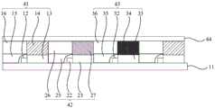
如图6所示,第二子像素27包括第二发光二极管芯片22、第二光线调整结构23与第一散射膜27。第二发光二极管芯片22位于基板11上,用于发射第三颜色的光,第二光线调整结构23位于基板11上,且与第二发光二极管芯片22相邻,用于将从第二发光二极管芯片22接收的第三颜色的光均匀地从远离基板11的表面射出,第一散射膜27位于第二光线调整结构22远离基板11的一侧,用于将从第二光线调整结构23接收的第三颜色的光均匀地从远离基板11的表面射出。第二发光二极管芯片22为绿光芯片,第三颜色的光为绿光。即,第二子像素27用于发射绿光。第二发光二极管芯片22用于发射绿光。As shown in FIG. 6 , the
在本实施例中,第一散射膜27与上述的第二散射膜34相似,为包括有散射粒子的透明胶层。其中,散射粒子的材料可以为TiO2或SiO2。In this embodiment, the
本发明的实施例还提出了一种面光源的制备方法,用于制备上述的面光源。如图7所示,包括以下步骤701~703:The embodiments of the present invention also provide a method for preparing a surface light source, which is used for preparing the above-mentioned surface light source. As shown in FIG. 7 , the following
在步骤701中,在基板上形成第一发光二极管芯片,第一发光二极管芯片用于发射第一颜色的光。In
在步骤702中,形成第一光线调整结构,第一光线调整结构位于基板上,且与第一发光二极管芯片相邻,用于将从第一发光二极管芯片接收的第一颜色的光均匀地从远离基板的表面射出。In
在步骤703中,形成第一光转换结构,第一光转换结构位于第一光线调整结构远离基板的一侧,用于将从第一光线调整结构接收的第一颜色的光转换为第二颜色的光,并从远离基板的表面射出,第一颜色的光的颜色与第二颜色的光的颜色不同。In
在本实施例中,由于第一发光二极管芯片位于基板上,用于发射第一颜色的光,第一光线调整结构位于基板上,且与第一发光二极管芯片相邻,用于将从第一发光二极管芯片接收的第一颜色的光均匀地从远离基板的表面射出,以形成面光源,第一光转换结构位于第一光线调整结构远离基板的一侧,用于将从第一光线调整结构接收的第一颜色的光转换为第二颜色的光,并从远离基板的表面射出,这样,当发射第二颜色的光的发光二极管芯片良率低、成本高时,可以利用发射第一颜色的光的第一发光二极管芯片以及用于将第一颜色的光转换为第二颜色的光的第一光转换结构来获取第二颜色的光,而无需使用发射第二颜色的光的发光二极管芯片,因此,可以提高面光源的良率、降低面光源的成本,进而可以提高显示装置的良率、降低成本。In this embodiment, since the first light emitting diode chip is located on the substrate and is used for emitting light of the first color, the first light adjusting structure is located on the substrate and adjacent to the first light emitting diode chip, and is used to transmit light from the first light emitting diode chip. The light of the first color received by the light-emitting diode chip is uniformly emitted from the surface away from the substrate to form a surface light source, and the first light conversion structure is located on the side of the first light adjustment structure away from the substrate, and is used to convert the first light adjustment structure from the first light adjustment structure. The received light of the first color is converted into light of the second color, and is emitted from the surface away from the substrate, so that when the light-emitting diode chip that emits the light of the second color has a low yield and high cost, it can be used to emit light of the first color. a first light emitting diode chip of light and a first light conversion structure for converting light of a first color into light of a second color to obtain light of the second color without using light emitting diodes emitting light of the second color Therefore, the yield of the surface light source can be improved, the cost of the surface light source can be reduced, and the yield of the display device can be improved and the cost can be reduced.
需要说明的是,本实施例中的显示装置可以为:电子纸、手机、平板电脑、电视机、笔记本电脑、数码相框、导航仪等任何具有显示功能的产品或部件。It should be noted that the display device in this embodiment may be any product or component with display function, such as electronic paper, mobile phone, tablet computer, television, notebook computer, digital photo frame, and navigator.
其中,上述流程所采用的形成工艺例如可包括:沉积、溅射等成膜工艺和刻蚀等构图工艺。The formation process used in the above process may include, for example, film formation processes such as deposition and sputtering, and patterning processes such as etching.
需要指出的是,在附图中,为了图示的清晰可能夸大了层和区域的尺寸。而且可以理解,当元件或层被称为在另一元件或层“上”时,它可以直接在其他元件上,或者可以存在中间的层。另外,可以理解,当元件或层被称为在另一元件或层“下”时,它可以直接在其他元件下,或者可以存在一个以上的中间的层或元件。另外,还可以理解,当层或元件被称为在两层或两个元件“之间”时,它可以为两层或两个元件之间唯一的层,或还可以存在一个以上的中间层或元件。通篇相似的参考标记指示相似的元件。It should be noted that, in the drawings, the sizes of layers and regions may be exaggerated for clarity of illustration. It will also be understood that when an element or layer is referred to as being "on" another element or layer, it can be directly on the other element or intervening layers may be present. In addition, it will be understood that when an element or layer is referred to as being "under" another element or layer, it can be directly under the other element, or more than one intervening layer or element may be present. In addition, it will also be understood that when a layer or element is referred to as being 'between' two layers or elements, it can be the only layer between the two layers or elements, or more than one intervening layer may also be present or components. Like reference numerals indicate like elements throughout.
在本发明中,术语“第一”、“第二”仅用于描述目的,而不能理解为指示或暗示相对重要性。术语“多个”指两个或两个以上,除非另有明确的限定。In the present invention, the terms "first" and "second" are used for descriptive purposes only, and cannot be understood as indicating or implying relative importance. The term "plurality" refers to two or more, unless expressly limited otherwise.
本领域技术人员在考虑说明书及实践这里公开的公开后,将容易想到本发明的其它实施方案。本发明旨在涵盖本发明的任何变型、用途或者适应性变化,这些变型、用途或者适应性变化遵循本发明的一般性原理并包括本发明未公开的本技术领域中的公知常识或惯用技术手段。说明书和实施例仅被视为示例性的,本发明的真正范围和精神由下面的权利要求指出。Other embodiments of the invention will readily suggest themselves to those skilled in the art upon consideration of the specification and practice of the disclosure disclosed herein. The present invention is intended to cover any variations, uses or adaptations of the present invention which follow the general principles of the invention and which include common knowledge or conventional techniques in the technical field not disclosed by the present invention . The specification and examples are to be regarded as exemplary only, with the true scope and spirit of the invention being indicated by the following claims.
应当理解的是,本发明并不局限于上面已经描述并在附图中示出的精确结构,并且可以在不脱离其范围进行各种修改和改变。本发明的范围仅由所附的权利要求来限制。It should be understood that the present invention is not limited to the precise structures described above and illustrated in the accompanying drawings, and that various modifications and changes may be made without departing from its scope. The scope of the present invention is limited only by the appended claims.
Claims (15)
Translated fromChinesePriority Applications (1)
| Application Number | Priority Date | Filing Date | Title |
|---|---|---|---|
| CN202011005443.1ACN112037674B (en) | 2020-09-22 | 2020-09-22 | Surface light source, preparation method thereof, and display device |
Applications Claiming Priority (1)
| Application Number | Priority Date | Filing Date | Title |
|---|---|---|---|
| CN202011005443.1ACN112037674B (en) | 2020-09-22 | 2020-09-22 | Surface light source, preparation method thereof, and display device |
Publications (2)
| Publication Number | Publication Date |
|---|---|
| CN112037674Atrue CN112037674A (en) | 2020-12-04 |
| CN112037674B CN112037674B (en) | 2022-09-06 |
Family
ID=73574192
Family Applications (1)
| Application Number | Title | Priority Date | Filing Date |
|---|---|---|---|
| CN202011005443.1AActiveCN112037674B (en) | 2020-09-22 | 2020-09-22 | Surface light source, preparation method thereof, and display device |
Country Status (1)
| Country | Link |
|---|---|
| CN (1) | CN112037674B (en) |
Cited By (2)
| Publication number | Priority date | Publication date | Assignee | Title |
|---|---|---|---|---|
| CN112614957A (en)* | 2020-12-07 | 2021-04-06 | 厦门天马微电子有限公司 | Display panel and display device |
| CN115332235A (en)* | 2022-07-13 | 2022-11-11 | 盐城东山精密制造有限公司 | A mini-cob light panel and its production process |
Citations (12)
| Publication number | Priority date | Publication date | Assignee | Title |
|---|---|---|---|---|
| JP2001210871A (en)* | 2000-01-25 | 2001-08-03 | Sharp Corp | Side emission type light emitting diode, method for manufacturing the same, and portable terminal device provided with this side emission type light emitting diode |
| CN1598670A (en)* | 2003-09-19 | 2005-03-23 | 鸿富锦精密工业(深圳)有限公司 | Area source device |
| CN201628178U (en)* | 2009-12-31 | 2010-11-10 | 深圳市山本光电有限公司 | Light guide plate |
| CN102130273A (en)* | 2010-12-10 | 2011-07-20 | 深圳市华星光电技术有限公司 | Light-emitting diode packaging structure |
| CN102866535A (en)* | 2011-07-05 | 2013-01-09 | 乐金显示有限公司 | Liquid crystal display panel including photo conversion layer and liquid crystal display device |
| JP2013243306A (en)* | 2012-05-22 | 2013-12-05 | Mitsubishi Electric Corp | Led light source and manufacturing method of the same |
| CN104832887A (en)* | 2014-02-11 | 2015-08-12 | 宏达国际电子股份有限公司 | Light source module and electronic device |
| CN109426046A (en)* | 2017-08-25 | 2019-03-05 | 京东方科技集团股份有限公司 | Display device and display device |
| CN110441956A (en)* | 2019-08-20 | 2019-11-12 | 苏州星烁纳米科技有限公司 | Quantum stippling film and display device |
| CN110875360A (en)* | 2018-08-31 | 2020-03-10 | 昆山工研院新型平板显示技术中心有限公司 | Display panel |
| CN210639385U (en)* | 2019-08-20 | 2020-05-29 | 苏州星烁纳米科技有限公司 | Quantum dot color film and display device |
| CN111509025A (en)* | 2020-05-26 | 2020-08-07 | 京东方科技集团股份有限公司 | Quantum dot-based display panel, preparation method thereof, and display device |
- 2020
- 2020-09-22CNCN202011005443.1Apatent/CN112037674B/enactiveActive
Patent Citations (12)
| Publication number | Priority date | Publication date | Assignee | Title |
|---|---|---|---|---|
| JP2001210871A (en)* | 2000-01-25 | 2001-08-03 | Sharp Corp | Side emission type light emitting diode, method for manufacturing the same, and portable terminal device provided with this side emission type light emitting diode |
| CN1598670A (en)* | 2003-09-19 | 2005-03-23 | 鸿富锦精密工业(深圳)有限公司 | Area source device |
| CN201628178U (en)* | 2009-12-31 | 2010-11-10 | 深圳市山本光电有限公司 | Light guide plate |
| CN102130273A (en)* | 2010-12-10 | 2011-07-20 | 深圳市华星光电技术有限公司 | Light-emitting diode packaging structure |
| CN102866535A (en)* | 2011-07-05 | 2013-01-09 | 乐金显示有限公司 | Liquid crystal display panel including photo conversion layer and liquid crystal display device |
| JP2013243306A (en)* | 2012-05-22 | 2013-12-05 | Mitsubishi Electric Corp | Led light source and manufacturing method of the same |
| CN104832887A (en)* | 2014-02-11 | 2015-08-12 | 宏达国际电子股份有限公司 | Light source module and electronic device |
| CN109426046A (en)* | 2017-08-25 | 2019-03-05 | 京东方科技集团股份有限公司 | Display device and display device |
| CN110875360A (en)* | 2018-08-31 | 2020-03-10 | 昆山工研院新型平板显示技术中心有限公司 | Display panel |
| CN110441956A (en)* | 2019-08-20 | 2019-11-12 | 苏州星烁纳米科技有限公司 | Quantum stippling film and display device |
| CN210639385U (en)* | 2019-08-20 | 2020-05-29 | 苏州星烁纳米科技有限公司 | Quantum dot color film and display device |
| CN111509025A (en)* | 2020-05-26 | 2020-08-07 | 京东方科技集团股份有限公司 | Quantum dot-based display panel, preparation method thereof, and display device |
Cited By (3)
| Publication number | Priority date | Publication date | Assignee | Title |
|---|---|---|---|---|
| CN112614957A (en)* | 2020-12-07 | 2021-04-06 | 厦门天马微电子有限公司 | Display panel and display device |
| CN112614957B (en)* | 2020-12-07 | 2023-07-18 | 厦门天马微电子有限公司 | A display panel and a display device |
| CN115332235A (en)* | 2022-07-13 | 2022-11-11 | 盐城东山精密制造有限公司 | A mini-cob light panel and its production process |
Also Published As
| Publication number | Publication date |
|---|---|
| CN112037674B (en) | 2022-09-06 |
Similar Documents
| Publication | Publication Date | Title |
|---|---|---|
| JP7484727B2 (en) | Light emitting device and image display device | |
| JP7414886B2 (en) | Light emitting device and its manufacturing method | |
| CN110993756B (en) | LED chip and manufacturing method thereof | |
| TWI805028B (en) | Display substrate and display device | |
| CN214848634U (en) | Light-emitting module and display device | |
| TW201729434A (en) | Light-emitting element and method of manufacturing same | |
| CN117995869A (en) | Chip structure, manufacturing method and display device | |
| CN112582441B (en) | Display panel, display device and preparation method of display panel | |
| CN215869440U (en) | Light emitting element, unit pixel and display device | |
| JP7666496B2 (en) | Light emitting device and method for manufacturing the same | |
| CN112037674B (en) | Surface light source, preparation method thereof, and display device | |
| CN115347015B (en) | Light-emitting element and display device | |
| US10663794B2 (en) | Display devices | |
| CN112310142A (en) | Display device, display panel and manufacturing method thereof | |
| CN114326206B (en) | Display device | |
| US11742377B2 (en) | Light emitting diode chip, display device and method for manufacturing the same | |
| CN114068607B (en) | Display substrate, manufacturing method thereof, and display device | |
| CN215184028U (en) | Light-emitting devices and display devices | |
| CN115548233A (en) | Display panel, display device and manufacturing method of display panel | |
| US20240145439A1 (en) | Light-emitting diode devices with support elements for improved near-field and far-field emissions | |
| US20220199857A1 (en) | Unit pixel and displaying apparatus including the unit pixel | |
| US20240328595A1 (en) | Light-emitting device and image display apparatus | |
| TW202515422A (en) | Luminescent chip, display substrate and display device | |
| CN118538749A (en) | Display panel, manufacturing method thereof and electronic equipment | |
| CN117525241A (en) | Light-emitting module and display device |
Legal Events
| Date | Code | Title | Description |
|---|---|---|---|
| PB01 | Publication | ||
| PB01 | Publication | ||
| SE01 | Entry into force of request for substantive examination | ||
| SE01 | Entry into force of request for substantive examination | ||
| GR01 | Patent grant | ||
| GR01 | Patent grant |