CN112019071A - power converter - Google Patents
power converterDownload PDFInfo
- Publication number
- CN112019071A CN112019071ACN202010668647.7ACN202010668647ACN112019071ACN 112019071 ACN112019071 ACN 112019071ACN 202010668647 ACN202010668647 ACN 202010668647ACN 112019071 ACN112019071 ACN 112019071A
- Authority
- CN
- China
- Prior art keywords
- voltage
- input
- converter
- coupled
- power converter
- Prior art date
- Legal status (The legal status is an assumption and is not a legal conclusion. Google has not performed a legal analysis and makes no representation as to the accuracy of the status listed.)
- Pending
Links
- 238000004146energy storageMethods0.000claimsabstractdescription45
- 230000005856abnormalityEffects0.000claimsabstractdescription9
- 239000003990capacitorSubstances0.000description55
- 230000002159abnormal effectEffects0.000description24
- 101100277795Arabidopsis thaliana PFC1 geneProteins0.000description14
- 238000010586diagramMethods0.000description7
- 238000006243chemical reactionMethods0.000description6
- 230000017525heat dissipationEffects0.000description3
- 238000013461designMethods0.000description2
- 238000000034methodMethods0.000description2
- 230000010363phase shiftEffects0.000description2
- 238000011084recoveryMethods0.000description2
- 230000004913activationEffects0.000description1
- 230000033228biological regulationEffects0.000description1
- 239000004568cementSubstances0.000description1
- 230000003247decreasing effectEffects0.000description1
- 238000001514detection methodMethods0.000description1
- 238000005516engineering processMethods0.000description1
- 238000002474experimental methodMethods0.000description1
- 230000006872improvementEffects0.000description1
- 238000012986modificationMethods0.000description1
- 230000004048modificationEffects0.000description1
- 230000008569processEffects0.000description1
- 238000012545processingMethods0.000description1
- 238000005070samplingMethods0.000description1
- 239000004065semiconductorSubstances0.000description1
- 238000006467substitution reactionMethods0.000description1
- 230000007704transitionEffects0.000description1
- 238000004804windingMethods0.000description1
Images


Landscapes
- Dc-Dc Converters (AREA)
- Rectifiers (AREA)
Abstract
Translated fromChinese
Description
Translated fromChinese本申请为于2015年7月29日提交、申请号为201510456621.5、发明名称为“电源转换器”的中国专利申请的分案申请。This application is a divisional application of a Chinese patent application filed on July 29, 2015 with the application number of 201510456621.5 and the invention name of "power converter".
技术领域technical field
本发明涉及电气技术领域,更具体而言涉及一种电源转换器,尤其涉及一种具有期望的保持时间的同时具有提高的功率密度的电源转换器。The present invention relates to the field of electrical technology, and more particularly, to a power converter, and in particular, to a power converter with a desired hold time and improved power density.
背景技术Background technique
目前,诸如计算机等的一部分电子设备对电源的稳定性的要求越来越高,由其是在输入电压异常时(例如掉电时),需要在输入电压发生异常后能够在一定时间内将输出电压维持在特定范围内,这段时间被称为保持时间,用于在线路故障后顺序终止数据处理装置的操作或者切换到不间断电源(UPS)操作。At present, some electronic devices such as computers have higher and higher requirements on the stability of the power supply, because when the input voltage is abnormal (such as power failure), it is necessary to be able to output the output within a certain period of time after the abnormal input voltage occurs. The voltage is maintained within a specified range, a period of time known as the hold-up time, and is used to sequentially terminate operation of the data processing device or switch to uninterruptible power supply (UPS) operation following a line failure.
现以交流-直流电源转换器为例进行说明。通常,交流-直流电源转换器包括:全波整流器、电压转换器以及直流-直流(DC-DC)转换电路。电压转换器耦接在全波整流器与DC-DC转换电路之间,用于使从全波整流器输出的电源信号经过升压或降压后,向DC-DC转换电路输出直流电源信号。在电压转换器之后配置有输出储能元件,例如电容C,用于平衡输入、输出的瞬时功率,滤除二次谐波纹波,以及使电源转换器具有足够的保持时间。Now take an AC-DC power converter as an example to illustrate. Typically, an AC-DC power converter includes a full-wave rectifier, a voltage converter, and a direct current-to-direct current (DC-DC) conversion circuit. The voltage converter is coupled between the full-wave rectifier and the DC-DC conversion circuit, and is used to output the DC power signal to the DC-DC conversion circuit after the power signal output from the full-wave rectifier is boosted or stepped down. After the voltage converter, an output energy storage element, such as a capacitor C, is configured to balance the instantaneous power of the input and output, filter out the second harmonic ripple, and make the power converter have sufficient hold-up time.
在常见的设计中,在输入电压发生异常期间,借助存储在储能电容C中的能量维持可以在一段时间内维持输出电压,直到储能电容C的电压低于后端的DC-DC转换电路的最低工作电压。由于,这个最低工作电源远高于储能电容C完全放电的电压(零电压),因而,存储在储能电容C的能量仅有一部分可以用于维持输出电压。例如,针对高效率AC-DC电源转换器,当储能电容C的电压为390V,而后端的DC-DC转换电路的最低工作电压是280V时,在输入电压发生异常期间,仅有大约48%的存储在储能电容C中能量可以被利用。In a common design, when the input voltage is abnormal, the output voltage can be maintained for a period of time with the help of the energy stored in the energy storage capacitor C, until the voltage of the energy storage capacitor C is lower than the back-end DC-DC conversion circuit. Minimum operating voltage. Since this minimum working power is much higher than the voltage at which the storage capacitor C is fully discharged (zero voltage), only a part of the energy stored in the storage capacitor C can be used to maintain the output voltage. For example, for a high-efficiency AC-DC power converter, when the voltage of the energy storage capacitor C is 390V, and the minimum operating voltage of the back-end DC-DC conversion circuit is 280V, during the abnormal input voltage period, only about 48% of the The energy stored in the storage capacitor C can be utilized.
为了更大限度地利用存储的能量,需要应用更大的储能电容。然而,作为储能电容的电解电容通常体积较大,并且相应的散热器也占据了较大的位置,这成为影响电源功率密度的进一步提高的主要因素。In order to maximize the utilization of the stored energy, a larger storage capacitor needs to be applied. However, the electrolytic capacitors used as energy storage capacitors are usually bulky, and the corresponding heat sinks also occupy a large position, which becomes the main factor affecting the further improvement of the power density of the power supply.
发明内容SUMMARY OF THE INVENTION
本发明的目的之一在于提供一种电源转换器,以期望解决上述现有技术中的问题。One of the objectives of the present invention is to provide a power converter, which is expected to solve the above-mentioned problems in the prior art.
根据本发明的一个方面,提供了一种电源转换器,包括:第一输入整流器和第二输入整流器,用于从输入电压产生经整流的输入电压;交错并联地耦接在电源转换器的输入端与直流输出端之间的第一电压转换器和第二电压转换器,用于将经整流的输入电压转换为直流输出电压,其中,第一电压转换器的输入端与第一输入整流器耦接,第二电压转换器的输入端与第二输入整流器耦接;第一储能元件,耦接在第一电压转换器的输出端与电源转换器的接地端之间;第二储能元件,耦接在第二电压转换器的输出端与电源转换器的接地端之间;输出控制单元,输出控制单元耦接在第一电压转换器的输出端和第二电压转换器的输出端之间,用于在输入电压发生异常期间,断开第一电压转换器和第二电压转换器的输出端的之间的连接;以及旁路单元,耦接在第二储能元件与第一电压转换器的输入端之间,用于在输入电压发生异常期间,使得存储在第二储能元件中的能量经由旁路单元向第一储能元件传送。According to one aspect of the present invention, there is provided a power converter comprising: a first input rectifier and a second input rectifier for generating a rectified input voltage from an input voltage; coupled in interleaved parallel at the input of the power converter A first voltage converter and a second voltage converter between the terminal and the DC output terminal for converting the rectified input voltage to a DC output voltage, wherein the input terminal of the first voltage converter is coupled to the first input rectifier The input terminal of the second voltage converter is coupled to the second input rectifier; the first energy storage element is coupled between the output terminal of the first voltage converter and the ground terminal of the power converter; the second energy storage element , coupled between the output end of the second voltage converter and the ground end of the power converter; the output control unit, the output control unit is coupled between the output end of the first voltage converter and the output end of the second voltage converter time, for disconnecting the connection between the output terminals of the first voltage converter and the second voltage converter when the input voltage is abnormal; and a bypass unit, coupled between the second energy storage element and the first voltage converter Between the input ends of the device, the energy stored in the second energy storage element is transmitted to the first energy storage element via the bypass unit during the abnormal period of the input voltage.
根据本发明实施例的电源转换器,通过将存储在第二储能元件上的能量传送到第一储能元件上,使得获得同样的保持时间所需的储能元件的容量更小,从而提高了电源转换器的功率密度并同时改善了电路的散热。According to the power converter of the embodiment of the present invention, by transferring the energy stored in the second energy storage element to the first energy storage element, the capacity of the energy storage element required to obtain the same holding time is smaller, thereby improving the The power density of the power converter is improved while the heat dissipation of the circuit is improved.
附图说明Description of drawings
本公开可以通过参考下文中结合附图所给出的描述而得到更好的理解,其中在所有附图中使用了相同或相似的附图标记来表示相同或者相似的部件。所述附图连同下面的详细说明一起包含在本说明书中并且形成本说明书的一部分,而且用来进一步举例说明本公开的优选实施例和解释本公开的原理和优点。在附图中:The present disclosure may be better understood by reference to the description given below in connection with the accompanying drawings, wherein the same or like reference numerals are used throughout the drawings to refer to the same or like parts. The accompanying drawings, together with the following detailed description, are incorporated in and form a part of this specification, and are used to further illustrate preferred embodiments of the disclosure and to explain the principles and advantages of the disclosure. In the attached image:
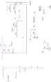
图1是根据本发明一个实施例的电源转换器的示意性结构框图;1 is a schematic structural block diagram of a power converter according to an embodiment of the present invention;
图2是根据本发明一个实施例的电源转换器的具体电路图;2 is a specific circuit diagram of a power converter according to an embodiment of the present invention;
图3是采用绝缘栅双极型晶体管(IGBT)作为开关元件Q1的驱动电路图;FIG. 3 is a driving circuit diagram using an insulated gate bipolar transistor (IGBT) as the switching element Q1;
图4A示意性地示出了不具有旁路单元的电源转换器在输入电压异常期间的输出电压曲线;FIG. 4A schematically shows an output voltage curve of a power converter without a bypass unit during an abnormal input voltage;
图4B示意性地示出了具有旁路单元的电源转换器在输入电压异常期间的输出电压曲线。FIG. 4B schematically shows an output voltage curve of a power converter with a bypass unit during an abnormal input voltage.
图5示意性的示出了输入电压发生异常后(未恢复)的时序;FIG. 5 schematically shows the time sequence after the input voltage is abnormal (not restored);
图6示意性的示出了输入电压在发生异常后又恢复的时序。FIG. 6 schematically shows the timing of the restoration of the input voltage after an abnormality occurs.
具体实施例specific embodiment
在下文中,将参考附图详细地描述本发明的实施例。Hereinafter, embodiments of the present invention will be described in detail with reference to the accompanying drawings.
本领域技术人员可以理解,本发明中的“第一”、“第二”等术语仅用于区别不同单元、模块或步骤等,既不代表任何特定技术含义,也不表示它们之间的必然逻辑顺序,也不体现其所限定的不同单元、模块或步骤的重要性程度。Those skilled in the art can understand that terms such as "first" and "second" in the present invention are only used to distinguish different units, modules or steps, etc., and neither represent any specific technical meaning nor an inevitable relationship between them. The logical sequence does not reflect the importance of the different units, modules or steps defined by them.
应理解当元件被称为与另外的元件“连接”或“耦接”时,其可以直接地与其他元件连接或耦接或者可以存在介于中间的元件。相反,当元件被称为与另外的元件“直接地连接”或“直接地耦接”时,不存在介于中间的元件。用于描述元件之间的关系的其他术语应以类似的方式被解释(例如,“在…之间”相对“直接地在…之间”,“相邻”相对于“直接地相邻”等)。It will be understood that when an element is referred to as being "connected" or "coupled" to another element, it can be directly connected or coupled to the other element or intervening elements may be present. In contrast, when an element is referred to as being "directly connected" or "directly coupled" to another element, there are no intervening elements present. Other terms used to describe the relationship between elements should be interpreted in a like fashion (eg, "between" versus "directly between," "adjacent" versus "directly adjacent," etc. ).
图1是根据本发明一个实施例的电源转换器的示意性结构框图。本实施例公开的电源转换器,包括:第一输入整流器110、第二输入整流器120、第一电压转换器112、第二电压转换器122、第一储能元件C1、第二储能元件C2、输出控制单元130和旁路单元140。FIG. 1 is a schematic structural block diagram of a power converter according to an embodiment of the present invention. The power converter disclosed in this embodiment includes: a
第一输入整流器110和第二输入整流器120与输入电压vi耦接,用于从输入电压产生经整流的输入电压。The
第一电压转换器112和第二电压转换器122视具体情况可以是升压转换器或降压转换器,用于将经整流的输入电压经升压或降压后转换为直流输出电压vout,以便供后端使用。The
第一电压转换器112的输入端与第一输入整流器110的输出端耦接,第一电源转换器112的输出端与电源转换器的直流输出端vout耦接。第二电压转换器122的输入端与第一输入整流器120的输出端vout耦接,第二电源转换器122的输出端与电源转换器的直流输出端vout耦接。第一电压转换器112与第二电压转换器122相互并联连接,并以180°的相移交替工作,从而构成交错并联结构。The input terminal of the
第一储能元件C1耦接在第一电压转换器112的输出端与电源转换器的接地端之间。第二储能元件C2耦接在第二电压转换器122的输出端与电源转换器的接地端之间。第一、第二储能元件C1、C2用于向后端提供能量。The first energy storage element C1 is coupled between the output terminal of the
输出控制单元130耦接在第一电压转换器112的输出端和第二电压转换器122的输出端之间,在电源转换器正常工作期间,输出控制单元130使得第一电压转换器112的输出端和第二电压转换器122的输出端处于导通状态,第一电压转换器112和第二电压转换器122并联连接,二者交替工作。而在输入电压发生异常期间(在本例中例如为输入电压突然断开或大幅下降等),输出控制单元130用于断开第一电压转换器112的输出端和第二电压转换器122的输出端的之间的连接。The
旁路单元140耦接在第二储能元件C2与第一电压转换器112的输入端之间。在电源转换器正常工作期间,旁路单元140不工作,第一、第二储能元件C1、C2共同向后端提供能量。而在输入电压发生异常期间,旁路单元140处于工作状态,使得存储在第二储能元件C2中的能量经由旁路单元140向第一储能元件C1传送,以便维持第一储能元件C1电压稳定,并向后端提供输出电压。The
本实施例中公开的电源转换器中,在输入电压发生异常期间,通过旁路单元将本来并联连接的两个电压转换器改成串联连接的形式,将存储在第二储能元件C2上的能量传送到第一储能元件C1上,使得获得同样的保持时间所需的储能元件的容量更小,从而改善电路的散热并提高电路的功率密度。In the power converter disclosed in this embodiment, during the period when the input voltage is abnormal, the two voltage converters originally connected in parallel are changed to be connected in series through the bypass unit, and the voltage stored in the second energy storage element C2 is converted into The energy is transferred to the first energy storage element C1, so that the capacity of the energy storage element required to obtain the same holding time is smaller, thereby improving the heat dissipation of the circuit and increasing the power density of the circuit.
以上描述虽然是借助交流-直流电源转换器展开的,但本领域技术人员应知晓本发明的实施例的应用并不限于交流-直流电源转换器,其同样可以作为直流-直流电源转换器的一部分。Although the above description is based on the AC-DC power converter, those skilled in the art should know that the application of the embodiments of the present invention is not limited to the AC-DC power converter, and it can also be used as a part of the DC-DC power converter. .
由上述描述可了解本发明一个实施例的电路构造,以下结合图2说明其实际运用的具体电路图。其中,图2是根据本发明一个实施例的电源转换器的具体电路图。The circuit structure of an embodiment of the present invention can be understood from the above description, and a specific circuit diagram of its practical application will be described below with reference to FIG. 2 . 2 is a specific circuit diagram of a power converter according to an embodiment of the present invention.
第一输入整流器110和第二输入整流器120可以是全桥整流器D7、D8,用于从输入的交流电压(AC-INPUT)产生经整流的输入电压。The
第一电压转换器112和第二电压转换器122可以是功率因数调整(PFC)电路。如图2所示,第一PFC单元PFC1耦接在第一输入整流器D7与电源转换器的直流输出端(V-BULK)之间,并且至少包括电感L1、二极管D4、开关元件Q2。第二PFC单元PFC2耦接在第二输入整流器D8与电源转换器的直流输出端(V-BULK)之间,并且至少包括电感L2、二极管D6、开关元件Q3。The
可选地,可以在第二PFC单元PFC2的电感L2和二极管D6两端并联连接二极管D3。在这种情况下,在交流电压输入(恢复)瞬间,输入电压可以经由二极管D3对给第二储能元件C2进行充电,以防止电感L2、二极管D6以及开关元件Q3受到浪涌电流的冲击。Optionally, a diode D3 may be connected in parallel across the inductor L2 and the diode D6 of the second PFC unit PFC2. In this case, at the moment of AC voltage input (recovery), the input voltage can charge the second energy storage element C2 via the diode D3 to prevent the inductor L2, the diode D6 and the switching element Q3 from being impacted by the surge current.
第一、第二储能元件C1、C2可以是第一、第二电容C1、C2。输出控制单元130可以包括整流二极管D5,并且整流二极管D5耦接在第一电容C1和第二电容C2的正极之间。The first and second energy storage elements C1 and C2 may be first and second capacitors C1 and C2. The
第一电容C1的电容值可以与第二电容C2的电容值相同或不同。在一个可能的示例中,第一电容C1的电容值可以大于第二电容C2的电容值,以便更大限度地利用存储在C2上的能量。容易理解,第一电容C1的电容值小于第二电容C2的电容值也仍然可以完成相关电路的功能和操作。The capacitance value of the first capacitor C1 may be the same as or different from that of the second capacitor C2. In a possible example, the capacitance value of the first capacitor C1 may be greater than the capacitance value of the second capacitor C2, so as to maximize the utilization of the energy stored on C2. It is easy to understand that even if the capacitance value of the first capacitor C1 is smaller than the capacitance value of the second capacitor C2, the functions and operations of the related circuits can still be completed.
在电源转换器正常工作期间,整流二极管D5处于导通状态,第一PFC单元PFC1与第二PFC单元PFC2构成以180°的相移交替工作的交错并联结构,由第一、第二电容C1、C2共同向后端提供输出电压。同时,由于第一电容C1与第二电容C2并联连接,因此,较为平均的承担了前级产生的纹波电流。During the normal operation of the power converter, the rectifier diode D5 is in a conducting state, and the first PFC unit PFC1 and the second PFC unit PFC2 form a staggered parallel structure that alternately operates with a phase shift of 180°. C2 collectively provides the output voltage to the back end. At the same time, since the first capacitor C1 is connected in parallel with the second capacitor C2, the ripple current generated by the previous stage is borne relatively evenly.
旁路单元140包括耦接在第二储能元件C2与第一电压转换器112的输入端之间的开关元件Q1。在电源转换器正常工作期间,开关元件Q1处于断开状态,而当输入电压发生异常时,控制开关元件Q1接通,此时,存储在第二电容C2上的能量可以经由开关元件Q1、电阻R4、第一电容C1以及二极管D9组成的放电回路被传送到第一电容C1上,同时,由于第二电容C2上的电压小于第一电容C1上的电压,整流二极管D5处于反向截止状态。这样,在保持时间期间内,存储在第二电容C2上的能量可以不断地传送到第一电容C1上,并向后端提供输出电压。The
在一个可能的示例中,开关元件Q1可以是绝缘栅双极型晶体管(IGBT)。图3是采用IGBT作为开关元件Q1的驱动电路图。控制单元MCU通过D103,D104,R101,R102,R104,R109,C402组成的电路检测输入电压。MCU对输入电压进行高频采样,并做A/D转换。MCU例如可以通过两种算法判断输入电压(AC_INPUT)是否正常:输入电压有效值是否在正常工作范围内;输入电压是否连续5ms都为0V。如果输入电压有效值小于规格要求值或者输入电压连续5ms都为0V,则判断输入失效,MCU通过I/O口输出高电平。回扫变压器绕组4S-4F,D1227,C1226及R1224构成了一个独立的辅助电源,C1226两端的电压稳定在12V,用于开关元件Q1的驱动电压。MCU的I/O为低电平时,Q401关断,光耦U1214内部二极管没有电流通过,U1214的3脚和4脚之间晶体管是断开的,开关元件Q1的驱动为0V,开关元件Q1保持关断。当MCU的I/O为高低电平时,Q401导通,光耦U1214内部二极管有电流通过,U1214的3脚和4脚间晶体管导通,C1226两端的12V电压作用在IGBT_DRV上,开关元件Q1的驱动为12V,开关元件Q1导通,从而通过旁路单元将本来并联连接的两个电压转换器改成串联连接的形式,将存储在第二储能元件C2上的能量传送到第一储能元件C1上。In one possible example, the switching element Q1 may be an insulated gate bipolar transistor (IGBT). FIG. 3 is a driving circuit diagram using an IGBT as the switching element Q1. The control unit MCU detects the input voltage through the circuit composed of D103, D104, R101, R102, R104, R109, and C402. The MCU performs high-frequency sampling on the input voltage and performs A/D conversion. For example, the MCU can judge whether the input voltage (AC_INPUT) is normal through two algorithms: whether the effective value of the input voltage is within the normal working range; whether the input voltage is 0V for 5ms continuously. If the rms value of the input voltage is less than the specified value or the input voltage is 0V for 5ms consecutively, it is judged that the input is invalid, and the MCU outputs a high level through the I/O port. The flyback transformer windings 4S-4F, D1227, C1226 and R1224 constitute an independent auxiliary power supply. The voltage across C1226 is stabilized at 12V, which is used to drive the switching element Q1. When the I/O of the MCU is at low level, Q401 is turned off, no current flows through the internal diode of the optocoupler U1214, the transistor between pins 3 and 4 of U1214 is disconnected, the driving of the switching element Q1 is 0V, and the switching element Q1 keeps off. When the I/O of the MCU is at high and low level, Q401 is turned on, the internal diode of the optocoupler U1214 has current passing through, the transistor between pins 3 and 4 of U1214 is turned on, the 12V voltage across C1226 acts on IGBT_DRV, the switching element Q1 The drive is 12V, and the switching element Q1 is turned on, so that the two voltage converters originally connected in parallel are changed into series connection through the bypass unit, and the energy stored in the second energy storage element C2 is transferred to the first energy storage. on component C1.
可选地,可以在开关元件Q1与第一PFC单元PFC1的输入端之间串联二极管D1。具体地,二极管D1的正极与开关元件Q1的一端耦接,二极管D1的负极与第一PFC单元PFC1的输入端耦接,开关元件Q1的另一端与第二电容C2耦接。通过配置二极管D1,如果交流输入电压在保持期间内恢复,二极管D1能够避免开关元件Q1承受反向浪涌电压和浪涌电流,保护开关元件Q1。Optionally, a diode D1 may be connected in series between the switching element Q1 and the input terminal of the first PFC unit PFC1. Specifically, the anode of the diode D1 is coupled to one end of the switching element Q1, the cathode of the diode D1 is coupled to the input end of the first PFC unit PFC1, and the other end of the switching element Q1 is coupled to the second capacitor C2. By configuring the diode D1, if the AC input voltage recovers during the holding period, the diode D1 can prevent the switching element Q1 from being subjected to reverse surge voltage and surge current, and protect the switching element Q1.
在第一电容C1的负极与电源转换器的接地端之间串联连接有限流元件R2,在第二电容C2的负极与电源转换器的接地端之间串联连接有限流元件R3。限流元件R2、R3的配置可以在诸如电源转换器启动或恢复等过渡状态期间,防止浪涌电流涌入第一、第二电容C1、C2。A current limiting element R2 is connected in series between the negative electrode of the first capacitor C1 and the ground terminal of the power converter, and a current limiting element R3 is connected in series between the negative electrode of the second capacitor C2 and the ground terminal of the power converter. The configuration of the current limiting elements R2, R3 can prevent inrush current from flowing into the first and second capacitors C1, C2 during a transition state such as startup or recovery of the power converter.
在一个可能的示例中,限流元件R2、R3可以是具有负温度系数的热敏电阻、正温度系数的热敏电阻或者是水泥电阻等抗浪涌电流的等值电阻。In a possible example, the current limiting elements R2 and R3 may be a thermistor with a negative temperature coefficient, a thermistor with a positive temperature coefficient, or an equivalent resistance against surge current such as a cement resistance.
可选地,可以在限流元件R2、R3的两端并联连接开关元件。可以在电源转换器正常工作期间使与限流元件R2、R3相应的开关元件导通,使得限流元件R2、R3被旁路,从而降低了功耗。Optionally, switching elements may be connected in parallel at both ends of the current limiting elements R2 and R3. During the normal operation of the power converter, the switching elements corresponding to the current limiting elements R2 and R3 can be turned on, so that the current limiting elements R2 and R3 are bypassed, thereby reducing power consumption.
在一种可能的示例中,与限流元件R2、R3并联连接的开关元件可以是诸如MOSFET的开关元件。例如,如图2所示,限流元件R2与MOSFET开关元件Q4并联耦接。In one possible example, the switching elements connected in parallel with the current limiting elements R2, R3 may be switching elements such as MOSFETs. For example, as shown in FIG. 2, the current limiting element R2 is coupled in parallel with the MOSFET switching element Q4.
在另一种可能的示例中,与限流元件R2、R3并联连接的开关元件也可以是继电器开关RE1。例如,如图2所示,限流元件R3与继电器开关RE1并联耦接。In another possible example, the switching element connected in parallel with the current limiting elements R2 and R3 may also be a relay switch RE1. For example, as shown in FIG. 2, the current limiting element R3 is coupled in parallel with the relay switch RE1.
在使用继电器开关RE1的情况下,例如可以使用多触点的继电器开关RE1同时与限流元件R3以及作为输出控制单元130的整流二极管D5并联耦接。在这种情况下,在电源转换器正常工作期间,继电器开关RE1处于导通状态,限流元件R3和整流二极管D5被旁路。而当检测到交流输入电压发生异常时(电压异常检测单元未在图中示出),使继电器开关RE1处于断开状态,如上文所述,此时,第一PFC单元PFC1与第二PFC单元PFC2之间的连接断开。第一PFC单元PFC1独立工作,存储在第二电容C2上的能量经由开关元件Q1、二极管D1向第一电容C1传送,第二电容C2上的电压低于第一电容C1上的电压,整流二极管D5反向截止。通过在输出控制单元130两端并联开关元件,可以在电源转换器正常工作期间旁路整流二极管D5,以提高PFC的效率。In the case of using the relay switch RE1, for example, a multi-contact relay switch RE1 can be used, which is coupled in parallel with the current limiting element R3 and the rectifier diode D5 as the
应理解,本发明的各个实施例中所示的元件的型号及参数值可以根据实际需求来确定,而不应局限于上述结合图2的具体电路列出的选择。此外,基于输入电压异常的情况而对上述旁路单元140和输出控制单元130进行的控制例如可以通过控制单元来实现。该控制单元例如可以采取微控制器MCU的形式,也可以通过分离电路元件搭建。当然,容易理解,该控制单元的功能也可以在图2中示出的各个组成部件中实现。本领域技术人员根据上述控制过程的详细描述可以容易地实施该控制单元。为简明起见,该控制单元的细节未在图中示出。It should be understood that the models and parameter values of the components shown in the various embodiments of the present invention may be determined according to actual requirements, and should not be limited to the choices listed above in conjunction with the specific circuit of FIG. 2 . In addition, the above-mentioned control of the
图4A示意性地示出了不具有旁路单元的电源转换器在输入电压异常期间的输出电压曲线,图4B示意性地示出了具有旁路单元的电源转换器在输入电压异常期间的输出电压曲线。图4A、图4B中的L和L’分别示出了电源转换器在输入电压异常期间的输出电压(第二电容C2上的电压)曲线。可以看出,在相同条件下,具有旁路单元的电源转换器的输出电压下降较慢,实验表明,具有旁路单元的电源转换器的保持时间是不具备旁路单元的电源转换器的保持时间的约2.5倍。FIG. 4A schematically shows the output voltage curve of the power converter without the bypass unit during abnormal input voltage, and FIG. 4B schematically shows the output of the power converter with the bypass unit during the abnormal input voltage voltage curve. L and L' in Fig. 4A and Fig. 4B respectively show the output voltage (voltage on the second capacitor C2) curves of the power converter during the abnormal period of the input voltage. It can be seen that under the same conditions, the output voltage of the power converter with bypass unit drops slower, and experiments show that the hold-up time of the power converter with bypass unit is the same as that of the power converter without bypass unit about 2.5 times the time.
在本实施例中,通过在交流输入电压异常的情况下采用开关元件将本来并联连接的两个PFC单元改成串联连接的形式,简化了电路的设计和控制。同时,在本实施例中增加的半导体器件只是稳态载流,没有增加高频开关状态,功耗小,散热容易,此外占用电源的空间较小。In this embodiment, when the AC input voltage is abnormal, the two PFC units originally connected in parallel are changed into the form of series connection by using a switching element, which simplifies the design and control of the circuit. At the same time, the semiconductor device added in this embodiment is only a steady-state current-carrying state, without adding a high-frequency switching state, the power consumption is small, the heat dissipation is easy, and the space occupied by the power supply is small.
以下结合图5和图6说明图2中的电源转换器在交流输入电压发生异常后的时序。其中图5示意性的示出了交流输入电压发生异常后(未恢复)的时序,图6示意性的示出了交流输入电压在发生异常后又恢复的时序。The following describes the sequence of the power converter in FIG. 2 after an abnormal AC input voltage occurs with reference to FIG. 5 and FIG. 6 . FIG. 5 schematically shows the time sequence after the AC input voltage is abnormal (not restored), and FIG. 6 schematically shows the time sequence when the AC input voltage is restored after the abnormality occurs.
如图5所述,开始阶段,交流输入电压正常,电源转换器正常工作,第一PFC单元PFC1、第二PFC单元PFC2分别在脉宽调制信号PFC_PWM1、PFC_PWM2的控制下以180°的相移交替工作的交错并联结构。在此期间,继电器开关RE1的控制信号RLY_DRV1为高电平,继电器开关RE1处于导通状态,整流二极管D5、限流元件R3被旁路;开关元件Q4的控制信号GATE1为高电平,开关元件Q4处于导通状态,限流元件R2被旁路。由第一电容C1(即BULK CAP)和第二电容C2并联向后端提供能量。As shown in Fig. 5, in the initial stage, the AC input voltage is normal, the power converter works normally, the first PFC unit PFC1 and the second PFC unit PFC2 are alternately shifted by 180° under the control of the pulse width modulation signals PFC_PWM1 and PFC_PWM2. Works in a staggered parallel structure. During this period, the control signal RLY_DRV1 of the relay switch RE1 is at a high level, the relay switch RE1 is in a conducting state, the rectifier diode D5 and the current limiting element R3 are bypassed; the control signal GATE1 of the switching element Q4 is at a high level, the switching element Q4 is on, and the current limiting element R2 is bypassed. The energy is supplied to the back end by the first capacitor C1 (ie BULK CAP) and the second capacitor C2 in parallel.
在T21期间(约500μs),交流输入电压发生异常。During T21 (about 500μs), the AC input voltage is abnormal.
在T22期间,旁路单元140等待启动。此时,如果交流输入电压恢复,旁路单元140将不会工作,即开关元件Q1不会导通。在此期间,由于检测到交流输入电压发生异常,第一PFC单元PFC1、第二PFC单元PFC2停止工作,继电器开关RE1的控制信号RLY_DRV1变为低电平,继电器开关RE1处于断开状态,第二电容C2经由整流二极管D5与第一电容C1并联,并为后端的DC-DC变换器提供能量。由于第二电容C2的容量较大,在交流输入电压发生异常后的一段时间内仍然可以维持后端DC-DC变换器(电负载)的工作。只有在T22经过之后(大于3ms)并且交流输入电压仍处于异常状态时,旁路单元140才开始工作。这样可以防止交流输入电压短时间异常而导致旁路单元140开始工作,避免电源转换器频繁切换。During T22, the
在T23期间(约500μs),开关元件Q1的控制信号IGBT_DRV变为高电平,控制开关元件Q1接通。During the period of T23 (about 500 μs), the control signal IGBT_DRV of the switching element Q1 becomes a high level, and the switching element Q1 is controlled to be turned on.
在T24期间,开关元件Q1的控制信号IGBT_DRV保持高电平,开关元件Q1保持导通状态,第二PFC单元PFC2继续保持停止状态,第一PFC单元PFC1开始工作,用于调整第一电容C1的电压。同时,由于第二电容C2的电压低于第一输出电容C1的电压,整流二极管D5反向截止。在此期间,存储在第二输出电容C2中的能量经由开关元件Q1、二极管D1被馈入到第一PFC单元PFC1的输入端,直到存储在第二输出电容C2中的能量基本释放完毕,从而增加了电源转换器的保持时间。During T24, the control signal IGBT_DRV of the switching element Q1 remains at a high level, the switching element Q1 remains in an on state, the second PFC unit PFC2 continues to remain in a stopped state, and the first PFC unit PFC1 starts to work to adjust the power of the first capacitor C1. Voltage. At the same time, since the voltage of the second capacitor C2 is lower than the voltage of the first output capacitor C1, the rectifier diode D5 is reversely cut off. During this period, the energy stored in the second output capacitor C2 is fed into the input terminal of the first PFC unit PFC1 via the switching element Q1 and the diode D1 until the energy stored in the second output capacitor C2 is basically released, thereby Increased power converter hold-up time.
如果交流输入电压在T32期间开始处恢复并在T32期间内保持稳定,在T32期间(大于50ms),开关元件Q1的控制信号IGBT_DRV保持高电平,开关元件Q1仍处于导通状态,第二PFC单元PFC2保持停止状态,而第一PFC单元PFC1保持工作状态。此时,一方面第一PFC单元PFC1依靠交流输入电压(经由输入整流器)或第二电容C2的电压保持对第一电容C1的电压的调整,另一方面,交流输入电压经由二极管D3和限流电阻R3对第二输出电容C2进行充电。当第二电容C2经由二极管D3被充电到交流输入电压的峰值时,控制开关元件Q1处于断开状态,旁路单元140不再处于工作状态。If the AC input voltage recovers at the beginning of the T32 period and remains stable during the T32 period, during the T32 period (greater than 50ms), the control signal IGBT_DRV of the switching element Q1 remains at a high level, the switching element Q1 is still in the conducting state, and the second PFC The cell PFC2 remains in a stopped state, while the first PFC cell PFC1 remains in an active state. At this time, on the one hand, the first PFC unit PFC1 relies on the AC input voltage (via the input rectifier) or the voltage of the second capacitor C2 to maintain the regulation of the voltage of the first capacitor C1; on the other hand, the AC input voltage via the diode D3 and the current limiting The resistor R3 charges the second output capacitor C2. When the second capacitor C2 is charged to the peak value of the AC input voltage via the diode D3, the switching element Q1 is controlled to be in an off state, and the
在随后的T31期间(约100ms),开关元件Q1的控制信号IGBT_DRV变为低电平,开关元件Q1处于断开状态,旁路单元140不工作,第一PFC单元PFC1和第二PFC单元PFC2处于工作状态。此时,由于输出电压与第一电容C1耦接,当交流输入电压恢复时,相同的占空比会导致第二电容C2电压上升很快,当第二电容C2电压高于第一输出电容C1时,整流二极管D5导通,第一PFC单元PFC1与第二PFC单元PFC2构成交错并联结构。During the subsequent period of T31 (about 100ms), the control signal IGBT_DRV of the switching element Q1 becomes a low level, the switching element Q1 is in an off state, the
在T33期间开始时,闭合继电器开关RE1,在经历一段闭合延迟时间T33(约13ms)后,在T34期间(约500μs),继电器开关RE1的两个触点基本上零电压闭合,从而减少了整流二极管D5和限流电阻R2、R3之间的导通损耗。At the beginning of period T33, the relay switch RE1 is closed, and after a closing delay time T33 (about 13ms), during T34 (about 500μs), the two contacts of the relay switch RE1 are closed at substantially zero voltage, thereby reducing the commutation Conduction losses between diode D5 and current limiting resistors R2, R3.
在T34期间后,电源转换器恢复正常工作。After the T34 period, the power converter resumes normal operation.
以上结合具体实施例和/或示例描述了本公开的基本原理,但是,应理解,本公开并不局限于这些具体的实施例和/或示例。另外,需要指出的是,对本领域的普通技术人员而言,能够理解本公开的装置的全部或者任何部件,并在这些公开的基础上根据具体应用对这些部件作出修改、替代和变换,而仍涵盖于本公开的范围之内。The basic principles of the present disclosure have been described above in conjunction with specific embodiments and/or examples, however, it should be understood that the present disclosure is not limited to these specific embodiments and/or examples. In addition, it should be pointed out that those of ordinary skill in the art can understand all or any components of the device of the present disclosure, and on the basis of these disclosures, make modifications, substitutions and changes to these components according to specific applications, and still Included within the scope of this disclosure.
Claims (7)
Translated fromChinesePriority Applications (1)
| Application Number | Priority Date | Filing Date | Title |
|---|---|---|---|
| CN202010668647.7ACN112019071A (en) | 2015-07-29 | 2015-07-29 | power converter |
Applications Claiming Priority (2)
| Application Number | Priority Date | Filing Date | Title |
|---|---|---|---|
| CN202010668647.7ACN112019071A (en) | 2015-07-29 | 2015-07-29 | power converter |
| CN201510456621.5ACN106411154A (en) | 2015-07-29 | 2015-07-29 | Power converter |
Related Parent Applications (1)
| Application Number | Title | Priority Date | Filing Date |
|---|---|---|---|
| CN201510456621.5ADivisionCN106411154A (en) | 2015-07-29 | 2015-07-29 | Power converter |
Publications (1)
| Publication Number | Publication Date |
|---|---|
| CN112019071Atrue CN112019071A (en) | 2020-12-01 |
Family
ID=58008750
Family Applications (2)
| Application Number | Title | Priority Date | Filing Date |
|---|---|---|---|
| CN201510456621.5APendingCN106411154A (en) | 2015-07-29 | 2015-07-29 | Power converter |
| CN202010668647.7APendingCN112019071A (en) | 2015-07-29 | 2015-07-29 | power converter |
Family Applications Before (1)
| Application Number | Title | Priority Date | Filing Date |
|---|---|---|---|
| CN201510456621.5APendingCN106411154A (en) | 2015-07-29 | 2015-07-29 | Power converter |
Country Status (1)
| Country | Link |
|---|---|
| CN (2) | CN106411154A (en) |
Cited By (1)
| Publication number | Priority date | Publication date | Assignee | Title |
|---|---|---|---|---|
| TWI792507B (en)* | 2021-08-19 | 2023-02-11 | 聯陽半導體股份有限公司 | Voltage generation device and generation method thereof |
Families Citing this family (6)
| Publication number | Priority date | Publication date | Assignee | Title |
|---|---|---|---|---|
| US10367411B2 (en)* | 2017-12-20 | 2019-07-30 | Analog Devices Global Unlimited Company | Interleaved boost converter with holdup time extension |
| CN109861356B (en)* | 2018-05-09 | 2023-03-24 | 台达电子工业股份有限公司 | Impact current suppression module, vehicle-mounted bidirectional charger and control method |
| CN109391135B (en)* | 2018-11-09 | 2020-10-09 | 华为数字技术(苏州)有限公司 | Power-down holding circuit and switching power supply |
| CN112886832B (en)* | 2019-11-30 | 2025-03-04 | 上海正泰智能科技有限公司 | Power supply control circuit |
| CN110994975B (en)* | 2019-12-18 | 2020-11-10 | 阳光电源股份有限公司 | Capacitor clamp type direct current conversion circuit |
| TWI717973B (en) | 2020-01-14 | 2021-02-01 | 群光電能科技股份有限公司 | Power conversion system |
Citations (6)
| Publication number | Priority date | Publication date | Assignee | Title |
|---|---|---|---|---|
| US20070096700A1 (en)* | 2005-11-01 | 2007-05-03 | Asustek Computer Inc. | Boost converter |
| CN101420175A (en)* | 2007-10-15 | 2009-04-29 | 康舒科技股份有限公司 | Prolonged holding time control device for power supply |
| CN101860200A (en)* | 2010-04-27 | 2010-10-13 | 华为技术有限公司 | Power-fail holding circuit, method and power supply system |
| CN103081328A (en)* | 2011-08-26 | 2013-05-01 | 华为技术有限公司 | Holdup time circuit and method for bridgeless pfc converter |
| CN203984236U (en)* | 2014-05-28 | 2014-12-03 | 南京国臣信息自动化技术有限公司 | A kind of protection of the voltage dip for mesohigh DC load equipment |
| CN204497972U (en)* | 2015-03-20 | 2015-07-22 | 张晗月 | A kind of novel retention time circuit structure |
Family Cites Families (3)
| Publication number | Priority date | Publication date | Assignee | Title |
|---|---|---|---|---|
| US8754545B2 (en)* | 2010-04-22 | 2014-06-17 | Trimble Navigation Limited | High efficiency backup-power circuits for switch-mode power supplies |
| CN202696263U (en)* | 2012-04-20 | 2013-01-23 | 中兴通讯股份有限公司 | Power-down holding circuit and master control apparatus |
| US20140254201A1 (en)* | 2013-03-07 | 2014-09-11 | Zippy Technology Corp. | Power supply for prolonging hold-up time |
- 2015
- 2015-07-29CNCN201510456621.5Apatent/CN106411154A/enactivePending
- 2015-07-29CNCN202010668647.7Apatent/CN112019071A/enactivePending
Patent Citations (6)
| Publication number | Priority date | Publication date | Assignee | Title |
|---|---|---|---|---|
| US20070096700A1 (en)* | 2005-11-01 | 2007-05-03 | Asustek Computer Inc. | Boost converter |
| CN101420175A (en)* | 2007-10-15 | 2009-04-29 | 康舒科技股份有限公司 | Prolonged holding time control device for power supply |
| CN101860200A (en)* | 2010-04-27 | 2010-10-13 | 华为技术有限公司 | Power-fail holding circuit, method and power supply system |
| CN103081328A (en)* | 2011-08-26 | 2013-05-01 | 华为技术有限公司 | Holdup time circuit and method for bridgeless pfc converter |
| CN203984236U (en)* | 2014-05-28 | 2014-12-03 | 南京国臣信息自动化技术有限公司 | A kind of protection of the voltage dip for mesohigh DC load equipment |
| CN204497972U (en)* | 2015-03-20 | 2015-07-22 | 张晗月 | A kind of novel retention time circuit structure |
Cited By (1)
| Publication number | Priority date | Publication date | Assignee | Title |
|---|---|---|---|---|
| TWI792507B (en)* | 2021-08-19 | 2023-02-11 | 聯陽半導體股份有限公司 | Voltage generation device and generation method thereof |
Also Published As
| Publication number | Publication date |
|---|---|
| CN106411154A (en) | 2017-02-15 |
Similar Documents
| Publication | Publication Date | Title |
|---|---|---|
| CN112019071A (en) | power converter | |
| TWI390827B (en) | A bi-directional dc/dc power converter having a neutral terminal and an ups system using the power converter | |
| KR101996718B1 (en) | Voltage doubler for power converters | |
| US9979227B2 (en) | Line interactive UPS | |
| CN101247053B (en) | Buck-boost conversion circuit and device for battery access, DC backup power supply device | |
| US8174849B2 (en) | Electric power converter with soft switching for two way power conversion | |
| CN114552957B (en) | Power supply circuit of switching power supply and power supply method thereof | |
| CN106716775B (en) | Uninterruptible Power System with Precharge Converter | |
| CN108649792A (en) | A kind of Boost circuit, Switching Power Supply, power supply system and control method | |
| CN112653324B (en) | Boost converter system without direct power supply | |
| CN109510469A (en) | A kind of the DC power supply self-start circuit and starting method of high voltage input and low-voltage output | |
| US20250055367A1 (en) | Power conversion apparatus, control apparatus, and switch-mode power supply | |
| CN215010046U (en) | Rectifying device and electric equipment | |
| CN114051689A (en) | Soft start circuit and converter | |
| CN209217955U (en) | A kind of DC power supply self-start circuit of high voltage input and low-voltage output | |
| TWI638501B (en) | Redundant power supply system that extends the hold time after power failure | |
| WO2020164197A1 (en) | Component voltage limiting circuit and device applying same | |
| CN111525822B (en) | Switching power supply controller, switching power supply system and switching power supply system power supply method | |
| WO2023124117A1 (en) | Power conversion circuit and method | |
| WO2022002710A9 (en) | A boost converter and method of controlling a boost converter | |
| CN103607110B (en) | A kind of quick opening switch power supply of auxiliary winding power | |
| CN114865933A (en) | Power supply device and voltage conversion method | |
| CN105093971A (en) | Power supply system, linear control module and control method for switching elements | |
| CN221380786U (en) | Boost circuit and switching power supply | |
| TWI680622B (en) | Inverter device with overcurrent protection control |
Legal Events
| Date | Code | Title | Description |
|---|---|---|---|
| PB01 | Publication | ||
| PB01 | Publication | ||
| SE01 | Entry into force of request for substantive examination | ||
| SE01 | Entry into force of request for substantive examination | ||
| RJ01 | Rejection of invention patent application after publication | Application publication date:20201201 | |
| RJ01 | Rejection of invention patent application after publication |