CN112018218B - Micro light emitting diode transfer method and display panel manufacturing method - Google Patents
Micro light emitting diode transfer method and display panel manufacturing methodDownload PDFInfo
- Publication number
- CN112018218B CN112018218BCN201910470274.XACN201910470274ACN112018218BCN 112018218 BCN112018218 BCN 112018218BCN 201910470274 ACN201910470274 ACN 201910470274ACN 112018218 BCN112018218 BCN 112018218B
- Authority
- CN
- China
- Prior art keywords
- emitting diode
- micro
- micro light
- diode chip
- substrate
- Prior art date
- Legal status (The legal status is an assumption and is not a legal conclusion. Google has not performed a legal analysis and makes no representation as to the accuracy of the status listed.)
- Active
Links
Images


Classifications
- H—ELECTRICITY
- H01—ELECTRIC ELEMENTS
- H01L—SEMICONDUCTOR DEVICES NOT COVERED BY CLASS H10
- H01L21/00—Processes or apparatus adapted for the manufacture or treatment of semiconductor or solid state devices or of parts thereof
- H01L21/02—Manufacture or treatment of semiconductor devices or of parts thereof
- H01L21/04—Manufacture or treatment of semiconductor devices or of parts thereof the devices having potential barriers, e.g. a PN junction, depletion layer or carrier concentration layer
- H01L21/50—Assembly of semiconductor devices using processes or apparatus not provided for in a single one of the groups H01L21/18 - H01L21/326 or H10D48/04 - H10D48/07 e.g. sealing of a cap to a base of a container
- H01L21/52—Mounting semiconductor bodies in containers
- H—ELECTRICITY
- H10—SEMICONDUCTOR DEVICES; ELECTRIC SOLID-STATE DEVICES NOT OTHERWISE PROVIDED FOR
- H10H—INORGANIC LIGHT-EMITTING SEMICONDUCTOR DEVICES HAVING POTENTIAL BARRIERS
- H10H20/00—Individual inorganic light-emitting semiconductor devices having potential barriers, e.g. light-emitting diodes [LED]
- H10H20/01—Manufacture or treatment
- H—ELECTRICITY
- H01—ELECTRIC ELEMENTS
- H01L—SEMICONDUCTOR DEVICES NOT COVERED BY CLASS H10
- H01L25/00—Assemblies consisting of a plurality of semiconductor or other solid state devices
- H01L25/03—Assemblies consisting of a plurality of semiconductor or other solid state devices all the devices being of a type provided for in a single subclass of subclasses H10B, H10D, H10F, H10H, H10K or H10N, e.g. assemblies of rectifier diodes
- H01L25/04—Assemblies consisting of a plurality of semiconductor or other solid state devices all the devices being of a type provided for in a single subclass of subclasses H10B, H10D, H10F, H10H, H10K or H10N, e.g. assemblies of rectifier diodes the devices not having separate containers
- H01L25/075—Assemblies consisting of a plurality of semiconductor or other solid state devices all the devices being of a type provided for in a single subclass of subclasses H10B, H10D, H10F, H10H, H10K or H10N, e.g. assemblies of rectifier diodes the devices not having separate containers the devices being of a type provided for in group H10H20/00
- H01L25/0753—Assemblies consisting of a plurality of semiconductor or other solid state devices all the devices being of a type provided for in a single subclass of subclasses H10B, H10D, H10F, H10H, H10K or H10N, e.g. assemblies of rectifier diodes the devices not having separate containers the devices being of a type provided for in group H10H20/00 the devices being arranged next to each other
- H—ELECTRICITY
- H10—SEMICONDUCTOR DEVICES; ELECTRIC SOLID-STATE DEVICES NOT OTHERWISE PROVIDED FOR
- H10H—INORGANIC LIGHT-EMITTING SEMICONDUCTOR DEVICES HAVING POTENTIAL BARRIERS
- H10H20/00—Individual inorganic light-emitting semiconductor devices having potential barriers, e.g. light-emitting diodes [LED]
- H10H20/80—Constructional details
- H10H20/85—Packages
- H10H20/857—Interconnections, e.g. lead-frames, bond wires or solder balls
- H—ELECTRICITY
- H10—SEMICONDUCTOR DEVICES; ELECTRIC SOLID-STATE DEVICES NOT OTHERWISE PROVIDED FOR
- H10H—INORGANIC LIGHT-EMITTING SEMICONDUCTOR DEVICES HAVING POTENTIAL BARRIERS
- H10H29/00—Integrated devices, or assemblies of multiple devices, comprising at least one light-emitting semiconductor element covered by group H10H20/00
- H10H29/10—Integrated devices comprising at least one light-emitting semiconductor component covered by group H10H20/00
- H10H29/14—Integrated devices comprising at least one light-emitting semiconductor component covered by group H10H20/00 comprising multiple light-emitting semiconductor components
- H10H29/142—Two-dimensional arrangements, e.g. asymmetric LED layout
Landscapes
- Engineering & Computer Science (AREA)
- Power Engineering (AREA)
- Microelectronics & Electronic Packaging (AREA)
- Physics & Mathematics (AREA)
- Condensed Matter Physics & Semiconductors (AREA)
- General Physics & Mathematics (AREA)
- Computer Hardware Design (AREA)
- Manufacturing & Machinery (AREA)
- Led Device Packages (AREA)
Abstract
Description
Translated fromChinese技术领域technical field
本发明涉及显示技术,尤其涉及一种微发光二极管的转移方法及显示面板的制作方法。The invention relates to display technology, in particular to a transfer method of a micro light emitting diode and a manufacturing method of a display panel.
背景技术Background technique
微发光二极管(Micro Light Emitting Diode,Micro LED)是一种尺寸在几微米到几百微米之间的器件,由于其较普通LED的尺寸要小很多,从而使得单一的Micro LED作为像素用于显示成为可能。Micro LED显示器是一种以高密度的Micro LED阵列作为显示像素阵列来实现图像显示的显示器,每一个像素可定址、单独驱动点亮,因此Micro LED显示器和有机发光二极管(Organic Light-Emitting Diode,OLED)显示器一样属于自发光显示器,但Micro LED显示器相比于OLED显示器还具有材料稳定性更好、寿命更长、无影像烙印等优点,被认为是OLED显示器的最大竞争对手。Micro Light Emitting Diode (Micro LED) is a device with a size ranging from several microns to hundreds of microns. Because it is much smaller than ordinary LEDs, a single Micro LED is used as a pixel for display become possible. A Micro LED display is a display that uses a high-density Micro LED array as a display pixel array to display images. Each pixel can be addressed and driven to light up individually. OLED) displays are also self-luminous displays, but Micro LED displays have better material stability, longer life, and no image burn-in compared to OLED displays, and are considered to be the biggest competitor of OLED displays.
现有技术中,在微发光二极管芯片与接受基板进行键合时,会出现微发光二极管芯片不能有效地固定在电路基板上,微发光二极管芯片的电极与电路基板上的电极不能实现良好的电连接,使微发光二极管显示面板的品质和良率均下降等问题。In the prior art, when the micro-LED chip is bonded to the receiving substrate, the micro-LED chip cannot be effectively fixed on the circuit substrate, and the electrodes of the micro-LED chip and the electrodes on the circuit substrate cannot achieve good electrical connection. connection, which reduces the quality and yield of the micro-light-emitting diode display panel.
发明内容Contents of the invention
针对上述缺陷,本发明提供一种微发光二极管的转移方法,能够使微发光二极管芯片有效地固定在电路基板上,确保微发光二极管芯片的电极与电路基板上的电极实现良好的电连接。In view of the above-mentioned defects, the present invention provides a micro-LED transfer method, which can effectively fix the micro-LED chip on the circuit substrate and ensure good electrical connection between the electrodes of the micro-LED chip and the electrodes on the circuit substrate.
本发明还提供一种显示面板的制作方法,包括上述微发光二极管的转移方法,该制作方法能够提高微发光二极管显示面板的品质和良率。The present invention also provides a method for manufacturing a display panel, including the method for transferring micro-light-emitting diodes. The manufacturing method can improve the quality and yield of the micro-light-emitting diode display panel.
为实现上述目的,本发明的一个方面提供一种微发光二极管的转移方法,包括:采用设置于刚性基板上的柔性转移头拾取微发光二极管芯片;对刚性基板所拾取的微发光二极管芯片与电路基板进行对位,使微发光二极管芯片上的电极与电路基板上的电极相对应;对刚性基板施加压力,使微发光二极管芯片被挤压入柔性转移头内,压力经由刚性基板及柔性转移头传递给微发光二极管芯片,并使微发光二极管芯片上的电极与电路基板上的电极实现键合;将柔性转移头与微发光二极管芯片分离。In order to achieve the above object, one aspect of the present invention provides a method for transferring micro-light emitting diodes, including: using a flexible transfer head arranged on a rigid substrate to pick up a micro-light-emitting diode chip; picking up a micro-light-emitting diode chip and a circuit on a rigid substrate The substrate is aligned so that the electrodes on the micro-LED chip correspond to the electrodes on the circuit substrate; pressure is applied to the rigid substrate so that the micro-LED chip is squeezed into the flexible transfer head, and the pressure passes through the rigid substrate and the flexible transfer head Transfer to the micro light emitting diode chip, and make the electrode on the micro light emitting diode chip and the electrode on the circuit substrate realize bonding; separate the flexible transfer head from the micro light emitting diode chip.
进一步的,柔性转移头通过范德华力拾取微发光二极管芯片。Further, the flexible transfer head picks up the micro light-emitting diode chip by van der Waals force.
进一步的,柔性转移头是以聚二甲基硅氧烷PDMS作为基础成分的转移头。Further, the flexible transfer head is a transfer head based on polydimethylsiloxane PDMS.
进一步的,柔性转移头的厚度不超过微发光二极管芯片的厚度。Further, the thickness of the flexible transfer head does not exceed the thickness of the micro light emitting diode chip.
进一步的,刚性基板为硬质玻璃基板、硬质塑料基板或者金属基板。Further, the rigid substrate is a hard glass substrate, a hard plastic substrate or a metal substrate.
进一步的,在微发光二极管芯片被挤压入柔性转移头内的过程中,相邻的柔性转移头之间不互相接触。Further, during the process of the micro light emitting diode chip being extruded into the flexible transfer head, adjacent flexible transfer heads do not contact each other.
进一步的,电路基板的电极层上设有焊料,焊料与微发光二极管芯片的电极通过焊接实现上述键合。Further, the electrode layer of the circuit substrate is provided with solder, and the solder and the electrodes of the micro-light-emitting diode chip are soldered to realize the above-mentioned bonding.
进一步的,在进行键合时,焊料与微发光二极管芯片的电极之间的焊接温度不超过柔性转移头的最高承受温度。具体的,焊料选择低温焊料,包括但不限于铟、铟锡合金、铋铅锡合金。Further, when performing bonding, the welding temperature between the solder and the electrodes of the micro-light-emitting diode chip does not exceed the maximum withstand temperature of the flexible transfer head. Specifically, low-temperature solder is selected as the solder, including but not limited to indium, indium-tin alloy, and bismuth-lead-tin alloy.
进一步的,采用设置于刚性基板上的柔性转移头拾取微发光二极管芯片的步骤之前还包括:将形成于衬底上的微发光二极管芯片从衬底转移到临时基板上。Further, before the step of using the flexible transfer head arranged on the rigid substrate to pick up the micro light emitting diode chip, it also includes: transferring the micro light emitting diode chip formed on the substrate from the substrate to the temporary substrate.
本发明的另一个方面是提供一种显示面板的制作方法,包括:在衬底上形成微发光二极管芯片;按照第一个方面所述的转移方法,将微发光二极管芯片转移到电路基板上,形成用于构成显示的微发光二极管显示阵列;对微发光二极管显示阵列进行封装,得到微发光二极管显示面板。Another aspect of the present invention is to provide a method for manufacturing a display panel, including: forming a micro-LED chip on a substrate; according to the transfer method described in the first aspect, transferring the micro-LED chip to a circuit substrate, A micro light emitting diode display array for forming a display is formed; the micro light emitting diode display array is packaged to obtain a micro light emitting diode display panel.
本发明提供的微发光二极管的转移方法,通过将柔性转移头设置在刚性基板上,这样在进行压合时,微发光二极管芯片会被挤压入柔性转移头内,使得对刚性基板所施加的压合力能够通过该刚性基板有效地传递给微发光二极管芯片以及电路基板,确保微发光二极管芯片的电极与电路基板上的电极实现有效的键合及电连接,提高微发光二极管器件的性能。In the transfer method of the micro light emitting diode provided by the present invention, the flexible transfer head is arranged on the rigid substrate, so that the micro light emitting diode chip will be squeezed into the flexible transfer head when pressing, so that the rigid substrate applied The pressing force can be effectively transmitted to the micro-LED chip and the circuit substrate through the rigid substrate, ensuring effective bonding and electrical connection between the electrodes of the micro-LED chip and the electrodes on the circuit substrate, and improving the performance of the micro-LED device.
并且,在压合过程中,柔性转移头被挤压变形而形成了用于容纳微发光二极管芯片的凹槽,该凹槽不仅增大了柔性转移头与微发光二极管芯片之间的接触面积及粘结力,而且还能起到限位作用,从而能够避免微发光二极管芯片相对于电路基板发生偏移,进一步确保了微发光二极管芯片与电路基板之间的有效的键合及电连接。Moreover, during the pressing process, the flexible transfer head is squeezed and deformed to form a groove for accommodating the micro-LED chip, which not only increases the contact area between the flexible transfer head and the micro-LED chip and In addition, it can also play a position-limiting role, thereby preventing the micro-LED chip from shifting relative to the circuit substrate, and further ensuring effective bonding and electrical connection between the micro-LED chip and the circuit substrate.
此外,该转移方法实现了微发光二极管芯片的批量转移,且整个工艺流程较为简单,非常有利于实际生产应用和推广。In addition, the transfer method realizes batch transfer of micro-light-emitting diode chips, and the whole process flow is relatively simple, which is very conducive to actual production application and promotion.
本发明提供的显示面板的制作方法,由于采用前述转移方法进行微发光二极管的批量转移,因此具有与上述转移方法相同的优势,提高了微发光二极管显示面板的品质和良率。The manufacturing method of the display panel provided by the present invention has the same advantages as the above-mentioned transfer method because the foregoing transfer method is used to transfer micro-LEDs in batches, and the quality and yield of the micro-LED display panel are improved.
附图说明Description of drawings
图1为本发明实施例中提供的微发光二极管的转移方法的示意图;FIG. 1 is a schematic diagram of a method for transferring micro-light emitting diodes provided in an embodiment of the present invention;
图2为本发明一具体实施例中所提供的微发光二极管的转移方法中步骤S1的示意图;Fig. 2 is a schematic diagram of step S1 in the transfer method of micro light emitting diodes provided in a specific embodiment of the present invention;
图3为本发明一具体实施例中所提供的微发光二极管的转移方法中步骤S2的示意图;3 is a schematic diagram of step S2 in the transfer method of micro light emitting diodes provided in a specific embodiment of the present invention;
图4为本发明一具体实施例中所提供的微发光二极管的转移方法中步骤S3的示意图;Fig. 4 is a schematic diagram of step S3 in the transfer method of micro light emitting diodes provided in a specific embodiment of the present invention;
图5为本发明一具体实施例中所提供的微发光二极管的转移方法中步骤S4的示意图;5 is a schematic diagram of step S4 in the transfer method of micro light emitting diodes provided in a specific embodiment of the present invention;
图6为本发明一具体实施例中所提供的微发光二极管的转移方法中步骤S0的示意图;Fig. 6 is a schematic diagram of step S0 in the transfer method of micro light emitting diodes provided in a specific embodiment of the present invention;
图7为本发明另一具体实施例中所提供的微发光二极管的转移方法的流程示意图。FIG. 7 is a schematic flow chart of a method for transferring micro light emitting diodes provided in another specific embodiment of the present invention.
附图标记说明:Explanation of reference signs:
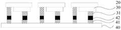
10-刚性基板; 20-柔性转移头;10-rigid substrate; 20-flexible transfer head;
30-微发光二极管芯片; 31-电极;30-micro light-emitting diode chip; 31-electrode;
40-电路基板; 41-电极;40-circuit substrate; 41-electrodes;
42-焊料; 50-临时基板;42-solder; 50-temporary substrate;
51-临时键合胶; 60-衬底。51-temporary bonding glue; 60-substrate.
具体实施方式Detailed ways
为使本发明实施例的目的、技术方案和优点更加清楚,下面将结合本发明实施例中的附图,对本发明实施例中的技术方案进行清楚、完整地描述,显然,所描述的实施例是本发明一部分实施例,而不是全部的实施例。基于本发明中的实施例,本领域普通技术人员在没有做出创造性劳动前提下所获得的所有其他实施例,都属于本发明保护的范围。In order to make the purpose, technical solutions and advantages of the embodiments of the present invention clearer, the technical solutions in the embodiments of the present invention will be clearly and completely described below in conjunction with the drawings in the embodiments of the present invention. Obviously, the described embodiments It is a part of embodiments of the present invention, but not all embodiments. Based on the embodiments of the present invention, all other embodiments obtained by persons of ordinary skill in the art without making creative efforts belong to the protection scope of the present invention.
现阶段Micro LED显示面板的制备,多是先在蓝宝石类的衬底上外延获得MicroLED,随后通过激光剥离(Laser lift-off)技术将微发光二极管芯片从衬底上分离开,然后通过微转印(Micro Transfer Print)技术将微发光二极管芯片转移到已经预先制备完成电极图案的电路基板上,形成Micro LED阵列,最后再经过封装等制程,制得Micro LED显示面板。其中,微转印技术的原理大致为:使用具有一定粘性的转移头(Transfer head),例如聚二甲基硅氧烷(Polydimethylsiloxane,PDMS)转移头拾取微发光二极管芯片,然后将PDMS转移头与电路基板进行对位。电路基板上设有与每个微发光二极管芯片的电极相对应的焊点,焊点表面设有焊料,焊料层在高温下与微发光二极管芯片的电极焊接固定,从而使微发光二极管芯片的电极与电路基板上的电极实现电连接,最后再将PDMS转移头从电路基板上剥离,即可完成微发光二极管芯片的批量转移,形成Micro LED阵列。At present, the preparation of Micro LED display panels is mostly to obtain Micro LED by epitaxy on a sapphire substrate, and then separate the micro LED chip from the substrate by laser lift-off technology, and then use micro-spin Printing (Micro Transfer Print) technology transfers micro light emitting diode chips to circuit substrates that have pre-prepared electrode patterns to form a Micro LED array, and finally undergoes packaging and other processes to produce a Micro LED display panel. Among them, the principle of the micro-transfer printing technology is roughly as follows: use a transfer head with a certain viscosity, such as a polydimethylsiloxane (Polydimethylsiloxane, PDMS) transfer head to pick up the micro-LED chip, and then combine the PDMS transfer head with the The circuit board is aligned. Solder spots corresponding to the electrodes of each micro-light emitting diode chip are provided on the circuit substrate, solder is provided on the surface of the solder spot, and the solder layer is welded and fixed with the electrodes of the micro-light-emitting diode chip at high temperature, so that the electrodes of the micro-light-emitting diode chip It is electrically connected to the electrodes on the circuit substrate, and finally the PDMS transfer head is peeled off from the circuit substrate to complete the batch transfer of micro light-emitting diode chips to form a Micro LED array.
但是,发明人研究发现采用现有技术,在微发光二极管芯片于接受基板进行键合时,由于目前所常采用的转移头的材质较软,无法为微发光二极管芯片提供足够的压合力,导致微发光二极管芯片不能有效地固定在电路基板上,微发光二极管芯片的电极与电路基板上的电极不能实现良好的电连接,使微发光二极管显示面板的品质和良率均下降。为了解决上述问题,发明人提出了一种微发光二极管的转移方法。However, the inventors have found that using the existing technology, when the micro-LED chip is bonded to the receiving substrate, the material of the commonly used transfer head is relatively soft, which cannot provide sufficient pressing force for the micro-light-emitting diode chip, resulting in The micro-LED chip cannot be effectively fixed on the circuit substrate, and the electrodes of the micro-LED chip and the electrodes on the circuit substrate cannot achieve good electrical connection, which reduces the quality and yield of the micro-LED display panel. In order to solve the above problems, the inventors proposed a method for transferring micro light emitting diodes.
实施例一Embodiment one
本实施例提供一种微发光二极管的转移方法,请参考图1并结合图2至图5,具体可包括如下步骤:This embodiment provides a method for transferring micro-light emitting diodes. Please refer to FIG. 1 in combination with FIG. 2 to FIG. 5, which may specifically include the following steps:
S1、采用设置于刚性基板10上的柔性转移头20拾取微发光二极管芯片30;S1, using the
S2、对刚性基板10所拾取的微发光二极管芯片30与电路基板40进行对位,使微发光二极管芯片30上的电极31与电路基板40上的电极41相对应;S2. Align the
S3、对刚性基板10施加压力,使微发光二极管芯片30被挤压入柔性转移头20内,压力经由刚性基板10及柔性转移头20传递给微发光二极管芯片30,并使微发光二极管芯片30上的电极31与电路基板40上的电极41实现键合;S3. Apply pressure to the
S4、使柔性转移头20与微发光二极管芯片30分离。S4 , separating the
本实施例提供的微发光二极管的转移方法,将柔性转移头20设置在刚性基板10上,在将微发光二极管芯片30与电路基板40进行压合时,微发光二极管芯片30会挤压柔性转移头20并不断接近刚性基板10,这样对刚性基板10所施加的压合力能够有效地传递给微发光二极管芯片30以及电路基板40,确保微发光二极管芯片30的电极31与电路基板40上的电极41实现有效的键合及电连接,提高微发光二极管器件的性能。In the micro-LED transfer method provided in this embodiment, the
此外,在压合过程中,由于微发光二极管芯片30会挤压入柔性转移头20内,即柔性转移头20被挤压变形而形成了用于容纳微发光二极管芯片30的凹槽,该凹槽增大了柔性转移头20与微发光二极管芯片30之间的接触面积及粘结力,此外该凹槽还能起到一定的限位作用,所以能够避免微发光二极管芯片30与电路基板40之间发生偏移,进一步确保微发光二极管芯片30与电路基板40之间实现有效键合及电连接。In addition, during the pressing process, since the
并且,该转移方法增加了微发光二极管转印技术的功能性,而且工艺流程较为简单,提高了微发光二极管芯片30的批量转移效率。Moreover, the transfer method increases the functionality of micro-LED transfer technology, and the process flow is relatively simple, which improves the batch transfer efficiency of
本实施例对于微发光二极管芯片30及其电极31的结构不做特别限定,只要在键合时,该微发光二极管芯片30的n型电极和p型电极中至少有一个朝向电路基板40并用于与电路基板40焊接即可。比如该微发光二极管芯片30是倒装芯片,在键合时,其n型电极和p型电极均朝向电路基板40并用于与电路基板40焊接;或者,该微发光二极管芯片30也可以是垂直芯片,在键合时,其n型电极和p型电极中有一个朝向电路基板40并用于与电路基板40连接,另一个背向电路基板40。In this embodiment, the structure of the
为方便说明,图2至图6是倒装芯片为例对本实施例的转移方法进行阐述,但本领域技术人员应当理解,本实施例所提供的微发光二极管的转移方法并不仅限于倒装芯片,其也同样可适用于垂直芯片,只要有至少一个电极31与电路基板40焊接连接即可适用该转移方法。For the convenience of description, Fig. 2 to Fig. 6 illustrate the transfer method of this embodiment with flip chip as an example, but those skilled in the art should understand that the transfer method of micro light emitting diodes provided in this embodiment is not limited to flip chip , which is also applicable to vertical chips, as long as at least one
请进一步参考图1,在采用柔性转移头20拾取微发光二极管芯片30之前,微发光二极管芯片30可以设置于临时基板50上,即设置于刚性基板10上的柔性转移头20从临时基板50上拾取微发光二极管芯片30。Please further refer to FIG. 1 , before using the
请进一步参考图1和图2并结合图6,本实施例提供的微发光二极管的转移方法,在实施步骤S1之前还可以包括如下的步骤S0:Please further refer to FIG. 1 and FIG. 2 in combination with FIG. 6, the method for transferring micro-light emitting diodes provided in this embodiment may also include the following step S0 before implementing step S1:
将形成于衬底60上的微发光二极管芯片30从衬底60转移到临时基板50上。The
本实施例对于衬底60的材质不做特别限定,可根据加工设备和微发光二极管器件的要求合理选择,比如可以是目前微发光二极管器件领域所常用的蓝宝石衬底、碳化硅衬底、硅衬底等。本实施例对于微发光二极管芯片30在衬底60上的形成方式也不做特别限定,比如可通过外延生长在C面蓝宝石衬底上。In this embodiment, the material of the
本实施例对于将微发光二极管芯片30从衬底60转移到临时基板50上的具体实现方式不做特别限定,比如可以采用激光剥离技术,具体如图6所示,可首先采用临时键合胶51将微发光二极管芯片30粘贴到临时基板50上,然后激光剥离去除衬底60,即实现了微发光二极管芯片30从衬底60上转移到临时基板50上。This embodiment does not specifically limit the specific implementation of transferring the
具体的,在采用设置于刚性基板10上的柔性转移头20从临时基板50上拾取微发光二极管芯片30之前,还可以选择进行解键合,比如根据临时键合胶51的材质选择对其进行加热或UV辐照,以降低临时键合胶51与微发光二极管芯片30之间的作用力,方便柔性转移头20从临时基板50上拾取微发光二极管芯片30。或者,若临时键合胶51与微发光二极管芯片30之间的粘结力小于柔性转移头20与微发光二极管芯片30之间的粘结力,也可以不实施解键合的步骤。Specifically, before using the
具体的,在步骤S1中,设置于刚性基板10上的柔性转移头20可以通过范德华力拾取微发光二极管芯片30。Specifically, in step S1 , the
本实施例对于柔性转移头20的材质不做特别限定,其只要与微发光二极管芯片30之间具有足够的粘结力以克服临时键合胶51与微发光二极管芯片30之间的作用力,并能够在压合过程中容易被微发光二极管芯片30挤压变形即可,比如可以是以聚二甲基硅氧烷PDMS作为基础成分的转移头。即该柔性转移头20可以是由PDMS材料制成,也可以通过在PDMS材料中掺杂其它材料以改善其黏度、硬度、耐受温度等理化性质,进而提高PDMS转移头拾取微发光二极管芯片30、微发光二极管芯片30与电路基板40键合、键合后PDMS转移头与微发光二极管芯片30分离的效果。为方便说明,本实施例将以聚二甲基硅氧烷PDMS作为基础成分的转移头统称为PDMS转移头。In this embodiment, the material of the
请进一步参考图1和图3,在步骤S2中,对刚性基板10所拾取的微发光二极管芯片30与电路基板40进行对位,以使微发光二极管芯片30上的电极31与电路基板40上的电极41相向设置并互相对准。Please refer to FIG. 1 and FIG. 3 further. In step S2, the
本实施例中,电路基板40用于承载并驱动微发光二极管芯片30,使微发光二极管芯片30被驱动发光。该电路基板40具体可以是目前微发光二极管显示面板中所常用的电路基板40,包括但不限于印刷背板、TFT背板、PM走线背板、CMOS晶体管背板等。In this embodiment, the
请进一步参考图1和图4,步骤S3中,对刚性基板10施加压力(图4中虚线箭头方向代表压力的方向),由于柔性转移头20的材质较软,所以微发光二极管芯片30相对于刚性基板10朝向背离压力的方向运动并挤压柔性转移头20;随着柔性转移头20不断被挤压变形,微发光二极管芯片30与刚性基板10之间的距离不断缩小甚至无限接近,从而使刚性基板10能够提供压合过程中所需的硬度,确保施加给刚性基板10的压力能够充分地传递给微发光二极管芯片30和电路基板40,也就有利于实现微发光二极管芯片30上的电极31与电路基板40上的电极41之间的键合并形成良好的电连接。Please further refer to Fig. 1 and Fig. 4, in step S3, apply pressure to rigid substrate 10 (the dotted line arrow direction represents the direction of pressure in Fig. The
如前所述,刚性基板10应能够在压合过程中提供足够的硬度,使压合力能够经刚性基板10充分传递给微发光二极管芯片30和电路基板40。该刚性基板10具体可以是硬质玻璃基板、硬质塑料基板或者金属基板,其中硬质玻璃基板比如可以是硼硅玻璃板材,硬质塑料基板比如可以是聚氯乙烯板材、聚氨酯板材等,金属基板比如可以是钢板、铜板等。As mentioned above, the
可以理解,在对刚性基板10施加压力的过程中,由于微发光二极管芯片30被挤压入柔性转移头20内,导致柔性转移头20被挤压变形。直观表现为,柔性转移头20与微发光二极管芯片30直接接触的部位被压缩而厚度减小且向平行于刚性基板10的方向延伸,导致柔性转移头20不与微发光二极管芯片30接触的部位也会随之延伸,且厚度也可能会略有增大。It can be understood that during the process of applying pressure to the
为避免微发光二极管芯片30被厚度增大的柔性转移头20完全包裹而影响与电路基板40之间的键合连接,柔性转移头20的厚度最好不超过微发光二极管芯片30的厚度(或称为高度)。此外,柔性转移头20的厚度还应考虑柔性转移头20自身的黏度、硬度等材料特征,使在键合时,施加给刚性基板10的压合力能够充分传递给微发光二极管芯片30,并确保在拾取过程中,柔性转移头20与微发光二极管芯片30之间具有足够的范德华力,且在键合完成之后,柔性转移头20可较易与微发光二极管芯片30分离。上述因素综合考量,加之当前微发光二极管芯片30的一般厚度为5~7μm,因此可控制柔性转移头20的厚度不超过7μm,比如1~7μm,进一步如3~5μm。In order to avoid the micro light emitting
上述超薄膜厚的柔性转移头20不仅能够避免微发光二极管芯片30被完全包裹,而且在压合过程中,由于柔性转移头20的厚度会在此基础上进一步降低,从而更有利于实现微发光二极管芯片30与刚性基板10之间无限接近,确保压合力经由刚性基板10传递给微发光二极管芯片30及电路基板40。此外,上述厚度的柔性转移头20还容易实现后续步骤S4中与微发光二极管芯片30之间的分离。The ultra-thick
请进一步参考图4,优选的,在微发光二极管芯片30被挤压入柔性转移头20内的过程中,相邻的柔性转移头20之间不互相接触。或者说,相邻柔性转移头20之间具有足够的间距,这样在对刚性基板10施加压力的过程中,虽然柔性转移头20被挤压而向平行于刚性基板10的方向延伸,但柔性转移头20之间仍旧保持间隔设置,避免柔性转移头20为一整层设计或者在压合过程中相邻柔性转移头20互相接触而导致的微发光二极管芯片30与电路基板40之间发生偏移。Please further refer to FIG. 4 , preferably, when the
此外,由于相邻柔性转移头20之间间隔设置,在后续通过焊接、尤其是加热焊接实现微发光二极管芯片30与电路基板40之间的键合时,即使柔性转移头20受热发生膨胀,各柔性转移头20也是以自己所在位置为中心发生膨胀,而避免柔性转移头20为一整层设计或者在压合过程中相邻柔性转移头20互相接触而导致微发光二极管芯片30相对于电路基板40发生整体偏移。In addition, since the adjacent flexible transfer heads 20 are arranged at intervals, when the bonding between the
本实施例对于微发光二极管芯片30与电路基板40之间实现键合的具体方式不做特别限定,如前所述,可通过焊接方式实现。具体的,可事先在电路基板40的电极41上设有焊料42。在压合过程中,焊料42与微发光二极管芯片30的电极31通过焊接实现键合。具体的,在压合过程中,对焊料42进行加热后冷却,使焊料42熔化再凝固,完成微发光二极管芯片30与电路基板40之间的键合。In this embodiment, there is no special limitation on the specific way of realizing the bonding between the
进一步的,在焊料42与微发光二极管芯片30的电极31之间进行焊接时,焊接温度最好不超过柔性转移头20的最高承受温度(或称为最高耐受温度),比避免损伤柔性转移头20,也避免对微发光二极管芯片30造成伤害。具体的,所选用的焊料42为低温焊料,其实际操作时的焊接温度不超过柔性转移头20的最高承受温度。比如目前工业中普遍使用的PDMS转移头的最高承受温度约为120℃,则焊料42可以选择铟、铟锡合金、铋铅锡合金等。以铟例,其熔点约为156.6℃,在实际操作时,在100℃左右焊接铟亦可形成金属键合。而铟锡合金、铋铅锡合金等一般认为其熔点均低于PDMS的最高耐受温度120度。Further, when soldering between the
请进一步参考图1和图5,在完成微发光二极管芯片30与电路基板40之间的键合之后,分离柔性转移头20与微发光二极管芯片30。本实施例对于柔性转移头20与微发光二极管芯片30之间的分离手段不做特别限定,可根据柔性转移头20的具体材质等因素选择适宜的分离手段,比如可首先分离刚性基板10和柔性转移头20,然后将柔性转移头20从微发光二极管芯片30上剥离,或者也可以将刚性基板10和柔性转移头20一起与微发光二极管芯片30实现分离,从而完成微发光二极管芯片30到电路基板40的转移。Please further refer to FIG. 1 and FIG. 5 , after the bonding between the
实施例二Embodiment two
本实施例提供一种微发光二极管的转移方法,如图1、图6和图7所示,该转移方法与实施例一的区别在于:在步骤S1中,采用设置于刚性基板10上的柔性转移头20从临时基板50上选择性拾取微发光二极管芯片30。This embodiment provides a method for transferring micro-light emitting diodes, as shown in Fig. 1, Fig. 6 and Fig. 7. The difference between this transfer method and
不难理解,在实际工业生产中,微发光二极管芯片30在衬底60和电路基板40上的排布方式往往并不相同。前者主要取决于微发光二极管芯片30的形成工艺,后者主要取决于微发光二极管显示面板的像素排布。因此在进行微发光二极管芯片30的批量转移时,柔性转移头20可从临时基板50上选择性拾取柔性转移头20。It is not difficult to understand that in actual industrial production, the arrangements of the micro-LED chips 30 on the
如图7所示,以电路基板40上相邻两个微发光二极管芯片30之间的间距为衬底60上相邻两个微发光二极管芯片30之间的间距的2倍为例,设置于刚性基板10上的柔性转移头20可以先拾取1#微发光二极管芯片30和3#微发光二极管芯片30,然后再拾取2#和4#微发光二极管芯片30。As shown in FIG. 7 , taking the distance between two adjacent micro light emitting diode chips 30 on the
实施例三Embodiment Three
本实施例提供一种显示面板的制作方法,请参考图1至图7,包括:This embodiment provides a method for manufacturing a display panel, please refer to FIG. 1 to FIG. 7, including:
在衬底60上形成微发光二极管芯片30;Forming the micro light emitting
按照实施例一或实施例二中的转移方法,将微发光二极管芯片30转移到电路基板40上,形成用于构成显示的微发光二极管显示阵列;According to the transfer method in
对微发光二极管显示阵列进行封装,得到微发光二极管显示面板。The micro light emitting diode display array is packaged to obtain a micro light emitting diode display panel.
如前述,本实施例对于衬底60的材质不做特别限定,包括但不限于蓝宝石衬底、碳化硅衬底、硅衬底。本实施例对于微发光二极管芯片30的形成方式也不做特别限定,比如可以在C面蓝宝石衬底上通过外延生长而形成微发光二极管芯片30。As mentioned above, this embodiment does not specifically limit the material of the
本实施例对于微发光二极管芯片30的结构也不做特别限定,比如目前典型的GaN基Micro LED芯片结构,包括位于衬底60上的n-GaN层、位于一部分n-GaN层上的n型电极、位于另一部分n-GaN层上的多量子阱有源层、位于多量子阱有源层上的p-GaN层、位于p-GaN层上的p型电极。本实施例中,为方便说明,将n型电极和p型电极统称为电极31。This embodiment does not specifically limit the structure of the micro light-emitting
本实施例对于微发光二极管显示阵列的封装方式不做特别限定,比如可采取物理沉积制程,完成保护层与上电极,从而完成封装,得到微发光二极管显示面板。In this embodiment, the packaging method of the micro-LED display array is not particularly limited. For example, a physical deposition process can be adopted to complete the protective layer and the upper electrode, thereby completing the packaging and obtaining the micro-LED display panel.
本实施例提供的显示面板的制作方法,由于包括前述实施例一中的转移方法,形成用于构成显示的微发光二极管显示阵列,因此也具有与实施例一相同的优势,由于微发光二极管芯片30的电极31与电路基板40上的电极41之间形成了有效的键合及电连接,因此该微发光二极管显示面板的性能和良率都有明显提升。The manufacturing method of the display panel provided by this embodiment includes the transfer method in the first embodiment to form a micro-light-emitting diode display array for display, so it also has the same advantages as the first embodiment, because the micro-light-emitting diode chip Effective bonding and electrical connection are formed between the
最后应说明的是:以上各实施例仅用以说明本发明的技术方案,而非对其限制;尽管参照前述各实施例对本发明进行了详细的说明,本领域的普通技术人员应当理解:其依然可以对前述各实施例所记载的技术方案进行修改,或者对其中部分或者全部技术特征进行等同替换;而这些修改或者替换,并不使相应技术方案的本质脱离本发明各实施例技术方案的范围。Finally, it should be noted that: the above embodiments are only used to illustrate the technical solutions of the present invention, rather than limiting them; although the present invention has been described in detail with reference to the foregoing embodiments, those of ordinary skill in the art should understand that: It is still possible to modify the technical solutions described in the foregoing embodiments, or perform equivalent replacements for some or all of the technical features; and these modifications or replacements do not make the essence of the corresponding technical solutions deviate from the technical solutions of the various embodiments of the present invention. scope.
Claims (3)
Priority Applications (3)
| Application Number | Priority Date | Filing Date | Title |
|---|---|---|---|
| CN201910470274.XACN112018218B (en) | 2019-05-31 | 2019-05-31 | Micro light emitting diode transfer method and display panel manufacturing method |
| KR1020217035346AKR102762767B1 (en) | 2019-05-31 | 2019-11-26 | Method for transferring micro light-emitting diodes and method for manufacturing display panels |
| PCT/CN2019/120948WO2020238099A1 (en) | 2019-05-31 | 2019-11-26 | Method for transferring micro light-emitting diode and method for manufacturing display panel |
Applications Claiming Priority (1)
| Application Number | Priority Date | Filing Date | Title |
|---|---|---|---|
| CN201910470274.XACN112018218B (en) | 2019-05-31 | 2019-05-31 | Micro light emitting diode transfer method and display panel manufacturing method |
Publications (2)
| Publication Number | Publication Date |
|---|---|
| CN112018218A CN112018218A (en) | 2020-12-01 |
| CN112018218Btrue CN112018218B (en) | 2023-02-28 |
Family
ID=73502080
Family Applications (1)
| Application Number | Title | Priority Date | Filing Date |
|---|---|---|---|
| CN201910470274.XAActiveCN112018218B (en) | 2019-05-31 | 2019-05-31 | Micro light emitting diode transfer method and display panel manufacturing method |
Country Status (3)
| Country | Link |
|---|---|
| KR (1) | KR102762767B1 (en) |
| CN (1) | CN112018218B (en) |
| WO (1) | WO2020238099A1 (en) |
Families Citing this family (16)
| Publication number | Priority date | Publication date | Assignee | Title |
|---|---|---|---|---|
| CN112582520B (en)* | 2020-12-29 | 2021-10-08 | 苏州芯聚半导体有限公司 | Micro-LED transfer method and display panel |
| CN113035763B (en)* | 2021-03-01 | 2023-06-09 | 东莞市中麒光电技术有限公司 | High-precision chip transfer method |
| CN113078145B (en)* | 2021-03-30 | 2022-06-21 | 厦门乾照半导体科技有限公司 | Array type light emitting diode device and manufacturing method thereof |
| CN113257979A (en)* | 2021-05-12 | 2021-08-13 | 华南理工大学 | Chip transfer substrate, chip transfer apparatus and chip transfer method |
| CN114038870A (en)* | 2021-05-18 | 2022-02-11 | 重庆康佳光电技术研究院有限公司 | Chip transfer method, display back plate and display device |
| CN113284991A (en)* | 2021-07-09 | 2021-08-20 | 苏州芯聚半导体有限公司 | Micro LED chip, packaging method thereof and electronic device |
| CN113675323B (en)* | 2021-08-13 | 2025-03-07 | 乙力国际股份有限公司 | A micro LED chip and control substrate eutectic structure and preparation method thereof |
| CN113764546A (en)* | 2021-08-30 | 2021-12-07 | 东莞市中麒光电技术有限公司 | Mini-LED device, LED display module and manufacturing method thereof |
| CN116264239A (en)* | 2021-12-15 | 2023-06-16 | 厦门市芯颖显示科技有限公司 | micro-LED display module, manufacturing method thereof and display panel |
| CN113990765B (en)* | 2021-12-28 | 2023-04-18 | 深圳市思坦科技有限公司 | Preparation method of flexible light-emitting device, flexible light-emitting device and light-emitting device |
| CN114664996B (en)* | 2022-03-11 | 2025-09-09 | 京东方科技集团股份有限公司 | Repairing method, repairing device and repairing system for display panel |
| CN114725082B (en)* | 2022-03-29 | 2024-07-26 | 厦门天马微电子有限公司 | Display panel, display device and light emitting diode transfer device |
| CN114783911B (en)* | 2022-04-02 | 2024-07-23 | 深圳市华星光电半导体显示技术有限公司 | LED chip transfer device, chip assembly process and display screen preparation method |
| CN115241113A (en)* | 2022-06-24 | 2022-10-25 | 佛山市国星光电股份有限公司 | A chip transfer device |
| CN115083990A (en)* | 2022-07-19 | 2022-09-20 | 南京大学 | Micro-LED Mass Transfer Method |
| CN116944759A (en)* | 2023-09-20 | 2023-10-27 | 武汉高芯科技有限公司 | Flip-chip bonding processing method with low contact resistance and flip-chip interconnection structure |
Citations (4)
| Publication number | Priority date | Publication date | Assignee | Title |
|---|---|---|---|---|
| US8349116B1 (en)* | 2011-11-18 | 2013-01-08 | LuxVue Technology Corporation | Micro device transfer head heater assembly and method of transferring a micro device |
| CN207116403U (en)* | 2017-04-21 | 2018-03-16 | 厦门市三安光电科技有限公司 | A kind of transposition head for microcomponent transfer |
| CN108258006A (en)* | 2017-12-21 | 2018-07-06 | 厦门市三安光电科技有限公司 | micro light emitting element |
| CN108463891A (en)* | 2016-01-20 | 2018-08-28 | 歌尔股份有限公司 | Micro- light emitting diode transfer method and manufacturing method |
Family Cites Families (8)
| Publication number | Priority date | Publication date | Assignee | Title |
|---|---|---|---|---|
| JP6490522B2 (en) | 2015-07-14 | 2019-03-27 | 東レエンジニアリング株式会社 | Semiconductor mounting equipment |
| KR101793542B1 (en) | 2016-08-26 | 2017-11-03 | 엘지전자 주식회사 | Transfer head of the semiconductor light emitting device, transfer system and method for transferring the semiconductor light emitting device |
| KR102402189B1 (en)* | 2015-08-26 | 2022-05-25 | 엘지전자 주식회사 | Transfer unit for micro device |
| WO2017037475A1 (en)* | 2015-09-02 | 2017-03-09 | Oculus Vr, Llc | Assembly of semiconductor devices |
| JP2017216312A (en) | 2016-05-31 | 2017-12-07 | パナソニックIpマネジメント株式会社 | Electronic component mounting method |
| US10290785B2 (en)* | 2017-10-03 | 2019-05-14 | Center For Integrated Smart Sensors Foundation | Laminating structure of electronic device using transferring element, transferring apparatus for fabricating the electronic device and method for fabricating the electronic device |
| CN107644927B (en)* | 2017-10-20 | 2020-01-31 | 上海天马微电子有限公司 | Micro light-emitting diode growth and transfer equipment and transfer method |
| CN107799455B (en)* | 2017-10-24 | 2020-06-19 | 上海天马微电子有限公司 | Transfer head, manufacturing method thereof, transfer printing method and manufacturing method of display panel |
- 2019
- 2019-05-31CNCN201910470274.XApatent/CN112018218B/enactiveActive
- 2019-11-26KRKR1020217035346Apatent/KR102762767B1/enactiveActive
- 2019-11-26WOPCT/CN2019/120948patent/WO2020238099A1/ennot_activeCeased
Patent Citations (4)
| Publication number | Priority date | Publication date | Assignee | Title |
|---|---|---|---|---|
| US8349116B1 (en)* | 2011-11-18 | 2013-01-08 | LuxVue Technology Corporation | Micro device transfer head heater assembly and method of transferring a micro device |
| CN108463891A (en)* | 2016-01-20 | 2018-08-28 | 歌尔股份有限公司 | Micro- light emitting diode transfer method and manufacturing method |
| CN207116403U (en)* | 2017-04-21 | 2018-03-16 | 厦门市三安光电科技有限公司 | A kind of transposition head for microcomponent transfer |
| CN108258006A (en)* | 2017-12-21 | 2018-07-06 | 厦门市三安光电科技有限公司 | micro light emitting element |
Also Published As
| Publication number | Publication date |
|---|---|
| KR102762767B1 (en) | 2025-02-05 |
| WO2020238099A1 (en) | 2020-12-03 |
| CN112018218A (en) | 2020-12-01 |
| KR20210137219A (en) | 2021-11-17 |
Similar Documents
| Publication | Publication Date | Title |
|---|---|---|
| CN112018218B (en) | Micro light emitting diode transfer method and display panel manufacturing method | |
| TWI653694B (en) | Micro light-emitting element array manufacturing method, transfer carrier plate and micro light-emitting element array | |
| CN107431107B (en) | Transfer method, manufacturing method, apparatus and electronic device of micro-light emitting diode | |
| CN105518888B (en) | Restorative procedure, manufacturing method, device and the electronic equipment of micro- light emitting diode | |
| US10367117B2 (en) | Apparatus and method for transferring micro light-emitting diodes | |
| KR101614370B1 (en) | Semiconductor light emitting device, transfer head of the semiconductor light emitting device, and method for transferring the semiconductor light emitting device | |
| US11955506B2 (en) | Fabrication method of display device | |
| CN110190014A (en) | A transfer method of Micro-LED | |
| CN109920885B (en) | A method for mass transfer and color transformation of MicroLED | |
| US11705349B2 (en) | Transfer substrate for component transferring and micro LEDs carrying substrate | |
| CN105493297A (en) | Transfer method and manufacturing method and apparatus of micro light emiting diode, and electronic equipment | |
| KR101793542B1 (en) | Transfer head of the semiconductor light emitting device, transfer system and method for transferring the semiconductor light emitting device | |
| KR20180120527A (en) | Method for manufacturing display device using semiconductor light emitting device | |
| CN114141930A (en) | Light emitting diode transfer method, light emitting substrate and display panel | |
| US20120149138A1 (en) | Method for Manufacturing Heat Dissipation Bulk of Semiconductor Device | |
| KR101777610B1 (en) | Transfer head of the semiconductor light emitting device, and method for transferring the semiconductor light emitting device | |
| KR101387847B1 (en) | Method for tranferring and manufacturing flexible light emitting diode using rollers and flexible lexible light emitting diode manufactured by the same | |
| TWI810025B (en) | Ultra-small led chip rework apparatus using transfer method and rework method thereof | |
| CN222365601U (en) | LED array device based on vertical structure LED | |
| CN220753393U (en) | Light emitting element transfer device and transfer component manufacturing device | |
| US20250287736A1 (en) | Led wafer, carrier substrate for led chip, manufacturing method for display device, and repair method for display device | |
| KR20250105744A (en) | Transfer method for light emitting device | |
| TWI861630B (en) | Display device and manufacturing method thereof | |
| TWI830256B (en) | Transfer method of led chip | |
| US20240105759A1 (en) | Apparatus and method for fabricating display panel |
Legal Events
| Date | Code | Title | Description |
|---|---|---|---|
| PB01 | Publication | ||
| PB01 | Publication | ||
| SE01 | Entry into force of request for substantive examination | ||
| SE01 | Entry into force of request for substantive examination | ||
| TA01 | Transfer of patent application right | ||
| TA01 | Transfer of patent application right | Effective date of registration:20201214 Address after:No.146 Tianying Road, high tech Zone, Chengdu, Sichuan Province Applicant after:Chengdu CHENXIAN photoelectric Co.,Ltd. Address before:065500 new industrial demonstration area of Guan County, Langfang, Hebei Applicant before:Yungu (Gu'an) Technology Co.,Ltd. | |
| GR01 | Patent grant | ||
| GR01 | Patent grant |