CN112018143A - Micro light-emitting diode display substrate, display panel, manufacturing method thereof, and display device - Google Patents
Micro light-emitting diode display substrate, display panel, manufacturing method thereof, and display deviceDownload PDFInfo
- Publication number
- CN112018143A CN112018143ACN201910452788.2ACN201910452788ACN112018143ACN 112018143 ACN112018143 ACN 112018143ACN 201910452788 ACN201910452788 ACN 201910452788ACN 112018143 ACN112018143 ACN 112018143A
- Authority
- CN
- China
- Prior art keywords
- substrate
- led
- layer
- micro
- led device
- Prior art date
- Legal status (The legal status is an assumption and is not a legal conclusion. Google has not performed a legal analysis and makes no representation as to the accuracy of the status listed.)
- Pending
Links
- 239000000758substrateSubstances0.000titleclaimsabstractdescription237
- 238000004519manufacturing processMethods0.000titleclaimsabstractdescription24
- 238000000034methodMethods0.000claimsabstractdescription38
- 230000000149penetrating effectEffects0.000claimsabstractdescription7
- 239000010410layerSubstances0.000claimsdescription237
- 238000002955isolationMethods0.000claimsdescription25
- 239000012790adhesive layerSubstances0.000claimsdescription15
- 230000008569processEffects0.000abstractdescription29
- 239000004065semiconductorSubstances0.000description57
- 239000000463materialSubstances0.000description26
- 239000011810insulating materialSubstances0.000description11
- VYPSYNLAJGMNEJ-UHFFFAOYSA-NSilicium dioxideChemical compoundO=[Si]=OVYPSYNLAJGMNEJ-UHFFFAOYSA-N0.000description10
- 239000012535impuritySubstances0.000description10
- 239000000047productSubstances0.000description10
- 229910052814silicon oxideInorganic materials0.000description10
- 239000007772electrode materialSubstances0.000description9
- 238000003892spreadingMethods0.000description9
- 230000007480spreadingEffects0.000description9
- 239000000853adhesiveSubstances0.000description7
- 230000001070adhesive effectEffects0.000description7
- 239000010408filmSubstances0.000description7
- 229910002601GaNInorganic materials0.000description6
- XUIMIQQOPSSXEZ-UHFFFAOYSA-NSiliconChemical compound[Si]XUIMIQQOPSSXEZ-UHFFFAOYSA-N0.000description6
- 229910052710siliconInorganic materials0.000description6
- 239000010703siliconSubstances0.000description6
- 235000012431wafersNutrition0.000description6
- 239000004020conductorSubstances0.000description5
- 238000005516engineering processMethods0.000description5
- 239000000126substanceSubstances0.000description5
- 238000000231atomic layer depositionMethods0.000description4
- 238000005229chemical vapour depositionMethods0.000description4
- 229910052751metalInorganic materials0.000description4
- RYGMFSIKBFXOCR-UHFFFAOYSA-NCopperChemical compound[Cu]RYGMFSIKBFXOCR-UHFFFAOYSA-N0.000description3
- 229910052581Si3N4Inorganic materials0.000description3
- 229910052802copperInorganic materials0.000description3
- 239000010949copperSubstances0.000description3
- 239000013078crystalSubstances0.000description3
- 238000001312dry etchingMethods0.000description3
- 230000000694effectsEffects0.000description3
- 238000005530etchingMethods0.000description3
- 238000000227grindingMethods0.000description3
- 239000002184metalSubstances0.000description3
- 238000000206photolithographyMethods0.000description3
- HQVNEWCFYHHQES-UHFFFAOYSA-Nsilicon nitrideChemical compoundN12[Si]34N5[Si]62N3[Si]51N64HQVNEWCFYHHQES-UHFFFAOYSA-N0.000description3
- JMASRVWKEDWRBT-UHFFFAOYSA-NGallium nitrideChemical compound[Ga]#NJMASRVWKEDWRBT-UHFFFAOYSA-N0.000description2
- 229910052782aluminiumInorganic materials0.000description2
- XAGFODPZIPBFFR-UHFFFAOYSA-NaluminiumChemical compound[Al]XAGFODPZIPBFFR-UHFFFAOYSA-N0.000description2
- 230000004888barrier functionEffects0.000description2
- 230000007547defectEffects0.000description2
- 238000000605extractionMethods0.000description2
- 230000020169heat generationEffects0.000description2
- 230000006872improvementEffects0.000description2
- AMGQUBHHOARCQH-UHFFFAOYSA-Nindium;oxotinChemical compound[In].[Sn]=OAMGQUBHHOARCQH-UHFFFAOYSA-N0.000description2
- 239000012212insulatorSubstances0.000description2
- 238000001755magnetron sputter depositionMethods0.000description2
- 238000000059patterningMethods0.000description2
- 238000005498polishingMethods0.000description2
- 229910052594sapphireInorganic materials0.000description2
- 239000010980sapphireSubstances0.000description2
- 238000000926separation methodMethods0.000description2
- 238000004544sputter depositionMethods0.000description2
- 229910052715tantalumInorganic materials0.000description2
- WFKWXMTUELFFGS-UHFFFAOYSA-NtungstenChemical compound[W]WFKWXMTUELFFGS-UHFFFAOYSA-N0.000description2
- 229910052721tungstenInorganic materials0.000description2
- 239000010937tungstenSubstances0.000description2
- FYYHWMGAXLPEAU-UHFFFAOYSA-NMagnesiumChemical compound[Mg]FYYHWMGAXLPEAU-UHFFFAOYSA-N0.000description1
- 230000009286beneficial effectEffects0.000description1
- 230000015572biosynthetic processEffects0.000description1
- 238000005520cutting processMethods0.000description1
- 238000000708deep reactive-ion etchingMethods0.000description1
- 239000002019doping agentSubstances0.000description1
- 238000000407epitaxyMethods0.000description1
- 238000011049fillingMethods0.000description1
- 239000012467final productSubstances0.000description1
- 229910052738indiumInorganic materials0.000description1
- APFVFJFRJDLVQX-UHFFFAOYSA-Nindium atomChemical compound[In]APFVFJFRJDLVQX-UHFFFAOYSA-N0.000description1
- 229910010272inorganic materialInorganic materials0.000description1
- 239000011147inorganic materialSubstances0.000description1
- 238000011068loading methodMethods0.000description1
- 229910052749magnesiumInorganic materials0.000description1
- 239000011777magnesiumSubstances0.000description1
- 239000007769metal materialSubstances0.000description1
- 238000012986modificationMethods0.000description1
- 230000004048modificationEffects0.000description1
- 238000007517polishing processMethods0.000description1
- 239000002096quantum dotSubstances0.000description1
- 230000006798recombinationEffects0.000description1
- 238000005215recombinationMethods0.000description1
- HBMJWWWQQXIZIP-UHFFFAOYSA-Nsilicon carbideChemical compound[Si+]#[C-]HBMJWWWQQXIZIP-UHFFFAOYSA-N0.000description1
- 229910010271silicon carbideInorganic materials0.000description1
- 239000002356single layerSubstances0.000description1
- 230000002269spontaneous effectEffects0.000description1
- 238000000992sputter etchingMethods0.000description1
- 239000010409thin filmSubstances0.000description1
- 238000010023transfer printingMethods0.000description1
- 238000002834transmittanceMethods0.000description1
- 238000007740vapor depositionMethods0.000description1
- 238000001039wet etchingMethods0.000description1
Images


Classifications
- H—ELECTRICITY
- H10—SEMICONDUCTOR DEVICES; ELECTRIC SOLID-STATE DEVICES NOT OTHERWISE PROVIDED FOR
- H10H—INORGANIC LIGHT-EMITTING SEMICONDUCTOR DEVICES HAVING POTENTIAL BARRIERS
- H10H29/00—Integrated devices, or assemblies of multiple devices, comprising at least one light-emitting semiconductor element covered by group H10H20/00
- H10H29/10—Integrated devices comprising at least one light-emitting semiconductor component covered by group H10H20/00
- H10H29/14—Integrated devices comprising at least one light-emitting semiconductor component covered by group H10H20/00 comprising multiple light-emitting semiconductor components
- H10H29/142—Two-dimensional arrangements, e.g. asymmetric LED layout
- H—ELECTRICITY
- H10—SEMICONDUCTOR DEVICES; ELECTRIC SOLID-STATE DEVICES NOT OTHERWISE PROVIDED FOR
- H10H—INORGANIC LIGHT-EMITTING SEMICONDUCTOR DEVICES HAVING POTENTIAL BARRIERS
- H10H20/00—Individual inorganic light-emitting semiconductor devices having potential barriers, e.g. light-emitting diodes [LED]
- H10H20/80—Constructional details
- H10H20/85—Packages
- H10H20/857—Interconnections, e.g. lead-frames, bond wires or solder balls
Landscapes
- Devices For Indicating Variable Information By Combining Individual Elements (AREA)
- Led Device Packages (AREA)
Abstract
Translated fromChinese
Description
Translated fromChinese技术领域technical field
本申请涉及显示技术领域,特别是涉及一种微发光二极管显示基板、显示面板及其制作方法、显示装置。The present application relates to the field of display technology, and in particular, to a micro-light emitting diode display substrate, a display panel, a manufacturing method thereof, and a display device.
背景技术Background technique
Micro LED(Micro Light Emitting Diode,微发光二极管),是将LED器件微缩化和矩阵化的技术。具体是在一个芯片上集成高密度微小尺寸的LED器件阵列,其中每一LED器件可定址、单独驱动点亮,能够将相邻两个LED器件的像素点距离从毫米降低至微米级,提高显示效果。Micro LED (Micro Light Emitting Diode) is a technology for miniaturizing and matrixing LED devices. Specifically, a high-density and tiny-sized LED device array is integrated on one chip, in which each LED device can be addressed and individually driven to light up, which can reduce the pixel distance between two adjacent LED devices from millimeters to micrometers. Effect.
目前,Micro LED显示面板的制作方法通常是分别制作Micro LED和控制电路基板,然后通过转印的方式将Micro LED转移至控制电路基板上,再进行电连接。在将MicroLED转移至控制电路基板上之前,需要将Micro LED的衬底剥离,但现有技术中衬底剥离工艺较为复杂,使Micro LED显示面板的转移和制作工艺的难度增大。At present, the manufacturing method of the Micro LED display panel is usually to separately manufacture the Micro LED and the control circuit substrate, and then transfer the Micro LED to the control circuit substrate by transfer printing, and then perform electrical connection. Before transferring the Micro LED to the control circuit substrate, the substrate of the Micro LED needs to be peeled off, but the substrate peeling process in the prior art is relatively complicated, which increases the difficulty of the transfer and manufacturing process of the Micro LED display panel.
发明内容SUMMARY OF THE INVENTION
基于此,有必要针对传统的Micro LED衬底剥离工艺复杂的问题,提供一种改善上述问题的微发光二极管显示基板、显示面板及其制作方法、显示装置。Based on this, it is necessary to provide a micro light emitting diode display substrate, a display panel, a method for manufacturing the same, and a display device that improve the above-mentioned problems in order to solve the problem of the complex stripping process of the traditional Micro LED substrate.
根据本申请的一个方面,提供一种微发光二极管显示基板,包括:According to one aspect of the present application, there is provided a micro light emitting diode display substrate, comprising:
衬底层;substrate layer;
多个LED器件,所述多个LED器件彼此绝缘间隔地设于所述衬底层上;以及a plurality of LED devices, the plurality of LED devices are provided on the substrate layer in an insulating space from each other; and
多个连接电极,所述衬底层被构造为具有多个贯穿所述衬底层以暴露所述LED器件部分表面的接触孔,每一所述连接电极用于借助于对应的所述接触孔连接所述LED器件和驱动基板。A plurality of connection electrodes, the substrate layer is configured to have a plurality of contact holes penetrating the substrate layer to expose a part of the surface of the LED device, each of the connection electrodes is used to connect all the connection electrodes by means of the corresponding contact holes. The LED device and the drive substrate are described.
上述微发光二极管显示基板,在衬底层上形成接触孔,并设有用于连接LED器件与驱动基板的连接电极,从而在完成LED器件外延结构的生长后,不需要衬底层剥离,而直接将该微发光二极管显示基板与驱动基板对位键合,即可实现LED器件和驱动基板的连接。一方面相比现有技术中的在完成LED器件制作之后在转移之前需要将衬底层剥离的工艺,降低了工艺难度,提高了产品的生产效率。另一方面,避免在衬底剥离过程中造成LED器件遭到破坏,提高了产品的良率。The above-mentioned micro light-emitting diode display substrate has contact holes formed on the substrate layer, and is provided with connecting electrodes for connecting the LED device and the driving substrate, so that after the growth of the epitaxial structure of the LED device is completed, the substrate layer does not need to be peeled off, and the The micro-light emitting diode display substrate and the driving substrate are aligned and bonded to realize the connection between the LED device and the driving substrate. On the one hand, compared with the prior art process in which the substrate layer needs to be peeled off before the transfer after the LED device is fabricated, the process difficulty is reduced and the production efficiency of the product is improved. On the other hand, the LED device is prevented from being damaged in the process of substrate peeling, and the yield of the product is improved.
在一实施例中,所述微发光二极管显示基板还包括绝缘层;In one embodiment, the micro-LED display substrate further includes an insulating layer;
所述绝缘层覆盖所述接触孔的内壁,且所述绝缘层位于所述连接电极和所述接触孔内壁之间。The insulating layer covers the inner wall of the contact hole, and the insulating layer is located between the connection electrode and the inner wall of the contact hole.
在一实施例中,所述微发光二极管显示基板还包括导电粘附层;In one embodiment, the micro-LED display substrate further includes a conductive adhesive layer;
所述导电粘附层覆盖所述绝缘层和所述LED器件表面对应于所述接触孔的区域,且所述导电粘附层包覆所述连接电极的沿周向的表面和所述连接电极靠近所述LED器件的一端端面。The conductive adhesive layer covers the insulating layer and the area of the surface of the LED device corresponding to the contact hole, and the conductive adhesive layer covers the circumferential surface of the connection electrode and the connection electrode Close to one end face of the LED device.
在一实施例中,所述连接电极远离所述LED器件的一端凸伸出所述接触孔,形成第一凸起部。In one embodiment, one end of the connection electrode away from the LED device protrudes out of the contact hole to form a first protrusion.
在一实施例中,所述微发光二极管显示基板还包括缓冲层;In one embodiment, the micro-LED display substrate further includes a buffer layer;
所述缓冲层形成于所述衬底层与所述LED器件之间;the buffer layer is formed between the substrate layer and the LED device;
所述接触孔贯穿所述衬底层及所述缓冲层。The contact hole penetrates through the substrate layer and the buffer layer.
在一实施例中,所述微发光二极管显示基板还包括隔离结构;In one embodiment, the micro-LED display substrate further includes an isolation structure;
所述隔离结构设于所述衬底层靠近所述LED器件的一侧,且位于多个LED器件之间,所述隔离结构用于将相邻的所述LED器件绝缘隔离。The isolation structure is disposed on a side of the substrate layer close to the LED device, and is located between a plurality of LED devices, and the isolation structure is used for insulating and isolating adjacent LED devices.
根据本申请另一方面,提供一种显示面板,包括驱动基板及键合于所述驱动基板一侧的微发光二极管显示基板;According to another aspect of the present application, a display panel is provided, comprising a driving substrate and a micro-LED display substrate bonded to one side of the driving substrate;
其中,所述微发光二极管显示基板为如上述实施例中的微发光二极管显示基板;每一所述连接电极借助于对应的所述接触孔连接所述LED器件和所述驱动基板。Wherein, the micro light emitting diode display substrate is the micro light emitting diode display substrate in the above-mentioned embodiment; each of the connecting electrodes is connected to the LED device and the driving substrate by means of the corresponding contact hole.
在一实施例中,所述连接电极远离所述LED器件的一端凸伸出所述接触孔,形成第一凸起部;In one embodiment, one end of the connection electrode away from the LED device protrudes out of the contact hole to form a first protrusion;
所述驱动基板上设有与所述第一凸起部相配的第二凸起部。The driving substrate is provided with a second protruding portion matched with the first protruding portion.
一种显示装置,包括上述实施例中的显示面板。A display device includes the display panel in the above embodiments.
根据本申请又一方面,提供一种显示面板的制作方法,包括以下步骤:According to yet another aspect of the present application, a method for manufacturing a display panel is provided, comprising the following steps:
提供一微发光二极管显示基板;所述微发光二极管显示基板包括衬底层、多个LED器件和多个连接电极,所述多个LED器件彼此绝缘间隔地设于所述衬底层上,所述衬底层被构造为具有多个贯穿所述衬底层以暴露所述LED器件部分表面的接触孔,所述连接电极用于借助于对应的所述接触孔连接所述LED器件和驱动基板;A micro-LED display substrate is provided; the micro-LED display substrate includes a substrate layer, a plurality of LED devices and a plurality of connection electrodes, the plurality of LED devices are provided on the substrate layer in an insulating interval from each other, and the substrate the bottom layer is configured to have a plurality of contact holes penetrating through the substrate layer to expose part of the surface of the LED device, and the connection electrodes are used for connecting the LED device and the driving substrate by means of the corresponding contact holes;
将所述发光二极管显示基板与驱动基板对位键合。The light emitting diode display substrate and the driving substrate are aligned and bonded.
上述的显示面板的制作方法,在衬底层上形成接触孔,并设有用于连接LED器件与驱动基板的连接电极,从而在完成LED器件外延结构的生长后,不需要衬底层剥离,而直接将该微发光二极管显示基板与驱动基板对位键合,即可实现LED器件和驱动基板的连接。一方面相比现有技术中的在完成LED器件制作之后在转移之前需要将衬底层剥离的工艺,降低了工艺难度,提高了产品的生产效率。另一方面,避免在衬底剥离过程中造成LED器件遭到破坏,提高了产品的良率。The above-mentioned manufacturing method of the display panel forms a contact hole on the substrate layer, and is provided with a connecting electrode for connecting the LED device and the driving substrate, so that after the growth of the epitaxial structure of the LED device is completed, the substrate layer does not need to be peeled off, and the substrate layer is directly removed. The micro-light emitting diode display substrate and the driving substrate are aligned and bonded, so that the connection between the LED device and the driving substrate can be realized. On the one hand, compared with the prior art process in which the substrate layer needs to be peeled off before the transfer after the LED device is fabricated, the process difficulty is reduced and the production efficiency of the product is improved. On the other hand, the LED device is prevented from being damaged in the process of substrate peeling, and the yield of the product is improved.
附图说明Description of drawings
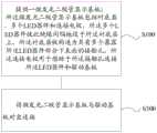
图1为本申请一实施例中的显示面板的截面示意图;FIG. 1 is a schematic cross-sectional view of a display panel according to an embodiment of the application;
图2为本申请一实施例中的显示面板的制作方法的流程示意图;FIG. 2 is a schematic flowchart of a manufacturing method of a display panel according to an embodiment of the present application;
图3~图16示出了本申请一实施例中的显示面板的制作方法对应步骤中的显示面板的截面示意图。3 to 16 are schematic cross-sectional views of the display panel in corresponding steps of the manufacturing method of the display panel according to an embodiment of the present application.
具体实施方式Detailed ways
为了便于理解本申请,下面将参照相关附图对本申请进行更全面的描述。附图中给出了本申请的较佳的实施例。但是,本申请可以以许多不同的形式来实现,并不限于本文所描述的实施例。相反地,提供这些实施例的目的是使对本申请的公开内容的理解更加透彻全面。In order to facilitate understanding of the present application, the present application will be described more fully below with reference to the related drawings. The preferred embodiments of the present application are shown in the accompanying drawings. However, the application may be implemented in many different forms and is not limited to the embodiments described herein. Rather, these embodiments are provided so that a thorough and complete understanding of the disclosure of this application is provided.
在说明书中,短语“平面示意图”是指当从上方观察目标部分时的附图,短语“截面示意图”是指从侧面观察通过竖直地切割目标部分截取的剖面时的附图。In the specification, the phrase "schematic plan view" refers to the drawing when the target portion is viewed from above, and the phrase "schematic cross-sectional view" refers to the drawing when a cross section taken by vertically cutting the target portion is viewed from the side.
此外,附图并不是1:1的比例绘制,并且各元件的相对尺寸在附图中仅以示例地绘制,而不一定按照真实比例绘制。Furthermore, the figures are not drawn to a 1:1 scale and the relative dimensions of elements in the figures are drawn by way of example only and not necessarily to true scale.
正如背景技术所述,Micro LED是将LED结构进行薄膜化、微小化、阵列化的技术。现有的Micro LED显示面板一般是通过平面结构(包含正装和倒装)或垂直结构将LED器件与驱动基板连接在一起。其中,平面结构的Micro LED器件的P、N电极在同一侧,导致电流拥挤,发热量高。垂直结构的Micro LED器件首先需要在衬底(例如蓝宝石衬底)上生长形成磊晶膜结构,再将衬底剥离后,转移至驱动基板上。As mentioned in the background art, Micro LED is a technology for thinning, miniaturizing, and arraying LED structures. Existing Micro LED display panels generally connect LED devices and driving substrates together through a planar structure (including front-loading and flip-chipping) or a vertical structure. Among them, the P and N electrodes of the flat-structured Micro LED device are on the same side, resulting in current crowding and high heat generation. Micro LED devices with a vertical structure first need to grow on a substrate (such as a sapphire substrate) to form an epitaxial film structure, and then peel off the substrate and transfer it to a driving substrate.
针对平面结构的LED器件,由于电流拥挤、发热量高,影响LED器件的使用寿命。针对垂直结构的LED器件,受限于剥离工艺的复杂度,在衬底剥离中容易造成衬底之上的结构发生破坏。尤其在一些实施方式中,对于RGB三色彩色显示的显示面板而言,用于形成R、G、B三种颜色的LED器件所需要的材料不同,其需要在不同的晶圆上生长以形成不同的外延结构,再分别转移至驱动基板上。不同材料制成的LED器件需要单独制作,且分别剥离衬底,进一步地增加了Micro LED显示面板的制作和转移工艺,阻碍了量产的效率的提高以及产品良率的提高。For LED devices with a planar structure, due to current crowding and high heat generation, the service life of the LED devices is affected. For LED devices with vertical structures, due to the complexity of the lift-off process, it is easy to cause damage to the structure above the substrate during substrate lift-off. Especially in some embodiments, for the RGB three-color display panel, the materials required for forming the three-color LED devices of R, G, and B are different, which need to be grown on different wafers to form Different epitaxial structures are then transferred to the driving substrate respectively. LED devices made of different materials need to be fabricated separately, and the substrates are peeled off respectively, which further increases the fabrication and transfer process of the Micro LED display panel, hindering the improvement of mass production efficiency and product yield.
为解决上述问题,本申请提供了一种微发光二极管显示面板,能够较佳地解决上述问题。In order to solve the above problems, the present application provides a micro-LED display panel, which can better solve the above problems.
在对本申请进行详细说明之前,首先对本申请中的一些内容进行解释,以便于更清楚地理解本申请的技术方案。Before the detailed description of the present application, some contents in the present application will be explained first to facilitate a clearer understanding of the technical solutions of the present application.
微发光二极管(Micro LED,微LED):通常是指尺寸大约在1μm~300μm的尺度上的发光二极管。例如,作为一种优选的实施方式,微LED的尺寸可以在1μm~10μm之间,在另一些实施例方式中,微LED的尺寸甚至可以在是1μm~5μm之间。应当理解的是,实施例中不一定受到前述的尺寸限制,并且实施例中的某些方面可适用于更大尺寸的LED或更小尺寸的LED。Micro light emitting diode (Micro LED, micro LED): usually refers to a light emitting diode with a size of about 1 μm to 300 μm. For example, as a preferred embodiment, the size of the micro LED may be between 1 μm and 10 μm, and in other embodiments, the size of the micro LED may even be between 1 μm and 5 μm. It should be understood that embodiments are not necessarily limited by the aforementioned dimensions, and that certain aspects of the embodiments are applicable to larger sized LEDs or smaller sized LEDs.
LED器件:LED器件主要是由PN结组成,具有单向导电性。其发光原理为,向LED器件施加正向电压后,从P区注入到N区的空穴,和由于N区注入到P区的电子,在PN结附近分别与N区的电子和P区的空穴复合。电子和空穴消失的同时产生光子,即产生了自发辐射的荧光。垂直结构的LED器件,至少包括层叠的N型半导体层、发光层和P型半导体层。其中,N型半导体层、发光层和P型半导体层的顺序不作限定。例如,一些实施方式中,可以由于下往上依次为N型半导体层、量子阱层和P型半导体层;另一些实施方式中,也可以为由下往上依次为P型半导体层、量子阱层和N型半导体层。LED devices: LED devices are mainly composed of PN junctions with unidirectional conductivity. The light-emitting principle is that after a forward voltage is applied to the LED device, the holes injected from the P region to the N region, and the electrons injected into the P region due to the N region, are respectively connected with the electrons in the N region and the electrons in the P region near the PN junction. Hole recombination. When the electrons and holes disappear, photons are generated, that is, the fluorescence of spontaneous emission is generated. The vertical structure LED device at least includes a stacked N-type semiconductor layer, a light-emitting layer and a P-type semiconductor layer. The order of the N-type semiconductor layer, the light-emitting layer, and the P-type semiconductor layer is not limited. For example, in some embodiments, an N-type semiconductor layer, a quantum well layer, and a P-type semiconductor layer may be sequentially formed from bottom to top; in other embodiments, a P-type semiconductor layer and a quantum well may be sequentially formed from bottom to top. layer and N-type semiconductor layer.
氧化硅:本文中的术语“氧化硅”是指包括SiOx的材料,其中0<x≤2。可选地,氧化硅可以掺杂有掺杂剂,例如,一种或多种金属或非金属元素。Silicon oxide: The term "silicon oxide" as used herein refers to a material includingSiOx , where 0<x≤2. Optionally, the silicon oxide may be doped with dopants, eg, one or more metallic or non-metallic elements.
以下结合附图,详细对本申请各实施例提供的技术方案进行说明;图1示出了本申请一实施例中的显示面板的截面示意图;为便于描述,附图仅示出了与本申请实施例相关的结构。The technical solutions provided by the various embodiments of the present application will be described in detail below with reference to the accompanying drawings; FIG. 1 shows a schematic cross-sectional view of a display panel in an embodiment of the present application; for the convenience of description, the accompanying drawings only illustrate the implementation of the present application. example related structure.
参阅附图1,本申请一实施例提供的显示面板100,包括微发光二极管显示基板10及驱动基板20,微发光二极管显示基板10对位键合于驱动基板20一侧。微发光二极管显示基板10包括衬底层12和多个彼此绝缘间隔地设于衬底层12上的LED器件14,驱动基板20用于向每一LED器件14输入驱动电流,以控制每个LED器件14的发光。Referring to FIG. 1 , a
驱动基板20可以包括基底和设置在基底上的驱动电路,驱动基板20通过驱动电路向LED器件14输入驱动电流。一些实施例中,驱动基板20包括多个像素区域,每一像素区域包括多个亚像素区域,例如,每一像素区域可以包括用于发射红光的第一亚像素区域、用于发射绿光的第二亚像素区域,以及用于发射蓝光的第三亚像素区域。每一LED器件14对应于一个亚像素区域,驱动电路用于向各个LED器件14传输电流,以使各个LED器件14发出相应波长(颜色)的光。The driving
示例地,该驱动基板20可以为CMOS基板或TFT基板。以TFT基板为例,TFT基板以纵横交叉的栅线和数据线界定出多个亚像素区域,每一LED器件14对应于一个亚像素区域。TFT基板可以以扫描的方式单独定址控制每一LED器件14,向对应的LED器件14输入驱动电流,该驱动电流的电流值可以相同,也可以不同。每一LED器件14根据输入的驱动电流,发出相应波长的光,从而能够在每一个像素中设置的LED器件14结构相同的情况下,通过调整向每一个LED器件14输入的驱动电流的电流值,控制显示面板100以实现彩色显示。For example, the driving
LED器件14包括设于衬底层12上的发光结构,衬底层12作为LED外延结构的生长衬底,具体地,该衬底层12可以为硅衬底、蓝宝石衬底或碳化硅衬底。示例地,衬底层12为硅衬底,衬底层12可以用本征硅晶圆或者SOI(Silicon-On-Insulator)晶圆,发光结构可采用磊晶的方式形成于衬底层12上。The
一些实施例中,发光结构至少包括层叠的第一半导体层142、发光层144、第二半导体层146,发光层144位于第一半导体层142和第二半导体层146之间。第一半导体层142可以为N型半导体层,亦可为P型半导体层,对应地,第二半导体层146亦可为P型半导体层,或者为N型半导体层。换言之,第一半导体层142为N型半导体层和P型半导体层中的二者之一,第二半导体层146为N型半导体层和P型半导体层中的二者之另一。第一半导体层142中可掺杂有第一杂质,第二半导体层146中可掺杂有第二杂质。其中,第一杂质为施主杂质,第二杂质为受主杂质,根据所使用的半导体材质,第一杂质和第二杂质可以为不同元素。示例地,对于蓝光GaN基LED器件14,第一杂质可以为硅元素,第二杂质可以为镁元素。In some embodiments, the light emitting structure includes at least a stacked
发光层144可以是由多层阱层与多层阻障层所交替堆叠而成的多层量子阱层,其中,量子阱作为发光层144可以提高LED的发光效率和亮度。例如,多层量子阱层中阱层可以是氮化铟镓层(InGaN),且多层量子阱层中的阻障层可以是氮化镓层(GaN)。可以理解,一些实施例中,发光层144可以为第一半导体层142和第二半导体层146的电子空穴交汇形成的结合区;在另一些实施例中,发光层144亦可为单层量子阱层,或者由量子点形成的单层或多层发光层144,还可以是本征半导体层或低掺杂半导体层类型的发光层144或发光叠层。The
本申请的实施例中,该微发光二极管显示基板10还包括多个连接电极16,衬底层12被构造为具有多个贯穿衬底层12以暴露LED器件14部分表面的接触孔(图未标),连接电极16用于借助于对应的接触孔连接LED器件14和驱动基板20。具体地,该衬底层12可以为硅衬底层,接触孔可以采用深反应力离子刻蚀的方式刻蚀形成。接触孔自上而下贯穿衬底层12,连接电极16可以利用铜、钨或铝等导电材料,采用磁控溅射、气相沉积法等工艺形成于接触孔内,连接电极16一端与LED器件14的第一半导体层142接触连接,另一端与驱动基板20的驱动电路连接。示例地,该驱动基板20为TFT基板,连接电极16远离LED器件14的一端与TFT基板中薄膜晶体管的源极或漏极相连。In the embodiment of the present application, the
容易理解,LED器件14在应用于Micro LED中时,LED器件14以高密度微小尺寸集成呈芯片阵列,当每一个LED器件14小于一定的尺寸时,由于每一LED器件14的尺寸过小和剥离工艺的复杂性,在将LED器件14与衬底剥离并转移至驱动基板20时,容易造成发光结构遭到破坏。而本申请实施例中,通过在衬底层12上形成接触孔,可使LED器件14的发光结构通过连接电极16与驱动基板20的驱动电路相连接,从而实现应用于显示时候彩色显示。且在完成LED器件14外延结构的生长后,不需要衬底层12剥离,而直接将该微发光二极管显示基板10与驱动基板20对位键合。一方面相比现有技术中的在完成LED器件14制作之后在转移之前需要将衬底层12剥离的工艺,降低了工艺难度,提高了产品的生产效率。另一方面,避免在衬底剥离过程中造成LED器件14遭到破坏,提高了产品的良率。It is easy to understand that when the
一些实施例中,微发光二极管显示基板10还包括缓冲层18,缓冲层18形成于衬底层12与LED器件14之间,接触孔贯穿于衬底层12和缓冲层18,从而使连接电极16可以将驱动基板20的驱动电路与LED器件14电连接。容易理解,当在某种单晶衬底层12上生长另一种物质的单晶层时,由于两种物质的晶格常数不同,会在生产界面附近产生应力,进而产生晶体缺陷(失配位错),影响器件的性能和寿命。通常,把这种由于衬底层12和外延层的晶格常数不同而产生的失配现象叫做晶格失配。缓冲层18用于减小第一半导体层142与衬底层12之间的晶格失配问题,具体到一些实施方式中,缓冲层18用于减小N形GaN半导体层(第一半导体层)与衬底层12之间的晶格失配问题,具体缓冲层18可以为GaN层或AlN层。In some embodiments, the
一些实施例中,微发光二极管显示基板10还包括隔离结构11,该隔离结构11设于衬底层12靠近LED器件14的一侧,且位于多个LED器件14之间,用于将相邻的LED器件14绝缘隔离。具体到一些实施例中,可以在衬底层12上形成缓冲层18、第一半导体层142、发光层144及第二半导体层146后,采用光刻加蚀刻的方式,形成多个贯穿上述膜层的隔离槽,从而形成多个对应于不同亚像素区域的LED器件14。然后,在隔离槽中填充例如氧化硅材料的绝缘材料,以形成前述的隔离结构11。可以理解,每一LED器件14对应于一个亚像素区域,为提高像素密度PPI,相邻的LED器件14之间的间距很小,相邻亚像素之间会存在干扰,例如在形成过程中出现短接。因此,隔离结构11可以较佳地将相邻的LED器件14绝缘隔离,从而避免彼此之间产生干扰。In some embodiments, the
由于隔离结构11设于衬底层12上,贯穿缓冲层18及衬底层12的多个接触孔内的多个连接电极16之间也可能存在相互干扰的现象。一些实施例中,微发光二极管显示基板10还包括绝缘层13,该绝缘层13覆盖于接触孔的内壁,且位于连接电极16和接触孔的内壁之间。具体到实施方式中,绝缘层13可以采用氧化硅、氮化硅等材料,利用化学气相沉积(PEVCD)或原子层沉积(ALD)的工艺进行沉积形成。这样,接触孔的内壁被绝缘层13所覆盖,使对应相邻LED器件14的接触孔内的连接电极16被彼此绝缘隔离,从而进一步起到绝缘隔离相邻的LED器件14的作用,进而避免相邻的LED器件14相互干扰。Since the
特别地,由于绝缘层13采用例如氮化硅、氧化硅等无机材料,连接电极16采用例如金属铜的导电材料,绝缘层13与连接电极16之间的粘附性,相较于同种材料或相近材料之间的粘附性较弱,一些情况下会造成连接电极16与绝缘层13发生分离,从而导致连接电极16与第一半导体层142之间或连接电极16与驱动基板20之间的接触不良,进而影响显示面板100的可靠性。一些实施例中,微发光二极管显示基板10还包括导电粘附层15,该导电粘附层15覆盖绝缘层13和LED器件14表面由接触孔暴露的区域,且导电粘附层15包覆连接电极16的周向表面和连接电极16靠近LED器件14的一端端面。需要说明,连接电极16自LED器件14通过接触孔与驱动基板20接触,连接电极16的周向表面是指连接电极16与接触孔侧壁相对的侧表面,连接电极16的端面是指与连接电极16分别与LED器件14和驱动基板20相对的端面。In particular, since the insulating
如此,可通过导电粘附层15将连接电极16包裹起来,由于导电粘附层15为例如金属材料的导电材料,相比绝缘材料,一方面不会影响连接电极16的导电性,另一方面可以提高连接电极16的粘附性,从而避免因绝缘层13与连接电极16之间发生分离而造成的不良。In this way, the
可以理解,由于导电粘附层15覆盖第一半导体层142由接触孔暴露的区域,因此,该导电粘附层15应当具有良好的导电性能,以保证连接电极16与第一半导体层142电连接。作为一种优选的实施方式,导电粘附层15可以采用Ta+TaN、Ti+TiN等材料,其中,Ta和Ti的硬度适中,富有延展性,其热膨胀系数很小,还可以较佳地阻挡绝缘层13与接触孔内壁之间发生分离。It can be understood that since the conductive
一些实施例中,连接电极16靠近驱动基板20的一端凸伸出所述接触孔,以形成第一凸起部162,驱动基板20朝向微发光二极管显示基板10的一侧还形成有与第一凸起部162相匹配的第二凸起部22。具体地,第二凸起部22与驱动基板20的驱动电路相连,以通过第一凸起部162与第二凸起部22的键合,向每一LED器件14输入驱动电流,从而控制每个LED器件14的发光。需要说明的是,第一凸起部162和第二凸起部22相匹配是指,第一凸起部162的形状、大小与第二凸起部22的形状、大小基本一致,以保证两者的对位键合后的连接可靠性。In some embodiments, one end of the connecting
具体到实施方式中,第二凸起部22也可以为金属导电材料形成,当微发光二极管显示基板10对位键合于驱动基板20时,第一凸起部162和第二凸起部22热压键合即可实现LED器件14与驱动电路的连接。其中,第一凸起部162和第二凸起部22可以呈凸柱或凸台形式。In specific embodiments, the
LED器件14在应用于Micro LED中时,LED器件14以高密度微小尺寸集成呈芯片阵列,当微发光二极管显示基板10对盒于驱动基板20时,如若驱动基板20朝向微发光二极管显示基板10的一侧表面不平整和/或者衬底层12朝向驱动基板20的一侧表面不平整,容易导致部分LED器件14对应的连接电极16和驱动基板20未完全键合,从而使部分LED器件14无法发光。而通过第一凸起部162和第二凸起部22的设置,可以避免因驱动基板20和/或衬底层12彼此相对的表面不平整造成的接触不良,保证每一LED器件14与驱动电路的连接可靠性,从而提高显示面板100的生产良率。When the
一些实施例中,微发光二极管显示基板10还包括电流扩展层19,该电流扩展层19设于第二半导体层146上。具体到一个实施例中,该电流扩展层19作为P型半导体层的电流扩张层,其形成于第二半导体层146上。容易理解,LED器件14中,发光层144产生的光仅有一部分可以射出到外界环境中,出光效率低,电流扩展层19可以显著提高第二半导体层146的电流扩散效应,从而提高发光结构的发光效率。具体到实施方式中,电流扩展层19可以采用低电阻率材料,从而显著提高第二半导体层146的电流扩散效应,且不影响出光率。例如,电流扩展层19可以采用氧化铟锡(ITO)材料形成。In some embodiments, the
基于同一申请构思,本申请实施例还提供一种显示装置,该显示装置包括上述实施例中的显示面板100。Based on the same application concept, an embodiment of the present application further provides a display device, the display device includes the
该显示装置可以为手机、平板电脑、电视机、显示器、笔记本电脑、数码相框、车载设备、可穿戴设备或物联网设备等任何具有显示功能的产品或部件。The display device can be any product or component with a display function, such as a mobile phone, a tablet computer, a TV, a monitor, a notebook computer, a digital photo frame, a vehicle-mounted device, a wearable device, or an Internet of Things device.
图2为本申请一实施例中的显示面板的制作方法的流程示意图;图3~图16示出了本申请一实施例中的显示面板100的制作方法对应步骤中的显示面板100的截面示意图;其中,附图中仅示出了与本申请相关的结构。2 is a schematic flowchart of a method for manufacturing a display panel in an embodiment of the present application; FIGS. 3 to 16 are schematic cross-sectional views of the
为便于更佳地理解本申请实施例中的显示面板100的结构及有益效果,本申请还提供一种显示面板100的制作方法,包括:In order to better understand the structure and beneficial effects of the
步骤S100:提供一微发光二极管显示基板10;Step S100: providing a
其中,微发光二极管显示基板10包括衬底层12、多个LED器件14和多个连接电极16,多个LED器件14彼此绝缘间隔地设于衬底层12上,衬底层12被构造为具有多个暴露LED器件14部分表面的接触孔,连接电极16用于借助于对应的接触孔连接LED器件14和驱动基板20。The
步骤S300:将微发光二极管显示基板10与驱动基板20对位键合;Step S300: aligning and bonding the
具体地,驱动基板20在亚像素区域形成有与第一凸起部162相配合的第二凸起部22,微发光二极管显示基板10与驱动基板20可以通过金属热压键合,从而使第一凸起部162与第二凸起部22稳定连接。Specifically, the driving
通过在衬底层12上形成接触孔,并通过连接电极16使LED器件14的发光结构与驱动基板20的驱动电路相连接,且在完成LED器件14外延结构的生长后,不需要将衬底层12剥离,而直接将该微发光二极管显示基板10与驱动基板20对位键合。一方面相比现有技术中的在完成LED器件14制作之后在转移之前需要将衬底层12剥离的工艺,降低了工艺难度,提高了产品的生产效率。另一方面,避免在衬底剥离过程中造成LED器件14遭到破坏,提高了产品的良率。By forming a contact hole on the
一些实施例中,步骤S100具体包括以下步骤:In some embodiments, step S100 specifically includes the following steps:
步骤S110:在衬底层12上制备缓冲层18、第一半导体层142、发光层144及第二半导体层146;Step S110 : preparing the
请参阅图3,衬底层12可以用本征硅晶圆或者SOI(Silicon-On-Insulator)晶圆,发光结构可采用磊晶的方式形成于衬底层12上。可以理解,SOI技术为本领域技术人员所熟知的技术,故在此不作具体阐述。Referring to FIG. 3 , the
步骤S120:形成多个用于将不同亚像素的LED器件14隔离开的隔离槽30;其中,所述隔离槽30贯穿缓冲层18、第一半导体层142、发光层144及第二半导体层146;Step S120 : forming a plurality of
请参阅图4,可以采用光刻加刻蚀的方式,图形化上述膜层,形成多个隔离槽30,以形成对应于不同亚像素区域的LED器件14。Referring to FIG. 4 , the above-mentioned film layers can be patterned by means of photolithography and etching to form a plurality of
步骤S130:在隔离槽30中填充绝缘材料,以形成将不同亚像素绝缘保护的隔离结构11;Step S130 : filling the
请参阅图5~图6,具体地,可以在隔离槽30中填充例如氧化硅等绝缘材料,从而形成隔离材料层。然后,采用化学机械抛光工艺(CMP)对隔离材料层进行平坦化处理,使隔离材料仅保留在隔离槽30中,形成前述的隔离结构。换言之,经过平坦化处理后,LED器件的第二半导体层146上不保留例如氧化硅等隔离材料。Referring to FIGS. 5 to 6 , specifically, an insulating material such as silicon oxide may be filled in the
步骤S140:在第二半导体层146上形成电流扩展层19,以形成微发光二极管中间基板;Step S140 : forming a current spreading
请参阅图7,可以采用低电阻率材料,且透光率高的材料,以显著提高第二半导体层146的电流扩散效应,从而提高出光率。例如,一些实施方式中,可以采用溅射工艺在第二半导体层146上溅射形成ITO(氧化铟锡)层,该ITO层的厚度为10纳米~30纳米。Referring to FIG. 7 , a material with low resistivity and high light transmittance can be used to significantly improve the current spreading effect of the
步骤S150:将具有衬底层12的微发光二极管中间基板键合于临时承载载体40上;其中,LED器件14背离衬底层12的表面朝向临时承载载体40;Step S150 : bonding the micro-LED intermediate substrate with the
请参阅图8,可以采用临时键合的方式,将具有衬底层的微发光二极管中间基板贴合于临时承载载体40上,第二半导体层146上的电流扩展层19与临时承载载体40相接触。具体到一些实施方式中,该临时承载载体40为承载晶圆。Referring to FIG. 8 , a temporary bonding method can be used to attach the micro-LED intermediate substrate with the substrate layer to the
步骤S160:对衬底层12减薄至预设厚度;Step S160: thinning the
请参阅图9,一些实施方式中,可以采用机械磨削和化学机械抛光(CMP)相结合的工艺对衬底层12减薄;另一些实施方式中,可以采用机械磨削和干法蚀刻相结合的工艺对衬底层12减薄;在又一些实施方式中,还可以采用机械磨削和湿法蚀刻相结合的工艺对衬底层12减薄。Referring to FIG. 9, in some embodiments, a combination of mechanical grinding and chemical mechanical polishing (CMP) may be used to thin the
本实施例中,预设厚度大致为20微米~100微米之间。当然,在其他一些实施例中,可以根据具体情况而定,在此不作限定。In this embodiment, the preset thickness is approximately between 20 micrometers and 100 micrometers. Certainly, in some other embodiments, it may be determined according to specific conditions, which is not limited here.
步骤S170:在衬底层12上形成对应于每一亚像素的接触孔;所述接触孔贯穿所述衬底层12和缓冲层18;Step S170 : forming a contact hole corresponding to each sub-pixel on the
请参阅图10,可以采用深反应离子刻蚀的方式在衬底层12上刻蚀出前述的接触孔。Referring to FIG. 10 , the aforementioned contact holes can be etched on the
步骤S180:在接触孔内形成绝缘层13;所述绝缘层13覆盖接触孔的内壁;Step S180: forming an insulating
一些实施例中,步骤S180具体包括:In some embodiments, step S180 specifically includes:
步骤S182:在衬底层12上形成绝缘材料;Step S182: forming an insulating material on the
请参阅图11,该绝缘材料覆盖衬底层12远离LED器件14的一侧表面,还覆盖于接触孔的内壁,以及LED器件14的第一半导体层142被接触孔显露的区域。其中,绝缘材料可以采用氧化硅、氮化硅等材料,利用化学气相沉积(PEVCD)或原子层沉积(ALD)的工艺进行沉积形成。Referring to FIG. 11 , the insulating material covers a surface of the
步骤S184:对绝缘材料图形化处理,以形成覆盖接触孔的内壁的绝缘层13;Step S184: patterning the insulating material to form the insulating
请参阅图12,可以采用干法蚀刻工艺对绝缘材料进行蚀刻,利用干法蚀刻各向异性的特点,将衬底层12远离LED器件14的一侧表面上的绝缘材料,以及LED器件14的第一半导体层142被接触孔显露的区域的绝缘材料刻蚀去除,从而保留附着于接触孔内壁的绝缘层13。Referring to FIG. 12 , the insulating material can be etched by a dry etching process, and the insulating material on the side surface of the
步骤S190:在接触孔内形成导电粘附层15,并在接触孔内形成连接电极;Step S190: forming a conductive
请参阅图13,可以整面形成导电粘附材料,该导电粘附材料覆盖衬底层12远离LED器件14的一侧表面,还覆盖于接触孔的内壁上的绝缘层13,以及LED器件14的第一半导体层142被接触孔显露的区域。作为一种优选的实施方式,导电粘附材料可以采用Ta+TaN、Ti+TiN等材料,其中,Ta和Ti的硬度适中,富有延展性,其热膨胀系数很小,可以较佳地阻挡绝缘层13与接触孔内壁之间发生分离。Referring to FIG. 13 , a conductive adhesive material can be formed on the entire surface, and the conductive adhesive material covers the side surface of the
请参阅图14,然后可以在整面形成与连接电极16同种材料的电极材料,该电极材料覆盖于该衬底层12远离LED器件14的一侧表面上的导电粘附材料,且填充于接触孔内。具体到实施方式中,该电极材料为铜、钨或铝等导电材料,其可以通过磁控溅射、化学气相沉积(CVD)工艺形成。Referring to FIG. 14 , then an electrode material of the same material as the
步骤S200:对电极材料进行平坦化和减薄处理;Step S200: planarizing and thinning the electrode material;
请参阅图15,可以采用化学机械抛光工艺(CMP)对电极材料进行打磨抛光,以形成平坦化的表面,且使电极材料在形成于衬底层12远离LED器件14一侧表面的导电粘附材料上的厚度约为100~500纳米。可以理解,因对应于后续形成连接电极16的工艺,电极材料在形成于衬底层12远离LED器件14一侧表面的导电粘附材料上的厚度可以根据具体情况而定,在此不作限定。Referring to FIG. 15 , the electrode material can be polished by chemical mechanical polishing (CMP) to form a planarized surface, and the electrode material is formed on the conductive adhesive material on the side of the
步骤S210:对电极材料进行图形化处理,形成对应于每一LED器件14且彼此绝缘隔离的连接电极16;Step S210 : patterning the electrode material to form
请参阅图16,通过光刻和蚀刻将相邻亚像素区域之间的电极材料去除,以形成对应于每一LED器件14的连接电极16,且同时将位于相邻连接电极16之间区域的导电粘附层15去除掉,以避免相邻的LED器件14之间短接。此外,使连接电极16的一端凸出于接触孔,以形成与驱动基板20的第二凸起部22相匹配的第一凸起部162。具体到实施方式中,第一凸起部162呈凸柱或凸台状。Referring to FIG. 16 , the electrode material between adjacent sub-pixel regions is removed by photolithography and etching to form a
可以理解,由于临时承载载体40仅仅在中间过程中用于支撑承载各膜层及LED器件14,因此,最终的产品需要将临时承载载体40去除。一些实施方式中,临承载载体可以在微发光二极管显示基板10与驱动基板20对位键合后去除,另一些实施方式中,临时承载载体40也可以在微发光二极管显示基板10与驱动基板20对位键合之前去除,在此不作限定。It can be understood that since the
需要指出,除非另有定义,本文所使用的所有的技术和科学术语与属于本申请的技术领域的技术人员通常理解的含义相同。本文中在本申请的说明书中所使用的术语只是为了描述具体的实施例的目的,不是旨在于限制本申请。本文所使用的术语“及/或”包括一个或多个相关的所列项目的任意的和所有的组合。It should be noted that, unless otherwise defined, all technical and scientific terms used herein have the same meaning as commonly understood by one of ordinary skill in the technical field to which this application belongs. The terms used herein in the specification of the application are for the purpose of describing specific embodiments only, and are not intended to limit the application. As used herein, the term "and/or" includes any and all combinations of one or more of the associated listed items.
在描述位置关系时,除非另有规定,否则当一元件例如层、膜或基板被指为在另一膜层“上”时,其能直接在其他膜层上或亦可存在中间膜层。进一步说,当层被指为在另一层“下”时,其可直接在下方,亦可存在一或多个中间层。亦可以理解的是,当层被指为在两层“之间”时,其可为两层之间的唯一层,或亦可存在一或多个中间层。以上所述实施例的各技术特征可以进行任意的组合,为使描述简洁,未对上述实施例中的各个技术特征所有可能的组合都进行描述,然而,只要这些技术特征的组合不存在矛盾,都应当认为是本说明书记载的范围。In describing positional relationships, when an element such as a layer, film or substrate is referred to as being "on" another film layer, it can be directly on the other film layer or intervening layers may also be present, unless otherwise specified. Further, when a layer is referred to as being "under" another layer, it can be directly under, and one or more intervening layers may also be present. It will also be understood that when a layer is referred to as being "between" two layers, it can be the only layer between the two layers, or one or more intervening layers may also be present. The technical features of the above-described embodiments can be combined arbitrarily. For the sake of brevity, all possible combinations of the technical features in the above-described embodiments are not described. However, as long as there is no contradiction between the combinations of these technical features, All should be regarded as the scope described in this specification.
以上所述实施例仅表达了本申请的几种实施方式,其描述较为具体和详细,但并不能因此而理解为对申请专利范围的限制。应当指出的是,对于本领域的普通技术人员来说,在不脱离本申请构思的前提下,还可以做出若干变形和改进,这些都属于本申请的保护范围。因此,本申请专利的保护范围应以所附权利要求为准。The above-mentioned embodiments only represent several embodiments of the present application, and the descriptions thereof are relatively specific and detailed, but should not be construed as a limitation on the scope of the patent application. It should be noted that, for those skilled in the art, without departing from the concept of the present application, several modifications and improvements can be made, which all belong to the protection scope of the present application. Therefore, the scope of protection of the patent of the present application shall be subject to the appended claims.
Claims (10)
Translated fromChinesePriority Applications (1)
| Application Number | Priority Date | Filing Date | Title |
|---|---|---|---|
| CN201910452788.2ACN112018143A (en) | 2019-05-28 | 2019-05-28 | Micro light-emitting diode display substrate, display panel, manufacturing method thereof, and display device |
Applications Claiming Priority (1)
| Application Number | Priority Date | Filing Date | Title |
|---|---|---|---|
| CN201910452788.2ACN112018143A (en) | 2019-05-28 | 2019-05-28 | Micro light-emitting diode display substrate, display panel, manufacturing method thereof, and display device |
Publications (1)
| Publication Number | Publication Date |
|---|---|
| CN112018143Atrue CN112018143A (en) | 2020-12-01 |
Family
ID=73501268
Family Applications (1)
| Application Number | Title | Priority Date | Filing Date |
|---|---|---|---|
| CN201910452788.2APendingCN112018143A (en) | 2019-05-28 | 2019-05-28 | Micro light-emitting diode display substrate, display panel, manufacturing method thereof, and display device |
Country Status (1)
| Country | Link |
|---|---|
| CN (1) | CN112018143A (en) |
Cited By (11)
| Publication number | Priority date | Publication date | Assignee | Title |
|---|---|---|---|---|
| CN112562526A (en)* | 2020-12-11 | 2021-03-26 | 京东方科技集团股份有限公司 | Display panel, manufacturing method thereof and display device |
| CN112768581A (en)* | 2021-02-05 | 2021-05-07 | 深圳市奥视微科技有限公司 | LED light-emitting structure and preparation method thereof |
| WO2022088093A1 (en)* | 2020-10-30 | 2022-05-05 | 京东方科技集团股份有限公司 | Light emitting diode substrate and manufacturing method therefor, and display apparatus |
| CN114695618A (en)* | 2022-05-30 | 2022-07-01 | 惠科股份有限公司 | Display panel and method of making the same |
| CN114823763A (en)* | 2021-01-28 | 2022-07-29 | 成都辰显光电有限公司 | Method for forming micro-luminous device and method for forming luminous panel |
| CN115312636A (en)* | 2022-10-11 | 2022-11-08 | 罗化芯显示科技开发(江苏)有限公司 | A micro light-emitting diode display panel and its manufacturing method |
| CN115483240A (en)* | 2021-05-28 | 2022-12-16 | 海信视像科技股份有限公司 | Display device and manufacturing method thereof |
| CN116779733A (en)* | 2023-08-24 | 2023-09-19 | 晶能光电股份有限公司 | MicroLED pixel unit formation method |
| CN116936714A (en)* | 2023-09-18 | 2023-10-24 | 罗化芯显示科技开发(江苏)有限公司 | Micro light-emitting unit display panel and manufacturing method thereof |
| WO2025001743A1 (en)* | 2023-06-30 | 2025-01-02 | 京东方科技集团股份有限公司 | Micro light emitting diode substrate and manufacturing method therefor |
| WO2025160758A1 (en)* | 2024-01-30 | 2025-08-07 | 京东方科技集团股份有限公司 | Light-emitting assembly and preparation method therefor, and display substrate |
Citations (16)
| Publication number | Priority date | Publication date | Assignee | Title |
|---|---|---|---|---|
| JP2003115613A (en)* | 2001-08-01 | 2003-04-18 | Sony Corp | Image display device and method of fabricating the same |
| JP2003188521A (en)* | 2001-12-18 | 2003-07-04 | Matsushita Electric Ind Co Ltd | Component mixed mounting method |
| CN102769087A (en)* | 2012-07-09 | 2012-11-07 | 上海大学 | Light-emitting diode and its manufacturing process based on through-hole packaging technology |
| CN103579148A (en)* | 2012-08-03 | 2014-02-12 | 奇力光电科技股份有限公司 | Light emitting diode structure and manufacturing method thereof |
| CN107068811A (en)* | 2017-03-15 | 2017-08-18 | 京东方科技集团股份有限公司 | The preparation method and light-emitting diode assembly of light-emitting diode assembly |
| CN107170773A (en)* | 2017-05-23 | 2017-09-15 | 深圳市华星光电技术有限公司 | Micro- LED display panel and preparation method thereof |
| CN107230685A (en)* | 2017-06-02 | 2017-10-03 | 南京迈智芯微光电科技有限公司 | The semiconductor light emitting micro-display and its manufacturing process of a kind of true color |
| CN107256862A (en)* | 2017-07-14 | 2017-10-17 | 京东方科技集团股份有限公司 | Light-emitting diode chip for backlight unit, array base palte and display device |
| CN107302011A (en)* | 2016-04-14 | 2017-10-27 | 群创光电股份有限公司 | Display device |
| KR20170129342A (en)* | 2016-05-17 | 2017-11-27 | 박진성 | Wafer Level Chip Scale Light Emitting Diode Package and Method of Manufacturing the Same |
| CN107705713A (en)* | 2017-10-13 | 2018-02-16 | 上海天马微电子有限公司 | Display panel and display device |
| CN108598228A (en)* | 2018-06-29 | 2018-09-28 | 广东工业大学 | Outer LED vertical chip encapsulating structure of a kind of high-power purple and preparation method thereof |
| CN108878598A (en)* | 2018-05-31 | 2018-11-23 | 华灿光电(浙江)有限公司 | A kind of production method of light emitting diode chip with vertical |
| CN109449163A (en)* | 2018-09-29 | 2019-03-08 | 云谷(固安)科技有限公司 | Array substrate and flexible display apparatus |
| CN109786421A (en)* | 2019-02-28 | 2019-05-21 | 京东方科技集团股份有限公司 | A display device, display backplane and manufacturing method |
| CN109904186A (en)* | 2019-02-28 | 2019-06-18 | 京东方科技集团股份有限公司 | A display substrate, its manufacturing method, and a display device |
- 2019
- 2019-05-28CNCN201910452788.2Apatent/CN112018143A/enactivePending
Patent Citations (16)
| Publication number | Priority date | Publication date | Assignee | Title |
|---|---|---|---|---|
| JP2003115613A (en)* | 2001-08-01 | 2003-04-18 | Sony Corp | Image display device and method of fabricating the same |
| JP2003188521A (en)* | 2001-12-18 | 2003-07-04 | Matsushita Electric Ind Co Ltd | Component mixed mounting method |
| CN102769087A (en)* | 2012-07-09 | 2012-11-07 | 上海大学 | Light-emitting diode and its manufacturing process based on through-hole packaging technology |
| CN103579148A (en)* | 2012-08-03 | 2014-02-12 | 奇力光电科技股份有限公司 | Light emitting diode structure and manufacturing method thereof |
| CN107302011A (en)* | 2016-04-14 | 2017-10-27 | 群创光电股份有限公司 | Display device |
| KR20170129342A (en)* | 2016-05-17 | 2017-11-27 | 박진성 | Wafer Level Chip Scale Light Emitting Diode Package and Method of Manufacturing the Same |
| CN107068811A (en)* | 2017-03-15 | 2017-08-18 | 京东方科技集团股份有限公司 | The preparation method and light-emitting diode assembly of light-emitting diode assembly |
| CN107170773A (en)* | 2017-05-23 | 2017-09-15 | 深圳市华星光电技术有限公司 | Micro- LED display panel and preparation method thereof |
| CN107230685A (en)* | 2017-06-02 | 2017-10-03 | 南京迈智芯微光电科技有限公司 | The semiconductor light emitting micro-display and its manufacturing process of a kind of true color |
| CN107256862A (en)* | 2017-07-14 | 2017-10-17 | 京东方科技集团股份有限公司 | Light-emitting diode chip for backlight unit, array base palte and display device |
| CN107705713A (en)* | 2017-10-13 | 2018-02-16 | 上海天马微电子有限公司 | Display panel and display device |
| CN108878598A (en)* | 2018-05-31 | 2018-11-23 | 华灿光电(浙江)有限公司 | A kind of production method of light emitting diode chip with vertical |
| CN108598228A (en)* | 2018-06-29 | 2018-09-28 | 广东工业大学 | Outer LED vertical chip encapsulating structure of a kind of high-power purple and preparation method thereof |
| CN109449163A (en)* | 2018-09-29 | 2019-03-08 | 云谷(固安)科技有限公司 | Array substrate and flexible display apparatus |
| CN109786421A (en)* | 2019-02-28 | 2019-05-21 | 京东方科技集团股份有限公司 | A display device, display backplane and manufacturing method |
| CN109904186A (en)* | 2019-02-28 | 2019-06-18 | 京东方科技集团股份有限公司 | A display substrate, its manufacturing method, and a display device |
Cited By (16)
| Publication number | Priority date | Publication date | Assignee | Title |
|---|---|---|---|---|
| WO2022088093A1 (en)* | 2020-10-30 | 2022-05-05 | 京东方科技集团股份有限公司 | Light emitting diode substrate and manufacturing method therefor, and display apparatus |
| US12249529B2 (en) | 2020-10-30 | 2025-03-11 | Boe Technology Group Co., Ltd. | Light-emitting diode substrate and manufacturing method thereof, display device |
| CN112562526A (en)* | 2020-12-11 | 2021-03-26 | 京东方科技集团股份有限公司 | Display panel, manufacturing method thereof and display device |
| CN114823763A (en)* | 2021-01-28 | 2022-07-29 | 成都辰显光电有限公司 | Method for forming micro-luminous device and method for forming luminous panel |
| CN112768581A (en)* | 2021-02-05 | 2021-05-07 | 深圳市奥视微科技有限公司 | LED light-emitting structure and preparation method thereof |
| CN112768581B (en)* | 2021-02-05 | 2025-04-29 | 深圳市奥视微科技有限公司 | LED light emitting structure and preparation method thereof |
| CN115483240A (en)* | 2021-05-28 | 2022-12-16 | 海信视像科技股份有限公司 | Display device and manufacturing method thereof |
| CN114695618B (en)* | 2022-05-30 | 2022-09-02 | 惠科股份有限公司 | Display panel and manufacturing method thereof |
| CN114695618A (en)* | 2022-05-30 | 2022-07-01 | 惠科股份有限公司 | Display panel and method of making the same |
| CN115312636B (en)* | 2022-10-11 | 2022-12-16 | 罗化芯显示科技开发(江苏)有限公司 | Micro light-emitting diode display panel and manufacturing method thereof |
| CN115312636A (en)* | 2022-10-11 | 2022-11-08 | 罗化芯显示科技开发(江苏)有限公司 | A micro light-emitting diode display panel and its manufacturing method |
| WO2025001743A1 (en)* | 2023-06-30 | 2025-01-02 | 京东方科技集团股份有限公司 | Micro light emitting diode substrate and manufacturing method therefor |
| CN116779733A (en)* | 2023-08-24 | 2023-09-19 | 晶能光电股份有限公司 | MicroLED pixel unit formation method |
| CN116936714A (en)* | 2023-09-18 | 2023-10-24 | 罗化芯显示科技开发(江苏)有限公司 | Micro light-emitting unit display panel and manufacturing method thereof |
| CN116936714B (en)* | 2023-09-18 | 2023-11-17 | 罗化芯显示科技开发(江苏)有限公司 | Micro light-emitting unit display panel and manufacturing method thereof |
| WO2025160758A1 (en)* | 2024-01-30 | 2025-08-07 | 京东方科技集团股份有限公司 | Light-emitting assembly and preparation method therefor, and display substrate |
Similar Documents
| Publication | Publication Date | Title |
|---|---|---|
| CN112018143A (en) | Micro light-emitting diode display substrate, display panel, manufacturing method thereof, and display device | |
| KR102695902B1 (en) | Display panel, display device and method for manufacturing display panel | |
| US12034032B2 (en) | Micro LED device and method of manufacturing the same | |
| US11309351B2 (en) | Micro light-emitting diode and manufacturing method of micro light-emitting diode | |
| TWI804898B (en) | Light emitting array | |
| CN114759130B (en) | A kind of Micro-LED display chip and preparation method thereof | |
| TW201838202A (en) | Photoelectric device with light emitting diode | |
| TW202221948A (en) | Micro light-emitting diode structure and micro light-emitting diode display device using the same | |
| CN112424941B (en) | Microluminescent diode, array substrate, display device and method of manufacturing array substrate | |
| TW202107695A (en) | Active matrix led array precursor | |
| KR102743118B1 (en) | Light-emitting diodes and light-emitting diode arrays | |
| CN112467006A (en) | Micro light-emitting diode structure and micro light-emitting diode display device using same | |
| TW202205467A (en) | Monolithic electronic device | |
| CN111613696A (en) | A MICRO LED structure and its manufacturing method | |
| US20240128303A1 (en) | Optoelectronic device and method for manufacturing same | |
| TWI877185B (en) | Method for manufacturing image display device and image display device | |
| JP2024099072A (en) | Image display device manufacturing method and image display device | |
| CN219457638U (en) | semiconductor structure | |
| CN104916749A (en) | Semiconductor light-emitting device and method of manufacturing the same | |
| CN110993761A (en) | Active Matrix Color Display Devices | |
| TWI770898B (en) | Monolithic led pixel | |
| CN115428133B (en) | Monolithic electronic devices | |
| US20240405162A1 (en) | Rgb micro-light-emitting diode having vertically-stacked structure with corner mesa contact structures and manufacturing method thereof | |
| KR102833061B1 (en) | Stacked Electronic Device And Method Of Manufacturing The Same | |
| US11984531B2 (en) | Light emitting device and wafer |
Legal Events
| Date | Code | Title | Description |
|---|---|---|---|
| PB01 | Publication | ||
| PB01 | Publication | ||
| SE01 | Entry into force of request for substantive examination | ||
| SE01 | Entry into force of request for substantive examination | ||
| TA01 | Transfer of patent application right | ||
| TA01 | Transfer of patent application right | Effective date of registration:20201211 Address after:No.146 Tianying Road, high tech Zone, Chengdu, Sichuan Province Applicant after:Chengdu CHENXIAN photoelectric Co.,Ltd. Address before:065500 new industrial demonstration area of Guan County, Langfang, Hebei Applicant before:Yungu (Gu'an) Technology Co.,Ltd. | |
| RJ01 | Rejection of invention patent application after publication | ||
| RJ01 | Rejection of invention patent application after publication | Application publication date:20201201 |