CN112011784A - An ordered patterned porous diamond film and its preparation method and use - Google Patents
An ordered patterned porous diamond film and its preparation method and useDownload PDFInfo
- Publication number
- CN112011784A CN112011784ACN202010611752.7ACN202010611752ACN112011784ACN 112011784 ACN112011784 ACN 112011784ACN 202010611752 ACN202010611752 ACN 202010611752ACN 112011784 ACN112011784 ACN 112011784A
- Authority
- CN
- China
- Prior art keywords
- patterned
- diamond film
- substrate
- ordered
- diamond
- Prior art date
- Legal status (The legal status is an assumption and is not a legal conclusion. Google has not performed a legal analysis and makes no representation as to the accuracy of the status listed.)
- Granted
Links
- 239000010432diamondSubstances0.000titleclaimsabstractdescription145
- 229910003460diamondInorganic materials0.000titleclaimsabstractdescription144
- 238000002360preparation methodMethods0.000titleclaimsabstractdescription19
- 239000000758substrateSubstances0.000claimsabstractdescription74
- 238000000034methodMethods0.000claimsabstractdescription58
- 238000005229chemical vapour depositionMethods0.000claimsabstractdescription18
- CSCPPACGZOOCGX-UHFFFAOYSA-NAcetoneChemical compoundCC(C)=OCSCPPACGZOOCGX-UHFFFAOYSA-N0.000claimsdescription68
- 238000000151depositionMethods0.000claimsdescription48
- 230000008021depositionEffects0.000claimsdescription47
- LFQSCWFLJHTTHZ-UHFFFAOYSA-NEthanolChemical compoundCCOLFQSCWFLJHTTHZ-UHFFFAOYSA-N0.000claimsdescription33
- XUIMIQQOPSSXEZ-UHFFFAOYSA-NSiliconChemical compound[Si]XUIMIQQOPSSXEZ-UHFFFAOYSA-N0.000claimsdescription26
- 229910052710siliconInorganic materials0.000claimsdescription26
- 239000010703siliconSubstances0.000claimsdescription26
- 238000001035dryingMethods0.000claimsdescription13
- 238000004140cleaningMethods0.000claimsdescription12
- 238000004506ultrasonic cleaningMethods0.000claimsdescription11
- 238000000206photolithographyMethods0.000claimsdescription7
- 230000001105regulatory effectEffects0.000claimsdescription7
- 238000001914filtrationMethods0.000claimsdescription6
- 239000002904solventSubstances0.000claimsdescription6
- 238000004519manufacturing processMethods0.000claimsdescription5
- 239000004065semiconductorSubstances0.000claimsdescription5
- 239000012535impuritySubstances0.000claimsdescription4
- 239000002245particleSubstances0.000claimsdescription4
- 238000001179sorption measurementMethods0.000claimsdescription4
- 238000005137deposition processMethods0.000claimsdescription3
- 238000010438heat treatmentMethods0.000claimsdescription3
- 239000000203mixtureSubstances0.000claimsdescription3
- 238000000059patterningMethods0.000claimsdescription2
- 238000009210therapy by ultrasoundMethods0.000claimsdescription2
- 239000011248coating agentSubstances0.000abstractdescription6
- 238000000576coating methodMethods0.000abstractdescription6
- 239000010408filmSubstances0.000description117
- 239000007789gasSubstances0.000description25
- 230000000052comparative effectEffects0.000description20
- 239000000463materialSubstances0.000description17
- 230000000737periodic effectEffects0.000description12
- 238000005516engineering processMethods0.000description11
- 230000008569processEffects0.000description8
- 239000010409thin filmSubstances0.000description8
- 229920000642polymerPolymers0.000description7
- 239000011148porous materialSubstances0.000description6
- 238000012512characterization methodMethods0.000description5
- 239000006185dispersionSubstances0.000description5
- 238000012546transferMethods0.000description4
- 238000001069Raman spectroscopyMethods0.000description3
- 230000006911nucleationEffects0.000description3
- 238000010899nucleationMethods0.000description3
- HBMJWWWQQXIZIP-UHFFFAOYSA-Nsilicon carbideChemical compound[Si+]#[C-]HBMJWWWQQXIZIP-UHFFFAOYSA-N0.000description3
- 229910010271silicon carbideInorganic materials0.000description3
- KRHYYFGTRYWZRS-UHFFFAOYSA-NFluoraneChemical compoundFKRHYYFGTRYWZRS-UHFFFAOYSA-N0.000description2
- 229910004298SiO 2Inorganic materials0.000description2
- 230000009286beneficial effectEffects0.000description2
- 239000002131composite materialSubstances0.000description2
- 239000013078crystalSubstances0.000description2
- 238000004049embossingMethods0.000description2
- 238000005530etchingMethods0.000description2
- 238000001341grazing-angle X-ray diffractionMethods0.000description2
- 238000004377microelectronicMethods0.000description2
- 229920003229poly(methyl methacrylate)Polymers0.000description2
- 239000004926polymethyl methacrylateSubstances0.000description2
- 238000012216screeningMethods0.000description2
- 238000000926separation methodMethods0.000description2
- 238000000018DNA microarrayMethods0.000description1
- GRYLNZFGIOXLOG-UHFFFAOYSA-NNitric acidChemical compoundO[N+]([O-])=OGRYLNZFGIOXLOG-UHFFFAOYSA-N0.000description1
- 238000002679ablationMethods0.000description1
- 238000009825accumulationMethods0.000description1
- 230000015572biosynthetic processEffects0.000description1
- 239000003054catalystSubstances0.000description1
- 238000000748compression mouldingMethods0.000description1
- 238000010276constructionMethods0.000description1
- 238000001816coolingMethods0.000description1
- 238000013461designMethods0.000description1
- 238000011161developmentMethods0.000description1
- 238000001312dry etchingMethods0.000description1
- 238000010894electron beam technologyMethods0.000description1
- 230000009477glass transitionEffects0.000description1
- 239000003292glueSubstances0.000description1
- 230000017525heat dissipationEffects0.000description1
- 238000004050hot filament vapor depositionMethods0.000description1
- 230000006872improvementEffects0.000description1
- 238000001459lithographyMethods0.000description1
- 230000007246mechanismEffects0.000description1
- 239000007769metal materialSubstances0.000description1
- 238000001465metallisationMethods0.000description1
- 238000005459micromachiningMethods0.000description1
- 239000002086nanomaterialSubstances0.000description1
- 229910017604nitric acidInorganic materials0.000description1
- 229910000510noble metalInorganic materials0.000description1
- 238000001020plasma etchingMethods0.000description1
- 238000003825pressingMethods0.000description1
- 238000012545processingMethods0.000description1
- 239000002994raw materialSubstances0.000description1
- 238000011160researchMethods0.000description1
- 239000000126substanceSubstances0.000description1
- 238000007740vapor depositionMethods0.000description1
Images


Classifications
- C—CHEMISTRY; METALLURGY
- C23—COATING METALLIC MATERIAL; COATING MATERIAL WITH METALLIC MATERIAL; CHEMICAL SURFACE TREATMENT; DIFFUSION TREATMENT OF METALLIC MATERIAL; COATING BY VACUUM EVAPORATION, BY SPUTTERING, BY ION IMPLANTATION OR BY CHEMICAL VAPOUR DEPOSITION, IN GENERAL; INHIBITING CORROSION OF METALLIC MATERIAL OR INCRUSTATION IN GENERAL
- C23C—COATING METALLIC MATERIAL; COATING MATERIAL WITH METALLIC MATERIAL; SURFACE TREATMENT OF METALLIC MATERIAL BY DIFFUSION INTO THE SURFACE, BY CHEMICAL CONVERSION OR SUBSTITUTION; COATING BY VACUUM EVAPORATION, BY SPUTTERING, BY ION IMPLANTATION OR BY CHEMICAL VAPOUR DEPOSITION, IN GENERAL
- C23C16/00—Chemical coating by decomposition of gaseous compounds, without leaving reaction products of surface material in the coating, i.e. chemical vapour deposition [CVD] processes
- C23C16/22—Chemical coating by decomposition of gaseous compounds, without leaving reaction products of surface material in the coating, i.e. chemical vapour deposition [CVD] processes characterised by the deposition of inorganic material, other than metallic material
- C23C16/26—Deposition of carbon only
- C23C16/27—Diamond only
- C23C16/274—Diamond only using microwave discharges
- B—PERFORMING OPERATIONS; TRANSPORTING
- B01—PHYSICAL OR CHEMICAL PROCESSES OR APPARATUS IN GENERAL
- B01D—SEPARATION
- B01D69/00—Semi-permeable membranes for separation processes or apparatus characterised by their form, structure or properties; Manufacturing processes specially adapted therefor
- B—PERFORMING OPERATIONS; TRANSPORTING
- B01—PHYSICAL OR CHEMICAL PROCESSES OR APPARATUS IN GENERAL
- B01D—SEPARATION
- B01D71/00—Semi-permeable membranes for separation processes or apparatus characterised by the material; Manufacturing processes specially adapted therefor
- B01D71/02—Inorganic material
- B01D71/021—Carbon
- B—PERFORMING OPERATIONS; TRANSPORTING
- B01—PHYSICAL OR CHEMICAL PROCESSES OR APPARATUS IN GENERAL
- B01J—CHEMICAL OR PHYSICAL PROCESSES, e.g. CATALYSIS OR COLLOID CHEMISTRY; THEIR RELEVANT APPARATUS
- B01J20/00—Solid sorbent compositions or filter aid compositions; Sorbents for chromatography; Processes for preparing, regenerating or reactivating thereof
- B01J20/02—Solid sorbent compositions or filter aid compositions; Sorbents for chromatography; Processes for preparing, regenerating or reactivating thereof comprising inorganic material
- B01J20/20—Solid sorbent compositions or filter aid compositions; Sorbents for chromatography; Processes for preparing, regenerating or reactivating thereof comprising inorganic material comprising free carbon; comprising carbon obtained by carbonising processes
- B—PERFORMING OPERATIONS; TRANSPORTING
- B01—PHYSICAL OR CHEMICAL PROCESSES OR APPARATUS IN GENERAL
- B01J—CHEMICAL OR PHYSICAL PROCESSES, e.g. CATALYSIS OR COLLOID CHEMISTRY; THEIR RELEVANT APPARATUS
- B01J20/00—Solid sorbent compositions or filter aid compositions; Sorbents for chromatography; Processes for preparing, regenerating or reactivating thereof
- B01J20/28—Solid sorbent compositions or filter aid compositions; Sorbents for chromatography; Processes for preparing, regenerating or reactivating thereof characterised by their form or physical properties
- B01J20/28014—Solid sorbent compositions or filter aid compositions; Sorbents for chromatography; Processes for preparing, regenerating or reactivating thereof characterised by their form or physical properties characterised by their form
- B01J20/28033—Membrane, sheet, cloth, pad, lamellar or mat
- C—CHEMISTRY; METALLURGY
- C23—COATING METALLIC MATERIAL; COATING MATERIAL WITH METALLIC MATERIAL; CHEMICAL SURFACE TREATMENT; DIFFUSION TREATMENT OF METALLIC MATERIAL; COATING BY VACUUM EVAPORATION, BY SPUTTERING, BY ION IMPLANTATION OR BY CHEMICAL VAPOUR DEPOSITION, IN GENERAL; INHIBITING CORROSION OF METALLIC MATERIAL OR INCRUSTATION IN GENERAL
- C23C—COATING METALLIC MATERIAL; COATING MATERIAL WITH METALLIC MATERIAL; SURFACE TREATMENT OF METALLIC MATERIAL BY DIFFUSION INTO THE SURFACE, BY CHEMICAL CONVERSION OR SUBSTITUTION; COATING BY VACUUM EVAPORATION, BY SPUTTERING, BY ION IMPLANTATION OR BY CHEMICAL VAPOUR DEPOSITION, IN GENERAL
- C23C16/00—Chemical coating by decomposition of gaseous compounds, without leaving reaction products of surface material in the coating, i.e. chemical vapour deposition [CVD] processes
- C23C16/02—Pretreatment of the material to be coated
- C23C16/0254—Physical treatment to alter the texture of the surface, e.g. scratching or polishing
- C—CHEMISTRY; METALLURGY
- C23—COATING METALLIC MATERIAL; COATING MATERIAL WITH METALLIC MATERIAL; CHEMICAL SURFACE TREATMENT; DIFFUSION TREATMENT OF METALLIC MATERIAL; COATING BY VACUUM EVAPORATION, BY SPUTTERING, BY ION IMPLANTATION OR BY CHEMICAL VAPOUR DEPOSITION, IN GENERAL; INHIBITING CORROSION OF METALLIC MATERIAL OR INCRUSTATION IN GENERAL
- C23C—COATING METALLIC MATERIAL; COATING MATERIAL WITH METALLIC MATERIAL; SURFACE TREATMENT OF METALLIC MATERIAL BY DIFFUSION INTO THE SURFACE, BY CHEMICAL CONVERSION OR SUBSTITUTION; COATING BY VACUUM EVAPORATION, BY SPUTTERING, BY ION IMPLANTATION OR BY CHEMICAL VAPOUR DEPOSITION, IN GENERAL
- C23C16/00—Chemical coating by decomposition of gaseous compounds, without leaving reaction products of surface material in the coating, i.e. chemical vapour deposition [CVD] processes
- C23C16/22—Chemical coating by decomposition of gaseous compounds, without leaving reaction products of surface material in the coating, i.e. chemical vapour deposition [CVD] processes characterised by the deposition of inorganic material, other than metallic material
- C23C16/26—Deposition of carbon only
- C23C16/27—Diamond only
- C23C16/276—Diamond only using plasma jets
- C—CHEMISTRY; METALLURGY
- C23—COATING METALLIC MATERIAL; COATING MATERIAL WITH METALLIC MATERIAL; CHEMICAL SURFACE TREATMENT; DIFFUSION TREATMENT OF METALLIC MATERIAL; COATING BY VACUUM EVAPORATION, BY SPUTTERING, BY ION IMPLANTATION OR BY CHEMICAL VAPOUR DEPOSITION, IN GENERAL; INHIBITING CORROSION OF METALLIC MATERIAL OR INCRUSTATION IN GENERAL
- C23C—COATING METALLIC MATERIAL; COATING MATERIAL WITH METALLIC MATERIAL; SURFACE TREATMENT OF METALLIC MATERIAL BY DIFFUSION INTO THE SURFACE, BY CHEMICAL CONVERSION OR SUBSTITUTION; COATING BY VACUUM EVAPORATION, BY SPUTTERING, BY ION IMPLANTATION OR BY CHEMICAL VAPOUR DEPOSITION, IN GENERAL
- C23C16/00—Chemical coating by decomposition of gaseous compounds, without leaving reaction products of surface material in the coating, i.e. chemical vapour deposition [CVD] processes
- C23C16/44—Chemical coating by decomposition of gaseous compounds, without leaving reaction products of surface material in the coating, i.e. chemical vapour deposition [CVD] processes characterised by the method of coating
- C23C16/50—Chemical coating by decomposition of gaseous compounds, without leaving reaction products of surface material in the coating, i.e. chemical vapour deposition [CVD] processes characterised by the method of coating using electric discharges
- C23C16/517—Chemical coating by decomposition of gaseous compounds, without leaving reaction products of surface material in the coating, i.e. chemical vapour deposition [CVD] processes characterised by the method of coating using electric discharges using a combination of discharges covered by two or more of groups C23C16/503 - C23C16/515
- B—PERFORMING OPERATIONS; TRANSPORTING
- B01—PHYSICAL OR CHEMICAL PROCESSES OR APPARATUS IN GENERAL
- B01J—CHEMICAL OR PHYSICAL PROCESSES, e.g. CATALYSIS OR COLLOID CHEMISTRY; THEIR RELEVANT APPARATUS
- B01J2220/00—Aspects relating to sorbent materials
- B01J2220/40—Aspects relating to the composition of sorbent or filter aid materials
- B01J2220/48—Sorbents characterised by the starting material used for their preparation
- B01J2220/4806—Sorbents characterised by the starting material used for their preparation the starting material being of inorganic character
Landscapes
- Chemical & Material Sciences (AREA)
- Chemical Kinetics & Catalysis (AREA)
- Engineering & Computer Science (AREA)
- Organic Chemistry (AREA)
- Inorganic Chemistry (AREA)
- General Chemical & Material Sciences (AREA)
- Materials Engineering (AREA)
- Mechanical Engineering (AREA)
- Metallurgy (AREA)
- Analytical Chemistry (AREA)
- Physics & Mathematics (AREA)
- Plasma & Fusion (AREA)
- Crystals, And After-Treatments Of Crystals (AREA)
- Chemical Vapour Deposition (AREA)
Abstract
Translated fromChinese
Description
Translated fromChinese技术领域technical field
本发明涉及半导体材料技术领域,具体涉及一种有序图案化多孔金刚石薄膜及其制备方法和用途,尤其涉及一种高度有序图案化多孔微米金刚石薄膜及其制备方法和用途。The invention relates to the technical field of semiconductor materials, in particular to an ordered patterned porous diamond film, a preparation method and use thereof, and in particular to a highly ordered patterned porous micron diamond film, a preparation method and use thereof.
背景技术Background technique
随着微电子行业、化学、生物芯片和微机电系统等现代技术的发展,新型微观结构的构造,以及微米、纳米尺度表面的微加工和图案化技术迅速发展。金刚石薄膜因其优异的物理化学性质和超高力学强度,已成为微电子、微纳加工、散热管理等应用领域的明星材料,在基底材料上实现几何尺寸可控的图案化金刚石薄膜沉积已成为扩展其工业应用价值的重要途径和技术手段。如CN110482482 A公开了一种绝缘图形化高导热金刚石散热器件的制备方法,通过大尺寸金刚石上光刻工艺将周期性金属化图案转移到金刚石薄膜上,然后使用激光高能烧蚀将大尺寸金刚石薄膜上周期性的图案切割成小尺寸金刚石样品。但光刻工艺流程复杂且造价高昂,限制了其大面积产业化应用规模。CN104498894A公开了一种多孔金刚石薄膜的制备方法,其提出在硅衬底表面以Pt薄膜为催化剂,采用微波等离子体化学气相沉积制备微米金刚石薄膜,后经过煅烧得到多孔金刚石薄膜。但Pt材料属于贵金属材料,导致薄膜制造成本较高,而且,该金刚石薄膜中的多孔结构是由于微米金刚石在晶界处薄膜不连续沉积造成的,其形貌及微观尺寸存在随机性,且这种多孔结构属于非周期性图案化结构,其几何尺寸及微观形貌形状难以做到可调可控。CN104178745B公开了一种多孔金刚石或多孔立方碳化硅自支撑膜的制备方法,其提出采用微波等离子体化学气相沉积和热丝化学气相沉积,先在预处理后的基体材料表面制备金刚石/立方碳化硅复合薄膜,随后采用氢氟酸和硝酸的混合腐蚀液去除其中的立方碳化硅相,得到自支撑多孔金刚石薄膜。但使用这种方法其多孔结构受沉积参数的调制机制复杂,且材料去除过程需要使用强腐蚀性溶液,获得薄膜的多孔结构受复合薄膜原始微纳结构和材料去除工艺影响显著,其多孔结构属于非周期性的随机孔洞,且薄膜疏松多孔、力学性能与连续致密薄膜相比显著下降。With the development of modern technologies such as the microelectronics industry, chemistry, biochips, and microelectromechanical systems, the construction of new microstructures, as well as the micromachining and patterning of micro- and nano-scale surfaces, have developed rapidly. Due to its excellent physical and chemical properties and ultra-high mechanical strength, diamond film has become a star material in the fields of microelectronics, micro-nano processing, heat dissipation management, etc. An important way and technical means to expand its industrial application value. For example, CN110482482 A discloses a method for preparing an insulating patterned high thermal conductivity diamond heat sink. The periodic metallization pattern is transferred to a diamond film through a large-size diamond photolithography process, and then the large-size diamond film is removed by laser high-energy ablation. Cut diamond samples into small sizes on a periodic pattern. However, the lithography process is complex and expensive, which limits its large-area industrial application scale. CN104498894A discloses a method for preparing a porous diamond film, which proposes to use a Pt film as a catalyst on the surface of a silicon substrate, use microwave plasma chemical vapor deposition to prepare a micro-diamond film, and then calcine to obtain a porous diamond film. However, the Pt material is a noble metal material, which leads to high production cost of the film. Moreover, the porous structure in the diamond film is caused by the discontinuous deposition of the micro-diamond film at the grain boundary, and its morphology and microscopic size are random. This kind of porous structure belongs to non-periodic patterned structure, and its geometric size and microscopic morphology are difficult to be adjusted and controllable. CN104178745B discloses a preparation method of porous diamond or porous cubic silicon carbide self-supporting film, which proposes to use microwave plasma chemical vapor deposition and hot wire chemical vapor deposition to first prepare diamond/cubic silicon carbide on the surface of the pretreated base material The composite film is then used to remove the cubic silicon carbide phase in the mixed etching solution of hydrofluoric acid and nitric acid to obtain a self-supporting porous diamond film. However, the porous structure of this method is complicated by the modulation mechanism of deposition parameters, and the material removal process requires the use of a strong corrosive solution. The porous structure of the obtained film is significantly affected by the original micro-nano structure of the composite film and the material removal process. Its porous structure belongs to Non-periodic random pores, and the film is loose and porous, and the mechanical properties are significantly lower than those of the continuous dense film.
因此,开发一种沉积工艺简单,薄膜结构致密且图案周期性好、几何尺寸精确的多孔金刚石薄膜显得尤为重要。Therefore, it is particularly important to develop a porous diamond film with a simple deposition process, dense film structure, good pattern periodicity and precise geometric dimensions.
发明内容SUMMARY OF THE INVENTION
针对现有技术中存在的上述一项或多项问题,本发明的目的在于提供一种有序图案化多孔金刚石薄膜及其制备方法和用途,尤其是提供一种高度有序图案化多孔微米金刚石薄膜及其制备方法和用途。In view of the above-mentioned one or more problems in the prior art, the purpose of the present invention is to provide an ordered patterned porous diamond film and its preparation method and use, especially to provide a highly ordered patterned porous microdiamond film Films and methods for their preparation and use.
所述“高度有序图案化多孔微米金刚石薄膜”指:在图案化模板材料上沉积获得孔径大小可控的微米金刚石薄膜,本薄膜在厚度方向上均匀致密、表面多孔结构空间尺寸可控可调。The "highly ordered patterned porous micro-diamond film" refers to: a micro-diamond film with controllable pore size is obtained by depositing a patterned template material, the film is uniform and dense in the thickness direction, and the spatial size of the surface porous structure is controllable and adjustable. .
为达上述目的,本发明采用以下技术方案:For achieving the above object, the present invention adopts the following technical solutions:
第一方面,本发明提供一种有序图案化多孔金刚石薄膜,所述多孔金刚石薄膜包括微米尺度的有序图案化的孔洞以及微米金刚石薄膜;所述孔洞的底面中空,所述微米金刚石薄膜连续分布在孔洞的底面边缘、侧壁以及非孔洞的位置。In a first aspect, the present invention provides an ordered patterned porous diamond film, the porous diamond film includes micron-scale ordered patterned holes and a micron diamond film; the bottom surface of the holes is hollow, and the micron diamond film is continuous. Distributed on the bottom edge, sidewall and non-hole positions of holes.
本发明的微米金刚石薄膜结构致密,力学性能好。The micro-diamond film of the invention has a dense structure and good mechanical properties.
本发明的有序图案化多孔金刚石薄膜,微米尺度的有序图案化的孔洞指:该孔洞三维方向的最大距离在微米尺度,该有序图案化的孔洞结构有利于薄膜实现材料分离、筛选、过滤等特殊功能,且图形空白区域形成的金刚石薄膜致密,力学性能好。可广泛用于半导体精密制造、光刻掩膜、纳米压印模具和杂质过滤与吸附等领域。In the orderly patterned porous diamond film of the present invention, the micrometer-scale orderly patterned holes refer to: the maximum distance in the three-dimensional direction of the holes is in the micrometer scale, and the orderly patterned hole structure is conducive to the film to achieve material separation, screening, Filtering and other special functions, and the diamond film formed in the blank area of the pattern is dense and has good mechanical properties. It can be widely used in semiconductor precision manufacturing, photolithography masks, nano-imprint molds, and impurity filtration and adsorption.
以下作为本发明优选的技术方案,但不作为对本发明提供的技术方案的限制,通过以下优选的技术方案,可以更好的达到和实现本发明的技术目的和有益效果。The following are the preferred technical solutions of the present invention, but are not intended to limit the technical solutions provided by the present invention. The technical purposes and beneficial effects of the present invention can be better achieved and realized through the following preferred technical solutions.
优选地,所述多孔金刚石薄膜负载在基底上,所述基底优选为硅基底。Preferably, the porous diamond film is supported on a substrate, preferably a silicon substrate.
优选地,所述有序图案化的孔洞为圆柱型孔洞,孔洞按周期性排列。Preferably, the ordered patterned holes are cylindrical holes, and the holes are arranged periodically.
优选地,所述孔底中空部分的微孔直径(简称孔底微孔直径)为1μm-20μm(例如1μm、3μm、5μm、6μm、8μm、10μm、12.5μm、15μm、18μm或20μm等),所述孔洞的最大深度为2μm-10μm(例如2μm、3μm、5μm、6μm、8μm、9μm或10μm等)。所述孔洞的深度在底面的中空区域和非中空区域是不同的,由于非中空区域存在金刚石颗粒堆积形成的金刚石薄膜,故非中空区域对应的孔洞深度比中空区域对应的孔洞深度更小。Preferably, the diameter of the micropores of the hollow part at the bottom of the hole (referred to as the diameter of the micropore at the bottom of the hole) is 1 μm-20 μm (for example, 1 μm, 3 μm, 5 μm, 6 μm, 8 μm, 10 μm, 12.5 μm, 15 μm, 18 μm or 20 μm, etc.), The maximum depth of the hole is 2 μm-10 μm (eg 2 μm, 3 μm, 5 μm, 6 μm, 8 μm, 9 μm or 10 μm, etc.). The depth of the hole is different in the hollow area and the non-hollow area on the bottom surface. Since there is a diamond film formed by the accumulation of diamond particles in the non-hollow area, the depth of the hole corresponding to the non-hollow area is smaller than that of the hollow area.
优选地,所述金刚石薄膜晶粒的平均尺寸为0.2μm-2.0μm,例如0.2μm、0.5μm、1μm、1.2μm、1.4μm、1.5μm、1.7μm或2.0μm等。Preferably, the average size of the diamond film grains is 0.2 μm-2.0 μm, such as 0.2 μm, 0.5 μm, 1 μm, 1.2 μm, 1.4 μm, 1.5 μm, 1.7 μm or 2.0 μm, etc.
优选地,所述多孔金刚石薄膜的厚度为1μm-8μm,例如1μm、2μm、3μm、4μm、5μm、6μm、7μm、或8μm等。此处所述多孔金刚石薄膜的厚度指薄膜的最大厚度,对于在带有孔洞的基底上形成的多孔金刚石薄膜,此处厚度指基底上表面的厚度,而孔洞内表面的厚度要小于此值,且保持多孔金刚石薄膜的连续性和致密性。Preferably, the thickness of the porous diamond film is 1 μm-8 μm, such as 1 μm, 2 μm, 3 μm, 4 μm, 5 μm, 6 μm, 7 μm, or 8 μm, and the like. The thickness of the porous diamond film mentioned here refers to the maximum thickness of the film. For the porous diamond film formed on the substrate with holes, the thickness here refers to the thickness of the upper surface of the substrate, and the thickness of the inner surface of the hole is smaller than this value, And maintain the continuity and compactness of the porous diamond film.
第二方面,本发明提供如第一方面所述的有序图案化多孔金刚石薄膜的制备方法,所述方法包括以下步骤:In a second aspect, the present invention provides the method for preparing an ordered patterned porous diamond film as described in the first aspect, the method comprising the following steps:
(1)采用纳米压印方法在基底上获得有序图案化的孔洞,得到图案化的基底;(1) using a nanoimprint method to obtain ordered patterned holes on the substrate to obtain a patterned substrate;
(2)采用微波等离子体化学气相沉积方法,在步骤(1)所得基底上沉积生长微米金刚石薄膜,得到有序图案化多孔金刚石薄膜。(2) Using a microwave plasma chemical vapor deposition method, a micro-diamond film is deposited and grown on the substrate obtained in step (1) to obtain an ordered patterned porous diamond film.
本发明创新性地提出采用纳米压印技术在基底上获得大面积有序图案(例如周期性图案),并以此为基底材料和图案模板,利用微波等离子体化学气相沉积技术,制备高度有序图案化的多孔微米金刚石薄膜,所制备的微米金刚石薄膜在厚度方向上均匀致密、表面多孔结构空间尺寸可控可调,有效实现了金刚石超硬涂层表面的大面积图案化薄膜的制备和生长。The present invention innovatively proposes to use nano-imprint technology to obtain large-area ordered patterns (such as periodic patterns) on a substrate, and use this as a substrate material and pattern template to prepare highly ordered patterns by microwave plasma chemical vapor deposition technology. Patterned porous micro-diamond film, the prepared micro-diamond film is uniform and dense in the thickness direction, and the spatial size of the surface porous structure is controllable and adjustable, which effectively realizes the preparation and growth of a large-area patterned film on the surface of the diamond superhard coating. .
本发明的方法不涉及光刻技术及复杂的图案转移技术,本发明的方法工艺流程简单,成本低,适合大面积产业化应用。The method of the present invention does not involve photolithography technology and complex pattern transfer technology, and the method of the present invention has simple process flow and low cost, and is suitable for large-area industrial application.
作为本发明所述方法的优选技术方案,步骤(1)所述基底为硅基底。As a preferred technical solution of the method of the present invention, the substrate in step (1) is a silicon substrate.
优选地,所述基底在使用之前经过清洁处理,所述清洁处理为依次采用丙酮和酒精超声清洗,并烘干。Preferably, the substrate is subjected to cleaning treatment before use, and the cleaning treatment is ultrasonic cleaning with acetone and alcohol in sequence, and drying.
本发明对步骤(1)所述纳米压印方法不作具体限定,本领域技术人员可参照现有技术公开的方法进行,示例性地,可按下述方式进行:(名称:一种等离子体辅助的聚合物表面微结构热压印方法,公开号CN106799830A)The present invention does not specifically limit the nanoimprinting method described in step (1). Those skilled in the art can refer to the method disclosed in the prior art. Exemplarily, it can be carried out in the following manner: (name: a plasma-assisted method The polymer surface microstructure hot embossing method, publication number CN106799830A)
(i)压模制备:将PMMA涂覆在SiO2基底表面;使用电子束按照预定的图形程序在聚合物表面扫描曝光,使曝光区域的聚合物分解;将曝光区域的聚合物溶解在显影液中;经反应离子刻蚀,将聚合物图案转移至SiO2基底上。(i) Compression molding preparation: coating PMMA on the surface of the SiO2 substrate; scanning and exposing the surface of the polymer according to a predetermined graphic program using electron beams to decompose the polymer in the exposed area; dissolving the polymer in the exposed area in a developing solution in; the polymer pattern was transferred onto the SiO2 substrate by reactive ion etching.
(ii)压印过程:将PMMA涂覆在Si基底上;恒温加热加压,使流动的聚合物完全填充压印模板的空腔位置;冷却使聚合物玻璃化转变,图案固化并具备足够的机械强度;脱模。(ii) Imprinting process: coating the PMMA on the Si substrate; heating and pressing at a constant temperature, so that the flowing polymer completely fills the cavity of the imprint template; cooling makes the polymer glass transition, the pattern is solidified and has sufficient Mechanical strength; mold release.
(iii)图形转移:通过干法刻蚀去除图案化区域中残余的压印胶层;采用刻蚀技术完成在Si基底上图案转移。(iii) Pattern transfer: remove the residual embossing glue layer in the patterned area by dry etching; use etching technology to complete pattern transfer on the Si substrate.
优选地,所述方法还包括在步骤(1)之后步骤(2)之前,对图案化的基底进行清洁处理,所述清洁处理为依次采用丙酮和酒精超声清洗,并烘干。Preferably, the method further includes performing cleaning treatment on the patterned substrate after step (1) and before step (2), the cleaning treatment is ultrasonic cleaning with acetone and alcohol in sequence, and drying.
作为本发明所述方法的优选技术方案,所述方法还包括在步骤(1)之后步骤(2)之前,对图案化的基底表面进行预处理。As a preferred technical solution of the method of the present invention, the method further includes pretreating the patterned substrate surface after step (1) and before step (2).
优选地,所述预处理包括:将图案化的基底在含金刚石籽晶的有机溶液中进行超声处理。Preferably, the pretreatment comprises: sonicating the patterned substrate in an organic solution containing diamond seeds.
优选地,所述含金刚石籽晶的有机溶液中,金刚石籽晶的平均粒径为100nm-500nm(例如100nm、125nm、150nm、175nm、200nm、230nm、260nm、300nm、350nm、400nm、450nm或500nm等),溶剂为丙酮和/或酒精;Preferably, in the organic solution containing diamond seeds, the average particle size of the diamond seeds is 100 nm-500 nm (for example, 100 nm, 125 nm, 150 nm, 175 nm, 200 nm, 230 nm, 260 nm, 300 nm, 350 nm, 400 nm, 450 nm or 500 nm) etc.), the solvent is acetone and/or alcohol;
优选地,所述含金刚石籽晶的有机溶液中,含金刚石籽晶的质量和溶剂体积之比为(20-50):(25-50)mg/mL,例如20:25mg/mL、20:30mg/mL、20:40mg/mL、20:50mg/mL、25:25mg/mL、25:35mg/mL、25:40mg/mL、30:25mg/mL、30:35mg/mL、30:50mg/mL、40:25mg/mL、40:35mg/mL或40:50mg/mL等,优选为(0.4-0.8):1mg/mL。Preferably, in the organic solution containing diamond seeds, the ratio between the mass of the diamond seeds and the volume of the solvent is (20-50): (25-50) mg/mL, such as 20: 25 mg/mL, 20: 30mg/mL, 20:40mg/mL, 20:50mg/mL, 25:25mg/mL, 25:35mg/mL, 25:40mg/mL, 30:25mg/mL, 30:35mg/mL, 30:50mg/mL mL, 40:25 mg/mL, 40:35 mg/mL or 40:50 mg/mL, etc., preferably (0.4-0.8):1 mg/mL.
在实际含金刚石籽晶的有机溶液的配置过程中,金刚石籽晶的质量以及溶剂的体积不作具体限定,例如金刚石籽晶的质量为25mg-50mg(例如25mg、28mg、30mg、35mg、40mg或50mg等),溶剂体积为25ml-50ml(例如25ml、30ml、35ml、40ml、45ml或50ml等)。In the actual configuration process of the organic solution containing diamond seeds, the mass of the diamond seeds and the volume of the solvent are not specifically limited, for example, the mass of the diamond seeds is 25mg-50mg (for example, 25mg, 28mg, 30mg, 35mg, 40mg or 50mg etc.), the solvent volume is 25ml-50ml (eg 25ml, 30ml, 35ml, 40ml, 45ml or 50ml etc.).
优选地,所述超声处理时间为5min-10min,例如5min、6min、8min、9min或10min等。Preferably, the ultrasonic treatment time is 5min-10min, such as 5min, 6min, 8min, 9min or 10min, etc.
优选地,所述方法还包括在对图案化的基底表面进行预处理之后进行清洁处理,所述清洁处理为依次采用丙酮和酒精超声清洗,并烘干。Preferably, the method further includes performing a cleaning treatment after the patterned substrate surface is pretreated, and the cleaning treatment is ultrasonic cleaning with acetone and alcohol in sequence, and drying.
作为本发明所述方法的优选技术方案,步骤(2)包括:将图案化的基底放入微波等离子体化学气相沉积装置的反应腔体中,加热图形化的基底至700℃-900℃(例如700℃、750℃、800℃、820℃、850℃、870℃或900℃),采用工作气体进行沉积。As a preferred technical solution of the method of the present invention, step (2) includes: placing the patterned substrate into a reaction chamber of a microwave plasma chemical vapor deposition device, and heating the patterned substrate to 700°C-900°C (for example, 700°C, 750°C, 800°C, 820°C, 850°C, 870°C or 900°C), using working gas for deposition.
优选地,所述工作气体为H2和CH4的混合气,所述H2和CH4的气体流量比为478sccm:(10sccm-50sccm),例如478:10、478:15、478:18、478:20、478:25、478:30、478:35、478:40、478:45或478:50等。Preferably, the working gas is a mixture of H2 and CH4 , and the gas flow ratio of the H2 and CH4 is 478sccm:(10sccm-50sccm), such as 478:10, 478:15, 478:18, 478:20, 478:25, 478:30, 478:35, 478:40, 478:45, or 478:50, etc.
优选地,所述沉积过程中的工作气压为80Torr-165Torr,例如80Torr、90Torr、100Torr、110Torr、115Torr、120Torr、130Torr、140Torr、150Torr或160Torr等。、优选地,所述沉积之前进行抽真空步骤。Preferably, the working gas pressure in the deposition process is 80 Torr-165 Torr, such as 80 Torr, 90 Torr, 100 Torr, 110 Torr, 115 Torr, 120 Torr, 130 Torr, 140 Torr, 150 Torr or 160 Torr, etc. , Preferably, a vacuuming step is performed before the deposition.
优选地,所述沉积的微波功率为2500W-5000W,例如2500W、2750W、3000W、3500W、4000W、4500W或5000W等。Preferably, the microwave power for the deposition is 2500W-5000W, such as 2500W, 2750W, 3000W, 3500W, 4000W, 4500W or 5000W, etc.
优选地,所述沉积的时间为13min-60min,例如13min、15min、20min、25min、30min、40min、45min、50min或60min等,优选为15min-50min。Preferably, the deposition time is 13min-60min, such as 13min, 15min, 20min, 25min, 30min, 40min, 45min, 50min or 60min, etc., preferably 15min-50min.
作为本发明所述方法的进一步优选技术方案,所述方法包括以下步骤:As a further preferred technical solution of the method of the present invention, the method comprises the following steps:
(1)依次采用丙酮和酒精超声清洗硅基底,并烘干,然后采用纳米压印方法在硅基底上获得有序图案化的孔洞,依次采用丙酮和酒精超声清洗,并烘干,得到图案化的基底;(1) sequentially using acetone and alcohol to ultrasonically clean the silicon substrate, and drying, and then using a nano-imprint method to obtain ordered patterned holes on the silicon substrate, sequentially using acetone and alcohol to ultrasonically clean, and drying to obtain a patterned the base;
(2)预处理:将图案化的基底在含金刚石籽晶的丙酮溶液中超声处理5min-10min,随后取出预处理样品,依次采用丙酮和酒精超声清洗,并烘干。(2) Pretreatment: the patterned substrate was ultrasonically treated in an acetone solution containing diamond seeds for 5 min-10 min, and then the pretreated samples were taken out, ultrasonically cleaned with acetone and alcohol in turn, and dried.
(3)将硅基底放入微波等离子体化学气相沉积装置的反应腔体中,抽真空至小于等于1.0×10⁻³Pa,加热图形化的基底至700℃-900℃,采用H2和CH4的混合气作为工作气体进行沉积,所述H2的流量为478sccm,所述H2和CH4的气体流量比为478sccm:(10sccm-50sccm),所述沉积过程中的工作气压为80Torr-165Torr,优选地,所述沉积的微波功率为2000W-5000W,所述沉积的时间为10min-60min。(3) Put the silicon substrate into the reaction chamber of the microwave plasma chemical vapor deposition device, evacuate to less than or equal to 1.0×10⁻³ Pa, heat the patterned substrate to 700°C-900°C, use H2 and CH The mixed gas of4 was deposited as the working gas, the flow rate of the H2 was 478sccm, the gas flow ratio of the H2 and CH4 was 478sccm:(10sccm-50sccm), and the working gas pressure during the deposition was 80Torr- 165 Torr, preferably, the microwave power of the deposition is 2000W-5000W, and the deposition time is 10min-60min.
此优选技术方案提供了一种高度有序图案化多孔微米金刚石薄膜的制备方法,具体是以图案化硅基底为基底材料,采用微波等离子体化学气相沉积微米尺寸厚度的微米金刚石薄膜。其中,硅基底上的微米尺寸图案采用大面积纳米压印技术获得,经过金刚石籽晶预处理后置于化学气相沉积反应器中,在700℃-900℃温度下,制备厚度为1μm-10μm的多孔微米金刚石薄膜。所述高度有序图案化多孔微米金刚石薄膜具有几何尺寸可控的多孔结构和优异的力学性能,适用于基础研究及工业应用。This preferred technical solution provides a method for preparing a highly ordered patterned porous micro-diamond film, specifically using a patterned silicon substrate as the base material, and using microwave plasma chemical vapor deposition to deposit a micro-diamond film with a thickness of microns. Among them, the micron-sized pattern on the silicon substrate is obtained by large-area nano-imprinting technology. After pretreatment of diamond seed crystal, it is placed in a chemical vapor deposition reactor. Porous microdiamond films. The highly ordered patterned porous micro-diamond film has a porous structure with controllable geometric dimensions and excellent mechanical properties, and is suitable for basic research and industrial applications.
第三方面,本发明提供一种调控第一方面所述的有序图案化多孔金刚石薄膜或第二方面制备方法获得的有序图案化多孔金刚石薄膜中孔尺寸的方法,通过调控H2和CH4的气体流量比、微波功率和沉积时间,调控有序图案化多孔金刚石薄膜中孔尺寸和厚度。当H2和CH4的气体流量比在478sccm:(10sccm-50sccm)范围内CH4含量变大时,薄膜中微米金刚石平均晶粒尺寸在0.2μm-2.0μm范围内变小,沉积15min后随着沉积时间的延长薄膜厚度1.0μm-5.0μm范围内变大。功率变大沉积速率快,时间短,孔尺寸大。In a third aspect, the present invention provides a method for regulating the mesopore size of the ordered patterned porous diamond film described in the first aspect or the ordered patterned porous diamond film obtained by the preparation method of the second aspect, by regulating H2 and CH4 gas flow ratio, microwave power and deposition time to control the size and thickness of the mesopores in the ordered patterned porous diamond film. When the gas flow ratio of H2 and CH4 became larger in the range of 478sccm:(10sccm-50sccm) , the average grain size of micro-diamonds in the film became smaller in the range of 0.2μm-2.0μm. With the prolongation of deposition time, the film thickness becomes larger in the range of 1.0 μm-5.0 μm. The higher the power, the faster the deposition rate, the shorter the time and the larger the hole size.
本发明的方法通过调控气相沉积工作气体组分、微波功率和沉积时间,调控孔径的几何尺寸和薄膜厚度,获得具有周期性多孔结构和优异力学强度的微米金刚石薄膜,有效实现了金刚石超硬涂层表面的图案化设计和制备。The method of the invention obtains a micro-diamond film with periodic porous structure and excellent mechanical strength by regulating the gas composition, microwave power and deposition time of the vapor deposition working gas, regulating the geometric size of the pore size and the thickness of the film, and effectively realizes the super hard coating of diamond. Patterned design and preparation of layer surfaces.
第四方面,本发明提供如第一方面所述的有序图案化多孔金刚石薄膜或第二方面制备方法获得的有序图案化多孔金刚石薄膜的用途,所述有序图案化多孔金刚石薄膜用于半导体精密制造、光刻掩膜、纳米压印模具和杂质过滤与吸附领域。In a fourth aspect, the present invention provides the use of the ordered patterned porous diamond film described in the first aspect or the ordered patterned porous diamond film obtained by the preparation method of the second aspect, the ordered patterned porous diamond film being used for Semiconductor precision manufacturing, photolithography masks, nanoimprint molds, and impurity filtration and adsorption fields.
与已有技术相比,本发明具有如下有益效果:Compared with the prior art, the present invention has the following beneficial effects:
(1)本发明的有序图案化多孔金刚石薄膜,有序图案化的孔洞结构有利于薄膜实现材料分离、筛选、过滤等特殊功能,堆积形成的金刚石薄膜致密,具有优异的力学性能。可广泛用于半导体精密制造、光刻掩膜、纳米压印模具和杂质过滤与吸附等领域。(1) The orderly patterned porous diamond film of the present invention, the orderly patterned pore structure is conducive to the film to achieve special functions such as material separation, screening, filtration, etc., and the diamond film formed by stacking is dense and has excellent mechanical properties. It can be widely used in semiconductor precision manufacturing, photolithography masks, nano-imprint molds, and impurity filtration and adsorption.
(2)本发明创新性地提出采用纳米压印技术在基底上获得大面积有序图案(例如周期性图案),并以此为基底材料和图案模板,利用微波等离子体化学气相沉积技术,制备高度有序图案化的多孔微米金刚石薄膜,所制备的金刚石薄膜在厚度方向上均匀致密、表面多孔结构空间尺寸可控可调,有效实现了金刚石超硬涂层表面的大面积图案化薄膜的制备和生长。(2) The present invention innovatively proposes to use nano-imprint technology to obtain large-area ordered patterns (such as periodic patterns) on the substrate, and use this as the substrate material and pattern template, using microwave plasma chemical vapor deposition technology to prepare Highly ordered patterned porous micro-diamond film, the prepared diamond film is uniform and dense in the thickness direction, and the spatial size of the surface porous structure is controllable and adjustable, effectively realizing the preparation of large-area patterned film on the surface of diamond superhard coating and growth.
(3)本发明的方法不涉及光刻技术及复杂的图案转移技术,本发明的方法工艺流程简单,成本低,适合大面积产业化应用。(3) The method of the present invention does not involve photolithography technology and complex pattern transfer technology. The method of the present invention has a simple process flow and low cost, and is suitable for large-area industrial application.
附图说明Description of drawings
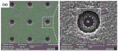
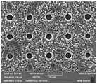
图1(a)是实施例1获得的高度有序图案化多孔微米金刚石薄膜扫描电镜照片,右侧图是左侧图中方框部位的放大图;Fig. 1 (a) is the scanning electron microscope photograph of the highly ordered patterned porous micron-diamond film obtained in Example 1, and the figure on the right is an enlarged view of the box part in the figure on the left;
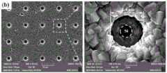
图1(b)是实施例2获得的高度有序图案化多孔微米金刚石薄膜扫描电镜照片,右侧图是左侧图中方框部位的放大图;Fig. 1 (b) is the scanning electron microscope photograph of the highly ordered patterned porous micron-diamond film obtained in Example 2, and the figure on the right is an enlarged view of the box part in the figure on the left;
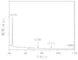
图2是实施例1获得的高度有序图案化多孔微米金刚石薄膜GIXRD表征结果;Fig. 2 is the highly ordered patterned porous micro-diamond film GIXRD characterization result obtained in Example 1;
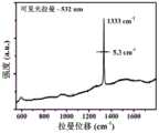
图3是实施例1获得的高度有序图案化多孔微米金刚石薄膜可见光Raman表征结果。3 is the visible light Raman characterization result of the highly ordered patterned porous micro-diamond film obtained in Example 1.
图4是实施例1获得的高度有序图案化多孔微米金刚石薄膜纳米压入力学性能表征结果。FIG. 4 is the characterization result of the nano-intrusion mechanical properties of the highly ordered patterned porous micro-diamond film obtained in Example 1.
图5是实施例5获得的金刚石薄膜的扫描电镜照片。5 is a scanning electron microscope photograph of the diamond thin film obtained in Example 5.
图6是对比例1获得的金刚石薄膜的扫描电镜照片。6 is a scanning electron microscope photograph of the diamond thin film obtained in Comparative Example 1.
图7是对比例2获得的金刚石薄膜的扫描电镜照片。7 is a scanning electron microscope photograph of the diamond thin film obtained in Comparative Example 2.
图8是对比例3获得的金刚石薄膜的扫描电镜照片。8 is a scanning electron microscope photograph of the diamond thin film obtained in Comparative Example 3.
图9是对比例4获得的金刚石薄膜的扫描电镜照片。9 is a scanning electron microscope photograph of the diamond thin film obtained in Comparative Example 4.
图10是对比例5获得的金刚石薄膜的扫描电镜照片。10 is a scanning electron microscope photograph of the diamond thin film obtained in Comparative Example 5.
图11是对比例6获得的金刚石薄膜的扫描电镜照片。11 is a scanning electron microscope photograph of the diamond thin film obtained in Comparative Example 6.
图12对比例7获得的金刚石薄膜的扫描电镜照片。FIG. 12 is a scanning electron microscope photograph of the diamond thin film obtained in Comparative Example 7.
具体实施方式Detailed ways
下面结合附图并通过具体实施方式来进一步说明本发明的技术方案。The technical solutions of the present invention are further described below with reference to the accompanying drawings and through specific embodiments.
实施例1Example 1
(1)采用Si(100)为基底,先后经过丙酮、酒精超声清洗,烘干后,采用纳米压印将周期性图案转移至硅基底表面得到图案化的硅基底,硅基上具有周期排布的圆柱形孔洞,孔洞直径为10μm,高度为4μm,相邻孔洞的距离为28μm,后再次经过丙酮、酒精超声清洗、烘干。(1) Using Si(100) as the substrate, after ultrasonic cleaning with acetone and alcohol successively, and drying, the periodic pattern is transferred to the surface of the silicon substrate by nano-imprinting to obtain a patterned silicon substrate. The silicon substrate has a periodic arrangement The diameter of the hole is 10 μm, the height is 4 μm, and the distance between adjacent holes is 28 μm, and then ultrasonically cleaned and dried with acetone and alcohol.
(2)取质量为25mg、晶粒尺寸为100nm的金刚石微粉,分散于50ml丙酮溶液中,将图案化的硅基底材料置于分散溶液中,超声清洗10min。随后取出预处理样品,并先后在丙酮、酒精超声清洗,然后烘干。(2) Take diamond micropowder with a mass of 25 mg and a grain size of 100 nm, disperse it in 50 ml of acetone solution, place the patterned silicon base material in the dispersion solution, and ultrasonically clean it for 10 min. Subsequently, the pretreated samples were taken out, and were ultrasonically cleaned in acetone and alcohol successively, and then dried.
(3)将预处理样品置于微波等离子体化学气相沉积反应室,本地真空抽至1.0×10⁻³Pa后开始沉积。(3) The pretreated sample was placed in a microwave plasma chemical vapor deposition reaction chamber, and the deposition was started after the local vacuum was pumped to 1.0×10⁻³ Pa.
(4)采用CH4、H2为工作气体,气体流量分别为14sccm和478sccm,工作气压150Torr,基底温度800℃,微波功率5000W,沉积时间15min,得到有序图案化多孔金刚石薄膜,薄膜在基底上表面的厚度3.5μm,薄膜孔底微孔直径4.3μm。(4) CH4 and H2 were used as working gases, the gas flow rates were 14 sccm and 478 sccm, the working pressure was 150 Torr, the substrate temperature was 800 °C, the microwave power was 5000 W, and the deposition time was 15 min to obtain an ordered patterned porous diamond film. The thickness of the upper surface is 3.5 μm, and the diameter of the pores at the bottom of the film hole is 4.3 μm.
图1(a)是实施例1获得的高度有序图案化多孔微米金刚石薄膜扫描电镜照片,右侧图是左侧图中方框部位的放大图,由图可以看出,所述多孔金刚石薄膜包括微米尺度的有序图案化的孔洞以及微米金刚石薄膜;所述孔洞的底面中空,所述微米金刚石薄膜连续且致密的分布在孔洞的底面边缘、侧壁以及非孔洞的位置,所述有序图案化的孔洞为圆柱型孔洞,孔洞按周期性排列,孔底微孔直径4.3μm。Figure 1(a) is a scanning electron microscope photograph of the highly ordered patterned porous micron-diamond film obtained in Example 1, and the figure on the right is an enlarged view of the box in the figure on the left. It can be seen from the figure that the porous diamond film includes Micron-scale ordered patterned holes and micro-diamond films; the bottom surface of the holes is hollow, and the micro-diamond films are continuously and densely distributed on the bottom edge, sidewalls and non-hole positions of the holes, the ordered pattern The formed holes are cylindrical holes, the holes are arranged periodically, and the diameter of the micropores at the bottom of the holes is 4.3 μm.
图2是实施例1获得的高度有序图案化多孔微米金刚石薄膜GIXRD表征结果,由图可以看出,所述微米金刚石薄膜为多晶结构,沿(111)晶面择优生长。2 is the GIXRD characterization result of the highly ordered patterned porous micro-diamond film obtained in Example 1. It can be seen from the figure that the micro-diamond film has a polycrystalline structure and grows preferentially along the (111) crystal plane.
图3是实施例1获得的高度有序图案化多孔微米金刚石薄膜可见光Raman表征结果,由图可以看出,所述微米金刚石薄膜拉曼特征峰位于1333cm-1,半峰宽5.3cm-1。3 is the visible light Raman characterization result of the highly ordered patterned porous micro-diamond film obtained in Example 1. It can be seen from the figure that the Raman characteristic peak of the micro-diamond film is located at 1333 cm-1 and the half-peak width is 5.3 cm-1 .
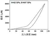
图4是实施例1获得的高度有序图案化多孔微米金刚石薄膜纳米压入力学性能表征结果,由图可以看出,所获得微米金刚石薄膜的显微硬度可达62GPa,弹性模量647GPa。Figure 4 shows the results of nano-intrusion mechanical properties of the highly ordered patterned porous micro-diamond film obtained in Example 1. It can be seen from the figure that the micro-hardness of the obtained micro-diamond film can reach 62GPa and the elastic modulus is 647GPa.
实施例2Example 2
(1)采用Si(100)为基底,先后经过丙酮、酒精超声清洗,烘干后,采用纳米压印将周期性图案转移至硅基底表面,图案为周期排布的圆柱形孔洞,孔洞的直径为10μm,深度为4μm,相邻孔洞的距离为28μm,后再次经过丙酮、酒精超声清洗、烘干。(1) Using Si (100) as the substrate, after ultrasonic cleaning with acetone and alcohol successively, after drying, the periodic pattern is transferred to the surface of the silicon substrate by nano-imprinting. The pattern is a periodically arranged cylindrical hole, and the diameter of the hole is It is 10 μm, the depth is 4 μm, and the distance between adjacent holes is 28 μm, and then ultrasonically cleaned and dried with acetone and alcohol again.
(2)取质量为25mg、晶粒尺寸为100nm的金刚石微粉,分散于50ml丙酮溶液中,将图案化的硅基底材料置于分散溶液中,超声清洗10min。随后取出预处理样品,并先后在丙酮、酒精超声清洗,然后烘干。(2) Take diamond micropowder with a mass of 25 mg and a grain size of 100 nm, disperse it in 50 ml of acetone solution, place the patterned silicon base material in the dispersion solution, and ultrasonically clean it for 10 min. Subsequently, the pretreated samples were taken out, and were ultrasonically cleaned in acetone and alcohol successively, and then dried.
(3)将预处理样品置于微波等离子体化学气相沉积反应室,本地真空抽至1.0×10⁻³Pa后开始沉积。(3) The pretreated sample was placed in a microwave plasma chemical vapor deposition reaction chamber, and the deposition was started after the local vacuum was pumped to 1.0×10⁻³ Pa.
(4)采用CH4、H2为工作气体,气体流量分别为14和478sccm,工作气压150Torr,基底温度850℃,微波射频功率5000W,沉积时间20min。(4) CH4 and H2 were used as working gases, the gas flow rates were 14 and 478 sccm respectively, the working pressure was 150 Torr, the substrate temperature was 850° C., the microwave radio frequency power was 5000 W, and the deposition time was 20 min.
图1(b)是实施例2获得的高度有序图案化多孔微米金刚石薄膜扫描电镜照片,右侧图是左侧图中方框部位的放大图,由图可以看出,所述多孔金刚石薄膜包括微米尺度的有序图案化的孔洞以及微米金刚石薄膜;所述孔洞的底面中空,所述微米金刚石薄膜连续且致密的分布在孔洞的底面边缘、侧壁以及非孔洞的位置,所述有序图案化的孔洞为圆柱型孔洞,孔洞按周期性排列,薄膜在基底上表面的厚度4.7μm,薄膜孔底微孔直径1.8μm。Fig. 1(b) is a scanning electron microscope photograph of the highly ordered patterned porous micron-diamond film obtained in Example 2. The figure on the right is an enlarged view of the box portion in the figure on the left. It can be seen from the figure that the porous diamond film includes Micron-scale ordered patterned holes and micro-diamond films; the bottom surface of the holes is hollow, and the micro-diamond films are continuously and densely distributed on the bottom edge, sidewalls and non-hole positions of the holes, the ordered pattern The formed holes are cylindrical holes, the holes are arranged periodically, the thickness of the film on the upper surface of the substrate is 4.7 μm, and the diameter of the micropores at the bottom of the film hole is 1.8 μm.
实施例3Example 3
(1)采用Si(100)为基底,先后经过丙酮、酒精超声清洗,烘干后,采用纳米压印将周期性图案转移至硅基底表面,图案为周期排布的圆柱形孔洞,孔洞的直径为10μm,深度为4μm,相邻孔洞的距离为28μm,后再次经过丙酮、酒精超声清洗、烘干。(1) Using Si (100) as the substrate, after ultrasonic cleaning with acetone and alcohol successively, after drying, the periodic pattern is transferred to the surface of the silicon substrate by nano-imprinting. The pattern is a periodically arranged cylindrical hole, and the diameter of the hole is It is 10 μm, the depth is 4 μm, and the distance between adjacent holes is 28 μm, and then ultrasonically cleaned and dried with acetone and alcohol again.
(2)取质量为20mg、晶粒尺寸为150nm的金刚石微粉,分散于40ml丙酮溶液中,将图案化的硅基底材料置于分散溶液中,超声清洗8min。随后取出预处理样品,并先后在丙酮、酒精超声清洗,然后烘干。(2) Take diamond micropowder with a mass of 20 mg and a grain size of 150 nm, disperse it in 40 ml of acetone solution, place the patterned silicon base material in the dispersion solution, and ultrasonically clean it for 8 minutes. Subsequently, the pretreated samples were taken out, and were ultrasonically cleaned in acetone and alcohol successively, and then dried.
(3)将预处理样品置于微波等离子体化学气相沉积反应室,本地真空抽至1.0×10⁻³Pa后开始沉积。(3) The pretreated sample was placed in a microwave plasma chemical vapor deposition reaction chamber, and the deposition was started after the local vacuum was pumped to 1.0×10⁻³ Pa.
(4)采用CH4、H2为工作气体,气体流量分别为25sccm和478sccm,工作气压160Torr,基底温度900℃,微波射频功率4000W,沉积时间35min。(4) CH4 and H2 were used as the working gases, the gas flow rates were 25 sccm and 478 sccm, the working pressure was 160 Torr, the substrate temperature was 900 °C, the microwave radio frequency power was 4000 W, and the deposition time was 35 min.
本实施例获得的多孔金刚石薄膜包括微米尺度的有序图案化的孔洞以及微米金刚石薄膜;所述孔洞的底面中空,所述微米金刚石薄膜连续且致密的分布在孔洞的底面边缘、侧壁以及非孔洞的位置,所述有序图案化的孔洞为圆柱型孔洞,孔洞按周期性排列。The porous diamond film obtained in this example includes micron-scale ordered patterned holes and a micron-diamond film; the bottom surface of the hole is hollow, and the micro-diamond film is continuously and densely distributed on the bottom edge, sidewall and non-contact surface of the hole. The positions of the holes, the orderly patterned holes are cylindrical holes, and the holes are arranged periodically.
实施例4Example 4
(1)采用Si(100)为基底,先后经过丙酮、酒精超声清洗,烘干后,采用纳米压印将周期性图案转移至硅基底表面,图案为周期排布的圆柱形孔洞,孔洞的直径为10μm,深度为4μm,相邻孔洞的距离为28μm,后再次经过丙酮、酒精超声清洗、烘干。(1) Using Si (100) as the substrate, after ultrasonic cleaning with acetone and alcohol successively, after drying, the periodic pattern is transferred to the surface of the silicon substrate by nano-imprinting. The pattern is a periodically arranged cylindrical hole, and the diameter of the hole is It is 10 μm, the depth is 4 μm, and the distance between adjacent holes is 28 μm, and then ultrasonically cleaned and dried with acetone and alcohol again.
(2)取质量为50mg、晶粒尺寸为300nm的金刚石微粉,分散于100ml乙醇溶液中,将图案化的硅基底材料置于分散溶液中,超声清洗10min。随后取出预处理样品,并先后在丙酮、酒精超声清洗,然后烘干。(2) Take diamond micropowder with a mass of 50 mg and a grain size of 300 nm, disperse it in 100 ml of ethanol solution, place the patterned silicon base material in the dispersion solution, and ultrasonically clean it for 10 min. Subsequently, the pretreated samples were taken out, and were ultrasonically cleaned in acetone and alcohol successively, and then dried.
(3)将预处理样品置于微波等离子体化学气相沉积反应室,本地真空抽至1.0×10⁻³Pa后开始沉积。(3) The pretreated sample was placed in a microwave plasma chemical vapor deposition reaction chamber, and the deposition was started after the local vacuum was pumped to 1.0×10⁻³ Pa.
(4)采用CH4、H2为工作气体,气体流量分别为40sccm和478sccm,工作气压115Torr,基底温度875℃,微波射频功率4500W,沉积时间30min。(4) CH4 and H2 were used as working gases, the gas flow rates were 40 sccm and 478 sccm, the working pressure was 115 Torr, the substrate temperature was 875° C., the microwave radio frequency power was 4500 W, and the deposition time was 30 min.
本实施例获得的多孔金刚石薄膜包括微米尺度的有序图案化的孔洞以及微米金刚石薄膜;所述孔洞的底面中空,所述微米金刚石薄膜连续且致密的分布在孔洞的底面边缘、侧壁以及非孔洞的位置,所述有序图案化的孔洞为圆柱型孔洞,孔洞按周期性排列。The porous diamond film obtained in this example includes micron-scale ordered patterned holes and a micron-diamond film; the bottom surface of the hole is hollow, and the micro-diamond film is continuously and densely distributed on the bottom edge, sidewall and non-contact surface of the hole. The positions of the holes, the orderly patterned holes are cylindrical holes, and the holes are arranged periodically.
实施例5Example 5
与实施例1的区别在于,沉积时间为30min,薄膜厚度5.1μm,薄膜孔底微孔直径1.2μm,薄膜表面连续且致密,孔壁处薄膜覆盖连续。The difference from Example 1 is that the deposition time is 30 min, the film thickness is 5.1 μm, the diameter of the pores at the bottom of the film is 1.2 μm, the surface of the film is continuous and dense, and the film covering the hole wall is continuous.
对比例1Comparative Example 1
除了未进行步骤(2)预处理步骤,而直接将步骤(1)所得硅片用于步骤(3)外,其他制备方法和条件与实施例1相同。Except that the pretreatment step of step (2) is not performed, and the silicon wafer obtained in step (1) is directly used in step (3), other preparation methods and conditions are the same as those of
本对比例未进行预处理步骤,导致薄膜生长初期形核率低,薄膜生长速率慢,表面不连续,孔洞侧壁难以沉积成膜。In this comparative example, no pretreatment step was performed, resulting in a low nucleation rate at the initial stage of film growth, slow film growth rate, discontinuous surface, and difficulty in deposition and film formation on the side walls of the holes.
对比例2Comparative Example 2
除了将步骤(4)沉积时间调整为5min外,其他制备方法和条件与实施例1相同。Except that the deposition time in step (4) was adjusted to 5 min, other preparation methods and conditions were the same as those in Example 1.
本对比例沉积时间过短,形核密度较对比例明显提高,但薄膜表面仍不连续。The deposition time of this comparative example is too short, and the nucleation density is obviously higher than that of the comparative example, but the film surface is still discontinuous.
对比例3Comparative Example 3
(1)采用Si(100)为基底,先后经过丙酮、酒精超声清洗,烘干后,采用纳米压印将周期性图案转移至硅基底表面,图案为周期排布的圆柱形孔洞,孔洞的直径为10μm,深度为4μm,相邻孔洞的距离为28μm,后再次经过丙酮、酒精超声清洗、烘干。(1) Using Si (100) as the substrate, after ultrasonic cleaning with acetone and alcohol successively, after drying, the periodic pattern is transferred to the surface of the silicon substrate by nano-imprinting. The pattern is a periodically arranged cylindrical hole, and the diameter of the hole is It is 10 μm, the depth is 4 μm, and the distance between adjacent holes is 28 μm, and then ultrasonically cleaned and dried with acetone and alcohol again.
(2)取质量为30mg、晶粒尺寸为200nm的金刚石微粉,分散于50ml乙醇溶液中,将图案化的硅基底材料置于分散溶液中,超声清洗8min。随后取出预处理样品,并先后在丙酮、酒精超声清洗,然后烘干。(2) Take diamond micropowder with a mass of 30 mg and a grain size of 200 nm, disperse it in 50 ml of ethanol solution, place the patterned silicon base material in the dispersion solution, and ultrasonically clean it for 8 minutes. Subsequently, the pretreated samples were taken out, and were ultrasonically cleaned in acetone and alcohol successively, and then dried.
(3)将预处理样品置于微波等离子体化学气相沉积反应室,本地真空抽至1.5×10⁻³Pa后开始沉积。(3) The pretreated sample was placed in a microwave plasma chemical vapor deposition reaction chamber, and the deposition was started after the local vacuum was pumped to 1.5×10⁻³ Pa.
(4)采用CH4、H2为工作气体,气体流量分别为25sccm和478sccm,工作气压125Torr,基底温度750℃,微波射频功率4000W,沉积时间10min。(4) CH4 and H2 were used as the working gases, the gas flow rates were 25 sccm and 478 sccm, the working pressure was 125 Torr, the substrate temperature was 750° C., the microwave radio frequency power was 4000 W, and the deposition time was 10 min.
本对比例的沉积时间较短,虽然气体流量、基底温度和微波射频功率等在合理的范围内,依然无法得到连续致密的微米金刚石薄膜。The deposition time of this comparative example is short, and although the gas flow rate, substrate temperature and microwave radio frequency power are within a reasonable range, it is still impossible to obtain a continuous and dense micron-diamond film.
对比例4Comparative Example 4
与对比例3的区别在于,CH4的气体流量分别为30sccm。The difference from Comparative Example 3 is that the gas flow rates ofCH4 are 30 sccm, respectively.
与对比例3相比,虽然提高了工作气体中CH4含量,薄膜生长速率及形核密度增加,微米金刚石平均粒径尺寸变小,依然无法获得致密连续的微米金刚石薄膜。Compared with Comparative Example 3, although the CH4 content in the working gas is increased, the film growth rate and nucleation density are increased, and the average particle size of the micro-diamond is reduced, but a dense and continuous micro-diamond film cannot be obtained.
对比例5Comparative Example 5
与实施例1的区别在于,沉积功率为2500W,沉积时间为5min,薄膜在孔洞附近不连续,微孔侧壁薄膜沉积不充分不完整。The difference from Example 1 is that the deposition power is 2500W, the deposition time is 5min, the film is discontinuous near the hole, and the film deposition on the sidewall of the micropore is insufficient and incomplete.
由此可知,在沉积时间过短的情况下,即使沉积功率在预选范围内也难以获得致密连续的微米金刚石薄膜。It can be seen that when the deposition time is too short, it is difficult to obtain a dense and continuous micro-diamond film even if the deposition power is within the preselected range.
对比例6Comparative Example 6
与实施例1的区别在于,沉积温度为650℃,生长速度慢,薄膜在孔洞附近不连续,微孔侧壁薄膜沉积不充分不完整。The difference from Example 1 is that the deposition temperature is 650° C., the growth rate is slow, the film is discontinuous near the hole, and the film deposition on the sidewall of the micropore is insufficient and incomplete.
对比例7Comparative Example 7
与实施例1的区别在于,沉积温度为950℃,沉积时间为5min,薄膜在孔洞附近不连续,微孔侧壁薄膜沉积不充分不完整。The difference from Example 1 is that the deposition temperature is 950° C., the deposition time is 5 minutes, the film is discontinuous near the hole, and the film deposition on the sidewall of the micropore is insufficient and incomplete.
由此可知,在沉积时间过短的情况下,即使提高沉积温度也难以获得致密连续的微米金刚石薄膜。It can be seen that when the deposition time is too short, it is difficult to obtain a dense and continuous micro-diamond film even if the deposition temperature is increased.
申请人声明,本发明通过上述实施例来说明本发明的详细方法,但本发明并不局限于上述详细方法,即不意味着本发明必须依赖上述详细方法才能实施。所属技术领域的技术人员应该明了,对本发明的任何改进,对本发明产品各原料的等效替换及辅助成分的添加、具体方式的选择等,均落在本发明的保护范围和公开范围之内。The applicant declares that the present invention illustrates the detailed method of the present invention through the above-mentioned embodiments, but the present invention is not limited to the above-mentioned detailed method, that is, it does not mean that the present invention must rely on the above-mentioned detailed method to be implemented. Those skilled in the art should understand that any improvement of the present invention, the equivalent replacement of each raw material of the product of the present invention, the addition of auxiliary components, the selection of specific methods, etc., all fall within the protection scope and disclosure scope of the present invention.
Claims (10)
Translated fromChinesePriority Applications (1)
| Application Number | Priority Date | Filing Date | Title |
|---|---|---|---|
| CN202010611752.7ACN112011784B (en) | 2020-06-29 | 2020-06-29 | An ordered patterned porous diamond film and its preparation method and use |
Applications Claiming Priority (1)
| Application Number | Priority Date | Filing Date | Title |
|---|---|---|---|
| CN202010611752.7ACN112011784B (en) | 2020-06-29 | 2020-06-29 | An ordered patterned porous diamond film and its preparation method and use |
Publications (2)
| Publication Number | Publication Date |
|---|---|
| CN112011784Atrue CN112011784A (en) | 2020-12-01 |
| CN112011784B CN112011784B (en) | 2022-09-20 |
Family
ID=73498428
Family Applications (1)
| Application Number | Title | Priority Date | Filing Date |
|---|---|---|---|
| CN202010611752.7AActiveCN112011784B (en) | 2020-06-29 | 2020-06-29 | An ordered patterned porous diamond film and its preparation method and use |
Country Status (1)
| Country | Link |
|---|---|
| CN (1) | CN112011784B (en) |
Cited By (5)
| Publication number | Priority date | Publication date | Assignee | Title |
|---|---|---|---|---|
| CN113088921A (en)* | 2021-04-13 | 2021-07-09 | 昆明理工大学 | Preparation method of porous diamond film/three-dimensional carbon nanowire network composite material and product thereof |
| CN113388822A (en)* | 2021-06-10 | 2021-09-14 | 南方科技大学 | Diamond film with topological pattern on surface and preparation method and application thereof |
| CN114717655A (en)* | 2022-04-21 | 2022-07-08 | 哈尔滨工业大学 | Crystal internal patterning method for diamond customized patterns and electrodes |
| CN115369386A (en)* | 2022-08-15 | 2022-11-22 | 北京科技大学 | A method of depositing diamond on a microstructured substrate |
| JP2024520600A (en)* | 2021-06-03 | 2024-05-24 | エコール ポリテクニーク フェデラル ド ローザンヌ (ウペエフエル) | Diamond device or structure and method for manufacturing diamond device or structure |
Citations (4)
| Publication number | Priority date | Publication date | Assignee | Title |
|---|---|---|---|---|
| US20070158872A1 (en)* | 2005-10-18 | 2007-07-12 | Korea Institute Of Machinery & Materials | Stamp for micro/nano imprint lithography using diamond-like carbon and method of fabricating the same |
| CN102127751A (en)* | 2011-01-11 | 2011-07-20 | 大连理工大学 | Boron-doped diamond micro-nano material with columnar array structure and preparation method thereof |
| US20190314766A1 (en)* | 2018-04-16 | 2019-10-17 | Imec Vzw | Formation of Diamond Membranes |
| CN110557936A (en)* | 2019-10-11 | 2019-12-10 | 陕西科技大学 | A kind of diamond microchannel Cu-based CVD diamond heat sink and its preparation method |
- 2020
- 2020-06-29CNCN202010611752.7Apatent/CN112011784B/enactiveActive
Patent Citations (4)
| Publication number | Priority date | Publication date | Assignee | Title |
|---|---|---|---|---|
| US20070158872A1 (en)* | 2005-10-18 | 2007-07-12 | Korea Institute Of Machinery & Materials | Stamp for micro/nano imprint lithography using diamond-like carbon and method of fabricating the same |
| CN102127751A (en)* | 2011-01-11 | 2011-07-20 | 大连理工大学 | Boron-doped diamond micro-nano material with columnar array structure and preparation method thereof |
| US20190314766A1 (en)* | 2018-04-16 | 2019-10-17 | Imec Vzw | Formation of Diamond Membranes |
| CN110557936A (en)* | 2019-10-11 | 2019-12-10 | 陕西科技大学 | A kind of diamond microchannel Cu-based CVD diamond heat sink and its preparation method |
Non-Patent Citations (1)
| Title |
|---|
| 钱苗根: "《现代表面工程》", 30 September 2012, 上海交通大学出版社* |
Cited By (5)
| Publication number | Priority date | Publication date | Assignee | Title |
|---|---|---|---|---|
| CN113088921A (en)* | 2021-04-13 | 2021-07-09 | 昆明理工大学 | Preparation method of porous diamond film/three-dimensional carbon nanowire network composite material and product thereof |
| JP2024520600A (en)* | 2021-06-03 | 2024-05-24 | エコール ポリテクニーク フェデラル ド ローザンヌ (ウペエフエル) | Diamond device or structure and method for manufacturing diamond device or structure |
| CN113388822A (en)* | 2021-06-10 | 2021-09-14 | 南方科技大学 | Diamond film with topological pattern on surface and preparation method and application thereof |
| CN114717655A (en)* | 2022-04-21 | 2022-07-08 | 哈尔滨工业大学 | Crystal internal patterning method for diamond customized patterns and electrodes |
| CN115369386A (en)* | 2022-08-15 | 2022-11-22 | 北京科技大学 | A method of depositing diamond on a microstructured substrate |
Also Published As
| Publication number | Publication date |
|---|---|
| CN112011784B (en) | 2022-09-20 |
Similar Documents
| Publication | Publication Date | Title |
|---|---|---|
| CN112011784B (en) | An ordered patterned porous diamond film and its preparation method and use | |
| US8597738B2 (en) | Fabrication of single-crystalline graphene arrays | |
| JP3995698B2 (en) | Method for forming catalyst layer for synthesis of carbon nanotube and method for producing carbon nanotube using the same | |
| JP4665720B2 (en) | Pattern substrate, pattern substrate manufacturing method, fine mold, and magnetic recording pattern medium | |
| JP5405574B2 (en) | Templates and methods for producing high aspect ratio templates for lithography, and use of templates to drill substrates at the nanoscale | |
| US20160368773A1 (en) | Nanostructured graphene with atomically-smooth edges | |
| US6350389B1 (en) | Method for producing porous diamond | |
| KR102232418B1 (en) | Graphene membrane and method for manufacturing the same | |
| JP2012142065A (en) | System and method for imprint-guided block copolymer patterning | |
| JP2009155111A5 (en) | ||
| CN102556952A (en) | Metal cup-cylinder composite nano structure array and preparation method thereof | |
| CN102431962A (en) | Preparation method and application of nanoimprint template | |
| CN114959633B (en) | Diamond micro-nano composite structure tool for processing hydrophobic surface of workpiece and preparation method thereof | |
| KR101383758B1 (en) | Method of forming porous carbon structure and porous carbon structure prepared by the same | |
| CN108622848A (en) | A kind of three-dimensional composite nanostructure of large area and preparation method thereof | |
| CN109666917B (en) | Diamond surface structure and preparation method thereof | |
| CN105621353B (en) | A kind of large-area nano graphic method based on multi-layered anode alumina formwork | |
| CN107180897B (en) | A kind of preparation method of nanometer optoelectronic device based on nanosieve mask | |
| Ono et al. | Pattern transfer of self-ordered structure with diamond mold | |
| CN103803618B (en) | A kind of preparation method of porous anodic aluminium oxide 3-D nano, structure | |
| CN105568228A (en) | Preparation method of radial metal nanowire-ceramic composite film | |
| CN110244514B (en) | Photoresist with nanopore structure on surface and preparation method thereof | |
| KR20240165286A (en) | Scalable fabrication of large-scale, ultraflat and transferable polycrystalline diamond membranes | |
| JP5208108B2 (en) | Photonic crystal manufacturing method | |
| Asoh et al. | Pt–Pd-embedded silicon microwell arrays |
Legal Events
| Date | Code | Title | Description |
|---|---|---|---|
| PB01 | Publication | ||
| PB01 | Publication | ||
| SE01 | Entry into force of request for substantive examination | ||
| SE01 | Entry into force of request for substantive examination | ||
| GR01 | Patent grant | ||
| GR01 | Patent grant |