CN112005350A - semiconductor device - Google Patents
semiconductor deviceDownload PDFInfo
- Publication number
- CN112005350A CN112005350ACN201980027125.4ACN201980027125ACN112005350ACN 112005350 ACN112005350 ACN 112005350ACN 201980027125 ACN201980027125 ACN 201980027125ACN 112005350 ACN112005350 ACN 112005350A
- Authority
- CN
- China
- Prior art keywords
- oxide
- insulator
- conductor
- transistor
- addition
- Prior art date
- Legal status (The legal status is an assumption and is not a legal conclusion. Google has not performed a legal analysis and makes no representation as to the accuracy of the status listed.)
- Pending
Links
Images


Classifications
- H—ELECTRICITY
- H10—SEMICONDUCTOR DEVICES; ELECTRIC SOLID-STATE DEVICES NOT OTHERWISE PROVIDED FOR
- H10D—INORGANIC ELECTRIC SEMICONDUCTOR DEVICES
- H10D30/00—Field-effect transistors [FET]
- H10D30/60—Insulated-gate field-effect transistors [IGFET]
- H10D30/67—Thin-film transistors [TFT]
- H10D30/674—Thin-film transistors [TFT] characterised by the active materials
- H10D30/6755—Oxide semiconductors, e.g. zinc oxide, copper aluminium oxide or cadmium stannate
- H—ELECTRICITY
- H10—SEMICONDUCTOR DEVICES; ELECTRIC SOLID-STATE DEVICES NOT OTHERWISE PROVIDED FOR
- H10D—INORGANIC ELECTRIC SEMICONDUCTOR DEVICES
- H10D62/00—Semiconductor bodies, or regions thereof, of devices having potential barriers
- H10D62/80—Semiconductor bodies, or regions thereof, of devices having potential barriers characterised by the materials
- H—ELECTRICITY
- H01—ELECTRIC ELEMENTS
- H01L—SEMICONDUCTOR DEVICES NOT COVERED BY CLASS H10
- H01L21/00—Processes or apparatus adapted for the manufacture or treatment of semiconductor or solid state devices or of parts thereof
- H01L21/70—Manufacture or treatment of devices consisting of a plurality of solid state components formed in or on a common substrate or of parts thereof; Manufacture of integrated circuit devices or of parts thereof
- H01L21/71—Manufacture of specific parts of devices defined in group H01L21/70
- H01L21/768—Applying interconnections to be used for carrying current between separate components within a device comprising conductors and dielectrics
- H—ELECTRICITY
- H01—ELECTRIC ELEMENTS
- H01L—SEMICONDUCTOR DEVICES NOT COVERED BY CLASS H10
- H01L23/00—Details of semiconductor or other solid state devices
- H01L23/52—Arrangements for conducting electric current within the device in operation from one component to another, i.e. interconnections, e.g. wires, lead frames
- H01L23/522—Arrangements for conducting electric current within the device in operation from one component to another, i.e. interconnections, e.g. wires, lead frames including external interconnections consisting of a multilayer structure of conductive and insulating layers inseparably formed on the semiconductor body
- H01L23/532—Arrangements for conducting electric current within the device in operation from one component to another, i.e. interconnections, e.g. wires, lead frames including external interconnections consisting of a multilayer structure of conductive and insulating layers inseparably formed on the semiconductor body characterised by the materials
- H—ELECTRICITY
- H10—SEMICONDUCTOR DEVICES; ELECTRIC SOLID-STATE DEVICES NOT OTHERWISE PROVIDED FOR
- H10B—ELECTRONIC MEMORY DEVICES
- H10B12/00—Dynamic random access memory [DRAM] devices
- H10B12/30—DRAM devices comprising one-transistor - one-capacitor [1T-1C] memory cells
- H—ELECTRICITY
- H10—SEMICONDUCTOR DEVICES; ELECTRIC SOLID-STATE DEVICES NOT OTHERWISE PROVIDED FOR
- H10B—ELECTRONIC MEMORY DEVICES
- H10B12/00—Dynamic random access memory [DRAM] devices
- H10B12/30—DRAM devices comprising one-transistor - one-capacitor [1T-1C] memory cells
- H10B12/31—DRAM devices comprising one-transistor - one-capacitor [1T-1C] memory cells having a storage electrode stacked over the transistor
- H10B12/312—DRAM devices comprising one-transistor - one-capacitor [1T-1C] memory cells having a storage electrode stacked over the transistor with a bit line higher than the capacitor
- H—ELECTRICITY
- H10—SEMICONDUCTOR DEVICES; ELECTRIC SOLID-STATE DEVICES NOT OTHERWISE PROVIDED FOR
- H10D—INORGANIC ELECTRIC SEMICONDUCTOR DEVICES
- H10D30/00—Field-effect transistors [FET]
- H10D30/60—Insulated-gate field-effect transistors [IGFET]
- H10D30/67—Thin-film transistors [TFT]
- H10D30/6729—Thin-film transistors [TFT] characterised by the electrodes
- H10D30/673—Thin-film transistors [TFT] characterised by the electrodes characterised by the shapes, relative sizes or dispositions of the gate electrodes
- H10D30/6733—Multi-gate TFTs
- H10D30/6734—Multi-gate TFTs having gate electrodes arranged on both top and bottom sides of the channel, e.g. dual-gate TFTs
- H—ELECTRICITY
- H10—SEMICONDUCTOR DEVICES; ELECTRIC SOLID-STATE DEVICES NOT OTHERWISE PROVIDED FOR
- H10D—INORGANIC ELECTRIC SEMICONDUCTOR DEVICES
- H10D86/00—Integrated devices formed in or on insulating or conducting substrates, e.g. formed in silicon-on-insulator [SOI] substrates or on stainless steel or glass substrates
- H10D86/40—Integrated devices formed in or on insulating or conducting substrates, e.g. formed in silicon-on-insulator [SOI] substrates or on stainless steel or glass substrates characterised by multiple TFTs
- H10D86/421—Integrated devices formed in or on insulating or conducting substrates, e.g. formed in silicon-on-insulator [SOI] substrates or on stainless steel or glass substrates characterised by multiple TFTs having a particular composition, shape or crystalline structure of the active layer
- H10D86/423—Integrated devices formed in or on insulating or conducting substrates, e.g. formed in silicon-on-insulator [SOI] substrates or on stainless steel or glass substrates characterised by multiple TFTs having a particular composition, shape or crystalline structure of the active layer comprising semiconductor materials not belonging to the Group IV, e.g. InGaZnO
- H—ELECTRICITY
- H10—SEMICONDUCTOR DEVICES; ELECTRIC SOLID-STATE DEVICES NOT OTHERWISE PROVIDED FOR
- H10D—INORGANIC ELECTRIC SEMICONDUCTOR DEVICES
- H10D86/00—Integrated devices formed in or on insulating or conducting substrates, e.g. formed in silicon-on-insulator [SOI] substrates or on stainless steel or glass substrates
- H10D86/40—Integrated devices formed in or on insulating or conducting substrates, e.g. formed in silicon-on-insulator [SOI] substrates or on stainless steel or glass substrates characterised by multiple TFTs
- H10D86/60—Integrated devices formed in or on insulating or conducting substrates, e.g. formed in silicon-on-insulator [SOI] substrates or on stainless steel or glass substrates characterised by multiple TFTs wherein the TFTs are in active matrices
- H—ELECTRICITY
- H10—SEMICONDUCTOR DEVICES; ELECTRIC SOLID-STATE DEVICES NOT OTHERWISE PROVIDED FOR
- H10B—ELECTRONIC MEMORY DEVICES
- H10B41/00—Electrically erasable-and-programmable ROM [EEPROM] devices comprising floating gates
- H10B41/70—Electrically erasable-and-programmable ROM [EEPROM] devices comprising floating gates the floating gate being an electrode shared by two or more components
- H—ELECTRICITY
- H10—SEMICONDUCTOR DEVICES; ELECTRIC SOLID-STATE DEVICES NOT OTHERWISE PROVIDED FOR
- H10D—INORGANIC ELECTRIC SEMICONDUCTOR DEVICES
- H10D84/00—Integrated devices formed in or on semiconductor substrates that comprise only semiconducting layers, e.g. on Si wafers or on GaAs-on-Si wafers
- H10D84/01—Manufacture or treatment
- H10D84/02—Manufacture or treatment characterised by using material-based technologies
- H10D84/08—Manufacture or treatment characterised by using material-based technologies using combinations of technologies, e.g. using both Si and SiC technologies or using both Si and Group III-V technologies
- H—ELECTRICITY
- H10—SEMICONDUCTOR DEVICES; ELECTRIC SOLID-STATE DEVICES NOT OTHERWISE PROVIDED FOR
- H10D—INORGANIC ELECTRIC SEMICONDUCTOR DEVICES
- H10D84/00—Integrated devices formed in or on semiconductor substrates that comprise only semiconducting layers, e.g. on Si wafers or on GaAs-on-Si wafers
- H10D84/80—Integrated devices formed in or on semiconductor substrates that comprise only semiconducting layers, e.g. on Si wafers or on GaAs-on-Si wafers characterised by the integration of at least one component covered by groups H10D12/00 or H10D30/00, e.g. integration of IGFETs
- H10D84/811—Combinations of field-effect devices and one or more diodes, capacitors or resistors
- H—ELECTRICITY
- H10—SEMICONDUCTOR DEVICES; ELECTRIC SOLID-STATE DEVICES NOT OTHERWISE PROVIDED FOR
- H10D—INORGANIC ELECTRIC SEMICONDUCTOR DEVICES
- H10D88/00—Three-dimensional [3D] integrated devices
Landscapes
- Engineering & Computer Science (AREA)
- Microelectronics & Electronic Packaging (AREA)
- Condensed Matter Physics & Semiconductors (AREA)
- General Physics & Mathematics (AREA)
- Computer Hardware Design (AREA)
- Physics & Mathematics (AREA)
- Power Engineering (AREA)
- Manufacturing & Machinery (AREA)
- Thin Film Transistor (AREA)
- Semiconductor Memories (AREA)
- Metal-Oxide And Bipolar Metal-Oxide Semiconductor Integrated Circuits (AREA)
- Internal Circuitry In Semiconductor Integrated Circuit Devices (AREA)
- Semiconductor Integrated Circuits (AREA)
- Non-Volatile Memory (AREA)
Abstract
Description
Translated fromChinese技术领域technical field
本发明的一个方式涉及一种半导体装置及半导体装置的制造方法。此外,本发明的一个方式涉及一种半导体晶片、模块以及电子设备。One embodiment of the present invention relates to a semiconductor device and a method of manufacturing the semiconductor device. Furthermore, one aspect of the present invention relates to a semiconductor wafer, a module, and an electronic device.
注意,在本说明书等中,半导体装置是指能够通过利用半导体特性而工作的所有装置。除了晶体管等的半导体元件之外,半导体电路、运算装置或存储装置也是半导体装置的一个方式。显示装置(液晶显示装置、发光显示装置等)、投影装置、照明装置、电光装置、蓄电装置、存储装置、半导体电路、摄像装置及电子设备等有时包括半导体装置。Note that, in this specification and the like, a semiconductor device refers to all devices that can operate by utilizing semiconductor characteristics. In addition to semiconductor elements such as transistors, a semiconductor circuit, an arithmetic device, or a storage device is also one form of a semiconductor device. Display devices (liquid crystal display devices, light-emitting display devices, etc.), projection devices, lighting devices, electro-optical devices, power storage devices, storage devices, semiconductor circuits, imaging devices, electronic equipment, and the like may include semiconductor devices.
注意,本发明的一个方式不局限于上述技术领域。本说明书等所公开的发明的一个方式涉及一种物体、方法或制造方法。另外,本发明的一个方式涉及一种工序(process)、机器(machine)、产品(manufacture)或者组合物(composition of matter)。Note that one form of the present invention is not limited to the above-mentioned technical field. One aspect of the invention disclosed in this specification and the like relates to an object, a method, or a manufacturing method. Moreover, one form of this invention relates to a process (process), machine (machine), product (manufacture) or composition (composition of matter).
背景技术Background technique
作为可以应用于晶体管的半导体薄膜,硅类半导体材料被广泛地周知。另外,作为其他材料,氧化物半导体受到关注。作为氧化物半导体,例如,已知除了如氧化铟、氧化锌等单元金属氧化物之外还有多元金属氧化物。在多元金属氧化物中,有关In-Ga-Zn氧化物(以下也称为IGZO)的研究尤为火热。Silicon-based semiconductor materials are widely known as semiconductor thin films that can be applied to transistors. In addition, as other materials, oxide semiconductors are attracting attention. As the oxide semiconductor, for example, multi-component metal oxides are known in addition to unitary metal oxides such as indium oxide and zinc oxide. Among the multi-component metal oxides, the research on In-Ga-Zn oxide (hereinafter also referred to as IGZO) is particularly hot.
通过对IGZO的研究,在氧化物半导体中,发现了既不是单晶也不是非晶的CAAC(c-axis aligned crystalline:c轴取向结晶)结构及nc(nanocrystalline:纳米晶)结构(参照非专利文献1至非专利文献3)。非专利文献1及非专利文献2中公开了一种使用具有CAAC结构的氧化物半导体制造晶体管的技术。再者,非专利文献4及非专利文献5中公开了一种比CAAC结构及nc结构的结晶性更低的氧化物半导体中也具有微小的结晶。Through research on IGZO, in oxide semiconductors, CAAC (c-axis aligned crystalline: c-axis aligned crystalline) structure and nc (nanocrystalline: nanocrystalline) structure that are neither single crystal nor amorphous have been found (refer to non-patent).
将IGZO用于活性层的晶体管具有极低的关态电流(参照非专利文献6),已知有利用了该特性的LSI及显示器(非专利文献7及非专利文献8)。A transistor using IGZO for an active layer has an extremely low off-state current (see Non-Patent Document 6), and LSIs and displays utilizing this characteristic are known (Non-Patent Document 7 and Non-Patent Document 8).
[先行技术文献][Prior Technology Literature]
[非专利文献][Non-patent literature]
[非专利文献1]S.Yamazaki et al.,“SID Symposium Digest of TechnicalPapers”,2012,volume 43,issue 1,p.183-186[Non-Patent Document 1] S. Yamazaki et al., "SID Symposium Digest of Technical Papers", 2012, volume 43,
[非专利文献2]S.Yamazaki et al.,“Japanese Journal of Applied Physics”,2014,volume 53,Number 4S,p.04ED18-1-04ED18-10[Non-Patent Document 2] S. Yamazaki et al., "Japanese Journal of Applied Physics", 2014, volume 53, Number 4S, p.04ED18-1-04ED18-10
[非专利文献3]S.Ito et al.,“The Proceedings of AM-FPD’13 Digest ofTechnical Papers”,2013,p.151-154[Non-Patent Document 3] S.Ito et al., "The Proceedings of AM-FPD'13 Digest of Technical Papers", 2013, p.151-154
[非专利文献4]S.Yamazaki et al.,“ECS Journal of Solid State Science andTechnology”,2014,volume 3,issue 9,p.Q3012-Q3022[Non-Patent Document 4] S. Yamazaki et al., "ECS Journal of Solid State Science and Technology", 2014,
[非专利文献5]S.Yamazaki,“ECS Transactions”,2014,volume 64,issue 10,p.155-164[Non-Patent Document 5] S. Yamazaki, "ECS Transactions", 2014, volume 64,
[非专利文献6]K.Kato et al.,“Japanese Journal of Applied Physics”,2012,volume 51,p.021201-1-021201-7[Non-Patent Document 6] K. Kato et al., "Japanese Journal of Applied Physics", 2012, volume 51, p.021201-1-021201-7
[非专利文献7]S.Matsuda et al.,“2015 Symposium on VLSI Technology Digestof Technical Papers”,2015,p.T216-T217[Non-Patent Document 7] S. Matsuda et al., "2015 Symposium on VLSI Technology Digestof Technical Papers", 2015, p.T216-T217
[非专利文献8]S.Amano et al.,“SID Symposium Digest of Technical Papers”,2010,volume 41,issue 1,p.626-629[Non-Patent Document 8] S. Amano et al., "SID Symposium Digest of Technical Papers", 2010, volume 41,
发明内容SUMMARY OF THE INVENTION
发明所要解决的技术问题The technical problem to be solved by the invention
本发明的一个方式的目的之一是提供一种能够实现微型化或高集成化的半导体装置。另外,本发明的一个方式的目的之一是提供一种具有良好的电特性的半导体装置。另外,本发明的一个方式目的之一是提供一种通态电流大的半导体装置。另外,本发明的一个方式的目的之一是提供一种具有高频率特性的半导体装置。另外,本发明的一个方式的目的之一是提供一种可靠性良好的半导体装置。另外,本发明的一个方式的目的之一是提供一种关态电流小的半导体装置。另外,本发明的一个方式的目的之一是提供一种功耗得到降低的半导体装置。另外,本发明的一个方式的目的之一是提供一种生产率高的半导体装置。An object of one embodiment of the present invention is to provide a semiconductor device capable of miniaturization or high integration. Another object of one embodiment of the present invention is to provide a semiconductor device having favorable electrical characteristics. Another aspect of the present invention has an object to provide a semiconductor device with a large on-state current. Another object of one embodiment of the present invention is to provide a semiconductor device having high frequency characteristics. Another object of one embodiment of the present invention is to provide a highly reliable semiconductor device. Another object of one embodiment of the present invention is to provide a semiconductor device with a small off-state current. Another object of one embodiment of the present invention is to provide a semiconductor device with reduced power consumption. Another object of one aspect of the present invention is to provide a semiconductor device with high productivity.
本发明的一个方式的目的之一是提供一种能够长期间保持数据的半导体装置。本发明的一个方式的目的之一是提供一种数据的写入速度快的半导体装置。本发明的一个方式的目的之一是提供一种设计自由度高的半导体装置。本发明的一个方式的目的之一是提供一种能够抑制功耗的半导体装置。本发明的一个方式的目的之一是提供一种新颖的半导体装置。One of the objects of one embodiment of the present invention is to provide a semiconductor device capable of holding data for a long period of time. One of the objects of one embodiment of the present invention is to provide a semiconductor device with a high data writing speed. One of the objects of one embodiment of the present invention is to provide a semiconductor device with a high degree of design freedom. An object of one embodiment of the present invention is to provide a semiconductor device capable of suppressing power consumption. One of the objects of one embodiment of the present invention is to provide a novel semiconductor device.
注意,上述目的的记载不妨碍其他目的的存在。此外,本发明的一个方式并不需要实现所有上述目的。另外,这些目的之外的目的根据说明书、附图、权利要求书等的记载来看是自然明了的,可以从说明书、附图、权利要求书等的记载得出上述以外的目的。Note that the description of the above purpose does not prevent the existence of other purposes. Furthermore, one form of the present invention need not achieve all of the above-mentioned objects. In addition, objects other than the above-mentioned objects are obvious from the description of the specification, drawings, claims, and the like, and objects other than the above-mentioned objects can be derived from the description of the specification, drawings, claims, and the like.
解决技术问题的手段means of solving technical problems
本发明的一个方式是一种半导体装置,该半导体装置包括第一层以及第一层上的第二层,第一层及第二层各自包括晶体管,第一层及第二层中的晶体管包括第一氧化物、第一氧化物上的第一导电体及第二导电体、以覆盖第一导电体、第二导电体及第一氧化物的方式配置的第一绝缘体、第一绝缘体上的第二绝缘体、第一氧化物上的在第一导电体与第二导电体之间配置的第二氧化物、第二氧化物上的第三绝缘体、第三绝缘体上的第三导电体以及与第二绝缘体的顶面、第二氧化物的顶面、第三绝缘体的顶面及第三导电体的顶面接触的第四绝缘体,第一绝缘体及第四绝缘体与第二绝缘体相比不容易使氧透过。One embodiment of the present invention is a semiconductor device including a first layer and a second layer on the first layer, the first layer and the second layer each including a transistor, and the transistor in the first layer and the second layer including A first oxide, a first conductor and a second conductor on the first oxide, a first insulator arranged so as to cover the first conductor, the second conductor and the first oxide, a conductor on the first insulator A second insulator, a second oxide on the first oxide disposed between the first conductor and the second conductor, a third insulator on the second oxide, a third conductor on the third insulator, and The top surface of the second insulator, the top surface of the second oxide, the top surface of the third insulator, and the top surface of the third conductor are in contact with the fourth insulator. The first insulator and the fourth insulator are not easy to compare with the second insulator. Permeate oxygen.
在上述半导体装置中,第二氧化物优选具有结晶性。另外,在上述半导体装置中,第二氧化物优选与第二绝缘体的侧面接触并包括其c轴沿大致垂直于该侧面的方向取向的区域。另外,在上述半导体装置中,优选以接触于第二氧化物上的方式配置第三氧化物。In the above semiconductor device, the second oxide preferably has crystallinity. In addition, in the above-described semiconductor device, the second oxide is preferably in contact with the side surface of the second insulator and includes a region whose c-axis is oriented in a direction substantially perpendicular to the side surface. In addition, in the above-described semiconductor device, it is preferable that the third oxide is arranged so as to be in contact with the second oxide.
另外,在上述半导体装置中,优选的是,在第一氧化物及第一绝缘体下配置第五绝缘体,在第五绝缘体下配置第六绝缘体,并且第六绝缘体与第五绝缘体相比不容易使氧透过。另外,在上述半导体装置中,优选在第六绝缘体下以与第一氧化物重叠的方式配置第四导电体。Further, in the above-described semiconductor device, preferably, a fifth insulator is disposed under the first oxide and the first insulator, and a sixth insulator is disposed under the fifth insulator, and the sixth insulator is preferably less easily used than the fifth insulator. Oxygen permeation. Further, in the above-described semiconductor device, it is preferable that the fourth conductor is arranged under the sixth insulator so as to overlap with the first oxide.
另外,在上述半导体装置中,第一绝缘体及第四绝缘体优选为包含铝和铪中的一者或两者的氧化物。Further, in the above-described semiconductor device, it is preferable that the first insulator and the fourth insulator are oxides containing one or both of aluminum and hafnium.
另外,在上述半导体装置中,第一氧化物及第二氧化物优选包含In、元素M(M为Al、Ga、Y或Sn)以及Zn。In the above-described semiconductor device, the first oxide and the second oxide preferably contain In, the element M (M is Al, Ga, Y, or Sn), and Zn.
另外,在上述半导体装置中,优选的是,在第一层下配置第三层,第三层包括硅衬底上的第七绝缘体以及第七绝缘体上的第五导电体。In the above-described semiconductor device, preferably, a third layer is disposed below the first layer, and the third layer includes a seventh insulator on the silicon substrate and a fifth conductor on the seventh insulator.
发明效果Invention effect
根据本发明的一个方式,可以提供一种能够实现微型化或高集成化的半导体装置。另外,根据本发明的一个方式,可以提供一种具有良好的电特性的半导体装置。另外,根据本发明的一个方式,可以提供一种通态电流大的半导体装置。另外,根据本发明的一个方式,可以提供一种具有高频率特性的半导体装置。另外,根据本发明的一个方式,可以提供一种可靠性良好的半导体装置。另外,根据本发明的一个方式,可以提供一种关态电流小的半导体装置。另外,根据本发明的一个方式,可以提供一种功耗得到降低的半导体装置。另外,根据本发明的一个方式,可以提供一种生产率高的半导体装置。According to one aspect of the present invention, a semiconductor device capable of miniaturization or high integration can be provided. In addition, according to one aspect of the present invention, a semiconductor device having favorable electrical characteristics can be provided. In addition, according to one aspect of the present invention, a semiconductor device having a large on-state current can be provided. In addition, according to one aspect of the present invention, a semiconductor device having high frequency characteristics can be provided. In addition, according to one aspect of the present invention, a semiconductor device with high reliability can be provided. In addition, according to one aspect of the present invention, a semiconductor device with a small off-state current can be provided. In addition, according to one aspect of the present invention, a semiconductor device with reduced power consumption can be provided. In addition, according to one aspect of the present invention, a semiconductor device with high productivity can be provided.
另外,可以提供一种能够长期间保持数据的半导体装置。另外,可以提供一种数据的写入速度快的半导体装置。另外,可以提供一种设计自由度高的半导体装置。另外,可以提供一种能够抑制功耗的半导体装置。另外,可以提供一种新颖的半导体装置。In addition, a semiconductor device capable of holding data for a long period of time can be provided. In addition, a semiconductor device with a high data writing speed can be provided. In addition, a semiconductor device with a high degree of design freedom can be provided. In addition, a semiconductor device capable of suppressing power consumption can be provided. In addition, a novel semiconductor device can be provided.
注意,这些效果的记载不妨碍其他效果的存在。此外,本发明的一个方式并不需要具有所有上述效果。另外,这些效果之外的效果根据说明书、附图、权利要求书等的记载来看是自然明了的,可以从说明书、附图、权利要求书等的记载得出上述以外的效果。Note that the description of these effects does not prevent the existence of other effects. Furthermore, one embodiment of the present invention does not need to have all of the above-described effects. In addition, effects other than these effects are obvious from the description of the specification, drawings, claims, and the like, and effects other than the above can be obtained from the description of the specification, drawings, claims, and the like.
附图简要说明Brief Description of Drawings
[图1]根据本发明的一个方式的半导体装置的截面图。1 is a cross-sectional view of a semiconductor device according to one embodiment of the present invention.
[图2]根据本发明的一个方式的半导体装置的截面图。[ Fig. 2] Fig. 2 is a cross-sectional view of a semiconductor device according to one embodiment of the present invention.
[图3]A至D是根据本发明的一个方式的半导体装置的俯视图及截面图。3] A to D are a plan view and a cross-sectional view of a semiconductor device according to one embodiment of the present invention.
[图4]A及B是根据本发明的一个方式的半导体装置的截面图。4] A and B are cross-sectional views of a semiconductor device according to one embodiment of the present invention.
[图5]根据本发明的一个方式的半导体装置的截面图。[ Fig. 5] Fig. 5 is a cross-sectional view of a semiconductor device according to one embodiment of the present invention.
[图6]根据本发明的一个方式的半导体装置的截面图。[ Fig. 6] Fig. 6 is a cross-sectional view of a semiconductor device according to one embodiment of the present invention.
[图7]A至D是示出根据本发明的一个方式的半导体装置的制造方法的俯视图及截面图。7] A to D are a plan view and a cross-sectional view illustrating a method of manufacturing a semiconductor device according to one embodiment of the present invention.
[图8]A至D是示出根据本发明的一个方式的半导体装置的制造方法的俯视图及截面图。8] A to D are a plan view and a cross-sectional view illustrating a method of manufacturing a semiconductor device according to one embodiment of the present invention.
[图9]A至D是示出根据本发明的一个方式的半导体装置的制造方法的俯视图及截面图。9] A to D are a plan view and a cross-sectional view illustrating a method of manufacturing a semiconductor device according to one embodiment of the present invention.
[图10]A至D是示出根据本发明的一个方式的半导体装置的制造方法的俯视图及截面图。10 ] A to D are a plan view and a cross-sectional view illustrating a method of manufacturing a semiconductor device according to one embodiment of the present invention.
[图11]A至D是示出根据本发明的一个方式的半导体装置的制造方法的俯视图及截面图。11 ] A to D are a plan view and a cross-sectional view illustrating a method of manufacturing a semiconductor device according to one embodiment of the present invention.
[图12]A至D是示出根据本发明的一个方式的半导体装置的制造方法的俯视图及截面图。12 ] A to D are a plan view and a cross-sectional view showing a method of manufacturing a semiconductor device according to one embodiment of the present invention.
[图13]A至D是根据本发明的一个方式的半导体装置的俯视图及截面图。13] A to D are a plan view and a cross-sectional view of a semiconductor device according to one embodiment of the present invention.
[图14]示出根据本发明的一个方式的存储装置的结构的截面图。[ Fig. 14] Fig. 14 is a cross-sectional view showing the structure of a memory device according to one embodiment of the present invention.
[图15]A及B是示出根据本发明的一个方式的存储装置的结构的截面图。[ FIG. 15 ] A and B are cross-sectional views showing the structure of a memory device according to one embodiment of the present invention.
[图16]示出根据本发明的一个方式的存储装置的结构的方框图。[ Fig. 16] Fig. 16 is a block diagram showing a configuration of a storage device according to one embodiment of the present invention.
[图17]A至H是示出根据本发明的一个方式的存储装置的结构的电路图。[ FIG. 17 ] A to H are circuit diagrams showing the configuration of a memory device according to one embodiment of the present invention.
[图18]A及B是根据本发明的一个方式的半导体装置的示意图及立体图。18] A and B are a schematic diagram and a perspective view of a semiconductor device according to one embodiment of the present invention.
[图19]A至E是根据本发明的一个方式的存储装置的示意图。[ Fig. 19 ] A to E are schematic diagrams of a memory device according to one embodiment of the present invention.
[图20]A至E是示出根据本发明的一个方式的电子设备的图。[ Fig. 20 ] A to E are diagrams showing an electronic device according to one embodiment of the present invention.
[图21]A至C是示出根据本发明的一个方式的电子设备的图。[ Fig. 21 ] A to C are diagrams showing an electronic device according to one embodiment of the present invention.
[图22]A至C是示出根据本发明的一个方式的并行计算机、计算机及个人计算机卡的结构例子的图。[ Fig. 22 ] A to C are diagrams showing structural examples of a parallel computer, a computer, and a personal computer card according to one embodiment of the present invention.
[图23]根据本发明的实施例的晶体管的截面TEM图像。[ Fig. 23 ] A cross-sectional TEM image of a transistor according to an embodiment of the present invention.
[图24]A及B是根据本发明的实施例的晶体管的截面TEM图像。[ FIG. 24 ] A and B are cross-sectional TEM images of the transistor according to the embodiment of the present invention.
[图25]A及B是示出根据本发明的实施例的晶体管的电特性的图。[ FIG. 25 ] A and B are graphs showing electrical characteristics of a transistor according to an embodiment of the present invention.
实施发明的方式way of implementing the invention
下面,参照附图对实施方式进行说明。但是,所属技术领域的普通技术人员可以很容易地理解一个事实,就是实施方式可以以多个不同形式来实施,其方式和详细内容可以在不脱离本发明的宗旨及其范围的条件下被变换为各种各样的形式。因此,本发明不应该被解释为仅限定在下面的实施方式所记载的内容中。Hereinafter, embodiments will be described with reference to the drawings. However, those of ordinary skill in the art can easily appreciate the fact that the embodiments may be embodied in many different forms, and the manners and details may be changed without departing from the spirit and scope of the present invention for various forms. Therefore, the present invention should not be construed as being limited only to the contents described in the following embodiments.
在附图中,为便于清楚地说明,有时夸大表示大小、层的厚度或区域。因此,本发明并不一定限定于上述尺寸。此外,在附图中,示意性地示出理想的例子,因此本发明不局限于附图所示的形状或数值等。例如,在实际的制造工序中,有时由于蚀刻等处理而层或抗蚀剂掩模等非意图性地被减薄,但是为了便于理解有时不反映到附图。另外,在附图中,有时在不同的附图之间共同使用相同的附图标记来表示相同的部分或具有相同功能的部分,而省略其重复说明。此外,当表示具有相同功能的部分时有时使用相同的阴影线,而不特别附加附图标记。In the drawings, the size, thickness of layers or regions are sometimes exaggerated for clarity of description. Therefore, the present invention is not necessarily limited to the above-mentioned dimensions. In addition, since ideal examples are shown schematically in the drawings, the present invention is not limited to the shapes, numerical values, and the like shown in the drawings. For example, in an actual manufacturing process, a layer, a resist mask, etc. may be unintentionally thinned by a process such as etching, but this may not be reflected in the drawings for ease of understanding. In addition, in the drawings, the same reference numerals are used in common between different drawings to denote the same parts or parts having the same function, and repeated descriptions thereof are omitted. In addition, the same hatching is sometimes used when denoting parts having the same function, and a reference numeral is not particularly attached.
另外,尤其在俯视图(也称为平面图)或立体图等中,为了便于对发明的理解,有时省略部分构成要素的记载。另外,有时省略部分隐藏线等的记载。In addition, particularly in a plan view (also referred to as a plan view), a perspective view, or the like, in order to facilitate the understanding of the invention, the description of some constituent elements may be omitted. In addition, the description of a part of a hidden line etc. may be abbreviate|omitted.
此外,在本说明书等中,为了方便起见,附加了第一、第二等序数词,而其并不表示工序顺序或叠层顺序。因此,例如可以将“第一”适当地替换为“第二”或“第三”等来进行说明。此外,本说明书等所记载的序数词与用于指定本发明的一个方式的序数词有时不一致。In addition, in this specification etc., for the sake of convenience, ordinal numbers, such as a 1st, 2nd, etc. are attached, and they do not represent a process order or a lamination order. Therefore, for example, "first" may be appropriately replaced with "second" or "third" and the like for description. In addition, the ordinal numbers described in this specification and the like may not coincide with the ordinal numbers for specifying one embodiment of the present invention.
在本说明书等中,为方便起见,使用了“上”、“下”等表示配置的词句,以参照附图说明构成要素的位置关系。另外,构成要素的位置关系根据描述各构成要素的方向适当地改变。因此,不局限于本说明书中所说明的词句,可以根据情况适当地更换。In the present specification and the like, words and phrases such as "upper" and "lower" are used for the sake of convenience to describe the positional relationship of the constituent elements with reference to the drawings. In addition, the positional relationship of the constituent elements is appropriately changed according to the direction in which each constituent element is described. Therefore, it is not limited to the words and phrases described in this specification, and can be appropriately replaced according to the situation.
例如,在本说明书等中,当明确地记载为“X与Y连接”时,意味着如下情况:X与Y电连接;X与Y在功能上连接;X与Y直接连接。因此,不局限于规定的连接关系(例如,附图或文中所示的连接关系等),附图或文中所示的连接关系以外的连接关系也包含于附图或文中所记载的内容中。For example, in this specification and the like, when it is clearly described as "X and Y are connected", it means that X and Y are electrically connected; X and Y are functionally connected; and X and Y are directly connected. Therefore, the connection relationship other than the connection relationship shown in the drawings or the text is not limited to the predetermined connection relationship (for example, the connection relationship shown in the drawings or the text), and the content described in the drawings or the text is also included.
这里,X和Y为对象物(例如,装置、元件、电路、布线、电极、端子、导电膜及层等)。Here, X and Y are objects (eg, devices, elements, circuits, wirings, electrodes, terminals, conductive films and layers, etc.).
另外,在使用极性不同的晶体管的情况或电路工作中的电流方向变化的情况等下,源极及漏极的功能有时相互调换。因此,在本说明书等中,有时源极和漏极可以相互调换。In addition, when using transistors with different polarities, when the current direction changes during circuit operation, or the like, the functions of the source and the drain may be interchanged with each other. Therefore, in this specification and the like, the source electrode and the drain electrode may be interchanged with each other in some cases.
另外,在本说明书等中,根据晶体管的结构,有时形成沟道的区域中的实际上的沟道宽度(以下,也称为“实效沟道宽度”)和晶体管的俯视图所示的沟道宽度(以下,也称为“外观上的沟道宽度”)不同。例如,在栅电极覆盖半导体的侧面的情况下,有时因为实效沟道宽度大于外观上的沟道宽度,所以不能忽略其影响。例如,在微型且栅电极覆盖半导体的侧面的晶体管中,有时形成在半导体的侧面的沟道形成区域的比例增高。在此情况下,实效沟道宽度大于外观上的沟道宽度。In addition, in this specification and the like, depending on the structure of the transistor, the actual channel width in the region where the channel is formed (hereinafter, also referred to as "effective channel width") and the channel width shown in the plan view of the transistor may be (hereinafter, also referred to as "appearance channel width") is different. For example, when the gate electrode covers the side surface of the semiconductor, since the effective channel width may be larger than the apparent channel width, its influence cannot be ignored. For example, in a transistor in which the gate electrode covers the side surface of the semiconductor, the proportion of the channel formation region formed on the side surface of the semiconductor may increase. In this case, the effective channel width is larger than the apparent channel width.
在此情况下,有时难以通过实测估计实效沟道宽度。例如,要从设计值估算出实效沟道宽度,需要假定半导体的形状是已知的。因此,当半导体的形状不清楚时,难以准确地测量实效沟道宽度。In this case, it may be difficult to estimate the effective channel width by actual measurement. For example, estimating the effective channel width from design values assumes that the shape of the semiconductor is known. Therefore, when the shape of the semiconductor is unclear, it is difficult to accurately measure the effective channel width.
在本说明书中,在简单地描述为“沟道宽度”时,有时是指外观上的沟道宽度。或者,在本说明书中,在简单地描述为“沟道宽度”时,有时是指实效沟道宽度。注意,通过对截面TEM图像等进行分析等,可以决定沟道长度、沟道宽度、实效沟道宽度、外观上的沟道宽度等的值。In this specification, when it is simply described as "channel width", it may refer to the apparent channel width. Alternatively, in this specification, when simply described as "channel width", the effective channel width is sometimes referred to. Note that values such as channel length, channel width, effective channel width, and apparent channel width can be determined by analyzing a cross-sectional TEM image or the like.
注意,半导体的杂质例如是指半导体的主要成分之外的元素。例如,浓度小于0.1原子%的元素可以说是杂质。有时由于包含杂质,例如造成半导体的DOS(Density ofStates:态密度)变高,结晶性降低等。当半导体是氧化物半导体时,作为改变半导体的特性的杂质,例如有第1族元素、第2族元素、第13族元素、第14族元素、第15族元素以及除氧化物半导体的主要成分外的过渡金属等。例如,有氢、锂、钠、硅、硼、磷、碳、氮等。在半导体是氧化物半导体的情况下,有时水也作为杂质起作用。另外,在半导体是氧化物半导体时,有时例如由于杂质的进入导致氧空位的产生。此外,在半导体是硅时,作为改变半导体特性的杂质,例如有氧、除氢之外的第1族元素、第2族元素、第13族元素、第15族元素等。Note that the impurity of the semiconductor refers to, for example, an element other than the main component of the semiconductor. For example, an element whose concentration is less than 0.1 atomic % can be said to be an impurity. The inclusion of impurities may increase the DOS (Density of States: density of states) of the semiconductor, or decrease the crystallinity, for example. When the semiconductor is an oxide semiconductor, as impurities that change the characteristics of the semiconductor, there are, for example, a
注意,在本说明书等中,氧氮化硅是指氧含量大于氮含量的物质。此外,氮氧化硅是指氮含量大于氧含量的物质。Note that, in this specification and the like, silicon oxynitride refers to a substance whose oxygen content is greater than that of nitrogen. In addition, silicon oxynitride refers to a substance having a nitrogen content greater than an oxygen content.
另外,在本说明书等中,可以将“绝缘体”换称为“绝缘膜”或“绝缘层”。另外,可以将“导电体”换称为“导电膜”或“导电层”。另外,可以将“半导体”换称为“半导体膜”或“半导体层”。In addition, in this specification etc., an "insulator" may be replaced with an "insulating film" or an "insulating layer". In addition, a "conductor" may be interchangeably referred to as a "conductive film" or a "conductive layer". In addition, "semiconductor" may be interchangeably referred to as "semiconductor film" or "semiconductor layer".
在本说明书等中,“平行”是指两条直线形成的角度为-10°以上且10°以下的状态。因此,也包括该角度为-5°以上且5°以下的状态。“大致平行”是指两条直线形成的角度为-30°以上且30°以下的状态。另外,“垂直”是指两条直线的角度为80°以上且100°以下的状态。因此,也包括该角度为85°以上且95°以下的状态。“大致垂直”是指两条直线形成的角度为60°以上且120°以下的状态。In the present specification and the like, "parallel" refers to a state in which the angle formed by two straight lines is -10° or more and 10° or less. Therefore, the state where this angle is -5° or more and 5° or less is also included. "Substantially parallel" refers to a state where the angle formed by the two straight lines is -30° or more and 30° or less. In addition, "perpendicular" refers to a state in which the angle between two straight lines is 80° or more and 100° or less. Therefore, the state where the angle is 85° or more and 95° or less is also included. "Substantially perpendicular" refers to a state where the angle formed by two straight lines is 60° or more and 120° or less.
注意,在本说明书中,阻挡膜是指具有抑制水、氢等杂质及氧的透过的功能的膜,在该阻挡膜具有导电性的情况下,有时被称为导电阻挡膜。Note that in this specification, a barrier film refers to a film having a function of inhibiting the permeation of impurities such as water and hydrogen and oxygen, and when the barrier film has conductivity, it is sometimes referred to as a conductive barrier film.
在本说明书等中,金属氧化物(metal oxide)是指广义上的金属的氧化物。金属氧化物被分类为氧化物绝缘体、氧化物导电体(包括透明氧化物导电体)和氧化物半导体(Oxide Semiconductor,也可以简称为OS)等。例如,在将金属氧化物用于晶体管的半导体层的情况下,有时将该金属氧化物称为氧化物半导体。换言之,可以将OS FET或OS晶体管称为包含氧化物或氧化物半导体的晶体管。In this specification and the like, a metal oxide refers to a metal oxide in a broad sense. Metal oxides are classified into oxide insulators, oxide conductors (including transparent oxide conductors), oxide semiconductors (Oxide Semiconductor, also referred to as OS), and the like. For example, when a metal oxide is used for a semiconductor layer of a transistor, the metal oxide is sometimes referred to as an oxide semiconductor. In other words, an OS FET or an OS transistor may be referred to as a transistor including an oxide or an oxide semiconductor.
注意,在本说明书等中,常关闭是指:在不对栅极施加电位或者对栅极施加接地电位时流过晶体管的每沟道宽度1μm的电流在室温下为1×10-20A以下,在85℃下为1×10-18A以下,或在125℃下为1×10-16A以下。Note that in this specification and the like, normally-off means that the current flowing per channel width of 1 μm of the transistor when no potential is applied to the gate or a ground potential is applied to the gate is 1×10⁻²⁰ A or less at room temperature, 1×10⁻¹⁸ A or less at 85°C, or 1×10⁻¹⁶ A or less at 125°C.
(实施方式1)(Embodiment 1)
下面,说明根据本发明的一个方式的半导体装置的结构及其特性。Next, the structure and characteristics of a semiconductor device according to one embodiment of the present invention will be described.
图1是从底面依次层叠有层10_1至层10_n(n为2以上的自然数)的半导体装置的截面图。注意,下面有时将层10_1至层10_n中的任意层称为层10而不附加序数。1 is a cross-sectional view of a semiconductor device in which layers 10_1 to 10_n (n is a natural number of 2 or more) are stacked in this order from the bottom surface. Note that in the following, an arbitrary layer among layers 10_1 to 10_n is sometimes referred to as
层10_1至层10_n各自包括至少一个晶体管20。虽然在图1中示出层10_1至层10_n各自包括一个晶体管20的情况,但不局限于此,每个层10所包括的晶体管的个数也可以彼此不同。此外,在层10中,根据所需的半导体装置的功能适当地设置开关、晶体管、电容器、电感器、电阻器以及二极管等电路元件、布线、电极或端子等即可。The layers 10_1 to 10_n each include at least one
如图1所示,晶体管20包括绝缘体30、绝缘体30上的绝缘体32、绝缘体32上的氧化物22a、氧化物22a上的导电体28a以及导电体28b、以覆盖导电体28a、导电体28b以及氧化物22a的方式配置的绝缘体34、绝缘体34上的绝缘体36、氧化物22a上的在导电体28a与导电体28b之间配置的氧化物22b、氧化物22b上的绝缘体24、绝缘体24上的导电体26以及与绝缘体36的顶面、氧化物22b的顶面、绝缘体24的顶面及导电体26的顶面接触的绝缘体38。注意,下面有时将氧化物22a与氧化物22b一并称为氧化物22。As shown in FIG. 1, the
在此,导电体28a及导电体28b分别被用作晶体管20的源电极或漏电极。另外,导电体26被用作晶体管20的栅电极,绝缘体24被用作晶体管20的栅极绝缘体。在晶体管20中,以填埋由绝缘体36、绝缘体34、导电体28a及导电体28b形成的开口的方式自对准地形成有导电体26、绝缘体24及氧化物22b。由此,可以在导电体28a和导电体28b之间的区域中无需对准并确实地配置导电体26。Here, the
在此,绝缘体38、绝缘体34及绝缘体30优选具有抑制氧(例如,氧原子、氧分子等)的扩散的功能(不容易使上述氧透过)。例如,绝缘体38及绝缘体34优选与绝缘体30相比不容易使氧透过。另外,例如,绝缘体30优选与绝缘体32相比不容易使氧透过。作为这样对氧具有阻挡性的绝缘体,例如使用包含铝和铪中的一方或双方的氧化物即可。Here, the
另外,绝缘体36优选包含通过加热脱离的氧。另外,绝缘体36优选为氧化物,也可以包含超过化学计量组成的氧。注意,以下有时将通过加热脱离的氧称为过剩氧。In addition, the
在此,绝缘体36的顶面的高度优选与导电体26的顶面、绝缘体24的顶面以及氧化物22b的顶面的高度大致一致。另外,绝缘体36、导电体26、绝缘体24以及氧化物22b优选被绝缘体38覆盖。另外,绝缘体36的侧面优选接触于氧化物22b的侧面。通过采用上述结构,可以使用绝缘体38及氧化物22b使绝缘体36与导电体26分离。由此,可以防止包含在绝缘体36中的氧直接扩散到导电体26中。Here, the height of the top surface of the
另外,绝缘体36的底面优选与绝缘体34接触。另外,绝缘体34优选与氧化物22b的侧面、导电体28a的顶面及侧面、导电体28b的顶面及侧面、氧化物22a的侧面以及绝缘体32的顶面接触。通过采用上述结构,可以使用氧化物22b及绝缘体34使绝缘体36与导电体28a及导电体28b分离。由此,可以防止包含在绝缘体36中的氧直接扩散到导电体28a及导电体28b中。In addition, the bottom surface of the
另外,也可以在绝缘体38上设置绝缘体40。注意,在图1中,以接触于下层的层10中的绝缘体40的顶面的方式设置有上层的层10的绝缘体30,但是不局限于此。在下层的层10与上层的层10之间适当地设置开关、晶体管、电容器、电感器、电阻器以及二极管等电路元件、布线、电极或端子等即可。另外,也可以采用不设置绝缘体40而下层的层10中的绝缘体38兼备上层的层10中的绝缘体30的结构。In addition, the
氧化物22a在导电体28a与导电体28b之间的区域具有沟道形成区域,并且在与导电体28a(导电体28b)重叠的区域附近以夹着沟道形成区域的方式具有源区域及漏区域。有时源区域及/或漏区域具有向导电体28a(导电体28b)内侧突出的形状。另外,晶体管20的沟道形成区域有时除了在氧化物22a以外还在氧化物22a与氧化物22b的界面附近及/或氧化物22b中形成。The
在此,在晶体管20中,作为氧化物22a及氧化物22b优选使用被用作氧化物半导体的金属氧化物(以下也称为氧化物半导体)。例如,作为成为氧化物22a及氧化物22b的金属氧化物,优选使用其能隙为2eV以上,优选为2.5eV以上的金属氧化物。如此,使用能隙较宽的金属氧化物的晶体管的关态电流(泄漏电流)低。通过使用这种晶体管,可以提供一种低功耗的半导体装置。Here, in the
例如,作为氧化物22a及氧化物22b优选使用In-M-Zn氧化物(元素M为选自铝、镓、钇、锡、铜、钒、铍、硼、钛、铁、镍、锗、锆、钼、镧、铈、钕、铪、钽、钨和镁等中的一种或多种)等金属氧化物。尤其是,作为元素M优选使用铝、镓、钇或锡。此外,作为氧化物22a及氧化物22b也可以使用In-Ga氧化物、In-Zn氧化物。For example, it is preferable to use In-M-Zn oxide (element M is selected from the group consisting of aluminum, gallium, yttrium, tin, copper, vanadium, beryllium, boron, titanium, iron, nickel, germanium, zirconium) as the
在此,用于氧化物22a的金属氧化物的相对于元素M的In的原子个数比也可以大于用于氧化物22b的金属氧化物的相对于元素M的In的原子个数比。像这样,通过在氧化物22a上设置氧化物22b,可以抑制杂质从形成在氧化物22b的上方的结构物扩散到氧化物22a中。此外,通过使氧化物22a与氧化物22b除了氧之外还包含共同元素(为主要成分),可以降低氧化物22a与氧化物22b的界面的缺陷态密度。因为可以降低氧化物22a与氧化物22b的界面的缺陷态密度,所以界面散射给载流子传导带来的影响小,从而可以得到高通态电流。Here, the atomic ratio of the metal oxide used for the
氧化物22a及氧化物22b优选都具有结晶性。尤其是,优选使用CAAC-OS(c-axisaligned crystalline oxide semiconductor:c轴取向结晶氧化物半导体)作为氧化物22a及氧化物22b。Both the
CAAC-OS具有c轴取向性,其多个纳米晶在a-b面方向上连结而结晶结构具有畸变。畸变是指在多个纳米晶连结的区域中晶格排列一致的区域与其他晶格排列一致的区域之间的晶格排列的方向变化的部分。CAAC-OS has a c-axis orientation, and a plurality of nanocrystals are connected in the a-b plane direction, and the crystal structure is distorted. Distortion refers to a portion where the direction of the lattice arrangement changes between a region where the lattice arrangement is aligned and another region where the lattice arrangement is aligned in the region where the plurality of nanocrystals are connected.
纳米晶基本上为六角形,但是不局限于正六角形,有时为非正六角形。另外,纳米晶有时在畸变中具有五角形或七角形等晶格排列。另外,在CAAC-OS中,即使在畸变附近也难以观察到明确的晶界(也称为grain boundary)。即,可知由于晶格排列畸变,可抑制晶界的形成。这是由于CAAC-OS因为a-b面方向上的氧原子排列的低密度或因金属元素被取代而使原子间的键合距离产生变化等而能够包容畸变。Nanocrystals are basically hexagonal, but are not limited to regular hexagonal, and sometimes non-regular hexagonal. In addition, nanocrystals sometimes have lattice arrangements such as pentagonal or heptagonal in distortion. In addition, in CAAC-OS, it is difficult to observe clear grain boundaries (also referred to as grain boundaries) even in the vicinity of distortion. That is, it was found that the formation of grain boundaries can be suppressed due to the distortion of the lattice arrangement. This is because CAAC-OS can accommodate distortion due to the low density of the oxygen atom arrangement in the a-b plane direction or the change in the bonding distance between atoms due to the substitution of metal elements.
CAAC-OS有具有层状结晶结构(也称为层状结构)的倾向,在该层状结晶结构中层叠有包含铟及氧的层(下面称为In层)和包含元素M、锌及氧的层(下面称为(M,Zn)层)。另外,铟和元素M彼此可以取代,在用铟取代(M,Zn)层中的元素M的情况下,也可以将该层表示为(In,M,Zn)层。另外,在用元素M取代In层中的铟的情况下,也可以将该层表示为(In,M)层。CAAC-OS tends to have a layered crystal structure (also referred to as a layered structure) in which a layer containing indium and oxygen (hereinafter referred to as an In layer) and elements containing M, zinc and oxygen are stacked. layer (hereinafter referred to as (M, Zn) layer). In addition, indium and the element M may be substituted with each other, and when the element M in the (M, Zn) layer is substituted with indium, the layer may also be represented as an (In, M, Zn) layer. In addition, when indium in the In layer is substituted with element M, the layer can also be expressed as an (In, M) layer.
CAAC-OS是结晶性高的金属氧化物。另一方面,在CAAC-OS中不容易观察明确的晶界,因此不容易发生起因于晶界的电子迁移率的下降。此外,金属氧化物的结晶性有时因杂质的进入或缺陷的生成等而降低,因此可以说CAAC-OS是杂质或缺陷(氧空位(也称为VO:oxygen vacancy)等)少的金属氧化物。因此,包含CAAC-OS的金属氧化物的物理性质稳定。因此,具有CAAC-OS的金属氧化物具有耐热性及高可靠性。CAAC-OS is a metal oxide with high crystallinity. On the other hand, in CAAC-OS, since it is not easy to observe clear grain boundaries, a decrease in electron mobility due to the grain boundaries does not easily occur. In addition, the crystallinity of metal oxides may be reduced by the entry of impurities or the generation of defects, so CAAC-OS can be said to be a metal oxide with few impurities and defects (oxygen vacancy (also referred to asVO : oxygen vacancy), etc.). thing. Therefore, the physical properties of the metal oxide containing CAAC-OS are stable. Therefore, the metal oxide having CAAC-OS has heat resistance and high reliability.
在此,说明使用X射线衍射(XRD:X-Ray Diffraction)进行分析的CAAC-OS的例子。例如,当利用out-of-plane法分析包含InGaZnO4结晶的CAAC-OS的结构时,在衍射角(2θ)为31°附近有时出现峰值。由于该峰值来源于InGaZnO4结晶的(009)面,由此可以说在CAAC-OS中结晶具有c轴取向性,并且c轴沿大致垂直于CAAC-OS的被形成面或顶面的方向取向。Here, an example of CAAC-OS analyzed by X-ray diffraction (XRD: X-Ray Diffraction) will be described. For example, when the structure of CAAC-OS including InGaZnO4 crystal is analyzed by the out-of-plane method, a peak may appear in the vicinity of the diffraction angle (2θ) of 31°. Since this peak originates from the (009) plane of theInGaZnO crystal, it can be said that the crystal has c-axis orientation in CAAC-OS, and the c-axis is oriented in a direction approximately perpendicular to the formed or top surface of CAAC-OS .
接着,说明利用电子衍射分析的CAAC-OS的例子。例如,当对包含InGaZnO4结晶的CAAC-OS在平行于样品面的方向上入射束径为300nm的电子束时,可能会获得衍射图案(也称为选区透射电子衍射图案)。在该衍射图案中包含起因于InGaZnO4结晶的(009)面的斑点。因此,电子衍射也示出CAAC-OS所包含的结晶具有c轴取向性,并且c轴沿大致垂直于CAAC-OS的被形成面或顶面的方向取向。另一方面,当对相同的样品在垂直于样品面的方向上入射束径为300nm的电子束时,确认到环状衍射图案。因此,可以说使用电子束的电子衍射也示出CAAC-OS所包含的结晶的a轴和b轴不具有取向性。Next, an example of CAAC-OS by electron diffraction analysis will be described. For example, when an electron beam with a beam diameter of 300 nm is incident on a CAAC- OS containing InGaZnO crystals in a direction parallel to the sample surface, a diffraction pattern (also called a selected area transmission electron diffraction pattern) may be obtained. The diffraction pattern includes spots originating from the (009) plane of the InGaZnO4 crystal. Therefore, electron diffraction also shows that the crystals contained in CAAC-OS have c-axis orientation, and the c-axis is oriented in a direction substantially perpendicular to the formed surface or top surface of CAAC-OS. On the other hand, when an electron beam having a beam diameter of 300 nm was incident on the same sample in a direction perpendicular to the sample surface, a ring-shaped diffraction pattern was observed. Therefore, it can be said that the a-axis and the b-axis of the crystals included in CAAC-OS are not oriented by electron diffraction using an electron beam.
在使用氧化物半导体的晶体管中,如果氧化物半导体中的形成沟道的区域存在杂质及氧空位,电特性则容易变动,有时降低可靠性。另外,在氧化物半导体中的形成沟道的区域中存在有氧空位或者杂质(典型的是氢)被该氧空位吸收时,晶体管容易成为常开启特性。当在不供应氧的情况下进行加热处理时,氧化物半导体有其中的氧脱离而形成氧空位的担忧。例如,通过晶体管的制造工序中的加热处理,有时氧从氧化物半导体吸收到源电极及漏电极中而在氧化物半导体中形成氧空位。In a transistor using an oxide semiconductor, if impurities and oxygen vacancies exist in a region where a channel is formed in the oxide semiconductor, electrical characteristics are likely to vary, and reliability may be lowered. In addition, when there are oxygen vacancies in the region where the channel is formed in the oxide semiconductor, or when impurities (typically, hydrogen) are absorbed by the oxygen vacancies, the transistor tends to have normally-on characteristics. When the heat treatment is performed without supplying oxygen, there is a fear that the oxygen in the oxide semiconductor is desorbed and an oxygen vacancy is formed. For example, oxygen vacancies may be formed in the oxide semiconductor by absorbing oxygen from the oxide semiconductor into the source electrode and the drain electrode by heat treatment in the manufacturing process of the transistor.
相对于此,采用在氧化物半导体附近设置包含过剩氧的绝缘体且在进行加热处理时可以从该绝缘体向氧化物半导体供应氧的结构即可。但是,当以接触于含有过剩氧的绝缘体的方式配置用作栅极、源极或漏极的导电体时,有该绝缘体所包含的氧被这些导电体吸收而难以被供应到氧化物半导体中的担忧。On the other hand, it is sufficient to provide an insulator containing excess oxygen in the vicinity of the oxide semiconductor, and to supply oxygen from the insulator to the oxide semiconductor when heat treatment is performed. However, when a conductor used as a gate, source, or drain is placed in contact with an insulator containing excess oxygen, oxygen contained in the insulator is absorbed by these conductors, making it difficult to supply it to the oxide semiconductor 's concerns.
当如本实施方式那样层叠多个晶体管时,在制造上层的晶体管的每个工序中下层的晶体管都被加热。换言之,位于越下层的晶体管越增加热积存(thermal budget)。因此,在制造上层的晶体管的工序中,在下层晶体管中有可能含有过剩氧的绝缘体中的氧被导电体吸收而不能对氧化物半导体供应氧。此时,供应到氧化物半导体中的氧量高于从氧化物半导体吸收的氧量。因此,即使在完成下层的晶体管时氧化物半导体中的氧空位十分得到降低,也在上层的晶体管的制造工序中氧空位形成在该氧化物半导体中。When a plurality of transistors are stacked as in this embodiment mode, the transistors in the lower layers are heated in each step of manufacturing the transistors in the upper layers. In other words, the thermal budget of transistors located in lower layers increases. Therefore, in the process of manufacturing the transistor of the upper layer, in the transistor of the lower layer, oxygen in the insulator which may contain excess oxygen is absorbed by the conductor, and oxygen cannot be supplied to the oxide semiconductor. At this time, the amount of oxygen supplied into the oxide semiconductor is higher than the amount of oxygen absorbed from the oxide semiconductor. Therefore, even if the oxygen vacancies in the oxide semiconductor are sufficiently reduced when the lower-layer transistor is completed, oxygen vacancies are formed in the oxide semiconductor during the manufacturing process of the upper-layer transistor.
在此,参照图2说明对根据本实施方式的晶体管20进行加热处理时的包含在绝缘体36中的氧50的举动。图2是晶体管20的放大截面图。如上所述那样,在本实施方式所示的半导体装置中,含有过剩氧的绝缘体36由绝缘体38、氧化物22b及绝缘体34围绕并与导电体26、导电体28a及导电体28b分离。由此,如图2所示,即使进行加热处理,绝缘体36中的氧50也被绝缘体38、氧化物22b及绝缘体34阻挡而不直接扩散到导电体26、导电体28a及导电体28b中。Here, the behavior of the
另外,当通过加热处理使氧化物22a中的氧脱离而形成氧空位时,在氧化物22a与氧化物22b的界面附近从氧化物22b到氧化物22a中扩散氧,由此填充氧空位。供应到氧化物22a中的氧在氧化物22a中反复地填充氧空位的同时扩散在氧化物22a中。In addition, when oxygen vacancies are formed by desorbing oxygen in the
另外,通过对氧化物22a供应氧,在氧化物22b中也形成氧空位。此时,在绝缘体36与氧化物22b的界面附近从绝缘体36到氧化物22b扩散氧50,由此填充氧空位。供应到氧化物22b中的氧50在氧化物22b中反复地填充氧空位的同时扩散在氧化物22b中。In addition, by supplying oxygen to the
在此,氧化物22b优选为CAAC-OS。如图2所示,氧化物22b包括具有在a-b面方向延伸的结晶层22bP及垂直于a-b面方向的c轴22bX的结晶区域。在氧化物22b中,c轴22bX优选沿大致垂直于氧化物22b的被形成面的方向取向。由此,氧化物22b包括c轴22bX沿大致垂直于氧化物22a的顶面的方向取向的区域、c轴22bX沿大致垂直于导电体28a、绝缘体34及绝缘体36的侧面的方向取向的区域以及c轴22bX沿大致垂直于导电体28b、绝缘体34及绝缘体36的侧面的方向取向的区域。Here, the
CAAC-OS具有与c軸方向相比在a-b面方向更容易使氧扩散的性质。因此,如图2所示,从绝缘体36供应到氧化物22b中的氧50优先地扩散到氧化物22b与氧化物22a的界面附近,由此可以填充氧化物22b中的氧空位。CAAC-OS has a property that oxygen is more easily diffused in the a-b plane direction than in the c-axis direction. Therefore, as shown in FIG. 2, the
如上所述,本实施方式所示的晶体管20即使完成后进行加热处理也通过从绝缘体36对氧化物22供应氧而可以抑制在氧化物22中增加氧空位。因此,在下层的层10中也可以在抑制晶体管20的电特性的变动而具有稳定的电特性的同时提高晶体管20的可靠性。As described above, the
通过层叠包括这种晶体管20的层10_1至层10_n,可以减少本实施方式所示的半导体装置的俯视时的占有面积并实现该半导体装置的微型化或高集成化。By stacking layers 10_1 to 10_n including
根据本发明的一个方式,可以提供一种能够实现微型化或高集成化的半导体装置。另外,根据本发明的一个方式,可以提供一种具有良好的电特性的半导体装置。另外,根据本发明的一个方式,可以提供一种通态电流大的半导体装置。另外,根据本发明的一个方式,可以提供一种具有高频率特性的半导体装置。另外,根据本发明的一个方式,可以提供一种可靠性良好的半导体装置。另外,根据本发明的一个方式,可以提供一种关态电流小的半导体装置。另外,根据本发明的一个方式,可以提供一种功耗得到降低的半导体装置。另外,根据本发明的一个方式,可以提供一种生产率高的半导体装置。According to one aspect of the present invention, a semiconductor device capable of miniaturization or high integration can be provided. In addition, according to one aspect of the present invention, a semiconductor device having favorable electrical characteristics can be provided. In addition, according to one aspect of the present invention, a semiconductor device having a large on-state current can be provided. In addition, according to one aspect of the present invention, a semiconductor device having high frequency characteristics can be provided. In addition, according to one aspect of the present invention, a semiconductor device with high reliability can be provided. In addition, according to one aspect of the present invention, a semiconductor device with a small off-state current can be provided. In addition, according to one aspect of the present invention, a semiconductor device with reduced power consumption can be provided. In addition, according to one aspect of the present invention, a semiconductor device with high productivity can be provided.
以上,本实施方式所示的结构、方法等可以与其他实施方式所示的结构、方法等适当地组合而实施。As described above, the structures, methods, and the like shown in this embodiment can be appropriately combined and implemented with structures, methods, and the like shown in other embodiments.
(实施方式2)(Embodiment 2)
下面参照图3至图13说明上述实施方式所示的半导体装置的具体结构的一个例子。An example of a specific structure of the semiconductor device described in the above-described embodiment will be described below with reference to FIGS. 3 to 13 .
<半导体装置的结构例子><Configuration example of semiconductor device>
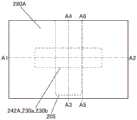
图3A、图3B、图3C及图3D是根据本发明的一个方式的晶体管200及晶体管200附近的俯视图及截面图。晶体管200对应于上述实施方式所示的晶体管20。就是说,如上述实施方式所示,可以层叠晶体管200。3A , 3B, 3C, and 3D are a plan view and a cross-sectional view of the
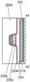
图3A是包括晶体管200的半导体装置的俯视图。此外,图3B和图3C是该半导体装置的截面图。在此,图3B是沿着图3A中的点划线A1-A2的截面图,该截面图相当于晶体管200的沟道长度方向上的截面图。此外,图3C是沿着图3A中的点划线A3-A4的截面图,该截面图相当于晶体管200的沟道宽度方向上的截面图。此外,图3D是在图3A中由点划线A5-A6表示的部分的截面图。注意,在图3A的俯视图中,为了明确起见而省略构成要素的一部分。FIG. 3A is a top view of a semiconductor device including the
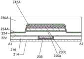
本发明的一个方式的半导体装置包括晶体管200、被用作层间膜的绝缘体214、绝缘体274、绝缘体280及绝缘体281。另外,还包括与晶体管200电连接且被用作插头的导电体240(导电体240a及导电体240b)。此外,还包括与被用作插头的导电体240的侧面接触的绝缘体241(绝缘体241a及绝缘体241b)。The semiconductor device according to one embodiment of the present invention includes a
另外,以与绝缘体254、绝缘体274及绝缘体281的开口的内壁接触的方式设置有绝缘体241,以与其侧面接触的方式设置有导电体240的第一导电体,其内侧设置有导电体240的第二导电体。在此,导电体240的顶面的高度与绝缘体281的顶面的高度可以大致相同。另外,在晶体管200中,层叠有导电体240的第一导电体与导电体240的第二导电体,但是本发明不局限于此。例如,导电体240也可以具有单层结构或者三层以上的叠层结构。另外,在结构体具有叠层结构的情况下,有时按形成顺序赋予序数以进行区別。In addition, the
[晶体管200][Transistor 200]
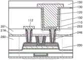
如图1所示,晶体管200包括配置在衬底(未图示)上的绝缘体214及绝缘体216、以埋入到绝缘体216中的方式配置的导电体205、配置在绝缘体216上及导电体205上的绝缘体222、配置在绝缘体222上的绝缘体224、配置在绝缘体224上的氧化物230(氧化物230a、氧化物230b、氧化物230c1及氧化物230c2)、配置在氧化物230上的绝缘体250、配置在绝缘体250上的导电体260(导电体260a及导电体260b)、接触于氧化物230b的顶面的一部分的导电体242a及导电体242b、以接触于绝缘体224的顶面的一部分、氧化物230a的侧面、氧化物230b的侧面、导电体242a的侧面、导电体242a的顶面、导电体242b的侧面及导电体242b的顶面的方式配置的绝缘体254、配置在绝缘体254上的绝缘体280以及配置在绝缘体280上的绝缘体274。导电体260包括导电体260a及导电体260b,并且以包围导电体260b的底面及侧面的方式配置导电体260a。在此,如图3B所示,导电体260的顶面以与绝缘体250的顶面、氧化物230c1的顶面、氧化物230c2的顶面以及绝缘体280的顶面大致一致的方式配置。另外,绝缘体274与导电体260、氧化物230c及绝缘体250的每一个的顶面接触。注意,下面有时将氧化物230c1和氧化物230c2一并称为氧化物230c。As shown in FIG. 1 , the
在此,绝缘体214对应于上述实施方式的晶体管20中的绝缘体30。另外,绝缘体224对应于实施方式的晶体管20中的绝缘体32。另外,氧化物230b对应于上述实施方式的晶体管20中的氧化物22a。另外,导电体242a及导电体242b对应于上述实施方式的晶体管20中的导电体28a及导电体28b。另外,绝缘体254对应于上述实施方式的晶体管20中的绝缘体34。另外,绝缘体280对应于上述实施方式的晶体管20中的绝缘体36。另外,氧化物230c对应于上述实施方式的晶体管20中的氧化物22b。另外,绝缘体250对应于上述实施方式的晶体管20中的绝缘体24。另外,导电体260对应于上述实施方式的晶体管20中的导电体26。另外,绝缘体274对应于上述实施方式的晶体管20中的绝缘体38。另外,绝缘体281对应于上述实施方式的晶体管20中的绝缘体40。此外,绝缘体222也可以对应于上述实施方式的晶体管20中的绝缘体32。Here, the
另外,绝缘体280优选具有包含通过加热脱离的氧的区域。通过将通过加热释放氧的绝缘体280以与氧化物230c1接触的方式设置,可以将绝缘体280中的氧通过氧化物230c1高效地供应到氧化物230b中。In addition, the
绝缘体222、绝缘体254及绝缘体274优选具有抑制氧(例如,氧原子、氧分子等中的至少一个)的扩散的功能。此外,绝缘体222、绝缘体254及绝缘体274优选具有抑制氢(例如,氢原子、氢分子等)中的至少一个的扩散的功能。例如,绝缘体222、绝缘体254及绝缘体274的氧和氢中的一方或双方的透过性优选都比绝缘体224低。绝缘体222、绝缘体254及绝缘体274的氧和氢中的一方或双方的透过性优选都比绝缘体250低。绝缘体222、绝缘体254及绝缘体274的氧和氢中的一方或双方的透过性优选都比绝缘体280低。The
另外,如图3B、图3C所示,绝缘体254优选与导电体242a的顶面及侧面、导电体242b的顶面及侧面、氧化物230a及氧化物230b的侧面以及绝缘体224的顶面接触。In addition, as shown in FIGS. 3B and 3C , the
通过采用上述结构,可以使用绝缘体274及氧化物230c使绝缘体280与导电体260分离。由此,可以防止包含在绝缘体280中的氧直接扩散到导电体260中。此外,可以使用氧化物230c及绝缘体254使绝缘体280与导电体242a及导电体242b分离。由此,可以防止包含在绝缘体280中的氧直接扩散到导电体242a及导电体242b中。By adopting the above structure, the
另外,氧化物230优选包括配置在绝缘体224上的氧化物230a、配置在氧化物230a上的氧化物230b、配置在氧化物230b上且其至少一部分与氧化物230b的顶面接触的氧化物230c。另外,氧化物230c也可以具有氧化物230c1与接触于氧化物230c1的顶面的氧化物230c2的叠层结构。In addition, the
注意,在此示出晶体管200具有在形成沟道的区域(以下,也称为沟道形成区域)及其附近层叠有氧化物230a、氧化物230b、氧化物230c1及氧化物230c2的四层的结构,但是本发明不局限于此。例如,也可以具有氧化物230b的单层结构、氧化物230b与氧化物230a的两层结构、氧化物230b与氧化物230c2的两层结构、氧化物230a、氧化物230b及氧化物230c1的三层结构或者五层以上的叠层结构。另外,在晶体管200中,导电体260具有两层的叠层结构,但是本发明不局限于此。例如,导电体260也可以具有单层结构或三层以上的叠层结构。Note that the
在此,导电体260被用作晶体管的栅电极,导电体242a及导电体242b被用作源电极或漏电极。在晶体管200中,以填埋由绝缘体280等形成的开口的方式自对准地形成被用作栅电极的导电体260。通过如此形成导电体260,可以在导电体242a和导电体242b之间的区域中无需对准并确实地配置导电体260。另外,如图1所示,导电体260优选包括导电体260a、配置在导电体260a上的导电体260b。Here, the
此外,晶体管200优选包括配置在衬底(未图示)上的绝缘体214、配置在绝缘体214上的绝缘体216、以填埋于绝缘体214及绝缘体216中的方式配置的导电体205以及配置在绝缘体216及导电体205上的绝缘体222。再者,优选在绝缘体222上配置有绝缘体224。In addition, the
另外,优选在晶体管200中将被用作氧化物半导体的金属氧化物(以下,也称为氧化物半导体)用于包含沟道形成区域的氧化物230(氧化物230a、氧化物230b、氧化物230c1及氧化物230c2)。In addition, in the
由于将氧化物半导体用于沟道形成区域的晶体管200在非导通状态下的泄漏电流(关态电流)极小,所以可以提供低功耗的半导体装置。此外,由于氧化物半导体可以利用溅射法等形成,所以可以用于构成高集成型半导体装置的晶体管200。Since the leakage current (off-state current) in the non-conductive state of the
作为氧化物230优选使用In-M-Zn氧化物(元素M为选自铝、镓、钇、锡、铜、钒、铍、硼、钛、铁、镍、锗、锆、钼、镧、铈、钕、铪、钽、钨和镁等中的一种或多种)等金属氧化物。特别是,作为元素M可以使用铝、镓、钇或锡。此外,作为氧化物230也可以使用In-Ga氧化物、In-Zn氧化物。In-M-Zn oxide is preferably used as the oxide 230 (the element M is selected from the group consisting of aluminum, gallium, yttrium, tin, copper, vanadium, beryllium, boron, titanium, iron, nickel, germanium, zirconium, molybdenum, lanthanum, cerium , one or more of neodymium, hafnium, tantalum, tungsten and magnesium) and other metal oxides. In particular, as the element M, aluminum, gallium, yttrium or tin can be used. In addition, In-Ga oxide and In-Zn oxide can also be used as the
此外,在使用氧化物半导体的晶体管中,如果氧化物半导体中的形成沟道的区域中存在杂质及氧空位,电特性则容易变动,有时降低可靠性。另外,在氧化物半导体中的形成沟道的区域中包含氧空位的情况下,晶体管趋于具有常开启特性。因此,优选为尽可能降低形成沟道的区域中的氧空位。例如,通过氧化物230c等对氧化物230b供应氧,填充氧空位,即可。由此,抑制电特性的变动,从而可以提供具有稳定的电特性且可靠性得到提高的晶体管。In addition, in a transistor using an oxide semiconductor, if impurities and oxygen vacancies exist in a region where a channel is formed in the oxide semiconductor, electrical characteristics are likely to vary, and reliability may be lowered. In addition, in the case where oxygen vacancies are contained in the region where the channel is formed in the oxide semiconductor, the transistor tends to have normally-on characteristics. Therefore, it is preferable to reduce the oxygen vacancies in the region where the channel is formed as much as possible. For example, oxygen vacancies may be filled by supplying oxygen to the
另外,在包含在以与氧化物230上接触的方式设置并被用作源电极或漏电极的导电体242(导电体242a及导电体242b)中的元素(例如,第二元素)具有吸收氧化物230的氧的功能的情况下,可能在氧化物230和导电体242之间或氧化物230的表面附近部分地形成低电阻区域。在此情况下,在该低电阻区域中,进入氧空位的杂质(氢、氮或金属元素等)被用作供体,载流子密度会增高。另外,下面有时将进入氧空位的氢称为VOH。In addition, the element (for example, the second element) contained in the conductor 242 (the
此外,图4A示出图3B所示的晶体管200的一部分的区域的放大图。如图4A所示,有时以与氧化物230上接触的方式设置有导电体242,在氧化物230的与导电体242的界面及其附近作为低电阻区域形成有区域243(区域243a及区域243b)。氧化物230包括被用作晶体管200的沟道形成区域的区域234、包括区域243的一部分且被用作源区域或漏区域的区域231(区域231a及区域231b)。另外,在下面的附图中,有时即使在放大图等中没有示出区域243也形成有同样的区域243。In addition, FIG. 4A shows an enlarged view of a region of a part of the
另外,虽然示出了在氧化物230b的导电体242附近,区域243a及区域243b以在深度方向上扩散的方式设置的例子,但是本发明不局限于此。区域243a及区域243b根据所需要的晶体管的电特性适当地形成,即可。在氧化物230中,有时难以明确地观察各区域的边界。在各区域中检测出的元素的浓度不仅限于按每区域分阶段地变化,也可以在各区域中逐渐地变化。In addition, although the example in which the area|
如图4A所示,在本发明的一个方式的晶体管200中,绝缘体274的底面与氧化物230c的顶面接触,导电体260与绝缘体280分离。由此,可以防止绝缘体280所包含的氧被导电体260吸收。另外,如图4A所示,在本发明的一个方式的晶体管200中,氧化物230c的侧面与绝缘体254的侧面接触,导电体242a及导电体242b与绝缘体280分离。由此,可以防止绝缘体280所包含的氧被导电体242a及导电体242b吸收。As shown in FIG. 4A , in the
在此,图4B示出图3C所示的晶体管200的一部分的区域的放大图。图4B是晶体管200的W宽度方向上的沟道形成区域的放大图。Here, FIG. 4B shows an enlarged view of a region of a part of the
如图4B所示,以绝缘体224的底面为标准,氧化物230a及氧化物230b和导电体260不重叠的区域中的导电体260的底面的高度优选比氧化物230b的底面的高度低。此外,在氧化物230b和导电体260不重叠的区域中的导电体260的底面的高度和氧化物230b的底面的高度之间的差异为T2时,T2为0nm以上且100nm以下,优选为3nm以上且50nm以下,更优选为5nm以上且20nm以下。As shown in FIG. 4B , based on the bottom surface of the
如此,采用被用作栅电极的导电体260隔着氧化物230c及绝缘体250覆盖沟道形成区域的氧化物230b的侧面及顶面的结构,该结构容易使导电体260的电场作用于沟道形成区域的氧化物230b整体。因此,可以增大晶体管200的通态电流并提高频率特性。In this way, a structure in which the
如上所述,可以提供包括通态电流大的晶体管的半导体装置。另外,可以提供包括具有高频率特性的晶体管的半导体装置。另外,可以提供抑制电特性变动而实现具有稳定的电特性并提高了可靠性的半导体装置。另外,可以提供包括关态电流小的晶体管的半导体装置。As described above, a semiconductor device including a transistor with a large on-state current can be provided. In addition, a semiconductor device including a transistor having high frequency characteristics can be provided. In addition, it is possible to provide a semiconductor device having stable electrical properties and improved reliability by suppressing fluctuations in electrical properties. In addition, a semiconductor device including a transistor with a small off-state current can be provided.
下面,说明包括本发明的一个方式的晶体管200的半导体装置的详细结构。Next, a detailed configuration of a semiconductor device including the
导电体205以与氧化物230及导电体260重叠的方式配置。另外,导电体205优选以填埋于绝缘体214及绝缘体216中的方式设置。在此,导电体205的顶面的平坦性优选为高。例如,导电体205的顶面的平均表面粗糙度(Ra)为1nm以下,优选为0.5nm以下,更优选为0.3nm以下即可。由此,可以使形成在导电体205上的绝缘体224的平坦性良好且提高氧化物230b及氧化物230c的结晶性。The
在此,导电体260有时被用作第一栅(也称为顶栅极)电极。此外,导电体205有时被用作第二栅(也称为底栅极)电极。在此情况下,通过独立地改变施加到导电体205中的电位而不使其与施加到导电体260中的电位联动,可以控制晶体管200的Vth。尤其是,通过对导电体205施加负电位,可以使晶体管200的Vth大于0V且可以减小关态电流。因此,与不对导电体205施加负电位时相比,在对导电体205施加负电位的情况下,可以减小对导电体260施加的电位为0V时的漏极电流。Here, the
另外,如图3A所示,导电体205优选比氧化物230中的区域234大。尤其是,如图3C所示,导电体205优选延伸到与沟道宽度方向交叉的氧化物230中的区域234的端部的外侧的区域。就是说,优选在氧化物230的沟道宽度方向的侧面的外侧,导电体205和导电体260隔着绝缘体重叠。In addition, as shown in FIG. 3A , the
通过具有上述结构,可以由被用作第一栅电极的导电体260的电场和被用作第二栅电极的导电体205的电场电围绕区域234中的沟道形成区域。By having the above-described structure, the channel formation region in the
此外,如图3C所示,将导电体205延伸来被用作布线。但是,本发明不局限于此,也可以在导电体205下设置被用作布线的导电体。此外,不一定需要在每一个晶体管中设置一个导电体205。例如,在多个晶体管中可以共同使用导电体205。Further, as shown in FIG. 3C , the
另外,在导电体205中,以与绝缘体216的开口的内壁接触的方式形成有第一导电体,其内侧形成有第二导电体。在此,导电体205的第一导电体及第二导电体的高度与绝缘体216的顶面的高度可以大致相同。虽然在晶体管200中层叠有导电体205的第一导电体与第二导电体,但是本发明不局限于此。例如,导电体205也可以具有单层结构或者三层以上的叠层结构。在结构体具有叠层结构的情况下,有时按形成顺序赋予序数以进行区別。In addition, in the
此外,也可以作为导电体205的第一导电体使用具有抑制氢原子、氢分子、水分子、氮原子、氮分子、氧化氮分子(N2O、NO、NO2等)、铜原子等杂质的扩散的功能(不容易使上述杂质透过)的导电体。此外,优选使用具有抑制氧(例如,氧原子、氧分子等中的至少一个)的扩散的功能(不容易使上述氧透过)的导电体。在本说明书中,“抑制杂质或氧的扩散的功能”是指抑制上述杂质和上述氧中的任一个或全部的扩散的功能。In addition, impurities containing suppressed hydrogen atoms, hydrogen molecules, water molecules, nitrogen atoms, nitrogen molecules, nitrogen oxide molecules (N2 O, NO, NO2 , etc.), and copper atoms can also be used as the first conductor of the
当作为导电体205的第一导电体使用具有抑制氧的扩散的功能的导电体时,可以抑制导电体205被氧化而导致导电率的下降。作为具有抑制氧的扩散的功能的导电体,例如,优选使用钽、氮化钽、钌或氧化钌等。因此,作为导电体205的第一导电体,可以使用上述导电材料的单层或叠层。When an electrical conductor having a function of suppressing the diffusion of oxygen is used as the first electrical conductor of the
此外,作为导电体205的第二导电体,优选使用以钨、铜或铝为主要成分的导电材料。Further, as the second conductor of the
绝缘体214优选使用具有抑制氧(例如,氧原子、氧分子等)的扩散(不容易使上述氧透过)的功能的绝缘材料。另外,绝缘体214优选被用作抑制水或氢等杂质从衬底一侧进入晶体管200的阻挡绝缘膜。因此,作为绝缘体214优选使用具有抑制氢原子、氢分子、水分子、氮原子、氮分子、氧化氮分子(N2O、NO、NO2等)、铜原子等杂质的扩散的功能(不容易使上述杂质透过)的绝缘材料。As the
例如,作为绝缘体214,优选使用氮化硅等。由此,可以抑制水或氢等杂质从与绝缘体214相比更靠近衬底一侧扩散到晶体管200一侧。此外,可以抑制包含在绝缘体224等中的氧扩散到与绝缘体214相比更靠近衬底一侧。另外,作为绝缘体222也可以使用作为绝缘材料的包含铝和铪中的一方或双方的氧化物的绝缘体。For example, as the
此外,绝缘体216、绝缘体280及绝缘体281的介电常数优选比绝缘体214低。通过将介电常数低的材料作为层间膜,可以减少产生在布线之间的寄生电容。例如,作为绝缘体216、绝缘体280及绝缘体281,适当地使用氧化硅、氧氮化硅、氮氧化硅、氮化硅、添加有氟的氧化硅、添加有碳的氧化硅、添加有碳及氮的氧化硅或具有空孔的氧化硅等即可。Further, the dielectric constants of the
绝缘体222及绝缘体224被用作栅极绝缘体。The
在此,在与氧化物230接触的绝缘体224中,优选通过加热使氧脱离。在本说明书中,有时将通过加热脱离的氧称为过剩氧。例如,作为绝缘体224适当地使用氧化硅或氧氮化硅等,即可。通过以与氧化物230接触的方式设置上述包含过剩氧的绝缘体,可以减少氧化物230中的氧空位,从而可以提高晶体管200的可靠性。Here, in the
具体而言,作为绝缘体224,优选使用通过加热使一部分的氧脱离的氧化物材料。通过加热使氧脱离的氧化物是指在TDS(Thermal Desorption Spectroscopy:热脱附谱)分析中换算为氧原子的氧的脱离量为1.0×10¹⁸atoms/cm3以上,优选为1.0×1019atoms/cm3以上,进一步优选为2.0×1019atoms/cm3以上,或者3.0×1020atoms/cm3以上的氧化物膜。另外,进行上述TDS分析时的膜的表面温度优选在100℃以上且700℃以下,或者100℃以上且400℃以下的范围内。Specifically, as the
此外,如图3C所示,有时在绝缘体224中不与绝缘体254重叠并不与氧化物230b重叠的区域的厚度比其他区域的厚度薄。在绝缘体224中,不与绝缘体254重叠并不与氧化物230b重叠的区域优选具有足够使上述氧扩散的厚度。Furthermore, as shown in FIG. 3C , the thickness of a region of the
绝缘体222优选具有抑制氧(例如,氧原子、氧分子等中的至少一个)的扩散的功能(不容易使上述氧透过)。例如,绝缘体222的氧透过性优选比绝缘体224低。通过使绝缘体222具有抑制氧或杂质的扩散的功能,可以减少氧化物230所具有的氧能够扩散到绝缘体220一侧,所以是优选的。此外,可以抑制导电体205与绝缘体224及氧化物230所具有的氧起反应。The
再者,绝缘体222优选被用作抑制水或氢等杂质从衬底一侧混入晶体管200的阻挡绝缘膜。例如,绝缘体222的氢透过性优选比绝缘体224低。通过由绝缘体222及绝缘体254围绕绝缘体224及氧化物230等,可以抑制水或氢等杂质从外部进入晶体管200。Furthermore, the
绝缘体222使用作为绝缘材料的包含铝和铪中的一方或双方的氧化物的绝缘体即可。作为包含铝和铪中的一方或双方的氧化物的绝缘体,优选使用氧化铝、氧化铪、包含铝及铪的氧化物(铝酸铪)等。当使用这种材料形成绝缘体222时,绝缘体222被用作抑制氧从氧化物230释放或氢等杂质从晶体管200的周围部进入氧化物230的层。As the
或者,例如也可以对上述绝缘体添加氧化铝、氧化铋、氧化锗、氧化铌、氧化硅、氧化钛、氧化钨、氧化钇、氧化锆。此外,也可以对上述绝缘体进行氮化处理。还可以在上述绝缘体上层叠氧化硅、氧氮化硅或氮化硅。Alternatively, for example, aluminum oxide, bismuth oxide, germanium oxide, niobium oxide, silicon oxide, titanium oxide, tungsten oxide, yttrium oxide, and zirconium oxide may be added to the insulator. In addition, the above-mentioned insulator may be subjected to nitridation treatment. Silicon oxide, silicon oxynitride, or silicon nitride may also be stacked on the above-mentioned insulator.
此外,作为绝缘体222,例如也可以以单层或叠层使用包含氧化铝、氧化铪、氧化钽、氧化锆、锆钛酸铅(PZT)、钛酸锶(SrTiO3)或(Ba,Sr)TiO3(BST)等所谓的high-k材料的绝缘体。当进行晶体管的微型化及高集成化时,由于栅极绝缘体的薄膜化,有时发生泄漏电流等问题。通过作为被用作栅极绝缘体的绝缘体使用high-k材料,可以在保持物理厚度的同时降低晶体管工作时的栅极电位。In addition, as the
另外,绝缘体222及绝缘体224也可以具有两层以上的叠层结构。此时,不局限于使用相同材料构成的叠层结构,也可以是使用不同材料构成的叠层结构。In addition, the
氧化物230包括氧化物230a、氧化物230a上的氧化物230b及氧化物230b上的氧化物230c。当在氧化物230b下设置有氧化物230a时,可以抑制杂质从形成在氧化物230a下的结构物扩散到氧化物230b中。当在氧化物230b上设置有氧化物230c时,可以抑制杂质从形成在氧化物230c的上方的结构物扩散到氧化物230b中。
另外,如图3等所示,氧化物230c优选包括氧化物230c1及配置在氧化物230c1上的氧化物230c2。氧化物230c1优选包括构成用于氧化物230b的金属氧化物的金属元素中的至少一个,更优选包括所有上述金属元素。由此,可以降低氧化物230b与氧化物230c1的界面的缺陷态密度。Moreover, as shown in FIG. 3 etc., it is preferable that the oxide 230c contains the oxide 230c1 and the oxide 230c2 arrange|positioned on the oxide 230c1. The oxide 230c1 preferably includes at least one of the metal elements constituting the metal oxide used for the
另外,氧化物230优选具有各金属原子的原子个数比互不相同的氧化物的叠层结构。具体而言,在用于氧化物230a的金属氧化物中,构成元素中的元素M的原子个数比优选大于用于氧化物230b的金属氧化物的构成元素中的元素M的原子个数比。另外,在用于氧化物230a的金属氧化物中,相对于In的元素M的原子个数比优选大于用于氧化物230b的金属氧化物中的相对于In的元素M的原子个数比。另外,在用于氧化物230b的金属氧化物中,相对于元素M的In的原子个数比优选大于用于氧化物230a的金属氧化物中的相对于元素M的In的原子个数比。另外,氧化物230c可以使用可用于氧化物230a或氧化物230b的金属氧化物。另外,当采用氧化物230c1与氧化物230c2的叠层结构时,在用于氧化物230c2的金属氧化物中,通过使构成元素中的In的原子个数比小于用于氧化物230c1的金属氧化物的构成元素中的In的原子个数比,可以抑制In扩散到绝缘体250一侧。In addition, the
另外,氧化物230b优选具有结晶性。例如,优选使用CAAC-OS。CAAC-OS等的具有结晶性的氧化物具有杂质及缺陷(氧空位等)少的结晶性高且致密的结构。因此,可以抑制由源电极或漏电极氧从氧化物230b被抽出。因此,即使进行加热处理也可以抑制氧从氧化物230b被抽出,所以晶体管200对制造工序中的高温度或热积存也很稳定。In addition, the
另外,氧化物230c1及氧化物230c2优选具有结晶性,例如优选使用CAAC-OS。In addition, the oxide 230c1 and the oxide 230c2 preferably have crystallinity, and for example, CAAC-OS is preferably used.
另外,优选的是,使氧化物230a及氧化物230c2的导带底的能量高于氧化物230b的导带底的能量。换言之,氧化物230a及氧化物230c2的电子亲和势优选小于氧化物230b的电子亲和势。In addition, it is preferable to make the energy of the conduction band bottom of the
在此,在氧化物230a、氧化物230b及氧化物230c的接合部中,导带底的能级平缓地变化。换言之,也可以将上述情况表达为氧化物230a、氧化物230b及氧化物230c的接合部的导带底的能级连续地变化或者连续地接合。为此,优选降低形成在氧化物230a与氧化物230b的界面以及氧化物230b与氧化物230c的界面的混合层的缺陷态密度。Here, in the junction of the
具体而言,作为氧化物230a使用In:Ga:Zn=1:3:4[原子个数比]或1:1:0.5[原子个数比]的金属氧化物,即可。此外,作为氧化物230b使用In:Ga:Zn=4:2:3[原子个数比]或3:1:2[原子个数比]的金属氧化物,即可。此外,作为氧化物230c使用In:Ga:Zn=1:3:4[原子个数比]、In:Ga:Zn=4:2:3[原子个数比]、Ga:Zn=2:1[原子个数比]或Ga:Zn=2:5[原子个数比]的金属氧化物,即可。此外,作为氧化物230c1与氧化物230c2的组合的具体例子,可以举出In:Ga:Zn=4:2:3[原子个数比]和In:Ga:Zn=1:3:4[原子个数比]的叠层结构、In:Ga:Zn=4:2:3[原子个数比]和Ga:Zn=2:1[原子个数比]的叠层结构、In:Ga:Zn=4:2:3[原子个数比]和Ga:Zn=2:5[原子个数比]的叠层结构、In:Ga:Zn=4:2:3[原子个数比]和氧化镓的叠层结构等。Specifically, it is sufficient to use a metal oxide of In:Ga:Zn=1:3:4 [atomic ratio] or 1:1:0.5 [atomic ratio] as the
此时,载流子的主要路径为氧化物230b。通过使氧化物230a及氧化物230c具有上述结构,可以降低氧化物230a与氧化物230b的界面及氧化物230b与氧化物230c的界面的缺陷态密度。因此,界面散射对载流子传导带来的影响减少,从而晶体管200可以得到高通态电流及高频率特性。At this time, the main path of the carriers is the
作为氧化物230优选使用被用作氧化物半导体的金属氧化物。例如,作为成为区域234的金属氧化物,优选使用其带隙为2eV以上,优选为2.5eV以上的金属氧化物。如此,通过使用带隙较宽的金属氧化物,可以减小晶体管的关态电流。通过采用这种晶体管,可以提供低功耗的半导体装置。As the
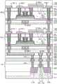
在此,参照图5及图6说明对根据本实施方式的晶体管200进行加热处理时的包含在绝缘体280中的氧290的举动。图5是晶体管200的沟道长度方向上的放大截面图,图6是晶体管200的沟道宽度方向上的放大截面图。如上所述,在本实施方式所示的半导体装置中,含有过剩氧的绝缘体280由绝缘体274、氧化物230c1、氧化物230c2及绝缘体254围绕并与导电体260、导电体242a及导电体242b分离。由此,如图5及图6所示,即使进行加热处理,绝缘体280中的氧290也被绝缘体274、氧化物230c1、氧化物230c2及绝缘体254阻挡而不直接扩散到导电体260、导电体242a及导电体242b中。Here, the behavior of the
另外,当通过加热处理使氧化物230b中的氧脱离而形成氧空位时,在氧化物230b与氧化物230c1的界面附近从氧化物230c1到氧化物230b扩散氧,由此填充氧空位。供应到氧化物230b中的氧在氧化物230b中反复地填充氧空位的同时扩散在氧化物230b中。In addition, when oxygen vacancies are formed by desorbing oxygen in the
另外,通过对氧化物230b供应氧,在氧化物230c1中也形成氧空位。此时,在绝缘体280与氧化物230c1的界面附近从绝缘体280到氧化物230c1中扩散氧290,由此填充氧空位。供应到氧化物230c1中的氧290在氧化物230c中反复地填充氧空位的同时扩散在氧化物230c1中。注意,如图5及图6所示,有时氧化物230c1中的氧290扩散到氧化物230c2中而通过氧化物230c2供应到氧化物230b中。In addition, oxygen vacancies are also formed in the oxide 230c1 by supplying oxygen to the
在此,氧化物230c1优选为CAAC-OS。如图5及图6所示,氧化物230c1包括具有在a-b面方向延伸的结晶层230c1P及垂直于a-b面方向的c轴230c1X的结晶区域。在此,在氧化物230c1中,c轴230c1X优选沿大致垂直于氧化物230c1的被形成面的方向取向。由此,氧化物230c1包括c轴230c1X沿大致垂直于氧化物230b的顶面的方向取向的区域、c轴230c1X沿大致垂直于导电体242a、绝缘体254及绝缘体280的侧面的方向取向的区域以及c轴230c1X以大致垂直于导电体242b、绝缘体254及绝缘体280的侧面的方向取向的区域。此外,与氧化物230c1同样,氧化物230c2也是CAAC-OS,如图5及图6所示,该氧化物230c2也可以包括具有在a-b面方向延伸的结晶层230c2P及垂直于a-b面方向的c轴230c2X的结晶区域。Here, the oxide 230c1 is preferably CAAC-OS. As shown in FIGS. 5 and 6 , the oxide 230c1 includes a crystal layer 230c1P extending in the a-b plane direction and a crystal region having a c-axis 230c1X perpendicular to the a-b plane direction. Here, in the oxide 230c1, the c-axis 230c1X is preferably oriented in a direction substantially perpendicular to the surface on which the oxide 230c1 is formed. Thus, oxide 230c1 includes regions with c-axis 230c1X oriented in a direction substantially perpendicular to the top surface of
CAAC-OS具有与c軸方向相比在a-b面方向更容易使氧扩散的性质。因此,如图5所示,从绝缘体280供应到氧化物230c1及氧化物230c2中的氧290优先地扩散到氧化物230c1与氧化物230b的界面附近,而可以填充氧化物230c中的氧空位。CAAC-OS has a property that oxygen is more easily diffused in the a-b plane direction than in the c-axis direction. Therefore, as shown in FIG. 5 , the
如上所述,本实施方式所示的晶体管200即使完成后进行加热处理也通过从绝缘体280对氧化物230中供应氧而可以抑制在氧化物230中增加氧空位。因此,在叠层结构的下层中也可以在抑制晶体管200的电特性的变动而具有稳定的电特性的同时提高晶体管200的可靠性。As described above, the
注意,虽然图5及图6示出氧290在氧化物230c1及氧化物230c2中扩散的例子,但是本实施方式不局限于此。例如,也可以采用氧290只在氧化物230c1中扩散而氧化物230c2防止氧290的扩散的结构。通过采用该结构,可以更降低氧290被导电体260吸收。Note that although FIGS. 5 and 6 show an example in which the
在氧化物230b上设置被用作源电极及漏电极的导电体242(导电体242a及导电体242b)。导电体242的厚度例如为1nm以上且50nm以下,优选为2nm以上且25nm以下,即可。Conductors 242 (
作为导电体242,优选使用选自铝、铬、铜、银、金、铂、钽、镍、钛、钼、钨、铪、钒、铌、锰、镁、锆、铍、铟、钌、铱、锶和镧中的金属元素、以上述金属元素为成分的合金或者组合上述金属元素的合金等。例如,优选使用氮化钽、氮化钛、钨、包含钛和铝的氮化物、包含钽和铝的氮化物、氧化钌、氮化钌、包含锶和钌的氧化物、包含镧和镍的氧化物等。另外,氮化钽、氮化钛、包含钛和铝的氮化物、包含钽和铝的氮化物、氧化钌、氮化钌、包含锶和钌的氧化物、包含镧和镍的氧化物是不容易氧化的导电材料或者吸收氧也维持导电性的材料,所以是优选的。As the
与绝缘体222等同样,绝缘体254优选具有抑制氧(例如,氧原子、氧分子等)的扩散的功能(不容易使上述氧透过)。例如,绝缘体254的氧透过性优选低于绝缘体224。再者,如图3B、图3C所示,绝缘体254优选与导电体242a的顶面及侧面、导电体242b的顶面及侧面、氧化物230a及氧化物230b的侧面以及绝缘体224的顶面接触。通过采用上述结构,可以抑制包含在绝缘体280中的氧被导电体242a及导电体242b吸收。Like the
另外,如图3D所示,氧化物230a及氧化物230b的到与导电体242b(导电体242a)重叠的区域的沟道宽度方向一侧的侧面也被绝缘体254覆盖。通过采用上述结构,可以进一步防止绝缘体280所包含的氧被导电体242a及导电体242b吸收。In addition, as shown in FIG. 3D , the side surfaces of the
再者,优选被用作抑制水或氢等杂质从绝缘体280一侧混入晶体管200的阻挡绝缘膜。例如,绝缘体254的氢透过性优选比绝缘体224低。Furthermore, it is preferably used as a blocking insulating film for preventing impurities such as water and hydrogen from being mixed into the
绝缘体254优选通过溅射法形成。通过在包含氧的气氛下使用溅射法形成绝缘体254,可以对绝缘体224与绝缘体254接触的区域附近添加氧。由此,可以将氧从该区域通过绝缘体224供应到氧化物230中。在此,通过使绝缘体254具有抑制扩散到上方的氧的功能,可以防止氧从氧化物230扩散到绝缘体280中。此外,通过使绝缘体222具有抑制扩散到下方的氧的功能,可以防止氧从氧化物230扩散到绝缘体216中。如此,对氧化物230中的被用作沟道形成区域的区域234供应氧。由此,可以减少氧化物230的氧空位并抑制晶体管的常开启化。The
此外,绝缘体254可以具有两层以上的多层结构。例如,作为绝缘体254,可以在包含氧的气氛下使用溅射法形成第一层,然后使用ALD法形成第二层,来形成两层结构。因为ALD法是覆盖性良好的成膜方法,所以可以防止因第一层的凹凸而产生断开等。In addition, the
作为绝缘体254,例如可以形成包含铝和铪中的一方或双方的氧化物的绝缘体。注意,作为包含铝和铪中的一方或双方的氧化物的绝缘体,优选使用氧化铝、氧化铪、包含铝及铪的氧化物(铝酸铪)等。另外,作为绝缘体254也可以使用氮化硅等阻挡性高的氮化物。As the
绝缘体250被用作栅极绝缘体。绝缘体250优选与氧化物230c的顶面接触地配置。绝缘体250可以使用氧化硅、氧氮化硅、氮氧化硅、氮化硅、添加有氟的氧化硅、添加有碳的氧化硅、添加有碳及氮的氧化硅、具有空孔的氧化硅。尤其是,氧化硅及氧氮化硅具有热稳定性,所以是优选的。The
与绝缘体224同样地,绝缘体250优选使用通过加热释放氧的绝缘体形成。通过作为绝缘体250以与氧化物230c的顶面接触的方式设置通过加热释放氧的绝缘体,可以高效地对氧化物230b的区域234供应氧。与绝缘体224同样,优选降低绝缘体250中的水或氢等杂质的浓度。绝缘体250的厚度优选为1nm以上且20nm以下。Like the
另外,也可以在绝缘体250与导电体260之间设置金属氧化物。该金属氧化物优选抑制从绝缘体250扩散到导电体260中的氧。通过设置抑制氧的扩散的金属氧化物,从绝缘体250扩散到导电体260中的氧被抑制。换言之,可以抑制供应到氧化物230中的氧量的减少。另外,可以抑制因绝缘体250中的氧所导致的导电体260的氧化。In addition, a metal oxide may be provided between the
另外,该金属氧化物有时被用作栅极绝缘体的一部分。因此,在将氧化硅或氧氮化硅等用于绝缘体250的情况下,作为该金属氧化物优选使用作为相对介电常数高的high-k材料的金属氧化物。通过使栅极绝缘体具有绝缘体250与该金属氧化物的叠层结构,可以形成具有热稳定性且相对介电常数高的叠层结构。因此,可以在保持栅极绝缘体的物理厚度的同时降低在晶体管工作时施加的栅极电位。另外,可以减少被用作栅极绝缘体的绝缘体的等效氧化物厚度(EOT)。In addition, the metal oxide is sometimes used as part of the gate insulator. Therefore, when silicon oxide, silicon oxynitride, or the like is used for the
具体而言,可以使用包含选自铪、铝、镓、钇、锆、钨、钛、钽、镍、锗和镁等中的一种或两种以上的金属氧化物。特别是,优选使用作为包含铝和铪中的一方或双方的氧化物的绝缘体的氧化铝、氧化铪、包含铝及铪的氧化物(铝酸铪)等。Specifically, a metal oxide containing one or two or more selected from hafnium, aluminum, gallium, yttrium, zirconium, tungsten, titanium, tantalum, nickel, germanium, magnesium, and the like can be used. In particular, alumina, hafnium oxide, oxides containing aluminum and hafnium (hafnium aluminate), etc., which are insulators containing oxides of one or both of aluminum and hafnium, are preferably used.
虽然在图1中,导电体260具有两层结构,但是也可以具有单层结构或三层以上的叠层结构。Although the
作为导电体260a优选使用具有抑制氢原子、氢分子、水分子、氮原子、氮分子、氧化氮分子(N2O、NO、NO2等)、铜原子等杂质的扩散的功能的导电材料。另外,优选使用具有抑制氧(例如,氧原子、氧分子等中的至少一个)的扩散的功能的导电材料。As the
此外,当导电体260a具有抑制氧的扩散的功能时,可以抑制绝缘体250所包含的氧使导电体260b氧化而导致导电率的下降。作为具有抑制氧的扩散的功能的导电材料,例如,优选使用钽、氮化钽、钌或氧化钌等。In addition, when the
此外,作为导电体260b优选使用以钨、铜或铝为主要成分的导电材料。另外,由于导电体260还被用作布线,所以优选使用导电性高的导电体。例如,可以使用以钨、铜或铝为主要成分的导电材料。另外,导电体260b可以具有叠层结构,例如可以具有钛、氮化钛与上述导电材料的叠层结构。In addition, it is preferable to use a conductive material mainly composed of tungsten, copper, or aluminum as the
绝缘体280优选隔着绝缘体254设置在绝缘体224、氧化物230及导电体242上。绝缘体280优选包含通过加热脱离的氧。例如,作为绝缘体280,优选具有氧化硅、氧氮化硅、氮氧化硅、添加有氟的氧化硅、添加有碳的氧化硅、添加有碳及氮的氧化硅或具有空孔的氧化硅等。尤其是,氧化硅及氧氮化硅具有热稳定性,所以是优选的。特别是,因为氧化硅、氧氮化硅、具有空孔的氧化硅等的材料容易形成包含通过加热脱离的氧的区域,所以是优选的。The
另外,优选绝缘体280中的水或氢等杂质的浓度得到降低。此外,绝缘体280的顶面也可以被平坦化。In addition, the concentration of impurities such as water and hydrogen in the
绝缘体274优选与绝缘体210等同样地被用作抑制水或氢等杂质从上方混入到绝缘体280中的阻挡绝缘膜。作为绝缘体274,例如可以使用能够用于绝缘体210、绝缘体254等的绝缘体。The
绝缘体274优选与绝缘体222等同样地具有抑制氧(例如,氧原子、氧分子等)的拡散的功能(不容易使上述氧透过)。例如,绝缘体274的氧透过性优选低于绝缘体280。再者,如图3B及图3C所示,绝缘体274优选接触于导电体260的顶面、绝缘体250的顶面、氧化物230c的顶面及绝缘体280的顶面。通过采用上述结构,可以进一步防止绝缘体280所包含的氧被导电体260吸收。The
再者,绝缘体274优选被用作抑制水、氢等杂质从绝缘体281一侧混入晶体管200的阻挡绝缘膜。例如,绝缘体274的氢透过性优选比绝缘体280低。Furthermore, the
绝缘体274优选通过溅射法形成。绝缘体274优选在包含氧的气氛下利用溅射法形成。通过使用溅射法形成绝缘体274,可以对绝缘体280的与绝缘体274接触的区域附近添加过剩氧。由此,可以将氧从该区域通过氧化物230c供应到氧化物230b中。在此,通过使绝缘体274具有抑制氧向上方扩散的功能,可以防止氧向绝缘体280的上方扩散。此外,通过使绝缘体254具有抑制氧扩散到下方的功能,可以防止氧从绝缘体280扩散到下方。如此,对氧化物230b中的被用作沟道形成区域的区域234供应氧。由此,可以减少氧化物230b的氧空位并抑制晶体管的常开启化。The
另外,优选在绝缘体274上设置被用作层间膜的绝缘体281。与绝缘体224等同样,优选绝缘体281中的水、氢等杂质的浓度得到降低。In addition, it is preferable to provide an
另外,在形成于绝缘体281、绝缘体274、绝缘体280及绝缘体254中的开口中配置导电体240a及导电体240b。导电体240a及导电体240b以中间夹着导电体260的方式设置。另外,导电体240a及导电体240b的顶面的高度与绝缘体281的顶面可以位于同一平面上。In addition, the
另外,以与绝缘体281、绝缘体274、绝缘体280及绝缘体254的开口的内壁接触的方式设置有绝缘体241a,以与其侧面接触的方式形成有导电体240a的第一导电体。导电体242a位于该开口的底部的至少一部分,导电体240a与导电体242a接触。同样,以与绝缘体281、绝缘体274、绝缘体280及绝缘体254的开口的内壁接触的方式设置有绝缘体241b,以与其侧面接触的方式形成有导电体240b的第一导电体。导电体242b位于该开口的底部的至少一部分,导电体240b与导电体242b接触。In addition, the
导电体240a及导电体240b优选使用以钨、铜或铝为主要成分的导电材料。此外,导电体240a及导电体240b也可以具有叠层结构。As the
当作为导电体240采用叠层结构时,作为与氧化物230a、氧化物230b、导电体242、绝缘体254、绝缘体280、绝缘体274及绝缘体281接触的导电体优选使用具有抑制水或氢等杂质的透过的功能的导电材料。例如,优选使用钽、氮化钽、钛、氮化钛、钌或氧化钌等。另外,也可以以单层或叠层使用具有抑制水或氢等杂质的透过的功能的导电材料。通过使用该导电材料,可以防止添加到绝缘体280的氧被吸收到导电体240a及导电体240b中。此外,可以防止水或氢等杂质从绝缘体281的上方的层通过导电体240a及导电体240b进入氧化物230。When a laminated structure is used as the conductor 240 , it is preferable to use a conductor which is in contact with the
作为绝缘体241a及绝缘体241b,使用能够用于绝缘体254等的绝缘体(例如,氧化铝或氮化硅等),即可。因为绝缘体241a及绝缘体241b与绝缘体254接触地设置,所以可以抑制从绝缘体280等水或氢等杂质经过导电体240a及导电体240b混入氧化物230。此外,可以防止绝缘体280所包含的氧被导电体240a及导电体240b吸收。As the
虽然未图示,但是也可以以与导电体240a的顶面及导电体240b的顶面接触的方式配置被用作布线的导电体。被用作布线的导电体优选使用以钨、铜或铝为主要成分的导电材料。另外,该导电体可以具有叠层结构,例如,可以具有钛、氮化钛与上述导电材料的叠层结构。另外,该导电体可以填埋于绝缘体的开口中。Although not shown, the conductors used as wirings may be arranged so as to be in contact with the top surfaces of the
〈半导体装置的构成材料〉<Constituent materials of semiconductor devices>
以下,说明可用于半导体装置的构成材料。Hereinafter, constituent materials that can be used in semiconductor devices will be described.
<<衬底>><<Substrate>>
作为形成晶体管200的衬底例如可以使用绝缘体衬底、半导体衬底或导电体衬底。作为绝缘体衬底,例如可以举出玻璃衬底、石英衬底、蓝宝石衬底、稳定氧化锆衬底(氧化钇稳定氧化锆衬底等)、树脂衬底等。另外,作为半导体衬底,例如可以举出以硅或锗等为材料的半导体衬底、或者由碳化硅、硅锗、砷化镓、磷化铟、氧化锌或氧化镓等构成的化合物半导体衬底等。再者,还可以举出在上述半导体衬底内部具有绝缘体区域的半导体衬底,例如有SOI(Silicon On Insulator;绝缘体上硅)衬底等。作为导电体衬底,可以举出石墨衬底、金属衬底、合金衬底、导电树脂衬底等。或者,可以举出包含金属氮化物的衬底、包含金属氧化物的衬底等。再者,还可以举出设置有导电体或半导体的绝缘体衬底、设置有导电体或绝缘体的半导体衬底、设置有半导体或绝缘体的导电体衬底等。或者,也可以使用在这些衬底上设置有元件的衬底。作为设置在衬底上的元件,可以举出电容器、电阻器、开关元件、发光元件、存储元件等。As the substrate on which the
<<绝缘体>><<Insulator>>
作为绝缘体,有具有绝缘性的氧化物、氮化物、氧氮化物、氮氧化物、金属氧化物、金属氧氮化物以及金属氮氧化物等。As the insulator, there are oxides, nitrides, oxynitrides, oxynitrides, metal oxides, metal oxynitrides, metal oxynitrides, and the like having insulating properties.
例如,当进行晶体管的微型化及高集成化时,由于栅极绝缘体的薄膜化,有时发生泄漏电流等的问题。通过作为被用作栅极绝缘体的绝缘体使用high-k材料,可以在保持物理厚度的同时实现晶体管工作时的低电压化。另一方面,通过将相对介电常数较低的材料用于被用作层间膜的绝缘体,可以减少产生在布线之间的寄生电容。因此,优选根据绝缘体的功能选择材料。For example, when miniaturization and high integration of transistors are performed, problems such as leakage current may occur due to thinning of the gate insulator. By using a high-k material as the insulator used as the gate insulator, it is possible to reduce the voltage during transistor operation while maintaining the physical thickness. On the other hand, by using a material with a low relative permittivity for the insulator used as the interlayer film, the parasitic capacitance generated between the wirings can be reduced. Therefore, the material is preferably selected according to the function of the insulator.
此外,作为相对介电常数较高的绝缘体,可以举出氧化镓、氧化铪、氧化锆、含有铝及铪的氧化物、含有铝及铪的氧氮化物、含有硅及铪的氧化物、含有硅及铪的氧氮化物或者含有硅及铪的氮化物等。Further, examples of insulators with high relative permittivity include gallium oxide, hafnium oxide, zirconium oxide, oxides containing aluminum and hafnium, oxynitrides containing aluminum and hafnium, oxides containing silicon and hafnium, and oxides containing aluminum and hafnium. Oxynitrides of silicon and hafnium or nitrides containing silicon and hafnium, etc.
另外,作为相对介电常数较低的绝缘体,可以举出氧化硅、氧氮化硅、氮氧化硅、氮化硅、添加有氟的氧化硅、添加有碳的氧化硅、添加有碳及氮的氧化硅、具有空孔的氧化硅或树脂等。In addition, examples of insulators with low relative permittivity include silicon oxide, silicon oxynitride, silicon oxynitride, silicon nitride, fluorine-added silicon oxide, carbon-added silicon oxide, and carbon and nitrogen added. Silica, silica or resin with pores, etc.
此外,通过由具有抑制氢等杂质及氧的透过的功能的绝缘体(绝缘体214、绝缘体222、绝缘体254及绝缘体274等)围绕使用氧化物半导体的晶体管,可以使晶体管的电特性稳定。作为具有抑制氢等杂质及氧的透过的功能的绝缘体,例如可以以单层或叠层使用包含硼、碳、氮、氧、氟、镁、铝、硅、磷、氯、氩、镓、锗、钇、锆、镧、钕、铪或钽的绝缘体。具体而言,作为具有抑制氢等杂质及氧的透过的功能的绝缘体,可以使用氧化铝、氧化镁、氧化镓、氧化锗、氧化钇、氧化锆、氧化镧、氧化钕、氧化铪或氧化钽等金属氧化物、氮化铝、氮化铝钛、氮化钛、氮氧化硅或氮化硅等金属氮化物。In addition, by surrounding a transistor using an oxide semiconductor with an insulator (the
此外,被用作栅极绝缘体的绝缘体优选为具有包含通过加热脱离的氧的区域的绝缘体。例如,通过采用将具有包含通过加热脱离的氧的区域的氧化硅或者氧氮化硅接触于氧化物230的结构,可以填补氧化物230所包含的氧空位。Further, the insulator used as the gate insulator is preferably an insulator having a region containing oxygen desorbed by heating. For example, by adopting a structure in which silicon oxide or silicon oxynitride having a region containing oxygen desorbed by heating is brought into contact with the
<<导电体>><<Conductor>>
作为导电体,优选使用选自铝、铬、铜、银、金、铂、钽、镍、钛、钼、钨、铪、钒、铌、锰、镁、锆、铍、铟、钌、铱、锶和镧等中的金属元素、以上述金属元素为成分的合金或者组合上述金属元素的合金等。例如,优选使用氮化钽、氮化钛、钨、包含钛和铝的氮化物、包含钽和铝的氮化物、氧化钌、氮化钌、包含锶和钌的氧化物、包含镧和镍的氧化物等。另外,氮化钽、氮化钛、包含钛和铝的氮化物、包含钽和铝的氮化物、氧化钌、氮化钌、包含锶和钌的氧化物、包含镧和镍的氧化物是不容易氧化的导电材料或者吸收氧也维持导电性的材料,所以是优选的。另外,也可以使用以包含磷等杂质元素的多晶硅为代表的导电率高的半导体以及镍硅化物等硅化物。As the conductor, it is preferable to use aluminum, chromium, copper, silver, gold, platinum, tantalum, nickel, titanium, molybdenum, tungsten, hafnium, vanadium, niobium, manganese, magnesium, zirconium, beryllium, indium, ruthenium, iridium, Metal elements such as strontium and lanthanum, alloys containing the aforementioned metal elements, or alloys combining the aforementioned metal elements, and the like. For example, tantalum nitride, titanium nitride, tungsten, nitrides containing titanium and aluminum, nitrides containing tantalum and aluminum, ruthenium oxide, ruthenium nitride, oxides containing strontium and ruthenium, oxides containing lanthanum and nickel are preferably used oxides, etc. In addition, tantalum nitride, titanium nitride, nitride containing titanium and aluminum, nitride containing tantalum and aluminum, ruthenium oxide, ruthenium nitride, oxide containing strontium and ruthenium, oxide containing lanthanum and nickel are not A conductive material that is easily oxidized or a material that absorbs oxygen and maintains conductivity is preferable. In addition, semiconductors having high conductivity, typified by polysilicon containing impurity elements such as phosphorus, and silicides such as nickel silicide can also be used.
另外,也可以层叠多个由上述材料形成的导电层。例如,也可以采用组合包含上述金属元素的材料和包含氧的导电材料的叠层结构。另外,也可以采用组合包含上述金属元素的材料和包含氮的导电材料的叠层结构。另外,也可以采用组合包含上述金属元素的材料、包含氧的导电材料和包含氮的导电材料的叠层结构。In addition, a plurality of conductive layers formed of the above-mentioned materials may be stacked. For example, a laminated structure in which a material containing the above-mentioned metal element and a conductive material containing oxygen can be combined may be employed. In addition, a laminated structure in which a material containing the above-mentioned metal element and a conductive material containing nitrogen can be combined may be employed. In addition, a laminated structure in which a material containing the above-mentioned metal element, a conductive material containing oxygen, and a conductive material containing nitrogen may be used.
此外,在将氧化物用于晶体管的沟道形成区域的情况下,作为被用作栅电极的导电体优选采用组合包含上述金属元素的材料和包含氧的导电材料的叠层结构。在此情况下,优选将包含氧的导电材料设置在沟道形成区域一侧。通过将包含氧的导电材料设置在沟道形成区域一侧,从该导电材料脱离的氧容易被供应到沟道形成区域。In addition, when an oxide is used for a channel formation region of a transistor, it is preferable to employ a stacked-layer structure in which a material containing the above-mentioned metal element and a conductive material containing oxygen are combined as a conductor used as a gate electrode. In this case, the conductive material containing oxygen is preferably provided on the side of the channel formation region. By providing the conductive material containing oxygen on the channel formation region side, oxygen desorbed from the conductive material is easily supplied to the channel formation region.
尤其是,作为被用作栅电极的导电体,优选使用含有包含在形成沟道的金属氧化物中的金属元素及氧的导电材料。此外,也可以使用含有上述金属元素及氮的导电材料。例如,也可以使用氮化钛、氮化钽等包含氮的导电材料。此外,可以使用铟锡氧化物、包含氧化钨的铟氧化物、包含氧化钨的铟锌氧化物、包含氧化钛的铟氧化物、包含氧化钛的铟锡氧化物、铟锌氧化物、添加有硅的铟锡氧化物。此外,也可以使用包含氮的铟镓锌氧化物。通过使用上述材料,有时可以俘获形成沟道的金属氧化物所包含的氢。或者,有时可以俘获从外方的绝缘体等进入的氢。In particular, as a conductor used as a gate electrode, it is preferable to use a conductive material containing a metal element and oxygen contained in a metal oxide forming a channel. In addition, a conductive material containing the above-mentioned metal element and nitrogen can also be used. For example, a conductive material containing nitrogen such as titanium nitride and tantalum nitride can also be used. In addition, indium tin oxide, indium oxide containing tungsten oxide, indium zinc oxide containing tungsten oxide, indium oxide containing titanium oxide, indium tin oxide containing titanium oxide, indium zinc oxide, added with Indium tin oxide of silicon. In addition, indium gallium zinc oxide containing nitrogen can also be used. By using the above-mentioned materials, hydrogen contained in the metal oxide forming the channel can sometimes be trapped. Alternatively, hydrogen entering from an external insulator or the like may be captured in some cases.
<<金属氧化物>><<Metal oxide>>
作为氧化物230,优选使用被用作氧化物半导体的金属氧化物。以下,说明可用于根据本发明的氧化物230的金属氧化物。As the
金属氧化物优选至少包含铟或锌。尤其优选包含铟及锌。另外,除此之外,优选还包含铝、镓、钇或锡等。或者,也可以包含硼、钛、铁、镍、锗、锆、钼、镧、铈、钕、铪、钽、钨和镁等中的一种或多种。The metal oxide preferably contains at least indium or zinc. It is especially preferable to contain indium and zinc. In addition, it is preferable to further contain aluminum, gallium, yttrium, tin, or the like. Alternatively, one or more of boron, titanium, iron, nickel, germanium, zirconium, molybdenum, lanthanum, cerium, neodymium, hafnium, tantalum, tungsten, and magnesium may also be included.
在此,考虑金属氧化物是包含铟、元素M及锌的In-M-Zn氧化物的情况。注意,元素M为铝、镓、钇或锡等。作为可用作元素M的其他元素,有硼、钛、铁、镍、锗、锆、钼、镧、铈、钕、铪、钽、钨、镁等。注意,作为元素M有时也可以组合多个上述元素。Here, the case where the metal oxide is an In-M-Zn oxide containing indium, element M, and zinc is considered. Note that the element M is aluminum, gallium, yttrium, tin, or the like. As other elements that can be used as the element M, there are boron, titanium, iron, nickel, germanium, zirconium, molybdenum, lanthanum, cerium, neodymium, hafnium, tantalum, tungsten, magnesium and the like. Note that, as the element M, a plurality of the above-mentioned elements may be combined in some cases.
注意,在本说明书等中,有时将包含氮的金属氧化物也称为金属氧化物(metaloxide)。此外,也可以将包含氮的金属氧化物称为金属氧氮化物(metal oxynitride)。Note that in this specification and the like, a metal oxide containing nitrogen is sometimes also referred to as a metal oxide. In addition, the metal oxide containing nitrogen may also be referred to as a metal oxynitride.
[金属氧化物的结构][Structure of Metal Oxides]
氧化物半导体(金属氧化物)被分为单晶氧化物半导体和非单晶氧化物半导体。作为非单晶氧化物半导体例如有CAAC-OS(c-axis aligned crystalline oxidesemiconductor)、多晶氧化物半导体、nc-OS(nanocrystalline oxide semiconductor)、a-like OS(amorphous-like oxide semiconductor)及非晶氧化物半导体等。Oxide semiconductors (metal oxides) are classified into single crystal oxide semiconductors and non-single crystal oxide semiconductors. Examples of non-single crystal oxide semiconductors include CAAC-OS (c-axis aligned crystalline oxide semiconductor), polycrystalline oxide semiconductor, nc-OS (nanocrystalline oxide semiconductor), a-like OS (amorphous-like oxide semiconductor), and amorphous oxide semiconductors, etc.
[杂质][impurities]
在此,说明金属氧化物中的各杂质的影响。Here, the influence of each impurity in the metal oxide will be described.
当金属氧化物包含碱金属或碱土金属时,有时形成缺陷态而形成载流子。因此,作为沟道形成区域使用包含碱金属或碱土金属的金属氧化物的晶体管容易具有常开启特性。由此,优选减少金属氧化物中的碱金属或碱土金属的浓度。具体而言,使通过SIMS测得的金属氧化物中的碱金属或碱土金属的浓度(通过二次离子质谱分析法(SIMS:Secondary IonMass Spectrometry)测得的浓度)为1×10¹⁸atoms/cm3以下,优选为2×1016atoms/cm3以下。When the metal oxide contains an alkali metal or an alkaline earth metal, a defect state is sometimes formed to form a carrier. Therefore, a transistor using a metal oxide containing an alkali metal or an alkaline earth metal as a channel formation region tends to have normally-on characteristics. Therefore, it is preferable to reduce the concentration of the alkali metal or alkaline earth metal in the metal oxide. Specifically, the concentration of alkali metal or alkaline earth metal in the metal oxide measured by SIMS (concentration measured by secondary ion mass spectrometry (SIMS: Secondary Ion Mass Spectrometry)) was set to 1×10¹⁸ atoms/cm3 or less, preferably 2×10¹⁶ atoms/cm3 or less.
包含在金属氧化物中的氢与键合于金属原子的氧起反应生成水,因此有时形成氧空位。当氢进入该氧空位时,有时产生作为载流子的电子。另外,有时由于氢的一部分与键合于金属原子的氧键合,产生作为载流子的电子。因此,使用包含氢的金属氧化物的晶体管容易具有常开启特性。Hydrogen contained in the metal oxide reacts with oxygen bonded to the metal atom to generate water, and thus an oxygen vacancy is sometimes formed. When hydrogen enters this oxygen vacancy, electrons as carriers are sometimes generated. In addition, electrons as carriers may be generated due to the bonding of a part of hydrogen to oxygen bonded to metal atoms. Therefore, transistors using metal oxides containing hydrogen tend to have normally-on characteristics.
由此,优选尽可能减少金属氧化物中的氢。具体而言,在金属氧化物中,将利用SIMS测得的氢浓度设定为低于1×10²⁰atoms/cm3,优选低于1×1019atoms/cm3,更优选低于5×1018atoms/cm3,进一步优选低于1×1018atoms/cm3。通过将杂质被充分降低的金属氧化物用于晶体管的沟道形成区域,可以使晶体管具有稳定的电特性。Therefore, it is preferable to reduce the hydrogen in the metal oxide as much as possible. Specifically, in the metal oxide, the hydrogen concentration measured by SIMS is set to be lower than 1×10²⁰ atoms/cm3 , preferably lower than 1×10¹⁹ atoms/cm3 , and more preferably lower than 5× 10¹⁸ atoms/cm3 , more preferably less than 1×10¹⁸ atoms/cm3 . By using a metal oxide whose impurities are sufficiently reduced for the channel formation region of the transistor, the transistor can have stable electrical characteristics.
作为用于晶体管的半导体的金属氧化物,优选使用结晶性高的薄膜。通过使用该薄膜可以提高晶体管的稳定性或可靠性。作为该薄膜,例如,可以举出单晶金属氧化物薄膜或多晶金属氧化物薄膜。但是,在衬底上形成单晶金属氧化物薄膜或多晶金属氧化物薄膜需要进行高温或激光加热的工序。因此,制造工序的成本变高且处理量下降。As the metal oxide used for the semiconductor of the transistor, a thin film with high crystallinity is preferably used. The stability or reliability of the transistor can be improved by using the thin film. As the thin film, for example, a single crystal metal oxide thin film or a polycrystalline metal oxide thin film can be mentioned. However, forming a single crystal metal oxide thin film or a polycrystalline metal oxide thin film on a substrate requires a process of high temperature or laser heating. Therefore, the cost of the manufacturing process increases and the throughput decreases.
非专利文献1及非专利文献2中报告了2009年发现了具有CAAC结构的In-Ga-Zn氧化物(也称为CAAC-IGZO)。在非专利文献1及非专利文献2中,报告了CAAC-IGZO具有c轴取向性、晶界不明确、可以低温形成在衬底上。另外,还报告了使用CAAC-IGZO的晶体管具有优良的电特性及可靠性。
另外,2013年发现了具有nc结构的In-Ga-Zn氧化物(称为nc-IGZO)(参照非专利文献3)。在此报告了nc-IGZO在微小的区域(例如,1nm以上且3nm以下的区域)中的原子排列具有周期性,在不同区域间观察不到结晶取向的规律性。In addition, In-Ga-Zn oxide (referred to as nc-IGZO) having an nc structure was discovered in 2013 (see Non-Patent Document 3). Here, it is reported that the atomic arrangement of nc-IGZO in a minute region (for example, a region of 1 nm to 3 nm) is periodic, and regularity of crystal orientation is not observed between different regions.
非专利文献4及非专利文献5示出分别对上述CAAC-IGZO、nc-IGZO及结晶性低的IGZO的薄膜照射电子束时的平均结晶尺寸的推移。在结晶性低的IGZO薄膜中,在对其照射电子束之前就能够观察到1nm左右的结晶性IGZO。因此,在此报告了在IGZO中没能确认到完全的非晶结构(completely amorphous structure)的存在。再者,公开了与结晶性低的IGZO薄膜相比CAAC-IGZO薄膜及nc-IGZO薄膜的相对于电子束照射的稳定性较高。因此,作为晶体管的半导体优选使用CAAC-IGZO薄膜或nc-IGZO薄膜。
非专利文献6公开了使用金属氧化物的晶体管在非导通状态下的泄漏电流极低,具体而言,晶体管的每沟道宽度1μm的关态电流为yA/μm(10-24A/μm)等级(order)。例如,已公开了一种应用了使用金属氧化物的晶体管的泄漏电流低这一特性的低功耗CPU等(参照非专利文献7)。Non-patent document 6 discloses that transistors using metal oxides have extremely low leakage currents in the non-conducting state, specifically, the off-state current per channel width of the transistors of 1 μm is yA/μm (10−24 A/μm ) order. For example, a low-power consumption CPU or the like to which the leakage current of a transistor using a metal oxide is applied has been disclosed (see Non-Patent Document 7).
另外,还有利用使用金属氧化物的晶体管的泄漏电流低这一特性将该晶体管应用于显示装置的报告(参照非专利文献8)。在显示装置中,显示图像在1秒间被切换数十次。每1秒钟的图像切换次数被称为刷新频率。另外,刷新频率有时被称为驱动频率。这样的人眼难以识别的高速画面切换被认为是导致眼睛疲劳的原因。于是,提出了降低显示装置的刷新频率以减少图像改写次数的技术。另外,刷新频率得到降低的驱动可以降低显示装置的功耗。将该驱动方法称为空转停止(IDS)驱动。In addition, there is also a report that a transistor using a metal oxide is applied to a display device by utilizing the characteristic of low leakage current (refer to Non-Patent Document 8). In the display device, the display image is switched dozens of times per second. The number of image transitions per second is called the refresh rate. In addition, the refresh frequency is sometimes referred to as the drive frequency. Such high-speed screen switching that is difficult for human eyes to recognize is considered to be a cause of eye fatigue. Therefore, a technique has been proposed to reduce the refresh rate of the display device to reduce the number of times of image rewriting. In addition, driving with a reduced refresh frequency can reduce power consumption of the display device. This driving method is called idling stop (IDS) driving.
CAAC结构及nc结构的发现有助于使用CAAC结构或具有nc结构的金属氧化物的晶体管的电特性及可靠性的提高、制造工序的成本的降低以及处理量的提高。另外,已进行利用上述晶体管的泄漏电流低这一特性将该晶体管应用于显示装置及LSI的研究。The discovery of the CAAC structure and the nc structure contributes to the improvement of the electrical characteristics and reliability of the transistor using the CAAC structure or the metal oxide having the nc structure, the reduction of the cost of the manufacturing process, and the improvement of the throughput. In addition, studies have been conducted to utilize the low leakage current of the above-mentioned transistors for use in display devices and LSIs.
<半导体装置的制造方法><Manufacturing method of semiconductor device>
接着,参照图5至图12说明图1所示的包括根据本发明的晶体管200的半导体装置的制造方法。在图5至图12中,每个附图中的A示出俯视图。另外,每个附图中的B示出沿着A中的点划线A1-A2的部分的截面图,该截面图相当于晶体管200的沟道长度方向上的截面图。另外,每个附图中的C示出沿着A中的点划线A3-A4的部分的截面图,该截面图相当于晶体管200的沟道宽度方向上的截面图。另外,每个附图中的D示出沿着A中的点划线A5-A6的部分的截面图。为了明确起见,在每个附图中的A的俯视图中省略部分构成要素而图示。Next, a method of manufacturing the semiconductor device including the
首先,准备衬底(未图示),在该衬底上形成绝缘体214。绝缘体214可以利用溅射法、化学气相沉积(CVD:Chemical Vapor Deposition)法、分子束外延(MBE:MolecularBeam Epitaxy)法、脉冲激光沉积(PLD:Pulsed Laser Deposition)法或原子层沉积(ALD:Atomic Layer Deposition)法等形成。First, a substrate (not shown) is prepared, and the
注意,CVD法可以分为利用等离子体的等离子体CVD(PECVD:Plasma EnhancedCVD)法、利用热的热CVD(TCVD:Thermal CVD)法、利用光的光CVD(Photo CVD)法等。再者,CVD法可以根据使用的源气体分为金属CVD(MCVD:Metal CVD)法及有机金属CVD(MOCVD:Metal Organic CVD)法。Note that the CVD method can be classified into a plasma CVD (PECVD: Plasma Enhanced CVD) method using plasma, a thermal CVD (TCVD: Thermal CVD) method using heat, a photo CVD (Photo CVD) method using light, and the like. In addition, the CVD method can be classified into a metal CVD (MCVD: Metal CVD) method and an organic metal CVD (MOCVD: Metal Organic CVD) method according to the source gas used.
通过利用等离子体CVD法,可以以较低的温度得到高品质的膜。另外,因为不使用等离子体,热CVD法是能够减少对被处理物造成的等离子体损伤的成膜方法。例如,包括在半导体装置中的布线、电极、元件(晶体管、电容器等)等有时因从等离子体接收电荷而会产生电荷积聚(charge up)。此时,有时由于所累积的电荷而使包括在半导体装置中的布线、电极、元件等受损伤。另一方面,因为在不使用等离子体的热CVD法的情况下不产生上述等离子体损伤,所以能够提高半导体装置的成品率。另外,在热CVD法中,不产生成膜时的等离子体损伤,因此能够得到缺陷较少的膜。By using the plasma CVD method, a high-quality film can be obtained at a relatively low temperature. In addition, since no plasma is used, the thermal CVD method is a film formation method capable of reducing plasma damage to the object to be processed. For example, wirings, electrodes, elements (transistors, capacitors, etc.), etc. included in a semiconductor device sometimes generate charge up by receiving charges from plasma. At this time, wirings, electrodes, elements, etc. included in the semiconductor device may be damaged due to the accumulated charges. On the other hand, since the plasma damage described above does not occur in the thermal CVD method that does not use plasma, the yield of semiconductor devices can be improved. In addition, in the thermal CVD method, plasma damage at the time of film formation does not occur, so a film with few defects can be obtained.
另外,ALD法可以利用作为原子的性质的自调节性来沉积每一层的原子,从而发挥能够形成极薄的膜、能够对纵横比高的结构形成膜、能够以针孔等的缺陷少的方式形成膜、能够形成覆盖性优良的膜及能够在低温下形成膜等的效果。此外,ALD法还包括利用等离子体的成膜方法的PEALD(Plasma Enhanced ALD)法。通过利用等离子体,可以在更低温下进行成膜,所以有时是优选的。注意,ALD法中使用的前驱物有时包含碳等杂质。因此,利用ALD法形成的膜有时与利用其他的成膜方法形成的膜相比包含更多的碳等杂质。另外,杂质的定量可以利用X射线光电子能谱(XPS:X-ray Photoelectron Spectroscopy)进行。In addition, the ALD method can deposit atoms in each layer by utilizing the self-adjustment properties of atoms, and can form an extremely thin film, form a film for a structure with a high aspect ratio, and can reduce defects such as pinholes. The effect of forming a film by the method, being able to form a film with excellent coverage, and being able to form a film at a low temperature, etc. In addition, the ALD method includes a PEALD (Plasma Enhanced ALD) method which is a film-forming method using plasma. By utilizing plasma, since film formation can be performed at a lower temperature, it is sometimes preferable. Note that the precursor used in the ALD method may contain impurities such as carbon. Therefore, a film formed by the ALD method may contain more impurities such as carbon than a film formed by other film formation methods. In addition, the quantification of impurities can be performed by X-ray Photoelectron Spectroscopy (XPS: X-ray Photoelectron Spectroscopy).
不同于使从靶材等中被释放的粒子沉积的成膜方法,CVD法及ALD法是因被处理物表面的反应而形成膜的成膜方法。因此,通过CVD法及ALD法形成的膜不易受被处理物的形状的影响而具有良好的台阶覆盖性。尤其是,利用ALD法形成的膜具有良好的台阶覆盖性和厚度均匀性,所以ALD法适合用于要覆盖纵横比高的开口部的表面的情况等。注意,ALD法的成膜速度比较慢,所以有时优选与CVD法等成膜速度快的其他成膜方法组合而使用。Unlike the film-forming method in which particles released from a target or the like are deposited, the CVD method and the ALD method are film-forming methods in which a film is formed by a reaction on the surface of the object to be processed. Therefore, the film formed by the CVD method and the ALD method is less affected by the shape of the object to be processed and has good step coverage. In particular, since the film formed by the ALD method has good step coverage and thickness uniformity, the ALD method is suitable for the case where the surface of the opening with a high aspect ratio is to be covered, or the like. Note that the ALD method has a relatively slow film formation rate, so it is sometimes preferable to use it in combination with other film formation methods such as the CVD method that have a high film formation rate.
CVD法及ALD法可以通过调整源气体的流量比控制所得到的膜的组成。例如,当使用CVD法或ALD法时,可以通过调整源气体的流量比形成任意组成的膜。此外,例如,当使用CVD法及ALD法时,可以通过一边形成膜一边改变源气体的流量比来形成其组成连续变化的膜。在一边改变源气体的流量比一边形成膜时,因为不需要传送及调整压力所需的时间,所以与使用多个成膜室进行成膜的情况相比可以缩短成膜时间。因此,有时可以提高半导体装置的生产率。In the CVD method and the ALD method, the composition of the obtained film can be controlled by adjusting the flow rate ratio of the source gas. For example, when the CVD method or the ALD method is used, a film of any composition can be formed by adjusting the flow rate ratio of the source gas. In addition, for example, when the CVD method and the ALD method are used, a film whose composition is continuously changed can be formed by changing the flow rate ratio of the source gas while forming the film. When a film is formed while changing the flow rate ratio of the source gas, since the time required for conveyance and pressure adjustment is not required, the film formation time can be shortened compared with the case of using a plurality of film formation chambers for film formation. Therefore, the productivity of the semiconductor device can sometimes be improved.
在本实施方式中,作为绝缘体214利用CVD法形成氮化硅。如此,通过作为绝缘体214使用氮化硅等不容易使铜透过的绝缘体,即使作为绝缘体214的下方的层(未图示)的导电体使用铜等容易扩散的金属,也可以抑制该金属扩散到绝缘体214的上方的层。In the present embodiment, silicon nitride is formed as the
接着,在绝缘体214上形成绝缘体216。绝缘体216可以利用溅射法、CVD法、MBE法、PLD法、ALD法等形成。在本实施方式中,作为绝缘体216利用CVD法形成氧化硅。Next, the
接着,在绝缘体216中使用光刻法形成到达绝缘体214的开口。开口例如包括槽或狭缝等。此外,有时将形成有开口的区域称为开口部。在形成该开口时,可以使用湿蚀刻法,但是对微型加工来说干蚀刻法是优选的。作为绝缘体214,优选选择在对绝缘体216进行蚀刻以形成开口时用作蚀刻停止的绝缘体。例如,当作为形成开口的绝缘体216使用氧化硅时,绝缘体214作为用作蚀刻停止膜的绝缘体优选使用氮化硅、氧化铝、氧化铪。Next, openings reaching the
另外,在光刻法中,首先通过掩模对抗蚀剂进行曝光。接着,使用显影液去除或留下所曝光的区域而形成抗蚀剂掩模。接着,隔着该抗蚀剂掩模进行蚀刻处理来将导电体、半导体、绝缘体等加工为所希望的形状。例如,使用KrF受激准分子激光、ArF受激准分子激光、EUV(Extreme Ultraviolet:极紫外)光等对抗蚀剂进行曝光来形成抗蚀剂掩模,即可。此外,也可以利用在衬底和投影透镜之间填满液体(例如,水)的状态下进行曝光的液浸技术。另外,也可以使用电子束或离子束代替上述光。注意,当使用电子束或离子束时不需要上述掩模。另外,在去除抗蚀剂掩模时,可以进行灰化处理等干蚀刻处理或湿蚀刻处理,也可以在进行干蚀刻处理之后进行湿蚀刻处理,又可以在进行湿蚀刻处理之后进行干蚀刻处理。In addition, in the photolithography method, a resist is exposed first through a mask. Next, a developing solution is used to remove or leave the exposed areas to form a resist mask. Next, an etching process is performed through this resist mask, and a conductor, a semiconductor, an insulator, etc. are processed into a desired shape. For example, the resist mask may be formed by exposing the resist using KrF excimer laser, ArF excimer laser, EUV (Extreme Ultraviolet) light, or the like. In addition, a liquid immersion technique in which exposure is performed in a state where a liquid (eg, water) is filled between the substrate and the projection lens can also be used. In addition, an electron beam or an ion beam may be used instead of the above-mentioned light. Note that the above mask is not required when using an electron beam or an ion beam. In addition, when removing the resist mask, dry etching treatment such as ashing treatment or wet etching treatment may be carried out, wet etching treatment may be carried out after dry etching treatment, or dry etching treatment may be carried out after wet etching treatment .
或者,可以使用由绝缘体或导电体构成的硬掩模代替抗蚀剂掩模。当使用硬掩模时,可以在成为绝缘体216的绝缘膜上形成成为硬掩模材料的绝缘膜或导电膜且在其上形成抗蚀剂掩模,然后对硬掩模材料进行蚀刻来形成所希望的形状的硬掩模。对成为绝缘体216的绝缘膜进行的蚀刻既可以在去除抗蚀剂掩模后进行,又可以不去除抗蚀剂掩模进行。在采用后者的情况下,进行蚀刻时有时抗蚀剂掩模消失。另外,也可以在成为绝缘体216的绝缘膜的蚀刻之后,通过蚀刻去除硬掩模。另一方面,在硬掩模材料没有影响到后工序或者可以在后工序中使用的情况下,不一定要去除硬掩模。Alternatively, a hard mask composed of an insulator or a conductor may be used instead of the resist mask. When a hard mask is used, an insulating film or a conductive film that becomes the hard mask material can be formed on the insulating film that becomes the
作为干蚀刻装置,可以使用包括平行平板型电极的电容耦合型等离子体(CCP:Capacitively Coupled Plasma)蚀刻装置。包括平行平板型电极的电容耦合型等离子体蚀刻装置也可以采用对平行平板型电极中的一方施加高频功率的结构。或者,也可以采用对平行平板型电极中的一方施加不同的多个高频功率的结构。或者,也可以采用对平行平板型电极的各个施加频率相同的高频功率的结构。或者,也可以采用对平行平板型电极的各个施加频率不同的高频功率的结构。或者,也可以利用具有高密度等离子体源的干蚀刻装置。例如,作为具有高密度等离子体源的干蚀刻装置,可以使用感应耦合等离子体(ICP:Inductively Coupled Plasma)蚀刻装置等。As a dry etching apparatus, a capacitively coupled plasma (CCP: Capacitively Coupled Plasma) etching apparatus including a parallel plate type electrode can be used. Capacitively coupled plasma etching apparatuses including parallel-plate electrodes may have a configuration in which high-frequency power is applied to one of the parallel-plate electrodes. Alternatively, a configuration in which a plurality of different high-frequency powers are applied to one of the parallel-plate electrodes may be employed. Alternatively, a configuration in which high-frequency power having the same frequency is applied to each of the parallel-plate electrodes may be employed. Alternatively, a configuration in which high-frequency power having a different frequency is applied to each of the parallel-plate electrodes may be employed. Alternatively, a dry etching apparatus with a high density plasma source can also be used. For example, as a dry etching apparatus having a high-density plasma source, an inductively coupled plasma (ICP: Inductively Coupled Plasma) etching apparatus or the like can be used.
在形成开口后,形成成为导电体205的第一导电体的导电膜。该导电膜优选包含具有抑制杂质、氧的透过的功能的导电阻挡膜。例如,可以使用氮化钽、氮化钨、氮化钛等。或者,可以使用该导电体与钽、钨、钛、钼、铝、铜或钼钨合金的叠层膜。成为导电体205的第一导电体的导电膜可以利用溅射法、CVD法、MBE法、PLD法、ALD法等形成。After the opening is formed, a conductive film that becomes the first conductor of the
在本实施方式中,作为成为导电体205的第一导电体的导电膜,形成氮化钽或者在该氮化钽上层叠氮化钛的膜。通过作为导电体205的第一导电体使用这种金属氮化物,即使作为导电体205的第二导电体使用铜等容易扩散的金属,也可以抑制该金属从导电体205的第一导电体扩散到外部。In the present embodiment, as the conductive film serving as the first conductor of the
接着,在成为导电体205的第一导电体的导电膜上形成成为导电体205的第二导电体的导电膜。该导电膜可以利用溅射法、CVD法、MBE法、PLD法或ALD法等形成。在本实施方式中,作为成为导电体205的第二导电体的导电膜,形成钨、铜、铝等低电阻导电材料。Next, a conductive film of the second conductor of the
接着,通过进行CMP(Chemical Mechanical Polishing)处理,对成为导电体205的第一导电体的导电膜以及成为导电体205的第二导电体的导电膜的一部分进行抛光而去除,使绝缘体216露出。其结果是,只在开口部残留成为导电体205的第一导电体的导电膜及成为导电体205的第二导电体的导电膜。由此,可以形成其顶面平坦的包括导电体205的第一导电体及导电体205的第二导电体的导电体205(参照图5)。此外,有时通过该CMP处理绝缘体216的一部分被去除。Next, by performing CMP (Chemical Mechanical Polishing) processing, part of the conductive film serving as the first conductor of the
此外,绝缘体216及导电体205的形成方法不局限于上述方法。例如,在绝缘体214上形成成为导电体205的导电膜并使用光刻法对该导电膜进行加工,来形成导电体205。接着,也可以以覆盖导电体205的方式设置成为绝缘体216的绝缘膜并使用CMP处理直到导电体205的一部分露出为止去除该绝缘膜的一部分,来形成导电体205及绝缘体216。In addition, the formation method of the
如此,通过使用CMP处理形成导电体205及绝缘体216,可以提高导电体205及绝缘体216的顶面的平坦性,从而可以提高在后工序中构成氧化物230a、氧化物230b及氧化物230c的CAAC-OS的结晶性。By forming the
接着,在绝缘体216及导电体205上形成绝缘体222。作为绝缘体222,优选形成包含铝和铪中的一方或双方的氧化物的绝缘体。另外,作为包含铝和铪中的一方或双方的氧化物的绝缘体,优选使用氧化铝、氧化铪、包含铝及铪的氧化物(铝酸铪)等。包含铝和铪中的一方或双方的氧化物的绝缘体对氧、氢及水具有阻挡性。当绝缘体222对氢及水具有阻挡性时,可以抑制晶体管200的周围的结构体所包含的氢及水通过绝缘体222扩散到晶体管200的内侧,从而可以抑制氧化物230中的氧空位的生成。Next, the
绝缘体222可以通过溅射法、CVD法、MBE法、PLD法、ALD法等形成。The
接着,在绝缘体222上形成成为绝缘体224的绝缘膜。成为绝缘体224的绝缘膜可以通过溅射法、CVD法、MBE法、PLD法、ALD法等形成。Next, an insulating film to be the
接着,优选进行加热处理。加热处理以250℃以上且650℃以下,优选以300℃以上且500℃以下,更优选以320℃以上且450℃以下进行即可。加热处理在氮或惰性气体气氛或者包含10ppm以上、1%以上或10%以上的氧化性气体的气氛下进行。加热处理也可以在减压状态下进行。或者,加热处理也可以在氮或惰性气体气氛下进行加热处理,然后为了填补脱离了的氧在包含10ppm以上、1%以上或10%以上的氧化性气体的气氛下进行加热处理。Next, heat treatment is preferably performed. The heat treatment may be performed at 250°C or higher and 650°C or lower, preferably 300°C or higher and 500°C or lower, and more preferably 320°C or higher and 450°C or lower. The heat treatment is performed in a nitrogen or inert gas atmosphere or an atmosphere containing 10 ppm or more, 1% or more, or 10% or more of an oxidizing gas. The heat treatment can also be performed in a reduced pressure state. Alternatively, the heat treatment may be performed in a nitrogen or inert gas atmosphere, and then in an atmosphere containing an oxidizing gas of 10 ppm or more, 1% or more, or 10% or more in order to replace the desorbed oxygen.
在本实施方式中,在氮气氛下以400℃的温度进行1小时的处理,接下来连续地在氧气氛下以400℃的温度进行1小时的处理。通过进行该加热处理,可以去除绝缘体224所包含的水、氢等杂质。In the present embodiment, the treatment is performed at a temperature of 400° C. for 1 hour under a nitrogen atmosphere, and then continuously performed at a temperature of 400° C. for 1 hour under an oxygen atmosphere. By performing this heat treatment, impurities such as water and hydrogen contained in the
另外,也可以在形成绝缘体222之后进行加热处理。该加热处理可以采用上述加热处理的条件。Alternatively, the heat treatment may be performed after the
在此,为了在绝缘体224中形成过剩氧区域,也可以在减压状态下进行包含氧的等离子体处理。包含氧的等离子体处理例如优选采用包括用来产生使用微波的高密度等离子体的电源的装置。或者,也可以包括对衬底一侧施加RF(Radio Frequency:射频)的电源。通过使用高密度等离子体可以生成高密度氧自由基,且通过对衬底一侧施加RF可以将由高密度等离子体生成的氧自由基高效地导入绝缘体224中。或者,也可以在使用这种装置进行包含惰性气体的等离子体处理之后,为填补脱离的氧而进行包含氧的等离子体处理。另外,通过适当地选择该等离子体处理的条件,可以去除绝缘体224所包含的水、氢等杂质。此时,也可以不进行加热处理。Here, in order to form an excess oxygen region in the
在此,也可以在绝缘体224上例如通过溅射法形成氧化铝,并对该氧化铝进行CMP处理直到到达绝缘体224为止。通过进行该CMP处理,可以进行绝缘体224表面的平坦化及绝缘体224表面的平滑化。通过将该氧化铝配置于绝缘体224上进行CMP,容易检测出CMP的终点。此外,有时由于绝缘体224的一部分通过CMP被抛光而绝缘体224的厚度变薄,但是在绝缘体224的成膜时调整厚度,即可。通过进行绝缘体224表面的平坦化及平滑化,有时可以防止下面形成的氧化物的覆盖率的降低并防止半导体装置的成品率的降低。此外,通过在绝缘体224上利用溅射法形成氧化铝,可以对绝缘体224添加氧,所以是优选的。Here, aluminum oxide may be formed on the
接着,在绝缘体224上依次形成成为氧化物230a的氧化膜及成为氧化物230b的氧化膜。优选在不暴露于大气环境的情况下连续地形成上述氧化膜。通过以不暴露于大气的方式形成氧化膜,可以防止来自大气环境的杂质或水分附着于成为氧化物230a的氧化膜及成为氧化物230b的氧化膜上,所以可以保持成为氧化物230a的氧化膜与成为氧化物230b的氧化膜的界面附近的清洁。Next, an oxide film which becomes the
成为氧化物230a的氧化膜及成为氧化物230b的氧化膜可以利用溅射法、CVD法、MBE法、PLD法或ALD法等形成。The oxide film to be the
例如,在利用溅射法形成成为氧化物230a的氧化膜以及成为氧化物230b的氧化膜的情况下,作为溅射气体使用氧或者氧和稀有气体的混合气体。通过提高溅射气体所包含的氧的比例,可以增加形成的氧化膜中的过剩氧。另外,在利用溅射法形成上述氧化膜的情况下,例如可以使用上述In-M-Zn氧化物靶材。For example, when forming an oxide film to be the
尤其是,在形成成为氧化物230a的氧化膜时,有时溅射气体所包含的氧的一部分供应给绝缘体224。因此,成为氧化物230a的氧化膜的溅射气体所包含的氧的比率可以为70%以上,优选为80%以上,更优选为100%。In particular, when an oxide film to be the
此外,在利用溅射法形成成为氧化物230b的氧化膜的情况下,当在溅射气体所包含的氧的比率设定为1%以上且30%以下、优选为5%以上且20%以下的情况下进行成膜时,形成氧缺乏型氧化物半导体。将氧缺乏型氧化物半导体用于沟道形成区域的晶体管可以具有较高的场效应迁移率。此外,通过边加热衬底边形成膜,可以提高该氧化膜的结晶性。注意,本发明的一个方式不局限于此。在使用溅射法形成成为氧化物230b的氧化膜的情况下,通过在包含在溅射气体中的氧的比率为超过30%且100%以下,优选为70%以上且100%以下的条件下形成膜,形成氧过剩型氧化物半导体。将氧过剩型氧化物半导体用于沟道形成区域的晶体管可以得到比较高的可靠性。In addition, when forming an oxide film to be the
在本实施方式中,利用溅射法使用In:Ga:Zn=1:1:0.5[原子个数比](2:2:1[原子个数比])或1:3:4[原子个数比]的靶材形成成为氧化物230a的氧化膜。另外,利用溅射法使用In:Ga:Zn=4:2:4.1[原子个数比]的靶材形成成为氧化物230b的氧化膜。上述氧化膜可以根据氧化物230所需的特性适当地选择成膜条件及原子个数比来形成。In this embodiment, In:Ga:Zn=1:1:0.5 [atomic number ratio] (2:2:1 [atomic number ratio]) or 1:3:4 [atomic number ratio] by the sputtering method The target of the number ratio] forms an oxide film which becomes the
在此,优选以不暴露于大气的方式形成绝缘体222、绝缘体224、成为氧化物230a的氧化膜及成为氧化物230b的氧化膜。例如,可以利用多室方式的成膜装置。Here, it is preferable to form the
接着,也可以进行加热处理。作为加热处理的条件,可以利用上述加热处理条件。通过进行加热处理,可以去除成为氧化物230a的氧化膜以及成为氧化物230b的氧化膜中的水、氢等杂质。在本实施方式中,在氮气氛下以400℃的温度进行1小时的处理,接下来连续地在氧气氛下以400℃的温度进行1小时的处理。Next, heat treatment may be performed. As the conditions of the heat treatment, the above-mentioned heat treatment conditions can be used. By performing the heat treatment, impurities such as water and hydrogen in the oxide film to become the
接着,在氧化膜232B上形成成为导电体层242A的导电膜。可以利用溅射法、CVD法、MBE法、PLD法、ALD法等形成该导电膜。Next, a conductive film to be the
接着,将成为氧化物230a的氧化膜、成为氧化物230b的氧化膜及成为导电体层242A的导电膜加工为岛状,来形成氧化物230a、氧化物230b及导电体层242A。另外,在该工序中,有时绝缘体224中的不与氧化物230a重叠的区域的厚度变薄(参照图7)。Next, the oxide film to be the
在此,氧化物230a、氧化物230b和导电体层242A的至少一部分都与导电体205重叠。此外,氧化物230a、氧化物230b及导电体层242A的侧面优选对绝缘体222的顶面大致垂直。在氧化物230a、氧化物230b及导电体层242A的侧面对绝缘体222的顶面大致垂直时,当设置多个晶体管200时能够实现小面积化、高密度化。或者,也可以采用氧化物230a、氧化物230b及导电体层242A与绝缘体222的顶面所形成的角度较小的结构。在此情况下,氧化物230a及氧化物230b的侧面与绝缘体222的顶面所形成的角度优选为60°以上且小于70°。通过采用上述形状,在之后的工序中提高绝缘体273等的覆盖性,可以减少空洞等缺陷。Here, the
此外,在导电体层242A的侧面与导电体层242A的顶面之间具有弯曲面。就是说,侧面的端部和顶面的端部优选弯曲(以下,也称为圆形)。例如,在导电体层242A的端部,该弯曲面具有3nm以上且10nm以下,优选为5nm以上且6nm以下的曲率半径。当端部不具有角部时,可以提高后面的成膜工序中的膜的覆盖性。Further, a curved surface is provided between the side surface of the
另外,上述氧化膜及导电膜的加工可以利用光刻法进行。另外,作为该加工可以利用干蚀刻法或湿蚀刻法。利用干蚀刻法的加工适用于微型加工。In addition, the processing of the above-mentioned oxide film and conductive film can be performed by photolithography. In addition, a dry etching method or a wet etching method can be utilized as this process. Processing by dry etching is suitable for microprocessing.
接着,在绝缘体224、氧化物230a、氧化物230b及导电体层242A上形成绝缘膜254A(参照图8)。Next, an insulating
作为绝缘膜254A,优选使用具有抑制氧的透过的功能的绝缘膜。例如,优选通过溅射法形成氧化铝膜。通过采用溅射法并使用包含氧的气体形成氧化铝膜,可以对绝缘体224中引入氧。换言之,绝缘体224可以具有过剩氧。As the insulating
接着,在绝缘膜254A上形成成为绝缘体280的绝缘膜。成为绝缘体280的绝缘膜可以利用溅射法、CVD法、MBE法、PLD法或ALD法等形成。例如,作为成为绝缘体280的绝缘膜可以利用PECVD法形成氧氮化硅膜。另外,例如,作为成为绝缘体280的绝缘膜可以利用溅射法形成氧化硅膜。Next, an insulating film serving as the
接着,对成为绝缘体280的绝缘膜进行CMP处理来形成顶面平坦的绝缘体280A(参照图8)。Next, a CMP process is performed on the insulating film to be the
接着,对绝缘体280A的一部分、绝缘膜254A的一部分及导电体层242A的一部分进行加工来形成到达氧化物230b的开口。该开口优选以与导电体205重叠的方式形成。由该开口形成导电体242a、导电体242b、绝缘体254及绝缘体280(参照图9)。Next, a part of the
此外,也可以以不同的条件对绝缘体280的一部分、绝缘膜254A的一部分及导电体的一部分进行加工。例如,也可以通过干蚀刻法对绝缘体280A的一部分进行加工,通过湿蚀刻法对绝缘膜254A的一部分进行加工,并通过干蚀刻法对导电体层242A的一部分进行加工。In addition, a part of the
通过进行上述干蚀刻等的处理,有时起因于蚀刻气体等的杂质附着于或扩散于氧化物230a及氧化物230b等的表面或内部。作为杂质,例如有氟或氯等。By performing processes such as the above-described dry etching, impurities caused by etching gas or the like may adhere or diffuse to the surface or the inside of the
为了去除上述杂质等,进行洗涤。作为洗涤方法,有使用洗涤液等的湿式洗涤、使用等离子体的等离子处理、使用加热处理的洗涤等,也可以适当地组合上述洗涤。In order to remove the above-mentioned impurities and the like, washing is performed. As a cleaning method, there are wet cleaning using a cleaning solution or the like, plasma treatment using plasma, cleaning using heat treatment, and the like, and the above-mentioned cleaning may be appropriately combined.
作为湿式洗涤,可以使用用碳酸水或纯水稀释草酸、磷酸、氢氟酸等而成的水溶液进行洗涤处理。或者,可以使用纯水或碳酸水进行超声波洗涤。As wet washing, washing treatment can be performed using an aqueous solution obtained by diluting oxalic acid, phosphoric acid, hydrofluoric acid, or the like with carbonated water or pure water. Alternatively, ultrasonic washing can be performed using pure water or carbonated water.
接着,也可以进行加热处理。加热处理也可以在减压下进行,并其中以不暴露于大气的方式连续地形成氧化膜230C1。通过进行这种处理,可以去除附着于氧化物230b的表面等的水分及氢,而且减少氧化物230a及氧化物230b中的水分浓度及氢浓度。加热处理的温度优选为100℃以上且400℃以下。在本实施方式中,加热处理的温度为200℃(参照图10)。Next, heat treatment may be performed. The heat treatment may also be performed under reduced pressure, and wherein the oxide film 230C1 is continuously formed without being exposed to the atmosphere. By performing such a treatment, the moisture and hydrogen adhering to the surface of the
氧化膜230C1可以使用溅射法、CVD法、MBE法、PLD法、ALD法等形成。氧化膜230C1可以根据氧化膜230C1所需的特性利用与成为氧化物230a的氧化膜或成为氧化物230b的氧化膜相同的成膜方法形成。在本实施方式中,利用溅射法使用In:Ga:Zn=4:2:4.1[原子个数比]的靶材形成氧化膜230C1。The oxide film 230C1 can be formed using a sputtering method, a CVD method, an MBE method, a PLD method, an ALD method, or the like. The oxide film 230C1 can be formed by the same film-forming method as the oxide film that becomes the
尤其是,在形成氧化膜230C1时,有时溅射气体所包含的氧的一部分供应给氧化物230a及氧化物230b。因此,氧化膜230C1的溅射气体所包含的氧的比率可以为70%以上,优选为80%以上,更优选为100%。In particular, when the oxide film 230C1 is formed, a part of oxygen contained in the sputtering gas may be supplied to the
接着,可以连续地使用溅射法、CVD法、MBE法、PLD法、ALD法等形成氧化膜230C2。氧化膜230C2可以根据氧化膜230C2所需的特性利用与成为氧化物230a的氧化膜或成为氧化物230b的氧化膜相同的成膜方法形成。在本实施方式中,利用溅射法使用In:Ga:Zn=1:3:4[原子个数比]的靶材形成氧化膜230C2。Next, the oxide film 230C2 can be formed continuously by using the sputtering method, the CVD method, the MBE method, the PLD method, the ALD method, or the like. The oxide film 230C2 can be formed by the same film-forming method as the oxide film to be the
接着,也可以进行加热处理。加热处理也可以在减压下进行,并其中以不暴露于大气的方式连续地形成绝缘膜250A。通过进行这种处理,可以去除附着于氧化膜230C2的表面等的水分及氢,而且减少氧化物230a、氧化物230b、氧化膜230C1及氧化膜230C2中的水分浓度及氢浓度。加热处理的温度优选为100℃以上且400℃以下。Next, heat treatment may be performed. The heat treatment may also be performed under reduced pressure, and wherein the insulating
绝缘膜250A可以利用溅射法、CVD法、MBE法、PLD法、ALD法等形成。作为绝缘膜250A,优选利用CVD法形成氧氮化硅。形成绝缘膜250A时的成膜温度优选为350℃以上且低于450℃,尤其优选为400℃左右。通过以400℃的温度形成绝缘膜250A,可以形成杂质少的绝缘体。The insulating
接着,形成导电膜260Aa及导电膜260Ab。可以利用溅射法、CVD法、MBE法、PLD法或ALD法等形成导电膜260Aa及导电膜260Ab。例如,优选利用CVD法。在本实施方式中,利用ALD法形成导电膜260Aa,利用CVD法形成导电膜260Ab(参照图11)。Next, the conductive film 260Aa and the conductive film 260Ab are formed. The conductive film 260Aa and the conductive film 260Ab can be formed by a sputtering method, a CVD method, an MBE method, a PLD method, an ALD method, or the like. For example, the CVD method is preferably used. In the present embodiment, the conductive film 260Aa is formed by the ALD method, and the conductive film 260Ab is formed by the CVD method (see FIG. 11 ).
接着,通过利用CMP处理对氧化膜230C1、氧化膜230C2、绝缘膜250A、导电膜260Aa及导电膜260Ab进行抛光直到露出绝缘体280为止,形成氧化物230c1、氧化物230c2、绝缘体250及导电体260(导电体260a及导电体260b)(参照图12)。Next, by polishing the oxide film 230C1, the oxide film 230C2, the insulating
接着,也可以进行加热处理。在本实施方式中,在氮气氛下以400℃的温度进行1小时的处理。通过该加热处理,可以减少绝缘体250及绝缘体280中的水分浓度及氢浓度。Next, heat treatment may be performed. In the present embodiment, the treatment is performed at a temperature of 400° C. for 1 hour in a nitrogen atmosphere. By this heat treatment, the moisture concentration and the hydrogen concentration in the
接着,在绝缘体280上形成成为绝缘体274的绝缘膜。可以利用溅射法、CVD法、MBE法、PLD法或ALD法等形成成为绝缘体274的绝缘膜。作为成为绝缘体274的绝缘膜,例如,优选通过溅射法形成氧化铝膜。通过利用溅射法形成氧化铝膜,可以对绝缘体280添加通过加热处理脱离的氧(参照图12)。Next, an insulating film to be the
接着,也可以进行加热处理。在本实施方式中,在氮气氛下以400℃的温度进行1小时的处理。通过该加热处理,可以将通过形成绝缘体274而添加到绝缘体280中的氧经由氧化物230c供应到氧化物230b。Next, heat treatment may be performed. In the present embodiment, the treatment is performed at a temperature of 400° C. for 1 hour in a nitrogen atmosphere. By this heat treatment, oxygen added to the
接着,也可以在绝缘体274上形成成为绝缘体281的绝缘体。可以通过溅射法、CVD法、MBE法、PLD法、ALD法等形成成为绝缘体281的绝缘膜(参照图12)。Next, an insulator to be the
接着,在绝缘体254、绝缘体280、绝缘体274及绝缘体281中形成到达导电体242a及导电体242b的开口。使用光刻法形成该开口,即可。Next, openings reaching the
接着,形成成为绝缘体241的绝缘膜,并对该绝缘膜进行各向异性蚀刻来形成绝缘体241。可以利用溅射法、CVD法、MBE法、PLD法、ALD法等形成该导电膜。作为成为绝缘体241的绝缘膜,优选使用具有抑制氧的透过的功能的绝缘膜。例如,优选通过ALD法形成氧化铝膜。此外,作为各向异性蚀刻,例如进行干蚀刻法等,即可。通过使开口的侧壁部具有这种结构,可以抑制来自外部的氧的透过,并防止接下来要形成的导电体240a及导电体240b的氧化。此外,可以防止水、氢等杂质从导电体240a及导电体240b扩散到外部。Next, an insulating film to be the
接着,形成成为导电体240a及导电体240b的导电膜。成为导电体240a及导电体240b的导电膜优选具有包含具有抑制水、氢等杂质的透过的功能的导电体的叠层结构。例如,可以是氮化钽、氮化钛等和钨、钼、铜等的叠层。成为导电体240的导电膜可以利用溅射法、CVD法、MBE法、PLD法、ALD法等形成。Next, conductive films to be the
接着,通过进行CMP处理,去除成为导电体240a及导电体240b的导电膜的一部分,使绝缘体281露出。其结果是,只在上述开口残留该导电膜,由此可以形成其顶面平坦的导电体240a及导电体240b(参照图1)。注意,有时由于该CMP处理而绝缘体281的一部分被去除。Next, by performing a CMP process, a part of the conductive film which becomes the
通过上述工序,可以制造包括图1所示的晶体管200的半导体装置。如图5至图12所示,通过本实施方式所示的半导体装置的制造方法可以制造晶体管200。Through the above-described steps, a semiconductor device including the
为了制造上述实施方式所示的层叠有晶体管的半导体装置,以反复地进行上述工序层叠晶体管200即可。虽然位于越下方的层的晶体管在完成之后越被进行过剩加热处理,但如上所述,可以从绝缘体280对氧化物230供应氧而抑制氧化物230中的氧空位的增大。因此,即使是下层的晶体管200,也可以抑制电特性的变动并对半导体装置提供稳定的电特性及良好的可靠性。In order to manufacture the transistor-stacked semiconductor device described in the above-described embodiments, the above-described steps may be repeated to stack the
根据本发明的一个方式,可以提供一种能够实现微型化或高集成化的半导体装置。另外,根据本发明的一个方式,可以提供一种具有良好的电特性的半导体装置。另外,根据本发明的一个方式,可以提供一种通态电流大的半导体装置。另外,根据本发明的一个方式,可以提供一种具有高频率特性的半导体装置。另外,根据本发明的一个方式,可以提供一种可靠性良好的半导体装置。另外,根据本发明的一个方式,可以提供一种关态电流小的半导体装置。另外,根据本发明的一个方式可以提供一种功耗得到降低的半导体装置。另外,根据本发明的一个方式,可以提供一种生产率高的半导体装置。According to one aspect of the present invention, a semiconductor device capable of miniaturization or high integration can be provided. In addition, according to one aspect of the present invention, a semiconductor device having favorable electrical characteristics can be provided. In addition, according to one aspect of the present invention, a semiconductor device having a large on-state current can be provided. In addition, according to one aspect of the present invention, a semiconductor device having high frequency characteristics can be provided. In addition, according to one aspect of the present invention, a semiconductor device with high reliability can be provided. In addition, according to one aspect of the present invention, a semiconductor device with a small off-state current can be provided. In addition, according to one aspect of the present invention, a semiconductor device with reduced power consumption can be provided. In addition, according to one aspect of the present invention, a semiconductor device with high productivity can be provided.
<半导体装置的变形例子><Variation example of semiconductor device>
以下,使用图13说明与上述〈半导体装置的结构例子〉所示的半导体装置不同的包括根据本发明的一个方式的晶体管200的半导体装置的一个例子。Hereinafter, an example of a semiconductor device including the
另外,图13A是俯视图。此外,图13B是沿着图13A中的点划线A1-A2的截面图,该截面图相当于晶体管200的沟道长度方向上的截面图。此外,图13C是沿着图13A中的点划线A3-A4的截面图,该截面图相当于晶体管200的沟道宽度方向上的截面图。此外,图13D是沿着图13A中的点划线A3-A4的截面图。注意,在图13A的俯视图中,为了明确起见,省略一部分构成要素。In addition, FIG. 13A is a plan view. In addition, FIG. 13B is a cross-sectional view taken along a dashed-dotted line A1 - A2 in FIG. 13A , and the cross-sectional view corresponds to a cross-sectional view in the channel length direction of the
此外,在图13所示的半导体装置中,对具有与〈半导体装置的结构例子〉所示的半导体装置(参照图1)的构成要素相同的功能的构成要素附加相同的附图标记。在本节中,作为晶体管200的构成材料可以使用在〈半导体装置的结构例子〉中进行了详细说明的材料。In the semiconductor device shown in FIG. 13 , the same reference numerals are assigned to the components having the same functions as the components of the semiconductor device (see FIG. 1 ) shown in <Configuration Example of Semiconductor Device>. In this section, as the constituent material of the
图13所示的晶体管200与图3所示的晶体管200的不同之处在于:没设置导电体242。在图13所示的晶体管200中,例如,可以将能够增大氧化物230的载流子密度而实现低电阻化的元素作为掺杂剂添加来形成区域243。The
作为掺杂剂,可以使用形成氧空位的元素或与氧空位键合的元素等。作为该元素,典型地可举出硼或磷。此外,还可以使用氢、碳、氮、氟、硫、氯、钛、稀有气体等。此外,作为稀有气体的典型例子,有氦、氖、氩、氪以及氙等。另外,也可以添加选自铝、铬、铜、银、金、铂、钽、镍、钛、钼、钨、铪、钒、铌、锰、镁、锆、铍、铟、钌、铱、锶和镧等金属元素中的一个或多个。在上述金属元素中作为掺杂剂优选使用的是硼及磷。在将硼及磷用作掺杂剂的情况下,可以利用非晶硅或低温多晶硅的生产线的设备,由此可以降低设备投资。上述元素的浓度可以利用SIMS等进行测量。As the dopant, an element that forms an oxygen vacancy, an element that bonds to an oxygen vacancy, or the like can be used. Typical examples of the element include boron and phosphorus. In addition, hydrogen, carbon, nitrogen, fluorine, sulfur, chlorine, titanium, rare gas, and the like can also be used. Further, typical examples of the rare gas include helium, neon, argon, krypton, and xenon. In addition, aluminum, chromium, copper, silver, gold, platinum, tantalum, nickel, titanium, molybdenum, tungsten, hafnium, vanadium, niobium, manganese, magnesium, zirconium, beryllium, indium, ruthenium, iridium, strontium may be added. and one or more of the metal elements such as lanthanum. Among the above-mentioned metal elements, boron and phosphorus are preferably used as dopants. When boron and phosphorus are used as the dopant, the equipment of the production line of amorphous silicon or low-temperature polysilicon can be used, whereby the equipment investment can be reduced. The concentration of the above-mentioned elements can be measured by SIMS or the like.
尤其是,作为添加到区域243的元素,优选使用容易形成氧化物的元素。作为该元素,典型地可举出硼、磷、铝、镁等。添加到区域243中的该元素有可能夺取氧化物230中的氧形成氧化物。其结果是,在区域243中产生很多氧空位。由于该氧空位和氧化物230中的氢键合而产生载流子,因此形成电阻极低的区域。再者,由于添加到区域243中的元素以稳定的氧化物状态存在于区域243中,因此即使在后续工序中进行高温处理,该元素也不容易从区域243脱离。也就是说,通过将容易形成氧化物的元素用作添加到区域243中的元素,可以在氧化物230中形成即使经过高温工艺也不容易高电阻化的区域。In particular, as the element to be added to the region 243, it is preferable to use an element that easily forms an oxide. Typical examples of the element include boron, phosphorus, aluminum, and magnesium. This element added to region 243 has the potential to abstract oxygen from
通过在氧化物230中形成被用作源区域或漏区域的区域243,可以使被用作插头的导电体240连接于区域243而不设置由金属形成的源电极及漏电极。By forming the region 243 used as a source region or a drain region in the
当通过添加掺杂剂形成区域243时,例如,在成为晶体管200的沟道形成区域的位置设置抗蚀剂掩模或硬掩模等掩模,添加掺杂剂即可。由此,可以在氧化物230中的不重叠于该掩模的区域中形成包含上述元素的区域243。When the region 243 is formed by adding a dopant, for example, a mask such as a resist mask or a hard mask may be provided at a position to be a channel formation region of the
作为掺杂剂的添加方法,可以使用:对离子化了的源气体进行质量分离而添加的离子注入法;不对离子化了的源气体进行质量分离而添加的离子掺杂法;以及等离子体浸没离子注入法等。当进行质量分离时,可以严密地控制添加的离子种及其浓度。另一方面,当不进行质量分离时,可以在短时间内添加高浓度的离子。此外,也可以利用生成原子或分子的簇而进行离子化的离子掺杂法。注意,也可以将掺杂剂换称为离子、供体、受体、杂质或元素等。As a method of adding a dopant, an ion implantation method in which the ionized source gas is mass-separated and added, an ion doping method in which the ionized source gas is added without mass-separation, and a plasma immersion method can be used. Ion implantation, etc. When performing mass separation, the added ionic species and their concentrations can be tightly controlled. On the other hand, when mass separation is not performed, high concentrations of ions can be added in a short time. In addition, an ion doping method in which clusters of atoms or molecules are generated and ionized can also be used. Note that the dopant may also be referred to as an ion, a donor, an acceptor, an impurity, an element, or the like.
此外,通过对区域243添加形成氧空位的元素并进行加热处理,有时包含在区域243中的氧空位可以俘获包含在被用作沟道形成区域的区域234中的氢。由此,可以对晶体管200赋予稳定的电特性,并且提高可靠性。Furthermore, by adding an oxygen vacancy-forming element to the region 243 and subjecting it to heat treatment, the oxygen vacancies contained in the region 243 can sometimes trap hydrogen contained in the
以上,本实施方式所示的结构、方法等可以与其他实施方式、实施例所示的结构、方法等适当地组合而使用。As described above, the structures, methods, and the like shown in this embodiment can be used in combination with the structures, methods, and the like shown in other embodiments and examples as appropriate.
(实施方式3)(Embodiment 3)
在本实施方式中,参照图14及图15说明半导体装置的一个方式。In this embodiment mode, one embodiment of a semiconductor device will be described with reference to FIGS. 14 and 15 .
[存储装置1][Storage device 1]
图14示出使用作为本发明的一个方式的电容器的半导体装置(存储装置)的一个例子。本发明的一个方式的半导体装置包括包含晶体管300的层291、层291上的层290_1以及层290_1上的层290_2。在此,层291_1包括晶体管200_1、电容器100_1以及布线1001_1至布线1006_1。另外,层291_2包括晶体管200_2、电容器100_2以及布线1001_2至布线1006_2。在此,层291_1及层291_2具有大致相同的结构,因此对相同的导电体、绝缘体及氧化物附加相同符号。另外,将晶体管200_1和晶体管200_2有时一并称为晶体管200。另外,将电容器100_1和电容器100_2有时一并称为电容器100。此外,作为晶体管200,可以使用上述实施方式所说明的晶体管200。FIG. 14 shows an example of a semiconductor device (memory device) using a capacitor as one embodiment of the present invention. A semiconductor device according to one embodiment of the present invention includes a
晶体管200是其沟道形成在包含氧化物半导体的半导体层中的晶体管。因为晶体管200的关态电流小,所以通过将其用于存储装置,可以长期保持存储内容。换言之,由于不需要刷新工作或刷新工作的频度极低,所以可以充分降低存储装置的功耗。The
在图14所示的半导体装置中,布线1001_1及布线1001_2与晶体管300的源极电连接,布线1002_1及布线1002_2与晶体管300的漏极电连接。In the semiconductor device shown in FIG. 14 , the wirings 1001_1 and 1001_2 are electrically connected to the source of the
布线1003_1与晶体管200_1的源极和漏极中的一方电连接,布线1004_1与晶体管200_1的第一栅极电连接,布线1006_1与晶体管200_1的第二栅极电连接。此外,晶体管200_1的源极和漏极中的另一个与电容器100_1的电极的一个电连接,布线1005_1与电容器100_1的电极的另一个电连接。此外,布线1001_1也可以与布线1003_1、布线1004_1、布线1005_1或布线1006_1电连接。另外,布线1002_1也可以与布线1003_1、布线1004_1、布线1005_1或布线1006_1电连接。The wiring 1003_1 is electrically connected to one of the source and the drain of the transistor 200_1, the wiring 1004_1 is electrically connected to the first gate of the transistor 200_1, and the wiring 1006_1 is electrically connected to the second gate of the transistor 200_1. Further, the other of the source and the drain of the transistor 200_1 is electrically connected to one of the electrodes of the capacitor 100_1, and the wiring 1005_1 is electrically connected to the other of the electrodes of the capacitor 100_1. In addition, the wiring 1001_1 may be electrically connected to the wiring 1003_1, the wiring 1004_1, the wiring 1005_1, or the wiring 1006_1. In addition, the wiring 1002_1 may be electrically connected to the wiring 1003_1, the wiring 1004_1, the wiring 1005_1, or the wiring 1006_1.
布线1003_2与晶体管200_2的源极和漏极中的一方电连接,布线1004_2与晶体管200_2的第一栅极电连接,布线1006_2与晶体管200_2的第二栅极电连接。此外,晶体管200_2的源极和漏极中的另一个与电容器100_2的电极的一个电连接,布线1005_2与电容器100_2的电极的另一个电连接。此外,布线1001_2也可以与布线1003_2、布线1004_2、布线1005_2或布线1006_2电连接。另外,布线1002_2也可以与布线1003_2、布线1004_2、布线1005_2或布线1006_2电连接。The wiring 1003_2 is electrically connected to one of the source and the drain of the transistor 200_2, the wiring 1004_2 is electrically connected to the first gate of the transistor 200_2, and the wiring 1006_2 is electrically connected to the second gate of the transistor 200_2. Further, the other of the source and the drain of the transistor 200_2 is electrically connected to one of the electrodes of the capacitor 100_2, and the wiring 1005_2 is electrically connected to the other of the electrodes of the capacitor 100_2. In addition, the wiring 1001_2 may be electrically connected to the wiring 1003_2, the wiring 1004_2, the wiring 1005_2, or the wiring 1006_2. In addition, the wiring 1002_2 may be electrically connected to the wiring 1003_2, the wiring 1004_2, the wiring 1005_2, or the wiring 1006_2.
图14所示的存储装置具有通过晶体管200的开关能够保持电容器100的一个电极中的电位的特性,因此可以进行数据的写入、保持及读出。The memory device shown in FIG. 14 has the characteristic that the potential in one electrode of the
此外,通过将图14所示的存储装置配置为矩阵状,可以构成存储单元阵列。Furthermore, by arranging the memory devices shown in FIG. 14 in a matrix, a memory cell array can be configured.
接着,说明包括层291的晶体管300。Next, the
〈晶体管300〉<
晶体管300设置在衬底311上,并包括:被用作栅电极的导电体316、被用作栅极绝缘体的绝缘体315、由衬底311的一部分构成的半导体区域313;以及用作源区域或漏区域的低电阻区域314a及低电阻区域314b。The
在此,在半导体区域313上配置绝缘体315,在绝缘体315上配置导电体316。另外,在同一层中形成的晶体管300由被用作元件分离绝缘层的绝缘体312电分离。作为绝缘体312可以使用与后面说明的绝缘体326等相同的绝缘体。晶体管300可以是p沟道型或n沟道型。Here, the
在衬底311中,半导体区域313的形成沟道的区域或其附近的区域、被用作源区域或漏区域的低电阻区域314a及低电阻区域314b等优选包含硅类半导体等半导体,更优选包含单晶硅。另外,也可以使用包含Ge(锗)、SiGe(硅锗)、GaAs(砷化镓)、GaAlAs(镓铝砷)等的材料形成。可以使用对晶格施加应力,改变晶面间距而控制有效质量的硅。此外,晶体管300也可以是使用GaAs和GaAlAs等的HEMT(High Electron Mobility Transistor:高电子迁移率晶体管)。In the
在低电阻区域314a及低电阻区域314b中,除了应用于半导体区域313的半导体材料之外,还包含砷、磷等赋予n型导电性的元素或硼等赋予p型导电性的元素。The low-
作为被用作栅电极的导电体316,可以使用包含砷、磷等赋予n型导电性的元素或硼等赋予p型导电性的元素的硅等半导体材料、金属材料、合金材料或金属氧化物材料等导电材料。As the
另外,由于根据导电体的材料决定功函数,所以通过改变导电体的材料,可以调整阈值电压。具体而言,作为导电体优选使用氮化钛或氮化钽等材料。为了兼具导电性和埋入性,作为导电体优选使用钨或铝等金属材料的叠层,尤其在耐热性方面上优选使用钨。In addition, since the work function is determined according to the material of the conductor, the threshold voltage can be adjusted by changing the material of the conductor. Specifically, materials such as titanium nitride or tantalum nitride are preferably used as the conductor. In order to have both electrical conductivity and embedment, a laminate of metal materials such as tungsten and aluminum is preferably used as the conductor, and tungsten is particularly preferably used in terms of heat resistance.
在此,在图14所示的晶体管300中,形成沟道的半导体区域313(衬底311的一部分)具有凸形状。另外,以隔着绝缘体315覆盖半导体区域313的侧面及顶面的方式设置导电体316。因为利用半导体衬底的凸部,所以这种晶体管300也被称为FIN型晶体管。另外,也可以以与凸部的上表面接触的方式具有用作用来形成凸部的掩模的绝缘体。此外,虽然在此示出对半导体衬底的一部分进行加工来形成凸部的情况,但是也可以对SOI衬底进行加工来形成具有凸形状的半导体膜。Here, in the
在晶体管300上,作为层间膜依次层叠地设置有绝缘体320、绝缘体322、绝缘体324及绝缘体326。此外,与电容器100或晶体管200电连接的导电体328及导电体330等填埋于绝缘体320、绝缘体322、绝缘体324及绝缘体326中。另外,导电体328及导电体330被用作插头或布线。On the
此外,用作层间膜的绝缘体可以被用作覆盖其下方的凹凸形状的平坦化膜。例如,为了提高绝缘体322的顶面的平坦性,也可以通过利用化学机械抛光(CMP)法等的平坦化处理实现平坦化。In addition, the insulator used as the interlayer film can be used as the planarizing film covering the concavo-convex shape thereunder. For example, in order to improve the flatness of the top surface of the
另外,也可以在绝缘体326及导电体330上设置布线层。例如,在图14中,依次层叠有绝缘体350、绝缘体352及绝缘体354。另外,在绝缘体350、绝缘体352及绝缘体354中形成有导电体356。导电体356被用作插头或布线。In addition, a wiring layer may be provided on the
注意,图14所示的晶体管300的结构只是一个例子,不局限于上述结构,根据电路结构或驱动方法使用适当的晶体管即可。Note that the structure of the
接着,说明层290_1及层290_2中的电容器100及布线层。注意,以下说明是层290_1与层290_2共通的。另外,因为可以参照上述实施方式,所以省略晶体管200的详细记载。Next, the
〈电容器100〉<
电容器100设置在晶体管200的上方。电容器100包括用作第一电极的导电体110、用作第二电极的导电体120及用作介电质的绝缘体130。The
此外,例如,也可以同时形成设置在导电体246上的导电体112及导电体110。另外,导电体112被用作与电容器100、晶体管200或晶体管300电连接的插头或者布线。In addition, for example, the
在图14中,导电体112及导电体110具有单层结构,但是不局限于该结构,也可以具有两层以上的叠层结构。例如,也可以在具有阻挡性的导电体与导电性高的导电体之间形成与具有阻挡性的导电体以及导电性高的导电体之间的紧密性高的导电体。In FIG. 14 , the
作为绝缘体130,例如使用氧化硅、氧氮化硅、氮氧化硅、氮化硅、氧化锆、氧化铝、氧氮化铝、氮氧化铝、氮化铝、氧化铪、氧氮化铪、氮氧化铪、氮化铪等即可,并且可以采用叠层结构或单层结构。例如,作为绝缘体130,可以使用依次层叠有氧化锆、氧化铝及氧化锆的绝缘膜。As the
例如,绝缘体130优选使用氧氮化硅等介电强度高的材料和高介电常数(high-k)材料的叠层结构。通过采用该结构,电容器100可以包括高介电常数(high-k)的绝缘体来确保充分的电容,并可以包括介电强度高的绝缘体来提高介电强度,从而可以抑制电容器100的静电破坏。For example, the
注意,作为高介电常数(high-k)材料(相对介电常数高的材料)的绝缘体,有氧化镓、氧化铪、氧化锆、具有铝及铪的氧化物、具有铝及铪的氧氮化物、具有硅及铪的氧化物、具有硅及铪的氧氮化物或具有硅及铪的氮化物等。Note that as an insulator of a high dielectric constant (high-k) material (a material with a high relative dielectric constant), there are gallium oxide, hafnium oxide, zirconium oxide, oxide containing aluminum and hafnium, and oxynitride containing aluminum and hafnium compounds, oxides with silicon and hafnium, oxynitrides with silicon and hafnium, or nitrides with silicon and hafnium, and the like.
另一方面,作为介电强度高的材料(相对介电常数低的材料),有氧化硅、氧氮化硅、氮氧化硅、氮化硅、添加有氟的氧化硅、添加有碳的氧化硅、添加有碳及氮的氧化硅、具有空孔的氧化硅或树脂等。On the other hand, as materials with high dielectric strength (materials with low relative dielectric constant), there are silicon oxide, silicon oxynitride, silicon oxynitride, silicon nitride, fluorine-added silicon oxide, and carbon-added oxide Silicon, silicon oxide to which carbon and nitrogen are added, silicon oxide or resin having pores, and the like.
〈布线层〉<Wiring Layer>
在各层之间也可以设置有包括层间膜、布线及插头等的布线层。此外,布线层可以根据设计而设置为多个层。在此,在具有插头或布线的功能的导电体中,有时使用同一附图标记表示多个结构。此外,在本说明书等中,布线、与布线电连接的插头也可以是一个构成要素。就是说,导电体的一部分有时被用作布线,并且导电体的一部分有时被用作插头。A wiring layer including an interlayer film, wiring, plugs, and the like may be provided between the layers. In addition, the wiring layer may be provided in a plurality of layers according to design. Here, in a conductor having a function of a plug or a wiring, the same reference numeral may be used to denote a plurality of structures. In addition, in this specification and the like, wiring and a plug electrically connected to the wiring may be one constituent element. That is, a part of the conductor is sometimes used as a wiring, and a part of the conductor is sometimes used as a plug.
与导电体356等同样,在绝缘体210、绝缘体212、绝缘体214及绝缘体216中填充有导电体218及构成晶体管200的导电体(导电体205)等。此外,导电体218被用作与电容器100或晶体管300电连接的插头或布线。再者,导电体120及绝缘体130上设置有绝缘体150。Similar to the
作为能够用作层间膜的绝缘体,有具有绝缘性的氧化物、氮化物、氧氮化物、氮氧化物、金属氧化物、金属氧氮化物、金属氮氧化物等。As an insulator that can be used as an interlayer film, there are oxides, nitrides, oxynitrides, oxynitrides, metal oxides, metal oxynitrides, metal oxynitrides, and the like having insulating properties.
例如,通过将相对介电常数低的材料用于用作层间膜的绝缘体,可以减少产生在布线之间的寄生电容。因此,优选根据绝缘体的功能选择材料。For example, by using a material with a low relative permittivity for an insulator serving as an interlayer film, parasitic capacitance generated between wirings can be reduced. Therefore, the material is preferably selected according to the function of the insulator.
例如,作为绝缘体150、绝缘体212、绝缘体352及绝缘体354等优选具有相对介电常数低的绝缘体。例如,该绝缘体优选含有氧化硅、氧氮化硅、氮氧化硅、氮化硅、添加有氟的氧化硅、添加有碳的氧化硅、添加有碳及氮的氧化硅、具有空孔的氧化硅或树脂等。或者,该绝缘体优选具有氧化硅、氧氮化硅、氮氧化硅、氮化硅、添加有氟的氧化硅、添加有碳的氧化硅、添加有碳及氮的氧化硅或具有空孔的氧化硅和树脂的叠层结构。由于氧化硅及氧氮化硅具有热稳定性,因此通过将其与树脂组合,可以实现具有热稳定性且相对介电常数低的叠层结构。作为树脂,例如可以举出聚酯、聚烯烃、聚酰胺(尼龙、芳族聚酰胺等)、聚酰亚胺、聚碳酸酯或丙烯酸等。For example, as the
此外,通过由具有抑制氢等杂质及氧透过的功能的绝缘体围绕使用氧化物半导体的晶体管,可以使晶体管的电特性稳定。因此,作为绝缘体210及绝缘体350等,使用具有抑制氢等杂质及氧的透过的功能的绝缘体,即可。Further, by surrounding a transistor using an oxide semiconductor with an insulator having a function of suppressing permeation of impurities such as hydrogen and oxygen, the electrical characteristics of the transistor can be stabilized. Therefore, as the
作为具有抑制氢等杂质及氧透过的功能的绝缘体,例如可以以单层或叠层使用包含硼、碳、氮、氧、氟、镁、铝、硅、磷、氯、氩、镓、锗、钇、锆、镧、钕、铪或钽的绝缘体。具体而言,作为具有抑制氢等杂质及氧透过的功能的绝缘体,可以使用氧化铝、氧化镁、氧化镓、氧化锗、氧化钇、氧化锆、氧化镧、氧化钕、氧化铪或氧化钽等金属氧化物、氮氧化硅或氮化硅等。As an insulator having a function of suppressing the permeation of impurities such as hydrogen and oxygen, for example, boron, carbon, nitrogen, oxygen, fluorine, magnesium, aluminum, silicon, phosphorus, chlorine, argon, gallium, and germanium can be used in a single layer or in a stacked layer. , yttrium, zirconium, lanthanum, neodymium, hafnium or tantalum insulators. Specifically, alumina, magnesia, gallium oxide, germanium oxide, yttrium oxide, zirconium oxide, lanthanum oxide, neodymium oxide, hafnium oxide, or tantalum oxide can be used as an insulator having a function of suppressing permeation of impurities such as hydrogen and oxygen. Such as metal oxides, silicon oxynitride or silicon nitride, etc.
作为能够用于布线、插头的导电体优选使用包含选自铝、铬、铜、银、金、铂、钽、镍、钛、钼、钨、铪、钒、铌、锰、镁、锆、铍、铟、以及钌等的金属元素中的一种以上的材料。此外,也可以使用以包含磷等杂质元素的多晶硅为代表的导电率高的半导体以及镍硅化物等硅化物。As an electrical conductor that can be used for wiring and plugs, it is preferable to use materials selected from the group consisting of aluminum, chromium, copper, silver, gold, platinum, tantalum, nickel, titanium, molybdenum, tungsten, hafnium, vanadium, niobium, manganese, magnesium, zirconium, and beryllium. A material of one or more of metal elements such as , indium, and ruthenium. In addition, semiconductors having high conductivity, typified by polysilicon containing impurity elements such as phosphorus, and silicides such as nickel silicide can also be used.
例如,作为导电体328、导电体330、导电体356、导电体218及导电体112等,可以以单层或叠层使用由上述材料形成的金属材料、合金材料、金属氮化物材料或金属氧化物材料等的导电材料。优选使用兼具耐热性和导电性的钨或钼等高熔点材料,尤其优选使用钨。或者,优选使用铝或铜等低电阻导电材料形成。通过使用低电阻导电材料可以降低布线电阻。For example, as the
<<设置有氧化物半导体的层的布线或插头>><<Wiring or plug of layer provided with oxide semiconductor>>
注意,在将氧化物半导体用于晶体管200时,有时在氧化物半导体附近设置有具有过剩氧区域的绝缘体。在此情况下,优选在该具有过剩氧区域的绝缘体和设置于该具有过剩氧区域的绝缘体的导电体之间设置具有阻挡性的绝缘体。Note that when an oxide semiconductor is used for the
例如,在图14中,优选在具有过剩氧的绝缘体224和导电体246之间设置绝缘体276。通过使绝缘体276和绝缘体222及绝缘体274接触地设置,绝缘体224及晶体管200可以具有由具有阻挡性的绝缘体密封的结构。再者,绝缘体276优选还接触于绝缘体280的一部分。在绝缘体276延伸到绝缘体280时,可以进一步抑制氧及杂质的扩散。For example, in FIG. 14 , it is preferable to provide an
也就是说,通过设置绝缘体276,可以抑制绝缘体224所具有的过剩氧被导电体246吸收。此外,通过具有绝缘体276,可以抑制作为杂质的氢经过导电体246扩散到晶体管200中。That is, by providing the
另外,作为绝缘体276,优选使用具有抑制水或氢等的杂质及氧的扩散的功能的绝缘材料。例如,优选使用氧化铝或氧化铪等。此外,例如还可以使用氧化镁、氧化镓、氧化锗、氧化钇、氧化锆、氧化镧、氧化钕或氧化钽等的金属氧化物、氮氧化硅或氮化硅等。In addition, as the
注意,在图14中示出层290_1与层290_2的两层的叠层结构,但是不局限于此,也可以采用层叠有三层以上的包括晶体管200的层的结构。Note that although FIG. 14 shows a two-layer stack structure of the layers 290_1 and 290_2 , it is not limited to this, and a structure in which three or more layers including the
以上是结构例子的说明。通过采用本结构,可以层叠包括晶体管200的层,所以可以减少俯视时的占有面积而使半导体装置微型化或高集成化。通过采用本结构,可以在使用具有包含氧化物半导体的晶体管的半导体装置中抑制电特性变动的同时提高可靠性。另外,可以提供一种包含通态电流大的氧化物半导体的晶体管。另外,可以提供一种包含关态电流小的氧化物半导体的晶体管。另外,可以提供一种功耗得到降低的半导体装置。另外,根据本发明的一个方式,可以提供一种生产率高的半导体装置。The above is the description of the structure example. By adopting this structure, layers including the
另外,虽然在上述结构中电容器100为平面型,但是电容器的形状不局限于此。如图15A所示,电容器100也可以为圆柱型。图15A所示的电容器100包括在形成在设置于绝缘体281上的绝缘体283中的开口中配置的导电体110、导电体110及绝缘体283上的绝缘体130以及绝缘体130上的导电体120。另外,其他结构与图14所示的晶体管200及电容器100相同。In addition, although the
注意,在图15A中,电容器100设置在晶体管200的上方,但本实施方式不局限于此,也可以采用电容器100设置在晶体管200的下方的结构。如此,通过以晶体管200与电容器100重叠的方式配置,可以减少晶体管和电容器的俯视时的占有面积而使半导体装置更高集成化。Note that in FIG. 15A , the
另外,如图15B所示,也可以采用晶体管200a和晶体管200b共同使用导电体205、氧化物230a、氧化物230b、导电体242、导电体246、绝缘体241以及导电体112的结构。在此,晶体管200a及电容器100a与晶体管200b及电容器100b具有与图15A所示的晶体管200及电容器100相同的结构。因此,详细内容可以参照上述记载。In addition, as shown in FIG. 15B , the
如图15B所示,通过采用晶体管200a和晶体管200b共同使用导电体246的结构,可以减少每一个晶体管的俯视时的占有面积,而可以使半导体装置更高集成化。As shown in FIG. 15B , by adopting a structure in which the
本实施方式可以与其他实施方式及实施例等所记载的结构适当地组合而实施。The present embodiment can be implemented in combination with the configurations described in other embodiments, examples, and the like as appropriate.
(实施方式4)(Embodiment 4)
在本实施方式中,参照图16以及图17,对根据本发明的一个方式的使用将氧化物用于半导体的晶体管(以下有时称为OS晶体管)及电容器的存储装置(以下有时称为OS存储装置)进行说明。OS存储装置是至少包括电容器和控制该电容器的充放电的OS晶体管的存储装置。因OS晶体管的关态电流极小所以OS存储装置具有优良的保持特性,从而可以被用作非易失性存储器。In this embodiment, referring to FIGS. 16 and 17 , a memory device (hereinafter sometimes referred to as OS memory) using a transistor using an oxide as a semiconductor (hereinafter sometimes referred to as an OS transistor) and a capacitor according to an embodiment of the present invention is described with reference to FIGS. 16 and 17 . device) will be explained. The OS memory device is a memory device including at least a capacitor and an OS transistor that controls charging and discharging of the capacitor. Since the off-state current of the OS transistor is extremely small, the OS memory device has excellent retention characteristics, so that it can be used as a nonvolatile memory.
〈存储装置的结构例子〉<Configuration example of storage device>
图16示出OS存储装置的结构的一个例子。存储装置1400包括外围电路1411、存储单元阵列1470_1及存储单元阵列1470_2。外围电路1411包括行电路1420、列电路1430、输出电路1440、控制逻辑电路1460。另外,有时将存储单元阵列1470_1及存储单元阵列1470_2一并称为存储单元阵列1470。FIG. 16 shows an example of the structure of the OS storage device. The
存储装置1400对应于图14所示的存储装置。行电路1420及列电路1430对应于层291,存储单元阵列1470_1对应于层290_1,存储单元阵列1470_2对应于层290_2。The
列电路1430例如包括列译码器、预充电电路、读出放大器及写入电路等。预充电电路具有对布线进行预充电的功能。读出放大器具有放大从存储单元读出的数据信号的功能。注意,上述布线是连接到存储单元阵列1470所包括的存储单元的布线,下面描述其详细内容。被放大的数据信号作为数据信号RDATA通过输出电路1440输出到存储装置1400的外部。此外,行电路1420例如包括行译码器、字线驱动器电路等,并可以选择要存取的行。The
对存储装置1400从外部供应作为电源电压的低电源电压(VSS)、外围电路1411用高电源电压(VDD)及存储单元阵列1470用高电源电压(VIL)。此外,对存储装置1400从外部输入控制信号(CE、WE、RE)、地址信号ADDR及数据信号WDATA。地址信号ADDR被输入到行译码器及列译码器,WDATA被输入到写入电路。A low power supply voltage (VSS) as a power supply voltage, a high power supply voltage (VDD) for the
控制逻辑电路1460对来自外部的输入信号(CE、WE、RE)进行处理来生成行译码器及列译码器的控制信号。CE是芯片使能信号,WE是写入使能信号,并且RE是读出使能信号。控制逻辑电路1460所处理的信号不局限于此,根据需要而输入其他控制信号即可。The
存储单元阵列1470_1形成在外围电路1411的一部分上,存储单元阵列1470_2形成在存储单元阵列1470_1上。存储单元阵列1470包括配置为行列状的多个存储单元MC及多个布线。注意,连接存储单元阵列1470和行电路1420的布线的数量取决于存储单元MC的结构、包括在一个列中的存储单元MC的数量等。此外,连接存储单元阵列1470和列电路1430的布线的数量取决于存储单元MC的结构、包括在一个行中的存储单元MC的数量等。The memory cell array 1470_1 is formed on a part of the
注意,图16示出在外围电路1411上层叠两层存储单元阵列1470的例子,但是本实施方式不局限于此。例如,也可以采用在外围电路1411上层叠三层以上的存储单元阵列的结构。Note that FIG. 16 shows an example in which two layers of memory cell arrays 1470 are stacked on the
在图17中说明能够适用于上述存储单元MC的存储单元的结构例子。A configuration example of a memory cell applicable to the above-described memory cell MC will be described in FIG. 17 .
[DOSRAM][DOSRAM]
图17A至图17C示出DRAM的存储单元的电路结构例子。在本说明书等中,有时将使用1OS晶体管1电容器型存储单元的DRAM称为DOSRAM(Dynamic Oxide Semiconductor RandomAccess Memory)。图17A所示的存储单元1471包括晶体管M1及电容器CA。此外,晶体管M1包括栅极(有时称为前栅极)及背栅极。17A to 17C show circuit configuration examples of memory cells of the DRAM. In this specification and the like, a DRAM using a 1
晶体管M1的第一端子与电容器CA的第一端子连接,晶体管M1的第二端子与布线BIL连接,晶体管M1的栅极与布线WOL连接,晶体管M1的背栅极与布线BGL连接。电容器CA的第二端子与布线CAL连接。The first terminal of the transistor M1 is connected to the first terminal of the capacitor CA, the second terminal of the transistor M1 is connected to the wiring BIL, the gate of the transistor M1 is connected to the wiring WOL, and the back gate of the transistor M1 is connected to the wiring BGL. The second terminal of the capacitor CA is connected to the wiring CAL.
布线BIL被用作位线,布线WOL被用作字线。布线CAL被用作用来对电容器CA的第二端子施加指定的电位的布线。在数据的写入及读出时,优选对布线CAL施加低电平电位。布线BGL被用作用来对晶体管M1的背栅极施加电位的布线。通过对布线BGL施加任意电位,可以增加或减少晶体管M1的阈值电压。The wiring BIL is used as a bit line, and the wiring WOL is used as a word line. The wiring CAL is used as a wiring for applying a specified potential to the second terminal of the capacitor CA. When writing and reading data, it is preferable to apply a low-level potential to the wiring CAL. The wiring BGL is used as a wiring for applying a potential to the back gate of the transistor M1. The threshold voltage of the transistor M1 can be increased or decreased by applying an arbitrary potential to the wiring BGL.
在此,图17A所示的存储单元1471对应于图14所示的存储装置的层291_1或层291_2。就是说,在层291_1中,晶体管M1对应于晶体管200_1,电容器CA对应于电容器100_1,布线BIL对应于布线1003_1,布线WOL对应于布线1004_1,布线BGL对应于布线1006_1,布线CAL对应于布线1005_1。另外,在层291_2中,晶体管M1对应于晶体管200_2,电容器CA对应于电容器100_2,布线BIL对应于布线1003_2,布线WOL对应于布线1004_2,布线BGL对应于布线1006_2,布线CAL对应于布线1005_2。另外,图14所示的晶体管300对应于设置在图16所示的存储装置1400的行电路1420及列电路1430中的晶体管。Here, the
此外,存储单元MC不局限于存储单元1471,而可以改变其电路结构。例如,存储单元MC也可以采用如图17B所示的存储单元1472那样的晶体管M1的背栅极不与布线BGL连接,而与布线WOL连接的结构。此外,例如,存储单元MC也可以是如图17C所示的存储单元1473那样的由单栅极结构的晶体管,即不包括背栅极的晶体管M1构成的存储单元。In addition, the memory cell MC is not limited to the
在将上述实施方式所示的半导体装置用于存储单元1471等的情况下,作为晶体管M1可以使用晶体管200,作为电容器CA可以使用电容器100。通过作为晶体管M1使用OS晶体管,可以使晶体管M1的泄漏电流为极低。换言之,因为可以由晶体管M1长时间保持写入的数据,所以可以降低存储单元的刷新频率。此外,还可以不进行存储单元的刷新工作。此外,由于泄漏电流极低,因此可以将多值数据或模拟数据保持在存储单元1471、存储单元1472、存储单元1473中。When the semiconductor device described in the above embodiment is used for the
此外,在DOSRAM中,在如上所述那样地采用以重叠于存储单元阵列1470下的方式设置读出放大器的结构时,可以缩短位线。由此,位线电容减小,从而可以减少存储单元的存储电容。In addition, in the DOSRAM, when a structure in which sense amplifiers are provided so as to overlap under the memory cell array 1470 is adopted as described above, the bit line can be shortened. Thereby, the bit line capacitance is reduced, so that the storage capacitance of the memory cell can be reduced.
[NOSRAM][NOSRAM]
图17D至图17H示出2晶体管1电容器的增益单元型存储单元的电路结构例子。图17D所示的存储单元1474包括晶体管M2、晶体管M3、电容器CB。此外,晶体管M2包括顶栅极(有时简称为栅极)及背栅极。在本说明书等中,有时将包括将OS晶体管用于晶体管M2的增益单元型存储单元的存储装置称为NOSRAM(Nonvolatile Oxide Semiconductor RAM)。17D to 17H show circuit configuration examples of a gain cell type memory cell of 2 transistors and 1 capacitor. The
晶体管M2的第一端子与电容器CB的第一端子连接,晶体管M2的第二端子与布线WBL连接,晶体管M2的栅极与布线WOL连接,晶体管M2的背栅极与布线BGL连接。电容器CB的第二端子与布线CAL连接。晶体管M3的第一端子与布线RBL连接,晶体管M3的第二端子与布线SL连接,晶体管M3的栅极与电容器CB的第一端子连接。The first terminal of the transistor M2 is connected to the first terminal of the capacitor CB, the second terminal of the transistor M2 is connected to the wiring WBL, the gate of the transistor M2 is connected to the wiring WOL, and the back gate of the transistor M2 is connected to the wiring BGL. The second terminal of the capacitor CB is connected to the wiring CAL. The first terminal of the transistor M3 is connected to the wiring RBL, the second terminal of the transistor M3 is connected to the wiring SL, and the gate of the transistor M3 is connected to the first terminal of the capacitor CB.
布线WBL被用作写入位线,布线RBL被用作读出位线,布线WOL被用作字线。布线CAL被用作用来对电容器CB的第二端子施加指定的电位的布线。在数据的写入、保持及读出时,优选对布线CAL施加低电平电位。布线BGL被用作用来对晶体管M2的背栅极施加电位的布线。通过对布线BGL施加任意电位,可以增加或减少晶体管M2的阈值电压。The wiring WBL is used as a write bit line, the wiring RBL is used as a read bit line, and the wiring WOL is used as a word line. The wiring CAL is used as a wiring for applying a prescribed potential to the second terminal of the capacitor CB. When writing, holding, and reading data, it is preferable to apply a low-level potential to the wiring CAL. The wiring BGL is used as a wiring for applying a potential to the back gate of the transistor M2. The threshold voltage of the transistor M2 can be increased or decreased by applying an arbitrary potential to the wiring BGL.
此外,存储单元MC不局限于存储单元1474,而可以适当地改变其电路结构。例如,存储单元MC也可以采用如图17E所示的存储单元1475那样的晶体管M2的背栅极不与布线BGL连接,而与布线WOL连接的结构。此外,例如,存储单元MC也可以是如图17F所示的存储单元1476那样的由单栅极结构的晶体管,即不包括背栅极的晶体管M2构成的存储单元。此外,例如,存储单元MC也可以具有如图17G所示的存储单元1477那样的将布线WBL和布线RBL组合为一个布线BIL的结构。In addition, the memory cell MC is not limited to the
在将上述实施方式所示的半导体装置用于存储单元1474等的情况下,作为晶体管M2及晶体管M3可以使用晶体管200,作为电容器CB可以使用电容器100。通过作为晶体管M2使用OS晶体管,可以使晶体管M2的泄漏电流为极低。由此,因为可以由晶体管M2长时间保持写入的数据,所以可以降低存储单元的刷新频率。此外,还可以不进行存储单元的刷新工作。此外,由于泄漏电流极低,因此可以将多值数据或模拟数据保持在存储单元1474中。存储单元1475至1477也是同样的。When the semiconductor device described in the above embodiment is used for the
通过将OS晶体管用于晶体管M2、M3,可以在存储单元阵列1470中只使用n型晶体管构成电路。By using OS transistors for the transistors M2 and M3 , a circuit can be constructed using only n-type transistors in the memory cell array 1470 .
此外,晶体管M3也可以是在沟道形成区域中包含硅的晶体管(以下有时称为Si晶体管)。Si晶体管的导电型可以是n沟道型或p沟道型。Si晶体管的场效应迁移率有时比OS晶体管高。因此,作为用作读出晶体管的晶体管M3,也可以使用Si晶体管。此外,通过将Si晶体管用于晶体管M3,可以层叠于晶体管M3上地设置晶体管M2,从而可以减少存储单元的占有面积,并可以实现存储装置的高集成化。In addition, the transistor M3 may be a transistor containing silicon in a channel formation region (hereinafter sometimes referred to as a Si transistor). The conductivity type of the Si transistor may be an n-channel type or a p-channel type. The field effect mobility of Si transistors is sometimes higher than that of OS transistors. Therefore, as the transistor M3 serving as the readout transistor, a Si transistor can also be used. In addition, by using a Si transistor for the transistor M3, the transistor M2 can be provided to be stacked on the transistor M3, so that the occupied area of the memory cell can be reduced, and the high integration of the memory device can be realized.
另外,图17H示出3晶体管1电容器的增益单元型存储单元的一个例子。图17H所示的存储单元1478包括晶体管M4至M6及电容器CC。电容器CC可以适当地设置。存储单元1478与布线BIL、RWL、WWL、BGL及GNDL电连接。布线GNDL是供应低电平电位的布线。此外,也可以将存储单元1478电连接到布线RBL、WBL,而不与布线BIL电连接。In addition, FIG. 17H shows an example of a gain cell type memory cell of 3 transistors and 1 capacitor. The
晶体管M4是包括背栅极的OS晶体管,该背栅极与布线BGL电连接。此外,也可以使晶体管M4的背栅极和栅极互相电连接。或者,晶体管M4也可以不包括背栅极。The transistor M4 is an OS transistor including a back gate electrically connected to the wiring BGL. In addition, the back gate and gate of the transistor M4 may also be electrically connected to each other. Alternatively, the transistor M4 may not include a back gate.
此外,晶体管M5、M6各自可以是n沟道型Si晶体管或p沟道型Si晶体管。或者,晶体管M4至M6也可以都是OS晶体管。在此情况下,可以在存储单元阵列1470中只使用n型晶体管构成电路。In addition, each of the transistors M5 and M6 may be an n-channel Si transistor or a p-channel Si transistor. Alternatively, the transistors M4 to M6 may all be OS transistors. In this case, a circuit can be constructed using only n-type transistors in the memory cell array 1470 .
在将上述实施方式所示的半导体装置用于存储单元1478时,作为晶体管M4可以使用晶体管200,作为晶体管M5、M6可以使用晶体管300,作为电容器CC可以使用电容器100。通过作为晶体管M4使用OS晶体管,可以使晶体管M4的泄漏电流为极低。When the semiconductor device described in the above embodiment is used for the
注意,本实施方式所示的外围电路1411及存储单元阵列1470等的结构不局限于上述结构。另外,也可以根据需要改变、去除或追加这些电路及连接到该电路的布线、电路元件等的配置或功能。Note that the configurations of the
本实施方式可以与其他实施方式及实施例等所记载的结构适当地组合而实施。The present embodiment can be implemented in combination with the configurations described in other embodiments, examples, and the like as appropriate.
(实施方式5)(Embodiment 5)
在本实施方式中,参照图18说明安装有本发明的半导体装置的芯片1200的一个例子。在芯片1200上安装有多个电路(系统)。如此,在一个芯片上集成有多个电路(系统)的技术有时被称为系统芯片(System on Chip:SoC)。In the present embodiment, an example of a
如图18A所示,芯片1200包括中央处理器(CPU:Central Processing Unit)1211、图形处理器(GPU:Graphics Processing Unit)1212、一个或多个模拟运算部1213、一个或多个存储控制器1214、一个或多个接口1215、一个或多个网络电路1216等。As shown in FIG. 18A , the
在芯片1200上设置有凸块(未图示),该凸块如图18B所示那样与印刷线路板(Printed Circuit Board:PCB)1201的第一面连接。此外,在PCB1201的第一面的背面设置有多个凸块1202,该凸块1202与母板1203连接。A bump (not shown) is provided on the
此外,也可以在母板1203上设置有DRAM1221、闪存1222等的存储装置。例如,可以将上述实施方式所示的DOSRAM应用于DRAM1221。此外,例如,可以将上述实施方式所示的NOSRAM应用于闪存1222。In addition, storage devices such as a
CPU1211优选具有多个CPU核。此外,GPU1212优选具有多个GPU核。此外,CPU1211和GPU1212可以分别具有暂时储存数据的存储器。或者,也可以在芯片1200上设置有CPU1211和GPU1212共同使用的存储器。可以将上述NOSRAM或DOSRAM应用于该存储器。此外,GPU1212适合用于多个数据的并行计算,其可以用于图像处理或积和运算。通过作为GPU1212设置使用本发明的氧化物半导体的图像处理电路或积和运算电路,可以以低功耗执行图像处理及积和运算。The
此外,因为在同一芯片上设置有CPU1211和GPU1212,所以可以缩短CPU1211和GPU1212之间的布线,并可以以高速进行从CPU1211到GPU1212的数据传送、CPU1211及GPU1212所具有的存储器之间的数据传送以及GPU1212中的运算结束之后的从GPU1212到CPU1211的运算结果传送。In addition, since the
模拟运算部1213具有模拟/数字(A/D)转换电路和数字/模拟(D/A)转换电路中的一方或双方。此外,也可以在模拟运算部1213中设置上述积和运算电路。The
存储控制器1214具有用作DRAM1221的控制器的电路及用作闪存1222的接口的电路。The memory controller 1214 has a circuit serving as a controller of the
接口1215具有与如显示装置、扬声器、麦克风、影像拍摄装置、控制器等外部连接设备之间的接口电路。控制器包括鼠标、键盘、游戏机用控制器等。作为上述接口,可以使用通用串行总线(USB:Universal Serial Bus)、高清晰度多媒体接口(HDMI:High-Definition Multimedia Interface)(注册商标)等。The interface 1215 has an interface circuit with externally connected devices such as a display device, a speaker, a microphone, a video camera, a controller, and the like. The controller includes a mouse, a keyboard, a controller for a game console, and the like. As the above-mentioned interface, a Universal Serial Bus (USB: Universal Serial Bus), a High-Definition Multimedia Interface (HDMI: High-Definition Multimedia Interface) (registered trademark), or the like can be used.
网络电路1216具有局域网(LAN:Local Area Network)等网络电路。此外,还可以具有网络安全用电路。The
上述电路(系统)可以经同一制造工序形成在芯片1200上。由此,即使芯片1200所需的电路个数增多,也不需要增加制造工序,可以以低成本制造芯片1200。The above circuit (system) can be formed on the
可以将包括设置有具有GPU1212的芯片1200的PCB1201、DRAM1221以及闪存1222的母板1203称为GPU模块1204。The
GPU模块1204因具有使用SoC技术的芯片1200而可以减少其尺寸。此外,GPU模块1204因具有高图像处理能力而适合用于智能手机、平板终端、膝上型个人计算机、便携式(可携带)游戏机等便携式电子设备。此外,通过利用使用GPU1212的积和运算电路,可以执行深度神经网络(DNN)、卷积神经网络(CNN)、递归神经网络(RNN)、自动编码器、深度玻尔兹曼机(DBM)、深度置信网络(DBN)等运算,由此可以将芯片1200用作AI芯片,或者,可以将GPU模块用作AI系统模块。The
本实施方式所示的结构可以与其他实施方式所示的结构适当地组合而实施。The configuration shown in this embodiment mode can be implemented in combination with the configuration shown in other embodiments as appropriate.
(实施方式6)(Embodiment 6)
在本实施方式中,说明使用上述实施方式所示的半导体装置的存储装置的应用例子。上述实施方式所示的半导体装置例如可以应用于各种电子设备(例如,信息终端、计算机、智能手机、电子书阅读器终端、数码相机(也包括摄像机)、录像再现装置、导航系统等)的存储装置。注意,在此,计算机包括平板电脑、笔记型计算机、台式计算机以及大型计算机诸如服务器系统。或者,上述实施方式所示的半导体装置应用于存储器卡(例如,SD卡)、USB存储器、SSD(固态硬盘)等各种可移动存储装置。图19示意性地示出可移动存储装置的几个结构例子。例如,上述实施方式所示的半导体装置加工为被封装的存储器芯片并用于各种存储装置或可移动存储器。In this embodiment mode, an application example of a memory device using the semiconductor device described in the above-described embodiment mode will be described. The semiconductor devices described in the above-described embodiments can be applied to, for example, various electronic devices (for example, information terminals, computers, smart phones, e-book reader terminals, digital cameras (including video cameras), video playback devices, navigation systems, etc.). storage device. Note that the computer here includes tablet computers, notebook computers, desktop computers, and mainframe computers such as server systems. Alternatively, the semiconductor devices described in the above-described embodiments are applied to various removable storage devices such as memory cards (for example, SD cards), USB memories, and SSDs (Solid State Drives). FIG. 19 schematically shows several structural examples of removable storage devices. For example, the semiconductor devices shown in the above-described embodiments are processed into packaged memory chips and used for various storage devices or removable memories.
图19A是USB存储器的示意图。USB存储器1100包括外壳1101、盖子1102、USB连接器1103及衬底1104。衬底1104被容纳在外壳1101中。例如,衬底1104上安装有存储器芯片1105及控制器芯片1106。可以将上述实施方式所示的半导体装置组装于衬底1104上的存储器芯片1105等。FIG. 19A is a schematic diagram of a USB memory. The
图19B是SD卡的外观示意图,图19C是SD卡的内部结构的示意图。SD卡1110包括外壳1111、连接器1112及衬底1113。衬底1113被容纳在外壳1111中。例如,衬底1113上安装有存储器芯片1114及控制器芯片1115。通过在衬底1113的背面一侧也设置存储器芯片1114,可以增大SD卡1110的容量。此外,也可以将具有无线通信功能的无线芯片设置于衬底1113。由此,通过主机装置与SD卡1110之间的无线通信,可以进行存储器芯片1114的数据的读出及写入。可以将上述实施方式所示的半导体装置组装于衬底1113上的存储器芯片1114等。FIG. 19B is a schematic diagram of the appearance of the SD card, and FIG. 19C is a schematic diagram of the internal structure of the SD card. The
图19D是SSD的外观示意图,图19E是SSD的内部结构的示意图。SSD1150包括外壳1151、连接器1152及衬底1153。衬底1153被容纳在外壳1151中。例如,衬底1153上安装有存储器芯片1154、存储器芯片1155及控制器芯片1156。存储器芯片1155为控制器芯片1156的工作存储器,例如,可以使用DOSRAM芯片。通过在衬底1153的背面一侧也设置存储器芯片1154,可以增大SSD1150的容量。可以将上述实施方式所示的半导体装置组装于衬底1153上的存储器芯片1154等。FIG. 19D is a schematic diagram of the appearance of the SSD, and FIG. 19E is a schematic diagram of the internal structure of the SSD.
本实施方式可以与其他的实施方式及实施例等所记载的结构适当地组合而实施。This embodiment mode can be implemented in combination with the configurations described in other embodiments, examples, and the like as appropriate.
(实施方式7)(Embodiment 7)
根据本发明的一个方式的半导体装置可以应用于如CPU、GPU等处理器或芯片。图20至图22示出具有根据本发明的一个方式的如CPU、GPU等处理器或芯片的电子设备的具体例子。The semiconductor device according to one embodiment of the present invention can be applied to processors or chips such as CPUs and GPUs. 20 to 22 illustrate specific examples of electronic devices having processors or chips such as CPUs and GPUs according to an embodiment of the present invention.
<电子设备及系统><Electronic Equipment and Systems>
根据本发明的一个方式的GPU或芯片可以安装在各种各样的电子设备。作为电子设备的例子,例如,除了电视装置、台式或笔记本型个人计算机、用于计算机等的显示器、数字标牌(Digital Signage)、弹珠机等大型游戏机等具有较大的屏幕的电子设备以外,还可以举出数码相机、数码摄像机、数码相框、移动电话机、便携式游戏机、便携式信息终端、声音再现装置等。此外,通过将根据本发明的一个方式的集成电路或芯片设置在电子设备中,可以使电子设备具备人工智能。The GPU or chip according to one embodiment of the present invention can be installed in various electronic devices. Examples of electronic equipment include, for example, televisions, desktop or notebook personal computers, monitors for computers, digital signage, and electronic equipment with large screens such as large game machines such as pachinko machines. , a digital camera, a digital video camera, a digital photo frame, a mobile phone, a portable game machine, a portable information terminal, a sound reproduction device, and the like can also be mentioned. Furthermore, by providing the integrated circuit or chip according to one aspect of the present invention in an electronic device, the electronic device can be provided with artificial intelligence.
本发明的一个方式的电子设备也可以包括天线。通过由天线接收信号,可以在显示部上显示影像或信息等。此外,在电子设备包括天线及二次电池时,可以将天线用于非接触电力传送。The electronic device according to one embodiment of the present invention may include an antenna. By receiving signals through the antenna, images, information, and the like can be displayed on the display unit. Furthermore, when the electronic device includes an antenna and a secondary battery, the antenna can be used for non-contact power transmission.
本发明的一个方式的电子设备也可以包括传感器(该传感器具有测量如下因素的功能:力、位移、位置、速度、加速度、角速度、转速、距离、光、液、磁、温度、化学物质、声音、时间、硬度、电场、电流、电压、电力、辐射线、流量、湿度、倾斜度、振动、气味或红外线)。The electronic device of one aspect of the present invention may also include a sensor (the sensor has the function of measuring the following factors: force, displacement, position, velocity, acceleration, angular velocity, rotational speed, distance, light, liquid, magnetism, temperature, chemical substance, sound , time, hardness, electric field, current, voltage, electricity, radiation, flow, humidity, inclination, vibration, smell or infrared).
本发明的一个方式的电子设备可以具有各种功能。例如,可以具有如下功能:将各种信息(静态图像、动态图片、文字图像等)显示在显示部上的功能;触控面板的功能;显示日历、日期或时间等的功能;执行各种软件(程序)的功能;进行无线通信的功能;读出储存在存储介质中的程序或数据的功能;等。图20示出电子设备的例子。The electronic device according to one embodiment of the present invention can have various functions. For example, the following functions may be provided: a function of displaying various information (still images, moving pictures, text images, etc.) on a display unit; a function of a touch panel; a function of displaying a calendar, date, time, etc.; and execution of various software function of (program); function of performing wireless communication; function of reading out programs or data stored in a storage medium; etc. FIG. 20 shows an example of an electronic device.
[移动电话机][mobile phone]
图20A示出信息终端之一的移动电话机(智能手机)。信息终端5500包括外壳5510及显示部5511,作为输入接口在显示部5511中具备触控面板,并且在外壳5510上设置有按钮。FIG. 20A shows a mobile phone (smartphone) which is one of the information terminals. The
通过将本发明的一个方式的芯片应用于信息终端5500,可以执行利用人工智能的应用程序。作为利用人工智能的应用程序,例如,可以举出识别会话来将该会话的内容显示在显示部5511上的应用程序、识别由使用者输入到显示部5511所具备的触控面板的文字或图形等来将该文字或该图形显示在显示部5511上的应用程序、执行指纹或声纹等的生物识别的应用程序等。By applying the chip of one embodiment of the present invention to the
[信息终端1][Information Terminal 1]
图20B示出台式信息终端5300。台式信息终端5300包括信息终端主体5301、显示器5302及键盘5303。FIG. 20B shows the
与上述信息终端5500同样,通过将本发明的一个方式的芯片应用于台式信息终端5300,可以执行利用人工智能的应用程序。作为利用人工智能的应用程序,例如,可以举出设计支援软件、文章校对软件、菜单自动生成软件等。此外,通过使用台式信息终端5300,可以研发新颖的人工智能。Similar to the above-described
注意,在上述例子中,图20A及图20B示出智能手机及台式信息终端作为电子设备的例子,但是也可以应用智能手机及台式信息终端以外的信息终端。作为智能手机及台式信息终端以外的信息终端,例如可以举出PDA(Personal Digital Assistant:个人数码助理)、笔记本式信息终端、工作站等。Note that, in the above-described example, FIGS. 20A and 20B show a smartphone and a desktop information terminal as an example of the electronic device, but information terminals other than the smartphone and the desktop information terminal may be applied. As an information terminal other than a smartphone and a desktop information terminal, a PDA (Personal Digital Assistant), a notebook type information terminal, a workstation, etc. are mentioned, for example.
[信息终端2][Information Terminal 2]
图21A示出平板信息终端5000。平板信息终端5000包括外壳5002及显示部5001,作为输入接口在显示部5001中具备触控面板,并且在外壳5002上设置有按钮。FIG. 21A shows a
通过将本发明的一个方式的GPU或芯片应用于平板信息终端5000,可以实现低功耗的平板信息终端5000。此外,借助于低功耗,可以降低来自电路的发热,由此可以减少因发热而给电路本身、外围电路以及模块带来的负面影响。By applying the GPU or chip of one embodiment of the present invention to the
平板信息终端5000可以保持在控制器5010的中央部。通过使用控制器5010,平板信息终端5000可以接收比触控面板精确且高速的操作。由此,平板信息终端5000可以被用作便携式游戏机。The
另外,控制器5010也可以包括上述传感器中的一个以上。另外,控制器5010在不保持平板信息终端5000的状態下也可以以有线或无线连接。In addition, the
另外,平板信息终端5000可以保持在底座(cradle)5020上。底座(cradle)5020具有如下功能中的至少一个:充电平板信息终端5000以及其附属部件的功能;输出平板信息终端5000的输出数据(例如,图像数据、声音数据或文字数据等)的功能;与输入装置(例如,鼠标、键盘、记录介质驱动器或控制器5010等)连接而将输入数据传输到平板信息终端5000中的功能;将平板信息终端5000以有线或无线电连接到通信线路的功能。In addition, the
通过使用这种底座(cradle)5020,平板信息终端5000可以被用作个人计算机、工作站或固定式游戏机。By using such a
另外,底座(cradle)5020也可以包括GPU芯片、主存储器或存储器(storage)等。在包括这些时,例如可以对从信息终端5000输出的图像数据进行上转换。In addition, the
[固定式游戏机][stationary game console]
图20D示出游戏机的一个例子的固定式游戏机5100。固定式游戏机5100包括游戏机主体5101、可以以无线或有线连接的控制器5102等。FIG. 20D shows a
通过将本发明的一个方式的GPU或芯片应用于固定式游戏机5100,可以实现低功耗的固定式游戏机5100。此外,借助于低功耗,可以降低来自电路的发热,由此可以减少因发热而给电路本身、外围电路以及模块带来的影响。By applying the GPU or chip of one embodiment of the present invention to the
[便携式游戏机][portable game console]
图20E示出游戏机的一个例子的便携式游戏机5200。便携式游戏机包括外壳5201、显示部5202及按钮5203等。FIG. 20E shows a
通过将本发明的一个方式的GPU或芯片应用于便携式游戏机5200,可以实现低功耗的便携式游戏机5200。此外,借助于低功耗,可以降低来自电路的发热,由此可以减少因发热而给电路本身、外围电路以及模块带来的负面影响。By applying the GPU or chip of one embodiment of the present invention to the
此外,通过将本发明的一个方式的GPU或芯片应用于便携式游戏机5200,可以实现具备人工智能的便携式游戏机5200。Furthermore, by applying the GPU or chip of one embodiment of the present invention to the
游戏的进展、游戏中出现的生物的言行、游戏上发生的现象等的表现本来是由该游戏所具有的程序规定的,但是通过将人工智能应用于便携式游戏机5200,可以实现不局限于游戏的程序的表现。例如,可以不限定于游戏中的程序改变并表现出游戏玩者提问的内容、游戏的进展情况、在游戏中发生事件的时序、游戏上出现的人物的言行等。The progression of the game, the behavior of the creatures appearing in the game, the behavior of the phenomenon that occurs in the game, etc. are originally defined by the program of the game, but by applying artificial intelligence to the
此外,当使用便携式游戏机5200玩需要多个人玩的游戏时,可以利用人工智能构成拟人的游戏玩者,由此可以将人工智能的游戏玩者当作对手,一个人也可以玩多个人玩的游戏。In addition, when using the
在上述中示出固定式游戏机以及便携式游戏机作为游戏机的一个例子,但是应用本发明的一个方式的GPU或芯片的游戏机不局限于此。作为应用本发明的一个方式的GPU或芯片的游戏机,例如可以举出设置在娱乐设施(游戏中心,游乐园等)的街机游戏机、设置在体育设施的击球练习用投球机等。In the above, the stationary game machine and the portable game machine are shown as examples of the game machine, but the game machine to which the GPU or the chip of one embodiment of the present invention is applied is not limited thereto. Examples of game machines to which GPUs or chips of one embodiment of the present invention are applied include arcade game machines installed in amusement facilities (game centers, amusement parks, etc.), and pitching machines installed in sports facilities.
[电器产品][Electrical products]
图21A示出电器产品的一个例子的电冷藏冷冻箱5800。电冷藏冷冻箱5800包括外壳5801、冷藏室门5802及冷冻室门5803等。FIG. 21A shows an electric refrigerator-
通过将本发明的一个方式的芯片应用于电冷藏冷冻箱5800,可以实现具备人工智能的电冷藏冷冻箱5800。通过利用人工智能,可以使电冷藏冷冻箱5800具有基于储存在电冷藏冷冻箱5800中的食品或该食品的消费期限等自动生成菜单的功能、根据所储存的食品自动调整电冷藏冷冻箱5800的温度的功能等。By applying the chip of one embodiment of the present invention to the electric refrigerator-
在上述例子中,作为电器产品说明了电冷藏冷冻箱,但是作为其他电器产品,例如可以举出吸尘器、微波炉、电烤箱、电饭煲、热水器、IH炊具、饮水机、包括空气调节器的冷暖空調机、洗衣机、干衣机、视听设备等。In the above example, the electric refrigerator-freezer is described as an electrical product, but as other electrical products, for example, a vacuum cleaner, a microwave oven, an electric oven, a rice cooker, a water heater, an IH cooker, a water dispenser, and a heating and cooling air conditioner including an air conditioner can be mentioned. , washing machines, dryers, audio-visual equipment, etc.
[移动体][moving body]
本发明的一个方式的GPU或芯片可以应用于作为移动体的汽车及汽车的驾驶席周边。The GPU or chip of one embodiment of the present invention can be applied to an automobile as a moving body and the periphery of the driver's seat of the automobile.
图21B1是示出移动体的一个例子的汽车5700的图,图21B2是示出汽车室内的前挡风玻璃周边的图。图21B2示出安装在仪表盘上的显示面板5701、显示面板5702、显示面板5703以及安装在支柱上的显示面板5704。FIG. 21B1 is a diagram showing an
通过显示速度表、转速计、行驶距离、燃料表、排档状态、空调的设定,显示面板5701至显示面板5703可以提供各种信息。此外,使用者可以根据喜好适当地改变显示面板所显示的显示内容及布局等,可以提高设计性。显示面板5701至显示面板5703还可以用作照明装置。The
通过将由设置在汽车5700的摄像装置(未图示)拍摄的影像显示在显示面板5704上,可以补充被支柱遮挡的视野(死角)。也就是说,通过显示由设置在汽车5700外侧的摄像装置拍摄的影像,可以补充死角,从而可以提高安全性。此外,通过显示补充看不到的部分的影像,可以更自然、更舒适地确认安全。显示面板5704还可以用作照明装置。By displaying an image captured by a camera device (not shown) installed in the
因为可以将本发明的一个方式的GPU或芯片用作人工智能的构成要素,例如可以将该芯片用于汽车5700的自动驾驶系统。该芯片也可以用于进行导航、危险预测等的系统。此外,可以在显示面板5701至显示面板5704上显示导航、危险预测等信息。Because the GPU or chip of one embodiment of the present invention can be used as a component of artificial intelligence, for example, the chip can be used in an automatic driving system of a
虽然在上述例子中作为移动体的一个例子说明了汽车,但是移动体不局限于汽车。例如,作为移动体,也可以举出电车、单轨铁路、船舶、飞行物(直升机、无人驾驶飞机(无人机)、飞机、火箭)等,可以对这些移动体应用本发明的一个方式的芯片,以提供利用人工智能的系统。Although an automobile has been described as an example of a moving body in the above example, the moving body is not limited to an automobile. For example, trains, monorails, ships, flying objects (helicopter, unmanned aerial vehicle (drone), airplane, rocket), etc. may be mentioned as moving objects, and one embodiment of the present invention can be applied to these moving objects. chips to provide systems that leverage artificial intelligence.
[广播电视系统][Broadcasting and television system]
本发明的一个方式的GPU或芯片可以应用于广播电视系统。The GPU or chip of one embodiment of the present invention can be applied to a broadcast television system.
图21C示意性地示出广播电视系统中的数据传送。具体而言,图21C示出从广播电视台5680发送的电波(广播电视信号)到达每个家庭的电视接收机(TV)5600的路径。TV5600具备接收机(未图示),由此天线5650所接收的广播电视信号通过该接收机传送到TV5600。Figure 21C schematically illustrates data transfer in a broadcast television system. Specifically, FIG. 21C shows the path of the electric wave (broadcast television signal) transmitted from the
虽然在图21C中示出UHF(Ultra High Frequency:超高频率)天线作为天线5650,但是可以使用BS及110度CS天线、CS天线等作为天线5650。Although a UHF (Ultra High Frequency) antenna is shown as the
电波5675A及电波5675B为地面广播电视信号,电波塔5670放大所接收的电波5675A并发送电波5675B。各家庭通过用天线5650接收电波5675B,就可以用TV5600收看地面TV播放。此外,广播电视系统可以为利用人造卫星的卫星广播电视、利用光路线的数据广播电视等而不局限于图21C所示的地面广播电视。The
此外,也可以将本发明的一个方式的芯片应用于上述广播电视系统,以形成利用人工智能的广播电视系统。当从广播电视台5680向每个家庭的TV5600发送广播电视数据时,利用编码器进行广播电视数据的压缩;当天线5650接收该广播电视数据时,利用包括在TV5600中的接收机的译码器进行该广播电视数据的恢复。通过利用人工智能,例如可以在编码器的压缩方法之一的变动补偿预测中识别包含在显示图像中的显示模型。此外,也可以进行利用人工智能的帧内预测等。例如,当TV5600接收低分辨率的广播电视数据而进行高分辨率的显示时,可以在译码器所进行的广播电视数据的恢复中进行上转换等图像的补充处理。In addition, the chip of one embodiment of the present invention may be applied to the above-mentioned broadcast television system to form a broadcast television system utilizing artificial intelligence. When the broadcast television data is transmitted from the
上述利用人工智能的广播电视系统适合用于广播电视数据量增大的超高清晰度电视(UHDTV:4K、8K)播放。The above-mentioned radio and television system utilizing artificial intelligence is suitable for the playback of ultra-high-definition television (UHDTV: 4K, 8K) with an increased amount of radio and television data.
此外,作为TV5600一侧的人工智能的应用,例如,可以在TV5600内设置具备人工智能的录像装置。通过采用这种结构,可以使该具备人工智能的录像装置学习使用者的爱好,而可以自动对符合使用者的爱好的电视节目录像。In addition, as an application of artificial intelligence on the TV5600 side, for example, a video recording device equipped with artificial intelligence can be installed in the TV5600. By adopting this structure, the video recording device equipped with artificial intelligence can learn the user's hobby, and can automatically record a television program that conforms to the user's hobby.
在本实施方式中说明的电子设备、该电子设备的功能、人工智能的应用例子以及其效果等可以与其他的电子设备的记载适当地组合而实施。The electronic equipment, functions of the electronic equipment, application examples of artificial intelligence, effects thereof, and the like described in the present embodiment can be implemented in combination with descriptions of other electronic equipment as appropriate.
<并行计算机><Parallel computer>
通过利用多个本发明的一个方式的计算机来创建集群,可以构成并行计算机。A parallel computer can be constituted by creating a cluster using a plurality of computers according to one embodiment of the present invention.
图22A示出大型并行计算机5400。在并行计算机5400中,多个机架式计算机5420收纳在机架5410中。FIG. 22A shows a large
计算机5420例如可以具有图22B所示的立体图的结构。在图22B中,计算机5420包括母板5430,母板包括多个插槽5431、多个连接端子5432以及多个连接端子5433。插槽5431插入有个人计算机卡5421。并且,个人计算机卡5421包括连接端子5423、连接端子5424、连接端子5425,它们连接到母板5430。The
个人计算机卡5421是包括根据本发明的一个方式的CPU、GPU、存储装置等的处理板。例如,图22C示出个人计算机卡5421包括板5422且板5422包括连接端子5423、连接端子5424、连接端子5425、芯片5426、芯片5427、连接端子5428的结构。注意,图22C示出芯片5426及芯片5427以外的芯片,关于这些芯片的说明,参照以下记载的芯片5426及芯片5427的说明。The
连接端子5428具有可以插入母板5430的插槽5431的形状,连接端子5428被用作连接个人计算机卡5421与母板5430的接口。作为连接端子5428的规格例如可以举出PCIe等。The
连接端子5423、连接端子5424、连接端子5425例如可以被用作用来对个人计算机卡5421供电或输入信号等的接口。另外,例如,可以被用作用来进行个人计算机卡5421所计算的信号的输出等的接口。作为连接端子5423、连接端子5424、连接端子5425各自的规格例如可以举出USB(Universal Serial Bus:通用串行总线)、SATA(Serial ATA:串行ATA)、SCSI(Small Computer System Interface:小型计算机系统接口)等。另外,当从连接端子5423、连接端子5424、连接端子5425输出视频信号时,作为各规格可以举出HDMI(注册商标)等。The
芯片5426包括进行信号的输入及输出的端子(未图示),通过将该端子插入个人计算机卡5421所包括的插座(未图示),可以电连接芯片5426与个人计算机卡5421。作为芯片5426,例如可以使用本发明的一个方式的GPU。The
芯片5427包括多个端子,通过将该端子以回流焊方式焊接到个人计算机卡5421所具备的布线,可以电连接芯片5427与个人计算机卡5421。作为芯片5427,例如,可以举出存储装置、FPGA(Field Programmable Gate Array:现场可编程门阵列)、CPU等。The
通过将本发明的一个方式的计算机用于图22A所示的并行计算机5400的计算机5420,例如,可以进行人工智能的学习及推论所需要的大规模计算。By using the computer of one embodiment of the present invention for the
本实施方式可以与其他的实施方式及实施例等所记载的结构适当地组合而实施。This embodiment mode can be implemented in combination with the configurations described in other embodiments, examples, and the like as appropriate.
[实施例][Example]
在本实施例中,制造层叠上述实施方式所示的晶体管的半导体装置,并且使用扫描透射电子显微镜(STEM:Scaning Transmission Electron Microscope)进行观察而测量晶体管的电特性。In this example, a semiconductor device in which the transistors described in the above-described embodiments are stacked is manufactured, and the electrical characteristics of the transistors are measured by observation using a scanning transmission electron microscope (STEM: Scaning Transmission Electron Microscope).
在本实施例中,制造将具有与上述实施方式所示的晶体管200同样的结构的晶体管层叠为两层的半导体装置(以下称为样品1)。下面,样品1中的下层的晶体管被称为晶体管200_1,上层的晶体管被称为晶体管200_2。在样品1中,将晶体管200_1及晶体管200_2以0.05个/μm2的密度配置在在各层中。In this example, a semiconductor device (hereinafter referred to as sample 1) in which transistors having the same structure as the
首先,说明晶体管200_1及晶体管200_2的结构。如图3所示,晶体管200_1及晶体管200_2包括绝缘体214、配置在绝缘体214上的绝缘体216、以埋在绝缘体216中的方式配置的导电体205、配置在绝缘体216及导电体205上的绝缘体222、配置在绝缘体222上的绝缘体224、配置在绝缘体224上的氧化物230a、配置在氧化物230a上的氧化物230b、在氧化物230b上以彼此分离的方式配置的导电体242a及导电体242b、配置在导电体242a、导电体242b及绝缘体224上的绝缘体254、配置在绝缘体254上的绝缘体280、配置在氧化物230b上的氧化物230c1、配置在氧化物230c1上的氧化物230c2、配置在氧化物230c2上的绝缘体250、配置在绝缘体250上的导电体260a及导电体260b以及配置在绝缘体280、氧化物230c1、氧化物230c2、绝缘体250及导电体260上的绝缘体274。First, the structures of the transistor 200_1 and the transistor 200_2 will be described. As shown in FIG. 3 , the transistors 200_1 and 200_2 include an
作为绝缘体214使用厚度为40nm的氧化铝。另外,作为绝缘体216使用氧氮化硅。另外,作为导电体205,使用依次层叠氮化钽、氮化钛以及钨的导电膜。As the
作为绝缘体222使用通过ALD法形成的厚度为5nm的氧化铝。作为绝缘体224使用厚度为35nm的氧氮化硅。此外,在形成绝缘体224之后,对其在氮气氛下以400℃进行1小时的加热处理,接着在氧气氛下以400℃进行1小时的加热处理。再者,对绝缘体224的表面进行CMP处理。As the
作为氧化物230a使用通过DC溅射法形成的厚度为5nm的In-Ga-Zn氧化物。此外,在形成氧化物230a时,使用In:Ga:Zn=1:3:4[原子个数比]的靶材,作为成膜气体使用氧气体45sccm,成膜压力设为0.7Pa,成膜功率设为500W,衬底温度设为200℃,靶材与衬底的间隔设为60mm。As the
作为氧化物230b使用通过DC溅射法形成的厚度为20nm的In-Ga-Zn氧化物。此外,在形成氧化物230b时,使用In:Ga:Zn=4:2:4.1[原子个数比]的靶材,作为成膜气体使用氩气体30sccm和氧气体15sccm,成膜压力设为0.7Pa,成膜功率设为500W,衬底温度设为200℃,靶材与衬底的间隔设为60mm。此外,在形成氧化物230b之后,对其在氮气氛下以400℃进行1小时的加热处理,接着在氧气氛下以400℃进行1小时的加热处理。As the
导电体242a及导电体242b使用厚度为25nm的氮化钽。另外,绝缘体254使用通过溅射法形成的厚度为5nm的氧化铝与其上的通过ALD法形成的厚度为3nm的氧化铝的叠层膜。As the
绝缘体280使用通过PECVD法形成的氧氮化硅。Silicon oxynitride formed by PECVD is used for the
作为氧化物230c1使用通过DC溅射法形成的厚度为5nm的In-Ga-Zn氧化物。此外,在形成氧化物230c1时,使用In:Ga:Zn=4:2:4.1[原子个数比]的靶材,作为成膜气体使用氧气体45sccm,成膜压力设为0.7Pa,成膜功率设为500W,衬底温度设为200℃,靶材与衬底的间隔设为60mm。As the oxide 230c1, an In-Ga-Zn oxide formed by a DC sputtering method with a thickness of 5 nm was used. In addition, when forming the oxide 230c1, a target of In:Ga:Zn=4:2:4.1 [atomic number ratio] was used, an oxygen gas of 45 sccm was used as the film-forming gas, and the film-forming pressure was set to 0.7 Pa, and the film was formed. The power was set to 500 W, the substrate temperature was set to 200° C., and the distance between the target and the substrate was set to 60 mm.
作为氧化物230c2使用通过DC溅射法形成的厚度为5nm的In-Ga-Zn氧化物。此外,在形成氧化物230c2时,使用In:Ga:Zn=1:3:4[原子个数比]的靶材,作为成膜气体使用氧气体45sccm,成膜压力设为0.7Pa,成膜功率设为500W,衬底温度设为200℃,靶材与衬底的间隔设为60mm。As the oxide 230c2, an In-Ga-Zn oxide formed by a DC sputtering method with a thickness of 5 nm was used. In addition, when forming the oxide 230c2, a target of In:Ga:Zn=1:3:4 [atomic number ratio] was used, an oxygen gas of 45 sccm was used as the film-forming gas, and the film-forming pressure was set to 0.7 Pa, and the film was formed. The power was set to 500 W, the substrate temperature was set to 200° C., and the distance between the target and the substrate was set to 60 mm.
作为绝缘体250使用厚度为10nm的氧氮化硅。另外,作为导电体260a使用厚度为10nm的氮化钛。另外,作为导电体260b使用钨。As the
作为绝缘体274使用通过RF溅射法形成的厚度为40nm的氧化铝。在形成绝缘体274时,使用Al2O3靶材,作为成膜气体使用氩气体25sccm和氧气体25sccm,成膜压力设为0.4Pa,成膜功率设为2500W,衬底温度设为250℃,靶材与衬底的间隔设为60mm。As the
具有上述结构的样品1中的晶体管200_1及晶体管200_2以沟道长度成为360nm且沟道宽度成为360nm的方式设计。另外,与晶体管200同样,样品1中的晶体管200_1及晶体管200_2除了上述结构之外还包括导电体240、绝缘体241以及绝缘体281等。The transistor 200_1 and the transistor 200_2 in the
注意,晶体管200_2制造在晶体管200_1上,所以晶体管200_1被施加制造晶体管200_2时的热积存。但是,在晶体管200_2的制造工序中在形成绝缘体224后不进行加热处理而在形成绝缘体274后在氮气氛下以400℃进行1小时的加热处理。在制造样品1之后,还在氮气氛下以400℃进行4小时的加热处理。Note that the transistor 200_2 is fabricated on the transistor 200_1, so the transistor 200_1 is subjected to the heat accumulation when the transistor 200_2 is fabricated. However, in the manufacturing process of the transistor 200_2, the heat treatment is not performed after the
接着,对所制造的样品的一部分使用日立高新技术公司制造的“HD-2300”以加速电压为200kV进行拍摄截面STEM图像。图23是以倍率为1万5千倍拍摄的截面STEM图像,图24A是以倍率为10万倍拍摄的图23中的晶体管200_1的截面STEM图像,图24B是以倍率为10万倍拍摄的图23中的晶体管200_2的截面STEM图像。Next, a cross-sectional STEM image was taken of a part of the produced sample using "HD-2300" manufactured by Hitachi High-Tech Co., Ltd. at an accelerating voltage of 200 kV. 23 is a cross-sectional STEM image taken at a magnification of 15,000 times, FIG. 24A is a cross-sectional STEM image of the transistor 200_1 in FIG. 23 taken at a magnification of 100,000 times, and FIG. 24B is a cross-sectional STEM image taken at a magnification of 100,000 times A cross-sectional STEM image of the transistor 200_2 in FIG. 23 .
如图23所示,在样品1中,晶体管200_2层叠在晶体管200_1上。As shown in FIG. 23 , in
另外,如图24A所示,在晶体管200_1中,绝缘体280与导电体260、导电体242a及导电体242b由绝缘体274、氧化物230c2及绝缘体254分离。同样地,如图24B所示,在晶体管200_2中,绝缘体280与导电体260、导电体242a及导电体242b由绝缘体274、氧化物230c2及绝缘体254分离。In addition, as shown in FIG. 24A , in the transistor 200_1 , the
接着,对样品1中的13个晶体管200_1和13个晶体管200_2进行Id-Vg測量。在Id-Vg測量中,将晶体管的漏极电位Vd设定为+0.1V、+3.3V,将源极电位Vs设定为0V,将顶栅极电位VG从-3.3V扫描到+3.3V。将底栅极电位Vbg设定为0V。另外,在Id-Vg測量中,利用德科技制造的半导体参数分析仪。Next, Id -Vg measurements were performed on 13 transistors 200_1 and 13 transistors 200_2 in
图25A示出晶体管200_1的13个元件的Id-Vg曲线,图25B示出晶体管200_2的13个元件的Id-Vg曲线。FIG. 25A shows the Id-Vg curves of the 13 elements of the transistor 200_1, and FIG. 25B shows theId -Vg curves of the 13 elements of the transistor200_2 .
如图25A及图25B所示,晶体管200_1和晶体管200_2都表示了良好的开关特性。As shown in FIGS. 25A and 25B , both the transistor 200_1 and the transistor 200_2 showed good switching characteristics.
由此,可知层叠根据本发明的一个方式的晶体管200的半导体装置即使反复地进行加热处理也表示良好的电特性。From this, it can be seen that the semiconductor device in which the
本实施例所示的结构、方法等的至少一部分可以与本说明书所记载的其他实施方式及实施例适当地组合而实施。At least a part of the structure, method, etc. shown in this example can be implemented in combination with other embodiments and examples described in this specification as appropriate.
[符号说明][Symbol Description]
10:层、10_n:层、10_1:层、10_2:层、20:晶体管、22:氧化物、22a:氧化物、22b:氧化物、22bP:层、22bX:c轴、24:绝缘体、26:导电体、28a:导电体、28b:导电体、30:绝缘体、32:绝缘体、34:绝缘体、36:绝缘体、38:绝缘体、40:绝缘体、50:氧、100:电容器、100_1:电容器、100_2:电容器、100a:电容器、100b:电容器、110:导电体、112:导电体、120:导电体、130:绝缘体、150:绝缘体、200:晶体管、200_1:晶体管、200_2:晶体管、200a:晶体管、200b:晶体管、205:导电体、210:绝缘体、212:绝缘体、214:绝缘体、216:绝缘体、218:导电体、220:绝缘体、222:绝缘体、224:绝缘体、230:氧化物、230a:氧化物、230b:氧化物、230c:氧化物、230c1:氧化物、230c1P:层、230c1X:c轴、230c2:氧化物、230c2P:层、230c2X:c轴、230C1:氧化膜、230C2:氧化膜、231:区域、231a:区域、231b:区域、232B:氧化膜、234:区域、240:导电体、240a:导电体、240b:导电体、241:绝缘体、241a:绝缘体、241b:绝缘体、242:导电体、242a:导电体、242A:导电体层、242b:导电体、243:区域、243a:区域、243b:区域、246:导电体、250:绝缘体、250A:绝缘膜、254:绝缘体、254A:绝缘膜、260:导电体、260a:导电体、260Aa:导电膜、260Ab:导电膜、260b:导电体、273:绝缘体、274:绝缘体、276:绝缘体、280:绝缘体、280A:绝缘体、281:绝缘体、283:绝缘体、290:氧、290_1:层、290_2:层、291:层、291_1:层、291_2:层10: layer, 10_n: layer, 10_1: layer, 10_2: layer, 20: transistor, 22: oxide, 22a: oxide, 22b: oxide, 22bP: layer, 22bX: c-axis, 24: insulator, 26: Conductor, 28a: Conductor, 28b: Conductor, 30: Insulator, 32: Insulator, 34: Insulator, 36: Insulator, 38: Insulator, 40: Insulator, 50: Oxygen, 100: Capacitor, 100_1: Capacitor, 100_2 : capacitor, 100a: capacitor, 100b: capacitor, 110: conductor, 112: conductor, 120: conductor, 130: insulator, 150: insulator, 200: transistor, 200_1: transistor, 200_2: transistor, 200a: transistor, 200b: transistor, 205: conductor, 210: insulator, 212: insulator, 214: insulator, 216: insulator, 218: conductor, 220: insulator, 222: insulator, 224: insulator, 230: oxide, 230a: oxide material, 230b: oxide, 230c: oxide, 230c1: oxide, 230c1P: layer, 230c1X: c-axis, 230c2: oxide, 230c2P: layer, 230c2X: c-axis, 230C1: oxide film, 230C2: oxide film, 231: region, 231a: region, 231b: region, 232B: oxide film, 234: region, 240: conductor, 240a: conductor, 240b: conductor, 241: insulator, 241a: insulator, 241b: insulator, 242: conductor, 242a: conductor, 242A: conductor layer, 242b: conductor, 243: region, 243a: region, 243b: region, 246: conductor, 250: insulator, 250A: insulating film, 254: insulator, 254A : insulating film, 260: conductor, 260a: conductor, 260Aa: conductor film, 260Ab: conductor film, 260b: conductor, 273: insulator, 274: insulator, 276: insulator, 280: insulator, 280A: insulator, 281 : insulator, 283: insulator, 290: oxygen, 290_1: layer, 290_2: layer, 291: layer, 291_1: layer, 291_2: layer
Claims (9)
Translated fromChinesePriority Applications (1)
| Application Number | Priority Date | Filing Date | Title |
|---|---|---|---|
| CN202411539728.1ACN119421415A (en) | 2018-04-27 | 2019-04-16 | Semiconductor device, storage device, and method for manufacturing semiconductor device |
Applications Claiming Priority (3)
| Application Number | Priority Date | Filing Date | Title |
|---|---|---|---|
| JP2018086578 | 2018-04-27 | ||
| JP2018-086578 | 2018-04-27 | ||
| PCT/IB2019/053094WO2019207410A1 (en) | 2018-04-27 | 2019-04-16 | Semiconductor device |
Related Child Applications (1)
| Application Number | Title | Priority Date | Filing Date |
|---|---|---|---|
| CN202411539728.1ADivisionCN119421415A (en) | 2018-04-27 | 2019-04-16 | Semiconductor device, storage device, and method for manufacturing semiconductor device |
Publications (1)
| Publication Number | Publication Date |
|---|---|
| CN112005350Atrue CN112005350A (en) | 2020-11-27 |
Family
ID=68293812
Family Applications (2)
| Application Number | Title | Priority Date | Filing Date |
|---|---|---|---|
| CN201980027125.4APendingCN112005350A (en) | 2018-04-27 | 2019-04-16 | semiconductor device |
| CN202411539728.1APendingCN119421415A (en) | 2018-04-27 | 2019-04-16 | Semiconductor device, storage device, and method for manufacturing semiconductor device |
Family Applications After (1)
| Application Number | Title | Priority Date | Filing Date |
|---|---|---|---|
| CN202411539728.1APendingCN119421415A (en) | 2018-04-27 | 2019-04-16 | Semiconductor device, storage device, and method for manufacturing semiconductor device |
Country Status (4)
| Country | Link |
|---|---|
| US (2) | US11881513B2 (en) |
| JP (3) | JP7130738B2 (en) |
| CN (2) | CN112005350A (en) |
| WO (1) | WO2019207410A1 (en) |
Families Citing this family (3)
| Publication number | Priority date | Publication date | Assignee | Title |
|---|---|---|---|---|
| CN113330555A (en)* | 2019-01-29 | 2021-08-31 | 株式会社半导体能源研究所 | Imaging device and electronic apparatus |
| JPWO2023042022A1 (en)* | 2021-09-17 | 2023-03-23 | ||
| JPWO2024100467A1 (en)* | 2022-11-11 | 2024-05-16 |
Citations (4)
| Publication number | Priority date | Publication date | Assignee | Title |
|---|---|---|---|---|
| US20160104521A1 (en)* | 2014-10-10 | 2016-04-14 | Semiconductor Energy Laboratory Co., Ltd. | Semiconductor device, circuit board, and electronic device |
| US20160232956A1 (en)* | 2015-02-09 | 2016-08-11 | Semiconductor Energy Laboratory Co., Ltd. | Semiconductor device, central processing unit, and electronic device |
| US20170221899A1 (en)* | 2016-01-29 | 2017-08-03 | Semiconductor Energy Laboratory Co., Ltd. | Microcontroller System |
| CN107210227A (en)* | 2015-02-06 | 2017-09-26 | 株式会社半导体能源研究所 | Semiconductor device and manufacturing method thereof |
Family Cites Families (8)
| Publication number | Priority date | Publication date | Assignee | Title |
|---|---|---|---|---|
| JP5190275B2 (en) | 2008-01-09 | 2013-04-24 | パナソニック株式会社 | Semiconductor memory cell and semiconductor memory array using the same |
| US9653613B2 (en) | 2015-02-27 | 2017-05-16 | Semiconductor Energy Laboratory Co., Ltd. | Semiconductor device and manufacturing method thereof |
| KR20160114511A (en) | 2015-03-24 | 2016-10-05 | 가부시키가이샤 한도오따이 에네루기 켄큐쇼 | Method for manufacturing semiconductor device |
| JP2016225585A (en) | 2015-05-26 | 2016-12-28 | 株式会社半導体エネルギー研究所 | Semiconductor device |
| JP2016225613A (en) | 2015-05-26 | 2016-12-28 | 株式会社半導体エネルギー研究所 | Semiconductor device and method of driving the same |
| US10424671B2 (en) | 2015-07-29 | 2019-09-24 | Semiconductor Energy Laboratory Co., Ltd. | Semiconductor device, circuit board, and electronic device |
| US9773919B2 (en) | 2015-08-26 | 2017-09-26 | Semiconductor Energy Laboratory Co., Ltd. | Semiconductor device and manufacturing method thereof |
| US10096718B2 (en) | 2016-06-17 | 2018-10-09 | Semiconductor Energy Laboratory Co., Ltd. | Transistor, electronic device, manufacturing method of transistor |
- 2019
- 2019-04-16USUS17/047,724patent/US11881513B2/enactiveActive
- 2019-04-16WOPCT/IB2019/053094patent/WO2019207410A1/ennot_activeCeased
- 2019-04-16CNCN201980027125.4Apatent/CN112005350A/enactivePending
- 2019-04-16JPJP2020515311Apatent/JP7130738B2/enactiveActive
- 2019-04-16CNCN202411539728.1Apatent/CN119421415A/enactivePending
- 2022
- 2022-08-24JPJP2022133256Apatent/JP7462712B2/enactiveActive
- 2023
- 2023-11-22USUS18/517,115patent/US20240088232A1/enactivePending
- 2024
- 2024-03-26JPJP2024049006Apatent/JP7724321B2/enactiveActive
Patent Citations (4)
| Publication number | Priority date | Publication date | Assignee | Title |
|---|---|---|---|---|
| US20160104521A1 (en)* | 2014-10-10 | 2016-04-14 | Semiconductor Energy Laboratory Co., Ltd. | Semiconductor device, circuit board, and electronic device |
| CN107210227A (en)* | 2015-02-06 | 2017-09-26 | 株式会社半导体能源研究所 | Semiconductor device and manufacturing method thereof |
| US20160232956A1 (en)* | 2015-02-09 | 2016-08-11 | Semiconductor Energy Laboratory Co., Ltd. | Semiconductor device, central processing unit, and electronic device |
| US20170221899A1 (en)* | 2016-01-29 | 2017-08-03 | Semiconductor Energy Laboratory Co., Ltd. | Microcontroller System |
Also Published As
| Publication number | Publication date |
|---|---|
| US11881513B2 (en) | 2024-01-23 |
| JP2024095704A (en) | 2024-07-10 |
| JP7724321B2 (en) | 2025-08-15 |
| US20210167174A1 (en) | 2021-06-03 |
| CN119421415A (en) | 2025-02-11 |
| US20240088232A1 (en) | 2024-03-14 |
| JP7462712B2 (en) | 2024-04-05 |
| JP2022164743A (en) | 2022-10-27 |
| JP7130738B2 (en) | 2022-09-05 |
| JPWO2019207410A1 (en) | 2021-05-13 |
| WO2019207410A1 (en) | 2019-10-31 |
Similar Documents
| Publication | Publication Date | Title |
|---|---|---|
| TWI794340B (en) | Semiconductor device and method for manufacturing semiconductor device | |
| CN111788696B (en) | Semiconductor device and method for manufacturing semiconductor device | |
| JP7170671B2 (en) | semiconductor equipment | |
| CN111788698A (en) | Semiconductor device and method of manufacturing the same | |
| JP7724321B2 (en) | Semiconductor Devices | |
| CN111742414B (en) | Semiconductor device and method for manufacturing semiconductor device | |
| JP7221216B2 (en) | semiconductor equipment | |
| CN111819670A (en) | Laminate and semiconductor device | |
| CN111316448A (en) | Semiconductor device and method for manufacturing semiconductor device | |
| JP2023083479A (en) | Semiconductor device | |
| CN111615743A (en) | Semiconductor device and method of manufacturing the same | |
| WO2019155329A1 (en) | Semiconductor device, and semiconductor device manufacturing method | |
| WO2019207411A1 (en) | Semiconductor device, and semiconductor device manufacturing method | |
| CN111448669A (en) | Semiconductor device and method for manufacturing semiconductor device | |
| JP2019153613A (en) | Semiconductor device, and method for manufacturing the same | |
| CN111656530A (en) | Semiconductor device and method of manufacturing the same | |
| JP2019186496A (en) | Semiconductor device and manufacturing method of semiconductor device | |
| JP2019145539A (en) | Semiconductor device and manufacture method of semiconductor device |
Legal Events
| Date | Code | Title | Description |
|---|---|---|---|
| PB01 | Publication | ||
| PB01 | Publication | ||
| SE01 | Entry into force of request for substantive examination | ||
| SE01 | Entry into force of request for substantive examination | ||
| WD01 | Invention patent application deemed withdrawn after publication | Application publication date:20201127 | |
| WD01 | Invention patent application deemed withdrawn after publication |