CN112005289A - Display device and electronic apparatus - Google Patents
Display device and electronic apparatusDownload PDFInfo
- Publication number
- CN112005289A CN112005289ACN201980026665.0ACN201980026665ACN112005289ACN 112005289 ACN112005289 ACN 112005289ACN 201980026665 ACN201980026665 ACN 201980026665ACN 112005289 ACN112005289 ACN 112005289A
- Authority
- CN
- China
- Prior art keywords
- transistor
- circuit
- electrode
- light
- display device
- Prior art date
- Legal status (The legal status is an assumption and is not a legal conclusion. Google has not performed a legal analysis and makes no representation as to the accuracy of the status listed.)
- Granted
Links
Images


Classifications
- G—PHYSICS
- G02—OPTICS
- G02F—OPTICAL DEVICES OR ARRANGEMENTS FOR THE CONTROL OF LIGHT BY MODIFICATION OF THE OPTICAL PROPERTIES OF THE MEDIA OF THE ELEMENTS INVOLVED THEREIN; NON-LINEAR OPTICS; FREQUENCY-CHANGING OF LIGHT; OPTICAL LOGIC ELEMENTS; OPTICAL ANALOGUE/DIGITAL CONVERTERS
- G02F1/00—Devices or arrangements for the control of the intensity, colour, phase, polarisation or direction of light arriving from an independent light source, e.g. switching, gating or modulating; Non-linear optics
- G02F1/01—Devices or arrangements for the control of the intensity, colour, phase, polarisation or direction of light arriving from an independent light source, e.g. switching, gating or modulating; Non-linear optics for the control of the intensity, phase, polarisation or colour
- G02F1/13—Devices or arrangements for the control of the intensity, colour, phase, polarisation or direction of light arriving from an independent light source, e.g. switching, gating or modulating; Non-linear optics for the control of the intensity, phase, polarisation or colour based on liquid crystals, e.g. single liquid crystal display cells
- G02F1/133—Constructional arrangements; Operation of liquid crystal cells; Circuit arrangements
- G02F1/136—Liquid crystal cells structurally associated with a semi-conducting layer or substrate, e.g. cells forming part of an integrated circuit
- G02F1/1362—Active matrix addressed cells
- G02F1/13624—Active matrix addressed cells having more than one switching element per pixel
- G—PHYSICS
- G09—EDUCATION; CRYPTOGRAPHY; DISPLAY; ADVERTISING; SEALS
- G09G—ARRANGEMENTS OR CIRCUITS FOR CONTROL OF INDICATING DEVICES USING STATIC MEANS TO PRESENT VARIABLE INFORMATION
- G09G3/00—Control arrangements or circuits, of interest only in connection with visual indicators other than cathode-ray tubes
- G09G3/20—Control arrangements or circuits, of interest only in connection with visual indicators other than cathode-ray tubes for presentation of an assembly of a number of characters, e.g. a page, by composing the assembly by combination of individual elements arranged in a matrix no fixed position being assigned to or needed to be assigned to the individual characters or partial characters
- G09G3/22—Control arrangements or circuits, of interest only in connection with visual indicators other than cathode-ray tubes for presentation of an assembly of a number of characters, e.g. a page, by composing the assembly by combination of individual elements arranged in a matrix no fixed position being assigned to or needed to be assigned to the individual characters or partial characters using controlled light sources
- G09G3/30—Control arrangements or circuits, of interest only in connection with visual indicators other than cathode-ray tubes for presentation of an assembly of a number of characters, e.g. a page, by composing the assembly by combination of individual elements arranged in a matrix no fixed position being assigned to or needed to be assigned to the individual characters or partial characters using controlled light sources using electroluminescent panels
- G09G3/32—Control arrangements or circuits, of interest only in connection with visual indicators other than cathode-ray tubes for presentation of an assembly of a number of characters, e.g. a page, by composing the assembly by combination of individual elements arranged in a matrix no fixed position being assigned to or needed to be assigned to the individual characters or partial characters using controlled light sources using electroluminescent panels semiconductive, e.g. using light-emitting diodes [LED]
- G09G3/3208—Control arrangements or circuits, of interest only in connection with visual indicators other than cathode-ray tubes for presentation of an assembly of a number of characters, e.g. a page, by composing the assembly by combination of individual elements arranged in a matrix no fixed position being assigned to or needed to be assigned to the individual characters or partial characters using controlled light sources using electroluminescent panels semiconductive, e.g. using light-emitting diodes [LED] organic, e.g. using organic light-emitting diodes [OLED]
- G09G3/3225—Control arrangements or circuits, of interest only in connection with visual indicators other than cathode-ray tubes for presentation of an assembly of a number of characters, e.g. a page, by composing the assembly by combination of individual elements arranged in a matrix no fixed position being assigned to or needed to be assigned to the individual characters or partial characters using controlled light sources using electroluminescent panels semiconductive, e.g. using light-emitting diodes [LED] organic, e.g. using organic light-emitting diodes [OLED] using an active matrix
- G09G3/3233—Control arrangements or circuits, of interest only in connection with visual indicators other than cathode-ray tubes for presentation of an assembly of a number of characters, e.g. a page, by composing the assembly by combination of individual elements arranged in a matrix no fixed position being assigned to or needed to be assigned to the individual characters or partial characters using controlled light sources using electroluminescent panels semiconductive, e.g. using light-emitting diodes [LED] organic, e.g. using organic light-emitting diodes [OLED] using an active matrix with pixel circuitry controlling the current through the light-emitting element
- G—PHYSICS
- G02—OPTICS
- G02F—OPTICAL DEVICES OR ARRANGEMENTS FOR THE CONTROL OF LIGHT BY MODIFICATION OF THE OPTICAL PROPERTIES OF THE MEDIA OF THE ELEMENTS INVOLVED THEREIN; NON-LINEAR OPTICS; FREQUENCY-CHANGING OF LIGHT; OPTICAL LOGIC ELEMENTS; OPTICAL ANALOGUE/DIGITAL CONVERTERS
- G02F1/00—Devices or arrangements for the control of the intensity, colour, phase, polarisation or direction of light arriving from an independent light source, e.g. switching, gating or modulating; Non-linear optics
- G02F1/01—Devices or arrangements for the control of the intensity, colour, phase, polarisation or direction of light arriving from an independent light source, e.g. switching, gating or modulating; Non-linear optics for the control of the intensity, phase, polarisation or colour
- G02F1/13—Devices or arrangements for the control of the intensity, colour, phase, polarisation or direction of light arriving from an independent light source, e.g. switching, gating or modulating; Non-linear optics for the control of the intensity, phase, polarisation or colour based on liquid crystals, e.g. single liquid crystal display cells
- G02F1/133—Constructional arrangements; Operation of liquid crystal cells; Circuit arrangements
- G02F1/136—Liquid crystal cells structurally associated with a semi-conducting layer or substrate, e.g. cells forming part of an integrated circuit
- G02F1/1362—Active matrix addressed cells
- G02F1/136286—Wiring, e.g. gate line, drain line
- G—PHYSICS
- G02—OPTICS
- G02F—OPTICAL DEVICES OR ARRANGEMENTS FOR THE CONTROL OF LIGHT BY MODIFICATION OF THE OPTICAL PROPERTIES OF THE MEDIA OF THE ELEMENTS INVOLVED THEREIN; NON-LINEAR OPTICS; FREQUENCY-CHANGING OF LIGHT; OPTICAL LOGIC ELEMENTS; OPTICAL ANALOGUE/DIGITAL CONVERTERS
- G02F1/00—Devices or arrangements for the control of the intensity, colour, phase, polarisation or direction of light arriving from an independent light source, e.g. switching, gating or modulating; Non-linear optics
- G02F1/01—Devices or arrangements for the control of the intensity, colour, phase, polarisation or direction of light arriving from an independent light source, e.g. switching, gating or modulating; Non-linear optics for the control of the intensity, phase, polarisation or colour
- G02F1/13—Devices or arrangements for the control of the intensity, colour, phase, polarisation or direction of light arriving from an independent light source, e.g. switching, gating or modulating; Non-linear optics for the control of the intensity, phase, polarisation or colour based on liquid crystals, e.g. single liquid crystal display cells
- G02F1/133—Constructional arrangements; Operation of liquid crystal cells; Circuit arrangements
- G02F1/136—Liquid crystal cells structurally associated with a semi-conducting layer or substrate, e.g. cells forming part of an integrated circuit
- G02F1/1362—Active matrix addressed cells
- G02F1/1368—Active matrix addressed cells in which the switching element is a three-electrode device
- G—PHYSICS
- G09—EDUCATION; CRYPTOGRAPHY; DISPLAY; ADVERTISING; SEALS
- G09F—DISPLAYING; ADVERTISING; SIGNS; LABELS OR NAME-PLATES; SEALS
- G09F9/00—Indicating arrangements for variable information in which the information is built-up on a support by selection or combination of individual elements
- G09F9/30—Indicating arrangements for variable information in which the information is built-up on a support by selection or combination of individual elements in which the desired character or characters are formed by combining individual elements
- G—PHYSICS
- G09—EDUCATION; CRYPTOGRAPHY; DISPLAY; ADVERTISING; SEALS
- G09G—ARRANGEMENTS OR CIRCUITS FOR CONTROL OF INDICATING DEVICES USING STATIC MEANS TO PRESENT VARIABLE INFORMATION
- G09G3/00—Control arrangements or circuits, of interest only in connection with visual indicators other than cathode-ray tubes
- G09G3/20—Control arrangements or circuits, of interest only in connection with visual indicators other than cathode-ray tubes for presentation of an assembly of a number of characters, e.g. a page, by composing the assembly by combination of individual elements arranged in a matrix no fixed position being assigned to or needed to be assigned to the individual characters or partial characters
- G09G3/22—Control arrangements or circuits, of interest only in connection with visual indicators other than cathode-ray tubes for presentation of an assembly of a number of characters, e.g. a page, by composing the assembly by combination of individual elements arranged in a matrix no fixed position being assigned to or needed to be assigned to the individual characters or partial characters using controlled light sources
- G09G3/30—Control arrangements or circuits, of interest only in connection with visual indicators other than cathode-ray tubes for presentation of an assembly of a number of characters, e.g. a page, by composing the assembly by combination of individual elements arranged in a matrix no fixed position being assigned to or needed to be assigned to the individual characters or partial characters using controlled light sources using electroluminescent panels
- G09G3/32—Control arrangements or circuits, of interest only in connection with visual indicators other than cathode-ray tubes for presentation of an assembly of a number of characters, e.g. a page, by composing the assembly by combination of individual elements arranged in a matrix no fixed position being assigned to or needed to be assigned to the individual characters or partial characters using controlled light sources using electroluminescent panels semiconductive, e.g. using light-emitting diodes [LED]
- G09G3/3208—Control arrangements or circuits, of interest only in connection with visual indicators other than cathode-ray tubes for presentation of an assembly of a number of characters, e.g. a page, by composing the assembly by combination of individual elements arranged in a matrix no fixed position being assigned to or needed to be assigned to the individual characters or partial characters using controlled light sources using electroluminescent panels semiconductive, e.g. using light-emitting diodes [LED] organic, e.g. using organic light-emitting diodes [OLED]
- G09G3/3266—Details of drivers for scan electrodes
- G—PHYSICS
- G09—EDUCATION; CRYPTOGRAPHY; DISPLAY; ADVERTISING; SEALS
- G09G—ARRANGEMENTS OR CIRCUITS FOR CONTROL OF INDICATING DEVICES USING STATIC MEANS TO PRESENT VARIABLE INFORMATION
- G09G3/00—Control arrangements or circuits, of interest only in connection with visual indicators other than cathode-ray tubes
- G09G3/20—Control arrangements or circuits, of interest only in connection with visual indicators other than cathode-ray tubes for presentation of an assembly of a number of characters, e.g. a page, by composing the assembly by combination of individual elements arranged in a matrix no fixed position being assigned to or needed to be assigned to the individual characters or partial characters
- G09G3/22—Control arrangements or circuits, of interest only in connection with visual indicators other than cathode-ray tubes for presentation of an assembly of a number of characters, e.g. a page, by composing the assembly by combination of individual elements arranged in a matrix no fixed position being assigned to or needed to be assigned to the individual characters or partial characters using controlled light sources
- G09G3/30—Control arrangements or circuits, of interest only in connection with visual indicators other than cathode-ray tubes for presentation of an assembly of a number of characters, e.g. a page, by composing the assembly by combination of individual elements arranged in a matrix no fixed position being assigned to or needed to be assigned to the individual characters or partial characters using controlled light sources using electroluminescent panels
- G09G3/32—Control arrangements or circuits, of interest only in connection with visual indicators other than cathode-ray tubes for presentation of an assembly of a number of characters, e.g. a page, by composing the assembly by combination of individual elements arranged in a matrix no fixed position being assigned to or needed to be assigned to the individual characters or partial characters using controlled light sources using electroluminescent panels semiconductive, e.g. using light-emitting diodes [LED]
- G09G3/3208—Control arrangements or circuits, of interest only in connection with visual indicators other than cathode-ray tubes for presentation of an assembly of a number of characters, e.g. a page, by composing the assembly by combination of individual elements arranged in a matrix no fixed position being assigned to or needed to be assigned to the individual characters or partial characters using controlled light sources using electroluminescent panels semiconductive, e.g. using light-emitting diodes [LED] organic, e.g. using organic light-emitting diodes [OLED]
- G09G3/3275—Details of drivers for data electrodes
- G09G3/3291—Details of drivers for data electrodes in which the data driver supplies a variable data voltage for setting the current through, or the voltage across, the light-emitting elements
- G—PHYSICS
- G09—EDUCATION; CRYPTOGRAPHY; DISPLAY; ADVERTISING; SEALS
- G09G—ARRANGEMENTS OR CIRCUITS FOR CONTROL OF INDICATING DEVICES USING STATIC MEANS TO PRESENT VARIABLE INFORMATION
- G09G3/00—Control arrangements or circuits, of interest only in connection with visual indicators other than cathode-ray tubes
- G09G3/20—Control arrangements or circuits, of interest only in connection with visual indicators other than cathode-ray tubes for presentation of an assembly of a number of characters, e.g. a page, by composing the assembly by combination of individual elements arranged in a matrix no fixed position being assigned to or needed to be assigned to the individual characters or partial characters
- G09G3/34—Control arrangements or circuits, of interest only in connection with visual indicators other than cathode-ray tubes for presentation of an assembly of a number of characters, e.g. a page, by composing the assembly by combination of individual elements arranged in a matrix no fixed position being assigned to or needed to be assigned to the individual characters or partial characters by control of light from an independent source
- G09G3/36—Control arrangements or circuits, of interest only in connection with visual indicators other than cathode-ray tubes for presentation of an assembly of a number of characters, e.g. a page, by composing the assembly by combination of individual elements arranged in a matrix no fixed position being assigned to or needed to be assigned to the individual characters or partial characters by control of light from an independent source using liquid crystals
- G09G3/3611—Control of matrices with row and column drivers
- G09G3/3648—Control of matrices with row and column drivers using an active matrix
- G—PHYSICS
- G09—EDUCATION; CRYPTOGRAPHY; DISPLAY; ADVERTISING; SEALS
- G09G—ARRANGEMENTS OR CIRCUITS FOR CONTROL OF INDICATING DEVICES USING STATIC MEANS TO PRESENT VARIABLE INFORMATION
- G09G3/00—Control arrangements or circuits, of interest only in connection with visual indicators other than cathode-ray tubes
- G09G3/20—Control arrangements or circuits, of interest only in connection with visual indicators other than cathode-ray tubes for presentation of an assembly of a number of characters, e.g. a page, by composing the assembly by combination of individual elements arranged in a matrix no fixed position being assigned to or needed to be assigned to the individual characters or partial characters
- G09G3/34—Control arrangements or circuits, of interest only in connection with visual indicators other than cathode-ray tubes for presentation of an assembly of a number of characters, e.g. a page, by composing the assembly by combination of individual elements arranged in a matrix no fixed position being assigned to or needed to be assigned to the individual characters or partial characters by control of light from an independent source
- G09G3/36—Control arrangements or circuits, of interest only in connection with visual indicators other than cathode-ray tubes for presentation of an assembly of a number of characters, e.g. a page, by composing the assembly by combination of individual elements arranged in a matrix no fixed position being assigned to or needed to be assigned to the individual characters or partial characters by control of light from an independent source using liquid crystals
- G09G3/3611—Control of matrices with row and column drivers
- G09G3/3674—Details of drivers for scan electrodes
- G09G3/3677—Details of drivers for scan electrodes suitable for active matrices only
- G—PHYSICS
- G09—EDUCATION; CRYPTOGRAPHY; DISPLAY; ADVERTISING; SEALS
- G09G—ARRANGEMENTS OR CIRCUITS FOR CONTROL OF INDICATING DEVICES USING STATIC MEANS TO PRESENT VARIABLE INFORMATION
- G09G3/00—Control arrangements or circuits, of interest only in connection with visual indicators other than cathode-ray tubes
- G09G3/20—Control arrangements or circuits, of interest only in connection with visual indicators other than cathode-ray tubes for presentation of an assembly of a number of characters, e.g. a page, by composing the assembly by combination of individual elements arranged in a matrix no fixed position being assigned to or needed to be assigned to the individual characters or partial characters
- G09G3/34—Control arrangements or circuits, of interest only in connection with visual indicators other than cathode-ray tubes for presentation of an assembly of a number of characters, e.g. a page, by composing the assembly by combination of individual elements arranged in a matrix no fixed position being assigned to or needed to be assigned to the individual characters or partial characters by control of light from an independent source
- G09G3/36—Control arrangements or circuits, of interest only in connection with visual indicators other than cathode-ray tubes for presentation of an assembly of a number of characters, e.g. a page, by composing the assembly by combination of individual elements arranged in a matrix no fixed position being assigned to or needed to be assigned to the individual characters or partial characters by control of light from an independent source using liquid crystals
- G09G3/3611—Control of matrices with row and column drivers
- G09G3/3685—Details of drivers for data electrodes
- G09G3/3688—Details of drivers for data electrodes suitable for active matrices only
- H—ELECTRICITY
- H10—SEMICONDUCTOR DEVICES; ELECTRIC SOLID-STATE DEVICES NOT OTHERWISE PROVIDED FOR
- H10D—INORGANIC ELECTRIC SEMICONDUCTOR DEVICES
- H10D30/00—Field-effect transistors [FET]
- H10D30/60—Insulated-gate field-effect transistors [IGFET]
- H10D30/67—Thin-film transistors [TFT]
- H—ELECTRICITY
- H10—SEMICONDUCTOR DEVICES; ELECTRIC SOLID-STATE DEVICES NOT OTHERWISE PROVIDED FOR
- H10D—INORGANIC ELECTRIC SEMICONDUCTOR DEVICES
- H10D86/00—Integrated devices formed in or on insulating or conducting substrates, e.g. formed in silicon-on-insulator [SOI] substrates or on stainless steel or glass substrates
- H10D86/40—Integrated devices formed in or on insulating or conducting substrates, e.g. formed in silicon-on-insulator [SOI] substrates or on stainless steel or glass substrates characterised by multiple TFTs
- H10D86/421—Integrated devices formed in or on insulating or conducting substrates, e.g. formed in silicon-on-insulator [SOI] substrates or on stainless steel or glass substrates characterised by multiple TFTs having a particular composition, shape or crystalline structure of the active layer
- H10D86/423—Integrated devices formed in or on insulating or conducting substrates, e.g. formed in silicon-on-insulator [SOI] substrates or on stainless steel or glass substrates characterised by multiple TFTs having a particular composition, shape or crystalline structure of the active layer comprising semiconductor materials not belonging to the Group IV, e.g. InGaZnO
- H—ELECTRICITY
- H10—SEMICONDUCTOR DEVICES; ELECTRIC SOLID-STATE DEVICES NOT OTHERWISE PROVIDED FOR
- H10D—INORGANIC ELECTRIC SEMICONDUCTOR DEVICES
- H10D86/00—Integrated devices formed in or on insulating or conducting substrates, e.g. formed in silicon-on-insulator [SOI] substrates or on stainless steel or glass substrates
- H10D86/40—Integrated devices formed in or on insulating or conducting substrates, e.g. formed in silicon-on-insulator [SOI] substrates or on stainless steel or glass substrates characterised by multiple TFTs
- H10D86/481—Integrated devices formed in or on insulating or conducting substrates, e.g. formed in silicon-on-insulator [SOI] substrates or on stainless steel or glass substrates characterised by multiple TFTs integrated with passive devices, e.g. auxiliary capacitors
- H—ELECTRICITY
- H10—SEMICONDUCTOR DEVICES; ELECTRIC SOLID-STATE DEVICES NOT OTHERWISE PROVIDED FOR
- H10D—INORGANIC ELECTRIC SEMICONDUCTOR DEVICES
- H10D86/00—Integrated devices formed in or on insulating or conducting substrates, e.g. formed in silicon-on-insulator [SOI] substrates or on stainless steel or glass substrates
- H10D86/40—Integrated devices formed in or on insulating or conducting substrates, e.g. formed in silicon-on-insulator [SOI] substrates or on stainless steel or glass substrates characterised by multiple TFTs
- H10D86/60—Integrated devices formed in or on insulating or conducting substrates, e.g. formed in silicon-on-insulator [SOI] substrates or on stainless steel or glass substrates characterised by multiple TFTs wherein the TFTs are in active matrices
- H—ELECTRICITY
- H10—SEMICONDUCTOR DEVICES; ELECTRIC SOLID-STATE DEVICES NOT OTHERWISE PROVIDED FOR
- H10K—ORGANIC ELECTRIC SOLID-STATE DEVICES
- H10K59/00—Integrated devices, or assemblies of multiple devices, comprising at least one organic light-emitting element covered by group H10K50/00
- H—ELECTRICITY
- H10—SEMICONDUCTOR DEVICES; ELECTRIC SOLID-STATE DEVICES NOT OTHERWISE PROVIDED FOR
- H10K—ORGANIC ELECTRIC SOLID-STATE DEVICES
- H10K59/00—Integrated devices, or assemblies of multiple devices, comprising at least one organic light-emitting element covered by group H10K50/00
- H10K59/10—OLED displays
- H10K59/12—Active-matrix OLED [AMOLED] displays
- H10K59/121—Active-matrix OLED [AMOLED] displays characterised by the geometry or disposition of pixel elements
- G—PHYSICS
- G09—EDUCATION; CRYPTOGRAPHY; DISPLAY; ADVERTISING; SEALS
- G09G—ARRANGEMENTS OR CIRCUITS FOR CONTROL OF INDICATING DEVICES USING STATIC MEANS TO PRESENT VARIABLE INFORMATION
- G09G2300/00—Aspects of the constitution of display devices
- G09G2300/04—Structural and physical details of display devices
- G09G2300/0404—Matrix technologies
- G09G2300/0417—Special arrangements specific to the use of low carrier mobility technology
- G—PHYSICS
- G09—EDUCATION; CRYPTOGRAPHY; DISPLAY; ADVERTISING; SEALS
- G09G—ARRANGEMENTS OR CIRCUITS FOR CONTROL OF INDICATING DEVICES USING STATIC MEANS TO PRESENT VARIABLE INFORMATION
- G09G2300/00—Aspects of the constitution of display devices
- G09G2300/04—Structural and physical details of display devices
- G09G2300/0421—Structural details of the set of electrodes
- G09G2300/0426—Layout of electrodes and connections
- G—PHYSICS
- G09—EDUCATION; CRYPTOGRAPHY; DISPLAY; ADVERTISING; SEALS
- G09G—ARRANGEMENTS OR CIRCUITS FOR CONTROL OF INDICATING DEVICES USING STATIC MEANS TO PRESENT VARIABLE INFORMATION
- G09G2300/00—Aspects of the constitution of display devices
- G09G2300/04—Structural and physical details of display devices
- G09G2300/0439—Pixel structures
- G09G2300/0443—Pixel structures with several sub-pixels for the same colour in a pixel, not specifically used to display gradations
- G—PHYSICS
- G09—EDUCATION; CRYPTOGRAPHY; DISPLAY; ADVERTISING; SEALS
- G09G—ARRANGEMENTS OR CIRCUITS FOR CONTROL OF INDICATING DEVICES USING STATIC MEANS TO PRESENT VARIABLE INFORMATION
- G09G2300/00—Aspects of the constitution of display devices
- G09G2300/04—Structural and physical details of display devices
- G09G2300/0439—Pixel structures
- G09G2300/0465—Improved aperture ratio, e.g. by size reduction of the pixel circuit, e.g. for improving the pixel density or the maximum displayable luminance or brightness
- G—PHYSICS
- G09—EDUCATION; CRYPTOGRAPHY; DISPLAY; ADVERTISING; SEALS
- G09G—ARRANGEMENTS OR CIRCUITS FOR CONTROL OF INDICATING DEVICES USING STATIC MEANS TO PRESENT VARIABLE INFORMATION
- G09G2300/00—Aspects of the constitution of display devices
- G09G2300/08—Active matrix structure, i.e. with use of active elements, inclusive of non-linear two terminal elements, in the pixels together with light emitting or modulating elements
- G09G2300/0804—Sub-multiplexed active matrix panel, i.e. wherein one active driving circuit is used at pixel level for multiple image producing elements
- G—PHYSICS
- G09—EDUCATION; CRYPTOGRAPHY; DISPLAY; ADVERTISING; SEALS
- G09G—ARRANGEMENTS OR CIRCUITS FOR CONTROL OF INDICATING DEVICES USING STATIC MEANS TO PRESENT VARIABLE INFORMATION
- G09G2300/00—Aspects of the constitution of display devices
- G09G2300/08—Active matrix structure, i.e. with use of active elements, inclusive of non-linear two terminal elements, in the pixels together with light emitting or modulating elements
- G09G2300/0809—Several active elements per pixel in active matrix panels
- G09G2300/0819—Several active elements per pixel in active matrix panels used for counteracting undesired variations, e.g. feedback or autozeroing
- G—PHYSICS
- G09—EDUCATION; CRYPTOGRAPHY; DISPLAY; ADVERTISING; SEALS
- G09G—ARRANGEMENTS OR CIRCUITS FOR CONTROL OF INDICATING DEVICES USING STATIC MEANS TO PRESENT VARIABLE INFORMATION
- G09G2300/00—Aspects of the constitution of display devices
- G09G2300/08—Active matrix structure, i.e. with use of active elements, inclusive of non-linear two terminal elements, in the pixels together with light emitting or modulating elements
- G09G2300/0809—Several active elements per pixel in active matrix panels
- G09G2300/0842—Several active elements per pixel in active matrix panels forming a memory circuit, e.g. a dynamic memory with one capacitor
- G09G2300/0852—Several active elements per pixel in active matrix panels forming a memory circuit, e.g. a dynamic memory with one capacitor being a dynamic memory with more than one capacitor
- G—PHYSICS
- G09—EDUCATION; CRYPTOGRAPHY; DISPLAY; ADVERTISING; SEALS
- G09G—ARRANGEMENTS OR CIRCUITS FOR CONTROL OF INDICATING DEVICES USING STATIC MEANS TO PRESENT VARIABLE INFORMATION
- G09G2300/00—Aspects of the constitution of display devices
- G09G2300/08—Active matrix structure, i.e. with use of active elements, inclusive of non-linear two terminal elements, in the pixels together with light emitting or modulating elements
- G09G2300/0809—Several active elements per pixel in active matrix panels
- G09G2300/0842—Several active elements per pixel in active matrix panels forming a memory circuit, e.g. a dynamic memory with one capacitor
- G09G2300/0861—Several active elements per pixel in active matrix panels forming a memory circuit, e.g. a dynamic memory with one capacitor with additional control of the display period without amending the charge stored in a pixel memory, e.g. by means of additional select electrodes
- G—PHYSICS
- G09—EDUCATION; CRYPTOGRAPHY; DISPLAY; ADVERTISING; SEALS
- G09G—ARRANGEMENTS OR CIRCUITS FOR CONTROL OF INDICATING DEVICES USING STATIC MEANS TO PRESENT VARIABLE INFORMATION
- G09G2310/00—Command of the display device
- G09G2310/02—Addressing, scanning or driving the display screen or processing steps related thereto
- G09G2310/0243—Details of the generation of driving signals
- G09G2310/0259—Details of the generation of driving signals with use of an analog or digital ramp generator in the column driver or in the pixel circuit
- G—PHYSICS
- G09—EDUCATION; CRYPTOGRAPHY; DISPLAY; ADVERTISING; SEALS
- G09G—ARRANGEMENTS OR CIRCUITS FOR CONTROL OF INDICATING DEVICES USING STATIC MEANS TO PRESENT VARIABLE INFORMATION
- G09G2310/00—Command of the display device
- G09G2310/02—Addressing, scanning or driving the display screen or processing steps related thereto
- G09G2310/0264—Details of driving circuits
- G09G2310/0286—Details of a shift registers arranged for use in a driving circuit
- G—PHYSICS
- G09—EDUCATION; CRYPTOGRAPHY; DISPLAY; ADVERTISING; SEALS
- G09G—ARRANGEMENTS OR CIRCUITS FOR CONTROL OF INDICATING DEVICES USING STATIC MEANS TO PRESENT VARIABLE INFORMATION
- G09G2310/00—Command of the display device
- G09G2310/06—Details of flat display driving waveforms
- G09G2310/066—Waveforms comprising a gently increasing or decreasing portion, e.g. ramp
- G—PHYSICS
- G09—EDUCATION; CRYPTOGRAPHY; DISPLAY; ADVERTISING; SEALS
- G09G—ARRANGEMENTS OR CIRCUITS FOR CONTROL OF INDICATING DEVICES USING STATIC MEANS TO PRESENT VARIABLE INFORMATION
- G09G2320/00—Control of display operating conditions
- G09G2320/02—Improving the quality of display appearance
- G09G2320/0233—Improving the luminance or brightness uniformity across the screen
- G—PHYSICS
- G09—EDUCATION; CRYPTOGRAPHY; DISPLAY; ADVERTISING; SEALS
- G09G—ARRANGEMENTS OR CIRCUITS FOR CONTROL OF INDICATING DEVICES USING STATIC MEANS TO PRESENT VARIABLE INFORMATION
- G09G2320/00—Control of display operating conditions
- G09G2320/02—Improving the quality of display appearance
- G09G2320/0252—Improving the response speed
- G—PHYSICS
- G09—EDUCATION; CRYPTOGRAPHY; DISPLAY; ADVERTISING; SEALS
- G09G—ARRANGEMENTS OR CIRCUITS FOR CONTROL OF INDICATING DEVICES USING STATIC MEANS TO PRESENT VARIABLE INFORMATION
- G09G2330/00—Aspects of power supply; Aspects of display protection and defect management
- G09G2330/02—Details of power systems and of start or stop of display operation
- G09G2330/021—Power management, e.g. power saving
- G—PHYSICS
- G09—EDUCATION; CRYPTOGRAPHY; DISPLAY; ADVERTISING; SEALS
- G09G—ARRANGEMENTS OR CIRCUITS FOR CONTROL OF INDICATING DEVICES USING STATIC MEANS TO PRESENT VARIABLE INFORMATION
- G09G3/00—Control arrangements or circuits, of interest only in connection with visual indicators other than cathode-ray tubes
- G09G3/20—Control arrangements or circuits, of interest only in connection with visual indicators other than cathode-ray tubes for presentation of an assembly of a number of characters, e.g. a page, by composing the assembly by combination of individual elements arranged in a matrix no fixed position being assigned to or needed to be assigned to the individual characters or partial characters
- G09G3/22—Control arrangements or circuits, of interest only in connection with visual indicators other than cathode-ray tubes for presentation of an assembly of a number of characters, e.g. a page, by composing the assembly by combination of individual elements arranged in a matrix no fixed position being assigned to or needed to be assigned to the individual characters or partial characters using controlled light sources
- G09G3/30—Control arrangements or circuits, of interest only in connection with visual indicators other than cathode-ray tubes for presentation of an assembly of a number of characters, e.g. a page, by composing the assembly by combination of individual elements arranged in a matrix no fixed position being assigned to or needed to be assigned to the individual characters or partial characters using controlled light sources using electroluminescent panels
- G09G3/32—Control arrangements or circuits, of interest only in connection with visual indicators other than cathode-ray tubes for presentation of an assembly of a number of characters, e.g. a page, by composing the assembly by combination of individual elements arranged in a matrix no fixed position being assigned to or needed to be assigned to the individual characters or partial characters using controlled light sources using electroluminescent panels semiconductive, e.g. using light-emitting diodes [LED]
- G09G3/3208—Control arrangements or circuits, of interest only in connection with visual indicators other than cathode-ray tubes for presentation of an assembly of a number of characters, e.g. a page, by composing the assembly by combination of individual elements arranged in a matrix no fixed position being assigned to or needed to be assigned to the individual characters or partial characters using controlled light sources using electroluminescent panels semiconductive, e.g. using light-emitting diodes [LED] organic, e.g. using organic light-emitting diodes [OLED]
- G09G3/3225—Control arrangements or circuits, of interest only in connection with visual indicators other than cathode-ray tubes for presentation of an assembly of a number of characters, e.g. a page, by composing the assembly by combination of individual elements arranged in a matrix no fixed position being assigned to or needed to be assigned to the individual characters or partial characters using controlled light sources using electroluminescent panels semiconductive, e.g. using light-emitting diodes [LED] organic, e.g. using organic light-emitting diodes [OLED] using an active matrix
- H—ELECTRICITY
- H04—ELECTRIC COMMUNICATION TECHNIQUE
- H04N—PICTORIAL COMMUNICATION, e.g. TELEVISION
- H04N23/00—Cameras or camera modules comprising electronic image sensors; Control thereof
- H04N23/57—Mechanical or electrical details of cameras or camera modules specially adapted for being embedded in other devices
- H—ELECTRICITY
- H10—SEMICONDUCTOR DEVICES; ELECTRIC SOLID-STATE DEVICES NOT OTHERWISE PROVIDED FOR
- H10K—ORGANIC ELECTRIC SOLID-STATE DEVICES
- H10K59/00—Integrated devices, or assemblies of multiple devices, comprising at least one organic light-emitting element covered by group H10K50/00
- H10K59/10—OLED displays
- H10K59/12—Active-matrix OLED [AMOLED] displays
- H10K59/121—Active-matrix OLED [AMOLED] displays characterised by the geometry or disposition of pixel elements
- H10K59/1213—Active-matrix OLED [AMOLED] displays characterised by the geometry or disposition of pixel elements the pixel elements being TFTs
- H—ELECTRICITY
- H10—SEMICONDUCTOR DEVICES; ELECTRIC SOLID-STATE DEVICES NOT OTHERWISE PROVIDED FOR
- H10K—ORGANIC ELECTRIC SOLID-STATE DEVICES
- H10K59/00—Integrated devices, or assemblies of multiple devices, comprising at least one organic light-emitting element covered by group H10K50/00
- H10K59/10—OLED displays
- H10K59/12—Active-matrix OLED [AMOLED] displays
- H10K59/121—Active-matrix OLED [AMOLED] displays characterised by the geometry or disposition of pixel elements
- H10K59/1216—Active-matrix OLED [AMOLED] displays characterised by the geometry or disposition of pixel elements the pixel elements being capacitors
Landscapes
- Physics & Mathematics (AREA)
- Engineering & Computer Science (AREA)
- General Physics & Mathematics (AREA)
- Nonlinear Science (AREA)
- Chemical & Material Sciences (AREA)
- Crystallography & Structural Chemistry (AREA)
- Theoretical Computer Science (AREA)
- Computer Hardware Design (AREA)
- Optics & Photonics (AREA)
- Mathematical Physics (AREA)
- Microelectronics & Electronic Packaging (AREA)
- Geometry (AREA)
- Thin Film Transistor (AREA)
- Liquid Crystal (AREA)
- Control Of Indicators Other Than Cathode Ray Tubes (AREA)
- Electroluminescent Light Sources (AREA)
- Control Of El Displays (AREA)
- Liquid Crystal Display Device Control (AREA)
- Devices For Indicating Variable Information By Combining Individual Elements (AREA)
Abstract
Description
Translated fromChinese技术领域technical field
本发明的一个方式涉及一种显示装置。One embodiment of the present invention relates to a display device.
注意,本发明的一个方式不局限于上述技术领域。本说明书等所公开的发明的一个方式的技术领域涉及一种物体、方法或制造方法。另外,本发明的一个方式涉及一种工序(process)、机器(machine)、产品(manufacture)或者组合物(composition of matter)。由此,更具体而言,作为本说明书所公开的本发明的一个方式的技术领域的一个例子可以举出半导体装置、显示装置、液晶显示装置、发光装置、照明装置、蓄电装置、存储装置、摄像装置、这些装置的工作方法或者这些装置的制造方法。Note that one form of the present invention is not limited to the above-mentioned technical field. The technical field of one aspect of the invention disclosed in this specification and the like relates to an object, a method, or a manufacturing method. Moreover, one form of this invention relates to a process (process), machine (machine), product (manufacture) or composition (composition of matter). Thus, more specifically, as an example of the technical field of one embodiment of the present invention disclosed in this specification, a semiconductor device, a display device, a liquid crystal display device, a light-emitting device, a lighting device, a power storage device, and a storage device can be mentioned , camera devices, methods of operation of these devices, or methods of manufacture of these devices.
注意,在本说明书等中,半导体装置是指能够通过利用半导体特性而工作的所有装置。晶体管和半导体电路为半导体装置的一个方式。另外,存储装置、显示装置、摄像装置、电子设备有时包括半导体装置。Note that, in this specification and the like, a semiconductor device refers to all devices that can operate by utilizing semiconductor characteristics. Transistors and semiconductor circuits are one form of semiconductor devices. In addition, a storage device, a display device, an imaging device, and an electronic device may include a semiconductor device.
背景技术Background technique
利用形成在衬底上的金属氧化物构成晶体管的技术受到关注。例如,专利文献1及专利文献2公开了一种将使用氧化锌、In-Ga-Zn类氧化物的晶体管用于显示装置的像素的开关元件等的技术。A technique of constructing a transistor using a metal oxide formed on a substrate is attracting attention. For example,
另外,专利文献3公开了一种具有将关态电流极低的晶体管用于存储单元的结构的存储装置。In addition,
此外,已尝试对液晶显示装置进行各种改进及应用。例如,专利文献4公开了利用场序制工作进行显示的透明显示器。In addition, various improvements and applications of liquid crystal display devices have been attempted. For example,
[先行技术文献][Prior Technology Literature]
[专利文献][Patent Literature]
[专利文献1]日本专利申请公开第2007-123861号公报[Patent Document 1] Japanese Patent Application Laid-Open No. 2007-123861
[专利文献2]日本专利申请公开第2007-96055号公报[Patent Document 2] Japanese Patent Application Laid-Open No. 2007-96055
[专利文献3]日本专利申请公开第2011-119674号公报[Patent Document 3] Japanese Patent Application Laid-Open No. 2011-119674
[专利文献4]日本专利申请公开第2018-21974号公报[Patent Document 4] Japanese Patent Application Laid-Open No. 2018-21974
发明内容SUMMARY OF THE INVENTION
发明所要解决的技术问题The technical problem to be solved by the invention
显示装置的分辨率不断提高,已经开发出能够显示8K4K(像素数:7680×4320)或更高分辨率的图像的硬件。此外,通过亮度调整提高图像质量的HDR(高动态范围)显示技术的导入得到了推进。The resolution of display devices has been continuously improved, and hardware capable of displaying an image of 8K4K (number of pixels: 7680×4320) or higher resolution has been developed. In addition, the introduction of HDR (High Dynamic Range) display technology that improves image quality through brightness adjustment has been advanced.
为了进行清楚的灰度显示,期望使能够供应到显示元件的数据电位的范围宽。另一方面,例如,用于液晶显示装置的源极驱动器的输出电压为15V左右,在将更高的电压供应到显示元件的情况下,必须使用高输出的源极驱动器。高输出的源极驱动器的功耗高,有时要开发新的驱动器IC。In order to perform clear grayscale display, it is desirable to widen the range of data potentials that can be supplied to display elements. On the other hand, for example, the output voltage of a source driver used in a liquid crystal display device is about 15V, and when supplying a higher voltage to a display element, a high-output source driver must be used. High-output source drivers consume high power, and sometimes new driver ICs need to be developed.
另外,为了更流畅地显示动态图像需要提高帧频,但像素数越增加,水平期间越缩短,所以难以提高帧频。通过实现容易提高帧频的结构,可以容易将该结构应用于场序制列液晶方式的显示装置等。In addition, it is necessary to increase the frame rate in order to display a moving image more smoothly. However, as the number of pixels increases, the horizontal period is shortened, so it is difficult to increase the frame rate. By realizing a structure that can easily increase the frame rate, the structure can be easily applied to a field-sequential liquid crystal display device or the like.
虽然需要解决上述问题,但是像素电路的构成要素增加时开口率下降,所以优选使用更少的构成要素构成像素电路。Although it is necessary to solve the above-mentioned problems, the aperture ratio decreases as the number of components of the pixel circuit increases, so it is preferable to configure the pixel circuit with fewer components.
因此,本发明的一个方式的目的之一是提供一种能够提高图像质量的显示装置。另外,本发明的一个方式的目的之一是提供一种能够将源极驱动器的输出电压以上的电压供应到显示元件的显示装置。另外,本发明的一个方式的目的之一是提供一种能够提高显示图像的亮度的显示装置。另外,本发明的一个方式的目的之一是提供一种能够提高帧频的显示装置。另外,本发明的一个方式的目的之一是提供一种能够提高像素的开口率的显示装置。Therefore, an object of one embodiment of the present invention is to provide a display device capable of improving image quality. Another object of one embodiment of the present invention is to provide a display device capable of supplying a voltage equal to or higher than the output voltage of the source driver to the display element. Another object of one aspect of the present invention is to provide a display device capable of improving the brightness of a displayed image. Another object of one aspect of the present invention is to provide a display device capable of increasing the frame rate. Another object of one aspect of the present invention is to provide a display device capable of increasing the aperture ratio of pixels.
另外,本发明的一个方式的目的之一是提供一种低功耗的显示装置。另外,本发明的一个方式的目的之一是提供一种可靠性高的显示装置。另外,本发明的一个方式的目的之一是提供一种新颖的显示装置等。另外,本发明的一个方式的目的之一是提供一种上述显示装置的驱动方法。另外,本发明的一个方式的目的是提供一种新颖的半导体装置等。Another object of one embodiment of the present invention is to provide a display device with low power consumption. Another object of one aspect of the present invention is to provide a highly reliable display device. Another object of one embodiment of the present invention is to provide a novel display device and the like. Another object of one aspect of the present invention is to provide a method of driving the above-described display device. In addition, an object of one embodiment of the present invention is to provide a novel semiconductor device and the like.
注意,这些目的的记载不妨碍其他目的的存在。本发明的一个方式并不需要实现所有上述目的。另外,上述以外的目的从说明书、附图及权利要求书等的记载看来显而易见,且可以从说明书、附图及权利要求书等的记载中抽出上述以外的目的。Note that the description of these purposes does not prevent the existence of other purposes. One form of the present invention need not achieve all of the above objectives. In addition, the purpose other than the above is obvious from the description of the specification, drawings, claims, etc., and the purpose other than the above can be extracted from the description of the specification, drawings, claims, and the like.
解决技术问题的手段means of solving technical problems
本发明的一个方式涉及一种能够提高图像质量的显示装置。One aspect of the present invention relates to a display device capable of improving image quality.
本发明的一个方式是一种包括多个像素区块的显示装置,像素区块包括第一电路及多个第二电路,第一电路与第二电路电连接,第一电路具有对第一数据及第二数据进行加法运算并生成第三数据的功能,第二电路具有保持第三数据的功能及根据第三数据进行显示的功能。One aspect of the present invention is a display device including a plurality of pixel blocks, the pixel blocks include a first circuit and a plurality of second circuits, the first circuit is electrically connected to the second circuit, and the first circuit has a function for storing first data. The function of adding the second data and generating the third data, the second circuit has the function of holding the third data and the function of displaying according to the third data.
第一电路可以包括第一晶体管、第二晶体管及第一电容器,第一晶体管的源极和漏极中的一个可以与第一电容器的一个电极电连接,第一电容器的另一个电极可以与第二晶体管的源极和漏极中的另一个电连接。The first circuit may include a first transistor, a second transistor, and a first capacitor, one of the source and drain of the first transistor may be electrically connected to one electrode of the first capacitor, and the other electrode of the first capacitor may be connected to the first capacitor. The source and drain of the two transistors are electrically connected to the other.
此外,可以包括第三晶体管,第三晶体管的源极和漏极中的一个可以与第一电容器的另一个电极电连接,第一晶体管的源极和漏极中的另一个可以与第二晶体管的源极和漏极中的另一个电连接。In addition, a third transistor may be included, one of the source and drain of the third transistor may be electrically connected to the other electrode of the first capacitor, and the other of the source and drain of the first transistor may be connected to the second transistor The source and drain of the other are electrically connected.
第二电路可以包括第三晶体管及第三电路,第三晶体管的源极和漏极中的一个可以与第一晶体管的源极和漏极中的一个电连接,第三晶体管的源极和漏极中的另一个可以与第三电路电连接,第三电路可以包括显示元件。The second circuit may include a third transistor and a third circuit, one of the source and drain of the third transistor may be electrically connected to one of the source and drain of the first transistor, and the source and drain of the third transistor The other of the poles may be electrically connected to a third circuit, which may include a display element.
第三电路可以包括第四晶体管、第二电容器及被用作显示元件的发光元件,第四晶体管的栅极可以与第三晶体管的源极和漏极中的另一个电连接,第四晶体管的源极和漏极中的另一个可以与发光元件的一个电极电连接,发光元件的一个电极可以与第二电容器的一个电极电连接,第二电容器的另一个电极可以与第四晶体管的栅极电连接。The third circuit may include a fourth transistor, a second capacitor, and a light emitting element used as a display element, a gate of the fourth transistor may be electrically connected to the other of the source and drain of the third transistor, and the fourth transistor The other one of the source electrode and the drain electrode may be electrically connected with one electrode of the light emitting element, one electrode of the light emitting element may be electrically connected with one electrode of the second capacitor, and the other electrode of the second capacitor may be electrically connected with the gate electrode of the fourth transistor electrical connection.
此外,可以包括第五晶体管,第五晶体管的源极和漏极中的一个可以与发光元件的一个电极电连接,第五晶体管的源极和漏极中的另一个可以与第四晶体管的源极和漏极中的一个电连接,第五晶体管的源极和漏极中的另一个可以与第二电容器的一个电极电连接。In addition, a fifth transistor may be included, one of the source and drain of the fifth transistor may be electrically connected to one electrode of the light-emitting element, and the other of the source and drain of the fifth transistor may be connected to the source of the fourth transistor One of the electrode and the drain is electrically connected, and the other of the source and the drain of the fifth transistor may be electrically connected to one electrode of the second capacitor.
另外,第三电路可以包括作为显示元件的液晶元件,液晶元件的一个电极可以与第三晶体管的源极和漏极中的一个电连接。此外,可以包括第三电容器,第三电容器的一个电极可以与液晶元件的一个电极电连接。In addition, the third circuit may include a liquid crystal element as a display element, and one electrode of the liquid crystal element may be electrically connected to one of a source electrode and a drain electrode of the third transistor. In addition, a third capacitor may be included, and one electrode of the third capacitor may be electrically connected to one electrode of the liquid crystal element.
此外,可以包括第四电路及第五电路。第四电路可以具有控制第一电路的功能,第五电路可以具有控制第二电路的功能。In addition, a fourth circuit and a fifth circuit may be included. The fourth circuit may have a function of controlling the first circuit, and the fifth circuit may have a function of controlling the second circuit.
像素区块可以包括多个像素,多个像素中的任一个可以包括第一电路的多个构成要素,包括第一电路的多个构成要素的像素的垂直方向上的长度可以比其他像素大。The pixel block may include a plurality of pixels, any one of the plurality of pixels may include a plurality of constituent elements of the first circuit, and the vertical length of a pixel including the plurality of constituent elements of the first circuit may be larger than other pixels.
优选的是,像素区块所包括的晶体管在沟道形成区域中包含金属氧化物,金属氧化物包含In、Zn及M(M为Al、Ti、Ga、Sn、Y、Zr、La、Ce、Nd或Hf)。Preferably, the transistors included in the pixel block include metal oxides in the channel formation region, and the metal oxides include In, Zn and M (M is Al, Ti, Ga, Sn, Y, Zr, La, Ce, Nd or Hf).
发明效果Invention effect
通过使用本发明的一个方式,可以提供一种能够提高图像质量的显示装置。另外,可以提供一种能够将源极驱动器的输出电压以上的电压供应到显示元件的显示装置。另外,可以提供一种能够提高显示图像的亮度的显示装置。另外,可以提供一种能够提高帧频的显示装置。另外,可以提供一种能够提高像素的开口率的显示装置。By using one aspect of the present invention, a display device capable of improving image quality can be provided. In addition, it is possible to provide a display device capable of supplying a voltage equal to or higher than the output voltage of the source driver to the display element. In addition, it is possible to provide a display device capable of improving the brightness of a displayed image. In addition, a display device capable of increasing the frame rate can be provided. In addition, it is possible to provide a display device capable of increasing the aperture ratio of pixels.
另外,可以提供一种低功耗的显示装置。另外,可以提供一种可靠性高的显示装置。另外,可以提供一种新颖的显示装置等。另外,可以提供一种上述显示装置的工作方法。另外,可以提供一种新颖的半导体装置等。In addition, a display device with low power consumption can be provided. In addition, a highly reliable display device can be provided. In addition, a novel display device and the like can be provided. In addition, an operating method of the above-described display device can be provided. In addition, a novel semiconductor device and the like can be provided.
附图简要说明Brief Description of Drawings
[图1]说明显示装置的图。[ FIG. 1 ] A diagram illustrating a display device.
[图2]说明像素区块的图。[ FIG. 2 ] A diagram illustrating a pixel block.
[图3]说明选择电路的图。[ Fig. 3 ] A diagram illustrating a selection circuit.
[图4]说明像素区块的图。[ FIG. 4 ] A diagram illustrating a pixel block.
[图5]说明像素区块的工作的时序图。[ FIG. 5 ] A timing chart illustrating the operation of the pixel block.
[图6A和图6B]说明像素区块的图。[FIG. 6A and FIG. 6B] A diagram illustrating a pixel block.
[图7]说明像素区块的工作的时序图。[ FIG. 7 ] A timing chart illustrating the operation of the pixel block.
[图8A至图8D]说明电路区块的图。[FIG. 8A to 8D] A diagram illustrating a circuit block.
[图9A至图9D]说明电路区块的图。[ FIGS. 9A to 9D ] A diagram illustrating a circuit block.
[图10A至图10C]说明电路区块的图。[ FIGS. 10A to 10C ] diagrams illustrating circuit blocks.
[图11A和图11B]说明像素区块的图。[ FIGS. 11A and 11B ] A diagram illustrating a pixel block.
[图12]说明栅极驱动器的图。[ FIG. 12 ] A diagram illustrating a gate driver.
[图13]说明栅极驱动器的图。[ FIG. 13 ] A diagram illustrating a gate driver.
[图14]说明栅极驱动器的图。[ FIG. 14 ] A diagram illustrating a gate driver.
[图15A和图15B]说明栅极驱动器的图。[ FIGS. 15A and 15B ] A diagram illustrating a gate driver.
[图16A和图16B]说明栅极驱动器的图。[ FIGS. 16A and 16B ] A diagram illustrating a gate driver.
[图17A和图17B]说明栅极驱动器的图。[ FIGS. 17A and 17B ] A diagram illustrating a gate driver.
[图18]说明用于模拟的像素区块的结构的图。[ FIG. 18 ] A diagram illustrating the structure of a pixel block used for simulation.
[图19]用于模拟的时序图。[Fig. 19] Timing diagram for simulation.
[图20A和图20B]说明模拟结果的图。[ FIG. 20A and FIG. 20B ] Graphs illustrating simulation results.
[图21]说明像素布局的图。[ Fig. 21 ] A diagram illustrating a pixel layout.
[图22A和图22B]说明像素布局的图。[ FIG. 22A and FIG. 22B ] A diagram illustrating a pixel layout.
[图23]说明开口率的估算结果的图。[ Fig. 23 ] A diagram illustrating the estimation result of the aperture ratio.
[图24A至图24C]说明显示装置的图。[ FIGS. 24A to 24C ] A diagram illustrating a display device.
[图25A和图25B]说明触摸面板的图。[ FIGS. 25A and 25B ] A diagram illustrating a touch panel.
[图26A和图26B]说明显示装置的图。[FIG. 26A and FIG. 26B] A diagram illustrating a display device.
[图27]说明显示装置的图。[ Fig. 27 ] A diagram illustrating a display device.
[图28A和图28B]说明显示装置的图。[ FIGS. 28A and 28B ] A diagram illustrating a display device.
[图29A和图29B]说明显示装置的图。[ FIGS. 29A and 29B ] A diagram illustrating a display device.
[图30A至图30E]说明显示装置的图。[FIG. 30A to 30E] A diagram illustrating a display device.
[图31A1至图31C2]说明晶体管的图。31A1 to 31C2 are diagrams illustrating transistors.
[图32A1至图32C2]说明晶体管的图。32A1 to 32C2 are diagrams illustrating transistors.
[图33A1至图33C2]说明晶体管的图。33A1 to 33C2 are diagrams illustrating transistors.
[图34A1至图34C2]说明晶体管的图。34A1 to 34C2 are diagrams illustrating transistors.
[图35A至图35F]说明电子设备的图。[FIG. 35A to FIG. 35F] A diagram illustrating an electronic device.
实施发明的方式way of implementing the invention
参照附图对实施方式进行详细说明。注意,本发明不局限于下面说明,所属技术领域的普通技术人员可以很容易地理解一个事实就是其方式及详细内容在不脱离本发明的宗旨及其范围的情况下可以被变换为各种各样的形式。因此,本发明不应该被解释为仅限定在以下所示的实施方式所记载的内容中。注意,在下面所说明的发明的结构中,在不同的附图中共同使用相同的附图标记来表示相同的部分或具有相同功能的部分,而省略其重复说明。注意,有时在不同的附图中适当地省略或改变相同构成要素的阴影。Embodiments will be described in detail with reference to the accompanying drawings. Note that the present invention is not limited to the following description, and a person of ordinary skill in the art can easily understand the fact that the mode and details can be changed into various kinds without departing from the spirit and scope of the present invention. kind of form. Therefore, the present invention should not be construed as being limited only to the contents described in the embodiments shown below. Note that, in the configuration of the invention described below, the same reference numerals are commonly used in different drawings to denote the same parts or parts having the same functions, and repeated descriptions thereof will be omitted. Note that hatching of the same constituent elements is sometimes appropriately omitted or changed in different drawings.
另外,即使在电路图上为一个要素,如果在功能上没有问题,该要素也可以使用多个要素构成。例如,有时被用作开关的多个晶体管可以串联或并联连接。此外,有时对电容器进行分割并将其配置在多个位置上。In addition, even if it is a single element in the circuit diagram, if there is no problem in function, the element may be constituted by using a plurality of elements. For example, multiple transistors, sometimes used as switches, can be connected in series or in parallel. In addition, the capacitors may be divided and arranged in a plurality of positions.
此外,有时一个导电体具有布线、电极及端子等多个功能,在本说明书中,有时对同一要素使用多个名称。另外,即使在电路图上示出要素之间直接连接的情况,有时实际上该要素之间通过一个或多个导电体连接,本说明书中这种结构也包括在直接连接的范畴内。In addition, a single conductor may have multiple functions such as wiring, electrodes, and terminals, and in this specification, multiple names may be used for the same element. In addition, even if the circuit diagram shows that the elements are directly connected, the elements are actually connected by one or more conductors in some cases, and such a structure is also included in the category of direct connection in this specification.
(实施方式1)(Embodiment 1)
在本实施方式中,参照附图说明本发明的一个方式的显示装置。In the present embodiment, a display device according to one embodiment of the present invention will be described with reference to the drawings.
本发明的一个方式是一种在显示区域中包括多个像素区块的显示装置。该像素区块包括第一电路及与第一电路电连接的多个第二电路。第一电路具有对从源极驱动器供应的多个数据进行加法运算的功能。因此,可以生成源极驱动器的输出以上的电压。One aspect of the present invention is a display device including a plurality of pixel blocks in a display area. The pixel block includes a first circuit and a plurality of second circuits electrically connected to the first circuit. The first circuit has a function of adding a plurality of data supplied from the source driver. Therefore, a voltage higher than the output of the source driver can be generated.
此外,第二电路包括显示元件并具有根据对上述进行了加法运算的数据进行显示的功能。一个像素包括一个第二电路和共用的第一电路的构成要素。因为第一电路与第二电路相比具有更多的构成要素(包括布线)及更大的占有面积,所以通过在多个像素中共用第一电路,可以提高开口率。Further, the second circuit includes a display element and has a function of displaying based on the above-mentioned added data. One pixel includes one second circuit and common constituent elements of the first circuit. Since the first circuit has more constituent elements (including wiring) and a larger occupied area than the second circuit, the aperture ratio can be increased by sharing the first circuit among a plurality of pixels.
图1是说明本发明的一个方式的显示装置的图。显示装置包括像素区块12、源极驱动器13、栅极驱动器14a、14b及电路15。虽然在此示出设置有两个栅极驱动器的例子,但是也可以设置一个栅极驱动器。FIG. 1 is a diagram illustrating a display device according to an embodiment of the present invention. The display device includes a
显示区域由规则地配置的多个像素区块12构成。像素区块12包括电路11及n个(n为2以上的自然数)电路10。电路11与各电路10电连接。电路11和一个电路10被用作一个像素。就是说,电路11被多个像素共同使用。The display area is composed of a plurality of regularly arranged pixel blocks 12 . The
电路10具有由于电容耦合而对第一数据加上第二数据来生成第三数据的功能。电路10包括显示元件并具有保持第三数据的功能及根据第三数据以该显示元件进行显示的功能。The
一个像素区块12所包括的电路10可以在源极线所延伸的方向(垂直方向)上配置n个。当将电路11的构成要素分散地配置在各像素的占有区域中时,电路10的数量越多,开口率越高。The
像素区块12所包括的电路10越多开口率越高,但是在考虑图像数据的写入时间的情况下,优选在每一个线上配置多个像素区块。The
在分辨率高的显示装置中,需要在短水平期间内进行写入。电路10的数量过多时,电路11与电路10连接的布线的电容变大,由此出现水平期间内无法完成写入的不良现象。因此,像素区块所包括的电路10优选根据开口率、分辨率(水平期间)及连接电路11与电路10的布线的电容等多个条件适当地设定。In a high-resolution display device, writing needs to be performed in a short horizontal period. When the number of the
在需要高效地提高开口率的情况下,根据后述模拟结果,将n设定为5以上且100以下,优选为10以上且50以下,更优选为20以上且40以下。当n在该范围内时,估计连接电路11与电路10的布线的电容充分小,因此可以忽略水平期间的影响。注意,当可以确保充分长的水平期间时,也可以将n设定为100至1000左右。When it is necessary to efficiently increase the aperture ratio, n is set to 5 or more and 100 or less, preferably 10 or more and 50 or less, and more preferably 20 or more and 40 or less, according to the simulation results described later. When n is within this range, it is estimated that the capacitance of the wiring connecting the
图2示出像素区块12的具体例子。像素区块12包括电路11及多个电路10(电路10[1]至[n])。在此,配置有电路10[1]至[n]中的任一个的区域为像素20[1]至[n]。FIG. 2 shows a specific example of the
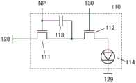
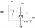
电路11可以包括晶体管101、晶体管102及电容器104。晶体管101的源极和漏极中的一个与电容器104的一个电极电连接。电容器104的另一个电极与晶体管102的源极和漏极中的一个电连接。
电路10可以包括晶体管103及电路区块110。电路区块110可以包括晶体管、电容器及显示元件等。晶体管103的源极和漏极中的一个与晶体管101的源极和漏极中的一个电连接。晶体管103的源极和漏极中的另一个与电路区块110电连接。
在此,将使晶体管101的源极和漏极中的一个、电容器104的一个电极及晶体管103的源极和漏极中的一个连接的布线称为节点NM。另外,将使晶体管103的源极和漏极中的另一个与电路区块110连接的布线称为节点NP。节点NP可以处于浮动状态,电路区块110所包括的显示元件根据节点NP的电位工作。Here, a wiring connecting one of the source and drain of the
对电路10及电路11所包括的构成要素与各种布线的连接进行说明。晶体管101的栅极与布线121电连接。晶体管102的栅极与布线122电连接。晶体管103的栅极与布线123电连接。晶体管101的源极和漏极中的另一个与布线125电连接。晶体管102的源极和漏极中的另一个与布线126电连接。The connection between the components included in the
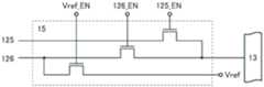
布线121、122、123(123[1]至[n])被用作栅极线。例如,布线121、122与栅极驱动器14a电连接。布线123与栅极驱动器14b电连接。布线125、126被用作源极线并通过电路15与源极驱动器13电连接(参照图1)。The
电路15例如可以具有图3所示的结构。电路15可以被用作选择电路并将从源极驱动器13输入的电位输出到布线125或布线126。另外,可以将电位“Vref”(例如,0V等基准电位)输出到布线126。通过由信号Vref_EN、125_EN及126_EN控制与各布线连接的晶体管,可以控制各电位的输出。注意,有时不设置电路15。The
在电路11中,首先向节点NM写入第一数据(权重:W)。此时,向电容器104的另一个电极供应“Vref”,在电容器104中保持“W-Vref”。接着,使节点NM为浮动状态,向电容器104的另一个电极供应第二数据(数据:D),由于电容耦合而节点NM的电位为“W-Vref+D”。In the
在此,若满足“W”=“D”、“Vref”=0V且节点NM的电容充分小,则节点NM的电位为“2D”或“2W”,而可以将源极驱动器13的输出的两倍左右的电位输出到节点NM。因此,即便使用通用驱动器IC,也可以用于需要高电压的用途(例如,在控制灰度时需要高电压的液晶元件等)。另外,可以将用来驱动一般的液晶元件及发光元件等的从源极驱动器13供应的电压减少至1/2左右,由此可以使显示装置低功耗化。Here, if “W”=“D”, “Vref ”=0V and the capacitance of the node NM is sufficiently small, the potential of the node NM is “2D” or “2W”, and the output of the
作为第一数据(权重:W),也可以供应校正数据。例如,通过将亮度校正数据加上图像数据,可以校正显示装置特有的亮度的偏差。此外,由于能够按每个像素校正亮度,所以可以将其用于HDR显示。另外,在作为显示元件使用发光元件的情况下,显示质量受到驱动晶体管的阈值电压偏差的影响,因此也可以将该晶体管的阈值电压校正数据作为第一数据(权重:W)供应来改善显示质量。注意,第一数据(权重:W)与第二数据(数据:D)也可以互相调换。As the first data (weight: W), correction data may also be supplied. For example, by adding the luminance correction data to the image data, it is possible to correct the variation in luminance specific to the display device. In addition, since brightness can be corrected on a per-pixel basis, it can be used for HDR display. In addition, when a light-emitting element is used as a display element, since the display quality is affected by the variation of the threshold voltage of the driving transistor, the threshold voltage correction data of the transistor can be supplied as the first data (weight: W) to improve the display quality. . Note that the first data (weight: W) and the second data (data: D) may be exchanged with each other.
在本发明的一个方式中,根据上述电位的加法工作使特定电路10的晶体管103导通,并且确定节点NP的电位(=节点NM的电位)。通过依次对电路10[1]至电路10[n]进行这种工作,可以确定各电路10的节点NP的电位。就是说,可以向各像素供应不同的图像数据。In one embodiment of the present invention, the
节点NM、节点NP被用作存储节点。通过使连接于各节点的晶体管导通,可以将数据写入到各节点。此外,通过使该晶体管非导通,可以将该数据保持在各节点中。通过作为该晶体管使用关态电流极低的晶体管可以抑制泄漏电流,由此能够长时间保持各节点的电位。该晶体管例如可以使用在沟道形成区域中包含金属氧化物的晶体管(以下,OS晶体管)。Node NM, Node NP are used as storage nodes. Data can be written to each node by turning on the transistor connected to each node. Also, by making the transistor non-conductive, the data can be held in each node. By using a transistor with an extremely low off-state current as the transistor, leakage current can be suppressed, and the potential of each node can be maintained for a long time. As the transistor, for example, a transistor containing a metal oxide in a channel formation region (hereinafter, an OS transistor) can be used.
具体而言,作为晶体管101、102、103,优选使用OS晶体管。此外,可以将OS晶体管用于电路区块110所包括的构成要素。另外,当在泄漏电流量为可允许范围内进行工作时,可以使用沟道形成区域中包含Si的晶体管(以下,Si晶体管)。此外,可以组合使用OS晶体管及Si晶体管。作为上述Si晶体管,可以举出含有非晶硅的晶体管、含有结晶硅(典型的有低温多晶硅、单晶硅)的晶体管等。Specifically, as the
作为用于OS晶体管的半导体材料,可以使用能隙为2eV以上,优选为2.5eV以上,更优选为3eV以上的金属氧化物。典型地有含有铟的氧化物半导体等,例如,可以使用后面提到的CAAC-OS或CAC-OS等。CAAC-OS中构成结晶的原子稳定,适用于重视可靠性的晶体管等。CAC-OS呈现高迁移率特性,适用于进行高速驱动的晶体管等。As a semiconductor material for an OS transistor, a metal oxide having an energy gap of 2 eV or more, preferably 2.5 eV or more, and more preferably 3 eV or more can be used. Typically, there are oxide semiconductors containing indium and the like, and for example, CAAC-OS or CAC-OS mentioned later can be used. The atoms constituting crystals in CAAC-OS are stable, and are suitable for transistors where reliability is important. CAC-OS exhibits high mobility characteristics and is suitable for high-speed driving of transistors and the like.
由于OS晶体管的半导体层具有大能隙,所以呈现极低的关态电流特性,仅为几yA/μm(每沟道宽度1μm的电流值)。与Si晶体管不同,OS晶体管具有不会发生碰撞电离、雪崩击穿、短沟道效应等的特性,因此能够形成高可靠性的电路。此外,Si晶体管所引起的起因于结晶性的不均匀的电特性偏差不容易产生在OS晶体管中。Since the semiconductor layer of the OS transistor has a large energy gap, it exhibits extremely low off-state current characteristics of only a few μA/μm (current value per channel width of 1 μm). Unlike Si transistors, OS transistors have characteristics that do not cause impact ionization, avalanche breakdown, short-channel effects, and the like, and thus can form highly reliable circuits. In addition, variation in electrical characteristics due to nonuniform crystallinity caused by Si transistors is unlikely to occur in OS transistors.
作为OS晶体管中的半导体层,例如可以采用包含铟、锌及M(铝、钛、镓、锗、钇、锆、镧、铈、锡、钕或铪等金属)的以“In-M-Zn类氧化物”表示的膜。As the semiconductor layer in the OS transistor, for example, a compound called "In-M-Zn" containing indium, zinc, and M (a metal such as aluminum, titanium, gallium, germanium, yttrium, zirconium, lanthanum, cerium, tin, neodymium, or hafnium) can be used. Oxide-like" films.
当构成半导体层的氧化物半导体为In-M-Zn类氧化物时,优选用来形成In-M-Zn氧化物膜的溅射靶材的金属元素的原子数比满足In≥M及Zn≥M。这种溅射靶材的金属元素的原子数比优选为In:M:Zn=1:1:1、In:M:Zn=1:1:1.2、In:M:Zn=3:1:2、In:M:Zn=4:2:3、In:M:Zn=4:2:4.1、In:M:Zn=5:1:6、In:M:Zn=5:1:7、In:M:Zn=5:1:8等。注意,所形成的半导体层的原子数比分别有可能在上述溅射靶材中的金属元素的原子数比的±40%的范围内变动。When the oxide semiconductor constituting the semiconductor layer is an In-M-Zn-based oxide, it is preferable that the atomic ratio of the metal element of the sputtering target for forming the In-M-Zn oxide film satisfies In≧M and Zn≧ M. The atomic ratio of the metal elements in the sputtering target is preferably In:M:Zn=1:1:1, In:M:Zn=1:1:1.2, In:M:Zn=3:1:2 , In:M:Zn=4:2:3, In:M:Zn=4:2:4.1, In:M:Zn=5:1:6, In:M:Zn=5:1:7, In : M:Zn=5:1:8, etc. Note that the atomic ratio of the formed semiconductor layer may vary within a range of ±40% of the atomic ratio of the metal element in the above-described sputtering target, respectively.
作为半导体层,使用载流子密度低的氧化物半导体。例如,作为半导体层可以使用载流子密度为1×10¹⁷/cm3以下,优选为1×1015/cm3以下,更优选为1×1013/cm3以下,进一步优选为1×1011/cm3以下,更进一步优选为小于1×1010/cm3且为1×10-9/cm3以上的氧化物半导体。将这样的氧化物半导体称为高纯度本征或实质上高纯度本征的氧化物半导体。该氧化物半导体的缺陷态密度低,因此可以说是具有稳定的特性的氧化物半导体。As the semiconductor layer, an oxide semiconductor having a low carrier density is used. For example, the carrier density that can be used as the semiconductor layer is 1×10¹⁷ /cm3 or less, preferably 1×10¹⁵ /cm3 or less, more preferably 1×10¹³ /cm3 or less, and still more preferably 1×10¹¹ /cm3 or less, more preferably less than 1 × 10¹⁰ /cm3 and 1 × 10⁻⁹ /cm3 or more of an oxide semiconductor. Such an oxide semiconductor is called a high-purity intrinsic or substantially high-purity intrinsic oxide semiconductor. Since this oxide semiconductor has a low density of defect states, it can be said that it is an oxide semiconductor having stable characteristics.
注意,本发明不局限于上述记载,可以根据所需的晶体管的半导体特性及电特性(场效应迁移率、阈值电压等)来使用具有适当的组成的材料。另外,优选适当地设定半导体层的载流子密度、杂质浓度、缺陷密度、金属元素与氧的原子数比、原子间距离、密度等,以得到所需的晶体管的半导体特性。Note that the present invention is not limited to the above description, and a material having an appropriate composition may be used in accordance with desired semiconductor characteristics and electrical characteristics (field-effect mobility, threshold voltage, etc.) of the transistor. In addition, the carrier density, impurity concentration, defect density, atomic ratio of metal element to oxygen, interatomic distance, density, etc. of the semiconductor layer are preferably appropriately set to obtain desired semiconductor characteristics of the transistor.
当构成半导体层的氧化物半导体包含第14族元素之一的硅或碳时,氧空位增加,会使该半导体层变为n型。因此,将半导体层中的硅或碳的浓度(通过二次离子质谱分析法测得的浓度)设定为2×10¹⁸atoms/cm3以下,优选为2×1017atoms/cm3以下。When the oxide semiconductor constituting the semiconductor layer contains silicon or carbon, which is one of the Group 14 elements, oxygen vacancies increase, and the semiconductor layer becomes n-type. Therefore, the concentration of silicon or carbon in the semiconductor layer (concentration measured by secondary ion mass spectrometry) is set to 2×10¹⁸ atoms/cm3 or less, preferably 2×10¹⁷ atoms/cm3 or less.
另外,有时当碱金属及碱土金属与氧化物半导体键合时生成载流子,而使晶体管的关态电流增大。因此,将半导体层中的碱金属或碱土金属的浓度(通过二次离子质谱分析法测得的浓度)设定为1×10¹⁸atoms/cm3以下,优选为2×1016atoms/cm3以下。In addition, when an alkali metal and an alkaline earth metal are bonded to an oxide semiconductor, a carrier may be generated, and the off-state current of the transistor may increase. Therefore, the concentration of the alkali metal or alkaline earth metal in the semiconductor layer (concentration measured by secondary ion mass spectrometry) is set to 1×10¹⁸ atoms/cm3 or less, preferably 2×10¹⁶ atoms/cm3 the following.
另外,当构成半导体层的氧化物半导体含有氮时生成作为载流子的电子,载流子密度增加而容易变为n型。其结果是,使用含有氮的氧化物半导体的晶体管容易变为常开启特性。因此,半导体层中的氮浓度(通过二次离子质谱分析法测得的浓度)优选为5×10¹⁸atoms/cm3以下。In addition, when the oxide semiconductor constituting the semiconductor layer contains nitrogen, electrons are generated as carriers, and the carrier density increases, and it becomes easy to become n-type. As a result, a transistor using an oxide semiconductor containing nitrogen tends to have normally-on characteristics. Therefore, the nitrogen concentration (concentration measured by secondary ion mass spectrometry) in the semiconductor layer is preferably 5×10¹⁸ atoms/cm3 or less.
另外,当构成半导体层的氧化物半导体包含氢时,氢与键合于金属原子的氧起反应生成水,因此有时在氧化物半导体中形成氧空位。在氧化物半导体中的沟道形成区域包含氧空位的情况下,晶体管趋于具有常开启特性。再者,有时氢进入氧空位中的缺陷被用作供体而生成作为载流子的电子。此外,有时由于氢的一部分与键合于金属原子的氧键合,生成作为载流子的电子。因此,使用包含较多的氢的氧化物半导体的晶体管容易具有常开启特性。In addition, when the oxide semiconductor constituting the semiconductor layer contains hydrogen, the hydrogen reacts with oxygen bonded to the metal atom to generate water, so that oxygen vacancies may be formed in the oxide semiconductor. In the case where the channel formation region in the oxide semiconductor contains oxygen vacancies, the transistor tends to have normally-on characteristics. Furthermore, a defect in which hydrogen enters an oxygen vacancy is sometimes used as a donor to generate electrons as carriers. In addition, electrons serving as carriers may be generated due to the bonding of a part of hydrogen to oxygen bonded to metal atoms. Therefore, a transistor using an oxide semiconductor containing a large amount of hydrogen tends to have normally-on characteristics.
氢进入到氧空位中的缺陷会被用作氧化物半导体的供体。然而,难以对该缺陷定量地进行评价。因此,在氧化物半导体中,有时不是根据供体浓度而是根据载流子浓度进行评价。由此,在本说明书等中,有时作为氧化物半导体的参数,不采用供体浓度而采用假定为不被施加电场的状态的载流子浓度。就是说,有时也可以将本说明书等所记载的“载流子浓度”称为“供体浓度”。Defects in which hydrogen enters oxygen vacancies are used as donors for oxide semiconductors. However, it is difficult to quantitatively evaluate this defect. Therefore, in oxide semiconductors, evaluation is sometimes performed not based on the concentration of the donor but based on the concentration of the carrier. Therefore, in this specification and the like, as a parameter of the oxide semiconductor, a carrier concentration assumed to be in a state in which an electric field is not applied may be adopted instead of the donor concentration. That is, the "carrier concentration" described in this specification and the like may be referred to as "donor concentration" in some cases.
由此,优选尽可能减少氧化物半导体中的氢。具体而言,在氧化物半导体中,利用二次离子质谱分析法(SIMS:Secondary Ion Mass Spectrometry)测得的氢浓度低于1×10²⁰atoms/cm3,优选低于1×1019atoms/cm3,更优选低于5×1018atoms/cm3,进一步优选低于1×1018atoms/cm3。通过将氢等杂质被充分减少的氧化物半导体用于晶体管的沟道形成区域,可以赋予稳定的电特性。Therefore, it is preferable to reduce hydrogen in the oxide semiconductor as much as possible. Specifically, in the oxide semiconductor, the hydrogen concentration measured by Secondary Ion Mass Spectrometry (SIMS: Secondary Ion Mass Spectrometry) is lower than 1×10²⁰ atoms/cm3 , preferably lower than 1×10¹⁹ atoms/cm cm3 , more preferably less than 5×10¹⁸ atoms/cm3 , still more preferably less than 1×10¹⁸ atoms/cm3 . Stable electrical characteristics can be imparted by using an oxide semiconductor in which impurities such as hydrogen are sufficiently reduced for the channel formation region of the transistor.
另外,半导体层例如也可以具有非单晶结构。非单晶结构例如包括具有c轴取向的结晶的CAAC-OS(C-Axis Aligned Crystalline Oxide Semiconductor)、多晶结构、微晶结构或非晶结构。在非单晶结构中,非晶结构的缺陷态密度最高,而CAAC-OS的缺陷态密度最低。In addition, the semiconductor layer may have, for example, a non-single crystal structure. The non-single crystal structure includes, for example, a crystalline CAAC-OS (C-Axis Aligned Crystalline Oxide Semiconductor) having a c-axis orientation, a polycrystalline structure, a microcrystalline structure, or an amorphous structure. Among the non-single-crystal structures, the amorphous structure has the highest density of defect states, while that of CAAC-OS is the lowest.
非晶结构的氧化物半导体膜例如具有无秩序的原子排列且不具有结晶成分。或者,非晶结构的氧化物膜例如是完全的非晶结构且不具有结晶部。An oxide semiconductor film of an amorphous structure has, for example, a disordered atomic arrangement and no crystalline component. Alternatively, the oxide film of the amorphous structure has, for example, a completely amorphous structure and does not have a crystal part.
此外,半导体层也可以为具有非晶结构的区域、微晶结构的区域、多晶结构的区域、CAAC-OS的区域和单晶结构的区域中的两种以上的混合膜。混合膜有时例如具有包括上述区域中的两种以上的区域的单层结构或叠层结构。In addition, the semiconductor layer may be a mixed film of two or more of an amorphous structure region, a microcrystalline structure region, a polycrystalline structure region, a CAAC-OS region, and a single crystal structure region. The hybrid film may have, for example, a single-layer structure or a stacked-layer structure including two or more of the above-mentioned regions.
以下对非单晶半导体层的一个方式的CAC(Cloud-Aligned Composite)-OS的构成进行说明。The configuration of CAC (Cloud-Aligned Composite)-OS, which is one form of the non-single crystal semiconductor layer, will be described below.
CAC-OS例如是指包含在氧化物半导体中的元素不均匀地分布的构成,其中包含不均匀地分布的元素的材料的尺寸为0.5nm以上且10nm以下,优选为1nm以上且2nm以下或近似的尺寸。注意,在下面也将在氧化物半导体中一个或多个金属元素不均匀地分布且包含该金属元素的区域以0.5nm以上且10nm以下,优选为1nm以上且2nm以下或近似的尺寸混合的状态称为马赛克(mosaic)状或补丁(patch)状。CAC-OS, for example, refers to a structure in which elements contained in an oxide semiconductor are unevenly distributed, and the size of the material containing the unevenly distributed elements is 0.5 nm or more and 10 nm or less, preferably 1 nm or more and 2 nm or less, or approximately size of. Note that in the following, one or more metal elements are unevenly distributed in the oxide semiconductor and regions containing the metal elements are mixed in a size of 0.5 nm or more and 10 nm or less, preferably 1 nm or more and 2 nm or less, or similar. Known as mosaic (mosaic) shape or patch (patch) shape.
氧化物半导体优选至少包含铟。尤其是,优选包含铟及锌。除此之外,也可以还包含选自铝、镓、钇、铜、钒、铍、硼、硅、钛、铁、镍、锗、锆、钼、镧、铈、钕、铪、钽、钨和镁等中的一种或多种。The oxide semiconductor preferably contains at least indium. In particular, indium and zinc are preferably contained. In addition, it can also contain aluminum, gallium, yttrium, copper, vanadium, beryllium, boron, silicon, titanium, iron, nickel, germanium, zirconium, molybdenum, lanthanum, cerium, neodymium, hafnium, tantalum, tungsten and one or more of magnesium, etc.
例如,In-Ga-Zn氧化物中的CAC-OS(在CAC-OS中,尤其可以将In-Ga-Zn氧化物称为CAC-IGZO)是指材料分成铟氧化物(以下,称为InOX1(X1为大于0的实数))或铟锌氧化物(以下,称为InX2ZnY2OZ2(X2、Y2及Z2为大于0的实数))以及镓氧化物(以下,称为GaOX3(X3为大于0的实数))或镓锌氧化物(以下,称为GaX4ZnY4OZ4(X4、Y4及Z4为大于0的实数))等而成为马赛克状,且马赛克状的InOX1或InX2ZnY2OZ2均匀地分布在膜中的构成(以下,也称为云状)。For example, CAC-OS in In-Ga-Zn oxide (in CAC-OS, In-Ga-Zn oxide can especially be referred to as CAC-IGZO) means that the material is divided into indium oxide (hereinafter, referred to as InOX1 (X1 is a real number greater than 0)) or indium zinc oxide (hereinafter referred to as InX2 ZnY2 OZ2 (X2, Y2 and Z2 are real numbers greater than 0)) and gallium oxide (hereinafter referred to as GaOX3 (X3 is a real number greater than 0)) or gallium zinc oxide (hereinafter, referred to as GaX4 ZnY4 OZ4 (X4, Y4 and Z4 are real numbers greater than 0)), etc. to form a mosaic, and mosaic-like InOX1 Or a structure in which InX2 ZnY2 OZ2 is uniformly distributed in the film (hereinafter, also referred to as cloud shape).
换言之,CAC-OS是具有以GaOX3为主要成分的区域和以InX2ZnY2OZ2或InOX1为主要成分的区域混在一起的构成的复合氧化物半导体。在本说明书中,例如,当第一区域的In与元素M的原子数比大于第二区域的In与元素M的原子数比时,第一区域的In浓度高于第二区域。In other words, CAC-OS is a composite oxide semiconductor having a structure in which a region mainly composed of GaOX3 and a region mainly composed of InX2 ZnY2 OZ2 or InOX1 are mixed together. In this specification, for example, when the atomic ratio of In to the element M of the first region is larger than the atomic ratio of In to the element M of the second region, the In concentration of the first region is higher than that of the second region.
注意,IGZO是通称,有时是指包含In、Ga、Zn及O的化合物。作为典型例子,可以举出以InGaO3(ZnO)m1(m1为自然数)或In(1+x0)Ga(1-x0)O3(ZnO)m0(-1≤x0≤1,m0为任意数)表示的结晶性化合物。Note that IGZO is a generic term and may refer to a compound containing In, Ga, Zn, and O. Typical examples include InGaO3 (ZnO)m1 (m1 is a natural number) or In(1+x0) Ga(1-x0) O3 (ZnO)m0 (-1≤x0≤1, where m0 is an arbitrary number ) represents a crystalline compound.
上述结晶性化合物具有单晶结构、多晶结构或CAAC结构。CAAC结构是多个IGZO的纳米晶具有c轴取向性且在a-b面上以不取向的方式连接的结晶结构。The above-mentioned crystalline compound has a single crystal structure, a polycrystalline structure or a CAAC structure. The CAAC structure is a crystalline structure in which a plurality of IGZO nanocrystals have c-axis orientation and are connected in a non-oriented manner on the a-b planes.
另一方面,CAC-OS与氧化物半导体的材料构成有关。CAC-OS是指如下构成:在包含In、Ga、Zn及O的材料构成中,一部分中观察到以Ga为主要成分的纳米粒子状区域以及一部分中观察到以In为主要成分的纳米粒子状区域分别以马赛克状无规律地分散。因此,在CAC-OS中,结晶结构是次要因素。On the other hand, CAC-OS is related to the material composition of oxide semiconductors. CAC-OS refers to a structure in which, in a material structure including In, Ga, Zn, and O, a nanoparticle-like region mainly composed of Ga is observed in a part and a nanoparticle-shaped region mainly composed of In is observed in a part. The regions are scattered irregularly in a mosaic shape, respectively. Therefore, in CAC-OS, the crystalline structure is a secondary factor.
CAC-OS不包含组成不同的两种以上的膜的叠层结构。例如,不包含由以In为主要成分的膜与以Ga为主要成分的膜的两层构成的结构。CAC-OS does not include a stacked structure of two or more films with different compositions. For example, a structure composed of two layers of a film containing In as a main component and a film containing Ga as a main component is not included.
注意,有时观察不到以GaOX3为主要成分的区域与以InX2ZnY2OZ2或InOX1为主要成分的区域之间的明确的边界。Note that a clear boundary between the region mainly composed of GaOX3 and the region mainly composed of InX2 ZnY2 OZ2 or InOX1 may not be observed.
在CAC-OS中包含选自铝、钇、铜、钒、铍、硼、硅、钛、铁、镍、锗、锆、钼、镧、铈、钕、铪、钽、钨和镁等中的一种或多种以代替镓的情况下,CAC-OS是指如下构成:一部分中观察到以该金属元素为主要成分的纳米粒子状区域以及一部分中观察到以In为主要成分的纳米粒子状区域以马赛克状无规律地分散。In the CAC-OS, a compound selected from the group consisting of aluminum, yttrium, copper, vanadium, beryllium, boron, silicon, titanium, iron, nickel, germanium, zirconium, molybdenum, lanthanum, cerium, neodymium, hafnium, tantalum, tungsten and magnesium is included. In the case where one or more of gallium are replaced, CAC-OS refers to a structure in which a nanoparticulate region mainly composed of the metal element is observed in a part, and a nanoparticulate region mainly composed of In is observed in a part. Areas are scattered irregularly in a mosaic.
CAC-OS例如可以通过在对衬底不进行意图性的加热的条件下利用溅射法来形成。在利用溅射法形成CAC-OS的情况下,作为成膜气体,可以使用选自惰性气体(典型的是氩)、氧气体和氮气体中的一种或多种。另外,成膜时的成膜气体的总流量中的氧气体的流量比越低越好,例如,将氧气体的流量比设定为0%以上且低于30%,优选为0%以上且10%以下。CAC-OS can be formed by sputtering, for example, without intentionally heating the substrate. In the case of forming the CAC-OS by the sputtering method, as the film-forming gas, one or more kinds selected from an inert gas (typically argon), an oxygen gas, and a nitrogen gas can be used. In addition, the lower the flow rate ratio of the oxygen gas in the total flow rate of the film formation gas at the time of film formation, the better. For example, the flow rate ratio of the oxygen gas is set to 0% or more and less than 30%, preferably 0% or more and 10% or less.
CAC-OS具有如下特征:通过根据X射线衍射(XRD:X-ray diffraction)测定法之一的Out-of-plane法利用θ/2θ扫描进行测定时,观察不到明确的峰值。也就是说,根据X射线衍射测定,可知在测定区域中没有a-b面方向及c轴方向上的取向。CAC-OS is characterized in that no clear peak is observed when measured by θ/2θ scanning by the Out-of-plane method, which is one of X-ray diffraction (XRD: X-ray diffraction) measurement methods. That is, according to the X-ray diffraction measurement, it was found that there was no orientation in the a-b plane direction and the c-axis direction in the measurement region.
另外,在通过照射束径为1nm的电子束(也称为纳米束)而取得的CAC-OS的电子衍射图案中,观察到环状的亮度高的区域(环状区域)以及在该环状区域内的多个亮点。由此,根据电子衍射图案,可知CAC-OS的结晶结构具有在平面方向及截面方向上没有取向的nc(nano-crystal)结构。In addition, in the electron diffraction pattern of CAC-OS obtained by irradiating an electron beam (also referred to as a nanobeam) with a beam diameter of 1 nm, a ring-shaped high-brightness region (ring-shaped region) and a ring-shaped region with high brightness were observed. Multiple bright spots in the area. As a result, from the electron diffraction pattern, it was found that the crystal structure of CAC-OS has an nc (nano-crystal) structure that is not oriented in the plane direction and the cross-sectional direction.
另外,例如在In-Ga-Zn氧化物的CAC-OS中,根据通过能量分散型X射线分析法(EDX:Energy Dispersive X-ray spectroscopy)取得的EDX面分析(mapping)图像,可确认到:具有以GaOX3为主要成分的区域及以InX2ZnY2OZ2或InOX1为主要成分的区域不均匀地分布而混合的构成。In addition, for example, in the CAC-OS of In-Ga-Zn oxide, from the EDX surface analysis (mapping) image obtained by energy dispersive X-ray spectroscopy (EDX: Energy Dispersive X-ray spectroscopy), it can be confirmed that: It has a structure in which a region containing GaOX3 as a main component and a region containing InX2 ZnY2 OZ2 or InOX1 as a main component are unevenly distributed and mixed.
CAC-OS的结构与金属元素均匀地分布的IGZO化合物不同,具有与IGZO化合物不同的性质。换言之,CAC-OS具有以GaOX3等为主要成分的区域及以InX2ZnY2OZ2或InOX1为主要成分的区域互相分离且以各元素为主要成分的区域为马赛克状的构成。The structure of CAC-OS is different from that of IGZO compounds in which metal elements are uniformly distributed, and has properties different from those of IGZO compounds. In other words, the CAC-OS has a mosaic-like structure in which the region mainly composed of GaOX3 and the like and the region mainly composed of InX2 ZnY2 OZ2 or InOX1 are separated from each other and the region mainly composed of each element is formed.
在此,以InX2ZnY2OZ2或InOX1为主要成分的区域的导电性高于以GaOX3等为主要成分的区域。换言之,当载流子流过以InX2ZnY2OZ2或InOX1为主要成分的区域时,呈现氧化物半导体的导电性。因此,当以InX2ZnY2OZ2或InOX1为主要成分的区域在氧化物半导体中以云状分布时,可以实现高场效应迁移率(μ)。Here, the conductivity of the region mainly composed of InX2 ZnY2 OZ2 or InOX1 is higher than that of the region mainly composed of GaOX3 or the like. In other words, when carriers flow through the region mainly composed of InX2 ZnY2 OZ2 or InOX1 , the conductivity of an oxide semiconductor is exhibited. Therefore, when a region mainly composed of InX2 ZnY2 OZ2 or InOX1 is distributed in a cloud shape in the oxide semiconductor, high field-effect mobility (μ) can be achieved.
另一方面,以GaOX3等为主要成分的区域的绝缘性高于以InX2ZnY2OZ2或InOX1为主要成分的区域。换言之,当以GaOX3等为主要成分的区域在氧化物半导体中分布时,可以抑制泄漏电流而实现良好的开关工作。On the other hand, the insulating property of the region mainly composed of GaOX3 or the like is higher than that of the region mainly composed of InX2 ZnY2 OZ2 or InOX1 . In other words, when a region mainly composed of GaOX3 or the like is distributed in the oxide semiconductor, leakage current can be suppressed and a good switching operation can be realized.
因此,当将CAC-OS用于半导体元件时,通过起因于GaOX3等的绝缘性及起因于InX2ZnY2OZ2或InOX1的导电性的互补作用可以实现高通态电流(Ion)及高场效应迁移率(μ)。Therefore ,whenCAC -OS isused for a semiconductor element, highon -state current (Ion) and High field effect mobility (μ).
另外,使用CAC-OS的半导体元件具有高可靠性。因此,CAC-OS适用于各种半导体装置的构成材料。In addition, semiconductor elements using CAC-OS have high reliability. Therefore, CAC-OS is suitable for constituent materials of various semiconductor devices.
注意,图2示出将电路11配置在像素20[1]中的结构,但是也可以配置在其他像素中。此外,如图4所示,也可以将电路11的构成要素分散地配置在多个区域中。Note that FIG. 2 shows a configuration in which the
例如,可以在像素20[1]中配置晶体管101,在像素20[2]中配置晶体管102,在像素20[n-1]及像素20[n]中配置被分割的电容器104。如此,通过分散地配置电路11的构成要素,可以减少设置在各像素中的晶体管及电容器等构成要素的个数及占有面积,由此可以提高开口率。For example, the
注意,虽然在图4中未图示,但是也可以有不配置电路11的构成要素的像素。另外,也可以在一个像素中配置有多个该构成要素。此外,电容器也可以不被分割地配置在一个像素中。此外,也可以增加电容器被分割成的个数并将其分割配置在三个以上的像素中。Note that, although not shown in FIG. 4 , there may be pixels in which the constituent elements of the
接着,参照图5所示的时序图说明图2或图4所示的像素区块12的工作方法。注意,在以下的说明中,高电位记作“H”,低电位记作“L”。此外,向像素20[1]供应的权重记作“W[1]”,图像数据记作“D[1]”,向像素20[2]供应的权重记作“W[2]”,图像数据记作“D[2]”,向像素20[n-1]供应的权重记作“W[n-1]”,图像数据记作“D[n-1]”,向像素20[n]供应的权重记作“W[n]”,图像数据记作“D[n]”。作为“Vref”,例如可以使用0V、GND电位或特定的基准电位。Next, an operation method of the
注意,这里在电位的分布、耦合或损耗中不考虑因电路的结构、工作时机等引起的详细变化。由使用电容器的电容耦合引起的电位变化依赖于电容器和与该电容器连接的负载的容量比,但是为了便于说明,假设电路区块110的电容值为足够小的值。Note that detailed changes due to the structure of the circuit, the timing of operation, and the like are not considered here in the distribution, coupling, or loss of the potential. The potential change caused by the capacitive coupling using the capacitor depends on the capacity ratio of the capacitor and the load connected to the capacitor, but for convenience of explanation, the capacitance value of the
首先,说明像素20[1]中的“W[1]”的写入工作。First, the writing operation of "W[1]" in the pixel 20[1] will be described.
在时刻T1,向布线125供应“W[1]”,向布线126供应”Vref”,使布线121、122、123[1]的电位为“H”,由此,晶体管102导通,电容器104的另一个电极的电位为“Vref”。该工作是用来进行后面的加法工作(电容耦合工作)的复位工作。At time T1, "W[1]" is supplied to the
另外,晶体管101、103导通,布线125的电位被写入到节点NP[1]。该工作是权重的写入工作,节点NP[1]的电位为“W[1]”。In addition, the
在时刻T2,使布线121、122的电位为“L”,使布线123[1]的电位为“H”,由此,晶体管101、102非导通。此时,节点NP[1]保持“W[1]”。此外,电容器104保持“W[1]-Vref”。到此为止是像素20[1]中的“W[1]”的写入工作。At time T2, the potential of the
接着,说明像素20[1]中的“D[1]”的加法工作。Next, the addition operation of "D[1]" in the pixel 20[1] will be described.
在时刻T3,向布线126供应“D[1]”,使布线121的电位为“L”,使布线122、123[1]的电位为“H”,由此,晶体管102、103导通。此时,电容器104的另一个电极的电位为“D[1]”,由于电容耦合而“D[1]”被附加到节点NP[1]的电位。该工作是加法工作,节点NP[1]的电位为“W[1]-Vref+D[1]”。此时,若“Vref”=0,则节点NP[1]的电位为“W[1]+D[1]”。节点NP[1]的电位被供应到显示元件而进行显示。At time T3, "D[1]" is supplied to the
在时刻T4,当布线121、122、123[1]的电位为“L”时,晶体管103非导通,节点NP[1]的电位被保持,直到下一帧的工作为止继续显示。以上是像素20[1]的工作说明。At time T4, when the potentials of the
接着,说明像素20[2]中的“W[2]”的写入工作。Next, the writing operation of "W[2]" in the pixel 20[2] will be described.
在时刻T5,向布线125供应“W[2]”,向布线126供应”Vref”,布线121、122、123[2]的电位为“H”,由此,晶体管102导通,电容器104的另一个电极的电位为“Vref”。At time T5, “W[2]” is supplied to the
另外,晶体管101、103导通,布线125的电位被写入到节点NP[2]。该工作是权重的写入工作,节点NP[2]的电位为“W[2]”。In addition, the
在时刻T6,使布线121、122的电位为“L”,使布线123[2]的电位为“H”,由此,晶体管101,102非导通。此时,节点NP[2]保持“W[2]”。另外,电容器104保持“W[2]-Vref”。到此为止是像素20[2]中的“W[2]”的写入工作。At time T6, the potential of the
接着,说明像素20[2]中的“D[2]”的加法工作。Next, the addition operation of "D[2]" in the pixel 20[2] will be described.
在时刻T7,向布线126供应“D[2]”,使布线121的电位为“L”,使布线122、123[1]的电位为“H”,由此,晶体管102、103导通。此时,电容器104的另一个电极的电位为“D[2]”,由于电容耦合而“D[2]”被附加到节点NP[1]的电位。该工作是加法工作,节点NP[1]的电位为“W[2]-Vref+D[2]”。此时,若“Vref”=0,则节点NP[2]的电位为“W[2]+D[2]”。节点NP[2]的电位被供应到显示元件而进行显示。At time T7, "D[2]" is supplied to the
在时刻T8,当布线121、122、123[2]的电位为“L”时,晶体管103非导通,节点NP[2]的电位被保持,直到下一帧的工作为止继续显示。以上是像素20[2]的工作说明。At time T8, when the potentials of the
节点NP[2]的电位被供应到显示元件而进行显示。以上是像素20[2]的工作说明。通过在时刻T9至T12使像素20[n-1]进行同样的工作,可以在像素20[n-1]中进行对应“W[n-1]+D[n-1]”的显示。此外,通过在时刻T13至T16使像素20[n]进行同样的工作,可以在像素20[n]中进行对应“W[n]+D[n]”的显示。The potential of the node NP[2] is supplied to the display element for display. The above is the working description of pixel 20 [2]. By causing the pixel 20[n-1] to perform the same operation at times T9 to T12, display corresponding to "W[n-1]+D[n-1]" can be performed in the pixel 20[n-1]. Further, by causing the pixel 20[n] to perform the same operation at the times T13 to T16, the display corresponding to "W[n]+D[n]" can be performed in the pixel 20[n].
通过上述方式,可以使像素区块12工作。In the above manner, the
电路11也可以具有图6A所示的结构。图6A所示的电路11与图2或图4所示的电路11的不同之处在于包括晶体管105及一个源极线。The
晶体管105的栅极与布线122电连接。晶体管105的源极和漏极中的一个与电容器104的另一个电极电连接。晶体管105的源极和漏极中的另一个与能够供应“Vref”的布线电连接。晶体管101的源极和漏极中的另一个及晶体管102的源极和漏极中的另一个与布线125电连接。The gate of the
在图2或图4所示的电路11的结构中,从布线126切换地供应数据(D)和“Vref”,在图6A所示的电路11的结构中,通过专用路径供应“Vref”,因此可以从布线125切换地供应权重(W)和数据(D)。因此,可以减少源极线中的一个。In the structure of the
参照图7所示的时序图说明在图2或图4所示的像素区块12中使用图6A所示的电路11时的工作。The operation when the
在时刻T1,向布线125供应“W[1]”,使布线121、123[1]的电位为“H”,由此,晶体管105导通,电容器104的另一个电极的电位为“Vref”。该工作是用来进行后面的加法工作(电容耦合工作)的复位工作。At time T1, "W[1]" is supplied to the
另外,晶体管101、103导通,布线125的电位被写入到节点NP[1]。该工作是权重的写入工作,节点NP[1]的电位为“W[1]”。In addition, the
在时刻T2,使布线121的电位为“L”,布线123[1]的电位为“H”,晶体管101、105非导通。此时,节点NP[1]保持“W[1]”。此外,电容器104保持“W[1]-Vref”。到此为止是像素20[1]中的“W[1]”的写入工作。At time T2, the potential of the
在时刻T3,向布线125供应“D[1]”,使布线121的电位为“L”,使布线122、123[1]的电位为“H”,由此,晶体管102、103导通。此时,电容器104的另一个电极的电位为“D[1]”,由于电容耦合而“D[1]”被附加到节点NP[1]的电位。该工作是加法工作,节点NP[1]的电位为“W[1]-Vref+D[1]”。此时,若“Vref”=0,则节点NP[1]的电位为“W[1]+D[1]”。节点NP[1]的电位被供应到显示元件而进行显示。At time T3, "D[1]" is supplied to the
在时刻T4,当布线121、122、123[1]的电位为“L”时,晶体管103非导通,节点NP[1]的电位被保持,直到下一帧的工作为止继续显示。以上是像素20[1]的工作说明。At time T4, when the potentials of the
通过在时刻T5至T8使像素20[2]进行同样的工作,可以在像素20[2]中进行对应“W[2]+D[2]”的显示。此外,通过在时刻T9至T12使像素20[n-1]进行同样的工作,可以在像素20[n-1]中进行对应“W[n-1]+D[n-1]”的显示。此外,通过在时刻T13至T16使像素20[n]进行同样的工作,可以在像素20[n]中进行对应“W[n]+D[n]”的显示。By causing the pixel 20[2] to perform the same operation at times T5 to T8, display corresponding to "W[2]+D[2]" can be performed in the pixel 20[2]. In addition, by causing the pixel 20[n-1] to perform the same operation at the times T9 to T12, the display corresponding to "W[n-1]+D[n-1]" can be performed in the pixel 20[n-1] . Further, by causing the pixel 20[n] to perform the same operation at the times T13 to T16, the display corresponding to "W[n]+D[n]" can be performed in the pixel 20[n].
电路11也可以具有图6B所示的结构。图6B所示的电路11与图2或图4所示的电路11的不同之处在于包括晶体管106及电容器107。The
电容器107的一个电极与节点NM电连接。电容器107的另一个电极与晶体管106的源极和漏极中的一个电连接。晶体管106的栅极与被用作栅极线的布线127电连接。晶体管106的源极和漏极中的另一个与被用作源极线的布线128电连接。One electrode of the
图6B所示的电路11包括与节点NM并联连接的两个电容器,可以进行各种工作。例如,可以采用如下方式:将发光元件的驱动晶体管的阈值电压的校正数据写入到一个电容器,并将亮度校正数据写入到另一个电容器,来进行图像校正。另外,在使用液晶元件的工作中,通过根据与反转工作对应的信号的极性分别使用不同的电容器,能够使电容器的两个电极中积累的电荷的极性恒定。因此,可以减少在反转工作时供应的电荷量,而可以抑制显示装置的功耗。The
图8A至图8C是可以用于电路区块110且作为显示元件包括发光元件的结构的例子。8A to 8C are examples of structures that can be used in the
图8A所示的结构包括晶体管111、电容器113及发光元件114。晶体管111的源极和漏极中的一个与发光元件114的一个电极电连接。发光元件114的一个电极与电容器113的一个电极电连接。电容器113的另一个电极与晶体管111的栅极电连接。晶体管111的栅极与节点NP电连接。The structure shown in FIG. 8A includes a
晶体管111的源极和漏极中的另一个与布线128电连接。发光元件114的另一个电极与布线129电连接。布线128、129具有供应电源的功能。例如,布线128可以供应高电位电源。此外,布线129可以供应低电位电源。The other of the source and drain of the
在图8A所示的结构中,在节点NM的电位为晶体管111的阈值电压以上时电流流过发光元件114。由此,有时发光元件114在权重(W)被写入到节点NP时就开始发光,导致该结构的用途受限。In the structure shown in FIG. 8A , when the potential of the node NM is equal to or higher than the threshold voltage of the
另外,如图8B所示,也可以使发光元件114的一个电极与布线128电连接,使发光元件114的另一个电极与晶体管111的源极和漏极中的另一个电连接。该结构还可以用于包括发光元件114的其他电路区块110。Alternatively, as shown in FIG. 8B , one electrode of the light-emitting
图8C是对图8A的结构附加晶体管112的结构。晶体管112的源极和漏极中的一个与晶体管111的源极和漏极中的一个电连接。晶体管112的源极和漏极中的另一个与发光元件114电连接。晶体管112的栅极与布线127电连接。布线127可以具有控制晶体管112的导通的信号线的功能。FIG. 8C is a structure in which the
在该结构中,在节点NP的电位为晶体管111的阈值电压以上且晶体管112导通时电流流过发光元件114。因此,可以在权重(W)与数据(D)的加法工作后的任意时序开始发光元件114的发光。In this configuration, when the potential of the node NP is equal to or higher than the threshold voltage of the
图8D是对图8C的结构附加晶体管115的结构。晶体管115的源极和漏极中的一个与晶体管111的源极和漏极中的一个电连接。晶体管115的源极和漏极中的另一个与布线131电连接。晶体管115的栅极与布线132电连接。布线132可以具有控制晶体管115的导通的信号线的功能。FIG. 8D is a structure in which a
布线131可以与基准电位等特定电位的供应源电连接。通过从布线131对晶体管111的源极和漏极中的一个供应特定电位,也可以使图像数据的写入稳定化。The
此外,布线131可以与电路120连接,并可以具有监控线的功能。电路120可以具有上述特定电位的供应源、取得晶体管111的电特性的功能及生成校正数据的功能中的一个以上。In addition, the
图9A至图9D是可以用于电路区块110并作为显示元件包括液晶元件的结构的例子。9A to 9D are examples of structures that can be used in the
图9A所示的结构包括电容器116及液晶元件117。液晶元件117的一个电极与电容器116的一个电极电连接。电容器116的一个电极与节点NP电连接。The structure shown in FIG. 9A includes a
电容器116的另一个电极与布线133电连接。液晶元件117的另一个电极与布线134电连接。布线133、134具有供应电源的功能。例如,布线133、134可以供应GND及0V等的基准电位或任意电位。The other electrode of the
另外,可以如图9B所示地省略电容器116。如上所述,作为与节点NP连接的晶体管可以使用OS晶体管。由于OS晶体管的泄漏电流极小,所以即便省略被用作保持电容的电容器116也可以长时间维持显示。此外,不局限于晶体管的结构,在利用场序制驱动等高速工作缩短显示期间的情况下,省略电容器116也是有效的。通过省略电容器116可以提高开口率。另外,可以提高像素的透过率。In addition, the
在图9A和图9B的结构中,在节点NP的电位定为液晶元件117的工作阈值以上时开始液晶元件117的工作。由此,有时当权重被写入到节点NP时就开始显示工作,导致该结构的用途受限。注意,在透过型液晶显示装置中,例如通过关闭背灯直到权重(W)与数据(D)的加法工作结束,即便进行不必要的显示工作也可以抑制显示被看到。In the structure of FIGS. 9A and 9B , the operation of the
图9C是对图9A的结构附加晶体管118的结构。晶体管118的源极和漏极中的一个与电容器116的一个电极电连接。晶体管118的源极和漏极中的另一个与节点NP电连接。晶体管118的栅极与布线130电连接。布线130可以具有控制晶体管118的导通的信号线的功能。FIG. 9C is a structure in which
在该结构中,在晶体管118导通的同时液晶元件117被施加节点NP的电位。由此,可以在权重(W)与数据(D)的加法工作后的任意时序开始液晶元件的工作。In this structure, the potential of the node NP is applied to the
另外,因为在晶体管118处于非导通的状态下,继续保持供应到电容器116及液晶元件117的电位,所以优选在改写图像数据之前对供应到电容器116及液晶元件117的电位进行复位。在该复位中,例如,对连接到像素的源极线(例如,布线125、126等)供应复位电位,并在同时使晶体管101及晶体管118导通,即可。In addition, since the potential supplied to the
图9D是对图9C的结构附加晶体管119的结构。晶体管119的源极和漏极中的一个与液晶元件117的一个电极电连接。晶体管119的源极和漏极中的另一个与布线131电连接。晶体管119的栅极与布线132电连接。布线132可以具有控制晶体管119的导通的信号线的功能。FIG. 9D is a structure in which a
电连接到布线131的电路120与上述图8C中的说明同样,还可以具有对供应到电容器116及液晶元件117的电位进行复位的功能。The
图10A至图10C示出图6A中的用来供应“Vref”的布线的具体例子。如图10A所示,在作为显示元件使用发光元件时,可以将布线128作为用来供应“Vref”的布线。因为“Vref”优选为0V、GND或低电位,所以布线128还具有供应这些电位中的至少一个的功能。另外,可以在向节点NP写入数据时向布线128供应“Vref”,并在使发光元件114发光时向布线128供应高电位电源。另外,如图10B所示,可以将供应低电位的布线129用作供应“Vref”的布线。10A to 10C show a specific example of the wiring for supplying "Vref " in FIG. 6A . As shown in FIG. 10A , when a light-emitting element is used as a display element, the
如图10C所示,当作为显示元件使用液晶元件时,可以将布线133作为用来供应“Vref”的布线。另外,也可以使用布线134。注意,无论显示元件的种类如何都可以设置供应“Vref”的专用公共布线。As shown in FIG. 10C , when a liquid crystal element is used as a display element, the
此外,在本发明的一个方式中,如图11A、图11B所示,像素区块12所包括的晶体管也可以采用设置有背栅极的结构。图11A示出背栅极与前栅极电连接的结构,该结构具有提高通态电流的效果。图11B示出背栅极与能够供应恒定电位的布线135电连接的结构,该结构可以控制晶体管的阈值电压。In addition, in one embodiment of the present invention, as shown in FIGS. 11A and 11B , the transistors included in the
另外,如图4等的时序图所示,以一定间隔移位的方式对电路10输入栅极信号“H”。另一方面,每个电路10的工作期间都要对电路11进行输入栅极信号“H”或“L”的工作。像素区块12包括多少个电路10该工作就反复进行多少次。In addition, as shown in the timing chart of FIG. 4 and the like, the gate signal “H” is input to the
因此,如图1所示,优选设置控制电路11的栅极驱动器14a及控制电路10的栅极驱动器14b。通过分别设置控制电路10和电路11的栅极驱动器,可以使工作所需的PWC(PulseWidth Control:脉宽控制)信号少于像素区块12所包括的电路10的个数。Therefore, as shown in FIG. 1, it is preferable to provide the
例如,图12是示出栅极驱动器14a、14b的输入输出信号的图。在此,像素的行数为1280,像素区块12所包括的像素(电路10)的个数为4。For example, FIG. 12 is a diagram showing input and output signals of the
向栅极驱动器14a输入的信号可以为SPL(栅极驱动器14a用起始脉冲信号)、CLK[1:4]L(栅极驱动器14a用时钟信号)、PWC1、PWC2(栅极信号的脉冲宽度控制信号),该信号可以向栅极线的GL1[1]至GL1[320]及GL2[1]至GL2[320]输出。这里,GL1相当于布线125,GL2相当于布线126。此外,320与在垂直方向上设置的像素区块12的个数一致。The signals input to the
向栅极驱动器14b输入的信号可以为SPR(栅极驱动器14b用起始脉冲信号)、CLK[1:4]R(栅极驱动器14b用时钟信号),该信号可以向栅极线的GL3[1]至GL3[1280]输出。这里,GL3相当于布线123。此外,1280与在垂直方向上设置的像素20的个数一致。The signals input to the
图13是栅极驱动器14a的方框图的一个例子。栅极驱动器14a包括由多个置位复位触发器构成的移位寄存器电路及缓冲电路(BuF)。移位寄存器电路的一级以“SR”表示,伪级以“DUM”表示。RES为复位信号,通过输入“H”,可以将移位寄存器电路的输出都设定为“L”。FIG. 13 is an example of a block diagram of the
“BuF”包括AND电路,可以利用“SR”的输出信号(SROUT信号)、PWC1信号及PWC2信号向栅极线(GL1及/或GL2)输出信号。"BuF" includes an AND circuit, and can output signals to gate lines ( GL1 and/or GL2 ) using the output signal (SROUT signal), PWC1 signal, and PWC2 signal of "SR".
“SR”例如可以具有图15A所示的方框图及图15B所示的电路图的结构。在此,LIN表示从前一级的“SR”输入的移位信号,FO表示控制“Buf”所包括的晶体管的输出信号,RIN表示从后一级的“SR”输入的复位信号。注意,所输入的时钟信号例如可以为CLK[1]L与CLK[3]L的组合或CLK[2]L与CLK[4]L的组合。"SR" may have the structure of the block diagram shown in FIG. 15A and the circuit diagram shown in FIG. 15B , for example. Here, LIN represents a shift signal input from "SR" of the previous stage, FO represents an output signal for controlling transistors included in "Buf", and RIN represents a reset signal input from "SR" of the subsequent stage. Note that the input clock signal may be, for example, a combination of CLK[1]L and CLK[3]L or a combination of CLK[2]L and CLK[4]L.
缓冲电路(BuF)可以具有图16A所示的方框图及图16B所示的电路图的结构。在此,FN表示从“SR”输入的信号(FO),LN表示从“SR”输入的信号(SROUT)。The buffer circuit (BuF) may have the structure of the block diagram shown in FIG. 16A and the circuit diagram shown in FIG. 16B . Here, FN represents a signal (FO) input from "SR", and LN represents a signal (SROUT) input from "SR".
图14示出栅极驱动器14b的方框图的一个例子。栅极驱动器14b包括由多个置位复位触发器构成的移位寄存器电路。移位寄存器电路的一级以“SR”表示,伪级以“DUM”表示。“SR”例如可以具有图17A所示的方框图及图17B所示的电路图的结构。FIG. 14 shows an example of a block diagram of the
接着,说明关于像素区块12的模拟结果。图18示出用于模拟的像素区块12的结构。图19示出用于模拟的时序图。像素区块12所包括的像素数为4,电路区块110具有图9A所示的结构(液晶元件及电容器)。对依次向各像素进行工作时的节点NP的电压变化进行模拟。Next, the simulation result on the
用于模拟的参数为如下:晶体管尺寸为L/W=4μm/4μm(像素区块12所包括的晶体管);电容器C1的电容值为500fF;电容器Cs的电容值为100fF;液晶元件Clc的电容值为100fF;共同电极VCOM和TCOM为0V。此外,作为施加到晶体管的栅极的电压,将“H”设定为+15V,将“L”设定为-10V。另外,作为电路模拟软件使用SPICE。在此,图18所示的布线PL的寄生电容不包括在参数中。The parameters used for the simulation are as follows: the transistor size is L/W=4 μm/4 μm (transistors included in the pixel block 12 ); the capacitance value of the capacitor C1 is 500 fF; the capacitance value of the capacitor Cs is 100 fF; the capacitance of the liquid crystal element Clc The value is 100 fF; the common electrodes VCOM and TCOM are 0V. In addition, as the voltage applied to the gate of the transistor, "H" was set to +15V, and "L" was set to -10V. In addition, SPICE is used as circuit simulation software. Here, the parasitic capacitance of the wiring PL shown in FIG. 18 is not included in the parameters.
图19是用于模拟的时序图。在此,权重(W[1]至[4])及数据(D[1]至[4])都为5V。“Vref”为0V。FIG. 19 is a timing chart for the simulation. Here, the weights (W[1] to [4]) and the data (D[1] to [4]) are both 5V. "Vref " is 0V.
图20A示出权重(W[1]至[4])及数据(D[1]至[4])都为5V且“Vref”为0V时的模拟结果。横轴表示时间,纵轴表示节点NP的电压。在各节点NP中,可确认到对权重(W)和数据(D)根据电容比进行加法运算。FIG. 20A shows the simulation results when the weights (W[1] to [4]) and the data (D[1] to [4]) are both 5V and "Vref " is 0V. The horizontal axis represents time, and the vertical axis represents the voltage of the node NP. In each node NP, it can be confirmed that the weight (W) and the data (D) are added according to the capacitance ratio.
图20B示出权重(W[1])及数据(D[2])为5V、权重(W[2])及数据(D[2])为2.5V、权重(W[3])及数据(D[3])为-2.5V、权重(W[4])及数据(D[4])为-5V且“Vref”为0V时的模拟结果。在各节点NP中,可确认到对权重(W)和数据(D)根据电容比进行加法运算。另外,因为能够在同一像素区块12内不考虑权重及数据的极性地进行加法工作,所以可以进行栅极线反转驱动。Figure 20B shows that weight (W[1]) and data (D[2]) are 5V, weight (W[2]) and data (D[2]) are 2.5V, weight (W[3]) and data (D[3]) is the simulation result when -2.5V, weight (W[4]) and data (D[4]) are -5V and "Vref " is 0V. In each node NP, it can be confirmed that the weight (W) and the data (D) are added according to the capacitance ratio. In addition, since the addition operation can be performed in the
由此,可确认本发明的一个方式的像素区块12可以在不受布线PL的寄生电容影响的范围内正常地进行权重(W)和数据(D)的加法工作。From this, it was confirmed that the
接着,说明关于像素布局的模拟结果。图21的基本结构是图18所示的像素区块12,图21以第m列及第m+1列示出纵向三个像素的布局的一个例子。Next, the simulation results regarding the pixel layout will be described. The basic structure of FIG. 21 is the
在图21所示的布局中,示出直到相当于节点NP的像素电极PE为止的构成要素并省略了Cs。作为晶体管的一个例子示出底栅型(具有背栅极)晶体管。In the layout shown in FIG. 21 , components up to the pixel electrode PE corresponding to the node NP are shown, and Cs is omitted. A bottom gate type (with a back gate) transistor is shown as an example of the transistor.
晶体管Tr1、Tr2包括在像素区块12的第一行像素中。由此,作为各行所包括的晶体管,第一行是晶体管Tr1、Tr2、Tr3共三个,第二行以后是一个晶体管Tr3。注意,假定晶体管Tr1、Tr2的尺寸为L/W=4μm/30μm,晶体管Tr3的尺寸为L/W=4μm/10μm。假定像素间距为136μm左右(第一行与第二行以后的晶体管的像素间距不同)。The transistors Tr1 and Tr2 are included in the first row of pixels of the
将与栅极布线由同一工序制造的导电层及与源极布线由同一工序制造的导电层用作C1的一对电极。上述两个导电层以与源极线SL1、SL2平行的方式配置,各像素中具有隔着绝缘层(例如,栅极绝缘膜)重叠的区域。就是说,各像素中设置有一个电容器。因为该电容器并联连接,所以与一个大电容器等效。A conductive layer fabricated in the same process as the gate wiring and a conductive layer fabricated in the same process as the source wiring are used as a pair of electrodes of C1. The above-mentioned two conductive layers are arranged in parallel with the source lines SL1 and SL2, and each pixel has a region overlapping with an insulating layer (eg, a gate insulating film) interposed therebetween. That is, one capacitor is provided in each pixel. Because this capacitor is connected in parallel, it is equivalent to one large capacitor.
就是说,通过将电容器C1分割配置,可以提高像素的开口率及透过率。注意,优选使用桥接栅极布线的连接布线BR进行构成电容器的一个导电层间的电连接。例如,可以通过与源极布线相同的工序制造连接布线BR。That is, the aperture ratio and transmittance of the pixel can be improved by dividing and disposing the capacitor C1. Note that it is preferable to perform electrical connection between one conductive layer constituting the capacitor using the connection wiring BR bridging the gate wiring. For example, the connection wiring BR can be manufactured through the same process as the source wiring.
在此,因为第一行像素中设置有晶体管Tr1、Tr2及其驱动用栅极线,所以与其他行的像素相比构成要素的数量更多。如图22A的类型1所示,在将所有像素的垂直方向上的长度统一为A时,导致像素电极PE1比像素电极PE2、PE3小。因此,有时第一列的显示被识别为暗线。Here, since the transistors Tr1 and Tr2 and their driving gate lines are provided in the pixels of the first row, the number of constituent elements is larger than that of the pixels of the other rows. As shown in
由此,如图22B的类型2所示,也可以将所有像素电极的垂直方向上的长度统一为B来使第一行像素的垂直方向上的长度大于第二行以后的像素的垂直方向上的长度。此外,也可以以像素电极PE1大于像素电极PE2、PE3的方式调整各像素的垂直方向上的长度。通过采用这种结构,可以抑制第一行的显示被识别为暗线。Therefore, as shown in
图23示出将图22所示的类型1或类型2的像素区块用于显示区域时的开口率的估算值。在此所示的开口率是(像素区块内的所有像素电极的面积)/(像素区块的面积)。在估算中,像素区块所包括的像素数为1至4000。假定类型1的像素都是边长为136μm的正方形像素。在类型2中,在像素数为1的情况下,像素为边长为136μm的正方形像素,在像素数为2以上的情况下,以像素电极具有相同大小的方式调整垂直方向上的长度。为了与类型1进行比较,像素区块的垂直方向上的长度与使用边长为136μm的正方形像素的情况相同。FIG. 23 shows the estimated value of the aperture ratio when the
如图23所示,类型1及类型2都具有如下倾向:像素区块内的像素数到10左右为止,开口率急剧上升;像素数为20左右时,开口率达81%。之后,缓慢上升,当像素数为100时,开口率接近82%。因此,在重视开口率的情况下,优选像素区块内的像素数越多越好。但是,当考虑到像素布局上的有效效果时,优选像素区块内的像素数为5至100左右,更优选为10至50左右,进一步优选为20至40左右。As shown in FIG. 23 , both
根据以上的模拟结果,可确认本发明的一个方式的效果。From the above simulation results, the effect of one embodiment of the present invention can be confirmed.
本实施方式可以与其他实施方式等所记载的结构适当地组合而实施。The present embodiment can be implemented in combination with the configurations described in other embodiments and the like as appropriate.
(实施方式2)(Embodiment 2)
本实施方式对使用液晶元件的显示装置的结构例子及使用发光元件的显示装置的结构例子进行说明。注意,在本实施方式中省略实施方式1已说明的显示装置的构成要素、工作及功能。This embodiment mode describes a configuration example of a display device using a liquid crystal element and a configuration example of a display device using a light-emitting element. Note that in this embodiment, the constituent elements, operations, and functions of the display device described in
图24A至图24C示出能够使用本发明的一个方式的显示装置的结构。24A to 24C show the configuration of a display device to which one embodiment of the present invention can be used.
在图24A中,以围绕设置在第一衬底4001上的显示部215的方式设置密封剂4005,显示部215被密封剂4005及第二衬底4006密封。In FIG. 24A , a
在显示部215中可以设置实施方式1所说明的像素区块12等。注意,在下面说明的扫描线驱动电路相当于栅极驱动器,而信号线驱动电路相当于源极驱动器。The
在图24A中,扫描线驱动电路221a、信号线驱动电路231a、信号线驱动电路232a及共通线驱动电路241a都包括设置在印刷电路板4041上的多个集成电路4042。集成电路4042由单晶半导体或多晶半导体形成。共通线驱动电路241a具有对实施方式1所示的布线128、129、132、133、135等供应规定电位的功能。In FIG. 24A, the scan
通过FPC(Flexible printed circuit:柔性印刷电路)4018向扫描线驱动电路221a、共通线驱动电路241a、信号线驱动电路231a及信号线驱动电路232a供应各种信号及电位。Various signals and potentials are supplied to the scanning
包括于扫描线驱动电路221a及共通线驱动电路241a中的集成电路4042具有对显示部215供应选择信号的功能。包括于信号线驱动电路231a及信号线驱动电路232a中的集成电路4042具有对显示部215供应图像数据的功能。集成电路4042被安装在与由第一衬底4001上的密封剂4005围绕的区域不同的区域中。The integrated circuit 4042 included in the scanning
注意,对集成电路4042的连接方法没有特别的限制,可以使用引线键合法、COG(Chip On Glass)法、TCP(Tape Carrier Package)法以及COF(Chip On Film)法等。Note that the connection method of the integrated circuit 4042 is not particularly limited, and a wire bonding method, a COG (Chip On Glass) method, a TCP (Tape Carrier Package) method, and a COF (Chip On Film) method can be used.
图24B示出利用COG法安装包含于信号线驱动电路231a及信号线驱动电路232a中的集成电路4042的例子。另外,通过将驱动电路的一部分或整体形成在形成有显示部215的衬底上,可以形成系统整合型面板(system-on-panel)。24B shows an example in which the integrated circuit 4042 included in the signal
图24B示出将扫描线驱动电路221a及共通线驱动电路241a形成在形成有显示部215的衬底上的例子。通过同时形成驱动电路与显示部215内的像素电路,可以减少构件数。由此,可以提高生产率。FIG. 24B shows an example in which the scanning
另外,在图24B中,以围绕设置在第一衬底4001上的显示部215、扫描线驱动电路221a以及共通线驱动电路241a的方式设置密封剂4005。显示部215、扫描线驱动电路221a及共通线驱动电路241a上设置有第二衬底4006。由此,显示部215、扫描线驱动电路221a及共通线驱动电路241a通过第一衬底4001、密封剂4005及第二衬底4006与显示元件密封在一起。In addition, in FIG. 24B , a
虽然在图24B中示出另行形成信号线驱动电路231a及信号线驱动电路232a并将其安装至第一衬底4001的例子,但是本发明的一个方式不局限于该结构,也可以另行形成扫描线驱动电路并进行安装,或者另行形成信号线驱动电路的一部分或扫描线驱动电路的一部分并进行安装。另外,如图24C所示,也可以将信号线驱动电路231a及信号线驱动电路232a形成在形成有显示部215的衬底上。FIG. 24B shows an example in which the signal
此外,显示装置有时包括显示元件为密封状态的面板和在该面板中安装有包括控制器的IC等的模块。In addition, a display device sometimes includes a panel in which display elements are sealed, and a module in which an IC including a controller or the like is mounted on the panel.
另外,设置于第一衬底上的显示部及扫描线驱动电路包括多个晶体管。作为该晶体管,可以使用上述实施方式所示的晶体管。In addition, the display portion and the scan line driver circuit provided on the first substrate include a plurality of transistors. As the transistor, the transistor described in the above-described embodiment can be used.
外围驱动电路所包括的晶体管及显示部的像素电路所包括的晶体管的结构既可以具有相同的结构又可以具有不同的结构。外围驱动电路所包括的晶体管既可以都具有相同的结构,又可以组合两种以上的结构。同样地,像素电路所包括的晶体管既可以都具有相同的结构,又可以组合两种以上的结构。The structures of the transistors included in the peripheral drive circuit and the transistors included in the pixel circuit of the display unit may have the same structure or different structures. The transistors included in the peripheral drive circuit may all have the same structure, or two or more structures may be combined. Similarly, the transistors included in the pixel circuit may all have the same structure, or two or more structures may be combined.
另外,可以在第二衬底4006上设置输入装置4200。对图24A至图24C所示的显示装置设置输入装置4200的结构能够用作触摸屏。In addition, the
对本发明的一个方式的触摸屏所包括的感测元件(也称为传感元件)没有特别的限制。还可以将能够检测出手指、触屏笔等检测对象的接近或接触的各种传感器用作感测元件。The sensing elements (also referred to as sensing elements) included in the touch screen of one embodiment of the present invention are not particularly limited. Various sensors capable of detecting the approach or contact of a detection object such as a finger, a stylus pen, etc. can also be used as the sensing element.
作为传感器的方式,例如可以利用静电电容式、电阻膜式、表面声波式、红外线式、光学式、压敏式等各种方式。As the method of the sensor, various methods such as an electrostatic capacitance type, a resistive film type, a surface acoustic wave type, an infrared type, an optical type, and a pressure-sensitive type can be used, for example.
在本实施方式中,以包括静电电容式的感测元件的触摸屏为例进行说明。In the present embodiment, a touch screen including an electrostatic capacitance type sensing element is used as an example for description.
作为静电电容式,有表面型静电电容式、投影型静电电容式等。另外,作为投影型静电电容式,有自电容式、互电容式等。优选使用互电容式,因为可以同时进行多点感测。As the electrostatic capacitance type, there are surface type electrostatic capacitance type, projection type electrostatic capacitance type, and the like. In addition, as the projection type electrostatic capacitance type, there are a self-capacitance type, a mutual capacitance type, and the like. Mutual capacitance is preferably used because multiple points of sensing can be performed simultaneously.
本发明的一个方式的触摸屏可以采用贴合了分别制造的显示装置和感测元件的结构、在支撑显示元件的衬底和对置衬底中的一方或双方设置有构成感测元件的电极等的结构等各种各样的结构。The touch panel of one embodiment of the present invention may have a structure in which a display device and a sensing element manufactured separately are bonded together, and electrodes constituting the sensing element may be provided on one or both of a substrate supporting the display element and a counter substrate, or the like. structure, etc.
图25A和图25B示出触摸屏的一个例子。图25A是触摸屏4210的立体图。图25B是输入装置4200的立体示意图。注意,为了明确起见,只示出典型的构成要素。25A and 25B illustrate an example of a touch screen. 25A is a perspective view of the
触摸屏4210具有贴合了分别制造的显示装置与感测元件的结构。The
触摸屏4210包括重叠设置的输入装置4200和显示装置。The
输入装置4200包括衬底4263、电极4227、电极4228、多个布线4237、多个布线4238及多个布线4239。例如,电极4227可以与布线4237或布线4239电连接。另外,电极4228可以与布线4239电连接。FPC4272b可以与多个布线4237及多个布线4238分别电连接。FPC4272b可以设置有IC4273b。The
或者,也可以在显示装置的第一衬底4001与第二衬底4006之间设置触摸传感器。当在第一衬底4001与第二衬底4006之间设置触摸传感器时,除了静电电容式触摸传感器之外还可以使用利用光电转换元件的光学式触摸传感器。Alternatively, a touch sensor may be provided between the
图26A及图26B是沿着图24B中的点划线N1-N2的截面图。图26A及图26B所示的显示装置包括电极4015,该电极4015与FPC4018的端子通过各向异性导电层4019电连接。另外,在图26A及图26B中,电极4015在形成于绝缘层4112、绝缘层4111及绝缘层4110的开口中与布线4014电连接。26A and 26B are cross-sectional views taken along the chain line N1 - N2 in FIG. 24B . The display device shown in FIGS. 26A and 26B includes an
电极4015与第一电极层4030使用同一导电层形成,布线4014与晶体管4010及晶体管4011的源电极及漏电极使用同一导电层形成。The
另外,设置在第一衬底4001上的显示部215和扫描线驱动电路221a包括多个晶体管,在图26A及图26B中,示出显示部215中的晶体管4010及扫描线驱动电路221a中的晶体管4011。虽然图26A及图26B中作为晶体管4010及晶体管4011示出底栅型晶体管,但是也可以使用顶栅型晶体管。In addition, the
在图26A及图26B中,在晶体管4010及晶体管4011上设置有绝缘层4112。另外,在图26B中,绝缘层4112上形成有分隔壁4510。In FIGS. 26A and 26B , an insulating
另外,晶体管4010及晶体管4011设置在绝缘层4102上。另外,晶体管4010及晶体管4011包括形成在绝缘层4111上的电极4017。电极4017可以用作背栅电极。In addition, the
另外,图26A及图26B所示的显示装置包括电容器4020。电容器4020包括以与晶体管4010的栅电极同一工序形成的电极4021以及以与源电极及漏电极同一工序形成的电极。每个电极隔着绝缘层4103彼此重叠。In addition, the display device shown in FIGS. 26A and 26B includes a
一般而言,考虑像素部中配置的晶体管的泄漏电流等设定显示装置的像素部中设置的电容器的容量以使其能够在指定期间保持电荷。电容器的容量考虑晶体管的关态电流等设定即可。In general, the capacitance of a capacitor provided in a pixel portion of a display device is set in consideration of the leakage current of a transistor arranged in the pixel portion, and the like, so that the electric charge can be held for a predetermined period. The capacity of the capacitor may be set in consideration of the off-state current of the transistor and the like.
设置在显示部215中的晶体管4010与显示元件电连接。图26A是作为显示元件使用液晶元件的液晶显示装置的一个例子。在图26A中,作为显示元件的液晶元件4013包括第一电极层4030、第二电极层4031以及液晶层4008。注意,以夹持液晶层4008的方式设置有被用作取向膜的绝缘层4032及绝缘层4033。第二电极层4031设置在第二衬底4006一侧,第一电极层4030与第二电极层4031隔着液晶层4008重叠。The
作为液晶元件4013,可采用使用各种模式的液晶元件。例如,可以使用采用VA(Vertical Alignment:垂直取向)模式、TN(Twisted Nematic:扭曲向列)模式、IPS(In-Plane-Switching:平面切换)模式、ASM(Axially Symmetric Aligned Micro-cell:轴对称排列微单元)模式、OCB(Optically Compensated Bend:光学补偿弯曲)模式、FLC(Ferroelectric Liquid Crystal:铁电性液晶)模式、AFLC(AntiFerroelectric LiquidCrystal:反铁电液晶)模式、ECB(Electrically Controlled Birefringence:电控双折射)模式、VA-IPS(Vertical Alignment In-Plane-Switching:垂直取向平面切换)模式、宾主模式等的液晶元件。As the
另外,也可以对本实施方式所示的液晶显示装置使用常黑型液晶显示装置,例如采用垂直取向(VA)模式的透过型液晶显示装置。作为垂直取向模式,可以使用MVA(Multi-Domain Vertical Alignment:多象限垂直取向)模式、PVA(Patterned VerticalAlignment:垂直取向构型)模式、ASV(Advanced Super View:高级超视觉)模式等。In addition, a normally black liquid crystal display device such as a vertical alignment (VA) mode transmissive liquid crystal display device may be used for the liquid crystal display device shown in this embodiment. As the vertical alignment mode, an MVA (Multi-Domain Vertical Alignment) mode, a PVA (Patterned Vertical Alignment) mode, an ASV (Advanced Super View) mode, or the like can be used.
液晶元件是利用液晶的光学调制作用来控制光的透过或非透过的元件。液晶的光学调制作用由施加到液晶的电场(水平电场、垂直电场或倾斜方向电场)控制。作为用于液晶元件的液晶可以使用热致液晶、低分子液晶、高分子液晶、高分子分散型液晶(PDLC:Polymer Dispersed Liquid Crystal:聚合物分散液晶)、铁电液晶、反铁电液晶等。这些液晶材料根据条件呈现出胆甾相、近晶相、立方相、手向列相、各向同性相等。The liquid crystal element is an element that controls the transmission or non-transmission of light by utilizing the optical modulation effect of liquid crystal. The optical modulation effect of liquid crystal is controlled by the electric field (horizontal electric field, vertical electric field or oblique direction electric field) applied to the liquid crystal. As the liquid crystal used for the liquid crystal element, thermotropic liquid crystal, low molecular liquid crystal, polymer liquid crystal, polymer dispersed liquid crystal (PDLC: Polymer Dispersed Liquid Crystal), ferroelectric liquid crystal, antiferroelectric liquid crystal and the like can be used. These liquid crystal materials exhibit a cholesteric phase, a smectic phase, a cubic phase, a chiral nematic phase, and an isotropic phase depending on conditions.
虽然图26示出具有垂直电场方式的液晶元件的液晶显示装置的例子,但是也可以将具有水平电场方式的液晶元件的液晶显示装置用于本发明的一个方式。在采用水平电场方式的情况下,也可以使用不使用取向膜的呈现蓝相的液晶。蓝相是液晶相的一种,是指当使胆甾液晶的温度上升时即将从胆甾相转变到均质相之前出现的相。因为蓝相只在窄的温度范围内出现,所以将其中混合了5wt%以上的手征试剂的液晶组合物用于液晶层4008,以扩大温度范围。由于包含呈现蓝相的液晶和手征试剂的液晶组成物的响应速度快,并且其具有光学各向同性。此外,包含呈现蓝相的液晶和手征试剂的液晶组成物不需要取向处理,并且视角依赖性小。另外,由于不需要设置取向膜而不需要摩擦处理,因此可以防止由于摩擦处理而引起的静电破坏,并可以降低制造工序中的液晶显示装置的不良、破损。Although FIG. 26 shows an example of a liquid crystal display device having a vertical electric field type liquid crystal element, a liquid crystal display device having a horizontal electric field type liquid crystal element can also be used in one embodiment of the present invention. In the case of employing the horizontal electric field method, a liquid crystal exhibiting a blue phase without using an alignment film may be used. The blue phase is a type of liquid crystal phase, and refers to a phase that appears just before the transition from the cholesteric phase to the homogeneous phase when the temperature of the cholesteric liquid crystal is raised. Since the blue phase appears only in a narrow temperature range, a liquid crystal composition in which 5 wt % or more of a chiral agent is mixed is used for the
间隔物4035是通过对绝缘层选择性地进行蚀刻而得到的柱状间隔物,并且它是为控制第一电极层4030和第二电极层4031之间的间隔(单元间隙)而设置的。注意,还可以使用球状间隔物。The
此外,根据需要,可以适当地设置黑矩阵(遮光层)、着色层(滤色片)、偏振构件、相位差构件、抗反射构件等的光学构件(光学衬底)等。例如,也可以使用利用偏振衬底以及相位差衬底的圆偏振。此外,作为光源,也可以使用背光或侧光等。作为上述背光或侧光,也可以使用Micro-LED等。Further, as necessary, optical members (optical substrates) such as a black matrix (light shielding layer), colored layers (color filters), polarizing members, retardation members, antireflection members, and the like may be appropriately provided. For example, circular polarization using a polarizing substrate and a retardation substrate can also be used. Moreover, as a light source, a backlight, an edge light, etc. can also be used. As the above-mentioned backlight or side light, Micro-LED or the like can also be used.
在图26A所示的显示装置中,在衬底4006和第二电极层4031之间设置有遮光层4132、着色层4131及绝缘层4133。In the display device shown in FIG. 26A , a
作为能够用于遮光层的材料,可以举出碳黑、钛黑、金属、金属氧化物或包含多个金属氧化物的固溶体的复合氧化物等。遮光层也可以为包含树脂材料的膜或包含金属等无机材料的薄膜。另外,也可以对遮光层使用包含着色层的材料的膜的叠层膜。例如,可以采用包含用于使某个颜色的光透过的着色层的材料的膜与包含用于使其他颜色的光透过的着色层的材料的膜的叠层结构。通过使着色层与遮光层的材料相同,除了可以使用相同的设备以外,还可以实现工序简化,因此是优选的。As a material that can be used for the light-shielding layer, carbon black, titanium black, metal, metal oxide, or a composite oxide containing a solid solution of a plurality of metal oxides can be mentioned. The light shielding layer may be a film containing a resin material or a thin film containing an inorganic material such as a metal. Moreover, you may use the laminated|multilayer film of the film containing the material of a coloring layer for a light-shielding layer. For example, a laminated structure of a film containing a material for a colored layer for transmitting light of a certain color and a film containing a material for a coloring layer for transmitting light of another color can be employed. By making the material of the colored layer and the light-shielding layer the same, in addition to using the same equipment, it is possible to simplify the process, which is preferable.
作为能够用于着色层的材料,可以举出金属材料、树脂材料、包含颜料或染料的树脂材料等。遮光层及着色层例如可以利用喷墨法等形成。As a material which can be used for a colored layer, a metal material, a resin material, a resin material containing a pigment or a dye, etc. are mentioned. The light shielding layer and the colored layer can be formed by, for example, an ink jet method or the like.
另外,图26A及图26B所示的显示装置包括绝缘层4111及绝缘层4104。作为绝缘层4111及绝缘层4104,使用不易使杂质元素透过的绝缘层。通过由绝缘层4111和绝缘层4104夹持晶体管的半导体层,可以防止来自外部的杂质的混入。In addition, the display device shown in FIGS. 26A and 26B includes an insulating
此外,作为显示装置所包括的显示元件,可以使用发光元件。作为发光元件,例如可以使用利用电致发光的EL元件。EL元件在一对电极之间具有包含发光化合物的层(也称为EL层)。当使一对电极之间产生高于EL元件的阈值电压的电位差时,空穴从阳极一侧注入到EL层中,而电子从阴极一侧注入到EL层中。被注入的电子和空穴在EL层中重新结合,由此,包含在EL层中的发光物质发光。Further, as a display element included in the display device, a light-emitting element can be used. As the light-emitting element, for example, an EL element utilizing electroluminescence can be used. The EL element has a layer (also referred to as an EL layer) containing a light-emitting compound between a pair of electrodes. When a potential difference higher than the threshold voltage of the EL element is generated between a pair of electrodes, holes are injected into the EL layer from the anode side, and electrons are injected into the EL layer from the cathode side. The injected electrons and holes are recombined in the EL layer, whereby the light-emitting substance contained in the EL layer emits light.
EL元件根据发光材料是有机化合物还是无机化合物被区别,通常前者被称为有机EL元件,而后者被称为无机EL元件。EL elements are distinguished according to whether the light-emitting material is an organic compound or an inorganic compound, and the former is generally called an organic EL element, and the latter is called an inorganic EL element.
在有机EL元件中,通过施加电压,电子从一个电极注入到EL层中,而空穴从另一个电极注入到EL层中。通过这些载流子(电子及空穴)重新结合,发光有机化合物形成激发态,当从该激发态回到基态时发光。由于这种机理,这种发光元件被称为电流激发型发光元件。In the organic EL element, by applying a voltage, electrons are injected into the EL layer from one electrode, and holes are injected into the EL layer from the other electrode. By recombination of these carriers (electrons and holes), the light-emitting organic compound forms an excited state, and emits light when returning from the excited state to the ground state. Due to this mechanism, such a light-emitting element is called a current-excitation type light-emitting element.
EL层除了发光化合物以外也可以还包括空穴注入性高的物质、空穴传输性高的物质、空穴阻挡材料、电子传输性高的物质、电子注入性高的物质或双极性的物质(电子传输性及空穴传输性高的物质)等。The EL layer may contain, in addition to the light-emitting compound, a highly hole-injecting substance, a highly hole-transporting substance, a hole-blocking material, a highly electron-transporting substance, a highly electron-injecting substance, or a bipolar substance (substances with high electron transport properties and hole transport properties) and the like.
EL层可以通过蒸镀法(包括真空蒸镀法)、转印法、印刷法、喷墨法、涂敷法等的方法形成。The EL layer can be formed by a vapor deposition method (including a vacuum vapor deposition method), a transfer method, a printing method, an inkjet method, a coating method, or the like.
无机EL元件根据其元件结构而分类为分散型无机EL元件和薄膜型无机EL元件。分散型无机EL元件包括发光层,其中发光材料的粒子分散在粘合剂中,并且其发光机理是利用供体能级和受主能级的供体-受主重新结合型发光。薄膜型无机EL元件是其中发光层夹在电介质层之间,并且该夹着发光层的电介质层夹在电极之间的结构,其发光机理是利用金属离子的内壳层电子跃迁的局部型发光。注意,这里作为发光元件使用有机EL元件进行说明。Inorganic EL elements are classified into dispersion-type inorganic EL elements and thin-film-type inorganic EL elements according to their element structures. The dispersion-type inorganic EL element includes a light-emitting layer in which particles of a light-emitting material are dispersed in a binder, and its light-emitting mechanism is a donor-acceptor recombination type light emission using a donor level and an acceptor level. The thin-film type inorganic EL element is a structure in which a light-emitting layer is sandwiched between dielectric layers, and the dielectric layer sandwiching the light-emitting layer is sandwiched between electrodes, and its light-emitting mechanism is localized light emission using electron transitions in the inner shell of metal ions . Note that an organic EL element is used as a light-emitting element in the description here.
为了取出发光,使发光元件的一对电极中的至少一个为透明即可。在衬底上形成有晶体管及发光元件,作为发光元件可以采用从与该衬底相反一侧的表面取出发光的顶部发射结构;从衬底一侧的表面取出发光的底部发射结构;以及从两个表面取出发光的双面发射结构。In order to extract light emission, at least one of the pair of electrodes of the light emitting element may be made transparent. A transistor and a light-emitting element are formed on the substrate, and as the light-emitting element, a top emission structure that emits light from the surface opposite to the substrate; a bottom emission structure that emits light from the surface of the substrate side; A double-sided emissive structure that emits light from each surface.
图26B是作为显示元件使用发光元件的发光显示装置(也称为“EL显示装置”)的一个例子。被用作显示元件的发光元件4513与设置在显示部215中的晶体管4010电连接。虽然发光元件4513具有第一电极层4030、发光层4511及第二电极层4031的叠层结构,但是不局限于该结构。根据从发光元件4513取出光的方向等,可以适当地改变发光元件4513的结构。FIG. 26B is an example of a light-emitting display device (also referred to as an “EL display device”) using a light-emitting element as a display element. The light-emitting
分隔壁4510使用有机绝缘材料或无机绝缘材料形成。尤其优选使用感光树脂材料,在第一电极层4030上形成开口部,并且将该开口部的侧面形成为具有连续曲率的倾斜面。The
发光层4511可以使用一个层构成,也可以使用多个层的叠层构成。The light-emitting
发光元件4513的发光颜色可以根据构成发光层4511的材料为白色、红色、绿色、蓝色、青色、品红色或黄色等。The light-emitting color of the light-emitting
作为实现彩色显示的方法,有如下方法:组合发光颜色为白色的发光元件4513和着色层的方法;以及在每个像素设置发光颜色不同的发光元件4513的方法。前者的方法的生产率比后者的方法高。另一方面,在后者的方法中,需要根据每个像素形成发光层4511,所以其生产率比前者的方法低。但是,在后者的方法中,可以得到其色纯度比前者的方法高的发光颜色。通过在后者的方法中使发光元件4513具有微腔结构,可以进一步提高色纯度。As a method of realizing color display, there are a method of combining a light-emitting
发光层4511也可以包含量子点等无机化合物。例如,通过将量子点用于发光层,也可以将其用作发光材料。The light-emitting
为了防止氧、氢、水分、二氧化碳等侵入到发光元件4513,也可以在第二电极层4031及分隔壁4510上形成保护层。作为保护层,可以形成氮化硅、氮氧化硅、氧化铝、氮化铝、氧氮化铝、氮氧化铝、DLC(Diamond Like Carbon)等。此外,在由第一衬底4001、第二衬底4006以及密封剂4005密封的空间中设置有填充剂4514并被密封。如此,为了不暴露于外部气体,优选使用气密性高且脱气少的保护薄膜(粘合薄膜、紫外线固化树脂薄膜等)、覆盖材料进行封装(封入)。A protective layer may be formed on the
作为填充剂4514,除了氮或氩等惰性气体以外,也可以使用紫外线固化树脂或热固化树脂,例如可以使用PVC(聚氯乙烯)、丙烯酸类树脂、聚酰亚胺、环氧类树脂、硅酮类树脂、PVB(聚乙烯醇缩丁醛)或EVA(乙烯-醋酸乙烯酯)等。填充剂4514也可以包含干燥剂。As the
作为密封剂4005,可以使用玻璃粉等玻璃材料或者两液混合型树脂等在常温下固化的固化树脂、光固化树脂、热固化树脂等树脂材料。密封剂4005也可以包含干燥剂。As the
另外,根据需要,也可以在发光元件的光射出面上适当地设置诸如偏振片或者圆偏振片(包括椭圆偏振片)、相位差板(λ/4板、λ/2板)、滤色片等的光学薄膜。此外,也可以在偏振片或者圆偏振片上设置抗反射膜。例如,可以进行抗眩光处理,该处理是通过利用表面的凹凸扩散反射光来降低反射眩光的处理。In addition, as required, polarizers, circular polarizers (including elliptical polarizers), retardation plates (λ/4 plate, λ/2 plate), color filters can also be appropriately provided on the light emitting surface of the light-emitting element. and other optical films. In addition, an antireflection film may also be provided on a polarizer or a circular polarizer. For example, anti-glare treatment that reduces reflected glare by diffusing reflected light using unevenness on the surface may be performed.
通过使发光元件具有微腔结构,能够提取色纯度高的光。另外,通过组合微腔结构和滤色片,可以防止反射眩光,而可以提高图像的可见度。By making the light-emitting element have a microcavity structure, light with high color purity can be extracted. In addition, by combining the microcavity structure and the color filter, reflection glare can be prevented, and the visibility of the image can be improved.
关于对显示元件施加电压的第一电极层及第二电极层(也称为像素电极层、公共电极层、对置电极层等),根据取出光的方向、设置电极层的地方以及电极层的图案结构而选择其透光性、反射性,即可。The first electrode layer and the second electrode layer (also referred to as a pixel electrode layer, a common electrode layer, a counter electrode layer, etc.) that apply a voltage to the display element depend on the direction of light extraction, the place where the electrode layer is provided, and the size of the electrode layer. It is sufficient to select the light transmittance and reflectivity according to the pattern structure.
作为第一电极层4030及第二电极层4031,可以使用包含氧化钨的氧化铟、包含氧化钨的铟锌氧化物、包含氧化钛的氧化铟、铟锡氧化物、包含氧化钛的铟锡氧化物、铟锌氧化物、添加有氧化硅的铟锡氧化物等具有透光性的导电材料。As the
此外,第一电极层4030及第二电极层4031可以使用钨(W)、钼(Mo)、锆(Zr)、铪(Hf)、钒(V)、铌(Nb)、钽(Ta)、铬(Cr)、钴(Co)、镍(Ni)、钛(Ti)、铂(Pt)、铝(Al)、铜(Cu)、银(Ag)等金属、其合金和其氮化物中的一种以上形成。In addition, for the
此外,第一电极层4030及第二电极层4031可以使用包含导电高分子(也称为导电聚合体)的导电组成物形成。作为导电高分子,可以使用所谓的π电子共轭导电高分子。例如,可以举出聚苯胺或其衍生物、聚吡咯或其衍生物、聚噻吩或其衍生物、或者由苯胺、吡咯及噻吩中的两种以上构成的共聚物或其衍生物等。In addition, the
此外,由于晶体管容易因静电等而损坏,所以优选设置用来保护驱动电路的保护电路。保护电路优选使用非线性元件构成。In addition, since the transistor is easily damaged by static electricity or the like, it is preferable to provide a protection circuit for protecting the driving circuit. The protection circuit is preferably constructed using nonlinear elements.
注意,如图27所示那样,也可以采用晶体管及电容器在高度方向上包括重叠区域的叠层结构。例如,通过以重叠构成驱动电路的晶体管4011及晶体管4022的方式配置,可以实现窄边框的显示装置。此外,通过构成像素电路的晶体管4010、晶体管4023、电容器4020等以部分地包括重叠区域的方式配置,可以提高开口率及分辨率。此外,在图27中示出对图26A所示的液晶显示装置应用叠层结构的例子,但是也可以将该结构应用于图26B所示的EL显示装置。Note that, as shown in FIG. 27 , a stacked structure in which a transistor and a capacitor overlap in the height direction may be employed. For example, by arranging the
此外,在像素电路中,作为电极及布线使用对可见光具有高透光性的透光导电膜,可以提高像素中的光透过率,因此可以实质上提高开口率。此外,由于在使用OS晶体管时半导体层也具有透光性,所以进一步提高开口率。这在晶体管等不采用叠层结构时也有效。In addition, in the pixel circuit, a light-transmitting conductive film having high light transmittance to visible light is used as electrodes and wirings, so that the light transmittance in the pixel can be increased, and therefore the aperture ratio can be substantially increased. In addition, since the semiconductor layer also has light transmittance when an OS transistor is used, the aperture ratio is further increased. This is also effective when a transistor or the like does not employ a stacked structure.
此外,也可以组合液晶显示装置及发光装置构成显示装置。In addition, a liquid crystal display device and a light-emitting device may be combined to constitute a display device.
发光装置配置在显示面的相反一侧或者显示面的端部。发光装置具有对显示元件供应光的功能。发光装置被称为背光。The light-emitting device is arranged on the opposite side of the display surface or at the end of the display surface. The light-emitting device has a function of supplying light to the display element. The light-emitting device is called a backlight.
这里,发光装置可以包括板状或薄膜状的导光部(也称为导光板)、呈现不同颜色的光的多个发光元件。通过将该发光元件配置在导光部的侧面附近,可以将光从导光部侧面发射内部。导光部包括改变光路的机构(也称为光提取机构),由此,发光装置可以对显示面板的像素部均匀地照射光。或者,也可以采用在像素正下配置发光装置而不设置导光部的结构。Here, the light-emitting device may include a plate-shaped or film-shaped light guide portion (also referred to as a light guide plate), and a plurality of light-emitting elements that exhibit light of different colors. By arranging the light-emitting element in the vicinity of the side surface of the light guide portion, light can be emitted from the side surface of the light guide portion to the inside. The light guide portion includes a mechanism for changing the light path (also referred to as a light extraction mechanism), whereby the light emitting device can uniformly irradiate light to the pixel portion of the display panel. Alternatively, a structure in which the light-emitting device is arranged directly under the pixel without the light guide portion may be employed.
发光装置优选包括红色(R)、绿色(G)、蓝色(B)三种颜色的发光元件。再者,也可以包括白色(W)的发光元件。作为这些发光元件优选使用发光二极管(LED:Light EmittingDiode)。The light-emitting device preferably includes light-emitting elements of three colors of red (R), green (G), and blue (B). Furthermore, a white (W) light-emitting element may be included. As these light-emitting elements, light-emitting diodes (LED: Light Emitting Diode) are preferably used.
再者,发光元件优选的是其发射光谱的半峰全宽(FWHM:Full Width at HalfMaximum)为50nm以下,优选为40nm以下,更优选为30nm以下,进一步优选为20nm以下的色纯度极高的发光元件。注意,发射光谱的半峰全宽越小越好,例如可以为1nm以上。由此,在进行彩色显示时,可以进行颜色再现性较高的鲜艳的显示。Furthermore, the light-emitting element preferably has a full width at half maximum (FWHM: Full Width at HalfMaximum) of its emission spectrum of 50 nm or less, preferably 40 nm or less, more preferably 30 nm or less, and still more preferably 20 nm or less. Very high color purity. light-emitting element. Note that the full width at half maximum of the emission spectrum is preferably as small as possible, and may be, for example, 1 nm or more. Thereby, when performing color display, vivid display with high color reproducibility can be performed.
此外,红色的发光元件优选使用发射光谱的峰值波长位于625nm以上且650nm以下的范围内的元件。此外,绿色的发光元件优选使用发射光谱的峰值波长位于515nm以上且540nm以下的范围内的元件。蓝色的发光元件优选使用发射光谱的峰值波长位于445nm以上且470nm以下的范围内的元件。Moreover, it is preferable to use the element whose peak wavelength of an emission spectrum exists in the range of 625 nm or more and 650 nm or less as a red light-emitting element. Moreover, it is preferable to use the element whose peak wavelength of an emission spectrum exists in the range of 515 nm or more and 540 nm or less as a green light-emitting element. As a blue light-emitting element, it is preferable to use an element in which the peak wavelength of the emission spectrum is in the range of 445 nm or more and 470 nm or less.
显示装置在依次使三种颜色的发光元件闪亮的同时,与此同步地驱动像素,通过继时加法混色法进行彩色显示。该驱动方法也可以被称为场序制驱动。In the display device, the light-emitting elements of the three colors are sequentially turned on, and the pixels are driven in synchronization with the light-emitting elements, and color display is performed by the sequential-additive color mixing method. This driving method may also be referred to as field sequential driving.
场序制驱动可以显示鲜艳的彩色图像。此外,可以显示流畅的动态图像。此外,通过使用上述驱动方法,由于不需要由多个不同颜色的子像素构成一个像素,可以扩大一个像素的有效反射面积(也称为有效显示面积、开口率),可以进行明亮的显示。再者,由于不需要在像素中设置滤色片,因此可以提高像素的透过率,可以进行更明亮的显示。此外,可以使制造工序简化,由此可以降低制造成本。Field sequential drive can display vivid color images. In addition, smooth moving images can be displayed. In addition, by using the above-described driving method, since it is not necessary to constitute one pixel with a plurality of sub-pixels of different colors, the effective reflection area (also referred to as effective display area and aperture ratio) of one pixel can be enlarged, and bright display can be performed. Furthermore, since it is not necessary to provide a color filter in the pixel, the transmittance of the pixel can be improved, and a brighter display can be performed. In addition, the manufacturing process can be simplified, whereby the manufacturing cost can be reduced.
图28A、图28B是能够进行场序制驱动的显示装置的截面示意图的一个例子。在该显示装置的衬底4001一侧设置能够发射RGB各颜色的光的背光单元。注意,在场序制驱动中,由于以RGB各颜色的时间分割发光显示颜色,因此不需要滤色片。28A and 28B are examples of schematic cross-sectional views of a display device capable of field sequential driving. A backlight unit capable of emitting light of each color of RGB is provided on the
图28A所示的背光单元4340a具有在像素正下隔着扩散板4352设置多个发光元件4342的结构。扩散板4352具有使从发光元件4342射出到衬底4001一侧的光扩散而使显示部面内的亮度均匀的功能。在发光元件4342与扩散板4352之间也可以根据需要设置偏振片。此外,若不需要也可以不设置扩散板4352。另外,也可以省略遮光层4132。The
背光单元4340a由于可以安装较多的发光元件4342,所以可以实现明亮的显示。此外,不需要导光板,有不容易损失发光元件4342的光的效率的优点。注意,根据需要也可以在发光元件4342中设置光扩散用的透镜4344。Since the
图28B所示的背光单元4340b具有在像素正下隔着扩散板4352设置导光板4341的结构。在导光板4341的端部设置多个发光元件4342。导光板4341通过在与扩散板4352相反一侧具有凹凸形状,可以将导波的光用该凹凸形状散射而向扩散板4352的方向射出。The
发光元件4342可以固定于印刷电路板4347。注意,在图28B中示出RGB各颜色的发光元件4342彼此重叠,也可以在纵深方向上RGB各颜色的发光元件4342排列。此外,也可以在导光板4341上与发光元件4342相反一侧的侧面设置反射可见光的反射层4348。The
背光单元4340b由于可以减少发光元件4342,因此可以实现低成本且薄型的背光单元。Since the
作为液晶元件也可以使用光散射型液晶元件。作为光散射型液晶元件优选使用包含液晶及高分子的复合材料的元件。例如,可以使用高分子分散型液晶元件。或者,也可以使用高分子网络型液晶(PNLC(Polymer Network Liquid Crystal))元件。A light scattering type liquid crystal element can also be used as the liquid crystal element. As the light-scattering liquid crystal element, an element containing a composite material of liquid crystal and a polymer is preferably used. For example, a polymer-dispersed liquid crystal element can be used. Alternatively, a polymer network liquid crystal (PNLC (Polymer Network Liquid Crystal)) element can also be used.
光散射型液晶元件具有夹在一对电极之间的树脂部的三维网络结构中设置有液晶部的结构。作为用于液晶部的材料,例如可以使用向列液晶。此外,作为树脂部可以使用光固化树脂。光固化树脂例如可以使用诸如丙烯酸酯、甲基丙烯酸酯等单官能团单体;二丙烯酸酯、三丙烯酸酯、二甲基丙烯酸酯、三甲基丙烯酸酯等多官能团单体;或者混合上述物质的聚合性化合物。The light-scattering liquid crystal element has a structure in which a liquid crystal portion is provided in a three-dimensional network structure of a resin portion sandwiched between a pair of electrodes. As a material for the liquid crystal portion, for example, nematic liquid crystal can be used. Moreover, a photocurable resin can be used as a resin part. For example, the photocurable resin can use monofunctional monomers such as acrylates, methacrylates, etc.; multifunctional monomers such as diacrylates, triacrylates, dimethacrylates, trimethacrylates, etc.; or a mixture of the above substances. polymeric compound.
光散射型液晶元件利用液晶材料的折射率的各向异性,通过使光透过或散射进行显示。此外,树脂部也可以具有折射率的各向异性。在根据施加到光散射型液晶元件的电压液晶分子在一定方向上排列时,产生液晶部及树脂部的折射率的差异变小的方向,沿着该方向入射的光透过而不在液晶部散射。因此,光散射型液晶元件从该方向被看为透明状态。另一方面,在根据被施加的电压液晶分子无规排列时,液晶部及树脂部的折射率的差异没有很大的变化,因此入射光被液晶部散射。因此,光散射型液晶元件不管观看方向如何成为不透明状态。The light-scattering liquid crystal element utilizes the anisotropy of the refractive index of the liquid crystal material to transmit or scatter light to perform display. In addition, the resin portion may have anisotropy of refractive index. When the liquid crystal molecules are aligned in a certain direction according to the voltage applied to the light-scattering liquid crystal element, a direction in which the difference in refractive index between the liquid crystal portion and the resin portion becomes smaller occurs, and light incident along this direction is transmitted without being scattered in the liquid crystal portion. . Therefore, the light-scattering liquid crystal element is seen in a transparent state from this direction. On the other hand, when the liquid crystal molecules are randomly arranged according to the applied voltage, the difference in refractive index between the liquid crystal portion and the resin portion does not change significantly, so incident light is scattered by the liquid crystal portion. Therefore, the light-scattering liquid crystal element becomes an opaque state regardless of the viewing direction.
图29A是将图28A的显示装置的液晶元件4013置换成光散射型液晶元件4016的结构。光散射型液晶元件4016包括具有液晶部及树脂部的复合层4009、电极层4030、4031。关于场序制驱动的构成要素与图28A相同,在使用光散射型液晶元件4016时,不需要取向膜及偏振片。注意,间隔物4035的形状为球状,但是也可以为柱状。FIG. 29A is a configuration in which the
图29B示出将图28B的显示装置的液晶元件4013置换成光散射型液晶元件4016的结构。图28B所示的结构优选为在不对光散射型液晶元件4016施加电压时透过光而在施加电压时散射光的模式工作的结构。通过采用该结构,可以在正常状态(非显示状态)下成为透明显示装置。此时,可以在散射光的工作时进行彩色显示。FIG. 29B shows a structure in which the
图30A至图30E示出图29B所示的显示装置的变形例子。注意,在图30A至图30E中,为了容易理解,示出图29B的一部分的构成要素而省略其他构成要素。30A to 30E illustrate modified examples of the display device shown in FIG. 29B . Note that, in FIGS. 30A to 30E , for ease of understanding, a part of the constituent elements of FIG. 29B are shown and other constituent elements are omitted.
图30A示出衬底4001被用作导光板的结构。在衬底4001的外侧的面也可以设置凹凸形状。在该结构中不需要另行设置导光板,因此可以降低制造成本。此外,由于不产生因该导光板导致的光衰减,所以可以高效地利用发光元件4342所发射的光。FIG. 30A shows a structure in which a
图30B示出从复合层4009的端部附近入射光的结构。通过利用复合层4009与衬底4006的界面以及复合层4009与衬底4001的界面的全反射,可以将光从光散射型液晶元件射出到外部。作为复合层4009的树脂部使用其折射率比衬底4001及衬底4006大的材料。FIG. 30B shows a structure in which light is incident from the vicinity of the end of the
注意,发光元件4342不仅设置在显示装置的一边,而且如图30C所示也可以设置在对置的两边。再者,也可以设置在三边或四边。通过将发光元件4342设置在多个边,可以补充光衰减,也可以对应于大面积的显示元件。Note that the light-emitting
图30D示出从发光元件4342发射的光经过镜子4345引导显示装置的结构。通过该结构,由于可以容易对显示装置从一定角度进行导光,因此可以高效地得到全反射光。30D shows a structure in which the light emitted from the
图30E示出复合层4009上层叠层4003及层4004的结构。层4003和层4004中的一个为玻璃衬底等支撑体,另一个可以由无机膜、有机树脂的覆盖膜或薄膜等形成。作为复合层4009的树脂部使用其折射率比层4004大的材料。此外,作为层4004使用其折射率比层4003大的材料。FIG. 30E shows a structure in which layers 4003 and 4004 are stacked on the
在复合层4009与层4004之间形成第一个界面,在层4004与层4003之间形成第二个界面。通过该结构,不在第一个界面全反射而经过的光在第二个界面全反射,可以回到复合层4009。因此,可以高效地利用发光元件4342所发射的光。A first interface is formed between
注意,图29B及图30A至图30E的结构可以彼此组合。Note that the structures of FIGS. 29B and 30A to 30E may be combined with each other.
本实施方式可以与其他实施方式等所记载的结构适当地组合而实施。The present embodiment can be implemented in combination with the configurations described in other embodiments and the like as appropriate.
(实施方式3)(Embodiment 3)
在本实施方式中,参照附图说明可以代替上述实施方式所示的各晶体管而使用的晶体管的一个例子。In the present embodiment, an example of a transistor that can be used in place of each transistor shown in the above-described embodiment will be described with reference to the drawings.
本发明的一个方式的显示装置可以使用底栅型晶体管或顶栅型晶体管等各种形态的晶体管来制造。因此,可以很容易地对应于现有的生产线更换所使用的半导体层材料或晶体管结构。The display device according to one embodiment of the present invention can be manufactured using various types of transistors, such as bottom-gate transistors and top-gate transistors. Therefore, the semiconductor layer material or transistor structure used can be easily replaced corresponding to the existing production line.
[底栅型晶体管][Bottom Gate Transistor]
图31A1示出底栅型晶体管之一的沟道保护型晶体管810的沟道长度方向的截面图。在图31A1中,晶体管810形成在衬底771上。另外,晶体管810在衬底771上隔着绝缘层772包括电极746。另外,在电极746上隔着绝缘层726包括半导体层742。电极746可以被用作栅电极。绝缘层726可以被用作栅极绝缘层。31A1 shows a cross-sectional view in the channel length direction of a channel
另外,在半导体层742的沟道形成区域上包括绝缘层741。此外,在绝缘层726上以与半导体层742的一部分接触的方式包括电极744a及电极744b。电极744a可以被用作源电极和漏电极中的一个。电极744b可以被用作源电极和漏电极中的另一个。电极744a的一部分及电极744b的一部分形成在绝缘层741上。In addition, an insulating
绝缘层741可以被用作沟道保护层。通过在沟道形成区域上设置绝缘层741,可以防止在形成电极744a及电极744b时半导体层742露出。由此,可以防止在形成电极744a及电极744b时半导体层742的沟道形成区域被蚀刻。根据本发明的一个方式,可以实现电特性良好的晶体管。The insulating
另外,晶体管810在电极744a、电极744b及绝缘层741上包括绝缘层728,在绝缘层728上包括绝缘层729。In addition, the
当将氧化物半导体用于半导体层742时,优选将能够从半导体层742的一部分中夺取氧而产生氧空位的材料用于电极744a及电极744b的至少与半导体层742接触的部分。半导体层742中的产生氧空位的区域的载流子浓度增加,该区域n型化而成为n型区域(n+层)。因此,该区域能够被用作源区域或漏区域。当将氧化物半导体用于半导体层742时,作为能够从半导体层742中夺取氧而产生氧空位的材料的一个例子,可以举出钨、钛等。When an oxide semiconductor is used for the
通过在半导体层742中形成源区域及漏区域,可以降低电极744a及电极744b与半导体层742的接触电阻。因此,可以使场效应迁移率及阈值电压等晶体管的电特性良好。By forming the source region and the drain region in the
当将硅等半导体用于半导体层742时,优选在半导体层742与电极744a之间及半导体层742与电极744b之间设置被用作n型半导体或p型半导体的层。用作n型半导体或p型半导体的层可以被用作晶体管的源区域或漏区域。When a semiconductor such as silicon is used for the
绝缘层729优选使用具有防止杂质从外部扩散到晶体管中或者降低杂质的扩散的功能的材料形成。此外,根据需要也可以省略绝缘层729。The insulating
图31A2所示的晶体管811的与晶体管810不同之处在于:在绝缘层729上包括可用作背栅电极的电极723。电极723可以使用与电极746同样的材料及方法形成。The
一般而言,背栅电极使用导电层来形成,并以半导体层的沟道形成区域被栅电极与背栅电极夹持的方式设置。因此,背栅电极可以具有与栅电极同样的功能。背栅电极的电位可以与栅电极相等,也可以为接地电位(GND电位)或任意电位。另外,通过不跟栅电极联动而独立地改变背栅电极的电位,可以改变晶体管的阈值电压。In general, the back gate electrode is formed using a conductive layer, and is provided so that a channel formation region of the semiconductor layer is sandwiched between the gate electrode and the back gate electrode. Therefore, the back gate electrode can have the same function as the gate electrode. The potential of the back gate electrode may be equal to that of the gate electrode, or may be a ground potential (GND potential) or an arbitrary potential. In addition, by changing the potential of the back gate electrode independently of the gate electrode, the threshold voltage of the transistor can be changed.
电极746及电极723都可以被用作栅电极。因此,绝缘层726、绝缘层728及绝缘层729都可以被用作栅极绝缘层。另外,也可以将电极723设置在绝缘层728与绝缘层729之间。Both the
注意,当将电极746和电极723中的一个称为“栅电极”时,将另一个称为“背栅电极”。例如,在晶体管811中,当将电极723称为“栅电极”时,将电极746称为“背栅电极”。另外,当将电极723用作“栅电极”时,晶体管811是顶栅型晶体管之一种。此外,有时将电极746和电极723中的一个称为“第一栅电极”,有时将另一个称为“第二栅电极”。Note that when one of the
通过隔着半导体层742设置电极746及电极723并将电极746及电极723的电位设定为相同,半导体层742中的载流子流过的区域在膜厚度方向上更加扩大,所以载流子的移动量增加。其结果是,晶体管811的通态电流增大,并且场效应迁移率也增高。By providing the
因此,晶体管811是相对于占有面积具有较大的通态电流的晶体管。也就是说,可以相对于所要求的通态电流缩小晶体管811的占有面积。根据本发明的一个方式,可以缩小晶体管的占有面积。因此,根据本发明的一个方式,可以实现集成度高的半导体装置。Therefore, the
另外,由于栅电极及背栅电极使用导电层形成,因此具有防止在晶体管的外部产生的电场影响到形成沟道的半导体层的功能(尤其是对静电等的电场遮蔽功能)。另外,当将背栅电极形成得比半导体层大以使用背栅电极覆盖半导体层时,能够提高电场遮蔽功能。In addition, since the gate electrode and the back gate electrode are formed using a conductive layer, they have a function of preventing an electric field generated outside the transistor from affecting the semiconductor layer forming the channel (especially, an electric field shielding function against static electricity or the like). In addition, when the back gate electrode is formed larger than the semiconductor layer to cover the semiconductor layer with the back gate electrode, the electric field shielding function can be improved.
另外,通过使用具有遮光性的导电膜形成背栅电极,能够防止光从背栅电极一侧入射到半导体层。由此,能够防止半导体层的光劣化,并防止晶体管的阈值电压漂移等电特性劣化。In addition, by forming the back gate electrode using a light-shielding conductive film, light can be prevented from entering the semiconductor layer from the back gate electrode side. As a result, it is possible to prevent optical degradation of the semiconductor layer, and to prevent degradation of electrical characteristics such as threshold voltage shift of the transistor.
根据本发明的一个方式,可以实现可靠性良好的晶体管。另外,可以实现可靠性良好的半导体装置。According to one aspect of the present invention, a transistor with high reliability can be realized. In addition, a semiconductor device with good reliability can be realized.
图31B1是与图31A1不同的结构的沟道保护型晶体管820的沟道长度方向的截面图。晶体管820具有与晶体管810大致相同的结构,而不同之处在于:绝缘层741覆盖半导体层742的端部。在选择性地去除绝缘层729的重叠于半导体层742的部分而形成的开口部中,半导体层742与电极744a电连接。另外,在选择性地去除绝缘层729的重叠于半导体层742的部分而形成的其他开口部中,半导体层742与电极744b电连接。绝缘层729的与沟道形成区域重叠的区域可以被用作沟道保护层。FIG. 31B1 is a cross-sectional view in the channel length direction of the
图31B2所示的晶体管821的与晶体管820不同之处在于:在绝缘层729上包括可以被用作背栅电极的电极723。The
通过设置绝缘层729,可以防止在形成电极744a及电极744b时产生的半导体层742的露出。因此,可以防止在形成电极744a及电极744b时半导体层742被薄膜化。By providing the insulating
另外,与晶体管810及晶体管811相比,晶体管820及晶体管821的电极744a与电极746之间的距离及电极744b与电极746之间的距离更长。因此,可以减少产生在电极744a与电极746之间的寄生电容。此外,可以减少产生在电极744b与电极746之间的寄生电容。根据本发明的一个方式,可以提供一种电特性良好的晶体管。In addition, the distance between the
图31C1是作为底栅型晶体管之一的沟道蚀刻型晶体管825的沟道长度方向的截面图。在晶体管825中,不使用绝缘层729形成电极744a及电极744b。因此,在形成电极744a及电极744b时露出的半导体层742的一部分有时被蚀刻。另一方面,由于不设置绝缘层729,可以提高晶体管的生产率。31C1 is a cross-sectional view in the channel length direction of a channel-etched
图31C2所示的晶体管825的与晶体管820的不同之处在于:在绝缘层729上具有可以用作背栅电极的电极723。The
图32A1至图32C2是晶体管810、811、820、821、825、826的沟道宽度方向的截面图。32A1 to 32C2 are cross-sectional views in the channel width direction of the
在图32B2和图32C2所示的结构中,栅电极和背栅电极彼此连接,由此栅电极和背栅电极的电位相同。此外,半导体层742被夹在栅电极和背栅电极之间。In the structures shown in FIGS. 32B2 and 32C2 , the gate electrode and the back gate electrode are connected to each other, and thus the potential of the gate electrode and the back gate electrode are the same. Also, the
在沟道宽度方向上,栅电极和背栅电极的长度比半导体层742大,并且半导体层742整体夹着绝缘层726、741、728、729被栅电极或背栅电极覆盖。In the channel width direction, the gate electrode and the back gate electrode are longer than the
通过采用该结构,可以由栅电极及背栅电极的电场电围绕包括在晶体管中的半导体层742。By adopting this structure, the
可以将如晶体管821或晶体管826那样的利用栅电极及背栅电极的电场电围绕形成沟道形成区域的半导体层742的晶体管的装置结构称为Surrounded channel(S-channel:围绕沟道)结构。A device structure such as the
通过采用S-channel结构,可以利用栅电极和背栅电极中的一个或两个对半导体层742有效地施加用来引起沟道形成的电场,由此晶体管的电流驱动能力得到提高,从而可以得到较高的通态电流特性。此外,由于可以增加通态电流,所以可以使晶体管微型化。此外,通过采用S-channel结构,可以提高晶体管的机械强度。By adopting the S-channel structure, an electric field for causing channel formation can be effectively applied to the
[顶栅型晶体管][Top-gate transistor]
图33A1所示的晶体管842是顶栅型晶体管之一。晶体管842与晶体管830及晶体管840的不同之处在于:在形成绝缘层729之后形成电极744a及电极744b。电极744a及电极744b在形成于绝缘层728及绝缘层729中的开口与半导体层742电连接。The
另外,去除不与电极746重叠的绝缘层726的一部分,以电极746及剩余的绝缘层726为掩模将杂质755引入到半导体层742,由此可以在半导体层742中以自对准(self-alignment)的方式形成杂质区域。晶体管842包括绝缘层726超过电极746的端部延伸的区域。半导体层742的通过绝缘层726被引入杂质755的区域的杂质浓度低于不通过绝缘层726被引入杂质755的区域。在半导体层742的不与电极746重叠的区域中形成LDD(LightlyDoped Drain:轻掺杂漏极)区域。In addition, a part of the insulating
图33A2所示的晶体管843的与晶体管842不同之处在于:包括电极723。晶体管843包括形成在衬底771上的电极723。电极723具有隔着绝缘层772与半导体层742重叠的区域。电极723可以被用作背栅电极。The
另外,如图33B1所示的晶体管844及图33B2所示的晶体管845那样,也可以完全去除不与电极746重叠的区域的绝缘层726。另外,如图33C1所示的晶体管846及图33C2所示的晶体管847那样,也可以不去除绝缘层726。In addition, like the
在晶体管842至晶体管847中,也可以在形成电极746之后以电极746为掩模而将杂质755引入到半导体层742,由此在半导体层742中自对准地形成杂质区域。根据本发明的一个方式,可以实现电特性良好的晶体管。另外,根据本发明的一个方式,可以实现集成度高的半导体装置。In the
图34A1至图34C2是晶体管842、843、844、845、846、847的沟道宽度方向的截面图。34A1 to 34C2 are cross-sectional views in the channel width direction of the
晶体管843、晶体管845及晶体管847具有上述S-channel结构。但是,不局限于此,晶体管843、晶体管845及晶体管847也可以不具有S-channel结构。The
本实施方式可以与其他实施方式等中记载的结构适当地组合而实施。The present embodiment can be implemented in combination with the configurations described in other embodiments and the like as appropriate.
(实施方式4)(Embodiment 4)
作为能够使用本发明的一个方式的显示装置的电子设备,可以举出显示器件、个人计算机、具备记录媒体的图像存储装置及图像再现装置、移动电话、包括便携式游戏机的游戏机、便携式数据终端、电子书阅读器、拍摄装置诸如视频摄像机或数码相机等、护目镜型显示器(头戴式显示器)、导航系统、音频再现装置(汽车音响系统、数字音频播放器等)、复印机、传真机、打印机、多功能打印机、自动柜员机(ATM)以及自动售货机等。图35示出这些电子设备的具体例子。Examples of electronic equipment that can use the display device of one embodiment of the present invention include a display device, a personal computer, an image storage device and an image reproduction device provided with a recording medium, a mobile phone, a game machine including a portable game machine, and a portable data terminal. , e-book readers, photographing devices such as video cameras or digital cameras, goggle-type displays (head mounted displays), navigation systems, audio reproduction devices (car audio systems, digital audio players, etc.), copiers, fax machines, Printers, multifunction printers, automated teller machines (ATMs), and vending machines, etc. FIG. 35 shows specific examples of these electronic devices.
图35A是数码相机,包括外壳961、快门按钮962、麦克风963、扬声器967、显示部965、操作键966、变焦钮968、透镜969等。通过将本发明的一个方式的显示装置用于显示部965,可以进行各种图像的显示。35A is a digital camera including a
图35B是数字标牌,包括大型显示部922。例如,安装到柱子921的侧面。通过将本发明的一个方式的显示装置用于显示部922,可以进行显示品质高的显示。FIG. 35B is a digital signage including a
图35C是移动电话机的一个例子,包括外壳951、显示部952、操作按钮953、外部连接端口954、扬声器955、麦克风956、照相机957等。该移动电话机在显示部952中包括触摸传感器。通过用手指或触屏笔等触摸显示部952可以进行打电话或输入文字等所有操作。另外,外壳901及显示部952具有柔性而可以如图示那样弯折地使用。通过将本发明的一个方式的显示装置用于显示部952,可以进行各种图像的显示。35C is an example of a mobile phone, including a
图35D是视频摄像机,包括第一外壳901、第二外壳902、显示部903、操作键904、透镜905、连接部906、扬声器907等。操作键904及透镜905设置在第一外壳901中,而显示部903设置在第二外壳902中。通过将本发明的一个方式的显示装置用于显示部903,可以进行各种图像的显示。35D is a video camera including a
图35E是电视机,包括外壳971、显示部973、操作键974、扬声器975、通信用连接端子976及光电传感器977等。显示部973设置有触摸传感器,可以进行输入操作。通过将本发明的一个方式的显示装置用于显示部973,可以进行各种图像的显示。35E is a television set, which includes a
图35F是便携式数据终端,包括外壳911、显示部912、扬声器913、照相机919等。通过利用显示部912的触摸屏功能可以输入或输出数据。通过将本发明的一个方式的显示装置用于显示部912,可以进行各种图像的显示。35F is a portable data terminal including a
本实施方式可以与其他实施方式等所记载的结构适当地组合而实施。The present embodiment can be implemented in combination with the configurations described in other embodiments and the like as appropriate.
[符号说明][Symbol Description]
10:电路、11:电路、12:像素区块、13:源极驱动器、14a:栅极驱动器、14b:栅极驱动器、15:电路、20:像素、101:晶体管、102:晶体管、103:晶体管、104:电容器、105:晶体管、106:晶体管、107:电容器、110:电路区块、111:晶体管、112:晶体管、113:电容器、114:发光元件、115:晶体管、116:电容器、117:液晶元件、118:晶体管、119:晶体管、120:电路、121:布线、122:布线、123:布线、125:布线、126:布线、127:布线、128:布线、129:布线、130:布线、131:布线、132:布线、133:布线、134:布线、135:布线、215:显示部、221a:扫描线驱动电路、231a:信号线驱动电路、232a:信号线驱动电路、241a:共通线驱动电路、723:电极、726:绝缘层、728:绝缘层、729:绝缘层、741:绝缘层、742:半导体层、744a:电极、744b:电极、746:电极、755:杂质、771:衬底、772:绝缘层、810:晶体管、811:晶体管、820:晶体管、821:晶体管、825:晶体管、826:晶体管、830:晶体管、840:晶体管、842:晶体管、843:晶体管、844:晶体管、845:晶体管、846:晶体管、847:晶体管、901:外壳、902:外壳、903:显示部、904:操作键、905:透镜、906:连接部、907:扬声器、911:外壳、912:显示部、913:扬声器、919:照相机、921:柱子、922:显示部、951:外壳、952:显示部、953:操作按钮、954:外部连接端口、955:扬声器、956:麦克风、957:照相机、961:外壳、962:快门按钮、963:麦克风、965:显示部、966:操作键、967:扬声器、968:变焦钮、969:透镜、971:外壳、973:显示部、974:操作键、975:扬声器、976:通信用连接端子、977:光电传感器、4001:衬底、4003:层、4004:层、4005:密封剂、4006:衬底、4008:液晶层、4009:复合层、4010:晶体管、4011:晶体管、4013:液晶元件、4014:布线、4015:电极、4016:光散射型液晶元件、4017:电极、4018:FPC、4019:各向异性导电层、4020:电容器、4021:电极、4022:晶体管、4023:晶体管、4030:电极层、4031:电极层、4032:绝缘层、4033:绝缘层、4035:间隔物、4041:印刷电路板、4042:集成电路、4102:绝缘层、4103:绝缘层、4104:绝缘层、4110:绝缘层、4111:绝缘层、4112:绝缘层、4131:着色层、4132:遮光层、4133:绝缘层、4200:输入装置、4210:触摸屏、4227:电极、4228:电极、4237:布线、4238:布线、4239:布线、4263:衬底、4272b:FPC、4273b:IC、4340a:背光单元、4340b:背光单元、4341:导光板、4342:发光元件、4344:透镜、4345:镜子、4347:印刷电路板、4348:反射层、4352:扩散板、4510:分隔壁、4511:发光层、4513:发光元件、4514:填充剂10: circuit, 11: circuit, 12: pixel block, 13: source driver, 14a: gate driver, 14b: gate driver, 15: circuit, 20: pixel, 101: transistor, 102: transistor, 103: Transistor, 104: Capacitor, 105: Transistor, 106: Transistor, 107: Capacitor, 110: Circuit block, 111: Transistor, 112: Transistor, 113: Capacitor, 114: Light-emitting element, 115: Transistor, 116: Capacitor, 117 : liquid crystal element, 118: transistor, 119: transistor, 120: circuit, 121: wiring, 122: wiring, 123: wiring, 125: wiring, 126: wiring, 127: wiring, 128: wiring, 129: wiring, 130: wiring Wiring, 131: Wiring, 132: Wiring, 133: Wiring, 134: Wiring, 135: Wiring, 215: Display unit, 221a: Scanning line driver circuit, 231a: Signal line driver circuit, 232a: Signal line driver circuit, 241a: Common line driver circuit, 723: electrode, 726: insulating layer, 728: insulating layer, 729: insulating layer, 741: insulating layer, 742: semiconductor layer, 744a: electrode, 744b: electrode, 746: electrode, 755: impurity, 771: substrate, 772: insulating layer, 810: transistor, 811: transistor, 820: transistor, 821: transistor, 825: transistor, 826: transistor, 830: transistor, 840: transistor, 842: transistor, 843: transistor, 844: Transistor, 845: Transistor, 846: Transistor, 847: Transistor, 901: Housing, 902: Housing, 903: Display, 904: Operation keys, 905: Lens, 906: Connection, 907: Speaker, 911: Housing , 912: Display, 913: Speaker, 919: Camera, 921: Pillar, 922: Display, 951: Housing, 952: Display, 953: Operation buttons, 954: External connection port, 955: Speaker, 956: Microphone , 957: Camera, 961: Housing, 962: Shutter button, 963: Microphone, 965: Display, 966: Operation keys, 967: Speaker, 968: Zoom button, 969: Lens, 971: Housing, 973: Display, 974: Operation key, 975: Speaker, 976: Connection terminal for communication, 977: Photoelectric sensor, 4001: Substrate, 4003: Layer, 4004: Layer, 4005: Sealant, 4006: Substrate, 4008: Liquid crystal layer, 4009 : Composite layer, 4010: Transistor, 4011: Transistor, 4013: Liquid crystal element, 4014: Wiring, 4015: Electrode, 4016: Light scattering liquid crystal element, 4017: Electrode, 4018: FPC, 4019: Anisotropic conductive layer, 4020 : Capacitor, 40 21: Electrode, 4022: Transistor, 4023: Transistor, 4030: Electrode layer, 4031: Electrode layer, 4032: Insulating layer, 4033: Insulating layer, 4035: Spacer, 4041: Printed circuit board, 4042: Integrated circuit, 4102: Insulating layer, 4103: Insulating layer, 4104: Insulating layer, 4110: Insulating layer, 4111: Insulating layer, 4112: Insulating layer, 4131: Coloring layer, 4132: Light shielding layer, 4133: Insulating layer, 4200: Input device, 4210: Touch screen, 4227: Electrode, 4228: Electrode, 4237: Wiring, 4238: Wiring, 4239: Wiring, 4263: Substrate, 4272b: FPC, 4273b: IC, 4340a: Backlight unit, 4340b: Backlight unit, 4341: Light guide plate, 4342: Light-emitting element, 4344: Lens, 4345: Mirror, 4347: Printed circuit board, 4348: Reflective layer, 4352: Diffuser plate, 4510: Partition wall, 4511: Light-emitting layer, 4513: Light-emitting element, 4514: Filler
Claims (12)
Translated fromChinesePriority Applications (1)
| Application Number | Priority Date | Filing Date | Title |
|---|---|---|---|
| CN202310753441.8ACN116631356A (en) | 2018-04-26 | 2019-04-19 | Display device and electronic apparatus |
Applications Claiming Priority (3)
| Application Number | Priority Date | Filing Date | Title |
|---|---|---|---|
| JP2018-085668 | 2018-04-26 | ||
| JP2018085668 | 2018-04-26 | ||
| PCT/IB2019/053250WO2019207440A1 (en) | 2018-04-26 | 2019-04-19 | Display device and electronic apparatus |
Related Child Applications (1)
| Application Number | Title | Priority Date | Filing Date |
|---|---|---|---|
| CN202310753441.8ADivisionCN116631356A (en) | 2018-04-26 | 2019-04-19 | Display device and electronic apparatus |
Publications (2)
| Publication Number | Publication Date |
|---|---|
| CN112005289Atrue CN112005289A (en) | 2020-11-27 |
| CN112005289B CN112005289B (en) | 2023-07-18 |
Family
ID=68295046
Family Applications (2)
| Application Number | Title | Priority Date | Filing Date |
|---|---|---|---|
| CN202310753441.8APendingCN116631356A (en) | 2018-04-26 | 2019-04-19 | Display device and electronic apparatus |
| CN201980026665.0AActiveCN112005289B (en) | 2018-04-26 | 2019-04-19 | Display device and electronic equipment |
Family Applications Before (1)
| Application Number | Title | Priority Date | Filing Date |
|---|---|---|---|
| CN202310753441.8APendingCN116631356A (en) | 2018-04-26 | 2019-04-19 | Display device and electronic apparatus |
Country Status (5)
| Country | Link |
|---|---|
| US (4) | US11513405B2 (en) |
| JP (4) | JP7235731B2 (en) |
| KR (2) | KR102671921B1 (en) |
| CN (2) | CN116631356A (en) |
| WO (1) | WO2019207440A1 (en) |
Families Citing this family (7)
| Publication number | Priority date | Publication date | Assignee | Title |
|---|---|---|---|---|
| US11513405B2 (en)* | 2018-04-26 | 2022-11-29 | Semiconductor Energy Laboratory Co., Ltd. | Display device and electronic device |
| WO2019224655A1 (en) | 2018-05-25 | 2019-11-28 | 株式会社半導体エネルギー研究所 | Display device and electronic apparatus |
| KR102799415B1 (en) | 2018-07-05 | 2025-04-22 | 가부시키가이샤 한도오따이 에네루기 켄큐쇼 | Display devices and electronic devices |
| KR20210027110A (en) | 2019-08-29 | 2021-03-10 | 가부시키가이샤 한도오따이 에네루기 켄큐쇼 | Display device |
| US11373584B2 (en)* | 2019-11-29 | 2022-06-28 | Boe Technology Group Co., Ltd. | Array substrate, display panel, spliced display panel and display driving method |
| KR102849530B1 (en)* | 2021-04-15 | 2025-08-25 | 삼성디스플레이 주식회사 | Output buffer, data driver, and display device having the same |
| KR20230102365A (en) | 2021-12-30 | 2023-07-07 | 엘지디스플레이 주식회사 | Viewing Angle Switchable Emission Signal Generating Part And Viewing Angle Switchable Display Device Including The Same |
Citations (7)
| Publication number | Priority date | Publication date | Assignee | Title |
|---|---|---|---|---|
| CN1329368A (en)* | 2000-06-13 | 2002-01-02 | 株式会社半导体能源研究所 | Display device |
| CN1591532A (en)* | 2003-08-25 | 2005-03-09 | 精工爱普生株式会社 | Electro-optical device, method of driving the same and electronic apparatus |
| CN1734315A (en)* | 2004-08-10 | 2006-02-15 | 东芝松下显示技术有限公司 | Display device with optical input function |
| CN101997005A (en)* | 2009-08-07 | 2011-03-30 | 株式会社半导体能源研究所 | Semiconductor device and method for manufacturing the same |
| KR20140127689A (en)* | 2013-04-25 | 2014-11-04 | 삼성디스플레이 주식회사 | Apparatus for pixel circuit of organic light emitting display |
| JP2017027012A (en)* | 2015-07-24 | 2017-02-02 | 株式会社ジャパンディスプレイ | Display device |
| CN107783745A (en)* | 2016-08-24 | 2018-03-09 | 株式会社半导体能源研究所 | Electronic apparatus system |
Family Cites Families (37)
| Publication number | Priority date | Publication date | Assignee | Title |
|---|---|---|---|---|
| US7602380B2 (en) | 2004-08-10 | 2009-10-13 | Toshiba Matsushita Display Technology Co., Ltd. | Display device with optical input function |
| US8681077B2 (en)* | 2005-03-18 | 2014-03-25 | Semiconductor Energy Laboratory Co., Ltd. | Semiconductor device, and display device, driving method and electronic apparatus thereof |
| US20070109284A1 (en)* | 2005-08-12 | 2007-05-17 | Semiconductor Energy Laboratory Co., Ltd. | Display device |
| EP1770788A3 (en) | 2005-09-29 | 2011-09-21 | Semiconductor Energy Laboratory Co., Ltd. | Semiconductor device having oxide semiconductor layer and manufacturing method thereof |
| JP5078246B2 (en) | 2005-09-29 | 2012-11-21 | 株式会社半導体エネルギー研究所 | Semiconductor device and manufacturing method of semiconductor device |
| JP5064747B2 (en) | 2005-09-29 | 2012-10-31 | 株式会社半導体エネルギー研究所 | Semiconductor device, electrophoretic display device, display module, electronic device, and method for manufacturing semiconductor device |
| KR20070077282A (en)* | 2006-01-23 | 2007-07-26 | 삼성전자주식회사 | Display device, liquid crystal panel assembly, and inspection method of display device |
| JP5259925B2 (en) | 2006-02-21 | 2013-08-07 | グローバル・オーエルイーディー・テクノロジー・リミテッド・ライアビリティ・カンパニー | Image display device |
| US8106865B2 (en)* | 2006-06-02 | 2012-01-31 | Semiconductor Energy Laboratory Co., Ltd. | Display device and driving method thereof |
| US7680988B1 (en)* | 2006-10-30 | 2010-03-16 | Nvidia Corporation | Single interconnect providing read and write access to a memory shared by concurrent threads |
| JP2009031656A (en)* | 2007-07-30 | 2009-02-12 | Nippon Hoso Kyokai <Nhk> | Display driving circuit and display device using the same |
| WO2009016866A1 (en)* | 2007-08-02 | 2009-02-05 | Sharp Kabushiki Kaisha | Liquid crystal display device, and its driving method and driving circuit |
| JP2010122461A (en)* | 2008-11-19 | 2010-06-03 | Lg Display Co Ltd | Organic electroluminescence display device |
| WO2011052367A1 (en) | 2009-10-30 | 2011-05-05 | Semiconductor Energy Laboratory Co., Ltd. | Semiconductor device |
| CN102598108B (en)* | 2009-11-06 | 2015-04-01 | 夏普株式会社 | Pixel circuit and display device |
| US20110157322A1 (en)* | 2009-12-31 | 2011-06-30 | Broadcom Corporation | Controlling a pixel array to support an adaptable light manipulator |
| US8947418B2 (en)* | 2010-11-25 | 2015-02-03 | Sharp Kabushiki Kaisha | Display device |
| JP2012145655A (en)* | 2011-01-07 | 2012-08-02 | Canon Inc | Image display device and method of controlling the same |
| JP5804732B2 (en) | 2011-03-04 | 2015-11-04 | 株式会社Joled | Driving method, display device, and electronic apparatus |
| US9460660B2 (en)* | 2011-12-21 | 2016-10-04 | Sharp Kabushiki Kaisha | Pixel circuit and display device |
| WO2013129216A1 (en)* | 2012-02-28 | 2013-09-06 | シャープ株式会社 | Display device and method for driving same |
| KR102099262B1 (en)* | 2012-07-11 | 2020-04-09 | 가부시키가이샤 한도오따이 에네루기 켄큐쇼 | Liquid crystal display device and method for driving the same |
| US9594281B2 (en)* | 2012-11-30 | 2017-03-14 | Semiconductor Energy Laboratory Co., Ltd. | Liquid crystal display device |
| JP6076468B2 (en)* | 2013-04-02 | 2017-02-08 | シャープ株式会社 | Display device and driving method thereof |
| TWI502577B (en)* | 2013-10-18 | 2015-10-01 | Au Optronics Corp | Charge-sharing controlling method and display panel |
| US9959801B2 (en) | 2013-10-21 | 2018-05-01 | Sharp Kabushiki Kaisha | Display device and method for driving same with light-emission enable signal switching unit |
| US10147371B2 (en)* | 2014-06-27 | 2018-12-04 | Lg Display Co., Ltd. | Display device having pixels with shared data lines |
| WO2016043112A1 (en)* | 2014-09-17 | 2016-03-24 | シャープ株式会社 | Display device and drive method for same |
| CN105824449B (en)* | 2015-01-09 | 2019-11-05 | 南京瀚宇彩欣科技有限责任公司 | Touch control display apparatus and its driving method |
| WO2017010286A1 (en)* | 2015-07-10 | 2017-01-19 | シャープ株式会社 | Pixel circuit, display device, and method for driving same |
| US10140940B2 (en)* | 2015-07-24 | 2018-11-27 | Japan Display Inc. | Display device |
| JP6877910B2 (en) | 2016-08-01 | 2021-05-26 | 株式会社ジャパンディスプレイ | Display device |
| CN107004392B (en)* | 2016-11-28 | 2019-11-05 | 上海云英谷科技有限公司 | The distributed driving of display panel |
| US20190096304A1 (en)* | 2017-09-26 | 2019-03-28 | HKC Corporation Limited | Display panel and display apparatus using the same |
| US10971078B2 (en)* | 2018-02-12 | 2021-04-06 | Ignis Innovation Inc. | Pixel measurement through data line |
| US10694597B2 (en)* | 2018-04-19 | 2020-06-23 | Innolux Corporation | LED pixel circuits with PWM dimming |
| US11513405B2 (en)* | 2018-04-26 | 2022-11-29 | Semiconductor Energy Laboratory Co., Ltd. | Display device and electronic device |
- 2019
- 2019-04-19USUS17/047,149patent/US11513405B2/enactiveActive
- 2019-04-19KRKR1020207032525Apatent/KR102671921B1/enactiveActive
- 2019-04-19WOPCT/IB2019/053250patent/WO2019207440A1/ennot_activeCeased
- 2019-04-19CNCN202310753441.8Apatent/CN116631356A/enactivePending
- 2019-04-19CNCN201980026665.0Apatent/CN112005289B/enactiveActive
- 2019-04-19KRKR1020247017768Apatent/KR20240091114A/enactivePending
- 2019-04-19JPJP2020515315Apatent/JP7235731B2/enactiveActive
- 2022
- 2022-10-11USUS17/963,243patent/US11762250B2/enactiveActive
- 2023
- 2023-02-24JPJP2023027532Apatent/JP7488927B2/enactiveActive
- 2023-09-15USUS18/368,632patent/US12282240B2/enactiveActive
- 2024
- 2024-05-10JPJP2024076911Apatent/JP7697104B2/enactiveActive
- 2025
- 2025-04-07USUS19/171,479patent/US20250237914A1/enactivePending
- 2025-06-11JPJP2025097479Apatent/JP2025123291A/enactivePending
Patent Citations (7)
| Publication number | Priority date | Publication date | Assignee | Title |
|---|---|---|---|---|
| CN1329368A (en)* | 2000-06-13 | 2002-01-02 | 株式会社半导体能源研究所 | Display device |
| CN1591532A (en)* | 2003-08-25 | 2005-03-09 | 精工爱普生株式会社 | Electro-optical device, method of driving the same and electronic apparatus |
| CN1734315A (en)* | 2004-08-10 | 2006-02-15 | 东芝松下显示技术有限公司 | Display device with optical input function |
| CN101997005A (en)* | 2009-08-07 | 2011-03-30 | 株式会社半导体能源研究所 | Semiconductor device and method for manufacturing the same |
| KR20140127689A (en)* | 2013-04-25 | 2014-11-04 | 삼성디스플레이 주식회사 | Apparatus for pixel circuit of organic light emitting display |
| JP2017027012A (en)* | 2015-07-24 | 2017-02-02 | 株式会社ジャパンディスプレイ | Display device |
| CN107783745A (en)* | 2016-08-24 | 2018-03-09 | 株式会社半导体能源研究所 | Electronic apparatus system |
Also Published As
| Publication number | Publication date |
|---|---|
| CN112005289B (en) | 2023-07-18 |
| KR102671921B1 (en) | 2024-06-05 |
| US11762250B2 (en) | 2023-09-19 |
| JP2025123291A (en) | 2025-08-22 |
| JP2024100808A (en) | 2024-07-26 |
| KR20210002529A (en) | 2021-01-08 |
| US11513405B2 (en) | 2022-11-29 |
| JP7488927B2 (en) | 2024-05-22 |
| US20250237914A1 (en) | 2025-07-24 |
| US12282240B2 (en) | 2025-04-22 |
| WO2019207440A1 (en) | 2019-10-31 |
| JP2023067903A (en) | 2023-05-16 |
| JP7235731B2 (en) | 2023-03-08 |
| JPWO2019207440A1 (en) | 2021-06-10 |
| JP7697104B2 (en) | 2025-06-23 |
| CN116631356A (en) | 2023-08-22 |
| US20210181561A1 (en) | 2021-06-17 |
| US20230036898A1 (en) | 2023-02-02 |
| KR20240091114A (en) | 2024-06-21 |
| US20240004248A1 (en) | 2024-01-04 |
Similar Documents
| Publication | Publication Date | Title |
|---|---|---|
| CN112005289B (en) | Display device and electronic equipment | |
| CN111656430B (en) | Display device and electronic apparatus | |
| JP7487111B2 (en) | Display devices and electronic devices | |
| CN112313736B (en) | Display device and electronic apparatus | |
| CN112136173B (en) | Display device and electronic equipment | |
| CN111837172A (en) | Display devices and electronic equipment | |
| US12260838B2 (en) | Display apparatus and electronic device | |
| JP2024094375A (en) | Display device | |
| CN112703554B (en) | Display device and electronic equipment |
Legal Events
| Date | Code | Title | Description |
|---|---|---|---|
| PB01 | Publication | ||
| PB01 | Publication | ||
| SE01 | Entry into force of request for substantive examination | ||
| SE01 | Entry into force of request for substantive examination | ||
| GR01 | Patent grant | ||
| GR01 | Patent grant |