CN112002993A - Antenna devices and electronic equipment - Google Patents
Antenna devices and electronic equipmentDownload PDFInfo
- Publication number
- CN112002993A CN112002993ACN202010860163.2ACN202010860163ACN112002993ACN 112002993 ACN112002993 ACN 112002993ACN 202010860163 ACN202010860163 ACN 202010860163ACN 112002993 ACN112002993 ACN 112002993A
- Authority
- CN
- China
- Prior art keywords
- circuit
- coupling
- antenna device
- coupling element
- conductor pattern
- Prior art date
- Legal status (The legal status is an assumption and is not a legal conclusion. Google has not performed a legal analysis and makes no representation as to the accuracy of the status listed.)
- Granted
Links
- 230000008878couplingEffects0.000claimsabstractdescription445
- 238000010168coupling processMethods0.000claimsabstractdescription445
- 238000005859coupling reactionMethods0.000claimsabstractdescription445
- 230000005855radiationEffects0.000claimsabstractdescription95
- 239000004020conductorSubstances0.000claimsdescription230
- 230000003071parasitic effectEffects0.000claimsdescription58
- 239000003990capacitorSubstances0.000claimsdescription40
- 230000015572biosynthetic processEffects0.000claimsdescription9
- 238000010586diagramMethods0.000description72
- 239000002184metalSubstances0.000description37
- 229910052751metalInorganic materials0.000description37
- 239000011229interlayerSubstances0.000description26
- 239000000463materialSubstances0.000description25
- 238000004891communicationMethods0.000description22
- 239000000758substrateSubstances0.000description22
- 239000010410layerSubstances0.000description20
- 230000000052comparative effectEffects0.000description12
- 230000008859changeEffects0.000description11
- 230000000694effectsEffects0.000description10
- 239000000919ceramicSubstances0.000description9
- 229920005989resinPolymers0.000description9
- 239000011347resinSubstances0.000description9
- 230000010363phase shiftEffects0.000description8
- 230000005404monopoleEffects0.000description7
- 229910052802copperInorganic materials0.000description4
- 239000010949copperSubstances0.000description4
- 239000011888foilSubstances0.000description4
- 238000003475laminationMethods0.000description4
- 229910052709silverInorganic materials0.000description4
- RYGMFSIKBFXOCR-UHFFFAOYSA-NCopperChemical compound[Cu]RYGMFSIKBFXOCR-UHFFFAOYSA-N0.000description3
- 230000002411adverseEffects0.000description3
- 230000004907fluxEffects0.000description3
- 238000003780insertionMethods0.000description3
- 230000037431insertionEffects0.000description3
- 239000000696magnetic materialSubstances0.000description3
- 229920000106Liquid crystal polymerPolymers0.000description2
- 239000004977Liquid-crystal polymers (LCPs)Substances0.000description2
- 239000004642PolyimideSubstances0.000description2
- 230000005540biological transmissionEffects0.000description2
- 230000000875corresponding effectEffects0.000description2
- 230000007423decreaseEffects0.000description2
- 230000005684electric fieldEffects0.000description2
- 238000005530etchingMethods0.000description2
- 238000010304firingMethods0.000description2
- 238000000034methodMethods0.000description2
- 238000000059patterningMethods0.000description2
- 229920001721polyimidePolymers0.000description2
- 238000007650screen-printingMethods0.000description2
- 238000004804windingMethods0.000description2
- 229910000859α-FeInorganic materials0.000description2
- 230000009471actionEffects0.000description1
- 230000002238attenuated effectEffects0.000description1
- 239000000470constituentSubstances0.000description1
- 239000011889copper foilSubstances0.000description1
- 230000002596correlated effectEffects0.000description1
- 238000013461designMethods0.000description1
- 238000006073displacement reactionMethods0.000description1
- 230000005764inhibitory processEffects0.000description1
- 238000009413insulationMethods0.000description1
- 239000000203mixtureSubstances0.000description1
- 238000012986modificationMethods0.000description1
- 230000004048modificationEffects0.000description1
- -1notebook PCsSubstances0.000description1
- 230000002093peripheral effectEffects0.000description1
- 238000004904shorteningMethods0.000description1
- 230000008054signal transmissionEffects0.000description1
- 239000004984smart glassSubstances0.000description1
- 239000000126substanceSubstances0.000description1
- 229920005992thermoplastic resinPolymers0.000description1
Images


Classifications
- H—ELECTRICITY
- H01—ELECTRIC ELEMENTS
- H01Q—ANTENNAS, i.e. RADIO AERIALS
- H01Q1/00—Details of, or arrangements associated with, antennas
- H01Q1/12—Supports; Mounting means
- H01Q1/22—Supports; Mounting means by structural association with other equipment or articles
- H01Q1/24—Supports; Mounting means by structural association with other equipment or articles with receiving set
- H01Q1/241—Supports; Mounting means by structural association with other equipment or articles with receiving set used in mobile communications, e.g. GSM
- H01Q1/242—Supports; Mounting means by structural association with other equipment or articles with receiving set used in mobile communications, e.g. GSM specially adapted for hand-held use
- H01Q1/243—Supports; Mounting means by structural association with other equipment or articles with receiving set used in mobile communications, e.g. GSM specially adapted for hand-held use with built-in antennas
- H—ELECTRICITY
- H01—ELECTRIC ELEMENTS
- H01Q—ANTENNAS, i.e. RADIO AERIALS
- H01Q1/00—Details of, or arrangements associated with, antennas
- H01Q1/48—Earthing means; Earth screens; Counterpoises
- H—ELECTRICITY
- H01—ELECTRIC ELEMENTS
- H01Q—ANTENNAS, i.e. RADIO AERIALS
- H01Q1/00—Details of, or arrangements associated with, antennas
- H01Q1/12—Supports; Mounting means
- H01Q1/22—Supports; Mounting means by structural association with other equipment or articles
- H01Q1/24—Supports; Mounting means by structural association with other equipment or articles with receiving set
- H01Q1/241—Supports; Mounting means by structural association with other equipment or articles with receiving set used in mobile communications, e.g. GSM
- H01Q1/242—Supports; Mounting means by structural association with other equipment or articles with receiving set used in mobile communications, e.g. GSM specially adapted for hand-held use
- H01Q1/243—Supports; Mounting means by structural association with other equipment or articles with receiving set used in mobile communications, e.g. GSM specially adapted for hand-held use with built-in antennas
- H01Q1/244—Supports; Mounting means by structural association with other equipment or articles with receiving set used in mobile communications, e.g. GSM specially adapted for hand-held use with built-in antennas extendable from a housing along a given path
- H—ELECTRICITY
- H01—ELECTRIC ELEMENTS
- H01Q—ANTENNAS, i.e. RADIO AERIALS
- H01Q1/00—Details of, or arrangements associated with, antennas
- H01Q1/36—Structural form of radiating elements, e.g. cone, spiral, umbrella; Particular materials used therewith
- H—ELECTRICITY
- H01—ELECTRIC ELEMENTS
- H01Q—ANTENNAS, i.e. RADIO AERIALS
- H01Q1/00—Details of, or arrangements associated with, antennas
- H01Q1/52—Means for reducing coupling between antennas; Means for reducing coupling between an antenna and another structure
- H—ELECTRICITY
- H01—ELECTRIC ELEMENTS
- H01Q—ANTENNAS, i.e. RADIO AERIALS
- H01Q1/00—Details of, or arrangements associated with, antennas
- H01Q1/52—Means for reducing coupling between antennas; Means for reducing coupling between an antenna and another structure
- H01Q1/521—Means for reducing coupling between antennas; Means for reducing coupling between an antenna and another structure reducing the coupling between adjacent antennas
- H—ELECTRICITY
- H01—ELECTRIC ELEMENTS
- H01Q—ANTENNAS, i.e. RADIO AERIALS
- H01Q5/00—Arrangements for simultaneous operation of antennas on two or more different wavebands, e.g. dual-band or multi-band arrangements
- H01Q5/10—Resonant antennas
- H—ELECTRICITY
- H01—ELECTRIC ELEMENTS
- H01Q—ANTENNAS, i.e. RADIO AERIALS
- H01Q5/00—Arrangements for simultaneous operation of antennas on two or more different wavebands, e.g. dual-band or multi-band arrangements
- H01Q5/30—Arrangements for providing operation on different wavebands
- H01Q5/307—Individual or coupled radiating elements, each element being fed in an unspecified way
- H01Q5/314—Individual or coupled radiating elements, each element being fed in an unspecified way using frequency dependent circuits or components, e.g. trap circuits or capacitors
- H01Q5/335—Individual or coupled radiating elements, each element being fed in an unspecified way using frequency dependent circuits or components, e.g. trap circuits or capacitors at the feed, e.g. for impedance matching
- H—ELECTRICITY
- H01—ELECTRIC ELEMENTS
- H01Q—ANTENNAS, i.e. RADIO AERIALS
- H01Q5/00—Arrangements for simultaneous operation of antennas on two or more different wavebands, e.g. dual-band or multi-band arrangements
- H01Q5/30—Arrangements for providing operation on different wavebands
- H01Q5/378—Combination of fed elements with parasitic elements
- H—ELECTRICITY
- H01—ELECTRIC ELEMENTS
- H01Q—ANTENNAS, i.e. RADIO AERIALS
- H01Q9/00—Electrically-short antennas having dimensions not more than twice the operating wavelength and consisting of conductive active radiating elements
- H01Q9/04—Resonant antennas
- H01Q9/0407—Substantially flat resonant element parallel to ground plane, e.g. patch antenna
- H01Q9/045—Substantially flat resonant element parallel to ground plane, e.g. patch antenna with particular feeding means
- H01Q9/0457—Substantially flat resonant element parallel to ground plane, e.g. patch antenna with particular feeding means electromagnetically coupled to the feed line
- H—ELECTRICITY
- H01—ELECTRIC ELEMENTS
- H01Q—ANTENNAS, i.e. RADIO AERIALS
- H01Q9/00—Electrically-short antennas having dimensions not more than twice the operating wavelength and consisting of conductive active radiating elements
- H01Q9/04—Resonant antennas
- H01Q9/30—Resonant antennas with feed to end of elongated active element, e.g. unipole
- H01Q9/42—Resonant antennas with feed to end of elongated active element, e.g. unipole with folded element, the folded parts being spaced apart a small fraction of the operating wavelength
- H—ELECTRICITY
- H03—ELECTRONIC CIRCUITRY
- H03H—IMPEDANCE NETWORKS, e.g. RESONANT CIRCUITS; RESONATORS
- H03H7/00—Multiple-port networks comprising only passive electrical elements as network components
- H03H7/38—Impedance-matching networks
Landscapes
- Engineering & Computer Science (AREA)
- Computer Networks & Wireless Communication (AREA)
- Physics & Mathematics (AREA)
- Electromagnetism (AREA)
- Details Of Aerials (AREA)
- Support Of Aerials (AREA)
Abstract
Description
Translated fromChinese本申请是申请日为2017年11月29日、申请号为201780055966.7、发明名称为“天线装置以及电子设备”的发明专利申请的分案申请。This application is a divisional application for an invention patent application with an application date of November 29, 2017, an application number of 201780055966.7, and an invention title of "antenna device and electronic equipment".
技术领域technical field
本发明涉及对应宽频带的天线装置以及具备其的电子设备。The present invention relates to an antenna device corresponding to a wide frequency band and an electronic device including the same.
背景技术Background technique
为了使频带宽频带化,或者为了对应多个频带,使用具备直接或者间接地耦合的两个辐射元件的天线装置。此外,专利文献1中表示了一种天线装置,其具备:两个辐射元件、和对针对该两个辐射元件的供电进行控制的耦合度调整电路。In order to widen the frequency band or to correspond to a plurality of frequency bands, an antenna device including two radiating elements coupled directly or indirectly is used. In addition,
在先技术文献prior art literature
专利文献Patent Literature
专利文献1:国际公开第2012/153690号Patent Document 1: International Publication No. 2012/153690
发明内容SUMMARY OF THE INVENTION
-发明所要解决的课题--The problem to be solved by the invention-
专利文献1所示的天线装置的第1辐射元件和第2辐射元件经由变压器而耦合,通过该耦合的设定,取得供电电路与天线装置的匹配。根据该专利文献1所示的天线装置,由于也可以不使第1辐射元件与第2辐射元件并排,因此其图案的设计上的自由度较高。此外,由于即便使第1辐射元件与第2辐射元件更加接近,也能够规定为给定的耦合度,因此供电电路与多谐振天线的匹配变得容易。The first radiating element and the second radiating element of the antenna device disclosed in
但是,在一个辐射元件较强有助于辐射的频带,若来自另一个辐射元件的辐射对一个辐射元件的辐射有影响,则不能得到所希望的辐射特性,可能使天线的辐射特性恶化。However, in a frequency band where one radiating element strongly contributes to radiation, if the radiation from the other radiating element affects the radiation of one radiating element, the desired radiation characteristics cannot be obtained, and the radiation characteristics of the antenna may deteriorate.
本发明的目的在于,提供一种避免了关于两个辐射元件的辐射的干扰的问题并实现了宽频带化的天线装置以及具备其的电子设备。An object of the present invention is to provide an antenna device and an electronic apparatus including the same, which avoids the problem of interference of radiation from two radiating elements and realizes widening of the frequency band.
-解决课题的手段--Means to solve problems-
(1)本发明的天线装置具备:(1) The antenna device of the present invention includes:
辐射元件;radiating element;
耦合电路,具有:连接在所述辐射元件与供电电路之间的第1耦合元件以及与该第1耦合元件耦合的第2耦合元件;和a coupling circuit having: a first coupling element connected between the radiation element and the feeding circuit, and a second coupling element coupled with the first coupling element; and
非辐射性谐振电路,与所述第2耦合元件连接,a non-radiative resonant circuit connected to the second coupling element,
根据所述非辐射性谐振电路的谐振频率特性,来调整所述辐射元件的反射损耗的频率特性。The frequency characteristic of the reflection loss of the radiating element is adjusted according to the resonance frequency characteristic of the non-radiative resonant circuit.
通过上述结构,与耦合电路的第1耦合元件连接的辐射元件和与耦合电路的第2耦合元件连接的非辐射性谐振电路不关于辐射相互干扰,辐射元件的辐射特性不受到负面影响。此外,根据非辐射性谐振电路的谐振特性,从供电电路观察的辐射元件的反射损耗的频率特性被调整,在所希望的频率带产生极点,天线的频率特性被宽频带化。With the above configuration, the radiation element connected to the first coupling element of the coupling circuit and the non-radiative resonant circuit connected to the second coupling element of the coupling circuit do not interfere with each other regarding radiation, and the radiation characteristics of the radiation element are not adversely affected. In addition, according to the resonance characteristics of the non-radiative resonant circuit, the frequency characteristics of the reflection loss of the radiating element viewed from the feeder circuit are adjusted to generate a pole in a desired frequency band, and the frequency characteristics of the antenna are broadened.
(2)优选在从所述第1耦合元件的与所述供电电路连接的端子向与所述辐射元件连接的端子的方向上流过电流时产生的磁场的方向、与在从所述第2耦合元件的与所述非辐射性谐振电路连接的端子向与所述接地连接的端子的方向上流过电流时产生的磁场的方向相反。由此,第1耦合元件以及第2耦合元件的电感通过基于第1耦合元件与第2耦合元件的耦合的相互电感而降低,对辐射元件的电路特性以及辐射特性的影响较小。(2) It is preferable that the direction of the magnetic field generated when a current flows in the direction from the terminal connected to the feeding circuit of the first coupling element to the terminal connected to the radiation element, and the direction of the magnetic field generated from the second coupling element The direction of the magnetic field generated when a current flows in the direction of the terminal connected to the non-radiative resonance circuit of the element in the direction of the terminal connected to the ground is opposite. Accordingly, the inductances of the first coupling element and the second coupling element are reduced by the mutual inductance based on the coupling of the first coupling element and the second coupling element, and the influence on the circuit characteristics and radiation characteristics of the radiation element is small.
(3)优选所述第1耦合元件以及所述第2耦合元件是被层叠配置的线圈导体图案,所述耦合电路构成所述第1耦合元件与所述第2耦合元件进行电磁场耦合的变压器。由此,构成第1耦合元件与第2耦合元件的耦合系数较高的耦合电路,从供电电路观察的非辐射性谐振电路的谐振特性容易显现。(3) Preferably, the first coupling element and the second coupling element are stacked coil conductor patterns, and the coupling circuit constitutes a transformer in which the first coupling element and the second coupling element are electromagnetically coupled. As a result, a coupling circuit with a high coupling coefficient between the first coupling element and the second coupling element is formed, and the resonance characteristics of the non-radiative resonance circuit viewed from the feeder circuit are easily exhibited.
(4)优选在所述辐射元件的俯视情况下,所述非辐射性谐振电路的一半以上处于所述辐射元件的形成区域内。由此,非辐射性谐振电路被辐射元件遮挡,从远方观察的非辐射性谐振电路的非辐射性提高。(4) Preferably, in a plan view of the radiating element, more than half of the non-radiative resonant circuit is located in the formation region of the radiating element. Thereby, the non-radiative resonance circuit is shielded by the radiating element, and the non-radiative property of the non-radiative resonance circuit viewed from a distance is improved.
(5)优选所述辐射元件由俯视情况下形成3边的导电性部件构成,所述非辐射性谐振电路处于所述俯视情况下所述3边所围起的位置。由此,非辐射性谐振电路被辐射元件遮挡,从远方观察的非辐射性谐振电路的非辐射性提高。(5) Preferably, the radiating element is formed of a conductive member having three sides in a plan view, and the non-radiating resonance circuit is located at a position surrounded by the three sides in the plan view. Thereby, the non-radiative resonance circuit is shielded by the radiating element, and the non-radiative property of the non-radiative resonance circuit viewed from a distance is improved.
(6)优选所述非辐射性谐振电路由在中途具有折回部的线状的导体图案构成。由此,非辐射性谐振电路的谐振的锐利性变缓,通过非辐射性谐振电路,包含在天线的频率特性产生的极点的较宽附近区域,能够使反射系数减少。此外,能够将非辐射性谐振电路省空间地设置。(6) It is preferable that the non-radiative resonant circuit is constituted by a linear conductor pattern having a folded portion in the middle. As a result, the sharpness of the resonance of the non-radiative resonant circuit is reduced, and the non-radiative resonant circuit can include a wide region near the pole generated by the frequency characteristic of the antenna, thereby reducing the reflection coefficient. In addition, the non-radiative resonance circuit can be installed in a space-saving manner.
(7)优选所述导体图案具有:从所述耦合电路延伸的第1线状导体图案部;和在所述折回部向远离所述辐射元件的一侧折回的第2导体图案部。由此非辐射性谐振电路与辐射元件的不必要的耦合被抑制。(7) Preferably, the conductor pattern includes: a first linear conductor pattern portion extending from the coupling circuit; and a second conductor pattern portion folded back at the folded portion to a side away from the radiating element. Unnecessary coupling of the non-radiative resonant circuit to the radiating element is thereby suppressed.
(8)优选还具备移相器,所述移相器连接在所述供电电路与所述第1耦合元件之间并具有频率依赖性。由此,能够构成在宽频带阻抗匹配的天线装置。(8) It is preferable to further include a phase shifter which is connected between the power supply circuit and the first coupling element and has frequency dependence. Thereby, it is possible to configure an antenna device with impedance matching in a wide frequency band.
(9)优选所述第2耦合元件的与连接所述非辐射性谐振电路的第1端子相反的一侧的第2端子连接于所述接地,所述第1耦合元件与所述供电电路之间的线路的长度以及所述第2耦合元件的所述第2端子与所述接地之间的线路的长度小于谐振频率的1/8波长。(9) Preferably, the second terminal of the second coupling element on the side opposite to the first terminal to which the non-radiative resonance circuit is connected is connected to the ground, and the connection between the first coupling element and the power supply circuit is preferably The length of the line between and the length of the line between the second terminal of the second coupling element and the ground is less than 1/8 wavelength of the resonance frequency.
由于耦合电路主要利用磁场耦合,因此在流过的电流较强的位置插入耦合电路更较强耦合。通过强耦合,能够增强通过追加耦合电路和无供电元件而导致的谐振的影响,谐振带宽扩大因此可通信的频带扩大。此外,信号强度变强,通信特性提高。Since the coupling circuit mainly utilizes magnetic field coupling, inserting the coupling circuit at a position where the flowing current is stronger will provide stronger coupling. With strong coupling, the influence of resonance caused by the addition of a coupling circuit and a parasitic element can be enhanced, the resonance bandwidth is expanded, and the frequency band that can be communicated is expanded. In addition, the signal strength becomes stronger, and the communication characteristic improves.
(10)天线装置也可以具备被连接在所述第2耦合元件与所述非辐射性谐振电路之间的电感器。由此,由于在电流较小的位置插入电感器,因此能够抑制耦合的变化(抑制阻抗的匹配性的变化),并且降低非辐射性谐振电路侧的谐振频率,能够得到所希望的通信频带。或者能够维持谐振频率并且缩短非辐射性谐振电路的长度,空间被抑制。(10) The antenna device may include an inductor connected between the second coupling element and the non-radiating resonance circuit. In this way, since the inductor is inserted at a position where the current is small, the change in coupling (change in impedance matching) can be suppressed, and the resonance frequency on the non-radiative resonance circuit side can be lowered, and a desired communication frequency band can be obtained. Alternatively, the resonant frequency can be maintained and the length of the non-radiative resonant circuit can be shortened, and the space can be suppressed.
(11)天线装置也可以具备被连接在所述第2耦合元件的所述第1端子与所述接地之间的电感器。由此,能够抑制由于插入耦合电路所导致的基于接地与耦合电路之间的寄生电容的电抗,能够抑制从未安装耦合电路的状态下的匹配状态起的变化。此外,能够降低非辐射性谐振电路的谐振频率,得到所希望的通信频带、通信特性。或者能够维持谐振频率并且缩短天线的长度,空间被抑制。(11) The antenna device may include an inductor connected between the first terminal of the second coupling element and the ground. Thereby, the reactance due to the parasitic capacitance between the ground and the coupling circuit caused by the insertion of the coupling circuit can be suppressed, and the change from the matching state in the state in which the coupling circuit is not mounted can be suppressed. In addition, the resonance frequency of the non-radiative resonance circuit can be lowered, and desired communication frequency bands and communication characteristics can be obtained. Alternatively, the resonant frequency can be maintained and the length of the antenna can be shortened, and the space can be suppressed.
(12)天线装置也可以具备被连接在所述第2耦合元件与所述非辐射性谐振电路之间的电容器。由此,能够提高非辐射性谐振电路侧的谐振频率,得到所希望的通信频带。(12) The antenna device may include a capacitor connected between the second coupling element and the non-radiative resonance circuit. Thereby, the resonance frequency on the non-radiative resonance circuit side can be increased, and a desired communication frequency band can be obtained.
(13)天线装置也可以具备被连接在所述第2耦合元件的所述第1端子与所述接地之间的电容器。由此,能够减弱基于插入耦合电路的接地与耦合电路之间的寄生电容,能够抑制从未安装耦合电路的状态下的匹配状态起的变化。此外,能够提高非辐射性谐振电路侧的谐振频率,得到所希望的通信频带、通信特性。(13) The antenna device may include a capacitor connected between the first terminal of the second coupling element and the ground. Thereby, the parasitic capacitance between the ground and the coupling circuit due to the insertion of the coupling circuit can be reduced, and the change from the matching state in the state in which the coupling circuit is not mounted can be suppressed. In addition, the resonance frequency on the non-radiative resonance circuit side can be increased, and desired communication frequency bands and communication characteristics can be obtained.
(14)天线装置也可以设为如下结构:具备第2耦合电路,所述第2耦合电路具有连接在所述第1耦合元件与所述供电电路之间的第3耦合元件、和与该第3耦合元件耦合的第4耦合元件,并且具备与所述第4耦合元件连接的第2非辐射性谐振电路。由此,能够增加可追加的谐振数量,带宽扩大因此可通信的区域扩大。若谐振的频率相同则阻抗的匹配性提高。(14) The antenna device may be configured to include a second coupling circuit including a third coupling element connected between the first coupling element and the feeding circuit, and a third coupling element connected to the third coupling element. The third coupling element is coupled to the fourth coupling element, and includes a second non-radiative resonance circuit connected to the fourth coupling element. As a result, the number of resonances that can be added can be increased, and the bandwidth can be expanded, thereby expanding the area where the communication can be made. When the resonance frequencies are the same, the impedance matching improves.
(15)天线装置也可以具备第2耦合电路,所述第2耦合电路具有连接在所述第2耦合元件与所述非辐射性谐振电路之间的第3耦合元件、和与该第3耦合元件耦合的第4耦合元件,并且具备与所述第4耦合元件连接的第2非辐射性谐振电路。根据该构造,能够利用多个非辐射性谐振电路,通信特性提高。(15) The antenna device may include a second coupling circuit including a third coupling element connected between the second coupling element and the non-radiating resonance circuit, and a third coupling element The fourth coupling element for element coupling includes a second non-radiative resonant circuit connected to the fourth coupling element. According to this structure, a plurality of non-radiative resonance circuits can be used, and the communication characteristics are improved.
(16)天线装置也可以还具备连接在所述非辐射性谐振电路与所述接地之间的开关。由此,能够使通过设置耦合电路和非辐射性谐振电路而追加的谐振频率变化,使匹配变化来改善阻抗的匹配性。此外,能够使谐振频率变化或者使匹配变化以使得容易与耦合电路和非辐射性谐振电路耦合,改善阻抗的匹配性。(16) The antenna device may further include a switch connected between the non-radiative resonance circuit and the ground. Thereby, the resonance frequency added by providing the coupling circuit and the non-radiative resonance circuit can be changed, and the matching can be changed to improve the impedance matching. In addition, the resonance frequency can be changed or the matching can be changed to facilitate coupling with the coupling circuit and the non-radiative resonance circuit, thereby improving impedance matching.
(17)在所述耦合电路具备寄生电容的情况下,优选天线装置具备电感器,所述电感器与所述耦合电路连接,通过与所述寄生电容的并联谐振,抑制在所述耦合电路产生的电抗成分。由此,通过插入耦合电路而赋予的电抗成分被抵消,从未安装耦合电路的状态下的匹配状态起的变化被抑制。(17) When the coupling circuit includes a parasitic capacitance, it is preferable that the antenna device includes an inductor, the inductor is connected to the coupling circuit, and the parallel resonance with the parasitic capacitance is used to suppress generation in the coupling circuit. reactance component. Thereby, the reactance component imparted by inserting the coupling circuit is canceled, and the change from the matching state in the state in which the coupling circuit is not mounted is suppressed.
(18)本发明的天线装置具备:(18) The antenna device of the present invention includes:
供电电路所连接的辐射元件;radiating elements to which the supply circuit is connected;
耦合电路,具有连接在所述辐射元件与接地之间的第1耦合元件以及与该第1耦合元件耦合的第2耦合元件;和a coupling circuit having a first coupling element connected between the radiating element and ground and a second coupling element coupled with the first coupling element; and
与所述第2耦合元件连接的非辐射性谐振电路,a non-radiative resonant circuit connected to the second coupling element,
根据所述非辐射性谐振电路的谐振频率特性,来调整所述辐射元件的反射损耗的频率特性。The frequency characteristic of the reflection loss of the radiating element is adjusted according to the resonance frequency characteristic of the non-radiative resonant circuit.
通过上述结构,与耦合电路的第1耦合元件连接的辐射元件和与耦合电路的第2耦合元件连接的非辐射性谐振电路关于辐射不相互干扰,辐射元件的辐射特性不受负面影响。此外,根据非辐射性谐振电路的谐振特性,从供电电路观察的辐射元件的反射损耗的频率特性被调整,在所希望的频率带产生极点,天线的频率特性被宽频带化。特别地,由于与接地连接的部分的电流强度较强,因此能够经由耦合电路来使辐射元件与非辐射性谐振电路耦合。此外,耦合电路以及非辐射性谐振电路的配置自由度提高。With the above configuration, the radiation element connected to the first coupling element of the coupling circuit and the non-radiative resonance circuit connected to the second coupling element of the coupling circuit do not interfere with each other with respect to radiation, and the radiation characteristics of the radiation element are not adversely affected. In addition, according to the resonance characteristics of the non-radiative resonant circuit, the frequency characteristics of the reflection loss of the radiating element viewed from the feeder circuit are adjusted to generate a pole in a desired frequency band, and the frequency characteristics of the antenna are broadened. In particular, since the current intensity of the portion connected to the ground is strong, the radiating element can be coupled to the non-radiative resonance circuit via the coupling circuit. In addition, the degree of freedom of arrangement of the coupling circuit and the non-radiative resonance circuit is improved.
(19)本发明的电子设备具备:上述(1)至(18)的任一个所述的天线装置;与所述耦合电路连接的所述供电电路;和收容该供电电路的壳体,所述辐射元件的一部分或者全部是所述壳体的一部分。(19) An electronic device of the present invention includes: the antenna device according to any one of (1) to (18) above; the power feeding circuit connected to the coupling circuit; and a case that accommodates the power feeding circuit, the Part or all of the radiating element is part of the housing.
通过上述结构,不需要设置辐射元件专用的导电性部件或导体图案,能够实现小型化。此外,在具备金属壳体的电子设备中,也不会被金属壳体遮挡。With the above configuration, it is not necessary to provide a dedicated conductive member or conductor pattern for the radiating element, and miniaturization can be achieved. In addition, even in an electronic device having a metal case, it is not blocked by the metal case.
-发明效果--Inventive effect-
根据本发明,能够得到避免了关于两个辐射元件的辐射的干扰的问题并实现了宽频带化的天线装置以及具备其的电子设备。According to the present invention, it is possible to obtain an antenna device and an electronic apparatus including the same, which avoids the problem of interference related to the radiation of two radiating elements and realizes widening of the frequency band.
附图说明Description of drawings
图1是表示第1实施方式所涉及的天线装置101和具备其的电子设备的主要结构的立体图。FIG. 1 is a perspective view showing a main configuration of an
图2是天线装置101的主要部分的俯视图。FIG. 2 is a plan view of the main part of the
图3是表示非辐射性谐振电路20的形成位置的俯视图。FIG. 3 is a plan view showing the formation position of the
图4是表示耦合电路30和与其连接的电路的结构的图。FIG. 4 is a diagram showing the configuration of the
图5的(A)是高频带中的天线装置101的等效电路图。图5的(B)是低频带中的天线装置101的等效电路图。FIG. 5(A) is an equivalent circuit diagram of the
图6是针对天线装置101和比较例的天线装置,表示其反射损耗的频率特性的图。FIG. 6 is a diagram showing frequency characteristics of the return loss of the
图7是表示基于耦合电路的耦合强度的阻抗匹配的差异的概念图。FIG. 7 is a conceptual diagram showing the difference in impedance matching based on the coupling strength of the coupling circuit.
图8是耦合电路30的立体图。FIG. 8 is a perspective view of the
图9是表示形成于耦合电路的各层的导体图案的分解俯视图。FIG. 9 is an exploded plan view showing conductor patterns formed in each layer of the coupling circuit.
图10是包含4个线圈导体图案的耦合电路30的电路图。FIG. 10 is a circuit diagram of a
图11是表示第2实施方式所涉及的天线装置102的电路结构的图。FIG. 11 is a diagram showing a circuit configuration of the
图12是表示第3实施方式所涉及的天线装置103的电路结构的图。FIG. 12 is a diagram showing a circuit configuration of the
图13是表示第4实施方式所涉及的天线装置104的电路结构的图。FIG. 13 is a diagram showing a circuit configuration of the
图14是表示第5实施方式所涉及的天线装置105的电路结构的图。FIG. 14 is a diagram showing the circuit configuration of the
图15是表示第6实施方式所涉及的天线装置106A的电路结构的图。FIG. 15 is a diagram showing a circuit configuration of an
图16是表示第6实施方式所涉及的天线装置106B的电路结构的图。FIG. 16 is a diagram showing a circuit configuration of an
图17是表示第6实施方式所涉及的天线装置106C的电路结构的图。FIG. 17 is a diagram showing a circuit configuration of an
图18是表示第6实施方式所涉及的天线装置106D的电路结构的图。FIG. 18 is a diagram showing a circuit configuration of an
图19的(A)是表示第7实施方式所涉及的天线装置107A的电路结构的图,图19的(B)是表示第7实施方式所涉及的天线装置107B的电路结构的图。FIG. 19(A) is a diagram showing the circuit configuration of the
图20是表示形成于第7实施方式所涉及的耦合电路30的各层的导体图案的分解俯视图。20 is an exploded plan view showing conductor patterns formed in each layer of the
图21是第7实施方式所涉及的耦合电路30的剖视图。FIG. 21 is a cross-sectional view of the
图22是表示第7实施方式所涉及的耦合电路30的、特别是导体图案L12与导体图案L21的重叠的俯视图。FIG. 22 is a plan view showing the
图23是表示第7实施方式所涉及的形成于另一耦合电路30的各层的导体图案的分解俯视图。FIG. 23 is an exploded plan view showing conductor patterns formed in each layer of the
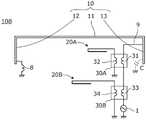
图24是表示第8实施方式所涉及的天线装置108的电路结构的图。FIG. 24 is a diagram showing a circuit configuration of the
图25是表示第9实施方式所涉及的天线装置109的电路结构的图。FIG. 25 is a diagram showing a circuit configuration of the
图26是表示第10实施方式所涉及的天线装置110的电路结构的图。FIG. 26 is a diagram showing a circuit configuration of the
图27的(A)、图27的(B)是表示第11实施方式所涉及的天线装置111A、111B的电路结构的图。27(A) and 27(B) are diagrams showing circuit configurations of
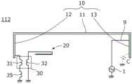
图28是表示第12实施方式所涉及的天线装置112的电路结构的图。FIG. 28 is a diagram showing a circuit configuration of the
图29是表示第13实施方式所涉及的天线装置113的电路结构的图。FIG. 29 is a diagram showing a circuit configuration of the
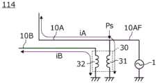
图30是表示第14实施方式所涉及的天线装置114的电路结构的图。FIG. 30 is a diagram showing a circuit configuration of the
图31的(A)是表示第15实施方式所涉及的天线装置115的电路结构的图。图31的(B)是表示图31的(A)所示的天线装置115、比较例的天线装置和它们的反射损耗的频率特性的图。FIG. 31(A) is a diagram showing a circuit configuration of the
图32是表示第16实施方式所涉及的天线装置116的电路结构的图。FIG. 32 is a diagram showing a circuit configuration of the
图33是表示第17实施方式所涉及的天线装置117的电路结构的图。FIG. 33 is a diagram showing a circuit configuration of the
图34是表示天线装置117的反射损耗的频率特性的图。FIG. 34 is a graph showing frequency characteristics of the return loss of the
图35是第18实施方式所涉及的天线装置118A的电路图。FIG. 35 is a circuit diagram of an
图36是第18实施方式所涉及的其它的天线装置118B的电路图。FIG. 36 is a circuit diagram of another
图37是第18实施方式所涉及的又一天线装置118C的电路图。FIG. 37 is a circuit diagram of still another
图38是第19实施方式所涉及的天线装置119的主要部分的俯视图。FIG. 38 is a plan view of the main part of the
图39是第19实施方式的耦合电路30的立体图。FIG. 39 is a perspective view of the
图40是表示第19实施方式的另一耦合电路30的结构的图,是表示形成于耦合电路30的各层的导体图案的分解俯视图。FIG. 40 is a diagram showing the configuration of another
图41是供电电路1所连接的第20实施方式所涉及的天线装置120的电路图。FIG. 41 is a circuit diagram of the
图42是将第20实施方式所涉及的移相器50分为理想变压器IT和寄生电感成分来表示的等效电路图。FIG. 42 is an equivalent circuit diagram showing the
图43是表示移相器50的移相量的频率特性的图。FIG. 43 is a graph showing the frequency characteristic of the phase shift amount of the
图44的(A)是不具备移相器50的第1实施方式中所示的天线装置的电路图,图44的(B)是在史密斯圆图上表示从供电电路1观察该天线装置的阻抗的阻抗轨迹。FIG. 44(A) is a circuit diagram of the antenna device shown in the first embodiment without the
图45的(A)是追加了移相器50的天线装置的电路图,图45的(B)是在史密斯圆图上表示从供电电路1观察该天线装置的阻抗的阻抗轨迹。FIG. 45(A) is a circuit diagram of the antenna device to which the
图46的(A)是具备阻抗匹配用电容器C5的天线装置的电路图,图46的(B)是在史密斯圆图上表示从供电电路1观察该天线装置的阻抗的阻抗轨迹。FIG. 46(A) is a circuit diagram of the antenna device including the impedance matching capacitor C5 , and FIG. 46(B) is an impedance locus showing the impedance of the antenna device viewed from the
图47是表示图44的(A)、图46的(A)所示的各天线装置以及比较例的天线装置的反射损耗的频率特性的图。FIG. 47 is a graph showing frequency characteristics of the return loss of each of the antenna devices shown in FIG. 44(A) and FIG. 46(A) and the antenna device of the comparative example.
图48是移相器50的外观立体图。FIG. 48 is an external perspective view of the
图49是移相器50的各层的俯视图。FIG. 49 is a plan view of each layer of the
图50是移相器50的剖视图。FIG. 50 is a cross-sectional view of the
图51是表示第21实施方式所涉及的电子设备的金属壳体的一部分的俯视图。51 is a plan view showing a part of a metal case of the electronic device according to the twenty-first embodiment.
图52的(A)(B)是表示第21实施方式所涉及的分别不同的电子设备的金属壳体的一部分的立体图。(A) (B) of FIG. 52 is a perspective view which shows a part of the metal case of each different electronic device which concerns on 21st Embodiment.
-符号说明--Symbol Description-
C、C1...电容C, C1...capacitor
C3、C4...电容器C3, C4...Capacitors
C5...阻抗匹配用电容器C5... Impedance matching capacitor
C11、C12...电容形成用导体图案C11, C12...conductor pattern for capacitor formation
C20...电容器C20...capacitor
Cs1、Cs2...电容器(寄生电容)Cs1, Cs2...Capacitors (Parasitic Capacitance)
G...接地端子G...ground terminal
GND...接地电极GND...ground electrode
GZ...接地区域GZ...ground zone
IT...理想变压器IT...the ideal transformer
L1A1、L1A2、L1A3、L1B1、L1B2、L1C...导体L1A1, L1A2, L1A3, L1B1, L1B2, L1C... conductors
L2A1、L2A2、L2A3、L2B1、L2B2、L2C...导体L2A1, L2A2, L2A3, L2B1, L2B2, L2C... conductors
La、Lc...串联寄生电感成分La, Lc... series parasitic inductance components
Lb...并联寄生电感成分Lb...parasitic inductance component in parallel
Lp...第1线圈Lp...1st coil
Ls...第2线圈Ls...2nd coil
L11...第1导体图案L11...1st conductor pattern
L12...第2导体图案L12...2nd conductor pattern
L20...电感器L20...inductor
L21...第3导体图案L21...3rd conductor pattern
L22...第4导体图案L22...4th conductor pattern
L21~L23...导体图案L21~L23...Conductor pattern
L3...电感器L3...inductor
MS1...第1面MS1...
MS2...第2面MS2...
NGZ...非接地区域NGZ...non-grounded area
PA...辐射元件连接端子PA...radiating element connection terminal
PF...供电电路连接端子PF...Power supply circuit connection terminal
PG...接地端子PG...ground terminal
PS...非辐射性谐振电路连接端子PS...Non-radiative resonance circuit connection terminal
Ps...连接点Ps...connect the dots
P1...第1端口P1...
P2...第2端口P2...
S1~S9...基材S1~S9...Substrate
S11、S12、S21、S22、S23...绝缘基材S11, S12, S21, S22, S23...Insulation substrate
T1、T2...端子T1, T2... Terminals
V1、V2...层间连接导体V1, V2...Interlayer connecting conductors
V11、V12、V13、V14、V21、V22、V23、V24...层间连接导体V11, V12, V13, V14, V21, V22, V23, V24... Interlayer connecting conductors
1...供电电路1...Power supply circuit
5...基板5...Substrate
6...电路基板6...Circuit substrate
7...连接器7...connector
8...电感器8...Inductors
9...供电线路9...Power supply line
10...辐射元件10...radiating element
10A...供电辐射元件10A...Powered radiating element
10AF...供电路径10AF...supply path
10AS...短路管脚10AS...short circuit pin
10B、10C...无供电辐射元件10B, 10C... Unpowered radiating element
10U、10V...供电辐射元件10U, 10V... power radiating element
10Z...辐射元件形成区域10Z...radiating element forming area
11...端面部11...End face
12、13...侧面部12, 13...side part
20...非辐射性谐振电路20...Non-radiative resonant circuit
20A...第1非辐射性谐振电路20A...1st non-radiative resonant circuit
20B...第2非辐射性谐振电路20B...2nd non-radiative resonant circuit
20FB...折回部20FB...return section
21...第1线状导体图案部21...1st linear conductor pattern part
22...第2线状导体图案部22...2nd linear conductor pattern part
30...耦合电路30...Coupling circuit
30A...第1耦合电路30A...1st coupling circuit
30B...第2耦合电路30B...2nd coupling circuit
31...第1耦合元件31...1st coupling element
32...第2耦合元件32...2nd coupling element
33...第3耦合元件33...3rd coupling element
34...第4耦合元件34...4th coupling element
35...电感器35...Inductors
36...电容器36...Capacitor
37、38...开关37, 38... switch
40...金属壳体主要部分40...The main part of the metal shell
41...平面部41...Flat part
42、43...侧面部42, 43...side part
50...移相器50...Phase shifter
100...层叠体100...Laminate
101~105...天线装置101~105...Antenna device
106A~106D...天线装置106A~106D...Antenna device
107A、107B...天线装置107A, 107B...Antenna device
108~110...天线装置108~110...Antenna device
111A、111B...天线装置111A, 111B...Antenna device
112~117...天线装置112~117...Antenna device
118A~118C...天线装置118A~118C...Antenna device
119、120...天线装置。119, 120...Antenna device.
具体实施方式Detailed ways
以下,参照附图来举出几个具体的例子,表示本发明的多个具体实施方式。各附图中对同一位置赋予同一符号。考虑要点的说明或者理解的容易性,为了方便而分开实施方式进行表示,但能够进行不同实施方式中所示的结构的局部置换或者组合。在第2实施方式以后,省略与第1实施方式共用的事项的记述,仅对不同点进行说明。特别地,针对基于相同结构的相同的作用效果,不按照每个实施方式依次提及。Hereinafter, several specific examples are given with reference to the drawings, and several specific embodiments of the present invention are shown. In each drawing, the same symbol is assigned to the same position. In consideration of the ease of explanation or understanding of the main points, the embodiments are shown separately for convenience, but partial replacements or combinations of the structures shown in different embodiments are possible. After the second embodiment, descriptions of matters common to the first embodiment are omitted, and only the differences will be described. In particular, for the same effect based on the same structure, it will not be mentioned in sequence according to each embodiment.
各实施方式所示的“天线装置”能够应用于信号的发送侧、接收侧的任意侧。即便在将该“天线装置”说明为辐射电磁波的天线的情况下,也并不局限于该天线装置是电磁波的产生源。在受到通信对象侧天线装置产生的电磁波的情况下,也就是即便收发的关系相反,也起到相同的作用效果。The "antenna device" described in each embodiment can be applied to any of the signal transmission side and the reception side. Even when the "antenna device" is described as an antenna that radiates electromagnetic waves, it is not limited that the antenna device is a generator of electromagnetic waves. In the case of receiving the electromagnetic wave generated by the antenna device on the communication partner side, that is, even if the relationship of transmission and reception is reversed, the same effect is obtained.
《第1实施方式》"First Embodiment"
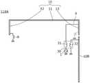
图1是表示第1实施方式所涉及的天线装置101和具备其的电子设备的主要结构的立体图。图2是天线装置101的主要部分的俯视图。FIG. 1 is a perspective view showing a main configuration of an
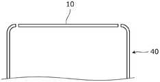
电子设备的金属壳体具备作为金属壳体端部的辐射元件10和金属壳体主要部分40。金属壳体主要部分40由平面部41、侧面部42、43构成。The metal case of the electronic device includes a radiating
天线装置101具备:辐射元件10、非辐射性谐振电路20和耦合电路30。The
辐射元件10是金属壳体端部,由端面部11、侧面部12、13构成。侧面部12的端部经由电感器8而与电路基板6的接地连接(接地)。侧面部13的端部开放,但在该开放端与接地之间产生寄生电容C。另外,在电路基板6安装USB等连接器7,在端面部11形成用于连接器7的开口,但该连接器7不是天线装置101的构成要素。The
电路基板6具有:形成有接地电极GND的接地区域GZ、和未形成有接地电极的非接地区域NGZ。作为辐射元件10的金属壳体端部位于非接地区域的一侧。在电路基板6的非接地区域NGZ,形成基于导体图案的非辐射性谐振电路20。此外,在电路基板6的非接地区域NGZ,形成将耦合电路30与辐射元件10连接的供电线路9。The
如图2所示,非辐射性谐振电路20由在中途具有折回部20FB的线状的导体图案构成。这样,通过由在中途具有折回部的线状的导体图案构成,非辐射性谐振电路20被省空间地设置,此外,能够得到谐振所需的电长度。此外,在本实施方式中,具有从耦合电路30延伸的第1线状导体图案部21、和折回到远离辐射元件10的一侧的第2线状导体图案部22。通根据该构造,接近于辐射元件10(特别是端面部11)的部分较短,并且延伸方向相互为相反方向,因此与辐射元件10(特别是端面部11)的实质的耦合较小。由此,非辐射性谐振电路20与辐射元件10的不必要的耦合被抑制。As shown in FIG. 2 , the
另外,由于第2线状导体图案部22的线宽比第1线状导体图案部21粗,因此能够加宽谐振的带宽。In addition, since the line width of the second linear
图3是表示非辐射性谐振电路20的形成位置的俯视图。辐射元件10由俯视情况下形成3边的导电性部件(端面部11、侧面部12、13)构成,非辐射性谐振电路20位于俯视情况下辐射元件10的3边围起的辐射元件形成区域10Z内。非辐射性谐振电路20也可以不是其全体位于辐射元件形成区域10Z内,优选非辐射性谐振电路20的一半以上处于辐射元件形成区域10Z内。由于非辐射性谐振电路20不利用为辐射元件,因此优选是“非辐射性”。因此,通过非辐射性谐振电路20处于俯视情况下导电性部件的3边围起的位置、或非辐射性谐振电路20的一半以上处于辐射元件形成区域10Z内,从而非辐射性谐振电路20被辐射元件10遮挡,因此从远处观察到的非辐射性谐振电路20的非辐射性提高。FIG. 3 is a plan view showing the formation position of the
图4是表示耦合电路30和与其连接的电路的结构的图。耦合电路30具有第1耦合元件31和与第1耦合元件31耦合的第2耦合元件32,由第1耦合元件31和第2耦合元件32构成变压器。第1耦合元件31以及第2耦合元件32的电感较小,分别为10nH以下。辐射元件10与非辐射性谐振电路20经由耦合电路30,以耦合系数0.5以上、优选以耦合系数0.8以上进行耦合。耦合元件的电感越小,对辐射元件10的电路特性以及辐射特性的影响越能够被抑制。耦合系数越大,越能够将辐射元件10与非辐射性谐振电路20电连接,仅在较大有助于非辐射性谐振电路20谐振的频率施加谐振点。这样,通过构成第1耦合元件31与第2耦合元件32电磁场耦合的变压器,从而构成第1耦合元件31与第2耦合元件32的耦合系数较高的耦合电路,从供电电路1观察辐射元件10时的非辐射性谐振电路20的谐振特性容易显现。FIG. 4 is a diagram showing the configuration of the
第1耦合元件31被连接于辐射元件10与供电电路1之间。第2耦合元件32的第1端与非辐射性谐振电路20连接,第2端与电路基板6的接地连接(接地)。The
根据本实施方式的电子设备,由于将收容供电电路的壳体的金属部利用为辐射元件,因此不需要设置辐射元件专用的导电性部件或导体图案,能够实现小型化。此外,在具备金属壳体的电子设备中,也不会被金属壳体遮挡。According to the electronic device of the present embodiment, since the metal portion of the housing housing the power supply circuit is used as the radiation element, it is not necessary to provide a conductive member or conductor pattern dedicated to the radiation element, and miniaturization can be achieved. In addition, even in an electronic device having a metal case, it is not blocked by the metal case.
图5的(A)是高频带下的天线装置101的等效电路图。在高频带(例如1.6GHz~2.3GHz)下,电感器8(参照图2、图4)为给定的高阻抗,辐射元件10的前端等效为开放状态。在该状态下,辐射元件10作为以3/4波长或者(2n+1)/4波长(n为自然数)进行谐振的单极系天线而发挥作用。FIG. 5(A) is an equivalent circuit diagram of the
图5的(B)是低频带下的天线装置101的等效电路图。在低频带(例如700MHz~900MHz)下,电感器8表示给定的电感,辐射元件10的前端经由电感器8而接地。在该状态下,辐射元件10作为1波长或者其整数倍波长的环状天线而发挥作用。FIG. 5(B) is an equivalent circuit diagram of the
基于图5的(A)(B)所示的电感器L20以及电容器C20的串联电路是用于表示为将非辐射性谐振电路20简单表述为集中常量电路的等效电路的元件。非辐射性谐振电路20作用为在给定频率下以3/4波长或者(2n+1)/4波长(n为自然数)进行谐振的开路端短截线。因此,在图5的(A)(B)中表示为电感器L20以及电容器C20。非辐射性谐振电路20例如在以2.1GHz为中心的频带下进行谐振。其中,在本实施方式中,由于非辐射性谐振电路20是线状导体图案在中途折回的形状,因此与单纯的直线状的导体图案相比,在线状导体图案不形成显著的驻波,作为谐振电路的谐振的Q值较小。The series circuit based on the inductor L20 and the capacitor C20 shown in (A) and (B) of FIG. 5 is an element for expressing the
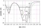
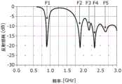
图6是针对天线装置101和比较例的天线装置,表示其反射损耗的频率特性的图。在图6中,反射损耗特性RL1是本实施方式的天线装置101的反射损耗,反射损耗特性RL2是比较例的天线装置的反射损耗。比较例的天线装置是不具备耦合电路30以及非辐射性谐振电路20的天线装置。在任意天线装置中,均在低频带(700MHz~900MHz)的中心频率F1产生极点。这是由于图5的(B)所示的环状天线的谐振特性。此外,在频率F2(1.75GHz附近)产生极点。这是由于图5的(A)所示的单极天线的3/4波长谐振。进一步地,在频率F3(2.3GHz附近)产生极点。这是由于图5的(A)所示的单极天线的5/4波长谐振。FIG. 6 is a diagram showing frequency characteristics of the return loss of the
另外,优选图4所示的第1耦合元件31与供电电路1之间的线路的长度“r1”以及第2耦合元件32的端部与接地之间的线路的长度“r2”小于谐振频率的1/8波长。所谓这里的波长,包含考虑了基于磁性体、电介质的波长缩短效果的实效波长的意思。将“1/8波长”设为阈值,是基于1/8波长电流为1/√2、换言之能够传输的电力为一半、且在条件上实用。In addition, it is preferable that the length “r1” of the line between the
这里,针对基于上述耦合强度的阻抗匹配的差异,图7中表示概念图。在图7中,轨迹T0、T1、T2是在史密斯圆图上表示从供电电路1观察天线装置101的阻抗的阻抗轨迹。轨迹T0是不存在耦合电路30以及非辐射性谐振电路20的状态下的特性,轨迹T1是耦合电路30的第1耦合元件31与第2耦合元件32适度地耦合的状态下的特性,轨迹T2是耦合电路30的第1耦合元件31与第2耦合元件32的耦合过强的状态下的特性。Here, FIG. 7 shows a conceptual diagram of the difference in impedance matching based on the coupling strength described above. In FIG. 7 , the traces T0 , T1 , and T2 are impedance traces showing the impedance of the
这样,即便耦合电路30的第1耦合元件31与第2耦合元件32的耦合过强,从供电电路观察的输入阻抗也从供电电路(以及传输线路)侧的阻抗(例如50Ω)偏离。因此,耦合电路30的第1耦合元件31与第2耦合元件32适度地耦合很重要。通过上述第1耦合元件31与供电电路1之间的线路的长度“r1”以及第2耦合元件32的端部与接地之间的线路的长度“r2”在小于谐振频率的1/8波长的范围内规定,从而能够适度地规定基于耦合电路30的耦合。In this way, even if the coupling between the
在本实施方式的天线装置101中,在频率F0(2.1GHz附近)也产生极点。这是由于非辐射性谐振电路20的谐振特性。也就是说,由于非辐射性谐振电路20以中心频率2.1GHz的频带进行谐振,因此在从供电电路1观察的天线装置101的反射损耗的频率特性,以该2.1GHz产生极点。根据本实施方式的天线装置101,在1.6GHz~2.3GHz,高频带的应用频带被宽频带化。In the
此外,在低频带中非辐射性谐振电路20不谐振,对低频带的反射损耗特性没有影响。换句话说,在从供电电路1观察的反射损耗特性,在例如1.6GHz以上的频带,非辐射性谐振电路20有影响,在低于此的频带,非辐射性谐振电路20实质没有影响。In addition, the
由于上述频率F0附近的反射损耗的特性根据非辐射性谐振电路20的谐振特性而被规定,因此根据构成非辐射性谐振电路20的导体图案的形状,能够适当地给定频率F0附近的反射损耗的特性。在本实施方式中,由于非辐射性谐振电路20由在中途具有折回部的线状的导体图案构成,因此非辐射性谐振电路20的谐振的锐利性变缓,通过非辐射性谐振电路20,包含在上述频率F0产生的极点的该附近频带,能够使反射系数较宽衰减。Since the characteristics of the reflection loss in the vicinity of the frequency F0 are defined by the resonance characteristics of the
另外,由于作用为开路端短截线的非辐射性谐振电路20被与辐射元件10实质独立地设置,因此与例如在辐射元件形成短截线的情况相比,没有针对低频带的影响。In addition, since the non-radiative
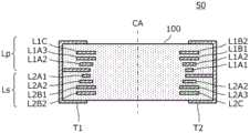
接下来,表示耦合电路30的结构。图8是耦合电路30的立体图,图9是表示形成于耦合电路的各层的导体图案的分解俯视图。Next, the configuration of the
本实施方式的天线装置所具备的耦合电路30是被安装于电路基板6的长方体状的芯片部件。在图8中,将耦合电路30的外形和其内部的构造分离图示。耦合电路30的外形通过双点划线来表示。在耦合电路30的外表面,形成供电电路连接端子PF、辐射元件连接端子PA、接地端子PG以及非辐射性谐振电路连接端子PS。此外,耦合电路30具备:第1面MS1、和作为与该第1面相反的一侧的面的第2面MS2。在本实施方式中,第1面MS1是安装面,该面与电路基板对置。对作为与安装面(第1面)MS1相反的一侧的面的顶面(第2面),赋予方向识别标记DDM。该方向识别标记DDM例如被利用于在针对耦合电路30通过安装机来将芯片部件安装于电路基板时,检测芯片部件的方向。The
在耦合电路30的内部,形成第1导体图案L11、第2导体图案L12、第3导体图案L21、第4导体图案L22。第1导体图案L11与第2导体图案L12经由层间连接导体V1而连接。第3导体图案L21与第4导体图案L22经由层间连接导体V2而连接。另外,在图8中,将形成有上述各导体图案的绝缘基材S11、S12、S21、S22在层叠方向上分离表示。这些绝缘基材S11、S12、S21、S22可以是由LTCC(Low Temperature Co-fired Ceramics:低温共烧陶瓷)等构成的非磁性陶瓷层叠体,也可以是由聚酰亚胺或液晶聚合物等的树脂材料构成的树脂层叠体。这样,通过基材层是非磁性体(由于不是磁性体铁氧体),从而即便是超过几百MHz的高频带也能够用作为耦合电路。Inside the
上述各导体图案以及层间连接导体由以Ag或Cu为主成分的电阻率较小的导体材料构成。若基材层是陶瓷,则通过例如以Ag或Cu为主成分的导电性膏的丝网印刷以及烧成而形成。此外,若基材层是树脂,则通过例如Al箔或Cu箔等金属箔利用蚀刻等而被图案化而形成。Each of the conductor patterns and the interlayer connection conductors described above is formed of a conductor material with a low resistivity mainly composed of Ag or Cu. When the base material layer is a ceramic, it is formed by, for example, screen printing and firing of a conductive paste containing Ag or Cu as a main component. Moreover, when a base material layer is resin, it is formed by patterning metal foil, such as Al foil and Cu foil, by etching etc., for example.
如图9所示,从接近于安装面的层起依次形成第1导体图案L11、第2导体图案L12、第3导体图案L21、第4导体图案L22。第1导体图案LI1的第1端与辐射元件连接端子PA连接,第2端经由层间连接导体V1而与第2导体图案L12的第1端连接。第2导体图案L12的第2端与供电电路连接端子PF连接。此外,第3导体图案L21的第1端与非辐射性谐振电路连接端子PS连接,第3导体图案L21的第2端经由层间连接导体V2而与第4导体图案L22的第1端连接。第4导体图案L22的第2端与接地端子PG连接。As shown in FIG. 9, the 1st conductor pattern L11, the 2nd conductor pattern L12, the 3rd conductor pattern L21, and the 4th conductor pattern L22 are formed in this order from the layer close|similar to the mounting surface. The first end of the first conductor pattern LI1 is connected to the radiation element connection terminal PA, and the second end is connected to the first end of the second conductor pattern L12 via the interlayer connection conductor V1. The second end of the second conductor pattern L12 is connected to the power supply circuit connection terminal PF. In addition, the first end of the third conductor pattern L21 is connected to the non-radiative resonance circuit connection terminal PS, and the second end of the third conductor pattern L21 is connected to the first end of the fourth conductor pattern L22 via the interlayer connection conductor V2. The second end of the fourth conductor pattern L22 is connected to the ground terminal PG.
此外,从第1耦合元件31的供电电路连接端子PF向辐射元件连接端子PA的卷绕方向与从第2耦合元件32的非辐射性谐振电路连接端子PS向接地端子PG的卷绕方向相反。换句话说,第1耦合元件31中从供电电路连接端子PF向辐射元件连接端子PA的方向上流过电流时产生的磁场(磁通)与第2耦合元件32中从非辐射性谐振电路连接端子PS向接地端子PG的方向上流过电流时产生的磁场(磁通)相互削弱。这里,在辐射元件连接端子PA作为单极天线而谐振时,经由供电电路1以及接地电极GND而连接的耦合电路30中的第1耦合元件31与第2耦合元件32的极性相互相反,第1耦合元件31中从供电电路连接端子PF向辐射元件连接端子PA流过电流,第2耦合元件32中从非辐射性谐振电路连接端子PS向接地端子PG流过电流,产生的磁场(磁通)相互削弱。由此,第1耦合元件31以及第2耦合元件32的电感比基于第1耦合元件31与第2耦合元件32的耦合的互感低,对辐射元件10的电路特性以及辐射特性的影响较小。In addition, the winding direction from the feeding circuit connection terminal PF of the
图10是包含上述4个线圈导体图案的耦合电路30的电路图。第2导体图案L12与第1导体图案L11串联连接并构成第1耦合元件31。同样地,第4导体图案L22与第3导体图案L21串联连接并构成第2耦合元件32。第2导体图案L12与第3导体图案L21在层叠方向相邻,该第2导体图案L12与第3导体图案L21的磁场耦合特别强,因此在图10中,使其相邻并描绘。当然,第2导体图案L12以及第1导体图案L11分别与第4导体图案L22以及第3导体图案L21磁场耦合。FIG. 10 is a circuit diagram of a
在图9所示的例子中,在第2导体图案L12的一部分形成电容形成用导体图案C11,在第3导体图案L21的一部分形成电容形成用导体图案C12。因此,如图10所示,在第2导体图案L12的中途与非辐射性谐振电路连接端子PS之间构成电容C1。该电容C1作为供电电路1与非辐射性谐振电路20的阻抗匹配电路而发挥作用。In the example shown in FIG. 9, the conductor pattern C11 for capacitor|condenser formation is formed in a part of 2nd conductor pattern L12, and the conductor pattern C12 for capacitor|condenser formation is formed in a part of 3rd conductor pattern L21. Therefore, as shown in FIG. 10 , a capacitor C1 is formed between the middle of the second conductor pattern L12 and the non-radiative resonance circuit connection terminal PS. The capacitor C1 functions as an impedance matching circuit between the
《第2实施方式》"Second Embodiment"
图11是表示第2实施方式所涉及的天线装置102的电路结构的图。该天线装置102在耦合电路30的第2耦合元件32与非辐射性谐振电路20之间连接(插入)电感器35。其他的结构与第1实施方式中图4所示的电路相同。FIG. 11 is a diagram showing a circuit configuration of the
根据本实施方式,由于在电流较小的位置插入电感器35,因此能够抑制耦合电路30的耦合的变化并且降低非辐射性谐振电路20的谐振频率,能够得到所希望的通信频带。或者,能够维持谐振频率并且缩短非辐射性谐振电路20的长度,实现省空间化。According to the present embodiment, since the
另外,上述电感器35也可以与耦合电路30一体化。其中,优选构成为不与第1耦合元件31耦合。In addition, the above-mentioned
《第3实施方式》"Third Embodiment"
图12是表示第3实施方式所涉及的天线装置103的电路结构的图。该天线装置103在耦合电路30的第2耦合元件32与接地之间连接(插入)电感器35。其他的结构与第1实施方式中图4所示的电路相同。FIG. 12 is a diagram showing a circuit configuration of the
若对天线装置附加耦合电路30,则在接地与耦合电路30之间产生寄生电容。根据本实施方式,通过上述电感器35与上述寄生电容谐振,能够抑制电抗成分。因此,通过在通过对天线装置附加耦合电路30来不希望使天线特性变化的频带,插入与上述寄生电容谐振的电感的电感器35,能够抑制从未安装耦合电路30的状态下的匹配状态发生的变化。When the
此外,通过电感器35的插入能够降低非辐射性谐振电路20的谐振频率,能够得到所希望的通信频带、通信特性。或者能够维持谐振频率并且缩短天线的长度,空间被抑制。In addition, by inserting the
另外,上述电感器35也可以与耦合电路30一体化。其中,优选构成为不与第1耦合元件31耦合。In addition, the above-mentioned
《第4实施方式》"Fourth Embodiment"
图13是表示第4实施方式所涉及的天线装置104的电路结构的图。该天线装置104在耦合电路30的第2耦合元件32与非辐射性谐振电路20之间连接(插入)电容器36。其他的结构与第1实施方式中图4所示的电路相同。FIG. 13 is a diagram showing a circuit configuration of the
根据本实施方式,能够提高非辐射性谐振电路侧的谐振频率,能够得到所希望的通信频带。According to this embodiment, the resonance frequency on the non-radiative resonance circuit side can be increased, and a desired communication frequency band can be obtained.
另外,上述电容器36也可以与耦合电路30一体化。In addition, the above-mentioned
《第5实施方式》"Fifth Embodiment"
图14是表示第5实施方式所涉及的天线装置105的电路结构的图。该天线装置105在耦合电路30的第2耦合元件32与接地之间连接(插入)电容器36。其他的结构与第1实施方式中图4所示的电路相同。FIG. 14 is a diagram showing the circuit configuration of the
根据本实施方式,能够减弱由于插入耦合电路30所导致的接地与耦合电路30之间的寄生电容(合成电容被减少),能够抑制自未安装耦合电路30的状态下的匹配状态起的变化。此外,能够提高非辐射性谐振电路20的谐振频率,得到所希望的通信频带、通信特性。According to the present embodiment, the parasitic capacitance between the ground and the
另外,上述电容器36也可以与耦合电路30一体化。In addition, the above-mentioned
《第6实施方式》"Sixth Embodiment"
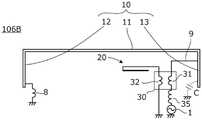
图15是表示第6实施方式所涉及的天线装置106A的电路结构的图。该天线装置106A在耦合电路30的第1耦合元件31与辐射元件10之间连接(插入)电感器35。其他的结构与第1实施方式中图6所示的电路相同。FIG. 15 is a diagram showing a circuit configuration of an
根据天线装置106A的结构,由于在作为电流比插入的电感器35强的一侧的供电侧存在第1耦合元件31,因此能够维持提供给非辐射性谐振电路20的电力比,并且改变辐射元件10的谐振频率,或者调整阻抗匹配的程度。此外,由于通过基于第1耦合元件31、第2耦合元件32的电感、第1耦合元件31与第2耦合元件32之间产生的寄生电容而规定的自谐振频率难以降低,因此自谐振频率不会对通信频带下的使用有负面影响。换句话说,在自谐振的状态下,其频带的能量将变为接地并不辐射,但若自谐振频率为比通信频带高的状态,则不产生这种问题。According to the configuration of the
图16是表示第6实施方式所涉及的天线装置106B的电路结构的图。该天线装置106B在耦合电路30的第1耦合元件31与供电电路1之间连接(插入)电感器35。其他的结构与第1实施方式中图4所示的电路相同。FIG. 16 is a diagram showing a circuit configuration of an
根据天线装置106B的结构,由于耦合电路30的第1耦合元件31被插入到电流比电感器35的位置弱的一侧,因此与在辐射元件10与第1耦合元件31之间插入电感器的情况相比,能够适度地调整通过耦合电路30以及非辐射性谐振电路20而附加的谐振下的(谐振频率下的)阻抗匹配的程度。具体而言,能够避免输入阻抗过度变化并且阻抗匹配偏离这一状况。According to the configuration of the
此外,由于通过电感器35的插入,能够降低耦合电路30的自谐振频率,因此通过将上述自谐振频率规定为不希望使其辐射的频带,能够抑制不必要的辐射。In addition, since the self-resonant frequency of the
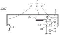
图17是表示第6实施方式所涉及的天线装置106C的电路结构的图。该天线装置106C在耦合电路30的第1耦合元件31与辐射元件10之间连接(插入)电容器36。其他的结构与第1实施方式中图6所示的电路相同。FIG. 17 is a diagram showing a circuit configuration of an
根据天线装置106C的结构,能够通过插入的电容器36的电容来调整辐射元件10的谐振频率,或者调整阻抗匹配的程度。Depending on the configuration of the
图18是表示第6实施方式所涉及的天线装置106D的电路结构的图。该天线装置106D在耦合电路30的第1耦合元件31与供电电路1之间连接(插入)电容器36。其他的结构与第1实施方式中图4所示的电路相同。FIG. 18 is a diagram showing a circuit configuration of an
根据天线装置106D的结构,能够通过插入的电容器36的电容来调整辐射元件10的谐振频率,或者调整阻抗匹配的程度。此外,由于在供电电路1与第1耦合元件31之间插入电容器36,因此成为在第1耦合元件31与第2耦合元件32之间产生的寄生电容与电容器36串联连接的构造。因此,自谐振电路系统中包含的合成电容降低,自谐振频率变高。由此,能够使自谐振频率从使用的通信频带偏离。Depending on the configuration of the
《第7实施方式》"Seventh Embodiment"
图19的(A)是表示第7实施方式所涉及的天线装置107A的电路结构的图,图19的(B)是表示第7实施方式所涉及的天线装置107B的电路结构的图。这些天线装置107A、107B的结构与第1实施方式中图4所示的电路相同。其中,在将耦合电路30的第1耦合元件31的自感表示为L1、将第2耦合元件32的自感表示为L2时,设置于天线装置107A的耦合电路30的第1耦合元件31、第2耦合元件32处于L2>L1的关系,在天线装置107B中,处于L2<L1的关系。若处于L2>L1的关系,则与L1=L2的情况相比,能够降低非辐射性谐振电路20的谐振频率。或者,若在相同的谐振频率下进行比较,则能够缩短非辐射性谐振电路20。FIG. 19(A) is a diagram showing the circuit configuration of the
此外,在L2>L1的情况下,与在耦合电路30的外侧在第2耦合元件32连接(附加)电感器的结构相比,相对较大的自感的第2耦合元件32整体有助于与第1耦合元件31的耦合,因此能够增大提供给非辐射性谐振电路20的电力比。In addition, in the case of L2>L1, the relatively large self-inductance of the
此外,在L2<L1的情况下,与在耦合电路30的外侧在第1耦合元件31连接(附加)电感器的结构相比,相对较大的自感的第1耦合元件31整体有助于与第2耦合元件32的耦合,因此能够增大提供给非辐射性谐振电路20的电力比。In addition, in the case of L2<L1, the relatively large self-inductance of the
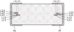
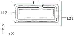
图20是表示形成于本实施方式所涉及的耦合电路30的各层的导体图案的分解俯视图。本实施方式的天线装置所具备的耦合电路30是被安装于电路基板的长方体状的芯片部件。FIG. 20 is an exploded plan view showing conductor patterns formed in each layer of the
在绝缘基材S11、S12、S21、S22,S23,分别形成导体图案L11、L12、L21、L22、L23。导体图案L11的第1端与辐射元件连接端子PA连接,第2端经由层间连接导体V1来与导体图案L12的第1端连接。导体图案L12的第2端与供电电路连接端子PF连接。导体图案L21的第1端与非辐射性谐振电路连接端子PS连接,第2端经由层间连接导体V21来与导体图案L22的第1端连接。导体图案L22的第2端经由层间连接导体V22来与导体图案L23的第1端连接。并且,导体图案L23的第2端与接地端子PG连接。Conductor patterns L11, L12, L21, L22, and L23 are formed on the insulating base materials S11, S12, S21, S22, and S23, respectively. The first end of the conductor pattern L11 is connected to the radiation element connection terminal PA, and the second end is connected to the first end of the conductor pattern L12 via the interlayer connection conductor V1. The second end of the conductor pattern L12 is connected to the power supply circuit connection terminal PF. The first end of the conductor pattern L21 is connected to the non-radiative resonance circuit connection terminal PS, and the second end is connected to the first end of the conductor pattern L22 via the interlayer connection conductor V21. The second end of the conductor pattern L22 is connected to the first end of the conductor pattern L23 via the interlayer connection conductor V22. In addition, the second end of the conductor pattern L23 is connected to the ground terminal PG.
图21是上述耦合电路30的剖视图。图22是特别表示导体图案L12与导体图案L21的重叠的俯视图。构成第1耦合元件31的导体图案L11、L12的线圈开口或者线圈直径比构成第2耦合元件32的导体图案L21、L22、L23的线圈开口或者线圈直径小。此外,导体图案L11、L12与导体图案L21、L22、L23的线宽的一部分重叠。在图21、图22所示的例子中,在整周上大约仅1/2的宽度重叠。FIG. 21 is a cross-sectional view of the
图23是表示第7实施方式所涉及的形成于另一耦合电路30的各层的导体图案的分解俯视图。各导体图案的形状和大小与图20所示的例子不同。图23所示的耦合电路的各导体图案之中,构成第1耦合元件31的导体图案L11、L12的线圈外径比构成第2耦合元件32的导体图案L21、L22、L23的线圈内径小。FIG. 23 is an exploded plan view showing conductor patterns formed in each layer of the
根据图20~图23所示的结构,在构成第1耦合元件31的导体图案(L11、L12)与构成第2耦合元件32的导体图案(L21、L22、L23)之间产生的寄生电容被抑制。因此,通过基于第1耦合元件31、第2耦合元件32的电感和上述寄生电容而规定的自谐振频率变高,能够将自谐振频率从使用通信频带偏离。此外,即便存在构成第1耦合元件31的导体图案(L11、L12)与构成第2耦合元件32的导体图案(L21、L22、L23)的面方向(图22所示的X-Y面方向)的位置偏移,第1耦合元件31的线圈开口与第2耦合元件32的线圈开口重叠的部分也保持一定,因此第1耦合元件31与第2耦合元件32的磁场耦合的耦合度相对于构成第1耦合元件31的导体图案(L11、L12)与构成第2耦合元件32的导体图案(L21、L22、L23)的面方向的位置偏移的变化较小。According to the structures shown in FIGS. 20 to 23 , the parasitic capacitances generated between the conductor patterns ( L11 , L12 ) constituting the
图20、图23的任意例子均为处于上述L1<L2的关系的耦合电路的例子。在设为L1>L2的情况下,由线圈开口相对较大的导体图案构成第1耦合元件31即可。Each of the examples in FIGS. 20 and 23 is an example of a coupling circuit in the above-described relationship of L1<L2. In the case of L1>L2, the
另外,在图20、图23中,表示了缓和针对构成第1耦合元件31的导体图案(L11、L12)与构成第2耦合元件32的导体图案(L21、L22、L23)的位置偏移的影响的例子,同样地,也能够缓和针对构成第1耦合元件31的各导体图案彼此的面方向的位置偏移的影响、针对构成第2耦合元件32的各导体图案彼此的面方向的位置偏移的影响。例如,也可以在层叠方向相邻的导体图案L11、L12的线圈开口或者线圈直径相互不同,设为其线宽的一部分重叠的构造。同样地,例如,也可以在层叠方向相邻的导体图案L21、L22、L23的线圈开口或者线圈直径交替相互不同,设为其线宽的一部分重叠的构造。In addition, FIGS. 20 and 23 show a method for easing the positional shift between the conductor patterns ( L11 , L12 ) constituting the
《第8实施方式》"Eighth Embodiment"
图24是表示第8实施方式所涉及的天线装置108的电路结构的图。该天线装置108具备:第1耦合电路30A、第2耦合电路30B、第1非辐射性谐振电路20A以及第2非辐射性谐振电路20B。第2耦合电路30B具有:相互耦合的第3耦合元件33以及第4耦合元件34。在第1耦合元件31与供电电路1之间连接第2耦合电路30B的第3耦合元件33。在第2耦合元件32连接第1非辐射性谐振电路20A,在第4耦合元件34连接第2非辐射性谐振电路20B。其他的结构与第1实施方式中图4所示的电路相同。FIG. 24 is a diagram showing a circuit configuration of the
通过将第1非辐射性谐振电路20A与第2非辐射性谐振电路20B的谐振频率设为不同,从而产生与其谐振频率相应的多个极点,通信带宽扩宽。此外,若使第1非辐射性谐振电路20A与第2非辐射性谐振电路20B的谐振频率实质相等,则两个非辐射性谐振电路中产生的极点变深,其频带处的阻抗的匹配性提高。By setting the resonance frequencies of the first
《第9实施方式》"Ninth Embodiment"
图25是表示第9实施方式所涉及的天线装置109的电路结构的图。该天线装置109具备:第1耦合电路30A、第2耦合电路30B、第1非辐射性谐振电路20A以及第2非辐射性谐振电路20B。第2耦合电路30B具有相互耦合的第3耦合元件33以及第4耦合元件34。FIG. 25 is a diagram showing a circuit configuration of the
在第2耦合元件32与第1非辐射性谐振电路20A之间连接第3耦合元件33。在第2耦合元件32连接第1非辐射性谐振电路20A,在第4耦合元件34连接第2非辐射性谐振电路20B。其他的结构与第1实施方式中图4所示的电路相同。The
在本实施方式中,通过使第1非辐射性谐振电路20A与第2非辐射性谐振电路20B的谐振频率实质相等,从而两个非辐射性谐振电路中产生的极点变深,其频带处的阻抗的匹配性提高。In the present embodiment, by making the resonance frequencies of the first
《第10实施方式》"Tenth Embodiment"
图26是第10实施方式所涉及的天线装置110的电路图。该天线装置110具备在非辐射性谐振电路20与接地之间连接的开关37。此外,在辐射元件10与接地之间具备开关38。其他的结构与第1实施方式中图4所示的电路相同。FIG. 26 is a circuit diagram of the
上述开关37、38独立或者连动地被切换。根据开关37的状态,使通过设置耦合电路30和非辐射性谐振电路20而产生的极点的频率变化,或者使匹配状态变化,从而能够改善阻抗的匹配性。此外,使非辐射性谐振电路20的谐振频率变化,或者使与基于耦合电路30以及非辐射性谐振电路20的电路的阻抗匹配状态变化,以使得容易经由耦合电路30来将供电电路1与非辐射性谐振电路20耦合,从而能够改善阻抗的匹配性。The
此外,根据开关38的状态,能够使通过辐射元件10的谐振来产生的极点的频率变化。In addition, depending on the state of the
《第11实施方式》"Eleventh Embodiment"
图27的(A)、图27的(B)是表示第11实施方式所涉及的天线装置111A、111B的电路结构的图。图27的(A)、图27的(B)的任意例子中,都在耦合电路30的第1耦合元件31与第2耦合元件32之间,具备通过电容器Cs1、Cs2等来表示的寄生电容。此外,耦合电路30具备在第1耦合元件31与第2耦合元件32之间连接的电感器L3。27(A) and 27(B) are diagrams showing circuit configurations of
上述电感器L3与基于寄生电容的电容器Cs1、Cs2并联谐振。因此,在耦合电路30中产生的电抗成分在该并联谐振频带被抑制。由此,通过插入耦合电路30而被赋予的电抗成分被抵消,自未安装耦合电路30的状态下的匹配状态起的变化被抑制。The above-described inductor L3 resonates in parallel with the capacitors Cs1 and Cs2 based on parasitic capacitances. Therefore, the reactance component generated in the
《第12实施方式》"Twelfth Embodiment"
图28是表示第12实施方式所涉及的天线装置112的电路结构的图。FIG. 28 is a diagram showing a circuit configuration of the
本实施方式的天线装置112具备:供电电路1所连接的辐射元件10、具有在辐射元件10与接地之间连接的第1耦合元件31以及与该第1耦合元件31耦合的第2耦合元件32的耦合电路30、和与第2耦合元件32连接的非辐射性谐振电路20。此外,在该例子中,在第1耦合元件31与接地之间插入电感器35。The
通过上述结构,辐射元件10与非辐射性谐振电路20关于辐射不相互干扰,辐射元件10的辐射特性不受到负面影响。此外,通过非辐射性谐振电路20的谐振特性,从供电电路1观察的辐射元件10的反射损耗的频率特性被调整,在所希望的频带产生极点,天线的频率特性被宽频带化。特别地,由于与接地连接的部分的电流强度较强,因此能够经由耦合电路30来使辐射元件10与非辐射性谐振电路20耦合。此外,耦合电路30以及非辐射性谐振电路20的配置自由度提高。With the above structure, the
《第13实施方式》"Thirteenth Embodiment"
图29是表示第13实施方式所涉及的天线装置113的电路结构的图。FIG. 29 is a diagram showing a circuit configuration of the
本实施方式的天线装置113具备耦合电路30以及非辐射性谐振电路20分别通过导体图案而形成的基板5。其他的结构与第1实施方式中图4所示的电路相同。The
上述基板5由树脂多层基板或者陶瓷多层基板构成。在是树脂多层基板的情况下,例如是在表面形成铜箔的图案的多个热塑性树脂基材被层叠并加热冲压的基板。在是陶瓷多层基板的情况下,则是在表面形成导体膏的图案的多个陶瓷生片被层叠并被烧成的基板。The above-mentioned
另外,在将耦合电路30与非辐射性谐振电路20独立构成的情况下,非辐射性谐振电路20也可以由上述树脂多层基板或者陶瓷多层基板构成。In addition, when the
根据本实施方式,由于耦合电路30与非辐射性谐振电路20被一体化,因此省空间化。According to the present embodiment, since the
《第14实施方式》"14th Embodiment"
在第14实施方式中,表示具备PIFA(planar inverted-F antenna,平面倒置F型天线)和无供电辐射元件的天线装置。In the fourteenth embodiment, an antenna device including a PIFA (planar inverted-F antenna) and an unpowered radiating element is shown.
图30是表示第14实施方式所涉及的天线装置114的电路结构的图。本实施方式的天线装置114具备:供电辐射元件10A、供电路径10AF、无供电辐射元件10B和耦合电路30。在供电路径10AF与接地之间连接供电电路1。耦合电路30的结构以及作用如上述各实施方式中所示。FIG. 30 is a diagram showing a circuit configuration of the
耦合电路30的第1耦合元件31在供电辐射元件10A与供电路径10AF的连接点Ps和接地之间连接。由该供电辐射元件10A、供电路径10AF和第1耦合元件31构成PIFA。换句话说,耦合电路30的第1耦合元件31被设置于PIFA的短路管脚的位置。这里所谓的短路管脚是将连接点Ps与接地之间连接的部件。也可以在该部分具备电容器或电感器。The
无供电辐射元件10B是单极型的无供电辐射元件。在该无供电辐射元件10B的接地端附近插入耦合电路30的第2耦合元件32。The
在上述供电辐射元件10A的开放端与第1耦合元件31的接地端之间流过供电辐射元件的谐振电流iA。此外,在无供电辐射元件10B的开放端与第2耦合元件32的接地端之间流过谐振电流iB。流过供电辐射元件10A的电流iA与流过无供电辐射元件10B的电流iB的相位不同。The resonant current iA of the feeding and radiating element flows between the open end of the feeding and radiating
一般地,若供电辐射元件的谐振与无供电辐射元件的谐振为相同相位,则在天线装置的频率特性中,在这两个谐振频率之间插进陷波。因此,即便设置无供电辐射元件也不能宽频带化。换句话说,在以宽频带化为目的的情况下,无供电辐射元件不能相对于供电辐射元件相邻配置。Generally, if the resonance of the fed radiating element and the resonance of the unpowered radiating element are in the same phase, a notch is inserted between the two resonance frequencies in the frequency characteristic of the antenna device. Therefore, even if a passive radiating element is provided, the bandwidth cannot be widened. In other words, for the purpose of widening the frequency band, the unpowered radiating elements cannot be arranged adjacent to the fed radiating elements.
与此相对地,在本实施方式中,由于流过耦合电路30的第1耦合元件31的电流与流过第2耦合元件32的电流存在相位差,因此基于供电辐射元件10A的谐振与无供电辐射元件10B的谐振不为相同相位,这两个谐振频率之间不能插进陷波。第1耦合元件31与第2耦合元件32的相位差最大为180°,通过寄生成分,产生180°以下的相位差。换句话说,通过第1耦合元件31与第2耦合元件32的寄生电容的作用,流过第1耦合元件31的电流与流过第2耦合元件32的电流的相位差超过0°,小于180°。On the other hand, in the present embodiment, since there is a phase difference between the current flowing through the
如图30所示,在PIFA中,在其开放端与短路位置之间流过谐振电流iA,因此流过供电电路1的电流的相位与谐振电流iA的相位不同。因此,假设在供电路径10AF中插入耦合电路30的第1耦合元件31并在第2耦合元件32连接无供电辐射元件10B的情况下,流过无供电辐射元件10B的电流iB的相位与流过供电辐射元件10A的电流iA的相位不相关,因此如上所述,存在基于供电辐射元件10A的谐振与无供电辐射元件10B的谐振为相同相位的可能性,在该情况下,插进上述陷波。在本实施方式中,能够在不产生这种问题的情况下,将无供电辐射元件10B与供电辐射元件10A相邻配置。As shown in FIG. 30 , in the PIFA, since the resonant current iA flows between the open end and the short-circuit position, the phase of the current flowing through the
另外,本实施方式是将供电辐射元件构成为PIFA的例子,但供电辐射元件并不局限于PIFA,也可以是一般的逆F型天线,起到相同的作用效果。In addition, although the present embodiment is an example in which the feeding and radiating element is configured as a PIFA, the feeding and radiating element is not limited to a PIFA, and may be a general inverse F-type antenna, and the same effect can be achieved.
《第15实施方式》"15th Embodiment"
在第15实施方式中,表示具备多个无供电辐射元件的天线装置的例子。In the fifteenth embodiment, an example of an antenna device including a plurality of parasitic radiating elements is shown.
图31的(A)是表示第15实施方式所涉及的天线装置115的电路结构的图。本实施方式的天线装置115具备:供电辐射元件10A、供电路径10AF、无供电辐射元件10B、10C和耦合电路30。在供电路径10AF与接地之间连接供电电路1。FIG. 31(A) is a diagram showing a circuit configuration of the
无供电辐射元件10C的接地端附近主要与向供电辐射元件10A的供电路径10AF耦合。其他的结构与图30所示的天线装置114相同。The vicinity of the ground end of the
图31的(B)是针对图31的(A)的天线装置115与比较例的天线装置,表示其反射损耗的频率特性的图。在图31的(B)中,反射损耗特性RL1是本实施方式的天线装置115的反射损耗,反射损耗特性RL2是比较例的天线装置的反射损耗。比较例的天线装置是不具备耦合电路30以及无供电辐射元件10B、且将第1耦合元件31设为PIFA的仅仅短路管脚的天线装置。在任意的天线装置中,都在低频带的中心频率F1产生极点。这是由于供电辐射元件10A的1/4波长谐振。此外,在频率F2产生极点。这是由于供电辐射元件10A的3/4波长谐振。进一步地,在频率F3产生极点。这是由于单极型的无供电辐射元件10C的1/4波长谐振。FIG. 31(B) is a diagram showing frequency characteristics of the reflection loss of the
在本实施方式的天线装置115中,在频率F0也产生极点。这是由于无供电辐射元件10B的谐振特性。这样,也能够构成具备与耦合电路30连接的无供电辐射元件10B、和不经由基于耦合电路30的耦合的无供电辐射元件10C的天线装置。In the
另外,在本实施方式中,供电辐射元件也并不限定于PIFA,也可以是一般的逆F型天线,起到相同的作用效果。In addition, in the present embodiment, the feeding and radiating element is not limited to PIFA, but may be a general inverse F-type antenna, and the same effect can be achieved.
《第16实施方式》"16th Embodiment"
在第16实施方式中,表示具备多个无供电辐射元件的天线装置的例子。In the sixteenth embodiment, an example of an antenna device including a plurality of parasitic radiating elements is shown.
图32是表示第16实施方式所涉及的天线装置116的电路结构的图。本实施方式的天线装置116具备:供电辐射元件10A、供电路径10AF、短路管脚10AS、无供电辐射元件10B、10C和耦合电路30。供电辐射元件10A是PIFA的辐射元件。FIG. 32 is a diagram showing a circuit configuration of the
在本实施方式中,耦合电路30的第1耦合元件31被插入到无供电辐射元件10B的接地端附近,耦合电路30的第2耦合元件32被插入到无供电辐射元件10C的接地端附近。无供电辐射元件10B的接地端附近主要与向供电辐射元件10A的供电路径10AF耦合。In this embodiment, the
如本实施方式这样,也可以构成为两个无供电辐射元件10B、10C经由耦合电路30而耦合。As in the present embodiment, the two
另外,在本实施方式中,供电辐射元件并不限定于PIFA或逆F型天线,例如也可以是单极型的辐射元件。换句话说,只要是与无供电辐射元件10B等耦合的供电辐射元件即可,起到相同的作用效果。In addition, in the present embodiment, the feeding radiating element is not limited to a PIFA or an inverse F-type antenna, and may be, for example, a monopole radiating element. In other words, as long as it is a powered radiation element coupled to the
《第17实施方式》"17th Embodiment"
图33是表示第17实施方式所涉及的天线装置117的电路结构的图。本实施方式的天线装置117具备:供电辐射元件10U、10V、供电路径10AF、无供电辐射元件10B、无供电辐射元件10C以及耦合电路30。在供电路径10AF与接地之间连接供电电路1。耦合电路30的结构以及作用如上述各实施方式中所示。FIG. 33 is a diagram showing a circuit configuration of the
由供电辐射元件10U、10V以及供电路径10AF构成分支供电的单极天线或者分支供电的PIFA。无供电辐射元件10C主要与供电路径10AF耦合,作用为单极型或者逆L型的天线。The power
图34是表示天线装置117的反射损耗的频率特性的图。在图34中,频率F1所示的极点基于在供电辐射元件10U、10V、基于供电路径10AF的分支天线之中主要在供电辐射元件10U以及供电路径10AF产生的基本波。以频率F2所示的极点是基于在无供电辐射元件10C产生的基本波。以频率F3所示的极点主要基于在供电辐射元件10U以及供电路径10AF产生的例如3/4波长高次谐波。以频率F4所示的极点基于在无供电辐射元件10B产生的基本波。以频率F5所示的极点基于在供电辐射元件10U、10V、基于供电路径10AF的分支天线之中主要在供电辐射元件10V产生的谐振。FIG. 34 is a graph showing frequency characteristics of the return loss of the
另外,通过在供电辐射元件10V与无供电辐射元件10B之间积极地产生寄生电容,能够使供电辐射元件10V与无供电辐射元件10B的谐振电流的相位差为大约90°。由此,产生以频率F4所示的基于供电辐射元件10V的极点和以频率F5所示的基于无供电辐射元件10B的极点。In addition, by actively generating parasitic capacitance between the fed radiating
在本实施方式的天线装置中,通过具备包含供电辐射元件10V的分支天线,能够覆盖扩展到2700MHz的通信频带,能够构成覆盖700MHz~900MHz的低频带和1700MHz~2700MHz的高频带的宽频带天线。In the antenna device of the present embodiment, by including the branch antenna including the power
《第18实施方式》"18th Embodiment"
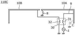
图35是第18实施方式所涉及的天线装置118A的电路图。该天线装置118A在金属壳体的侧面部构成无供电辐射元件10B。耦合电路30的第2耦合元件32与无供电辐射元件10B连接。其他的结构与第1实施方式中图4所示的电路相同。FIG. 35 is a circuit diagram of an
根据天线装置118A的构造,能够将无供电辐射元件10B从辐射元件10分离,能够以通过耦合电路30以及无供电辐射元件10B而追加的谐振频率得到良好的辐射特性。进一步地,不会以该谐振频率以外的频率使辐射元件10所具有的辐射特性劣化。According to the structure of the
图36是第18实施方式所涉及的其它的天线装置1 18B的电路图。该天线装置1 18B在金属壳体的侧面部构成无供电辐射元件10B。无供电辐射元件10B的端部经由电感器8而与电路基板等的接地连接(接地)。该无供电辐射元件10B作用为1/2波长谐振型的天线。FIG. 36 is a circuit diagram of another
根据天线装置118B的构造,通过金属壳体的侧面部的前端接地,能够抑制基于周边环境的变化的天线特性的变动。此外,即便在金属壳体的侧面部的前端的端部存在夹着狭缝而接地的其他金属壳体的侧面部的情况下,通过金属壳体的侧面部的前端接地,从而电场最大位置从无供电辐射元件10B的前端向中央方向移动,因此能够以通过耦合电路30而追加的谐振频率得到良好的辐射特性。进一步地,通过电感器8的电感,能够容易地调整谐振频率。According to the structure of the
图37是第18实施方式所涉及的又一天线装置118C的电路图。该天线装置118C从金属壳体的端面部到侧面部构成供电辐射元件10A。同样地,从金属壳体的端面部到侧面部构成无供电辐射元件10B。这样无供电辐射元件10B的主要部分也可以处于金属壳体的端面部。此外,无供电辐射元件10B也可以接近于供电辐射元件10A的接地端。通过该构造,由于供电辐射元件10A的电场最大位置从接地端向中央方向移动,因此能够抑制供电辐射元件10A与无供电辐射元件10B的不必要的干扰。FIG. 37 is a circuit diagram of still another
《第19实施方式》"19th Embodiment"
图38是第19实施方式的天线装置119的主要部分的俯视图。FIG. 38 is a plan view of the main part of the
电子设备的金属壳体具备作为金属壳体端部的辐射元件10。与第1实施方式中图2所示的天线装置101相比,供电线路9相对于辐射元件10的连接位置以及非辐射性谐振电路20的位置不同。The metal casing of the electronic device includes the radiating
在本实施方式中,在电路基板6的俯视情况下,在辐射元件10的左侧的侧面部13连接供电线路9。伴随于此,在耦合电路30的右侧配置非辐射性谐振电路20。这些的位置关系与图2所示的例子相比,左右相反(左右对称关系)。其他的结构如第1实施方式中所示。In the present embodiment, the
图39是本实施方式的耦合电路30的立体图。该耦合电路30的外形通过双点划线来表示。在耦合电路30的外表面,形成供电电路连接端子PF、辐射元件连接端子PA、接地端子PG以及非辐射性谐振电路连接端子PS。该耦合电路30是与第1实施方式中图1所示的耦合电路30实质相同的元件。其中,第2面MS2是安装面,该面与电路基板对置。对与安装面(第2面)MS2相反的一侧的面即顶面(第1面)赋予方向识别标记DDM。因此,与图1所示的耦合电路30相比,俯视情况下的各端子的位置不同。在图1所示的耦合电路30中,俯视情况下,从辐射元件连接端子PA起向顺时针旋转地,依次形成接地端子PG、供电电路连接端子PF以及非辐射性谐振电路连接端子PS。在第19实施方式中,如图39所示,从辐射元件连接端子PA向逆时针旋转地,依次形成接地端子PG、供电电路连接端子PF以及非辐射性谐振电路连接端子PS。FIG. 39 is a perspective view of the
如上所述,通过在第1面MS1、第2面MS2这两面,形成第1耦合元件的第1端、第2端以及第2线圈的第1端、第2端,从而第1面、第2面均能够设为安装面。因此,能够将耦合电路30的第1面MS1、第2面MS2的任意一个选择性地作为安装面而安装于电路基板,以使得在适合于形成于该耦合电路30的第1耦合元件以及第2耦合元件的连接对象的电路或元件的位置的位置配置各端子。As described above, by forming the first and second ends of the first coupling element and the first and second ends of the second coil on both the first and second surfaces MS1 and MS2, the first and second Both surfaces can be used as mounting surfaces. Therefore, any one of the first surface MS1 and the second surface MS2 of the
另外,在图8、图39所示的例子中,表示了将形成于第1面MS1的4个端子与形成于第2面MS2的4个端子连接的层间连接导体形成在层叠体的端面的例子,但也可以在层叠体的内部形成多个通孔导体,经由这些通孔导体,将形成于第1面MS1的4个端子与形成于第2面MS2的4个端子连接。In addition, in the examples shown in FIGS. 8 and 39 , the interlayer connection conductors that connect the four terminals formed on the first surface MS1 and the four terminals formed on the second surface MS2 are formed on the end surfaces of the laminate. However, a plurality of via-hole conductors may be formed inside the laminate, and the four terminals formed on the first surface MS1 and the four terminals formed on the second surface MS2 may be connected via these via-hole conductors.
此外,也可以形成上述通孔导体,并且在耦合电路30的安装面形成LGA(Land GridArray)型的端子。In addition, the above-mentioned through-hole conductors may be formed, and LGA (Land Grid Array) type terminals may be formed on the mounting surface of the
图40是表示本实施方式的另一耦合电路30的结构的图,是表示形成于耦合电路30的各层的导体图案的分解俯视图。FIG. 40 is a diagram showing the configuration of another
如图40所示,在绝缘基材S11形成第1导体图案L11,在绝缘基材S12形成第2导体图案L12,在绝缘基材S21形成第3导体图案L21,在绝缘基材S22形成第4导体图案L22。绝缘基材S11、S12、S21、S22被层叠,以使得这些线圈导体图案从接近于安装面的层起依次配置第1导体图案L11、第2导体图案L12、第3导体图案L21、第4导体图案L22。As shown in FIG. 40 , the first conductor pattern L11 is formed on the insulating substrate S11, the second conductor pattern L12 is formed on the insulating substrate S12, the third conductor pattern L21 is formed on the insulating substrate S21, and the fourth conductor pattern L21 is formed on the insulating substrate S22. Conductor pattern L22. The insulating base materials S11 , S12 , S21 , and S22 are laminated so that the first conductor pattern L11 , the second conductor pattern L12 , the third conductor pattern L21 , and the fourth conductor are arranged in this order from the layer close to the mounting surface. Pattern L22.
第1导体图案L11的第1端与辐射元件连接端子PA连接,第2端经由层间连接导体V1而与第2导体图案L12的第1端连接。第2导体图案L12的第2端与供电电路连接端子PF连接。此外,第3导体图案L21的第1端与非辐射性谐振电路连接端子PS连接,第3导体图案L21的第2端经由层间连接导体V2而与第4导体图案L22的第1端连接。第4导体图案L22的第2端与接地端子PG连接。The first end of the first conductor pattern L11 is connected to the radiation element connection terminal PA, and the second end is connected to the first end of the second conductor pattern L12 via the interlayer connection conductor V1. The second end of the second conductor pattern L12 is connected to the power supply circuit connection terminal PF. In addition, the first end of the third conductor pattern L21 is connected to the non-radiative resonance circuit connection terminal PS, and the second end of the third conductor pattern L21 is connected to the first end of the fourth conductor pattern L22 via the interlayer connection conductor V2. The second end of the fourth conductor pattern L22 is connected to the ground terminal PG.
图40所示的各层的导体图案处于与图9所示的导体图案左右对称的关系。因此,具备这些导体图案的耦合电路在俯视情况下,从辐射元件连接端子PA向逆时针旋转地,依次形成接地端子PG、供电电路连接端子PF以及非辐射性谐振电路连接端子PS。The conductor pattern of each layer shown in FIG. 40 is in a bilaterally symmetrical relationship with the conductor pattern shown in FIG. 9 . Therefore, the coupling circuit provided with these conductor patterns forms the ground terminal PG, the power supply circuit connection terminal PF, and the non-radiative resonance circuit connection terminal PS in this order from the radiation element connection terminal PA to the counterclockwise direction in plan view.
如本例这样,耦合电路30也可以在适合于形成于其的第1耦合元件以及第2耦合元件的连接对象的电路或元件的位置的位置配置各端子。As in this example, the
《第20实施方式》"Twentieth Embodiment"
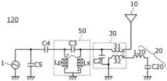
在第20实施方式中,表示还具备移相器的天线装置。In the twentieth embodiment, an antenna apparatus further including a phase shifter is shown.
图41是供电电路1所连接的第20实施方式所涉及的天线装置120的电路图。该天线装置120在供电电路1与耦合电路30的第1耦合元件31之间连接移相器50。该移相器50是移相量根据频率而变化(具有频率依赖性)的移相器。移相器50具备相互耦合的第1耦合元件Lp、第2线圈Ls以及电容器C3。FIG. 41 is a circuit diagram of the
另外,在本例中,在供电电路1与移相器50之间连接阻抗匹配用的电容器C4、C5。In addition, in this example, capacitors C4 and C5 for impedance matching are connected between the
耦合电路30、辐射元件10、非辐射性谐振电路20的结构与第1实施方式中所示的相同。The configurations of the
图42是将上述移相器50分为理想变压器IT与寄生电感成分(串联寄生电感成分La、Lc、并联寄生电感成分Lb)来表示的等效电路图。42 is an equivalent circuit diagram showing the above-described
图41所示的第1线圈Lp与第2线圈Ls的耦合系数比一般的高频变压器小,伴随于此,串联寄生电感成分Lc较大。但是,通过电容器C3的电容也较大,能够确保阻抗匹配。此外,通过电容器C3的电容较大,高频带的信号与基于第1线圈Lp和第2线圈Ls的变压器相比,将电容器C3分流的比例较大,基于变压器的移相作用较小。另一方面,低频带的将电容器C3分流的量相对较小,基于变压器的移相作用较大。由此,耦合系数被规定,以使得相对于低频带的信号的移相量几乎为180°,相对于高频带的信号的移相量几乎为90°。The coupling coefficient between the first coil Lp and the second coil Ls shown in FIG. 41 is smaller than that of a general high-frequency transformer, and accordingly, the series parasitic inductance component Lc is large. However, since the capacitance of the capacitor C3 is also large, impedance matching can be ensured. In addition, since the capacitance of the capacitor C3 is large, the ratio of the shunt of the capacitor C3 is large compared to the transformer based on the first coil Lp and the second coil Ls, and the phase shift effect by the transformer is small. On the other hand, the amount of shunting capacitor C3 in the low frequency band is relatively small, and the phase shifting effect based on the transformer is large. Accordingly, the coupling coefficient is defined so that the phase shift amount with respect to the low-band signal is almost 180°, and the phase-shift amount with respect to the high-band signal is almost 90°.
图43是表示移相器50的移相量的频率特性的图。在本例中,在低频带(从700MHz到900MHz频带),移相量几乎为180°,在高频带(从1.7GHz到2.7GHz频带),移相量几乎为90°。FIG. 43 is a graph showing the frequency characteristic of the phase shift amount of the
接下来,表示基于设置了上述耦合电路30以及移相器50的作用效果。图44的(A)是不具备上述移相器50的第1实施方式中所示的天线装置的电路图,图44的(B)是在史密斯圆图上表示从供电电路1观察该天线装置的阻抗的阻抗轨迹。Next, the effect of providing the
图45的(A)是追加了上述移相器50的天线装置的电路图,图45的(B)是在史密斯圆图上表示从供电电路1观察该天线装置的阻抗的阻抗轨迹。该天线装置是在图41所示的电路中不具备电容器C5的电路。45(A) is a circuit diagram of the antenna device to which the
图46的(A)是具备阻抗匹配用电容器C5的天线装置的电路图(与图41所示的相同),图46的(B)是在史密斯圆图上表示从供电电路1观察该天线装置的阻抗的阻抗轨迹。(A) of FIG. 46 is a circuit diagram of an antenna device including an impedance matching capacitor C5 (the same as that shown in FIG. 41 ), and (B) of FIG. 46 shows the antenna device viewed from the
在图44的(B)中,轨迹T0是未设置耦合电路30以及非辐射性谐振电路20的比较例的天线装置的阻抗轨迹,轨迹T1是图44的(A)所示的天线装置的阻抗轨迹。均为从1.7GHz到2.7GHz扫描的结果。根据该图44的(B)可知,通过具备耦合电路30以及非辐射性谐振电路20,如已经所述那样,在天线的频率特性产生极点(圆图上为小环状),此外,伴随于此,谐振频带向圆图的中心方向移动。其中,可知更高频率区域未处于圆图的周边部,高频率区域难以匹配。In FIG. 44(B), the trace T0 is the impedance trace of the antenna apparatus of the comparative example in which the
在图45的(B)中,轨迹T2是具备移相器50、耦合电路30以及非辐射性谐振电路20的天线装置的阻抗轨迹,轨迹T1与图44的(A)所示的轨迹T1相同。均为从1.7GHz到2.7GHz扫描的结果。根据该图45的(B)可知,通过具备移相器50,在低频带大约提前180°相位,在高频带大约提前90°相位。由此,高频率区域也向圆图的中心方向移动。In FIG. 45(B), the trace T2 is the impedance trace of the antenna device including the
在图46的(B)中,轨迹T3是图46的(A)所示的天线装置的阻抗轨迹,是从1.7GHz到2.7GHz扫描的结果。与图45的(B)所示的轨迹T2相比可知,通过分流连接的电容器C5的作用,高频率区域顺时针旋转。由此,在整个频率区域更加匹配。In (B) of FIG. 46 , the trace T3 is the impedance trace of the antenna device shown in (A) of FIG. 46 , and is the result of scanning from 1.7 GHz to 2.7 GHz. Compared with the trace T2 shown in (B) of FIG. 45 , it can be seen that the high-frequency region rotates clockwise by the action of the capacitor C5 connected by the shunt. Thereby, more matching is achieved over the entire frequency region.
图47是表示图44的(A)、图46的(A)所示的各天线装置以及比较例的天线装置的反射损耗的频率特性的图。在图47中,反射损耗特性RL1是不具备耦合电路30以及非辐射性谐振电路20的比较例的天线装置的反射损耗的特性,反射损耗特性RL2是图44的(A)所示的天线装置的反射损耗的特性,反射损耗特性RL3是图46的(A)所示的天线装置的反射损耗的特性。图47中的反射损耗特性RL1、RL2与图6所示的相同。若对反射损耗特性RL2与RL3进行比较,可知在整个区域,反射损耗较小,使用相同的辐射元件,也能够将高频带扩展到例如从1.4GHz到2.6GHz的宽频带。FIG. 47 is a graph showing frequency characteristics of the return loss of each of the antenna devices shown in FIG. 44(A) and FIG. 46(A) and the antenna device of the comparative example. In FIG. 47 , the return loss characteristic RL1 is the return loss characteristic of the antenna device of the comparative example which does not include the
图48是移相器50的外观立体图,图49是移相器50的各层的俯视图。此外,图50是移相器50的剖视图。FIG. 48 is an external perspective view of the
基材S1的上表面相当于层叠体100的安装面(下表面)。在基材S1形成作为第1端口P1的端子T1、作为第2端口P2的端子T2、接地端子G、空闲端子NC。The upper surface of the base material S1 corresponds to the mounting surface (lower surface) of the
层叠体100的各基材层可以是由LTCC等构成的非磁性陶瓷层叠体,也可以是由聚酰亚胺或液晶聚合物等树脂材料构成的树脂层叠体。这样,通过基材层是非磁性体(由于不是磁性铁氧体),从而即便在超过几百MHz的高频带也能够用作为给定电感、给定耦合系数的变压器以及移相器。Each base material layer of the laminate 100 may be a non-magnetic ceramic laminate made of LTCC or the like, or a resin laminate made of a resin material such as polyimide or liquid crystal polymer. In this way, since the base material layer is a non-magnetic material (because it is not a magnetic ferrite), it can be used as a transformer and a phase shifter with a given inductance and a given coupling coefficient even in a high frequency band exceeding several hundreds of MHz.
上述导体图案以及层间连接导体由以Ag或Cu为主成分的电阻率较小的导体材料构成。若基材层是陶瓷,则例如通过以Ag或Cu为主成分的导电性膏的丝网印刷以及烧成而形成。此外,若基材层是树脂,则例如通过Al箔或Cu箔等金属箔利用蚀刻等而被图案化而形成。The conductor pattern and the interlayer connection conductor are formed of a conductor material with a low resistivity mainly composed of Ag or Cu. When the base material layer is a ceramic, it is formed by, for example, screen printing and firing of a conductive paste containing Ag or Cu as a main component. In addition, when the base material layer is resin, it is formed by patterning, for example, metal foil such as Al foil or Cu foil by etching or the like.
移相器50具备多个绝缘性的基材S1~S9。在基材S1~S9形成各种导体图案。在“各种导体图案”中,不仅包含形成于基材的表面的导体图案,也包含层间连接导体。层间连接导体不仅包含通孔导体,也包含形成于层叠体的端面的端面电极。The
基材S1的上表面相当于层叠体的安装面(下表面)。在基材S1形成作为第1端口P1的端子T1、作为第2端口P2的端子T2、接地端子G、空闲端子NC。The upper surface of the base material S1 corresponds to the mounting surface (lower surface) of the laminate. A terminal T1 serving as a first port P1, a terminal T2 serving as a second port P2, a ground terminal G, and a free terminal NC are formed on the substrate S1.
在基材S5、S4分别形成导体L1A1、L1A2。在基材S3形成导体L1A3、L1B1。在基材S2形成导体L1B2、L1C。Conductors L1A1 and L1A2 are formed on the base materials S5 and S4, respectively. Conductors L1A3 and L1B1 are formed on the base material S3. Conductors L1B2 and L1C are formed on the base material S2.
导体L1A1的第1端与第1端口的端子T1连接。导体L1A1的第2端经由层间连接导体V11而与导体L1A2的第1端连接。导体L1A2的第2端经由层间连接导体V12而与导体L1A3的第1端连接。导体L1A3的第2端与导体L1B1的第1端连接。导体L1A3的第2端以及导体L1B1的第1端经由层间连接导体V13而与导体L1B2的第1端连接。导体L1B1的第2端经由层间连接导体V14而与导体L1B2的第2端连接。导体L1B2的第2端与导体L1C的第1端连接。导体L1C的第2端与接地端子G连接。The first end of the conductor L1A1 is connected to the terminal T1 of the first port. The second end of the conductor L1A1 is connected to the first end of the conductor L1A2 via the interlayer connecting conductor V11. The second end of the conductor L1A2 is connected to the first end of the conductor L1A3 via the interlayer connecting conductor V12. The second end of the conductor L1A3 is connected to the first end of the conductor L1B1. The second end of the conductor L1A3 and the first end of the conductor L1B1 are connected to the first end of the conductor L1B2 via the interlayer connecting conductor V13. The second end of the conductor L1B1 is connected to the second end of the conductor L1B2 via the interlayer connecting conductor V14. The second end of the conductor L1B2 is connected to the first end of the conductor L1C. The second end of the conductor L1C is connected to the ground terminal G.
在基材S6、S7分别形成导体L2A1、L2A2。在基材S8形成导体L2A3、L2B1。在基材S9形成导体L2B2、L2C。Conductors L2A1 and L2A2 are formed on the base materials S6 and S7, respectively. Conductors L2A3 and L2B1 are formed on the base material S8. Conductors L2B2 and L2C are formed on the base material S9.
导体L2A1的第1端与第2端口的端子T2连接。导体L2A1的第2端经由层间连接导体V21而与导体L2A2的第1端连接。导体L2A2的第2端经由层间连接导体V22而与导体L2A3的第1端连接。导体L2A3的第2端与导体L2B1的第1端连接。导体L2A3的第2端以及导体L2B1的第1端经由层间连接导体V23而与导体L2B2的第1端连接。导体L2B1的第2端经由层间连接导体V24而与导体L2B2的第2端连接。导体L2B2的第2端与导体L2C的第1端连接。导体L2C的第2端与接地端子G连接。The first end of the conductor L2A1 is connected to the terminal T2 of the second port. The second end of the conductor L2A1 is connected to the first end of the conductor L2A2 via the interlayer connecting conductor V21. The second end of the conductor L2A2 is connected to the first end of the conductor L2A3 via the interlayer connecting conductor V22. The second end of the conductor L2A3 is connected to the first end of the conductor L2B1. The second end of the conductor L2A3 and the first end of the conductor L2B1 are connected to the first end of the conductor L2B2 via the interlayer connection conductor V23. The second end of the conductor L2B1 is connected to the second end of the conductor L2B2 via the interlayer connecting conductor V24. The second end of the conductor L2B2 is connected to the first end of the conductor L2C. The second end of the conductor L2C is connected to the ground terminal G.
由上述导体L1A1、L1A2、L1A3、L1B1、L1B2、L1C以及层间连接导体V11、V12、V13、V14构成第1线圈Lp。此外,由上述导体L2A1、L2A2、L2A3、L2B1、L2B2、L2C以及层间连接导体V21、V22、V23、V24构成第2线圈Ls。第1线圈Lp、第2线圈Ls都为矩形螺旋状的线圈。The first coil Lp is constituted by the conductors L1A1 , L1A2 , L1A3 , L1B1 , L1B2 , and L1C and the interlayer connection conductors V11 , V12 , V13 , and V14 . Further, the second coil Ls is constituted by the conductors L2A1 , L2A2 , L2A3 , L2B1 , L2B2 , and L2C and the interlayer connection conductors V21 , V22 , V23 , and V24 . Both the first coil Lp and the second coil Ls are rectangular helical coils.
《第21实施方式》"Twenty-first Embodiment"
在第21实施方式中,表示与第1实施方式中所示的辐射元件不同构造的辐射元件。In the twenty-first embodiment, a radiation element having a structure different from that shown in the first embodiment is shown.
图51是表示电子设备的金属壳体的一部分的俯视图。电子设备的金属壳体具备作为金属壳体端部的辐射元件10和金属壳体主要部分40。在第1实施方式中,表示了将俯视情况下具有3边的金属壳体端部用作为辐射元件10的例子,但也可以如图51所示,辐射元件10由平板状的金属壳体端部构成。FIG. 51 is a plan view showing a part of a metal case of an electronic device. The metal case of the electronic device includes a radiating
图52的(A)、(B)是表示分别不同的电子设备的金属壳体的一部分的立体图。在图52的(A)所示的例子中,作为金属壳体端部的辐射元件10具有与X-Y面平行的一个面和与Y-Z面平行的一个面。在图52的(B)所示的例子中,作为金属壳体端部的辐射元件10具有与X-Y面平行的一个面、与Y-Z面平行的一个面、与X-Z面平行的两个面。(A) and (B) of FIG. 52 are perspective views showing a part of metal casings of different electronic devices. In the example shown in FIG. 52(A) , the
如图52的(A)、(B)所示,金属壳体端部的形状能够采用各种形态。As shown in (A) and (B) of FIG. 52 , various forms can be adopted for the shape of the end portion of the metal case.
《其他实施方式》"Other Embodiments"
在以上所示的实施方式中,表示了将金属壳体端部利用为辐射元件的例子,但辐射元件也可以是一部分或者全部形成于电路基板等的导体图案。此外,也可以是与壳体不同的部件。In the above-described embodiment, the example in which the end of the metal case is used as the radiating element is shown, but the radiating element may be a part or all of a conductor pattern formed on a circuit board or the like. In addition, it may be a different member from the casing.
此外,在图4所示的例子中,图示了在辐射元件10的一端与接地之间产生寄生电容,但也可以通过在该位置积极地设置高频带且低阻抗的电容,来使辐射元件10作用为PIFA。此外,也可以将上述电容产生的位置与接地连接,来构成PIFA。In addition, in the example shown in FIG. 4, the parasitic capacitance is generated between one end of the
非辐射性谐振电路20并不局限于线状导体图案在中途折回的形状,也可以单向地延伸。此外,可以折弯为L字状,也可以弯曲。进一步地,也可以具有分支为多个的导体图案。由此,产生多个极点。The non-radiative
此外,非辐射性谐振电路20也可以将线状导体图案的前端与接地连接,构成与短路短截线类似的电路。In addition, the
在以上所示的例子中,主要说明了利用非辐射性谐振电路20的基本波谐振的例子,但也可以利用非辐射性谐振电路20的2倍波谐振(2阶谐振)、3倍波谐振(3阶谐振)、3/2倍波谐振等的高谐波谐振。此外,也可以利用基本波谐振和高谐波谐振这两个,还可以利用多个高谐波谐振。In the example shown above, the example using the fundamental wave resonance of the
此外,针对辐射元件10也同样地,也可以利用2倍波谐振(2阶谐振)、3倍波谐振(3阶谐振)、3/2倍波谐振等的高谐波谐振。此外,也可以利用基本波谐振和高谐波谐振这两个,还可以利用多个高谐波谐振。In addition, similarly to the
在以上所示的实施方式中,表示了所谓的智能手机或者与其相同形状的电子设备,但也能够同样应用于功能手机等移动电话、智能手表或智能眼镜等可穿戴终端、笔记本PC、平板终端、照相机、游戏机、玩具等各种电子设备。In the above-described embodiments, a so-called smartphone or an electronic device having the same shape is shown, but the same can be applied to mobile phones such as feature phones, wearable terminals such as smart watches and smart glasses, notebook PCs, and tablet terminals. , cameras, game consoles, toys and other electronic equipment.
最后,上述的实施方式的说明在全部的方面为示例,并不是限制性的。对于本领域的技术人员来说能够适当地进行变形以及变更。本发明的范围并不由上述的实施方式表示,而由权利要求书来表示。进一步地,在本发明的范围中,包含从与权利要求书等同的范围内的实施方式的变更。Finally, the description of the above-mentioned embodiment is an example in all respects, and it is not restrictive. Deformations and changes can be appropriately made by those skilled in the art. The scope of the present invention is shown not by the above-described embodiments but by the claims. Furthermore, within the scope of the present invention, modifications of the embodiments within the scope equivalent to the scope of the claims are included.
Claims (20)
Translated fromChinesePriority Applications (1)
| Application Number | Priority Date | Filing Date | Title |
|---|---|---|---|
| CN202010860163.2ACN112002993B (en) | 2016-11-29 | 2017-11-29 | Antenna devices and electronic equipment |
Applications Claiming Priority (13)
| Application Number | Priority Date | Filing Date | Title |
|---|---|---|---|
| JP2016231024 | 2016-11-29 | ||
| JP2016-231024 | 2016-11-29 | ||
| JP2016255729 | 2016-12-28 | ||
| JP2016-255729 | 2016-12-28 | ||
| JP2017082043 | 2017-04-18 | ||
| JP2017-082043 | 2017-04-18 | ||
| JP2017-104650 | 2017-05-26 | ||
| JP2017104650 | 2017-05-26 | ||
| JP2017158218 | 2017-08-18 | ||
| JP2017-158218 | 2017-08-18 | ||
| CN201780055966.7ACN109716583B (en) | 2016-11-29 | 2017-11-29 | Antenna devices and electronic equipment |
| PCT/JP2017/042706WO2018101284A1 (en) | 2016-11-29 | 2017-11-29 | Antenna device and electronic instrument |
| CN202010860163.2ACN112002993B (en) | 2016-11-29 | 2017-11-29 | Antenna devices and electronic equipment |
Related Parent Applications (1)
| Application Number | Title | Priority Date | Filing Date |
|---|---|---|---|
| CN201780055966.7ADivisionCN109716583B (en) | 2016-11-29 | 2017-11-29 | Antenna devices and electronic equipment |
Publications (2)
| Publication Number | Publication Date |
|---|---|
| CN112002993Atrue CN112002993A (en) | 2020-11-27 |
| CN112002993B CN112002993B (en) | 2023-09-19 |
Family
ID=62242884
Family Applications (5)
| Application Number | Title | Priority Date | Filing Date |
|---|---|---|---|
| CN202010860140.1AActiveCN112002992B (en) | 2016-11-29 | 2017-11-29 | Antenna devices and electronic equipment |
| CN202010860163.2AActiveCN112002993B (en) | 2016-11-29 | 2017-11-29 | Antenna devices and electronic equipment |
| CN201780055966.7AActiveCN109716583B (en) | 2016-11-29 | 2017-11-29 | Antenna devices and electronic equipment |
| CN201721633688.2UActiveCN207800911U (en) | 2016-11-29 | 2017-11-29 | Antenna device and electronic apparatus |
| CN201821287632.0UActiveCN208797170U (en) | 2016-11-29 | 2017-11-29 | Antenna device |
Family Applications Before (1)
| Application Number | Title | Priority Date | Filing Date |
|---|---|---|---|
| CN202010860140.1AActiveCN112002992B (en) | 2016-11-29 | 2017-11-29 | Antenna devices and electronic equipment |
Family Applications After (3)
| Application Number | Title | Priority Date | Filing Date |
|---|---|---|---|
| CN201780055966.7AActiveCN109716583B (en) | 2016-11-29 | 2017-11-29 | Antenna devices and electronic equipment |
| CN201721633688.2UActiveCN207800911U (en) | 2016-11-29 | 2017-11-29 | Antenna device and electronic apparatus |
| CN201821287632.0UActiveCN208797170U (en) | 2016-11-29 | 2017-11-29 | Antenna device |
Country Status (5)
| Country | Link |
|---|---|
| US (2) | US11128046B2 (en) |
| JP (1) | JP6614363B2 (en) |
| CN (5) | CN112002992B (en) |
| DE (1) | DE112017004788T5 (en) |
| WO (1) | WO2018101284A1 (en) |
Cited By (1)
| Publication number | Priority date | Publication date | Assignee | Title |
|---|---|---|---|---|
| US12155115B2 (en) | 2021-09-23 | 2024-11-26 | Samsung Electronics Co., Ltd. | Electronic device including antenna assembly |
Families Citing this family (19)
| Publication number | Priority date | Publication date | Assignee | Title |
|---|---|---|---|---|
| WO2019208297A1 (en)* | 2018-04-25 | 2019-10-31 | 株式会社村田製作所 | Antenna coupling element, antenna device, and communication terminal device |
| CN212676477U (en)* | 2018-04-25 | 2021-03-09 | 株式会社村田制作所 | Antenna device and communication terminal device |
| CN214280210U (en)* | 2018-06-25 | 2021-09-24 | 株式会社村田制作所 | Antenna device and electronic apparatus |
| CN109546310B (en)* | 2018-12-12 | 2021-01-08 | 维沃移动通信有限公司 | Antenna structure and communication terminal |
| JP6835299B2 (en)* | 2018-12-28 | 2021-02-24 | 株式会社村田製作所 | Antenna device |
| DE102019204163B3 (en)* | 2019-03-26 | 2020-10-01 | Fraunhofer-Gesellschaft zur Förderung der angewandten Forschung e.V. | Generation of a tuning signal for tuning a magnetic antenna |
| US12160055B2 (en)* | 2019-06-25 | 2024-12-03 | Kyocera Corporation | Antenna, wireless communication module, and wireless communication device |
| JP6897900B1 (en)* | 2019-08-27 | 2021-07-07 | 株式会社村田製作所 | Antenna device and electronic equipment |
| JP6892044B1 (en)* | 2019-09-19 | 2021-06-18 | 株式会社村田製作所 | Antenna device and electronic equipment |
| JP7209314B2 (en)* | 2019-11-13 | 2023-01-20 | 国立大学法人埼玉大学 | Antenna module and communication device equipped with it |
| CN112838371B (en)* | 2019-11-22 | 2025-04-15 | 中兴通讯股份有限公司 | Antenna multiplexing system and terminal |
| CN113258268B (en)* | 2021-04-12 | 2022-11-01 | 荣耀终端有限公司 | Antenna device and electronic apparatus |
| CN115411501B (en)* | 2021-05-26 | 2024-12-31 | Oppo广东移动通信有限公司 | Antenna assembly and electronic equipment |
| JP7568122B2 (en) | 2021-09-03 | 2024-10-16 | 株式会社村田製作所 | Antenna device and communication terminal device |
| CN114142228A (en)* | 2021-12-31 | 2022-03-04 | 维沃移动通信有限公司 | Antenna structure and electronic device |
| TWI823424B (en)* | 2022-06-14 | 2023-11-21 | 廣達電腦股份有限公司 | Wearable device |
| JPWO2024247363A1 (en)* | 2023-05-29 | 2024-12-05 | ||
| US20240405434A1 (en)* | 2023-06-05 | 2024-12-05 | Analog Devices International Unlimited Company | Apparatus and methods for inverted-l and inverted-f antennas |
| WO2025022716A1 (en)* | 2023-07-26 | 2025-01-30 | 株式会社村田製作所 | Antenna device and electronic apparatus |
Citations (23)
| Publication number | Priority date | Publication date | Assignee | Title |
|---|---|---|---|---|
| CN1341978A (en)* | 2000-08-24 | 2002-03-27 | 株式会社村田制作所 | Antenna device and radio equipment containing said antenna |
| JP2002319811A (en)* | 2001-04-19 | 2002-10-31 | Murata Mfg Co Ltd | Plural resonance antenna |
| CN1650475A (en)* | 2002-10-15 | 2005-08-03 | 株式会社日立制作所 | Small multi-mode antenna and high-frequency module using it |
| JP2009135633A (en)* | 2007-11-29 | 2009-06-18 | Furukawa Electric Co Ltd:The | antenna |
| JP2010016298A (en)* | 2008-07-07 | 2010-01-21 | Kurita Water Ind Ltd | Method of forming thin metal oxide film |
| JP2010258924A (en)* | 2009-04-28 | 2010-11-11 | Murata Mfg Co Ltd | Antenna and radio communication device |
| US20110128200A1 (en)* | 2009-11-27 | 2011-06-02 | Fujitsu Limited | Antenna and radio communication apparatus |
| JPWO2010016298A1 (en)* | 2008-08-05 | 2012-01-19 | 株式会社村田製作所 | Antenna and wireless communication device |
| JP2012109809A (en)* | 2010-11-17 | 2012-06-07 | Panasonic Corp | Antenna device |
| JP2012191596A (en)* | 2011-02-23 | 2012-10-04 | Murata Mfg Co Ltd | Impedance conversion device, antenna apparatus and communication terminal apparatus |
| WO2012153690A1 (en)* | 2011-05-09 | 2012-11-15 | 株式会社村田製作所 | Coupling degree adjustment circuit, antenna and communication terminal |
| CN202997046U (en)* | 2012-03-28 | 2013-06-12 | 株式会社村田制作所 | Multiband antenna apparatus |
| WO2014034587A1 (en)* | 2012-08-28 | 2014-03-06 | 株式会社村田製作所 | Antenna device, and communication terminal device |
| JP2014053808A (en)* | 2012-09-07 | 2014-03-20 | Murata Mfg Co Ltd | Coupling degree adjustment element, antenna device, and radio communication device |
| WO2014155875A1 (en)* | 2013-03-27 | 2014-10-02 | 株式会社コスモライフ | Water server |
| US20140361948A1 (en)* | 2013-06-06 | 2014-12-11 | Sony Corporation | Antenna system |
| US20150145744A1 (en)* | 2013-11-28 | 2015-05-28 | Asustek Computer Inc. | Tunable antenna |
| WO2015178204A1 (en)* | 2014-05-19 | 2015-11-26 | 株式会社村田製作所 | Antenna matching circuit, antenna matching module, antenna device, and radio communication apparatus |
| CN105762517A (en)* | 2012-07-20 | 2016-07-13 | 旭硝子株式会社 | Antenna device and wireless apparatus including same |
| WO2016114182A1 (en)* | 2015-01-16 | 2016-07-21 | 株式会社村田製作所 | Antenna matching circuit, antenna device, and communication terminal device |
| WO2016143724A1 (en)* | 2015-03-12 | 2016-09-15 | 株式会社村田製作所 | Antenna device and communication terminal apparatus |
| WO2016152603A1 (en)* | 2015-03-25 | 2016-09-29 | 株式会社村田製作所 | Phase shifter, impedance matching circuit, multiplexer/demultiplexer and communication terminal device |
| WO2016186091A1 (en)* | 2015-05-19 | 2016-11-24 | 株式会社村田製作所 | Antenna device and electronic apparatus |
Family Cites Families (15)
| Publication number | Priority date | Publication date | Assignee | Title |
|---|---|---|---|---|
| JPS427857Y1 (en)* | 1964-12-29 | 1967-04-19 | ||
| JPS54183246U (en)* | 1978-06-15 | 1979-12-26 | ||
| JP2003110353A (en)* | 2001-09-27 | 2003-04-11 | Mitsubishi Electric Corp | Dual-polarized array antenna |
| US9607188B2 (en)* | 2014-09-29 | 2017-03-28 | Rfmicron, Inc. | Radio frequency identification (RFID) tag(s) and sensor(s) |
| CN101299485B (en)* | 2007-05-01 | 2012-02-01 | 佛山市顺德区顺达电脑厂有限公司 | Coupled antenna with multi-frequency band resonance segment antenna pattern |
| JP5306158B2 (en)* | 2009-12-07 | 2013-10-02 | アルプス電気株式会社 | Antenna device |
| JP5234084B2 (en)* | 2010-11-05 | 2013-07-10 | 株式会社村田製作所 | Antenna device and communication terminal device |
| JP2012235402A (en)* | 2011-05-09 | 2012-11-29 | Murata Mfg Co Ltd | Impedance matching circuit, antenna device, and communication terminal apparatus |
| GB201111120D0 (en)* | 2011-06-29 | 2011-08-10 | Roke Manor Research | Reduced Q low frequency antenna |
| EP2733787B1 (en)* | 2012-06-28 | 2017-09-06 | Murata Manufacturing Co., Ltd. | Antenna device and communication terminal device |
| WO2014155873A1 (en)* | 2013-03-29 | 2014-10-02 | 株式会社村田製作所 | Laminated coil component and matching circuit |
| US9711841B2 (en)* | 2013-09-20 | 2017-07-18 | Sony Corporation | Apparatus for tuning multi-band frame antenna |
| US10622702B2 (en)* | 2014-12-26 | 2020-04-14 | Byd Company Limited | Mobile terminal and antenna of mobile terminal |
| CN105789882B (en)* | 2014-12-26 | 2019-05-17 | 比亚迪股份有限公司 | The antenna of mobile terminal and mobile terminal |
| CN104901000B (en)* | 2015-05-14 | 2018-07-06 | 广东欧珀移动通信有限公司 | A kind of couple feed reconfigurable antenna and manufacturing method |
- 2017
- 2017-11-29CNCN202010860140.1Apatent/CN112002992B/enactiveActive
- 2017-11-29CNCN202010860163.2Apatent/CN112002993B/enactiveActive
- 2017-11-29DEDE112017004788.9Tpatent/DE112017004788T5/enactivePending
- 2017-11-29CNCN201780055966.7Apatent/CN109716583B/enactiveActive
- 2017-11-29JPJP2018554170Apatent/JP6614363B2/enactiveActive
- 2017-11-29CNCN201721633688.2Upatent/CN207800911U/enactiveActive
- 2017-11-29WOPCT/JP2017/042706patent/WO2018101284A1/ennot_activeCeased
- 2017-11-29CNCN201821287632.0Upatent/CN208797170U/enactiveActive
- 2019
- 2019-03-15USUS16/354,222patent/US11128046B2/enactiveActive
- 2021
- 2021-08-11USUS17/399,166patent/US12218438B2/enactiveActive
Patent Citations (28)
| Publication number | Priority date | Publication date | Assignee | Title |
|---|---|---|---|---|
| CN1341978A (en)* | 2000-08-24 | 2002-03-27 | 株式会社村田制作所 | Antenna device and radio equipment containing said antenna |
| US20020044092A1 (en)* | 2000-08-24 | 2002-04-18 | Yuichi Kushihi | Antenna device and radio equipment having the same |
| JP2002319811A (en)* | 2001-04-19 | 2002-10-31 | Murata Mfg Co Ltd | Plural resonance antenna |
| CN1650475A (en)* | 2002-10-15 | 2005-08-03 | 株式会社日立制作所 | Small multi-mode antenna and high-frequency module using it |
| US20060262028A1 (en)* | 2002-10-15 | 2006-11-23 | Ken Takei | Small multi-mode antenna and rf module using the same |
| JP2009135633A (en)* | 2007-11-29 | 2009-06-18 | Furukawa Electric Co Ltd:The | antenna |
| JP2010016298A (en)* | 2008-07-07 | 2010-01-21 | Kurita Water Ind Ltd | Method of forming thin metal oxide film |
| JPWO2010016298A1 (en)* | 2008-08-05 | 2012-01-19 | 株式会社村田製作所 | Antenna and wireless communication device |
| JP2010258924A (en)* | 2009-04-28 | 2010-11-11 | Murata Mfg Co Ltd | Antenna and radio communication device |
| US20110128200A1 (en)* | 2009-11-27 | 2011-06-02 | Fujitsu Limited | Antenna and radio communication apparatus |
| JP2012109809A (en)* | 2010-11-17 | 2012-06-07 | Panasonic Corp | Antenna device |
| JP2012191596A (en)* | 2011-02-23 | 2012-10-04 | Murata Mfg Co Ltd | Impedance conversion device, antenna apparatus and communication terminal apparatus |
| WO2012153690A1 (en)* | 2011-05-09 | 2012-11-15 | 株式会社村田製作所 | Coupling degree adjustment circuit, antenna and communication terminal |
| CN103534874A (en)* | 2011-05-09 | 2014-01-22 | 株式会社村田制作所 | Coupling degree adjustment circuit, antenna and communication terminal |
| JP2013207437A (en)* | 2012-03-28 | 2013-10-07 | Murata Mfg Co Ltd | Multiband antenna device |
| CN202997046U (en)* | 2012-03-28 | 2013-06-12 | 株式会社村田制作所 | Multiband antenna apparatus |
| CN105762517A (en)* | 2012-07-20 | 2016-07-13 | 旭硝子株式会社 | Antenna device and wireless apparatus including same |
| WO2014034587A1 (en)* | 2012-08-28 | 2014-03-06 | 株式会社村田製作所 | Antenna device, and communication terminal device |
| CN104025379A (en)* | 2012-08-28 | 2014-09-03 | 株式会社村田制作所 | Antenna device, and communication terminal device |
| JP2014053808A (en)* | 2012-09-07 | 2014-03-20 | Murata Mfg Co Ltd | Coupling degree adjustment element, antenna device, and radio communication device |
| WO2014155875A1 (en)* | 2013-03-27 | 2014-10-02 | 株式会社コスモライフ | Water server |
| US20140361948A1 (en)* | 2013-06-06 | 2014-12-11 | Sony Corporation | Antenna system |
| US20150145744A1 (en)* | 2013-11-28 | 2015-05-28 | Asustek Computer Inc. | Tunable antenna |
| WO2015178204A1 (en)* | 2014-05-19 | 2015-11-26 | 株式会社村田製作所 | Antenna matching circuit, antenna matching module, antenna device, and radio communication apparatus |
| WO2016114182A1 (en)* | 2015-01-16 | 2016-07-21 | 株式会社村田製作所 | Antenna matching circuit, antenna device, and communication terminal device |
| WO2016143724A1 (en)* | 2015-03-12 | 2016-09-15 | 株式会社村田製作所 | Antenna device and communication terminal apparatus |
| WO2016152603A1 (en)* | 2015-03-25 | 2016-09-29 | 株式会社村田製作所 | Phase shifter, impedance matching circuit, multiplexer/demultiplexer and communication terminal device |
| WO2016186091A1 (en)* | 2015-05-19 | 2016-11-24 | 株式会社村田製作所 | Antenna device and electronic apparatus |
Non-Patent Citations (2)
| Title |
|---|
| J. JOUBERT: "Higher-order mode coupling between H-plane T-junctions and cross-guide slot couplers in feed networks of waveguide slot arrays", 《IEEE ACCESS》* |
| 闫军凯: "X波段高功率微波馈源辐射总功率阵列法测量技术", 《强激光与粒子束》* |
Cited By (1)
| Publication number | Priority date | Publication date | Assignee | Title |
|---|---|---|---|---|
| US12155115B2 (en) | 2021-09-23 | 2024-11-26 | Samsung Electronics Co., Ltd. | Electronic device including antenna assembly |
Also Published As
| Publication number | Publication date |
|---|---|
| CN112002992B (en) | 2024-03-08 |
| WO2018101284A1 (en) | 2018-06-07 |
| DE112017004788T5 (en) | 2019-06-13 |
| CN208797170U (en) | 2019-04-26 |
| JPWO2018101284A1 (en) | 2019-04-25 |
| CN207800911U (en) | 2018-08-31 |
| CN109716583A (en) | 2019-05-03 |
| CN109716583B (en) | 2020-09-04 |
| US20190214727A1 (en) | 2019-07-11 |
| CN112002993B (en) | 2023-09-19 |
| US12218438B2 (en) | 2025-02-04 |
| JP6614363B2 (en) | 2019-12-04 |
| US11128046B2 (en) | 2021-09-21 |
| US20210376468A1 (en) | 2021-12-02 |
| CN112002992A (en) | 2020-11-27 |
Similar Documents
| Publication | Publication Date | Title |
|---|---|---|
| CN109716583B (en) | Antenna devices and electronic equipment | |
| CN109643837B (en) | Magnetic field coupling element, antenna device, and electronic apparatus | |
| KR101470341B1 (en) | Antenna apparatus and wireless communication apparatus | |
| JP6311833B2 (en) | Antenna device | |
| JP6465109B2 (en) | Multi-antenna and radio apparatus including the same | |
| WO2014003163A1 (en) | Antenna device and communication terminal device | |
| CN212676478U (en) | Antenna device and communication terminal device | |
| JP2005252366A (en) | Inverted-f antenna | |
| CN212676477U (en) | Antenna device and communication terminal device | |
| US20170317425A1 (en) | Antenna device and electronic device | |
| JPWO2019017098A1 (en) | Antenna coupling element, antenna device, and electronic apparatus | |
| US10511350B2 (en) | Antenna device and electronic device | |
| WO2016186091A1 (en) | Antenna device and electronic apparatus | |
| JP6897900B1 (en) | Antenna device and electronic equipment | |
| WO2016186090A1 (en) | Antenna device and electronic apparatus |
Legal Events
| Date | Code | Title | Description |
|---|---|---|---|
| PB01 | Publication | ||
| PB01 | Publication | ||
| SE01 | Entry into force of request for substantive examination | ||
| SE01 | Entry into force of request for substantive examination | ||
| GR01 | Patent grant | ||
| GR01 | Patent grant |