CN112000275A - Storage device and operation method thereof - Google Patents
Storage device and operation method thereofDownload PDFInfo
- Publication number
- CN112000275A CN112000275ACN201911391191.8ACN201911391191ACN112000275ACN 112000275 ACN112000275 ACN 112000275ACN 201911391191 ACN201911391191 ACN 201911391191ACN 112000275 ACN112000275 ACN 112000275A
- Authority
- CN
- China
- Prior art keywords
- memory
- data
- memory block
- address
- random seed
- Prior art date
- Legal status (The legal status is an assumption and is not a legal conclusion. Google has not performed a legal analysis and makes no representation as to the accuracy of the status listed.)
- Withdrawn
Links
Images


Classifications
- G—PHYSICS
- G06—COMPUTING OR CALCULATING; COUNTING
- G06F—ELECTRIC DIGITAL DATA PROCESSING
- G06F12/00—Accessing, addressing or allocating within memory systems or architectures
- G06F12/02—Addressing or allocation; Relocation
- G06F12/0223—User address space allocation, e.g. contiguous or non contiguous base addressing
- G06F12/0292—User address space allocation, e.g. contiguous or non contiguous base addressing using tables or multilevel address translation means
- G—PHYSICS
- G06—COMPUTING OR CALCULATING; COUNTING
- G06F—ELECTRIC DIGITAL DATA PROCESSING
- G06F3/00—Input arrangements for transferring data to be processed into a form capable of being handled by the computer; Output arrangements for transferring data from processing unit to output unit, e.g. interface arrangements
- G06F3/06—Digital input from, or digital output to, record carriers, e.g. RAID, emulated record carriers or networked record carriers
- G06F3/0601—Interfaces specially adapted for storage systems
- G06F3/0628—Interfaces specially adapted for storage systems making use of a particular technique
- G06F3/0655—Vertical data movement, i.e. input-output transfer; data movement between one or more hosts and one or more storage devices
- G06F3/0658—Controller construction arrangements
- G—PHYSICS
- G06—COMPUTING OR CALCULATING; COUNTING
- G06F—ELECTRIC DIGITAL DATA PROCESSING
- G06F3/00—Input arrangements for transferring data to be processed into a form capable of being handled by the computer; Output arrangements for transferring data from processing unit to output unit, e.g. interface arrangements
- G06F3/06—Digital input from, or digital output to, record carriers, e.g. RAID, emulated record carriers or networked record carriers
- G06F3/0601—Interfaces specially adapted for storage systems
- G06F3/0628—Interfaces specially adapted for storage systems making use of a particular technique
- G06F3/0629—Configuration or reconfiguration of storage systems
- G—PHYSICS
- G06—COMPUTING OR CALCULATING; COUNTING
- G06F—ELECTRIC DIGITAL DATA PROCESSING
- G06F12/00—Accessing, addressing or allocating within memory systems or architectures
- G06F12/02—Addressing or allocation; Relocation
- G06F12/0223—User address space allocation, e.g. contiguous or non contiguous base addressing
- G06F12/023—Free address space management
- G06F12/0238—Memory management in non-volatile memory, e.g. resistive RAM or ferroelectric memory
- G06F12/0246—Memory management in non-volatile memory, e.g. resistive RAM or ferroelectric memory in block erasable memory, e.g. flash memory
- G—PHYSICS
- G06—COMPUTING OR CALCULATING; COUNTING
- G06F—ELECTRIC DIGITAL DATA PROCESSING
- G06F3/00—Input arrangements for transferring data to be processed into a form capable of being handled by the computer; Output arrangements for transferring data from processing unit to output unit, e.g. interface arrangements
- G06F3/06—Digital input from, or digital output to, record carriers, e.g. RAID, emulated record carriers or networked record carriers
- G06F3/0601—Interfaces specially adapted for storage systems
- G06F3/0602—Interfaces specially adapted for storage systems specifically adapted to achieve a particular effect
- G06F3/0604—Improving or facilitating administration, e.g. storage management
- G—PHYSICS
- G06—COMPUTING OR CALCULATING; COUNTING
- G06F—ELECTRIC DIGITAL DATA PROCESSING
- G06F3/00—Input arrangements for transferring data to be processed into a form capable of being handled by the computer; Output arrangements for transferring data from processing unit to output unit, e.g. interface arrangements
- G06F3/06—Digital input from, or digital output to, record carriers, e.g. RAID, emulated record carriers or networked record carriers
- G06F3/0601—Interfaces specially adapted for storage systems
- G06F3/0628—Interfaces specially adapted for storage systems making use of a particular technique
- G06F3/0638—Organizing or formatting or addressing of data
- G06F3/064—Management of blocks
- G—PHYSICS
- G06—COMPUTING OR CALCULATING; COUNTING
- G06F—ELECTRIC DIGITAL DATA PROCESSING
- G06F3/00—Input arrangements for transferring data to be processed into a form capable of being handled by the computer; Output arrangements for transferring data from processing unit to output unit, e.g. interface arrangements
- G06F3/06—Digital input from, or digital output to, record carriers, e.g. RAID, emulated record carriers or networked record carriers
- G06F3/0601—Interfaces specially adapted for storage systems
- G06F3/0628—Interfaces specially adapted for storage systems making use of a particular technique
- G06F3/0655—Vertical data movement, i.e. input-output transfer; data movement between one or more hosts and one or more storage devices
- G06F3/0656—Data buffering arrangements
- G—PHYSICS
- G06—COMPUTING OR CALCULATING; COUNTING
- G06F—ELECTRIC DIGITAL DATA PROCESSING
- G06F3/00—Input arrangements for transferring data to be processed into a form capable of being handled by the computer; Output arrangements for transferring data from processing unit to output unit, e.g. interface arrangements
- G06F3/06—Digital input from, or digital output to, record carriers, e.g. RAID, emulated record carriers or networked record carriers
- G06F3/0601—Interfaces specially adapted for storage systems
- G06F3/0668—Interfaces specially adapted for storage systems adopting a particular infrastructure
- G06F3/0671—In-line storage system
- G06F3/0673—Single storage device
- G06F3/0679—Non-volatile semiconductor memory device, e.g. flash memory, one time programmable memory [OTP]
- G—PHYSICS
- G06—COMPUTING OR CALCULATING; COUNTING
- G06F—ELECTRIC DIGITAL DATA PROCESSING
- G06F3/00—Input arrangements for transferring data to be processed into a form capable of being handled by the computer; Output arrangements for transferring data from processing unit to output unit, e.g. interface arrangements
- G06F3/06—Digital input from, or digital output to, record carriers, e.g. RAID, emulated record carriers or networked record carriers
- G06F3/0601—Interfaces specially adapted for storage systems
- G06F3/0668—Interfaces specially adapted for storage systems adopting a particular infrastructure
- G06F3/0671—In-line storage system
- G06F3/0683—Plurality of storage devices
- G06F3/0688—Non-volatile semiconductor memory arrays
- G—PHYSICS
- G11—INFORMATION STORAGE
- G11C—STATIC STORES
- G11C16/00—Erasable programmable read-only memories
- G11C16/02—Erasable programmable read-only memories electrically programmable
- G11C16/04—Erasable programmable read-only memories electrically programmable using variable threshold transistors, e.g. FAMOS
- G11C16/0483—Erasable programmable read-only memories electrically programmable using variable threshold transistors, e.g. FAMOS comprising cells having several storage transistors connected in series
- G—PHYSICS
- G11—INFORMATION STORAGE
- G11C—STATIC STORES
- G11C16/00—Erasable programmable read-only memories
- G11C16/02—Erasable programmable read-only memories electrically programmable
- G11C16/06—Auxiliary circuits, e.g. for writing into memory
- G11C16/08—Address circuits; Decoders; Word-line control circuits
- G—PHYSICS
- G11—INFORMATION STORAGE
- G11C—STATIC STORES
- G11C16/00—Erasable programmable read-only memories
- G11C16/02—Erasable programmable read-only memories electrically programmable
- G11C16/06—Auxiliary circuits, e.g. for writing into memory
- G11C16/10—Programming or data input circuits
- G—PHYSICS
- G06—COMPUTING OR CALCULATING; COUNTING
- G06F—ELECTRIC DIGITAL DATA PROCESSING
- G06F2212/00—Indexing scheme relating to accessing, addressing or allocation within memory systems or architectures
- G06F2212/10—Providing a specific technical effect
- G06F2212/1056—Simplification
- G—PHYSICS
- G06—COMPUTING OR CALCULATING; COUNTING
- G06F—ELECTRIC DIGITAL DATA PROCESSING
- G06F2212/00—Indexing scheme relating to accessing, addressing or allocation within memory systems or architectures
- G06F2212/72—Details relating to flash memory management
- G06F2212/7201—Logical to physical mapping or translation of blocks or pages
- G—PHYSICS
- G06—COMPUTING OR CALCULATING; COUNTING
- G06F—ELECTRIC DIGITAL DATA PROCESSING
- G06F2212/00—Indexing scheme relating to accessing, addressing or allocation within memory systems or architectures
- G06F2212/72—Details relating to flash memory management
- G06F2212/7203—Temporary buffering, e.g. using volatile buffer or dedicated buffer blocks
- G—PHYSICS
- G06—COMPUTING OR CALCULATING; COUNTING
- G06F—ELECTRIC DIGITAL DATA PROCESSING
- G06F2212/00—Indexing scheme relating to accessing, addressing or allocation within memory systems or architectures
- G06F2212/72—Details relating to flash memory management
- G06F2212/7205—Cleaning, compaction, garbage collection, erase control
- G—PHYSICS
- G06—COMPUTING OR CALCULATING; COUNTING
- G06F—ELECTRIC DIGITAL DATA PROCESSING
- G06F2212/00—Indexing scheme relating to accessing, addressing or allocation within memory systems or architectures
- G06F2212/72—Details relating to flash memory management
- G06F2212/7208—Multiple device management, e.g. distributing data over multiple flash devices
Landscapes
- Engineering & Computer Science (AREA)
- Theoretical Computer Science (AREA)
- Physics & Mathematics (AREA)
- General Engineering & Computer Science (AREA)
- General Physics & Mathematics (AREA)
- Human Computer Interaction (AREA)
- Microelectronics & Electronic Packaging (AREA)
- Read Only Memory (AREA)
Abstract
Description
Translated fromChinese相关申请的交叉引用CROSS-REFERENCE TO RELATED APPLICATIONS
本申请要求于2019年5月27日在韩国知识产权局提交的韩国专利申请号10-2019-0061906的优先权,其全部公开内容通过引用并入本文。This application claims priority to Korean Patent Application No. 10-2019-0061906 filed in the Korean Intellectual Property Office on May 27, 2019, the entire disclosure of which is incorporated herein by reference.
技术领域technical field
本公开的各种实施例涉及电子装置,并且更具体地涉及存储装置及其操作方法。Various embodiments of the present disclosure relate to electronic devices, and more particularly, to storage devices and methods of operating the same.
背景技术Background technique
存储装置是被配置为存储数据的装置。存储装置可以包括被配置为存储数据的存储器装置以及被配置为控制存储器装置的存储器控制器。半导体存储器装置是使用诸如硅(Si)、锗(Ge)、砷化镓(GaAs)、磷化铟(InP)等的半导体的存储器装置。存储器装置分为易失性存储器装置和非易失性存储器装置。A storage device is a device configured to store data. The storage device may include a memory device configured to store data and a memory controller configured to control the memory device. The semiconductor memory device is a memory device using a semiconductor such as silicon (Si), germanium (Ge), gallium arsenide (GaAs), indium phosphide (InP), or the like. Memory devices are classified into volatile memory devices and nonvolatile memory devices.
易失性存储器装置是在断电时丢失存储在其中的数据的存储器装置。作为非限制性示例,易失性存储器装置的代表性示例包括静态RAM(SRAM)、动态RAM(DRAM)和同步DRAM(SDRAM)。非易失性存储器装置是即使断电也保持存储在其中的数据的存储器装置。作为非限制性示例,非易失性存储器装置的代表性示例包括只读存储器(ROM)、可编程ROM(PROM)、电可编程ROM(EPROM)、电可擦除可编程ROM(EEPROM)、闪存、相变随机存取存储器(PRAM)、磁性RAM(MRAM)、电阻式RAM(RRAM)和铁电RAM(FRAM)。闪存分为NOR类型和NAND类型。A volatile memory device is a memory device that loses data stored therein when power is lost. As non-limiting examples, representative examples of volatile memory devices include static RAM (SRAM), dynamic RAM (DRAM), and synchronous DRAM (SDRAM). A non-volatile memory device is a memory device that retains data stored therein even if power is removed. By way of non-limiting example, representative examples of non-volatile memory devices include read only memory (ROM), programmable ROM (PROM), electrically programmable ROM (EPROM), electrically erasable programmable ROM (EEPROM), Flash memory, phase-change random access memory (PRAM), magnetic RAM (MRAM), resistive RAM (RRAM), and ferroelectric RAM (FRAM). Flash memory is divided into NOR type and NAND type.
发明内容SUMMARY OF THE INVENTION
本公开的各种实施例针对具有增强的操作效率的存储装置以及操作存储装置的方法。Various embodiments of the present disclosure are directed to memory devices and methods of operating memory devices with enhanced operational efficiency.
本公开的实施例可以提供一种控制器,该控制器被配置为控制包括第一存储器块和第二存储器块的存储器装置的操作,并且包括:随机表,被配置为包括第一地址组和第二地址组以及随机种子组,第一地址组包括第一存储器块中包括的存储器单元的地址,第二地址组包括第二存储器块中包括的并且与第一存储器块中包括的存储器单元的相应地址相对应的存储器单元的地址,随机种子组包括与第二存储器块中包括的存储器单元的相应地址相对应的随机种子;随机种子生成器,被配置为基于第一地址组或第二地址组中包括的地址之中待存储写入数据的地址,从随机种子组中包括的随机种子之中输出所选择的随机种子;以及操作部件,被配置为使用所选择的随机种子和原始数据,通过随机化来生成写入数据。Embodiments of the present disclosure may provide a controller configured to control operations of a memory device including a first memory block and a second memory block, and including a random table configured to include a first address group and A second address group including addresses of memory cells included in the first memory block and a random seed group, the first address group including addresses included in the second memory block and with the memory cells included in the first memory block the address of the memory unit corresponding to the corresponding address, the random seed group including the random seed corresponding to the corresponding address of the memory unit included in the second memory block; the random seed generator is configured to be based on the first address group or the second address an address where write data is to be stored among the addresses included in the group, outputting the selected random seed from among the random seeds included in the random seed group; and an operation unit configured to use the selected random seed and the original data, Write data is generated by randomization.
本公开的实施例可以提供一种存储装置,包括:存储器装置,包括第一存储器块和第二存储器块;以及控制器,被配置为控制存储器装置,其中控制器通过使用与第二存储器块相对应的随机种子将待存储在第一存储器块中的数据随机化来生成写入数据,并且将写入数据提供给存储器装置以存储在第一存储器块中。Embodiments of the present disclosure may provide a memory device including: a memory device including a first memory block and a second memory block; and a controller configured to control the memory device, wherein the controller communicates with the second memory block by using A corresponding random seed randomizes the data to be stored in the first memory block to generate write data, and provides the write data to the memory device for storage in the first memory block.
本公开的实施例可以提供一种存储装置,包括:存储器装置,包括多个存储器块;以及存储器控制器,被配置为使用相同的随机种子来执行随机化或去随机化的操作中的至少一个;其中将数据随机化的操作是使用原始数据和相同的随机种子生成待存储在多个存储器块之中的不同存储器块中的数据的操作,其中将数据去随机化的操作是使用相同的随机种子和不同存储器块中的一个中存储的数据来生成原始数据的操作。Embodiments of the present disclosure may provide a memory device including: a memory device including a plurality of memory blocks; and a memory controller configured to perform at least one of randomizing or de-randomizing operations using the same random seed ; wherein the operation of randomizing the data is an operation of using the original data and the same random seed to generate data to be stored in different memory blocks among the plurality of memory blocks, wherein the operation of de-randomizing the data is an operation of using the same random seed An operation that generates raw data from the seed and data stored in one of the different memory blocks.
本公开的实施例可以提供一种操作控制器的方法,该控制器被配置为控制包括多个存储器块的存储器装置,该方法包括:从主机接收原始数据和写入请求;基于待存储原始数据的地址、通过将原始数据随机化来生成写入数据;以及将写入数据提供给存储器装置,其中生成写入数据包括:根据待存储原始数据的地址来确定随机种子;以及使用随机种子执行随机化操作,其中随机种子共同地对应于与待存储原始数据的地址不同的至少一个或多个地址。Embodiments of the present disclosure may provide a method of operating a controller configured to control a memory device including a plurality of memory blocks, the method comprising: receiving raw data and a write request from a host; based on the raw data to be stored address, generating write data by randomizing the original data; and providing the write data to the memory device, wherein generating the write data includes: determining a random seed according to the address at which the original data is to be stored; and performing randomization using the random seed ization operation, wherein the random seeds collectively correspond to at least one or more addresses different from the addresses at which the original data is to be stored.
附图说明Description of drawings
图1是图示根据本公开的实施例的包括存储器装置的存储装置的图。FIG. 1 is a diagram illustrating a storage device including a memory device according to an embodiment of the present disclosure.
图2是图示根据本公开的实施例的存储器装置的结构的图。FIG. 2 is a diagram illustrating a structure of a memory device according to an embodiment of the present disclosure.
图3是图示根据本公开的实施例的图2的多个存储器块BLK1至BLKz中的任一存储器块BLKn的结构的图。FIG. 3 is a diagram illustrating a structure of any one memory block BLKn among the plurality of memory blocks BLK1 to BLKz of FIG. 2 according to an embodiment of the present disclosure.
图4是图示根据本公开的实施例的可以在将数据存储在存储器装置中的方法中使用的模糊-精细编程操作的图。4 is a diagram illustrating a fuzzy-fine programming operation that may be used in a method of storing data in a memory device according to an embodiment of the present disclosure.
图5是图示根据本公开的实施例的在存储器块中执行模糊-精细编程操作的序列的图。5 is a diagram illustrating a sequence of performing fuzzy-fine programming operations in a memory block according to an embodiment of the present disclosure.
图6是图示根据本公开的实施例的将相同数据写入多个存储器块BLK1至BLK2或从中读取相同数据的过程的图。FIG. 6 is a diagram illustrating a process of writing the same data to or reading the same data from a plurality of memory blocks BLK1 to BLK2 according to an embodiment of the present disclosure.
图7是图示根据本公开的实施例的在写入操作期间操作随机化器210的方法的图。FIG. 7 is a diagram illustrating a method of operating the
图8是图示根据本公开的实施例的在读取操作期间操作随机化器210的方法的图。FIG. 8 is a diagram illustrating a method of operating the
图9是图示根据本公开的实施例的多个存储器块BLK1至BLKz中的物理地址之间的关系的图。FIG. 9 is a diagram illustrating a relationship between physical addresses in a plurality of memory blocks BLK1 to BLKz according to an embodiment of the present disclosure.
图10是图示根据本公开的实施例的随机表213的图。FIG. 10 is a diagram illustrating the random table 213 according to an embodiment of the present disclosure.
图11是图示根据本公开的实施例的当从主机接收写入请求时使用随机化器执行生成和输出写入数据的操作的方法的流程图。11 is a flowchart illustrating a method of performing an operation of generating and outputting write data using a randomizer when a write request is received from a host, according to an embodiment of the present disclosure.
图12是图示根据本公开的实施例的获取图11的随机种子并执行随机化操作的方法的流程图。12 is a flowchart illustrating a method of obtaining the random seed of FIG. 11 and performing a randomization operation according to an embodiment of the present disclosure.
图13是图示根据本公开的实施例的图1的存储器控制器的实施例的图。FIG. 13 is a diagram illustrating an embodiment of the memory controller of FIG. 1 according to an embodiment of the present disclosure.
图14是图示根据本公开的实施例的使用包括存储器装置的存储装置的存储器卡系统的框图。14 is a block diagram illustrating a memory card system using a storage device including a memory device according to an embodiment of the present disclosure.
图15是图示根据本公开的实施例的使用包括存储器装置的存储装置的固态驱动器(SSD)系统的框图。15 is a block diagram illustrating a solid state drive (SSD) system using a storage device including a memory device according to an embodiment of the present disclosure.
图16是图示根据本公开的实施例的使用包括存储器装置的存储装置的用户系统的框图。16 is a block diagram illustrating a user system using a storage device including a memory device according to an embodiment of the present disclosure.
具体实施方式Detailed ways
在本说明书或申请中引入的本公开的实施例中的特定结构或功能描述仅出于描述本公开的实施例的目的。该描述不应被解释为将本公开考虑的实施例限制为说明书或申请中描述的实施例。Specific structural or functional descriptions of embodiments of the present disclosure introduced in this specification or application are for the purpose of describing the embodiments of the present disclosure only. This description should not be construed to limit the embodiments contemplated by this disclosure to those described in the specification or application.
现在将基于实施例来详细描述本公开。然而,本公开可以以许多不同的形式来体现,并且不应被解释为仅限于本文阐述的实施例,而应当被解释为涵盖落入本公开的思想和技术范围内的修改、等同物或替代。然而,应当理解,本说明书并不旨在将本公开限制于那些示例性实施例,并且本公开不仅旨在涵盖示例性实施例,而且还涵盖落入本公开的精神和范围内的各种替代、修改、等同物和其他实施例。The present disclosure will now be described in detail based on the embodiments. However, the present disclosure may be embodied in many different forms, and should not be construed as limited to the embodiments set forth herein, but should be construed to cover modifications, equivalents, or substitutions that fall within the spirit and technical scope of the present disclosure . It should be understood, however, that this specification is not intended to limit the present disclosure to those exemplary embodiments, and that the present disclosure is intended to cover not only the exemplary embodiments, but also various alternatives that fall within the spirit and scope of the present disclosure , modifications, equivalents and other embodiments.
将理解,尽管在本文中可以使用术语“第一”、“第二”等来描述各种元件,但是这些元件不受这些术语的限制。这些术语仅用于区分本说明书中的一个元件和另一元件。例如,在不脱离本公开的教导的情况下,下面讨论的第一元件可以被称为第二元件,并且类似地,第二元件也可以被称为第一元件。It will be understood that, although the terms "first," "second," etc. may be used herein to describe various elements, these elements should not be limited by these terms. These terms are only used to distinguish one element from another in this specification. For example, a first element discussed below could be termed a second element, and, similarly, a second element could be termed a first element, without departing from the teachings of the present disclosure.
将理解,当一个元件被称为“耦合”或“连接”到另一元件时,它可以直接耦合或连接到另一元件,或者在它们之间可以存在中间元件。相反,应理解,当一个元件被称为“直接耦合”或“直接连接”到另一元件时,则不存在中间元件。解释元件之间关系的其他表述(诸如“之间”、“直接在......之间”、“与......相邻”或“与…...直接相邻”)应以相同的方式进行解释。It will be understood that when an element is referred to as being "coupled" or "connected" to another element, it can be directly coupled or connected to the other element or intervening elements may be present therebetween. In contrast, it will be understood that when an element is referred to as being "directly coupled" or "directly connected" to another element, there are no intervening elements present. Other expressions explaining the relationship between elements (such as "between", "directly between", "adjacent to", or "directly adjacent to" ) should be interpreted in the same way.
本文使用的术语仅出于描述特定实施例的目的,而不旨在限制。在本公开中,除非上下文另外明确指出,否则单数形式也旨在包括复数形式。将进一步理解,当在本说明书中使用时,术语“包括”、“包含”、“具有”等指定了所陈述的特征、数、部分、步骤、操作、元件、部件和/或其组合的存在,但不排除存在或添加一个或多个其他特征、数、部分、步骤、操作、元件、部件和/或其组合。The terminology used herein is for the purpose of describing particular embodiments only and is not intended to be limiting. In this disclosure, the singular also is intended to include the plural unless the context clearly dictates otherwise. It will be further understood that the terms "comprising", "comprising", "having" and the like when used in this specification designate the presence of stated features, numbers, parts, steps, operations, elements, parts and/or combinations thereof , but does not preclude the presence or addition of one or more other features, numbers, parts, steps, operations, elements, components and/or combinations thereof.
除非另有定义,否则包括本文所使用的技术和科学术语的所有术语具有与本公开所属领域的普通技术人员通常所理解的相同含义。将进一步理解,除非本文中明确定义,否则在本文中使用的术语应被解释为具有与本说明书和相关领域的上下文中的含义一致的含义,并且将不会以理想化或过度正式的意义来解释。Unless otherwise defined, all terms including technical and scientific terms used herein have the same meaning as commonly understood by one of ordinary skill in the art to which this disclosure belongs. It will be further understood that unless expressly defined herein, terms used herein should be construed to have meanings consistent with the meanings in the context of this specification and related art, and will not be taken in an idealized or overly formal sense explain.
将省略对本领域技术人员众所周知的功能和结构的详细描述,以避免模糊本公开的主题。这旨在省略不必要的描述,以使本公开的主题清楚。Detailed descriptions of functions and constructions that are well known to those skilled in the art will be omitted to avoid obscuring the subject matter of the present disclosure. This is intended to omit unnecessary description in order to clarify the subject matter of the present disclosure.
现在将在下文中参考附图更充分地描述本公开的各种实施例,在附图中示出了本公开的优选实施例,使得本领域普通技术人员可以容易地实现本公开的技术思想。Various embodiments of the present disclosure will now be described more fully hereinafter with reference to the accompanying drawings, in which preferred embodiments of the present disclosure are shown so that those of ordinary skill in the art can easily implement the technical idea of the present disclosure.
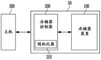
图1是图示根据本公开的实施例的包括存储器装置100的存储装置50的图。FIG. 1 is a diagram illustrating a memory device 50 including a
参考图1,存储装置50可以包括存储器装置100和存储器控制器200。Referring to FIG. 1 , the storage device 50 may include a
存储装置50可以是被配置为在主机300(例如,作为非限制性示例,蜂窝电话、智能电话、MP3播放器、膝上型计算机、台式计算机、游戏机、电视、平板电脑或车载信息娱乐系统)的控制下存储数据的装置。Storage device 50 may be configured to be stored on host computer 300 (eg, by way of non-limiting example, a cellular phone, smartphone, MP3 player, laptop computer, desktop computer, game console, television, tablet computer, or in-vehicle infotainment system) A device that stores data under the control of ).
存储装置50可以根据作为与主机300的通信系统的主机接口而被实现为各种存储装置中的任一个。例如,存储装置50可以由各种存储装置中的任一种进行配置,例如,固态驱动器(SSD)、多媒体卡(MMC)、嵌入式MMC(eMMC)、小尺寸MMC(RS-MMC)或微型MMC、安全数字卡(SD)、小型SD、微型SD类型安全数字卡、通用串行总线(USB)存储装置、通用闪存(UFS)装置、个人计算机存储器卡国际协会(PCMCIA)卡类型存储装置、外围部件互连(PCI)卡类型的存储装置、PCI快速(PCI-E)类型存储装置、紧凑型闪存(CF)卡、智能媒体卡和记忆棒。The storage device 50 may be implemented as any one of various storage devices according to a host interface as a communication system with the
存储装置50可以以各种封装类型中的任一种形式制造。例如,存储装置50可以被制造为堆叠封装(POP)类型、系统级封装(SIP)类型、片上系统(SOC)类型、多芯片封装(MCP)类型、板载芯片(COB)类型、晶圆级制造封装(WFP)类型和晶圆级堆叠封装(WSP)类型。Memory device 50 may be fabricated in any of a variety of package types. For example, the memory device 50 may be manufactured as a package-on-package (POP) type, a system-in-package (SIP) type, a system-on-chip (SOC) type, a multi-chip package (MCP) type, a chip-on-board (COB) type, a wafer level Manufactured Package (WFP) type and Wafer Level Stacked Package (WSP) type.
存储器装置100可以在其中存储数据。存储器装置100可以响应于存储器控制器200的控制或在存储器控制器200的控制下操作。存储器装置100可以包括存储器单元阵列110,存储器单元阵列110包括被配置为存储数据的多个存储器单元。存储器单元阵列110可以包括多个存储器块。每个存储器块可以包括多个存储器单元。每个存储器块可以是用于执行从存储器装置100擦除数据的操作的单位。在实施例中,存储器块可以包括多个页。每个页可以是用于执行将数据存储在存储器装置100中的编程操作或从存储器装置100读取所存储的数据的操作的单位。The
在实施例中,存储器装置100可以是双倍数据速率同步动态随机存取存储器(DDRSDRAM)、低功率双倍数据速率4(LPDDR4)SDRAM、图形双倍数据速率(GDDR)SDRAM、低功率DDR(LPDDR)、Rambus动态随机存取存储器(RDRAM)、NAND闪存、垂直NAND闪存、NOR闪存装置、电阻式随机存取存储器(RRAM)、相变存储器(PRAM)、磁阻随机存取存储器(MRAM)、铁电随机存取存储器(FRAM)或自旋转移矩随机存取存储器(STT-RAM)。在本说明书中,为了方便起见,假设存储器装置100是NAND闪存。In an embodiment, the
在实施例中,存储器装置100可以体现为三维阵列结构。本公开不仅可以应用于其中电荷存储层由导电浮栅(FG)形成的闪存,而且可以应用于其中电荷存储层由绝缘层形成的电荷陷阱闪存(CTF)存储器。In an embodiment, the
在实施例中,存储器装置100中包括的每个存储器单元可以是能够存储单个数据位的单级单元(SLC)、能够存储两个数据位的多级单元(MLC)、能够存储三个数据位的三级单元(TLC)、以及能够存储四个数据位的四级单元(QLC)中的任一个的形式。In an embodiment, each memory cell included in
存储器控制器200可以控制存储装置50的整体操作。当向存储装置50供电时,存储器控制器200可以执行固件(FW)。例如,在存储器装置100是闪存装置的情况下,存储器控制器200可以执行诸如闪存转换层(FTL)的固件,以用于控制主机300与存储器装置100之间的通信。The
如果从主机300输入写入请求,则存储器控制器200可以从主机300接收待存储的数据和用于标识对应数据的逻辑地址(LA)。存储器控制器200可以将输入的逻辑地址转换为物理地址(PA),物理地址(PA)指示存储器装置100中包括的存储器单元之中待存储数据的存储器单元的物理地址。存储器控制器200可以向存储器装置100提供用于存储数据、转换的物理地址以及待存储的数据的编程命令。If a write request is input from the
在实施例中,如果从主机300输入读取请求,则存储器控制器200可以从主机300接收用于标识待读取的数据的逻辑地址。存储器控制器200可以获得与输入的逻辑地址相对应的物理地址,并且向存储器装置100提供读取命令和物理地址。在实施例中,在擦除操作期间,存储器控制器200可以向存储器装置100提供擦除命令和物理块地址。In an embodiment, if a read request is input from the
在实施例中,在不存在来自主机300的请求的情况下,存储器控制器200可以自主地控制存储器装置100来执行编程操作、读取操作或擦除操作。例如,存储器控制器200可以控制存储器装置100以执行后台操作,诸如损耗均衡操作、垃圾收集操作和读取回收操作。In an embodiment, in the absence of a request from the
存储器控制器200可以包括随机化器210。The
随机化器210可以针对待存储在存储器装置100中的数据执行随机化操作。随机化器210可以针对从存储器装置100中读取的数据执行去随机化操作。随机化器210可以将针对待存储在存储器装置100中的数据的相同位值(0或1)的迭代最小化,并且因此减轻了存储器单元的阈值电压分布的变化。随机化器210具有本领域技术人员众所周知的结构,因此将省略其结构的进一步详细说明。The
随机化器210可以在编程操作期间执行随机化操作。例如,随机化器210可以基于指示用于存储数据的存储器单元的位置的物理地址来生成随机种子。随机化器210可以使用随机种子来生成随机序列(RS)。随机化器210可以使用所生成的随机序列(RS)针对由主机300提供的原始数据执行随机化操作。经随机化的原始数据可以是写入数据。存储器控制器200可以向存储器装置100提供写入数据。存储器装置100可以执行将写入数据存储在存储器单元中的编程操作。The
随机化器210可以在读取操作期间执行去随机化操作。随机化器210可以从存储器装置100接收作为已读取的数据的读取数据。随机化器210可以使用在随机化操作期间使用的随机序列(RS)针对读取数据执行去随机化操作。经去随机化的数据可以是从主机300提供的原始数据。
相同数据的副本可以存储在存储器装置100中包括的不同存储器单元中。例如,相同数据的副本可以存储在存储器装置100中包括的不同存储器块中。详细地,存储器装置100可以将数据存储在第一存储器块和另一个第二存储器块中以进行备份,以便应对突然的断电事件。然而,随机化器210根据待存储数据的物理地址来生成随机种子。因此,尽管待存储在不同存储器块中的数据是相同的数据,但是可以使用不同的随机种子来将待存储在不同存储器块中的数据随机化。因此,为了在读取之后将存储用于备份的数据存储在存储器装置100中包括的特定存储器块中,存储器装置100必须读取存储用于备份的数据,并且随机化器210必须针对读取数据执行去随机化操作并且恢复其原始数据。然后,随机化器210可以使用不同的随机种子将所恢复的原始数据随机化,并且将经随机化的数据存储在存储器装置100中。这样,如果使用不同的随机种子针对相同的原始数据执行随机化操作以及然后将原始数据的副本存储在不同存储器块中,则使用对应数据的应用可能受到限制。Copies of the same data may be stored in different memory units included in
根据本公开的实施例,如果相同的原始数据存储在不同的存储器块中,则随机化器210可以使用相同的随机种子执行随机化操作。因此,不需要执行将用于备份的数据去随机化以恢复原始数据的操作。因此,可以促进存储器装置100中的使用数据的数据应用。According to an embodiment of the present disclosure, if the same original data is stored in different memory blocks, the
主机300可以使用各种通信方法(例如,通用串行总线(USB)、串行AT附件(SATA)、串行附件SCSI(SAS)、高速芯片间(HSIC)、小型计算机系统接口(SCSI)、外围部件互连(PCI)、PCI快速(PCIe)、非易失性存储器快速(NVMe)、通用闪存(UFS)、安全数字(SD)、多媒体卡(MMC)、嵌入式MMC(eMMC)、双列直插式存储器模块(DIMM)、注册DIMM(RDIMM)和负载减少的DIMM(LRDIMM)通信方法)中的至少一个与存储装置50通信。The
图2是图示根据本公开的实施例的存储器装置100的结构的图。FIG. 2 is a diagram illustrating the structure of the
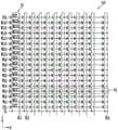
参考图2,存储器装置100可以包括存储器单元阵列110、外围电路120和控制逻辑130。Referring to FIG. 2 , the
存储器单元阵列110可以包括多个存储器块BLK1至BLKz。多个存储器块BLK1至BLKz通过行线RL耦合到行解码器121。多个存储器块BLK1至BLKz可以通过位线BL1至BLm耦合到页缓冲器组123。存储器块BLK1至BLKz中的每一个可以包括多个存储器单元。在实施例中,多个存储器单元可以是非易失性存储器单元。耦合到同一字线的存储器单元可以被定义为一个页。因此,每个存储器块可以包括多个页。The
行线RL可以包括至少一个源极选择线、多个字线和至少一个漏极选择线。The row lines RL may include at least one source select line, a plurality of word lines, and at least one drain select line.
存储器单元阵列110中包括的每个存储器单元可以由能够存储单个数据位的单级单元(SLC)、能够存储两个数据位的多级单元(MLC)、能够存储三个数据位的三级单元(TLC)或者能够存储四个数据位的四级单元(QLC)形成。Each memory cell included in the
外围电路120可以在控制逻辑130的控制下对存储器单元阵列110的选定区域执行编程操作、读取操作或擦除操作。外围电路120可以驱动存储器单元阵列110。例如,外围电路120可以在控制逻辑130的控制下向行线RL和位线BL1至BLn施加各种操作电压,或者释放所施加的电压。The
外围电路120可以包括行解码器121、电压发生器122、页缓冲器组123、列解码器124和输入/输出电路125。The
行解码器121通过行线RL耦合到存储器单元阵列110。行线RL可以包括至少一个源极选择线、多个字线和至少一个漏极选择线。在实施例中,字线可以包括普通字线和虚设字线。在实施例中,行线RL可以进一步包括管道选择线。
行解码器121可以在控制逻辑130的控制下操作。行解码器121可以从控制逻辑130接收行地址RADD。
行解码器121可以对行地址RADD进行解码。行解码器121可以响应于经解码的地址来选择存储器块BLK1至BLKz中的至少一个存储器块。行解码器121可以响应于经解码的地址来选择所选择的存储器块的至少一个字线WL,使得从电压发生器122生成的电压被施加到至少一个字线WL。The
例如,在编程操作期间,行解码器121可以将编程电压施加到所选择的字线并且将具有比编程电压的水平更低的水平的编程通过电压施加到未选择的字线。在编程验证操作期间,行解码器121可以将验证电压施加到所选择的字线并且将比验证电压更高的验证通过电压施加到未选择的字线。在读取操作期间,行解码器121可以将读取电压施加到所选择的字线,并且将比读取电压更高的读取通过电压施加到未选择的字线。For example, during a programming operation,
在实施例中,可以基于存储器块来执行存储器装置100的擦除操作。在擦除操作期间,行解码器121可以响应于经解码的地址来选择一个存储器块。在擦除操作期间,行解码器121可以将接地电压施加到耦合到所选择的存储器块的字线。In an embodiment, the erase operation of the
电压发生器122可以在控制逻辑130的控制下操作。电压发生器122可以使用提供给存储器装置100的外部电源电压来生成多个电压。详细地,电压发生器122可以响应于操作信号OPSIG,生成用于编程操作、读取操作和擦除操作的各种操作电压Vop。例如,电压发生器122可以在控制逻辑130的控制下生成编程电压、验证电压、通过电压、读取电压、擦除电压等。
在实施例中,电压发生器122可以通过调节外部电源电压来生成内部电源电压。从电压发生器122生成的内部电源电压可以用作存储器装置100的操作电压。In an embodiment, the
在实施例中,电压发生器122可以使用外部电源电压或内部电源电压来生成多个电压。In an embodiment, the
例如,电压发生器122可以包括用于接收内部电源电压的多个泵浦电容器,并且通过在控制逻辑130的控制下选择性地激活多个泵浦电容器来生成多个电压。For example, the
所生成的电压可以由行解码器121提供给存储器单元阵列110。The generated voltages may be provided to the
页缓冲器组123可以包括第一页缓冲器PB1至第n页缓冲器PBn。第一页缓冲器PB1至第n页缓冲器PBn分别通过第一位线BL1至第n位线BLn耦合到存储器单元阵列110。第一页缓冲器PB1至第n页缓冲器PBn可以在控制逻辑130的控制下操作。第一页缓冲器PB1至第n页缓冲器PBn可以响应于页缓冲器控制信号PBSIGNALS而操作。例如,第一页缓冲器PB1至第n页缓冲器PBn可以临时存储通过第一位线BL1至第n位线BLn接收的数据,或者在读取操作或验证操作期间感测第一位线BL1至第n位线BLn的电压或电流。The
在编程操作期间,当编程脉冲被施加到所选择的字线时,第一页缓冲器PB1至第n页缓冲器PBn可以将通过数据输入/输出电路125接收的数据DATA通过第一位线BL1至第n位线BLn传输至所选择的存储器单元。基于所传输的数据,对所选择的页中的存储器单元进行编程。耦合到施加有编程使能电压(例如,接地电压)的位线的存储器单元可以具有增加的阈值电压。可以保持耦合到施加有编程禁止电压(例如,电源电压)的位线的存储器单元的阈值电压。在编程验证操作期间,第一页缓冲器PB1至第n页缓冲器PBn可以通过第一位线BL1至第n位线BLn从所选择的存储器单元读取页数据。During a program operation, when a program pulse is applied to a selected word line, the first to n-th page buffers PB1 to PBn may pass data DATA received through the data input/
在读取操作期间,第一页缓冲器PB1至第n页缓冲器PBn可以通过第一位线BL1至第n位线BLn从所选择的页的存储器单元读取数据DATA,并且在列解码器124的控制下将所读取的数据DATA输出至数据输入/输出电路125。During a read operation, the first to n-th page buffers PB1 to PBn may read data DATA from the memory cells of the selected page through the first to n-th bit lines BL1 to BLn, and the column decoder The read data DATA is output to the data input/
在擦除操作期间,第一页缓冲器PB1至第n页缓冲器PBn可以将第一位线BL1至第n位线BLn浮置。During an erase operation, the first to n-th page buffers PB1 to PBn may float the first to n-th bit lines BL1 to BLn.
列解码器124可以响应于列地址CADD而在输入/输出电路125和页缓冲器组123之间传输数据。例如,列解码器124可以通过数据线DL与第一页缓冲器PB1至第n页缓冲器PBn交换数据,或者可以通过列线CL与输入/输出电路125交换数据。The
输入/输出电路125可以将从参考图1描述的存储器控制器200接收的命令CMD或地址ADDR传输到控制逻辑130,或者可以与列解码器124交换数据DATA。The input/
在读取操作或验证操作期间,感测电路126可以响应于使能位信号VRYBIT来生成参考电流、将从页缓冲器组123接收的感测电压VPB与由参考电流生成的参考电压进行比较,并且输出通过信号PASS或失败信号FAIL。During a read operation or a verify operation, the
控制逻辑130可以响应于命令CMD和地址ADD而输出操作信号OPSIG、行地址RADD、页缓冲器控制信号PBSIGNALS和使能位信号VRYBIT,并且因此控制外围电路120。另外,控制逻辑130可以响应于通过信号PASS或失败信号FAIL来确定目标存储器单元在验证操作期间是否已通过验证。The
图3是图示根据本公开的实施例的图2的多个存储器块BLK1至BLKz中的任一个存储器块BLKn的结构的图。FIG. 3 is a diagram illustrating a structure of any one memory block BLKn of the plurality of memory blocks BLK1 to BLKz of FIG. 2 according to an embodiment of the present disclosure.
参考图3,在存储器块BLKn中,彼此平行布置的多个字线可以耦合在第一选择线和第二选择线之间。在此,第一选择线可以是源极选择线SSL,并且第二选择线可以是漏极选择线DSL。更详细地,存储器块BLKn可以包括耦合在位线BL1至BLn与源极线SL之间的多个串ST。图3的位线BL1至BLn可以是图2的第一位线BL1至第n位线BLn。位线BL1至BLn可以分别耦合到串ST,并且源极线SL可以公共地耦合到串ST。串ST可以具有相同的配置;因此,作为示例,将详细描述耦合到第一位线BL1的串ST。Referring to FIG. 3 , in the memory block BLKn, a plurality of word lines arranged in parallel with each other may be coupled between the first selection line and the second selection line. Here, the first selection line may be a source selection line SSL, and the second selection line may be a drain selection line DSL. In more detail, the memory block BLKn may include a plurality of strings ST coupled between the bit lines BL1 to BLn and the source line SL. The bit lines BL1 to BLn of FIG. 3 may be the first bit line BL1 to the nth bit line BLn of FIG. 2 . The bit lines BL1 to BLn may be coupled to the strings ST, respectively, and the source lines SL may be commonly coupled to the strings ST. The strings ST may have the same configuration; therefore, as an example, the string ST coupled to the first bit line BL1 will be described in detail.
串ST可以包括在源极线SL和第一位线BLl之间彼此串联耦合的源极选择晶体管SST、多个存储器单元MC1至MC16和漏极选择晶体管DST。至少一个源极选择晶体管SST和至少一个漏极选择晶体管DST可以被包括在每个串ST中。图3所示的存储器单元MC1至MC16的数目不受限制,并且本公开考虑了在每个串ST中包括更多数目的存储器单元的其他实施例。The string ST may include a source selection transistor SST, a plurality of memory cells MC1 to MC16, and a drain selection transistor DST coupled in series with each other between the source line SL and the first bit line BL1. At least one source selection transistor SST and at least one drain selection transistor DST may be included in each string ST. The number of memory cells MC1 to MC16 shown in FIG. 3 is not limited, and the present disclosure contemplates other embodiments including a greater number of memory cells in each string ST.
源极选择晶体管SST的源极可以耦合至源极线SL,而漏极选择晶体管DST的漏极可以耦合至第一位线BLl。存储器单元MC1至MC16可以串联耦合在源极选择晶体管SST和漏极选择晶体管DST之间。不同串ST中包括的源极选择晶体管SST的栅极可以耦合至源极选择线SSL,漏极选择晶体管DST的栅极可以耦合至漏极选择线DSL,并且存储器单元MC1至MC16的栅极可以分别耦合到多个字线WL1至WL16。在不同串ST中包括的存储器单元之中,与每个字线耦合的存储器单元组可以被称为物理页PG。因此,在存储器块BLKn中包括的物理页PG的数目可以对应于字线WL1至WL16的数目。图3中所示的源极线SL、源极选择线SSL、字线WL1至WL16以及漏极选择线DSL可以被包括在图2的行线RL中。漏极选择线DSL、第一字线WL1至第十六字线WL16以及源极选择线SSL由行解码器121控制。源极线SL由控制逻辑130控制。The source of the source select transistor SST may be coupled to the source line SL, and the drain of the drain select transistor DST may be coupled to the first bit line BL1. The memory cells MC1 to MC16 may be coupled in series between the source select transistor SST and the drain select transistor DST. The gates of the source select transistors SST included in the different strings ST may be coupled to the source select line SSL, the gates of the drain select transistors DST may be coupled to the drain select line DSL, and the gates of the memory cells MC1 to MC16 may be coupled to the drain select line DSL. are coupled to a plurality of word lines WL1 to WL16, respectively. Among memory cells included in different strings ST, a group of memory cells coupled to each word line may be referred to as a physical page PG. Therefore, the number of physical pages PG included in the memory block BLKn may correspond to the number of word lines WL1 to WL16. The source line SL, the source selection line SSL, the word lines WL1 to WL16 and the drain selection line DSL shown in FIG. 3 may be included in the row line RL of FIG. 2 . The drain selection line DSL, the first to sixteenth word lines WL1 to WL16 and the source selection line SSL are controlled by the
如果存储器单元是能够存储一位数据的单级单元(SLC),则对应的物理页PG可以存储一个逻辑页(LPG)的数据。每个存储器单元可以存储两个或更多个数据位,并且在这种情况下,每个物理页PG可以存储两个或更多个LPG的数据。If the memory cell is a single-level cell (SLC) capable of storing one bit of data, the corresponding physical page PG can store data of one logical page (LPG). Each memory cell can store two or more data bits, and in this case, each physical page PG can store data of two or more LPGs.
图4是图示根据本公开的实施例的可以在将数据存储在存储器装置中的方法中使用的模糊-精细(foggy-fine)编程操作的图。图4的水平轴表示存储器单元的阈值电压,并且图4的垂直轴表示存储器单元的数目。4 is a diagram illustrating a foggy-fine programming operation that may be used in a method of storing data in a memory device according to an embodiment of the present disclosure. The horizontal axis of FIG. 4 represents the threshold voltage of the memory cells, and the vertical axis of FIG. 4 represents the number of memory cells.
将描述能够在一个存储器单元中存储三位数据的三级单元TLC作为代表性示例。存储器单元中的每一个可以具有擦除状态E或者第一编程状态P1至第七编程状态P7中的任一个作为目标编程状态。可以根据待存储在存储器单元中的数据来确定目标编程状态。A three-level cell TLC capable of storing three bits of data in one memory cell will be described as a representative example. Each of the memory cells may have an erased state E or any one of the first to seventh programming states P1 to P7 as a target programming state. The target programming state may be determined from the data to be stored in the memory cell.
图4图示了相对于存储器单元中存储的数据位数的阈值电压分布Vth。图4包括当执行模糊编程操作时的阈值电压分布和当执行精细编程操作时的阈值电压分布。模糊编程操作可以包括模糊编程电压施加操作和模糊验证操作。精细编程操作可以包括精细编程电压施加操作和精细验证操作。在模糊编程操作期间使用的模糊验证电压Vfg可以低于在精细编程操作期间使用的精细验证电压Vfn。精细验证电压Vfn可以与对应于相关联的目标编程状态的验证电压相同。FIG. 4 illustrates the threshold voltage distribution Vth with respect to the number of bits of data stored in the memory cell. FIG. 4 includes a threshold voltage distribution when a fuzzy programming operation is performed and a threshold voltage distribution when a fine programming operation is performed. The fuzzy programming operation may include a fuzzy programming voltage applying operation and a fuzzy verifying operation. The fine programming operation may include a fine programming voltage applying operation and a fine verifying operation. The fuzzy verification voltage Vfg used during the fuzzy programming operation may be lower than the fine verification voltage Vfn used during the fine programming operation. The fine verify voltage Vfn may be the same as the verify voltage corresponding to the associated target programming state.
图5是图示根据本公开的实施例的在存储器块中执行模糊-精细编程操作的序列的图。5 is a diagram illustrating a sequence of performing fuzzy-fine programming operations in a memory block according to an embodiment of the present disclosure.
参考图5,可以对多个字线中的每一个执行模糊编程操作和精细编程操作。可以在字线号增加的方向上执行编程操作。在实施例中,模糊编程操作和精细编程操作可以单独地执行。例如,如果完成了对WL1的模糊编程操作,则可以对相邻的字线WL2执行模糊编程操作。如果完成了对WL2的模糊编程操作,则可以对WL1执行精细编程操作。如果完成了对WL1的精细编程操作,则可以对WL3执行模糊编程操作。如果完成了对WL3的模糊编程操作,则可以对WL2执行精细编程操作。换言之,对第N字线WL N执行精细编程操作,此后,如果完成了对WL N的精细编程操作,则可以对WL N+2执行模糊编程操作。如果完成了对WL N+2的模糊编程操作,则可以对WL N+1执行精细编程操作。如果完成了对WL N+1的精细编程操作,则可以对WL N+3执行模糊编程操作。如果完成了对WL N+3的模糊编程操作,则可以对WL N+2执行精细编程操作。以此方式,可以对存储器单元阵列110中的多个字线交替地执行模糊-精细编程操作。Referring to FIG. 5, a fuzzy programming operation and a fine programming operation may be performed on each of a plurality of word lines. Program operations can be performed in the direction of increasing word line numbers. In an embodiment, fuzzy programming operations and fine programming operations may be performed separately. For example, if the fuzzy programming operation on WL1 is completed, the fuzzy programming operation may be performed on the adjacent word line WL2. If the fuzzy programming operation for WL2 is completed, the fine programming operation for WL1 can be performed. If the fine programming operation on WL1 is completed, the fuzzy programming operation can be performed on WL3. If the fuzzy programming operation for WL3 is completed, the fine programming operation for WL2 can be performed. In other words, the fine programming operation is performed on the Nth word line WL N, and thereafter, if the fine programming operation on WL N is completed, the fuzzy programming operation may be performed on WL N+2. If the fuzzy programming operation for WL N+2 is completed, the fine programming operation for WL N+1 can be performed. If the fine programming operation on WL N+1 is completed, the fuzzy programming operation can be performed on WL N+3. If the fuzzy programming operation for WL N+3 is completed, the fine programming operation for WL N+2 can be performed. In this manner, fuzzy-fine programming operations may be alternately performed on a plurality of word lines in the
如果在执行针对待存储在WL N+2中的数据的模糊编程之后并且在执行精细编程之前发生突然断电事件,则可能丢失待存储在WL N+2中的数据。因此,需要存储器装置存储待存储在WL N+2中的数据以用于备份,以应对突然断电事件。The data to be stored in WL N+2 may be lost if a sudden power-off event occurs after performing fuzzy programming for data to be stored in WL N+2 and before performing fine programming. Therefore, a memory device is required to store the data to be stored in WL N+2 for backup in case of a sudden power outage event.
在这种情况下,因为相同的数据存储在不同的存储器块中,不同的随机种子可能被使用。根据本公开的实施例,如果相同的数据存储在不同的存储器块中,则随机化器210可以使用相同的随机种子来执行随机化操作。因此,可以增强模糊-精细编程操作的效率。In this case, because the same data is stored in different memory blocks, different random seeds may be used. According to an embodiment of the present disclosure, if the same data is stored in different memory blocks, the
图6是图示根据本公开的实施例的将相同数据写入多个存储器块BLK1至BLK2或从中读取相同数据的过程的图。FIG. 6 is a diagram illustrating a process of writing the same data to or reading the same data from a plurality of memory blocks BLK1 to BLK2 according to an embodiment of the present disclosure.
响应于主机300的写入请求,可以将原始数据DATA输入到存储器控制器200中包括的随机化器210。所输入的原始数据DATA可以通过随机化操作转换为写入数据WDATA。随机化操作可以包括通过将原始数据与随机种子SEED组合来生成经转换的数据的各种方法。写入数据WDATA可以存储在第一存储器块BLK1和第二存储器块BLK2的至少一个存储器块中。第一存储器块BLK1中存储的写入数据WDATA可以是与第二存储器块BLK2中存储的写入数据WDATA相同的数据。The original data DATA may be input to the
读取数据RDATA可以从存储器单元阵列110输出。存储器单元阵列110可以包括多个存储器块BLK1至BLKz。例如,多个存储器块BLK1至BLKz可以包括第一存储器块BLK1和第二存储器块BLK2。读取数据RDATA可以从第一存储器块BLK1和第二存储器块BLK2中的任一个读取和输出。所输出的读取数据RDATA可以输入到随机化器210。所输入的读取数据RDATA可以通过去随机化操作转换为原始数据DATA。去随机化操作可以包括通过将经转换的数据与随机种子SEED组合来生成原始数据的各种方法。The read data RDATA may be output from the
图7是图示根据本公开的实施例的在写入操作期间操作随机化器210的方法的图。FIG. 7 is a diagram illustrating a method of operating the
参考图7,随机化器210可以包括随机种子生成器211、操作部件212和随机表213。从存储器控制器200获得的物理地址可以是指示第一存储器块BLK1中包括的存储器单元的地址的第一物理地址和指示第二存储器块BLK2中包括的存储器单元的地址的第二物理地址中的至少一个。经转换的物理地址可以输入到随机种子生成器211。随机种子生成器211可以参考随机表213来获得随机种子SEED,并且将随机种子SEED输出到操作部件212。操作部件212可以使用所接收的原始数据DATA和所接收的随机种子SEED来执行随机化操作。作为执行随机化操作的结果,可以生成写入数据WDATA。可以从随机化器210输出写入数据WDATA。写入数据WDATA可以存储在存储器单元阵列110中包括的多个存储器块BLK1至BLKz中的至少一个中。Referring to FIG. 7 , the
在本公开的实施例中,当第一物理地址和第二物理地址均被输入时,随机种子生成器211可以选择任一物理地址。例如,所选择的物理地址可以是第二物理地址。随机种子生成器211可以参考随机表213来获得与所选择的物理地址相对应的随机种子SEED,并且将随机种子SEED输出到操作部件212。操作部件212可以使用所接收的原始数据DATA和所接收的随机种子SEED执行随机化操作。作为执行随机化操作的结果,可以生成写入数据WDATA。可以从随机化器210输出写入数据WDATA。写入数据WDATA可以存储在存储器单元阵列110中包括的与第二物理地址相对应的多个存储器块BLK1至BLKz中。In an embodiment of the present disclosure, when both the first physical address and the second physical address are input, the
图8是图示根据本公开的实施例的在读取操作期间操作随机化器210的方法的图。FIG. 8 is a diagram illustrating a method of operating the
参考图8,随机化器210可以包括随机种子生成器211、操作部件212和随机表213。存储器控制器200可以响应于来自主机的读取请求来接收读取数据RDATA和物理地址。所接收的物理地址可以输入到随机种子生成器211。随机种子生成器211可以参考随机表213来获得随机种子SEED,并且将随机种子SEED输出到操作部件212。操作部件212可以使用所接收的读取数据RDATA和所接收的随机种子SEED来执行去随机化操作。作为执行去随机化操作的结果,可以生成原始数据DATA。原始数据DATA可以从随机化器210输出。输出数据可以提供给主机。Referring to FIG. 8 , the
图9是图示根据本公开的实施例的多个存储器块BLK1至BLKz的物理地址之间的关系的图。FIG. 9 is a diagram illustrating a relationship between physical addresses of a plurality of memory blocks BLK1 to BLKz according to an embodiment of the present disclosure.
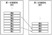
响应于来自主机的写入请求,相同的数据可以存储在多个存储器块BLK1至BLKz中。例如,假定相同的数据存储在由SLC存储器单元形成的第一存储器块SLC和由QLC存储器单元形成的第二存储器块QLC中。第一存储器块可以包括多个页,并且每个页可以包括多个存储器单元。数据可以存储在每个存储器单元中。第二存储器块可以包括多个页,并且每个页可以包括多个存储器单元。数据可以存储在每个存储器单元中。The same data may be stored in a plurality of memory blocks BLK1 to BLKz in response to a write request from the host. For example, it is assumed that the same data is stored in a first memory block SLC formed by SLC memory cells and a second memory block QLC formed by QLC memory cells. The first memory block may include multiple pages, and each page may include multiple memory cells. Data can be stored in each memory cell. The second memory block may include multiple pages, and each page may include multiple memory cells. Data can be stored in each memory cell.
参考图9,指示数据存储在第一存储器块中的位置的物理地址可以由SWL1、SWL2、SWL3、SWL4等表示。指示数据存储在第二存储器块中的位置的物理地址可以由QWL1、QWL2、QWL3、QWL4等表示。第一存储器块中包括的每个存储器单元可以存储一个数据位,并且第二存储器块中包括的每个存储器单元可以存储四个数据位。因此,当假设相同的数据存储在由SLC存储器单元形成的第一存储器块和由QLC存储器单元形成的第二存储器块中时,四个SLC存储器块中存储的数据可以与一个QLC存储器块中存储的数据相同。换言之,第一存储器块的四个物理地址可以对应于第二存储器块的一个物理地址。例如,具有物理地址SWL1、SWL2、SWL3和SWL4的存储器单元中包括的数据可以与具有物理地址QWL1的存储器单元中包括的数据相同。作为另一示例,具有物理地址SWL5、SWL6、SWL7和SWL8的存储器单元中包括的数据可以与具有物理地址QWL2的存储器单元中包括的数据相同。Referring to FIG. 9, physical addresses indicating where data is stored in the first memory block may be represented by SWL1, SWL2, SWL3, SWL4, and the like. Physical addresses indicating where data is stored in the second memory block may be represented by QWL1, QWL2, QWL3, QWL4, and so on. Each memory cell included in the first memory block may store one bit of data, and each memory cell included in the second memory block may store four bits of data. Therefore, when it is assumed that the same data is stored in the first memory block formed by the SLC memory cells and the second memory block formed by the QLC memory cells, the data stored in the four SLC memory blocks can be stored in the same QLC memory block as data are the same. In other words, the four physical addresses of the first memory block may correspond to one physical address of the second memory block. For example, the data included in the memory cells having the physical addresses SWL1, SWL2, SWL3, and SWL4 may be the same as the data included in the memory cell having the physical address QWL1. As another example, data included in memory cells having physical addresses SWL5, SWL6, SWL7, and SWL8 may be the same as data included in memory cells having physical address QWL2.
图10是图示根据本公开的实施例的随机表213的图。FIG. 10 is a diagram illustrating the random table 213 according to an embodiment of the present disclosure.
随机表213可以包括指示第一存储器块中包括的存储器单元的物理地址的SLC地址和指示第二存储器块中包括的存储器单元的物理地址的QLC地址。此外,随机表213可以包括与相应QLC地址相对应的随机种子SEED。尽管为了说明的目的,图示了其中随机表包括八个SLC地址的示例,但是本领域技术人员将理解,可以增加随机表213中包括的物理地址的数目。The random table 213 may include SLC addresses indicating physical addresses of memory cells included in the first memory block and QLC addresses indicating physical addresses of memory cells included in the second memory block. Additionally, the random table 213 may include a random seed SEED corresponding to the corresponding QLC address. Although an example in which the random table includes eight SLC addresses is illustrated for illustrative purposes, those skilled in the art will appreciate that the number of physical addresses included in the random table 213 may be increased.
如图9所示,四个SLC物理地址可以对应于一个QLC物理地址。一个随机种子SEED可以对应于一个QLC物理地址。例如,SLC物理地址中的SWL1、SWL2、SWL3和SWL4可以对应于QLC物理地址中的QWL1。可以获得SQW1,SQW1是与QWL1相对应的随机种子SEED。在另一示例中,SLC物理地址中的SWL5、SWL6、SWL7和SWL8可以对应于QLC物理地址中的QWL2。可以获得SQW2,SQW2是与QWL2相对应的随机种子SEED。As shown in FIG. 9, four SLC physical addresses may correspond to one QLC physical address. A random seed SEED can correspond to a QLC physical address. For example, SWL1, SWL2, SWL3, and SWL4 in the SLC physical address may correspond to QWL1 in the QLC physical address. SQW1 can be obtained, SQW1 is the random seed SEED corresponding to QWL1. In another example, SWL5, SWL6, SWL7, and SWL8 in the SLC physical address may correspond to QWL2 in the QLC physical address. SQW2 can be obtained, SQW2 is the random seed SEED corresponding to QWL2.
如果待输入到随机种子生成器211的物理地址是SWL1,则随机种子生成器211可以通过参考随机表213来获得与QLC物理地址相对应的QWL1,并且可以获得SQW1,SQW1是与QWL1相对应的随机种子SEED。如果待输入到随机种子生成器211的物理地址是SWL2,则随机种子生成器211可以参考随机表213来获得与QLC物理地址相对应的QWL1,并且可以获得SQW1,与QWL1相对应的随机种子SEED。如果待输入到随机种子生成器211的物理地址是SWL3,则随机种子生成器211可以参考随机表213来获得QWL1,并且可以获得SQW1,QWL1是对应的QLC物理地址,SQW1是与QWL1相对应的随机种子SEED。如果待输入到随机种子生成器211的物理地址是SWL4,则随机种子生成器211可以通过参考随机表213来获得与QLC物理地址相对应的QWL1,并且可以获得SQW1,SQW1是与QWL1相对应的随机种子SEED。If the physical address to be input to the
如果待输入到随机种子生成器211的物理地址是SWL5,则随机种子生成器211可以参考随机表213来获得QWL2,并且可以获得SQW2,QWL2是对应的QLC物理地址,SQW2是与QWL2相对应的随机种子SEED。如果待输入到随机种子生成器211的物理地址是SWL6,则随机种子生成器211可以参考随机表213来获得与QLC物理地址相对应的QWL2,并且可以获得SQW2,SQW2是与QWL2相对应的随机种子SEED。如果待输入到随机种子生成器211的物理地址是SWL7,则随机种子生成器211可以参考随机表213来获得与QLC物理地址相对应的QWL2,并且可以获得SQW2,与QWL2相对应的随机种子SEED。如果待输入到随机种子生成器211的物理地址是SWL8,则随机种子生成器211可以参考随机表213来获得QWL2,并且可以获得SQW2,QWL2是对应的QLC物理地址,SQW2是与QWL2相对应的随机种子SEED。If the physical address to be input to the
所获得的随机种子SEED可以输入到操作部件,并且在随机化操作中被使用。The obtained random seed SEED can be input to the operation part and used in the randomization operation.
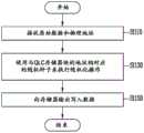
图11是详细图示根据本公开的实施例的当从主机接收写入请求时,使用随机化器210来执行生成和输出写入数据的操作的方法的流程图。11 is a flowchart illustrating in detail a method of performing an operation of generating and outputting write data using the
在步骤S1110处,存储器控制器200可以接收原始数据DATA和物理地址。物理地址可以是第一物理地址和第二物理地址中的至少一个。第一物理地址可以是指示第一存储器块中包括的存储器单元的地址。第二物理地址可以是指示第二存储器块中包括的存储器单元的地址。At step S1110, the
在步骤S1130处,原始数据DATA和物理地址可以输入到随机化器210。如果所输入的物理地址是指示SLC块中包括的存储器单元的地址,则随机化器210可以检查对应QLC存储器块的地址,并且使用与QLC存储器块的地址相对应的随机种子SEED来执行随机化操作。如果所输入的物理地址是指示QLC块中包括的存储器单元的地址,则随机化器210可以使用与QLC存储器块的地址相对应的随机种子SEED来执行随机化操作。At step S1130 , the original data DATA and the physical address may be input to the
在步骤S1150处,作为执行随机化操作的结果而生成的写入数据WDATA可以输出到存储器装置100。存储器装置100可以接收写入数据WDATA,并且将写入数据WDATA存储在与所输入的物理地址相对应的存储器单元中。At step S1150 , the write data WDATA generated as a result of performing the randomization operation may be output to the
图12是图示根据本公开的实施例的获得图11的随机种子并且执行随机化操作的方法的流程图。12 is a flowchart illustrating a method of obtaining the random seed of FIG. 11 and performing a randomization operation, according to an embodiment of the present disclosure.
参考图12,在步骤S1210处,原始数据DATA和物理地址可以输入到存储器控制器200中包括的随机化器210。物理地址可以输入到随机化器210中包括的随机种子生成器211。当所输入的物理地址是指示SLC存储器块中包括的存储器单元的地址时,随机种子生成器211可以参考随机表213来检查与SLC存储器块的地址相对应的QLC存储器块的地址。Referring to FIG. 12 , at step S1210 , the original data DATA and the physical address may be input to the
在步骤S1230处,可以获得与在步骤S1210处检查的QLC存储器块的地址相对应的随机种子SEED。At step S1230, a random seed SEED corresponding to the address of the QLC memory block checked at step S1210 can be obtained.
在步骤S1250处,所获得的随机种子SEED和原始数据DATA输入到操作部件212。操作部件212可以使用所获得的随机种子SEED和原始数据DATA来执行随机化操作。At step S1250, the obtained random seed SEED and original data DATA are input to the
图13是图示根据本公开的实施例的图1的存储器控制器的实施例的图。FIG. 13 is a diagram illustrating an embodiment of the memory controller of FIG. 1 according to an embodiment of the present disclosure.
存储器控制器1000耦合到主机和存储器装置。响应于来自主机的请求,存储器控制器1000可以访问存储器装置。The
参考图13,存储器控制器1000可以包括处理器1010、存储器缓冲器1020、纠错码(ECC)电路1030、主机接口1040、缓冲器控制电路1050、存储器接口1060和总线1070。13 , the
总线1070可以在存储器控制器1000的部件之间提供通道。The
处理器1010可以控制存储器控制器1000的整体操作并且执行逻辑操作。处理器1010可以通过主机接口1040与外部主机通信,并且可以通过存储器接口1060与存储器装置通信。此外,处理器1010可以通过缓冲器控制电路1050与存储器缓冲器1020通信。处理器1010可以通过使用存储器缓冲器1020作为操作存储器、高速缓存存储器或缓冲存储器来控制存储装置的操作。The
处理器1010可以执行闪存转换层(FTL)的功能。处理器1010可以将从主机接收的数据随机化。例如,处理器1010可以使用随机种子来将从主机接收的数据随机化。经随机化的数据可以被提供给存储器装置作为待存储的数据,并且可以被编程到存储器单元阵列。The
处理器1010可以在读取操作期间将从存储器装置接收的数据去随机化。例如,处理器1010可以使用随机种子来将从存储器装置接收的数据去随机化。经去随机化的数据可以被输出到主机。The
在实施例中,处理器1010可以驱动软件或固件来执行随机化操作或去随机化操作。In an embodiment, the
存储器缓冲器1020可以用作处理器1010的操作存储器、高速缓存存储器或缓冲存储器。存储器缓冲器1020可以存储待由处理器1010执行的代码和命令。存储器缓冲器1020可以存储待由处理器1010处理的数据。存储器缓冲器1020可以包括静态RAM(SRAM)或动态RAM(DRAM)。The
ECC电路1030可以执行纠错。ECC电路1030可以基于待通过存储器接口1060写入存储器装置的数据来执行ECC编码操作。经ECC编码的数据可以通过存储器接口1060传输到存储器装置。ECC电路1030可以对通过存储器接口1060从存储器装置接收的数据执行ECC解码操作。例如,ECC电路1030可以被包括在存储器接口1060中以作为存储器接口1060的部件。The
主机接口1040可以在处理器1010的控制下与外部主机通信。主机接口1040可以使用各种通信方法(诸如通用串行总线(USB)、串行AT附件(SATA)、串行连接的SCSI(SAS)、高速芯片间(HSIC)、小型计算机系统接口(SCSI)、外围部件互连(PCI)、PCI快速(PCIe)、非易失性存储器快速(NVMe)、通用闪存(UFS)、安全数字(SD)、多媒体卡(MMC)、嵌入式MMC(eMMC)、双列直插式存储器模块(DIMM)、注册DIMM(RDIMM)和负载减小的DIMM(LRDIMM)通信方法)中的至少一个来执行通信。The
缓冲器控制电路1050可以在处理器1010的控制下控制存储器缓冲器1020。The
存储器接口1060可以在处理器1010的控制下与存储器装置100通信。存储器接口1060可以通过通道来与存储器装置通信命令、地址和数据。The
例如,存储器控制器1000不包括存储器缓冲器1020也不包括缓冲器控制电路1050。For example, the
例如,处理器1010可以使用代码来控制存储器控制器1000的操作。处理器1010可以从存储器控制器1000中提供的非易失性存储器装置(例如,只读存储器)中加载代码。备选地,处理器1010可以通过存储器接口1060从存储器装置加载代码。For example, the
例如,存储器控制器1000的总线1070可以被划分为控制总线和数据总线。数据总线可以在存储器控制器1000中传输数据。控制总线可以在存储器控制器1000中传输诸如命令和地址的控制信息。数据总线和控制总线可以彼此分离并且可以不彼此干扰也不互相影响。数据总线可以耦合到主机接口1040、缓冲器控制电路1050、ECC电路1030和存储器接口1060。控制总线可以耦合到主机接口1040、处理器1010、缓冲器控制电路1050、存储器缓冲器1020和存储器接口1060。For example, the
图14是图示应用了包括根据本公开的实施例的存储器装置的存储装置的存储器卡系统2000的框图。14 is a block diagram illustrating a
参考图14,存储器卡系统2000可以包括存储器控制器2100、存储器装置2200和连接器2300。Referring to FIG. 14 , a
存储器控制器2100耦合到存储器装置2200。存储器控制器2100可以访问存储器装置2200。存储器控制器2100可以以与参考图1描述的存储器控制器200相同的方式实现。
在实施例中,存储器控制器2100可以包括诸如随机存取存储器(RAM)、处理单元、主机接口和存储器接口以及ECC电路的部件。In an embodiment, the
存储器控制器2100可以通过连接器2300与外部装置通信。存储器控制器2100可以基于特定的通信协议与外部装置(例如,主机)通信。在实施例中,存储器控制器2100可以通过各种通信协议(作为非限制性示例,诸如通用串行总线(USB)、多媒体卡(MMC)、嵌入式MMC(eMMC)、外围部件互连(PCI)、PCI-快速(PCI-E)、高级技术附件(ATA)、串行ATA(SATA)、并行ATA(PATA)、小型计算机小型接口(SCSI)、增强型小型磁盘接口(ESDI)、集成驱动电子装置(IDE)、火线、通用闪存(UFS)、Wi-Fi、蓝牙和非易失性存储器快速(NVMe)协议)中的至少一个与外部装置通信。在实施例中,连接器2300可以由上述各种通信协议中的至少一个来被限定。The
在实施例中,存储器装置2200可以被实现为各种非易失性存储器装置中的任一个,诸如电可擦除可编程ROM(EEPROM)、NAND闪存、NOR闪存、相变RAM(PRAM)、电阻式RAM(ReRAM),铁电RAM(FRAM)或自旋扭矩磁性RAM(STT-MRAM)。In embodiments,
例如,存储器控制器2100或存储器装置2200可以被封装为堆叠封装(PoP)、球栅阵列(BGA)、芯片级封装(CSP)、塑料引线芯片载体(PLCC)、塑料双列直插式封装(PDIP)、Waffle封装中管芯、晶片形式中管芯、板上芯片(COB)、陶瓷双列直插式封装(CERDIP)、塑料公制四方扁平封装(MQFP)、薄四方扁平封装(TQFP)、小外形(SOIC)、收缩型小外形封装(SSOP)、薄小外形(TSOP)、薄四方扁平封装(TQFP)、系统级封装(SIP)、多芯片封装(MCP)、晶圆级制造封装(WFP)或晶圆级处理堆叠封装(WSP)。备选地,存储器装置2200可以包括多个非易失性存储器芯片,并且多个非易失性存储器芯片可以基于上述封装方法来进行封装并且可以提供为单个半导体封装。For example,
例如,存储器控制器2100和存储器装置2200可以集成到单个半导体装置中。例如,存储器控制器2100和存储器装置2200可以集成到单个半导体装置中来形成固态驱动器(SSD)。在实施例中,存储器控制器2100和存储器装置2200可以集成到单个半导体装置中来形成存储器卡。例如,存储器控制器2100和存储器装置2200可以集成到单个半导体装置中来形成诸如个人计算机存储器卡国际协会(PCMCIA)、紧凑型闪存卡(CF)、智能媒体卡(SM或SMC)、记忆棒、多媒体卡(MMC、RS-MMC或MMCmicro)、SD卡(SD、miniSD、microSD或SDHC)或通用闪存(UFS)的存储器卡。For example, the
例如,存储器装置2200可以是参考图2描述的存储器装置100。For example, the
图15是图示了应用包括根据本公开的实施例的存储器装置的存储装置的固态驱动器(SSD)系统3000的框图。15 is a block diagram illustrating a solid state drive (SSD)
参考图15,SSD系统3000可以包括主机3100和SSD 3200。SSD 3200可以通过信号连接器3001与主机3100交换信号SIG并且可以通过功率连接器3002接收功率PWR。SSD 3200可以包括SSD控制器3210、多个闪存3221至322n、辅助电源3230和缓冲存储器3240。Referring to FIG. 15 , the
在实施例中,SSD控制器3210可以执行上面参考图1描述的存储器控制器200的功能。In an embodiment, the SSD controller 3210 may perform the functions of the
SSD控制器3210可以响应于从主机3100接收的信号SIG而控制多个闪存3221至322n。在实施例中,信号SIG可以是基于主机3100和SSD 3200之间的接口的信号。例如,信号SIG可以是由各种接口(诸如通用串行总线(USB)、多媒体卡(MMC)、嵌入式MMC(eMMC)、外围部件互连(PCI)、PCI-快速(PCI-E)、高级技术附件(ATA)、串行ATA(SATA)、并行ATA(PATA)、小型计算机小型接口(SCSI)、增强型小型磁盘接口(ESDI)、集成驱动电子装置(IDE)、火线、通用闪存(UFS)、Wi-Fi、蓝牙或非易失性存储器快速(NVMe)接口)中的至少一个定义的信号。The SSD controller 3210 may control the plurality of
辅助电源3230可以通过功率连接器3002耦合到主机3100。可以从主机3100向辅助电源3230提供功率PWR,并且辅助电源3230可以由功率PWR充电。当来自主机3100的功率供应不能平稳地执行时,辅助电源3230可以提供SSD 3200的功率。在实施例中,辅助电源3230可以位于SSD 3200内部或位于SSD 3200外部。例如,辅助电源3230可以设置在主板中并且可以向SSD 3200提供辅助功率。
缓冲存储器3240用作SSD 3200的缓冲存储器。例如,缓冲存储器3240可以临时存储从主机3100接收的数据或从多个闪存3221至322n接收的数据,或者可以临时存储闪存3221至322n的元数据(例如,映射表)。缓冲存储器3240可以包括诸如DRAM、SDRAM、DDRSDRAM、LPDDR SDRAM和GRAM的易失性存储器或诸如FRAM、ReRAM、STT-MRAM和PRAM的非易失性存储器。The
例如,非易失性存储器装置3221至322n中的每一个可以是参考图2描述的存储器装置100。For example, each of the
图16是图示应用包括根据本公开的实施例的存储器装置的存储装置的用户系统的框图。16 is a block diagram illustrating a user system to which a storage device including a memory device according to an embodiment of the present disclosure is applied.
参考图16,用户系统4000可以包括应用处理器4100、存储器模块4200、网络模块4300、存储模块4400和用户接口4500。Referring to FIG. 16 , a
应用处理器4100可以运行用户系统4000中包括的部件、操作系统(OS)或用户程序。在实施例中,应用处理器4100可以包括用于控制用户系统4000中包括的部件的控制器、接口、图形引擎等。应用处理器4100可以被提供为片上系统(SoC)。The
存储器模块4200可以用作用户系统4000的主存储器、工作存储器、缓冲存储器或高速缓存存储器。存储器模块4200可以包括易失性RAM(诸如DRAM、SDRAM、DDR SDRAM、DDR2SDRAM、DDR3 SDRAM、LPDDR SDARM和LPDDR3 SDRAM)或非易失性RAM(诸如PRAM、ReRAM、MRAM和FRAM)。在实施例中,应用处理器4100和存储器模块4200可以基于堆叠封装(POP)被封装,然后可以被提供作为单个半导体封装。The
网络模块4300可以与外部装置通信。例如,网络模块4300可以支持无线通信,诸如码分多址(CDMA)、全球移动通信系统(GSM)、宽带CDMA(WCDMA)、CDMA-2000、时分多址(TDMA)、长期演进(LTE)、WiMAX、WLAN、UWB、蓝牙或Wi-Fi通信。在实施例中,网络模块4300可以被包括在应用处理器4100中。The
存储模块4400可以在其中存储数据。例如,存储模块4400可以存储从应用处理器4100接收的数据。备选地,存储模块4400可以将存储模块4400中存储的数据传输到应用处理器4100。在实施例中,存储模块4400可以实现为非易失性半导体存储器装置,诸如相变RAM(PRAM)、磁性RAM(MRAM)、电阻式RAM(RRAM)、NAND闪存、NOR闪存或具有三维(3D)结构的NAND闪存。在实施例中,存储模块4400可以被提供为诸如用户系统4000的存储器卡或外部驱动器的可移除存储介质,即,可移除驱动器。The
在实施例中,存储模块4400可以包括多个非易失性存储器装置,并且多个非易失性存储器装置中的每一个可以例如是以上参考图2描述的存储器装置100。In an embodiment, the
用户接口4500可以包括用于向应用处理器4100输入数据或指令或者向外部装置输出数据的接口。在实施例中,用户接口4500可以包括用户输入接口,诸如键盘、小键盘、按钮、触摸面板、触摸屏、触摸板、触摸球、相机、麦克风、陀螺仪传感器、振动传感器和压电装置。用户接口4500可以进一步包括用户输出接口,诸如液晶显示器(LCD)、有机发光二极管(OLED)显示装置、有源矩阵OLED(AMOLED)显示装置、LED、扬声器和电机。The
本公开的各种实施例可以提供具有增强的可靠性的存储器装置以及操作存储器装置的方法。Various embodiments of the present disclosure may provide memory devices with enhanced reliability and methods of operating memory devices.
尽管出于例示性目的已公开了本公开的示例性实施例,但是本领域技术人员将理解,在不脱离本公开的范围和精神的情况下,各种修改、添加和替换是可能的。因此,本公开的范围可以由所附权利要求书和权利要求书的等同物来限定,而不是由在它们之前的描述来限定。Although the exemplary embodiments of the present disclosure have been disclosed for illustrative purposes, those skilled in the art will appreciate that various modifications, additions and substitutions are possible, without departing from the scope and spirit of the present disclosure. Accordingly, the scope of the present disclosure may be defined by the appended claims and their equivalents, rather than by the descriptions preceding them.
在以上讨论的实施例中,任何给定的步骤可以被选择性地执行或跳过。另外,每个实施例中的步骤不必总是以规则的顺序执行。此外,本说明书和附图中公开的实施例旨在帮助本领域的普通技术人员更清楚地理解本公开,而不是旨在限制本公开的范围。换言之,本公开所属领域的普通技术人员将能够容易地理解,基于本公开的技术范围,各种修改是可能的。In the embodiments discussed above, any given step may be selectively performed or skipped. Additionally, the steps in each embodiment need not always be performed in a regular order. In addition, the embodiments disclosed in the present specification and the accompanying drawings are intended to help those of ordinary skill in the art to understand the present disclosure more clearly, but are not intended to limit the scope of the present disclosure. In other words, it will be easily understood by those of ordinary skill in the art to which the present disclosure pertains that various modifications are possible based on the technical scope of the present disclosure.
已参考附图描述了本公开的实施例,并且在描述中使用的特定术语或词语应根据本公开的精神来被解释,而不限制其主题。应当理解,本文描述的基本发明构思的许多变化和修改仍将落入如所附权利要求及其等同物所限定的本公开的精神和范围内。The embodiments of the present disclosure have been described with reference to the accompanying drawings, and the specific terms or words used in the description should be construed in accordance with the spirit of the present disclosure without limiting the subject matter thereof. It should be understood that many variations and modifications of the basic inventive concept described herein will still fall within the spirit and scope of the present disclosure as defined by the appended claims and their equivalents.
Claims (18)
Applications Claiming Priority (2)
| Application Number | Priority Date | Filing Date | Title |
|---|---|---|---|
| KR10-2019-0061906 | 2019-05-27 | ||
| KR1020190061906AKR20200136183A (en) | 2019-05-27 | 2019-05-27 | Storage device and operating method thereof |
Publications (1)
| Publication Number | Publication Date |
|---|---|
| CN112000275Atrue CN112000275A (en) | 2020-11-27 |
Family
ID=73461505
Family Applications (1)
| Application Number | Title | Priority Date | Filing Date |
|---|---|---|---|
| CN201911391191.8AWithdrawnCN112000275A (en) | 2019-05-27 | 2019-12-30 | Storage device and operation method thereof |
Country Status (3)
| Country | Link |
|---|---|
| US (1) | US11693771B2 (en) |
| KR (1) | KR20200136183A (en) |
| CN (1) | CN112000275A (en) |
Families Citing this family (3)
| Publication number | Priority date | Publication date | Assignee | Title |
|---|---|---|---|---|
| KR102849960B1 (en)* | 2020-12-23 | 2025-08-27 | 에스케이하이닉스 주식회사 | Random seed generating circuit of memory system |
| US11934685B2 (en)* | 2022-01-18 | 2024-03-19 | Micron Technology, Inc. | Performing memory access operations based on quad-level cell to single-level cell mapping table |
| JP7717644B2 (en) | 2022-03-08 | 2025-08-04 | キオクシア株式会社 | Memory System |
Family Cites Families (14)
| Publication number | Priority date | Publication date | Assignee | Title |
|---|---|---|---|---|
| KR20100099961A (en)* | 2009-03-04 | 2010-09-15 | 삼성전자주식회사 | Nonvolatile memory device and operating method thereof |
| KR101504338B1 (en)* | 2009-03-04 | 2015-03-23 | 삼성전자주식회사 | Operating method of nonvolatile memory device |
| KR20110055178A (en)* | 2009-11-19 | 2011-05-25 | 삼성전자주식회사 | Flash memory device and memory system including it |
| US8615638B2 (en) | 2010-10-08 | 2013-12-24 | Qualcomm Incorporated | Memory controllers, systems and methods for applying page management policies based on stream transaction information |
| US8751729B2 (en)* | 2010-12-23 | 2014-06-10 | Samsung Electronics Co., Ltd. | Flash memory device and memory system including the same |
| JP2012226822A (en)* | 2011-04-15 | 2012-11-15 | Samsung Electronics Co Ltd | Nonvolatile memory device |
| KR20130036556A (en)* | 2011-10-04 | 2013-04-12 | 에스케이하이닉스 주식회사 | Semiconductor device and operating method thereof |
| KR20130052971A (en)* | 2011-11-14 | 2013-05-23 | 삼성전자주식회사 | Method of operating non-volatile memory devices |
| KR20130060795A (en) | 2011-11-30 | 2013-06-10 | 삼성전자주식회사 | Nonvolatile memory device and operating method thereof |
| US9053767B2 (en)* | 2011-12-21 | 2015-06-09 | SK Hynix Inc. | Semiconductor memory device and method of operating the same |
| KR102102224B1 (en)* | 2013-10-01 | 2020-04-20 | 삼성전자주식회사 | Storage and programming method thereof |
| KR20160127525A (en)* | 2015-04-27 | 2016-11-04 | 에스케이하이닉스 주식회사 | Memory system and operating method of memory system |
| US11169925B2 (en) | 2015-08-25 | 2021-11-09 | Samsung Electronics Co., Ltd. | Capturing temporal store streams into CPU caches by dynamically varying store streaming thresholds |
| KR102515137B1 (en) | 2016-03-28 | 2023-03-29 | 에스케이하이닉스 주식회사 | Data storage device and operating method thereof |
- 2019
- 2019-05-27KRKR1020190061906Apatent/KR20200136183A/ennot_activeCeased
- 2019-12-04USUS16/703,779patent/US11693771B2/enactiveActive
- 2019-12-30CNCN201911391191.8Apatent/CN112000275A/ennot_activeWithdrawn
Also Published As
| Publication number | Publication date |
|---|---|
| US11693771B2 (en) | 2023-07-04 |
| KR20200136183A (en) | 2020-12-07 |
| US20200379905A1 (en) | 2020-12-03 |
Similar Documents
| Publication | Publication Date | Title |
|---|---|---|
| US11289165B2 (en) | Memory device and method of operating the same | |
| CN111192617B (en) | Memory device and method of operating the same | |
| US10910045B2 (en) | Storage device having improved cache performance and method of operating the same | |
| US11797202B2 (en) | Storage device and method for foggy and fine programming | |
| US10606747B2 (en) | Storage device and method of operating the same | |
| US11119950B2 (en) | Storage device and method of operating the same | |
| US10996881B2 (en) | Storage device and method of operating the same | |
| CN112527189B (en) | Memory device and method of operating the same | |
| US10854263B2 (en) | Storage device and method of operating the same | |
| US11422905B2 (en) | Storage device and method of operating the same | |
| CN112289361B (en) | Memory device and method of operating the same | |
| US12027209B2 (en) | Memory device and method of operating the same | |
| US11055019B2 (en) | Storage device and method of operating the same | |
| US20220122669A1 (en) | Memory device and method of operating the same | |
| US11422739B2 (en) | Memory controller and method of operating the same | |
| CN114496040A (en) | memory device | |
| CN115705893A (en) | Memory device for performing read operation and method of operating the same | |
| US11693771B2 (en) | Storage device for storing randomized data and operating method of the same | |
| CN111445939B (en) | Storage device and method of operation thereof | |
| CN115206383A (en) | Memory device and method of operating the same | |
| US11868658B2 (en) | Memory controller including first processor for generating commands and second processor for generating logging information and method of operating the memory controller |
Legal Events
| Date | Code | Title | Description |
|---|---|---|---|
| PB01 | Publication | ||
| PB01 | Publication | ||
| SE01 | Entry into force of request for substantive examination | ||
| SE01 | Entry into force of request for substantive examination | ||
| WW01 | Invention patent application withdrawn after publication | ||
| WW01 | Invention patent application withdrawn after publication | Application publication date:20201127 |