CN111999801A - PLC chip, TOSA, BOSA, optical module and optical network equipment - Google Patents
PLC chip, TOSA, BOSA, optical module and optical network equipmentDownload PDFInfo
- Publication number
- CN111999801A CN111999801ACN201910446404.6ACN201910446404ACN111999801ACN 111999801 ACN111999801 ACN 111999801ACN 201910446404 ACN201910446404 ACN 201910446404ACN 111999801 ACN111999801 ACN 111999801A
- Authority
- CN
- China
- Prior art keywords
- optical
- magneto
- plc chip
- filter
- transmission channel
- Prior art date
- Legal status (The legal status is an assumption and is not a legal conclusion. Google has not performed a legal analysis and makes no representation as to the accuracy of the status listed.)
- Pending
Links
Images
Classifications
- G—PHYSICS
- G02—OPTICS
- G02B—OPTICAL ELEMENTS, SYSTEMS OR APPARATUS
- G02B6/00—Light guides; Structural details of arrangements comprising light guides and other optical elements, e.g. couplings
- G02B6/10—Light guides; Structural details of arrangements comprising light guides and other optical elements, e.g. couplings of the optical waveguide type
- G02B6/12—Light guides; Structural details of arrangements comprising light guides and other optical elements, e.g. couplings of the optical waveguide type of the integrated circuit kind
- G02B6/12007—Light guides; Structural details of arrangements comprising light guides and other optical elements, e.g. couplings of the optical waveguide type of the integrated circuit kind forming wavelength selective elements, e.g. multiplexer, demultiplexer
- G—PHYSICS
- G02—OPTICS
- G02F—OPTICAL DEVICES OR ARRANGEMENTS FOR THE CONTROL OF LIGHT BY MODIFICATION OF THE OPTICAL PROPERTIES OF THE MEDIA OF THE ELEMENTS INVOLVED THEREIN; NON-LINEAR OPTICS; FREQUENCY-CHANGING OF LIGHT; OPTICAL LOGIC ELEMENTS; OPTICAL ANALOGUE/DIGITAL CONVERTERS
- G02F1/00—Devices or arrangements for the control of the intensity, colour, phase, polarisation or direction of light arriving from an independent light source, e.g. switching, gating or modulating; Non-linear optics
- G02F1/01—Devices or arrangements for the control of the intensity, colour, phase, polarisation or direction of light arriving from an independent light source, e.g. switching, gating or modulating; Non-linear optics for the control of the intensity, phase, polarisation or colour
- G02F1/09—Devices or arrangements for the control of the intensity, colour, phase, polarisation or direction of light arriving from an independent light source, e.g. switching, gating or modulating; Non-linear optics for the control of the intensity, phase, polarisation or colour based on magneto-optical elements, e.g. exhibiting Faraday effect
- G02F1/095—Devices or arrangements for the control of the intensity, colour, phase, polarisation or direction of light arriving from an independent light source, e.g. switching, gating or modulating; Non-linear optics for the control of the intensity, phase, polarisation or colour based on magneto-optical elements, e.g. exhibiting Faraday effect in an optical waveguide structure
- G02F1/0955—Devices or arrangements for the control of the intensity, colour, phase, polarisation or direction of light arriving from an independent light source, e.g. switching, gating or modulating; Non-linear optics for the control of the intensity, phase, polarisation or colour based on magneto-optical elements, e.g. exhibiting Faraday effect in an optical waveguide structure used as non-reciprocal devices, e.g. optical isolators, circulators
- G—PHYSICS
- G02—OPTICS
- G02B—OPTICAL ELEMENTS, SYSTEMS OR APPARATUS
- G02B6/00—Light guides; Structural details of arrangements comprising light guides and other optical elements, e.g. couplings
- G02B6/10—Light guides; Structural details of arrangements comprising light guides and other optical elements, e.g. couplings of the optical waveguide type
- G02B6/12—Light guides; Structural details of arrangements comprising light guides and other optical elements, e.g. couplings of the optical waveguide type of the integrated circuit kind
- G02B2006/12133—Functions
- G02B2006/12147—Coupler
Landscapes
- Physics & Mathematics (AREA)
- Nonlinear Science (AREA)
- Engineering & Computer Science (AREA)
- General Physics & Mathematics (AREA)
- Optics & Photonics (AREA)
- Power Engineering (AREA)
- Microelectronics & Electronic Packaging (AREA)
- Optical Integrated Circuits (AREA)
- Semiconductor Lasers (AREA)
Abstract
Translated fromChinese
Description
Translated fromChinese技术领域technical field
本申请涉及通信领域,尤其涉及一种PLC芯片、TOSA、BOSA、光模块、以及光网络设备。The present application relates to the field of communications, and in particular, to a PLC chip, TOSA, BOSA, optical module, and optical network equipment.
背景技术Background technique
随着网络需求的增加以及技术的发展,无源光网络(passive optical network,PON)的传输速率也越来越高。PON的分支吉比特无源光网络(Gigabit-Capable passiveoptical network,GPON)的标准10G Gigabit无源光网络(10G Gigabit-Capable passiveoptical network,XGPON),以及以太网无源光网络(ethernet passive optical network,EPON)的标准10G以太网无源光网络(10G Ethernet passive optical network,10GEPON),单波速率都达到10Gbps。从PON演进到10G PON,需要光器件,例如光线路终端(Optical Line Terminal,OLT),可以兼容PON演进到10G PON的传输。With the increase of network demand and the development of technology, the transmission rate of a passive optical network (PON) is also getting higher and higher. The standard 10G Gigabit passive optical network (10G Gigabit-Capable passive optical network, XGPON) of the PON branch Gigabit passive optical network (Gigabit-Capable passive optical network, GPON), and the Ethernet passive optical network (ethernet passive optical network, EPON) standard 10G Ethernet passive optical network (10G Ethernet passive optical network, 10GEPON), the single-wave rate reaches 10Gbps. The evolution from PON to 10G PON requires optical components, such as an optical line terminal (Optical Line Terminal, OLT), which is compatible with the transmission from PON evolution to 10G PON.
为降低OLT的成本,可以采用直接调制激光器(directly modulated laser,DML)与滤波器的组合。通常,滤波器与合波器集成在同一个平面光波导(planar light wavecircuit,PLC)。滤波器又具有啁啾管理的功能,可以修复DML的消光比。具体地,可以把不同波长的光通过合波器耦合进同一个光路中,再经过隔离器耦合进光纤。To reduce the cost of the OLT, a combination of a directly modulated laser (DML) and a filter can be used. Usually, the filter and the combiner are integrated in the same planar light circuit (PLC). The filter in turn has the function of chirp management, which can fix the extinction ratio of the DML. Specifically, light of different wavelengths can be coupled into the same optical path through a combiner, and then coupled into an optical fiber through an isolator.
而通常使用的隔离器为空间型隔离器,体积较大,因此,将隔离器与PLC耦合,会增加光器件的长度和复杂度,且增加了光器件的成本。The commonly used isolators are space-type isolators, which are large in size. Therefore, coupling the isolator with the PLC increases the length and complexity of the optical device, and increases the cost of the optical device.
发明内容SUMMARY OF THE INVENTION
本申请提供一种PLC芯片、TOSA、BOSA、光模块、以及光网络设备,用于通过将在PLC芯片中设置磁光结构,隔离反射光,降低PLC芯片的体积以及复杂度。The present application provides a PLC chip, TOSA, BOSA, optical module, and optical network equipment, which are used to isolate the reflected light and reduce the size and complexity of the PLC chip by setting a magneto-optical structure in the PLC chip.
有鉴于此,本申请第一方面提供一种平面光波导PLC芯片,其特征在于,包括:至少一条光传输通道,至少一条光传输通道中的至少一条光传输通道上设有滤波器;In view of this, a first aspect of the present application provides a planar optical waveguide PLC chip, which is characterized by comprising: at least one optical transmission channel, and at least one optical transmission channel in the at least one optical transmission channel is provided with a filter;
光传输通道的输入端接收激光器LD输入的光信号;The input end of the optical transmission channel receives the optical signal input by the laser LD;
滤波器用于滤除其所在光传输通道上的光信号中的功率低于阈值的部分;The filter is used to filter out the part of the optical signal on the optical transmission channel where the power is lower than the threshold;
PLC芯片还包括有磁光结构,磁光结构用于隔离进入PLC芯片的反射光。The PLC chip also includes a magneto-optical structure, and the magneto-optical structure is used to isolate the reflected light entering the PLC chip.
因此,本申请实施例提供的PLC芯片中,通过在PLC芯片上生长磁光材料,以隔离反射进PLC芯片的反射光,可以防止反射的光信号影响LD的性能,减小了光传输组件的体积,减小了光传输组件的长度和复杂度,降低了光传输组件的成本。Therefore, in the PLC chip provided by the embodiments of the present application, by growing the magneto-optical material on the PLC chip to isolate the reflected light reflected into the PLC chip, the reflected light signal can be prevented from affecting the performance of the LD, and the light transmission component is reduced. The volume is reduced, the length and complexity of the optical transmission assembly are reduced, and the cost of the optical transmission assembly is reduced.
在一种可能的实施方式中,PLC芯片还包括合波器,光传输通道的数量为至少两条,至少两条光传输通道中的至少一条光传输通道上设有滤波器;In a possible implementation manner, the PLC chip further includes a wave combiner, the number of optical transmission channels is at least two, and at least one of the at least two optical transmission channels is provided with a filter;
光传输通道的输出端连接合波器的输入端;The output end of the optical transmission channel is connected to the input end of the combiner;
合波器用于对各路光传输通道上的光信号进行合波,输出合波信号。The combiner is used to combine the optical signals on each optical transmission channel and output the combined signal.
在本申请实施方式中,若光传输通道的数量为至少两个,则可以该至少两条光传输通道中至少有一条光传输通道上设置有滤波器。合波器可以对至少两条光传输通道上传输的光信号进行合波,得到合波信号。In the embodiments of the present application, if the number of optical transmission channels is at least two, a filter may be provided on at least one of the at least two optical transmission channels. The combiner can combine the optical signals transmitted on at least two optical transmission channels to obtain a combined signal.
在一种可能的实施方式中,PLC芯片还包括:偏振分束器(polarization beamsplitter,PBS)和与PBS一端连接的弯曲波导;In a possible implementation manner, the PLC chip further includes: a polarization beamsplitter (PBS) and a curved waveguide connected to one end of the PBS;
PBS设于合波器的输出端,或者设于滤波器和合波器的输入端之间;The PBS is set at the output end of the combiner, or between the filter and the input end of the combiner;
PBS用于分离反射光中的纵电波TM和横电波TE;PBS is used to separate longitudinal waves TM and transverse waves TE in reflected light;
弯曲波导用于损耗TE。A curved waveguide is used to lose TE.
因此,在本申请实施例中,PBS可以设置在合波器的输出端。当磁光隔离器设置于合波器的输入端与LD之间时,PBS还可以设置于磁光结构和合波器的输入端之间,包括滤波器和合波器的输入端之间。可以将反射至合波器的反射光进行分束,当反射光为TM模式的光时,可直接通过生长了磁光材料的PLC芯片隔离,当反射光包括TE模式的光时,可以通过PBS分离出来,并通过弯曲波导消耗掉,避免反射进PLC芯片。Therefore, in this embodiment of the present application, the PBS may be set at the output end of the combiner. When the magneto-optical isolator is arranged between the input end of the combiner and the LD, the PBS can also be arranged between the magneto-optical structure and the input end of the combiner, including between the filter and the input end of the combiner. The reflected light reflected to the combiner can be split into beams. When the reflected light is light in TM mode, it can be isolated directly by the PLC chip grown with magneto-optical materials. When the reflected light includes light in TE mode, it can pass through PBS. It is separated out and consumed by bending the waveguide to avoid reflection into the PLC chip.
在一种可能的实施方式中,反射光先经过所述PBS,再经过所述磁光结构。在本申请实施方式中,从LD至合波器输出端的方向可以理解为正向,PBS设置在磁光隔离器之后,以确保PBS输出的TM模式的光可以经由磁光结构隔离。In a possible implementation manner, the reflected light passes through the PBS first, and then passes through the magneto-optical structure. In the embodiment of the present application, the direction from the LD to the output end of the combiner can be understood as the forward direction, and the PBS is arranged behind the magneto-optical isolator to ensure that the TM mode light output by the PBS can be isolated through the magneto-optical structure.
在一种可能的实施方式中,所述磁光结构生长在所述滤波器上,所述磁光结构用于隔离经过所述滤波器的所述反射光。In a possible implementation, the magneto-optical structure is grown on the filter, and the magneto-optical structure is used to isolate the reflected light passing through the filter.
在一种可能的实施方式中,磁光结构生长在微环上,磁光结构用于隔离微环上的反射光。在本申请实施例中,磁光结构可以生长在微环上,使微环即具有啁啾管理功能,又可以隔离反射光。In one possible implementation, a magneto-optical structure is grown on the microring, and the magneto-optical structure is used to isolate the reflected light on the microring. In the embodiment of the present application, the magneto-optical structure can be grown on the micro-ring, so that the micro-ring can not only have a chirp management function, but also isolate reflected light.
在一种可能的实施方式中,磁光结构生长在所述合波器上,所述磁光结构用于隔离经过所述合波器的所述反射光。在本申请实施例中,磁光材料可以生长在合波器上,使合波器既具有合波功能,又可以隔离反射光。降低了PLC芯片的尺寸以及封装复杂度。In a possible implementation manner, a magneto-optical structure is grown on the wave combiner, and the magneto-optical structure is used for isolating the reflected light passing through the wave combiner. In the embodiment of the present application, the magneto-optical material can be grown on the wave combiner, so that the wave combiner has both a wave combining function and can isolate reflected light. The size and packaging complexity of the PLC chip are reduced.
在一种可能的实施方式中,磁光结构为磁光隔离器;磁光隔离器包括波导结构和生长在波导结构上的磁光材料;In a possible implementation manner, the magneto-optical structure is a magneto-optical isolator; the magneto-optical isolator includes a waveguide structure and a magneto-optical material grown on the waveguide structure;
磁光隔离器设于合波器的输出端,或者设于滤波器和合波器的输入端之间,或者设于光传输通道的输入端与滤波器的输入端之间。The magneto-optical isolator is arranged at the output end of the wave combiner, or between the filter and the input end of the wave combiner, or between the input end of the optical transmission channel and the input end of the filter.
通过光波导与磁光材料即可实现磁光隔离器,既实现了隔离的功能,又降低了PLC芯片的尺寸以及封装复杂度。The magneto-optical isolator can be realized by the optical waveguide and the magneto-optical material, which not only realizes the isolation function, but also reduces the size of the PLC chip and the packaging complexity.
在一种可能的实施方式中,磁光隔离器为马赫增德MZ型隔离器,所述磁光隔离器用于隔离经过磁光隔离器的反射光。该磁光隔离器可以是PLC芯片中的MZ型的光波导与磁光材料组成。因此,通过MZ型的光波导与磁光材料即可实现磁光隔离器,既实现了隔离的功能,又降低了PLC芯片的尺寸以及封装复杂度。In a possible implementation manner, the magneto-optical isolator is a Mach Zend MZ type isolator, and the magneto-optical isolator is used to isolate the reflected light passing through the magneto-optical isolator. The magneto-optical isolator may be composed of an MZ-type optical waveguide in a PLC chip and a magneto-optical material. Therefore, the magneto-optical isolator can be realized through the MZ-type optical waveguide and the magneto-optical material, which not only realizes the isolation function, but also reduces the size of the PLC chip and the packaging complexity.
在一种可能的实施方式中,滤波器为微环滤波器、光栅滤波器、马赫增德MZ型滤波器中的至少一种。In a possible implementation manner, the filter is at least one of a micro-ring filter, a grating filter, and a Mach Zend MZ filter.
在一种可能的实施方式中,磁光结构为磁光氧化物薄膜。In a possible implementation manner, the magneto-optical structure is a magneto-optical oxide film.
在一种可能的实施方式中,磁光材料为磁光氧化物薄膜。In a possible embodiment, the magneto-optical material is a magneto-optical oxide film.
在本申请实施例中,磁光材料可以是磁光氧化物薄膜。当磁光氧化物薄膜生长于PLC芯片,即可以实现具有啁啾管理、合波功能的PLC芯片,还可以具有隔离反射光的功能,并且降低了PLC芯片的尺寸以及封装复杂度。In the embodiments of the present application, the magneto-optical material may be a magneto-optical oxide film. When the magneto-optical oxide film is grown on the PLC chip, the PLC chip with chirp management and wave combination functions can be realized, and it can also have the function of isolating reflected light, and the size and packaging complexity of the PLC chip can be reduced.
本申请第二方面提供一种光发射组件(transmitter optical subassembly,TOSA),该TOSA可以包括至少一个LD以及前述第一方面或第一方面的任一实施例中的PLC芯片,PLC芯片中的每一光传输通道的输入端连接一个LD,该至少一个LD可以用于产生激光,得到光信号。A second aspect of the present application provides a transmitter optical subassembly (TOSA), the TOSA may include at least one LD and the PLC chip in the first aspect or any embodiment of the first aspect, each of the PLC chips An LD is connected to the input end of an optical transmission channel, and the at least one LD can be used to generate laser light to obtain an optical signal.
在一种可能的实施方式中,TOSA还可以包括:至少一个透镜;In a possible embodiment, the TOSA may further include: at least one lens;
至少一个透镜用于将合波信号耦合至光纤,以通过光纤发射合波信号。在本申请实施例中,TOSA还可以包括至少一个透镜,该透镜可以用于将合波信号耦合至光纤中,例如,具体可以是第一透镜将PLC芯片输出的光转换为平行光,然后第二透镜将该平行光耦合至光纤,以实现对合波信号的传输。At least one lens is used to couple the combined signal to the optical fiber for transmitting the combined signal through the optical fiber. In this embodiment of the present application, the TOSA may further include at least one lens, which may be used to couple the combined wave signal into the optical fiber. For example, the first lens may specifically convert the light output from the PLC chip into parallel light, and then the first lens may The two lenses couple the parallel light to the optical fiber to realize the transmission of the combined wave signal.
本申请第三方面提供一种光收发组件(Bi-direction Optical Subassembly,BOSA),该BOSA可以前述第二方面提供的TOSA。A third aspect of the present application provides a Bi-direction Optical Subassembly (BOSA), where the BOSA can be the TOSA provided in the second aspect.
本申请第四方面提供一种光模块,该光模块包括第三方面例提供的BOSA。A fourth aspect of the present application provides an optical module, where the optical module includes the BOSA provided by the third aspect.
本申请第五方面提供一种光网络设备,该光网络设备可以包括前述第四方面提供的光模块。A fifth aspect of the present application provides an optical network device, and the optical network device may include the optical module provided in the foregoing fourth aspect.
本申请提供的PLC芯片中,可以包括至少一条光传输通道,且该至少一条光传输通道中至少有一条光传输通道上设置有滤波器。该PLC芯片还包括磁光结构,该磁光结构由磁光材料组成,用于隔离发射进PLC芯片的反射光。因此,可以防止反射的光信号影响LD的性能。且相对于空间型的隔离器,本申请提供的PLC芯片中包括磁光材料的磁光结构,无需较大体积即可实现对反射光的隔离,可以减小PLC芯片的体积,减小了光传输组件的长度和复杂度,降低了光传输组件的成本。The PLC chip provided by the present application may include at least one optical transmission channel, and at least one optical transmission channel in the at least one optical transmission channel is provided with a filter. The PLC chip also includes a magneto-optical structure, which is composed of a magneto-optical material for isolating the reflected light emitted into the PLC chip. Therefore, the reflected optical signal can be prevented from affecting the performance of the LD. And compared with the space-type isolator, the PLC chip provided by the present application includes a magneto-optical structure of a magneto-optical material, which can realize the isolation of reflected light without a large volume, can reduce the volume of the PLC chip, and reduce the amount of light. The length and complexity of the transmission assembly reduces the cost of the optical transmission assembly.
附图说明Description of drawings
图1为本申请实施例的应用场景示意图;FIG. 1 is a schematic diagram of an application scenario of an embodiment of the present application;
图2A为本申请实施例的PLC芯片的一种结构示意图;2A is a schematic structural diagram of a PLC chip according to an embodiment of the application;
图2B为本申请实施例的PLC芯片的另一种结构示意图;2B is another schematic structural diagram of a PLC chip according to an embodiment of the application;
图3为本申请实施例的PLC芯片的另一种结构示意图;3 is another schematic structural diagram of a PLC chip according to an embodiment of the application;
图4为本申请实施例的PLC芯片的另一种结构示意图;4 is another schematic structural diagram of a PLC chip according to an embodiment of the application;
图5为本申请实施例的PLC芯片的另一种结构示意图;5 is another schematic structural diagram of a PLC chip according to an embodiment of the application;
图6为本申请实施例的PLC芯片的另一种结构示意图;6 is another schematic structural diagram of a PLC chip according to an embodiment of the application;
图7为本申请实施例的PLC芯片的另一种结构示意图;7 is another schematic structural diagram of a PLC chip according to an embodiment of the application;
图8为本申请实施例的PLC芯片的另一种结构示意图;FIG. 8 is another schematic structural diagram of a PLC chip according to an embodiment of the application;
图9为本申请实施例的PLC芯片的另一种结构示意图;9 is another schematic structural diagram of a PLC chip according to an embodiment of the application;
图10为本申请实施例的PLC芯片的另一种结构示意图;10 is another schematic structural diagram of a PLC chip according to an embodiment of the application;
图11为本申请实施例的PLC芯片的另一种结构示意图;11 is another schematic structural diagram of a PLC chip according to an embodiment of the application;
图12为本申请实施例的PLC芯片的另一种结构示意图;12 is another schematic structural diagram of a PLC chip according to an embodiment of the application;
图13为本申请实施例的PLC芯片的另一种结构示意图;13 is another schematic structural diagram of a PLC chip according to an embodiment of the application;
图14为本申请实施例的PLC芯片的另一种结构示意图;14 is another schematic structural diagram of a PLC chip according to an embodiment of the application;
图15为本申请实施例的PLC芯片的另一种结构示意图;15 is another schematic structural diagram of a PLC chip according to an embodiment of the application;
图16为本申请实施例的PLC芯片的另一种结构示意图;16 is another schematic structural diagram of a PLC chip according to an embodiment of the application;
图17为本申请实施例的TOSA的一种结构示意图。FIG. 17 is a schematic structural diagram of a TOSA according to an embodiment of the present application.
具体实施方式Detailed ways
下面将结合本申请实施例中的附图,对本申请实施例中的技术方案进行描述,显然,所描述的实施例仅仅是本申请一部分实施例,而不是全部的实施例。基于本申请中的实施例,本领域技术人员在没有做出创造性劳动前提下所获得的所有其他实施例,都属于本申请保护的范围。The technical solutions in the embodiments of the present application will be described below with reference to the drawings in the embodiments of the present application. Obviously, the described embodiments are only a part of the embodiments of the present application, rather than all the embodiments. Based on the embodiments in this application, all other embodiments obtained by those skilled in the art without creative efforts shall fall within the protection scope of this application.
本申请提供一种PLC芯片、TOSA、BOSA、光模块、以及光网络设备,用于通过将在PLC芯片中设置磁光结构,隔离反射光,降低PLC芯片的体积以及复杂度。The present application provides a PLC chip, TOSA, BOSA, optical module, and optical network equipment, which are used to isolate the reflected light and reduce the size and complexity of the PLC chip by setting a magneto-optical structure in the PLC chip.
本申请提供的PLC芯片可以应用于光发射组件(transmitter opticalsubassembly,TOSA)。该TOSA可以包括于光收发组件(Bi-direction OpticalSubassembly,BOSA)。而该BOSA可以应用于光模块,光模块可以设置于光网络设备中。The PLC chip provided in this application can be applied to a transmitter optical subassembly (TOSA). The TOSA may be included in a Bi-direction Optical Subassembly (BOSA). The BOSA can be applied to an optical module, and the optical module can be set in an optical network device.
该光网络设备可以包括各种光网络终端,例如,光线路终端(Optical LineTerminal,OLT)、光网络单元(Optical network unit,ONU)或光网络终端(Opticalnetwork terminal,ONT)等。并且,该光网络设备可以应用于多种涉及到光传输的通信系统中,例如,可以包括PON、GPON、XGPON、EPON等等。The optical network device may include various optical network terminals, for example, an optical line terminal (Optical Line Terminal, OLT), an optical network unit (Optical network unit, ONU), or an optical network terminal (Optical network terminal, ONT) and the like. Moreover, the optical network device can be applied to various communication systems involving optical transmission, for example, PON, GPON, XGPON, EPON, etc. may be included.
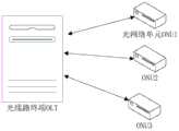
示例性地,本申请提供的光网络设备应用的通信系统可以如图1所示。其中,可以包括至少一个OLT,与至少一个ONU或至少一个ONT等。图1所包括的1个OLT与三个ONU(ONU1、ONU2、ONU3)仅仅是示例性说明,并不做限定。Exemplarily, the communication system applied by the optical network device provided in this application may be as shown in FIG. 1 . Wherein, at least one OLT, and at least one ONU or at least one ONT, etc. may be included. One OLT and three ONUs ( ONU1 , ONU2 , and ONU3 ) included in FIG. 1 are merely illustrative, and not limiting.
一个或多个ONU接入一个或多个OLT中。One or more ONUs are connected to one or more OLTs.
OLT是光接入网的核心部件,OLT用于为接入的一个或多个ONU提供数据,以及提供管理等等。The OLT is the core component of the optical access network, and the OLT is used to provide data and management for one or more ONUs that are accessed.
ONU用于接收OLT发送的数据,响应OLT的管理命令、对用户的以太网数据进行缓存,并在OLT分配的发送窗口中向上行方向发送等等。The ONU is used to receive the data sent by the OLT, respond to the management commands of the OLT, buffer the user's Ethernet data, and send it to the upstream direction in the sending window allocated by the OLT, and so on.
此外,OLT与ONU之间还可以包括光分配网络(optical distribution network,ODN),ODN(图中未示出)可以用于为OLT与ONU之间提供传输通道,还可以包括其他光网络设备等等,本申请对此并不做限定,具体可以根据实际应用场景进行调整。In addition, an optical distribution network (ODN) may also be included between the OLT and the ONU, and the ODN (not shown in the figure) may be used to provide a transmission channel between the OLT and the ONU, and may also include other optical network devices, etc. etc., which are not limited in this application, and can be adjusted according to actual application scenarios.
下面对本申请提供的PLC芯片进行介绍。The PLC chip provided by the present application will be introduced below.
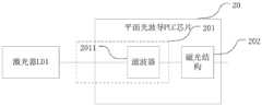
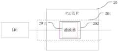
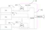
本申请提供的PLC芯片可以包括至少一条光传输通道,至少一条光传输通道中的至少一条光传输通道上设有滤波器。光传输通道的输入端接收激光器LD输入的光信号;滤波器用于滤除其所在光传输通道上的光信号中的功率低于阈值的部分;该PLC芯片还包括有磁光结构,该磁光结构用于隔离进入PLC芯片的反射光。The PLC chip provided by the present application may include at least one optical transmission channel, and at least one optical transmission channel in the at least one optical transmission channel is provided with a filter. The input end of the optical transmission channel receives the optical signal input by the laser LD; the filter is used to filter out the part of the optical signal on the optical transmission channel where the power is lower than the threshold value; the PLC chip also includes a magneto-optical structure, the magneto-optical The structure is used to isolate the reflected light entering the PLC chip.
其中,磁光结构可以由磁光材料组成,或者磁光结构可以是生长了磁光材料的结构。磁光结构可以通过多种方式实现,该磁光结构可以是覆盖在PLC芯片内的各个模块或部件上的结构,也可以是单独由磁光材料和光波导形成的结构。磁光材料可以隔离反射来的反射光。Wherein, the magneto-optical structure may be composed of a magneto-optical material, or the magneto-optical structure may be a structure in which a magneto-optical material is grown. The magneto-optical structure can be implemented in various ways. The magneto-optical structure can be a structure covered on each module or component in the PLC chip, or a structure formed by a magneto-optical material and an optical waveguide alone. The magneto-optical material can isolate the reflected light from the reflection.
以其中一条光传输通道为例,请参阅图2A以及图2B,请本申请提供的PLC芯片的结构示意图。Taking one of the optical transmission channels as an example, please refer to FIG. 2A and FIG. 2B for a schematic structural diagram of a PLC chip provided in this application.
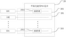
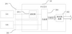
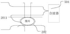
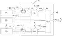
其中,PLC芯片可以包括光传输通道201以及磁光结构202,光传输通道201上设置有滤波器2011。The PLC chip may include an
光传输通道201的输入端接收来自LD1的光信号,滤波器2011可以滤除该光信号中功率低于阈值的部分。The input end of the
该光传输通道201的数量可以是一条或者多条。磁光结构可以设置于光传输通道上,也可以设置于PLC芯片的输出端。The number of the
如图2A所示,磁光结构可以是独立的部件,可以设置于滤波器2011的输出端。As shown in FIG. 2A , the magneto-optical structure may be an independent component and may be disposed at the output end of the
磁光结构也可以是覆盖或套设于PLC芯片内的各个部件的结构,磁光结构包括由磁光材料组成的结构,因此,也可以理解为在PLC芯片上生长了磁光材料。The magneto-optical structure can also be a structure covering or sheathing various components in the PLC chip. The magneto-optical structure includes a structure composed of magneto-optical materials. Therefore, it can also be understood that magneto-optical materials are grown on the PLC chip.
一种实现方式中,滤波器2011可以是具有啁啾管理功能的滤波器。该滤波器2011可以滤除光信号中功率低于阈值的部分,可以实现对光信号的啁啾管理。In one implementation, the
具体的,LD输出的光信号中,信号频率随时间变化,脉冲前后沿由于调制可能产生频率变化,使得光信号的频谱展宽。可以通过啁啾系数描述频谱的展宽,该啁啾系数也可以称为线宽展宽因子。频谱展宽可以线性的,也可以是非线性的。因此,可以使用具有啁啾管理功能的滤波器,滤除光信号中功率较低的部分,调整光信号的消光比,实现对光信号的啁啾管理。Specifically, in the optical signal output by the LD, the frequency of the signal changes with time, and the leading and trailing edges of the pulse may change in frequency due to modulation, which broadens the spectrum of the optical signal. The broadening of the spectrum can be described by a chirp coefficient, which can also be called a linewidth broadening factor. Spectral broadening can be linear or non-linear. Therefore, a filter with a chirp management function can be used to filter out the low-power part of the optical signal, adjust the extinction ratio of the optical signal, and realize the chirp management of the optical signal.
一种实现方式中,若光传输通道201上同时包括了滤波器2011以及磁光结构202,则可以对输入的光信号进行啁啾管理,则LD1可以是产生需要啁啾管理的光信号的激光器,也可以是产生不需要啁啾管理的光信号的激光器。例如,LD1可以是直接调制激光器(directly modulated laser,DML)或者电吸收调制激光器(Electro absorptionmodulated distributed feedback laser,EML)。通常,为提高PLC芯片内各个部件的有效利用率,LD1可以是DML,本申请提供的PLC芯片可以有效修复DML的消光比。In an implementation manner, if the
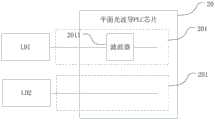
在前述图2A以及图2B所示的PLC芯片中,以一条光传输通道为例进行了说明,光传输通道的数量可以是一条或者多条,其中,至少有一条光传输通道上设置有滤波器。In the aforementioned PLC chips shown in FIG. 2A and FIG. 2B , an optical transmission channel is used as an example for description. The number of optical transmission channels may be one or more, and at least one optical transmission channel is provided with a filter. .
通常,某一条光传输通道接收EML输入的光信号,则该条通道上可以不设置滤波器,当然,也可以选择设置滤波器。Generally, if a certain optical transmission channel receives the optical signal input by the EML, the filter may not be set on this channel, and of course, the filter may also be set.
示例性地,以两条光传输通道为例,如图3所示,PLC芯片可以包括两条光传输通道201,以及磁光结构202(图中未示出),其中一条光传输通道201上设置了滤波器2011,以下称为第一光传输通道,另一条光传输通道201上未设置滤波器2011,以下称为第二光传输通道。Exemplarily, taking two optical transmission channels as an example, as shown in FIG. 3 , the PLC chip may include two
第一光传输通道接收LD1输入的光信号第二光传输通道接收LD2输入的光信号。The first optical transmission channel receives the optical signal input by the LD1, and the second optical transmission channel receives the optical signal input by the LD2.
通常,第一光传输通道上设置了可以进行啁啾管理的滤波器2011,而DML输出的光信号通常需要进行啁啾管理,因此,LD1可以是DML。当然,LD1也可以是EML。Generally, a
第二光传输上未设置滤波器,则无法对输入的光信号进行啁啾管理,因此,LD2可以是EML。If no filter is set on the second optical transmission, chirp management cannot be performed on the input optical signal, therefore, LD2 can be EML.
若PLC芯片包括多条光传输通道,如图4所示,则该多条光传输通道中,可以包括一条或多条第一光传输通道,以及一条或多条第二光传输通道。If the PLC chip includes multiple optical transmission channels, as shown in FIG. 4 , the multiple optical transmission channels may include one or more first optical transmission channels and one or more second optical transmission channels.
另一种实施方式中,若PLC芯片包括多条光传输通道,该多条光传输通道可以都为第一传输通道。In another embodiment, if the PLC chip includes multiple optical transmission channels, the multiple optical transmission channels may all be the first transmission channel.
因此,在本申请实施方式中,PLC芯片可以包括多条光传输通道,每条光传输通道上是否包括滤波器,可以根据对应的LD进行调整。若LD为消光比较差的LD,则对应的光传输通道可以设置滤波器,以修复该LD的消光比。若LD为消光比较优的LD,则对应的光传输通道也可以不设置滤波器,以降低PLC芯片的成本。因此,本申请实施方式提供的PLC芯片既可以适用于DML,也可以适用于EML。例如,若LD为成本较低的DML,则可以在对应的光传输通道设置滤波器,通过滤波器滤除低功率部分,对DML产生的光信号进行啁啾管理。Therefore, in the embodiments of the present application, the PLC chip may include multiple optical transmission channels, and whether each optical transmission channel includes a filter may be adjusted according to the corresponding LD. If the LD is an LD with poor extinction ratio, a filter can be set in the corresponding optical transmission channel to restore the extinction ratio of the LD. If the LD is an LD with better extinction, the corresponding optical transmission channel may not be provided with a filter to reduce the cost of the PLC chip. Therefore, the PLC chip provided by the embodiments of the present application may be applicable to both DML and EML. For example, if the LD is a low-cost DML, a filter can be set in the corresponding optical transmission channel, and the low-power part can be filtered out through the filter to perform chirp management on the optical signal generated by the DML.
通常,DML可以将电信号转换为光信号。而由于DML产生的光信号的啁啾量通常较大,因此可以在PLC芯片中增加具有啁啾管理的滤波器,用于对DML产生的光信号进行啁啾管理,滤除DML输出的光信号中的低功率部分,使后续接收端接收到合成的合波信号时,更易于识别或解码。In general, DML can convert electrical signals into optical signals. Since the chirp amount of the optical signal generated by the DML is usually large, a filter with chirp management can be added to the PLC chip to manage the chirp of the optical signal generated by the DML and filter out the optical signal output by the DML. The low-power part in the middle of the signal makes it easier to identify or decode when the subsequent receiving end receives the synthesized multiplexed signal.
在一种实施方式中,若PLC芯片仅包括一条光传输通道,则无需进行合波,进而无需设置合波器,可以降低成本。若PCL芯片上包括多条光传输通道,则需要对该多条光传输通道上传输的光信号进行合波,以下对包括了合波器的PLC芯片进行介绍。In one embodiment, if the PLC chip only includes one optical transmission channel, it is not necessary to perform multiplexing, and furthermore, there is no need to set a multiplexer, which can reduce the cost. If the PCL chip includes multiple optical transmission channels, it is necessary to combine the optical signals transmitted on the multiple optical transmission channels. The following describes the PLC chip including the multiplexer.
一种具体的实现方式中,PLC芯片中的光信号可以由光波导进行传输,PLC芯片可以包括光波导结构。示例性地,PLC芯片可以通过光波导接收LD产生的光信号,滤波器、合波器或其他器件之间也可以通过光波导连接。每条光传输通道中的光波导可以传输光信号,合波器的输出端的光波导可以输出合波信号等等,本申请以下实施例对PLC芯片所包括的光波导不再赘述。In a specific implementation manner, the optical signal in the PLC chip may be transmitted by an optical waveguide, and the PLC chip may include an optical waveguide structure. Exemplarily, the PLC chip can receive the optical signal generated by the LD through the optical waveguide, and the filter, the wave combiner or other devices can also be connected through the optical waveguide. The optical waveguides in each optical transmission channel can transmit optical signals, and the optical waveguides at the output end of the multiplexer can output multiplexed signals.
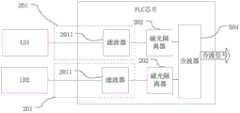
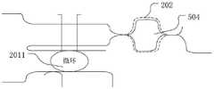
如图5所示,本申请实施例还提供了另一种PLC芯片。As shown in FIG. 5 , the embodiment of the present application further provides another PLC chip.
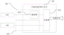
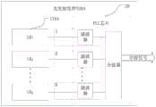
其中,PLC芯片除了可以包括多条光传输通道201以及磁光结构202(图5中未示出)之外,还可以包括合波器504。Wherein, the PLC chip may include a
其中,每条光传输通道201的输出端连接合波器的输入端。The output end of each
合波器504可以对输入的光信号进行合波,得到合波信号,然后经由合波器504的输出端输出该合波信号。The
本申请实施例中,可以在一条或多条光传输通道上设置滤波器,滤除LD输入的光信号中的低功率部分,以实现对光信号的啁啾管理。通过磁光结构实现对反射光的隔离。以及通过合波器对多条光传输通道上的光信号进行合波。因此,可以实现具有啁啾管理以及合波功能的非互易性PLC芯片。In the embodiment of the present application, a filter may be set on one or more optical transmission channels to filter out the low-power part of the optical signal input by the LD, so as to realize the chirp management of the optical signal. The isolation of reflected light is achieved by the magneto-optical structure. and multiplexing the optical signals on the multiple optical transmission channels through the multiplexer. Therefore, a non-reciprocal PLC chip with chirp management and multiplexing functions can be realized.
在一种可能的实现方式中,磁光结构生长在滤波器上。In one possible implementation, magneto-optical structures are grown on the filter.
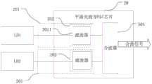
具体的,如图6所示,本申请实施例还提供了另一种PLC芯片。Specifically, as shown in FIG. 6 , the embodiment of the present application further provides another PLC chip.
在该PLC芯片中,磁光结构覆盖在一个或多个滤波器2011上。In this PLC chip, one or
磁光结构包括磁光材料形成的结构,或者,磁光结构由磁光材料组成。磁光结构可以是覆盖在滤波器上的磁光薄膜,也可以是其他与滤波器结构耦合的结构。The magneto-optical structure includes a structure formed of a magneto-optical material, or the magneto-optical structure is composed of a magneto-optical material. The magneto-optical structure can be a magneto-optical film covering the filter, or other structures coupled with the filter structure.
磁光材料可以使在滤波器上正向传输的光与反向传输的光之间相差半个自由光谱区(free spectral range,FSR),因此,反射光将无法通过滤波器,实现了对反射光的隔离。The magneto-optical material can make the difference between the light transmitted in the forward direction and the light transmitted in the reverse direction by half the free spectral range (FSR), so the reflected light will not be able to pass through the filter, and the reflection is realized. Light isolation.
在本申请实施方式中,可以在滤波器上生长磁光结构,可以滤除反射至滤波器的反射光。且滤波器又具有啁啾管理的功能,因此,本申请实施例提供的PLC芯片即具有反向隔离的功能,又具有啁啾管理的功能。且相对于单独的隔离器件,可以有效地减小PLC芯片的尺寸。In the embodiments of the present application, a magneto-optical structure can be grown on the filter, and the reflected light reflected to the filter can be filtered out. Moreover, the filter also has the function of chirp management. Therefore, the PLC chip provided by the embodiment of the present application has both the function of reverse isolation and the function of chirp management. And compared with a separate isolation device, the size of the PLC chip can be effectively reduced.
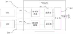
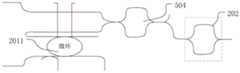
在另一种可能的实现方式中,磁光结构生长在合波器上。In another possible implementation, the magneto-optical structure is grown on the combiner.
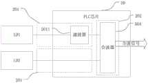
具体的,如图7所示,本申请实施例还提供了另一种PLC芯片。Specifically, as shown in FIG. 7 , the embodiment of the present application further provides another PLC chip.
在该PLC芯片中,磁光结构生长在合波器504上。In this PLC chip, the magneto-optical structure is grown on the
该磁光结构可以包括磁光材料形成的结构,或者,磁光结构由磁光材料组成。磁光结构可以是覆盖在滤波器上的磁光薄膜,也可以是其他与滤波器结构耦合的结构。The magneto-optical structure may include a structure formed of a magneto-optical material, or the magneto-optical structure is composed of a magneto-optical material. The magneto-optical structure can be a magneto-optical film covering the filter, or other structures coupled with the filter structure.
磁光结构覆盖在合波器上,可以使合波器上正向传输的光与反向传输的光之间相差半个FSR,因此,发射光不能通过合波器,可以实现对反射光的隔离。The magneto-optical structure is covered on the combiner, which can make the difference between the light transmitted in the forward direction and the light transmitted in the reverse direction on the combiner by half FSR. Therefore, the emitted light cannot pass through the combiner, and the reflected light can be separated. isolation.
在本申请实施方式中,可以在合波器上生长磁光结构,可以滤除反射至合波器的反射光。使得合波器即可以实现合波的功能,又可以实现对反射光的隔离。且相对于单独的隔离器件,可以有效地减小PLC芯片的尺寸。In the embodiments of the present application, the magneto-optical structure can be grown on the wave combiner, and the reflected light reflected to the wave combiner can be filtered out. So that the combiner can not only realize the function of combining waves, but also realize the isolation of reflected light. And compared with a separate isolation device, the size of the PLC chip can be effectively reduced.
在另一种可能的实现方式中,磁光结构为磁光隔离器。该磁光隔离器包括波导结构,该波导结构上生长了磁光材料。In another possible implementation manner, the magneto-optical structure is a magneto-optical isolator. The magneto-optical isolator includes a waveguide structure on which a magneto-optical material is grown.
具体的,请参阅图8,本申请实施例还提供了另一种PLC芯片。Specifically, referring to FIG. 8 , another PLC chip is further provided in the embodiment of the present application.
在该PLC芯片中,磁光结构可以是磁光隔离器,该磁光隔离器202包括生长了磁光材料的波导结构。In the PLC chip, the magneto-optical structure may be a magneto-optical isolator, and the magneto-
该磁光隔离器通过生在在波导上的磁光材料,滤除反射至磁光隔离器的发射光。The magneto-optical isolator filters out the emitted light reflected to the magneto-optical isolator through the magneto-optical material grown on the waveguide.
该磁光隔离器202可以设置在合波器的输出端。磁光隔离器202的输入端接收来自合波器的合波信号,然后输出该合波信号。The magneto-
磁光隔离器202的输出端可能接收外部的反射光,生长在磁光隔离器的波导上的磁光材料,使正向传输的合波信号与反射光之间相差半个FSR,可以使得反射光无法通过磁光隔离器202。The output end of the magneto-
在另一种可能的实现方式中,磁光隔离器202还可以设置于合波器的输入端。如图9所示,当磁光隔离器202设置于合波器的输入端时,可以是在每条光传输通道输出的光信号合路之前,在每条光传输通道的输出端设置磁光隔离器202,以实现对反射至每条光传输通道的反射光的隔离。In another possible implementation manner, the magneto-
在另一种可能的实现方式中,磁光隔离器202还可以设置于每条光传输通道的输入端与滤波器的输入端之间。可以理解为,如图10所示,磁光隔离器设置在LD之后,滤波器之前。磁光隔离器202可以正向接收来自LD的光信号,反向接收反射光。磁光隔离器中生长了磁光材料的波导结构,可以实现对反射至每条光传输通道的反射光的隔离。In another possible implementation manner, the magneto-
需要说明的是,以上在每条光传输通道上设置磁光隔离器的方式中,若某一条光传输通道上不包括滤波器,则该条光传输通道上可以设置磁光隔离器,也可以无需设置磁光隔离器。It should be noted that, in the above method of setting a magneto-optical isolator on each optical transmission channel, if a certain optical transmission channel does not include a filter, a magneto-optical isolator may be set on the optical transmission channel, or No magneto-optical isolator is required.
在本申请实施方式中,可以通过在波导结构上生长磁光材料,形成磁光隔离器,将该磁光隔离器设置在PLC芯片中,可以隔离反射光,可以避免反射光发射至激光器,而影响激光器的性能。相对于独立的空间型隔离器,在波导结构上生长磁光材料,无需较大体积的波导结构,即可对反射光进行隔离,可以降低PLC芯片的尺寸。In the embodiment of the present application, a magneto-optical isolator can be formed by growing a magneto-optical material on the waveguide structure, and the magneto-optical isolator can be arranged in the PLC chip, which can isolate the reflected light and prevent the reflected light from being emitted to the laser. affect the performance of the laser. Compared with the independent space-type isolator, the magneto-optical material is grown on the waveguide structure, and the reflected light can be isolated without a large-volume waveguide structure, which can reduce the size of the PLC chip.
在一些可能的实现方式中,前述的滤波器可以是具有啁啾管理功能的滤波器,例如,微环滤波器、光栅滤波器、马赫增德(Mach-Zehnder,MZ)型滤波器等等,具体可以根据实际应用场景进行调整,本申请对此不作限定。In some possible implementations, the aforementioned filter may be a filter with a chirp management function, for example, a micro-ring filter, a grating filter, a Mach-Zehnder (MZ) filter, etc., Specifically, it can be adjusted according to the actual application scenario, which is not limited in this application.
示例性地,在以下实施例中,以微环滤波器进行示例性说明,以下直接简称微环滤波器为微环。在实际应用中,也可以将该微环滤波器替换为光栅滤波器、MZ型滤波器等等具有滤波功能的器件。Exemplarily, in the following embodiments, a micro-ring filter is used for exemplary illustration, and the micro-ring filter is simply referred to as a micro-ring hereinafter. In practical applications, the micro-ring filter can also be replaced by a grating filter, an MZ-type filter, or other devices with filtering functions.
如图11所示,PLC芯片可以与至少一个LD(如图11所示的LD1、LD2…LDN)连接。PLC芯片上包括多N条光传输通道201,其中的一条或者多条光传输通道可以包括微环2011。PLC芯片还包括合波器504,N为大于1的正整数。As shown in FIG. 11 , the PLC chip can be connected with at least one LD (LD1 , LD2 . . . LDN shown in FIG. 11 ). The PLC chip includes a plurality of N
如图12所示,可以在微环2011上生长磁光材料,也可以理解为,磁光结构202为生长在微环上的磁光材料形成的结构。As shown in FIG. 12 , the magneto-optical material can be grown on the
以下称光从LD经微环至合波器的方向为正向,光从合波器至微环的方向为反向。Hereinafter, the direction of light from the LD through the micro-ring to the combiner is called forward, and the direction of light from the combiner to the micro-ring is reverse.
正向传输时,微环2011可以接入电流源,微环周期性地导通。当LD输出的光信号从微环的输入端输入时,微环2011导通,微环2011的输出端处于完全通光状态。而微环2011不导通时,微环2011处于不通光状态,不通过光信号。因此,可以通过微环滤波器对输入的光信号实现啁啾管理,调整光信号的前后沿,修复光信号的消光比。例如,通过微环可以滤除LD发送的激光信号中的“0”的功率,提升消光比,从而实现对激光信号的啁啾管理。During forward transmission, the micro-ring 2011 can be connected to a current source, and the micro-ring is periodically turned on. When the optical signal output by the LD is input from the input end of the microring, the
反向传输反射光时,由于磁光材料生长在微环2011上,使得微环的正向和反向的传播常数不同,使正向与反向相差半个FSR,因此,反射光并不能通过微环。When the reflected light is transmitted in the reverse direction, since the magneto-optical material grows on the
更具体地,在实际应用中,可以根据实际通过的光信号,调整微环的周期,以及调整磁光材料所覆盖的范围。从而调整正向和反向的传播常数,进而使正向通过的激光信号与反向的反射光相差半个FSR,即可使反射光不能通过微环。例如,若需要使正向与反向相差0.5个周期,那么,可以同时调整微环的导通周期,以及磁光材料所生长的范围,以调整正向和反向的常数。使得正向和反向传输相差0.5个周期。那么,在正向导通时,反向无法导通,进而隔离反射光,避免反射光通过微环,影响LD发射激光的性能。More specifically, in practical applications, the period of the microring can be adjusted and the range covered by the magneto-optical material can be adjusted according to the actual passing optical signal. Thus, the forward and reverse propagation constants are adjusted, so that the laser signal passing in the forward direction and the reflected light in the reverse direction differ by half FSR, so that the reflected light cannot pass through the microring. For example, if the difference between the forward and reverse directions needs to be 0.5 period, the conduction period of the microring and the growth range of the magneto-optical material can be adjusted at the same time to adjust the forward and reverse constants. Make the forward and reverse transmissions differ by 0.5 cycles. Then, during forward conduction, reverse conduction cannot be performed, thereby isolating the reflected light, preventing the reflected light from passing through the microring, and affecting the performance of the LD to emit laser light.
应理解,为了更详细地说明,图12中仅仅示出了一个完整的微环,PLC芯片包括的至少一个微环中的其他微环并未在图12中示出。It should be understood that, for a more detailed description, only one complete microring is shown in FIG. 12 , and other microrings in the at least one microring included in the PLC chip are not shown in FIG. 12 .
并且,在图12中,仅示出了一个LD与一个微环对应的场景,在实际应用中,一个LD可以与一个或多个微环连接,即一个LD的输出端可以串联或并联多个微环,具体的微环数量或连接方式可以通过实际应用场景进行调整,本申请实施例仅仅是示例性说明,并不做限定。Moreover, in Figure 12, only one LD corresponds to one micro-ring, in practical applications, one LD can be connected to one or more micro-rings, that is, the output of one LD can be connected in series or in parallel with multiple For microrings, the specific number or connection mode of microrings can be adjusted according to actual application scenarios, and the embodiments of the present application are merely illustrative, and not limiting.
因此,在本申请实施例中,PLC芯片中的微环生长了磁光材料,使得PLC芯片即具有啁啾管理和反向隔离的功能,又具有合波器的合波功能。并且,在不破坏原有微环的前提下,将微环与磁光材料集成在一起,可以实现具有隔离功能的非互易性滤波器件,可以有效地减小PLC芯片的尺寸,可以降低BOSA的封装成本以及封装复杂度,进而降低OLT的成本。Therefore, in the embodiment of the present application, the micro-ring in the PLC chip grows the magneto-optical material, so that the PLC chip has both the functions of chirp management and reverse isolation, and the wave combining function of the wave combiner. Moreover, on the premise of not destroying the original micro-ring, integrating the micro-ring and the magneto-optical material can realize a non-reciprocal filter device with isolation function, which can effectively reduce the size of the PLC chip and reduce the BOSA. The packaging cost and packaging complexity are reduced, thereby reducing the cost of the OLT.
在一些可能的实现方式中,前述的合波器可以是MZ型合波器、光栅干涉合波器、平行光波导合波器等等,具体可以根据实际应用场景进行调整,本申请对此不作限定。In some possible implementations, the aforementioned combiner may be an MZ-type combiner, a grating interference combiner, a parallel optical waveguide combiner, etc., which can be adjusted according to actual application scenarios, which are not discussed in this application. limited.
示例性地,在以下实施例中,以MZ型合波器为例进行说明。在实际应用中,也可以将该MZ型合波器替换为光栅干涉合波器、平行光波导合波器等等具有合波功能的器件。Exemplarily, in the following embodiments, an MZ-type combiner is taken as an example for description. In practical applications, the MZ-type multiplexer can also be replaced by a grating interference multiplexer, a parallel optical waveguide multiplexer, and other devices with multiplexing functions.
如图13所示,合波器504为MZ型合波器,合波器504上包括磁光结构202。磁光结构可以是磁光材料形成的结构,也可以理解为在MZ型合波器上生长了磁光材料。As shown in FIG. 13 , the
正向传输时,MZ型合波器的两臂的臂长不同,且MZ型合波器的两臂的臂长差值为预设值,该预设值具体可以根据实际通过的信号的波长或相位、反射光的波长或相位等等进行调整。两臂之间的相位差为2nπ+π/2,而磁光材料生长于MZ型合波器上,因磁光材料而使得合波器的光波导产生的相位差为-π/2,两臂的总相位差为2nπ,因此正向的啁啾信号与MZ型合波器形成干涉相长,正向导通。During forward transmission, the arm lengths of the two arms of the MZ-type combiner are different, and the difference between the arm lengths of the two arms of the MZ-type combiner is a preset value. or phase, wavelength or phase of reflected light, etc. The phase difference between the two arms is 2nπ+π/2, and the magneto-optical material is grown on the MZ-type multiplexer. Due to the magneto-optical material, the phase difference generated by the optical waveguide of the multiplexer is -π/2. The total phase difference of the arms is 2nπ, so the forward chirp signal and the MZ-type combiner form an interference constructive and forward conduction.
反向传输时,由于MZ型合波器的两臂的臂长之间的相位差为2nπ+π/2,而磁光材料生长于MZ型合波器上,因磁光材料而使得合波器的光波导的产生的相位差为π/2,因此,两臂总相位差为2nπ+π,使得反射光与MZ型合波器形成干涉相消,因此,反射光无法通过合波器,生长了磁光材料的合波器可以避免反射光通过合波器,对反射光形成隔离。该反射光为PBS分出的TM模式的波,或者PBS分出的TE模式的波经偏振旋转器转换后得到的TM模式的波。During reverse transmission, since the phase difference between the arm lengths of the two arms of the MZ-type multiplexer is 2nπ+π/2, and the magneto-optical material is grown on the MZ-type multiplexer, the combined wave is caused by the magneto-optical material. The phase difference generated by the optical waveguide of the device is π/2. Therefore, the total phase difference between the two arms is 2nπ+π, which makes the reflected light and the MZ-type combiner form interference cancellation. Therefore, the reflected light cannot pass through the combiner. The wavelength combiner grown with magneto-optical materials can prevent reflected light from passing through the wavelength combiner and isolate the reflected light. The reflected light is a TM mode wave branched by the PBS, or a TM mode wave obtained by converting the TE mode wave branched by the PBS after being converted by a polarization rotator.
具体地,MZ型合波器的两臂的臂长与磁光材料生长的范围可以结合进行调整,通常,可以根据公式:


因此,在本申请实施例中,PLC芯片中的合波器生长了磁光材料,使得PLC芯片即具有啁啾管理和反向隔离的功能,又具有合波器的合波功能。将合波器与磁光材料集成在一起,可以实现具有隔离功能的非互易性滤波器件,可以有效地减小PLC芯片的尺寸,可以降低BOSA的封装成本以及封装复杂度,进而降低OLT的成本。Therefore, in the embodiment of the present application, a magneto-optical material is grown on the wave combiner in the PLC chip, so that the PLC chip not only has the functions of chirp management and reverse isolation, but also has the wave combining function of the wave combiner. Integrating the multiplexer with the magneto-optical material can realize a non-reciprocal filter device with isolation function, which can effectively reduce the size of the PLC chip, reduce the packaging cost and packaging complexity of the BOSA, and further reduce the OLT. cost.
当然,除了可以将磁光材料生在于微环或者合波器中的任一种之外,也可以是微环与合波器上都生长磁光材料,具体可以根据实际应用场景调整,本申请对此并不做限定。Of course, in addition to the magneto-optical material that can be grown on either the microring or the wave combiner, the magneto-optical material can also be grown on both the microring and the wave combiner, which can be adjusted according to the actual application scenario. This is not limited.
在另一种实现方式中,磁光结构还可以是磁光隔离器。该磁光隔离器包括生长了磁光材料的波导结构。In another implementation manner, the magneto-optical structure may also be a magneto-optical isolator. The magneto-optical isolator includes a waveguide structure on which magneto-optical material is grown.
磁光隔离器中的波导结构可以是弯曲的形状,示例性地,以下实施例中以MZ型结构的磁光隔离器进行说明。在实际应用中,磁光隔离器可以包括各种弯曲形状的波导,且该波导上正在了磁光材料。The waveguide structure in the magneto-optical isolator may be in a curved shape, for example, a magneto-optical isolator with an MZ-type structure will be described in the following embodiments. In practical applications, the magneto-optical isolator may include waveguides with various curved shapes, and magneto-optical materials are placed on the waveguides.
如图14所示,PLC芯片可以包括微环滤波器2011、合波器504以及磁光隔离器202。As shown in FIG. 14 , the PLC chip may include a
其中,磁光隔离器202可以是MZ环形的波导结构,且该MZ环形的波导结构上生长了磁光材料。Wherein, the magneto-
与前述图13中的MZ型合波器隔离反射光的原理类似,此处不再赘述。The principle of isolating reflected light by the MZ-type wave combiner in the aforementioned FIG. 13 is similar, and details are not repeated here.
正向传输时,至少一个LD产生的激光信号可以经过至少一个微环进行啁啾管理,得到至少一个啁啾信号,然后由合波器对该至少一个啁啾信号进行合波,得到合波信号,然后经由磁光隔离器输出该合波信号。磁光隔离器可以输出合波信号,同时隔离反射进行磁光隔离器的反射光。During forward transmission, the laser signal generated by at least one LD can be managed by chirping through at least one microring to obtain at least one chirp signal, and then the at least one chirp signal is combined by the combiner to obtain the combined signal. , and then output the combined signal through the magneto-optical isolator. The magneto-optical isolator can output the combined wave signal, and at the same time isolate and reflect the reflected light of the magneto-optical isolator.
因此,在本申请实施例中,PLC芯片中的磁光隔离器生长了磁光材料,使得PLC芯片即具有啁啾管理和反向隔离的功能,又具有合波器的合波功能。将隔离器与磁光材料集成在一起,得到磁光隔离器,可以实现具有隔离功能的非互易性滤波器件。磁光隔离器在正向传输方向具有较低插入损耗,而对反向传输光有很大衰减作用,因此,可以隔离反射进PLC芯片的反射光。相对于空间型的隔离器,磁光隔离器可以有效地减小PLC芯片的尺寸和体积,可以降低BOSA的封装成本,进而降低OLT的成本。并且,相对于单独与PLC芯片耦合的空间型隔离器,本申请实施例提供的磁光隔离器,可以直接集成在PLC组件上,无需再次对PLC芯片与空间型隔离器进行封装,降低了TOSA、BOSA以及OLT的复杂度以及体积,降低光收发组件的成本,进一步降低空间型隔离器。Therefore, in the embodiment of the present application, the magneto-optical isolator in the PLC chip grows the magneto-optical material, so that the PLC chip not only has the functions of chirp management and reverse isolation, but also has the wave combining function of the wave combiner. The magneto-optical isolator is obtained by integrating the isolator and the magneto-optical material, and a non-reciprocal filter device with isolation function can be realized. The magneto-optical isolator has a low insertion loss in the forward transmission direction, and has a great attenuation effect on the reverse transmission light, so it can isolate the reflected light reflected into the PLC chip. Compared with space-type isolators, magneto-optical isolators can effectively reduce the size and volume of PLC chips, reduce the packaging cost of BOSA, and further reduce the cost of OLT. In addition, compared with the space-type isolator that is separately coupled with the PLC chip, the magneto-optical isolator provided by the embodiments of the present application can be directly integrated on the PLC component, and the PLC chip and the space-type isolator do not need to be packaged again, reducing TOSA. , BOSA and OLT complexity and volume, reduce the cost of optical transceiver components, and further reduce the space isolator.
需要说明的是,该磁光隔离器202除了可以设置与图14中合波器的输出端,还可以设置于合波器的输入端,当然,也可以同时设置在合波器的输入端与输出端,具体的设置位置可以根据实际应用场景进行调整,本申请实施例仅仅是示例性说明,并不作限定。It should be noted that the magneto-
在一种可能的实施方式中,前述的磁光材料或者磁光薄膜可以是磁光氧化物薄膜。该磁光氧化物薄膜可以生长于PLC芯片中。以隔离反射进PLC芯片的反射光。并且,相对于单独的空间型隔离器,本申请实施例提供的磁光氧化物薄膜可以降低PLC芯片的体积,无需另外耦合隔离器,降低了BOSA模块的封装复杂度以及体积,降低了BOSA模块的成本。In a possible implementation manner, the aforementioned magneto-optical material or magneto-optical film may be a magneto-optical oxide film. The magneto-optical oxide film can be grown in a PLC chip. In order to isolate the reflected light reflected into the PLC chip. Moreover, compared with a separate space-type isolator, the magneto-optical oxide film provided by the embodiment of the present application can reduce the volume of the PLC chip, without the need for additional coupling isolators, reducing the packaging complexity and volume of the BOSA module, and reducing the BOSA module. the cost of.
反射光可以分为横电波(transverse electric,TE)以及横磁波(TransverseMagnetic,TM),本申请提供的磁光结构所隔离的光为TM模式的光,因此,当存在TE模式的光时,还需要进一步隔离该TE模式的光。The reflected light can be divided into transverse electric (TE) and transverse magnetic (TM) waves. The light isolated by the magneto-optical structure provided in this application is light in TM mode. Therefore, when there is light in TE mode, This TE mode light needs to be further isolated.
在一种可能的实施方式中,可以在PLC芯片中设置偏振分束器(polarizationbeam splitter,PBS)以及弯曲光波导。PBS可以将反射光分为TE模式的光以及TM模式的光,TE模式的光可以经弯曲光波导损耗,TE模式的光可以由磁光结构隔离。In a possible implementation, a polarization beam splitter (PBS) and a curved optical waveguide may be provided in the PLC chip. The PBS can divide the reflected light into TE mode light and TM mode light. The TE mode light can be lost through the curved optical waveguide, and the TE mode light can be isolated by the magneto-optical structure.
在一些可能的实现方式中,PBS可以设置在合波器的输出端,当磁光结构设置在合波器的输入端时,PBS也可以设置在磁光结构与合波器的输入端之间。In some possible implementations, the PBS can be set at the output end of the wave combiner, and when the magneto-optical structure is set at the input end of the wave combiner, the PBS can also be set between the magneto-optical structure and the input end of the wave combiner .
示例性地,如图15所示,可以在PLC芯片中设置PBS1505以及弯曲光波导1506。PBS1505设置在合波器的输出端。PBS1505的第一端连接合波器的输出端,PBS1505的第二端输出合波信号,PBS1505的第三端连接弯曲光波导1506。Exemplarily, as shown in FIG. 15 , a
反射光从PBS1505的第二端输入至PBS,PBS1505对反射光进行分束,当反射光分束后得到TM模式的光时,将直接向合波器方向传输,通过合波器生长磁光材料、微环上生长磁光材料或者磁光隔离器,对TM模式的反射光进行隔离。当反射光分束后得到TE模式的光时,PBS1505将TE模式的光传输至弯曲光波导1506,TE模式的光经弯曲光波导后损耗,因此,实现对TE模式的反射光的隔离。The reflected light is input to the PBS from the second end of the PBS1505, and the PBS1505 splits the reflected light. When the reflected light is split and the TM mode light is obtained, it will be transmitted directly to the wave combiner, and the magneto-optical material will grow through the wave combiner. , Magneto-optical materials or magneto-optical isolators are grown on the microrings to isolate the reflected light in the TM mode. When the reflected light is split to obtain TE mode light, the
通常,PBS可以包括分光棱镜,TE模式波的电矢量垂直于入射面,TM模式波的电矢量在入射面内。In general, the PBS may include a beam splitter prism, the electric vector of the TE mode wave is perpendicular to the plane of incidence, and the electric vector of the TM mode wave is in the plane of incidence.
弯曲光波导1506可以是单独的一段弯曲形状的光波导,也可以是PLC芯片中弯曲形状的光波导。The curved
示例性地,一个或多个PBS1505设置在磁光结构与合波器之间。如图16所示,可以在PLC芯片中合波器的输入端设置一个或多个PBS1505以及一个或多个弯曲光波导1506。Illustratively, one or
其中,可以在具有滤波器的光传输通道中设置PBS1505以及弯曲光波导1506。而不具有滤波器的光传输通道,可以设置PBS1505,也可以不设置PBS1505,具体可以根据实际应用场景调整。Among them, the
任意一个PBS1505的第一端连接滤波器2011的输出端,PBS1505的第二端输出合波信号,PBS1505的第三端连接弯曲光波导1506。The first end of any PBS1505 is connected to the output end of the
反射光首先从PBS1505的第二端输入,PBS1505对反射光进行分束。当反射光为TM模式的波时,将直接向合波器方向传输,通过微环上生长磁光材料或者磁光隔离器,对TM模式的反射光进行隔离。当反射光分束后得到TE模式的光时,PBS1505将TE模式的光传输至弯曲光波导1506,TE模式的光经弯曲光波导后损耗,因此,实现对TE模式的反射光的隔离。The reflected light is first input from the second end of the PBS1505, and the PBS1505 splits the reflected light. When the reflected light is a wave in the TM mode, it will be transmitted directly to the wave combiner, and the reflected light in the TM mode is isolated by growing magneto-optical materials or magneto-optical isolators on the microring. When the reflected light is split to obtain TE mode light, the
在另一种实现方式中,除了可以通过第一弯曲光波导的方式消除TE模式的光外,也可以使使用偏振旋转器将TE模式的转换为TM模式的波,通过合波器生长磁光材料、微环上生长磁光材料或者磁光隔离器,对TM模式的反射光进行隔离。In another implementation, in addition to eliminating the TE mode light by means of the first curved optical waveguide, a polarization rotator can also be used to convert the TE mode into the TM mode wave, and the magneto-optical wave can be grown through a wave combiner A magneto-optical material or a magneto-optical isolator is grown on the material and the microring to isolate the reflected light in the TM mode.
在另一种实现方式中,也可以在合波器的输出端设置PBS,还可以同时在合波器与磁光结构之间设置PBS,以实现对反射更全面的转换,更全面地隔离反射光。In another implementation manner, a PBS can also be set at the output end of the combiner, and a PBS can also be set between the combiner and the magneto-optical structure at the same time, so as to realize a more comprehensive conversion of reflections and a more comprehensive isolation of reflections Light.
在一些可能的实现方式中,PLC芯片除了集成了微环与合波器之外,还可以集成其他的光器件,例如,分光器,本申请实施例对此并不作限定,不再一一进行具体说明。In some possible implementations, the PLC chip may integrate other optical devices, such as optical splitters, in addition to the microring and the wave combiner, which are not limited in the embodiments of the present application, and will not be performed one by one. Specific instructions.
前述对本申请提供的PLC芯片进行了详细说明,本申请还提供了一种TOSA、BOSA、光模块、以及光网络设备等等,下面分别进行说明。The PLC chip provided by the present application has been described in detail above. The present application also provides a TOSA, a BOSA, an optical module, and an optical network device, etc., which will be described separately below.
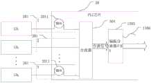
本申请实施例提供了一种TOSA,该TOSA可以包括至少一个LD以及前述图2A-16中任一项实施例中的PLC芯片,PLC芯片的具体结构请参阅前述图2A-16。An embodiment of the present application provides a TOSA, and the TOSA may include at least one LD and the PLC chip in any of the foregoing embodiments in FIGS. 2A-16 . For the specific structure of the PLC chip, please refer to the foregoing FIGS. 2A-16 .
示例性地,如图17所示,本申请还提供了一种TOSA。该TOSA可以包括PLC芯片20以及至少一个LD1701。Exemplarily, as shown in FIG. 17 , the present application also provides a TOSA. The TOSA may include the
至少一个LD701用于产生激光,得到光信号,并输入至PLC芯片20。At least one LD701 is used to generate laser light, obtain optical signals, and input them to the
PLC芯片20可以包括一条或多条光传输通道以及磁光结构。该一条或多条光传输通道中至少一条设置有滤波器。该磁光结构用于隔离反射光。The
当存在多条光传输通道时,该PLC芯片还包括合波器。该合波器用于对多条光传输通道上传输的光信号进行合波,得到合波信号。When there are multiple optical transmission channels, the PLC chip also includes a wave combiner. The multiplexer is used for multiplexing optical signals transmitted on multiple optical transmission channels to obtain multiplexed signals.
至少一个LD可以包括DML或者EML,当其中一个LD为DML时,PLC芯片中接收该LD产生的光信号的光传输通道中,设置有滤波器。当其中一个LD为EML时,PLC芯片中接收该LD产生的光信号的光传输通道中,可以设置滤波器,也可以不设置滤波器。At least one LD may include DML or EML, and when one of the LDs is DML, a filter is provided in the optical transmission channel in the PLC chip that receives the optical signal generated by the LD. When one of the LDs is an EML, a filter may or may not be set in the optical transmission channel in the PLC chip that receives the optical signal generated by the LD.
在本申请实施方式中,可以通过滤波器对LD产生的激光信号进行啁啾管理,并通过磁光结构对反射光进行隔离。可以实现具有啁啾管理的非互易性TOSA。并且,本申请实施例中的磁光结构为磁光材料形成的结构,相对于空间型隔离器,可以降低PLC芯片的尺寸以及复杂度,进而降低TOSA的尺寸以及复杂度。In the embodiment of the present application, the chirp management of the laser signal generated by the LD can be performed by the filter, and the reflected light can be isolated by the magneto-optical structure. A non-reciprocal TOSA with chirp management can be implemented. In addition, the magneto-optical structure in the embodiment of the present application is a structure formed of magneto-optical materials, which can reduce the size and complexity of the PLC chip compared with the space-type isolator, thereby reducing the size and complexity of the TOSA.
本申请实施例还提供了一种BOSA,该BOSA可以包括TOSA以及光接收组件(Receiver Optical Subassembly,ROSA)。An embodiment of the present application further provides a BOSA, where the BOSA may include a TOSA and an optical receiving assembly (Receiver Optical Subassembly, ROSA).
TOSA可以是本申请提供的TOSA,该TOSA包括前述图2A-16中任一实施方式中的PLC芯片。该TOSA可以用于发射光信号。The TOSA may be the TOSA provided in this application, and the TOSA includes the PLC chip in any of the foregoing embodiments in FIGS. 2A-16 . The TOSA can be used to transmit optical signals.
ROSA可以包括滤波器、波分复用器、透镜阵列、光接收PD阵列等等。ROSA可以用于接收光信号。ROSAs may include filters, wavelength division multiplexers, lens arrays, light receiving PD arrays, and the like. ROSA can be used to receive optical signals.
本申请实施例提供的BOSA可以包括前述图2A-16中任一项实施例中的PLC芯片,通过在PLC芯片中生长磁光结构的方式,隔离反射光。防止反射光影响LD的性能,减小了PLC芯片的体积,减小了BOSA的尺寸和复杂度,降低了BOSA的封装成本。The BOSA provided in this embodiment of the present application may include the PLC chip in any of the foregoing embodiments in FIGS. 2A-16 , and the reflected light is isolated by growing a magneto-optical structure in the PLC chip. Preventing reflected light from affecting the performance of the LD reduces the volume of the PLC chip, reduces the size and complexity of the BOSA, and reduces the packaging cost of the BOSA.
基于该BOSA,本申请实施例还提供了一种光模块。本申请提供的光模块可以包括该BOSA,以及其他的模块,例如发射电路、接收电路、控制电路等等。Based on the BOSA, an embodiment of the present application further provides an optical module. The optical module provided in this application may include the BOSA, and other modules, such as a transmitting circuit, a receiving circuit, a control circuit, and the like.
BOSA中可以包括前述图2A-16中任一项实施例中的PLC芯片,通过在PLC芯片中生长磁光结构的方式,隔离反射光。防止反射光影响LD的性能,减小了PLC芯片的体积,减小了BOSA的尺寸和复杂度,进而可以降低光模块的尺寸以及复杂度,降低光模块的成本。The BOSA may include the PLC chip in any of the foregoing embodiments in FIGS. 2A-16 , and the reflected light is isolated by growing a magneto-optical structure in the PLC chip. Preventing reflected light from affecting the performance of the LD reduces the size of the PLC chip, and reduces the size and complexity of the BOSA, thereby reducing the size and complexity of the optical module and reducing the cost of the optical module.
基于该光模块,本申请实施例还提供了一种光网络设备。该光网络设备可以包括一个或多个该光模块,还可以包括单板、控制电路等等,在不同的应用场景中所包括的部件可能不相同,本申请对此不再一一赘述。Based on the optical module, an embodiment of the present application further provides an optical network device. The optical network device may include one or more of the optical modules, and may also include a single board, a control circuit, etc., and the components included in different application scenarios may be different, which will not be repeated in this application.
例如,BOSA包括发射部分与接收部分,本申请提供的TOSA可以应用于BOSA的发射部分,而BOSA可以应用于光模块。例如,BOSA可以属于光组合(COMBO)单元或者密集型光波复用(Dense Wavelength Division Multiplexing,DWDM)单元。COMBO单元或DWDM单元可以应用于光网络设备。光网络设备可以包括OLT、ONU、ONT等具有光通信功能的网络设备。For example, a BOSA includes a transmitting part and a receiving part, the TOSA provided in this application can be applied to the transmitting part of the BOSA, and the BOSA can be applied to an optical module. For example, the BOSA may belong to a Combining Optical (COMBO) unit or a Dense Wavelength Division Multiplexing (DWDM) unit. COMBO units or DWDM units can be applied to optical network equipment. The optical network equipment may include network equipment with optical communication functions such as OLT, ONU, ONT, etc.
本申请的说明书和权利要求书及上述附图中的术语“第一”、“第二”、“第三”、“第四”等(如果存在)是用于区别类似的对象,而不必用于描述特定的顺序或先后次序。应该理解这样使用的数据在适当情况下可以互换,以便这里描述的实施例能够以除了在这里图示或描述的内容以外的顺序实施。此外,术语“包括”和“具有”以及他们的任何变形,意图在于覆盖不排他的包含,例如,包含了一系列步骤或单元的过程、方法、系统、产品或设备不必限于清楚地列出的那些步骤或单元,而是可包括没有清楚地列出的或对于这些过程、方法、产品或设备固有的其它步骤或单元。The terms "first", "second", "third", "fourth", etc. (if any) in the description and claims of this application and the above-mentioned drawings are used to distinguish similar objects and are not necessarily used to describe a specific order or sequence. It is to be understood that data so used may be interchanged under appropriate circumstances so that the embodiments described herein can be practiced in sequences other than those illustrated or described herein. Furthermore, the terms "comprising" and "having", and any variations thereof, are intended to cover non-exclusive inclusion, for example, a process, method, system, product or device comprising a series of steps or units is not necessarily limited to those expressly listed Rather, those steps or units may include other steps or units not expressly listed or inherent to these processes, methods, products or devices.
Claims (15)
Priority Applications (2)
| Application Number | Priority Date | Filing Date | Title |
|---|---|---|---|
| CN201910446404.6ACN111999801A (en) | 2019-05-27 | 2019-05-27 | PLC chip, TOSA, BOSA, optical module and optical network equipment |
| PCT/CN2020/074280WO2020238279A1 (en) | 2019-05-27 | 2020-02-04 | Plc chip, tosa, bosa, optical module, and optical network device |
Applications Claiming Priority (1)
| Application Number | Priority Date | Filing Date | Title |
|---|---|---|---|
| CN201910446404.6ACN111999801A (en) | 2019-05-27 | 2019-05-27 | PLC chip, TOSA, BOSA, optical module and optical network equipment |
Publications (1)
| Publication Number | Publication Date |
|---|---|
| CN111999801Atrue CN111999801A (en) | 2020-11-27 |
Family
ID=73461712
Family Applications (1)
| Application Number | Title | Priority Date | Filing Date |
|---|---|---|---|
| CN201910446404.6APendingCN111999801A (en) | 2019-05-27 | 2019-05-27 | PLC chip, TOSA, BOSA, optical module and optical network equipment |
Country Status (2)
| Country | Link |
|---|---|
| CN (1) | CN111999801A (en) |
| WO (1) | WO2020238279A1 (en) |
Cited By (1)
| Publication number | Priority date | Publication date | Assignee | Title |
|---|---|---|---|---|
| WO2024156213A1 (en)* | 2023-01-28 | 2024-08-02 | 中兴通讯股份有限公司 | Optical splitter of passive optical network and optical signal processing method |
Citations (9)
| Publication number | Priority date | Publication date | Assignee | Title |
|---|---|---|---|---|
| CN201051158Y (en)* | 2007-07-02 | 2008-04-23 | 深圳新飞通光电子技术有限公司 | PLC single fiber bidirectional three-port component |
| CN101672987A (en)* | 2008-09-12 | 2010-03-17 | 华为技术有限公司 | Optical isolator, optical add/drop multiplexer and optical combiner |
| CN102143407A (en)* | 2010-01-29 | 2011-08-03 | 华为技术有限公司 | Method, system and device for transmitting wavelength division multiplexing passive optical network |
| CN102674827A (en)* | 2012-05-28 | 2012-09-19 | 西安交通大学 | Novel integrated wave guide type optical isolator and preparation process thereof |
| WO2015024162A1 (en)* | 2013-08-19 | 2015-02-26 | 华为技术有限公司 | Optoisolator |
| CN106405755A (en)* | 2016-11-30 | 2017-02-15 | 武汉光迅科技股份有限公司 | High-speed multi-channel transmitting and receiving device |
| CN106461871A (en)* | 2014-03-31 | 2017-02-22 | 华为技术有限公司 | Apparatus and method for waveguide polarizer comprising series of bends |
| CN107153237A (en)* | 2017-06-20 | 2017-09-12 | 华中科技大学 | A kind of light transmit-receive integrated device of multichannel silicon substrate wavelength-division multiplex high speed |
| WO2018119791A1 (en)* | 2016-12-28 | 2018-07-05 | 华为技术有限公司 | Transmission optical assembly, optical device, optical module, and passive optical network system |
Family Cites Families (4)
| Publication number | Priority date | Publication date | Assignee | Title |
|---|---|---|---|---|
| US20090023237A1 (en)* | 2006-01-31 | 2009-01-22 | Tetsuya Mizumoto | Integrated optical isolator |
| US20170168252A1 (en)* | 2015-12-10 | 2017-06-15 | Kaiam Corp. | Optical transceiver with combined transmitter and receiver assembly |
| US20180059446A1 (en)* | 2016-08-29 | 2018-03-01 | Woosung Kim | Optical iso-modulator |
| CN109273974B (en)* | 2018-11-24 | 2024-01-05 | 光越科技(深圳)有限公司 | Wide-repetition-frequency adjustable high-power ultrashort pulse fiber laser |
- 2019
- 2019-05-27CNCN201910446404.6Apatent/CN111999801A/enactivePending
- 2020
- 2020-02-04WOPCT/CN2020/074280patent/WO2020238279A1/ennot_activeCeased
Patent Citations (9)
| Publication number | Priority date | Publication date | Assignee | Title |
|---|---|---|---|---|
| CN201051158Y (en)* | 2007-07-02 | 2008-04-23 | 深圳新飞通光电子技术有限公司 | PLC single fiber bidirectional three-port component |
| CN101672987A (en)* | 2008-09-12 | 2010-03-17 | 华为技术有限公司 | Optical isolator, optical add/drop multiplexer and optical combiner |
| CN102143407A (en)* | 2010-01-29 | 2011-08-03 | 华为技术有限公司 | Method, system and device for transmitting wavelength division multiplexing passive optical network |
| CN102674827A (en)* | 2012-05-28 | 2012-09-19 | 西安交通大学 | Novel integrated wave guide type optical isolator and preparation process thereof |
| WO2015024162A1 (en)* | 2013-08-19 | 2015-02-26 | 华为技术有限公司 | Optoisolator |
| CN106461871A (en)* | 2014-03-31 | 2017-02-22 | 华为技术有限公司 | Apparatus and method for waveguide polarizer comprising series of bends |
| CN106405755A (en)* | 2016-11-30 | 2017-02-15 | 武汉光迅科技股份有限公司 | High-speed multi-channel transmitting and receiving device |
| WO2018119791A1 (en)* | 2016-12-28 | 2018-07-05 | 华为技术有限公司 | Transmission optical assembly, optical device, optical module, and passive optical network system |
| CN107153237A (en)* | 2017-06-20 | 2017-09-12 | 华中科技大学 | A kind of light transmit-receive integrated device of multichannel silicon substrate wavelength-division multiplex high speed |
Cited By (1)
| Publication number | Priority date | Publication date | Assignee | Title |
|---|---|---|---|---|
| WO2024156213A1 (en)* | 2023-01-28 | 2024-08-02 | 中兴通讯股份有限公司 | Optical splitter of passive optical network and optical signal processing method |
Also Published As
| Publication number | Publication date |
|---|---|
| WO2020238279A1 (en) | 2020-12-03 |
Similar Documents
| Publication | Publication Date | Title |
|---|---|---|
| US20200012055A1 (en) | Bi-directional optical sub-assembly, optical network unit, optical line terminal, and passive optical network system | |
| KR101954376B1 (en) | Optical network communication system with optical line terminal transceiver and method of operation thereof | |
| US9448367B2 (en) | Multi-channel optical transceiver module including dual fiber type direct link adapter for optically coupling optical subassemblies in the transceiver module | |
| TWI496425B (en) | Optical transmitter | |
| US10355783B2 (en) | Optical-to-optical transceiver and methods of making and using the same | |
| EP2518915A2 (en) | Apparatus and method for controlling the lasing wavelength of a tunable laser, and wavelength division multiplexed passive optical network comprising same | |
| US20090010648A1 (en) | Methods and apparatus for upgrading passive optical networks | |
| EP2637266A1 (en) | External cavity laser and wavelength division multiplexing passive optical network system | |
| WO2014020618A1 (en) | External cavity fabry -perot laser | |
| EP2512043A1 (en) | Polarization stabilization scheme for un-cooled self-tuning cavity for colorless ultra broadband PON | |
| WO2014067047A1 (en) | Wavelength tunable laser, passive optical network system and device | |
| US20050286903A1 (en) | Protocol and line-rate transparent WDM passive optical network | |
| CN117956322A (en) | Laser with optical signal management capability | |
| WO2019140999A1 (en) | Wavelength division multiplexing optical transmission apparatus and system, and implementation method | |
| US10128970B2 (en) | Bandwidth adjustable optical module and system | |
| CN103747371B (en) | A kind of time-division wavelength-division mixed multiplexing passive optical network system | |
| EP3079274A1 (en) | Optical transmitter, transmission method, optical receiver and reception method | |
| US20130343765A1 (en) | Optical network system and method | |
| CN109716678B (en) | Transmitting optical assembly, optical device, optical module and passive optical network system | |
| WO2012106920A1 (en) | Optical module, burst transmission method thereof, laser and optical network system | |
| US10230486B2 (en) | Optical transceiver with common end module | |
| US6411413B1 (en) | Method and apparatus for performing dispersion compensation without a change in polarization and a transmitter incorporating same | |
| KR101500056B1 (en) | Reflective semiconductor optical amplifier for optical networks | |
| CN111999801A (en) | PLC chip, TOSA, BOSA, optical module and optical network equipment | |
| US20230275672A1 (en) | Electronic device and method for tuning wavelenth in optical network |
Legal Events
| Date | Code | Title | Description |
|---|---|---|---|
| PB01 | Publication | ||
| PB01 | Publication | ||
| SE01 | Entry into force of request for substantive examination | ||
| SE01 | Entry into force of request for substantive examination | ||
| RJ01 | Rejection of invention patent application after publication | Application publication date:20201127 | |
| RJ01 | Rejection of invention patent application after publication |