CN111989793A - Light-emitting device, light-emitting device, electronic equipment and lighting device - Google Patents
Light-emitting device, light-emitting device, electronic equipment and lighting deviceDownload PDFInfo
- Publication number
- CN111989793A CN111989793ACN201980026537.6ACN201980026537ACN111989793ACN 111989793 ACN111989793 ACN 111989793ACN 201980026537 ACN201980026537 ACN 201980026537ACN 111989793 ACN111989793 ACN 111989793A
- Authority
- CN
- China
- Prior art keywords
- light
- organic compound
- layer
- emitting device
- skeleton
- Prior art date
- Legal status (The legal status is an assumption and is not a legal conclusion. Google has not performed a legal analysis and makes no representation as to the accuracy of the status listed.)
- Pending
Links
Images


Classifications
- H—ELECTRICITY
- H10—SEMICONDUCTOR DEVICES; ELECTRIC SOLID-STATE DEVICES NOT OTHERWISE PROVIDED FOR
- H10K—ORGANIC ELECTRIC SOLID-STATE DEVICES
- H10K85/00—Organic materials used in the body or electrodes of devices covered by this subclass
- H10K85/60—Organic compounds having low molecular weight
- H10K85/649—Aromatic compounds comprising a hetero atom
- H10K85/657—Polycyclic condensed heteroaromatic hydrocarbons
- H—ELECTRICITY
- H10—SEMICONDUCTOR DEVICES; ELECTRIC SOLID-STATE DEVICES NOT OTHERWISE PROVIDED FOR
- H10K—ORGANIC ELECTRIC SOLID-STATE DEVICES
- H10K50/00—Organic light-emitting devices
- H10K50/10—OLEDs or polymer light-emitting diodes [PLED]
- H10K50/11—OLEDs or polymer light-emitting diodes [PLED] characterised by the electroluminescent [EL] layers
- H—ELECTRICITY
- H10—SEMICONDUCTOR DEVICES; ELECTRIC SOLID-STATE DEVICES NOT OTHERWISE PROVIDED FOR
- H10K—ORGANIC ELECTRIC SOLID-STATE DEVICES
- H10K50/00—Organic light-emitting devices
- H10K50/10—OLEDs or polymer light-emitting diodes [PLED]
- H10K50/14—Carrier transporting layers
- H10K50/15—Hole transporting layers
- H—ELECTRICITY
- H10—SEMICONDUCTOR DEVICES; ELECTRIC SOLID-STATE DEVICES NOT OTHERWISE PROVIDED FOR
- H10K—ORGANIC ELECTRIC SOLID-STATE DEVICES
- H10K50/00—Organic light-emitting devices
- H10K50/10—OLEDs or polymer light-emitting diodes [PLED]
- H10K50/14—Carrier transporting layers
- H10K50/16—Electron transporting layers
- H—ELECTRICITY
- H10—SEMICONDUCTOR DEVICES; ELECTRIC SOLID-STATE DEVICES NOT OTHERWISE PROVIDED FOR
- H10K—ORGANIC ELECTRIC SOLID-STATE DEVICES
- H10K50/00—Organic light-emitting devices
- H10K50/10—OLEDs or polymer light-emitting diodes [PLED]
- H10K50/17—Carrier injection layers
- H—ELECTRICITY
- H10—SEMICONDUCTOR DEVICES; ELECTRIC SOLID-STATE DEVICES NOT OTHERWISE PROVIDED FOR
- H10K—ORGANIC ELECTRIC SOLID-STATE DEVICES
- H10K85/00—Organic materials used in the body or electrodes of devices covered by this subclass
- H10K85/60—Organic compounds having low molecular weight
- H10K85/649—Aromatic compounds comprising a hetero atom
- H10K85/657—Polycyclic condensed heteroaromatic hydrocarbons
- H10K85/6572—Polycyclic condensed heteroaromatic hydrocarbons comprising only nitrogen in the heteroaromatic polycondensed ring system, e.g. phenanthroline or carbazole
- H—ELECTRICITY
- H10—SEMICONDUCTOR DEVICES; ELECTRIC SOLID-STATE DEVICES NOT OTHERWISE PROVIDED FOR
- H10K—ORGANIC ELECTRIC SOLID-STATE DEVICES
- H10K85/00—Organic materials used in the body or electrodes of devices covered by this subclass
- H10K85/60—Organic compounds having low molecular weight
- H10K85/649—Aromatic compounds comprising a hetero atom
- H10K85/657—Polycyclic condensed heteroaromatic hydrocarbons
- H10K85/6574—Polycyclic condensed heteroaromatic hydrocarbons comprising only oxygen in the heteroaromatic polycondensed ring system, e.g. cumarine dyes
- H—ELECTRICITY
- H10—SEMICONDUCTOR DEVICES; ELECTRIC SOLID-STATE DEVICES NOT OTHERWISE PROVIDED FOR
- H10K—ORGANIC ELECTRIC SOLID-STATE DEVICES
- H10K85/00—Organic materials used in the body or electrodes of devices covered by this subclass
- H10K85/60—Organic compounds having low molecular weight
- H10K85/649—Aromatic compounds comprising a hetero atom
- H10K85/657—Polycyclic condensed heteroaromatic hydrocarbons
- H10K85/6576—Polycyclic condensed heteroaromatic hydrocarbons comprising only sulfur in the heteroaromatic polycondensed ring system, e.g. benzothiophene
- H—ELECTRICITY
- H10—SEMICONDUCTOR DEVICES; ELECTRIC SOLID-STATE DEVICES NOT OTHERWISE PROVIDED FOR
- H10K—ORGANIC ELECTRIC SOLID-STATE DEVICES
- H10K2101/00—Properties of the organic materials covered by group H10K85/00
- H10K2101/10—Triplet emission
- H—ELECTRICITY
- H10—SEMICONDUCTOR DEVICES; ELECTRIC SOLID-STATE DEVICES NOT OTHERWISE PROVIDED FOR
- H10K—ORGANIC ELECTRIC SOLID-STATE DEVICES
- H10K2101/00—Properties of the organic materials covered by group H10K85/00
- H10K2101/20—Delayed fluorescence emission
- H—ELECTRICITY
- H10—SEMICONDUCTOR DEVICES; ELECTRIC SOLID-STATE DEVICES NOT OTHERWISE PROVIDED FOR
- H10K—ORGANIC ELECTRIC SOLID-STATE DEVICES
- H10K2101/00—Properties of the organic materials covered by group H10K85/00
- H10K2101/30—Highest occupied molecular orbital [HOMO], lowest unoccupied molecular orbital [LUMO] or Fermi energy values
- H—ELECTRICITY
- H10—SEMICONDUCTOR DEVICES; ELECTRIC SOLID-STATE DEVICES NOT OTHERWISE PROVIDED FOR
- H10K—ORGANIC ELECTRIC SOLID-STATE DEVICES
- H10K2101/00—Properties of the organic materials covered by group H10K85/00
- H10K2101/40—Interrelation of parameters between multiple constituent active layers or sublayers, e.g. HOMO values in adjacent layers
- H—ELECTRICITY
- H10—SEMICONDUCTOR DEVICES; ELECTRIC SOLID-STATE DEVICES NOT OTHERWISE PROVIDED FOR
- H10K—ORGANIC ELECTRIC SOLID-STATE DEVICES
- H10K2101/00—Properties of the organic materials covered by group H10K85/00
- H10K2101/90—Multiple hosts in the emissive layer
- H—ELECTRICITY
- H10—SEMICONDUCTOR DEVICES; ELECTRIC SOLID-STATE DEVICES NOT OTHERWISE PROVIDED FOR
- H10K—ORGANIC ELECTRIC SOLID-STATE DEVICES
- H10K59/00—Integrated devices, or assemblies of multiple devices, comprising at least one organic light-emitting element covered by group H10K50/00
- H10K59/80—Constructional details
- H10K59/875—Arrangements for extracting light from the devices
- H—ELECTRICITY
- H10—SEMICONDUCTOR DEVICES; ELECTRIC SOLID-STATE DEVICES NOT OTHERWISE PROVIDED FOR
- H10K—ORGANIC ELECTRIC SOLID-STATE DEVICES
- H10K85/00—Organic materials used in the body or electrodes of devices covered by this subclass
- H10K85/30—Coordination compounds
- H—ELECTRICITY
- H10—SEMICONDUCTOR DEVICES; ELECTRIC SOLID-STATE DEVICES NOT OTHERWISE PROVIDED FOR
- H10K—ORGANIC ELECTRIC SOLID-STATE DEVICES
- H10K85/00—Organic materials used in the body or electrodes of devices covered by this subclass
- H10K85/30—Coordination compounds
- H10K85/341—Transition metal complexes, e.g. Ru(II)polypyridine complexes
- H10K85/342—Transition metal complexes, e.g. Ru(II)polypyridine complexes comprising iridium
- H—ELECTRICITY
- H10—SEMICONDUCTOR DEVICES; ELECTRIC SOLID-STATE DEVICES NOT OTHERWISE PROVIDED FOR
- H10K—ORGANIC ELECTRIC SOLID-STATE DEVICES
- H10K85/00—Organic materials used in the body or electrodes of devices covered by this subclass
- H10K85/60—Organic compounds having low molecular weight
- H10K85/615—Polycyclic condensed aromatic hydrocarbons, e.g. anthracene
- H10K85/622—Polycyclic condensed aromatic hydrocarbons, e.g. anthracene containing four rings, e.g. pyrene
- H—ELECTRICITY
- H10—SEMICONDUCTOR DEVICES; ELECTRIC SOLID-STATE DEVICES NOT OTHERWISE PROVIDED FOR
- H10K—ORGANIC ELECTRIC SOLID-STATE DEVICES
- H10K85/00—Organic materials used in the body or electrodes of devices covered by this subclass
- H10K85/60—Organic compounds having low molecular weight
- H10K85/615—Polycyclic condensed aromatic hydrocarbons, e.g. anthracene
- H10K85/626—Polycyclic condensed aromatic hydrocarbons, e.g. anthracene containing more than one polycyclic condensed aromatic rings, e.g. bis-anthracene
- H—ELECTRICITY
- H10—SEMICONDUCTOR DEVICES; ELECTRIC SOLID-STATE DEVICES NOT OTHERWISE PROVIDED FOR
- H10K—ORGANIC ELECTRIC SOLID-STATE DEVICES
- H10K85/00—Organic materials used in the body or electrodes of devices covered by this subclass
- H10K85/60—Organic compounds having low molecular weight
- H10K85/631—Amine compounds having at least two aryl rest on at least one amine-nitrogen atom, e.g. triphenylamine
- H10K85/636—Amine compounds having at least two aryl rest on at least one amine-nitrogen atom, e.g. triphenylamine comprising heteroaromatic hydrocarbons as substituents on the nitrogen atom
Landscapes
- Physics & Mathematics (AREA)
- Spectroscopy & Molecular Physics (AREA)
- Chemical & Material Sciences (AREA)
- Engineering & Computer Science (AREA)
- Materials Engineering (AREA)
- Optics & Photonics (AREA)
- Electroluminescent Light Sources (AREA)
- Led Device Packages (AREA)
- Illuminated Signs And Luminous Advertising (AREA)
Abstract
Description
Translated fromChinese技术领域technical field
本发明的一个实施方式涉及一种发光元件、发光器件、显示模块、照明模块、显示装置、发光装置、电子设备及照明装置。注意,本发明的一个实施方式不局限于上述技术领域。本说明书等所公开的发明的一个实施方式的技术领域涉及一种物体、方法或制造方法。本发明的一个实施方式涉及一种程序(process)、机器(machine)、产品(manufacture)或者组合物(composition of matter)。具体而言,作为本说明书所公开的本发明的一个实施方式的技术领域的例子,可以举出半导体装置、显示装置、液晶显示装置、发光装置、照明装置、蓄电装置、存储装置、摄像装置、它们的驱动方法以及它们的制造方法。One embodiment of the present invention relates to a light-emitting element, a light-emitting device, a display module, a lighting module, a display device, a light-emitting device, an electronic device, and a lighting device. Note that one embodiment of the present invention is not limited to the above technical field. The technical field of one embodiment of the invention disclosed in this specification and the like relates to an object, a method, or a manufacturing method. One embodiment of the invention relates to a process, machine, manufacture or composition of matter. Specifically, examples of the technical field of an embodiment of the present invention disclosed in this specification include a semiconductor device, a display device, a liquid crystal display device, a light-emitting device, a lighting device, a power storage device, a storage device, and an imaging device. , their driving method and their manufacturing method.
背景技术Background technique
近年来,使用有机化合物且利用电致发光(EL:Electroluminescence)的发光器件(有机EL器件)的实用化非常活跃。在这些发光器件的基本结构中,在一对电极之间夹有包含发光材料的有机化合物层(EL层)。通过对该元件施加电压,注入载流子,利用该载流子的复合能量,可以获得来自发光材料的发光。In recent years, the practical application of light-emitting devices (organic EL devices) using electroluminescence (EL: Electroluminescence) using organic compounds has been very active. In the basic structure of these light-emitting devices, an organic compound layer (EL layer) containing a light-emitting material is sandwiched between a pair of electrodes. By applying a voltage to the element, carriers are injected, and light emission from the light-emitting material can be obtained by utilizing the recombination energy of the carriers.
因为这种发光器件是自发光型发光器件,所以当用于显示器的像素时比起液晶有可见度更高、不需要背光源等优势。另外,使用这种发光器件的显示器可以被制造成薄且轻,这也是极大的优点。再者,非常高速的响应也是该发光器件的特征之一。Because this light-emitting device is a self-luminous light-emitting device, it has advantages such as higher visibility and no need for a backlight when used in a pixel of a display. In addition, a display using such a light emitting device can be made thin and light, which is also a great advantage. Furthermore, a very high-speed response is also one of the characteristics of the light-emitting device.
因为这种发光器件的发光层可以在二维上连续地形成,所以可以获得面发光。这是在以白炽灯及LED为代表的点光源或者以荧光灯为代表的线光源中难以得到的特征。所以,作为可应用于照明等的面光源,上述发光器件的利用价值也高。Since the light-emitting layers of such a light-emitting device can be continuously formed two-dimensionally, surface light emission can be obtained. This is a feature that is difficult to obtain in point light sources represented by incandescent lamps and LEDs or line light sources represented by fluorescent lamps. Therefore, the above-mentioned light-emitting device is also highly useful as a surface light source that can be applied to lighting or the like.
如上所述,使用发光器件的显示器或照明装置适用于各种各样的电子设备,为了追求具有更良好的效率或寿命的发光器件的研究开发日益活跃。As described above, displays and lighting devices using light-emitting devices are suitable for various electronic devices, and research and development in pursuit of light-emitting devices having better efficiency and lifespan are increasingly active.
专利文献1公开了在接触于空穴注入层的第一空穴传输层与发光层之间设置其HOMO能级介于第一空穴注入层的HOMO能级与主体材料的HOMO能级之间的空穴传输材料的结构。
发光器件的特性明显得到了提高,但是还不足以对应对效率和耐久性等各种特性的高度要求。The characteristics of light-emitting devices have been significantly improved, but they are not sufficient to meet high demands for various characteristics such as efficiency and durability.
[参考文献][references]
[专利文献][Patent Literature]
[专利文献1]国际公开第2011/065136号小册子[Patent Document 1] International Publication No. 2011/065136 Pamphlet
发明内容SUMMARY OF THE INVENTION
本发明的一个实施方式的目的之一是提供一种新颖的发光器件。本发明的一个实施方式的另一目的是提供一种发光效率良好的发光器件。本发明的一个实施方式的另一目的是提供一种寿命良好的发光器件。本发明的一个实施方式的另一目的是提供一种驱动电压低的发光器件。One of the objectives of an embodiment of the present invention is to provide a novel light emitting device. Another object of one embodiment of the present invention is to provide a light-emitting device with good luminous efficiency. Another object of one embodiment of the present invention is to provide a light emitting device with a good lifetime. Another object of an embodiment of the present invention is to provide a light emitting device with a low driving voltage.
本发明的一个实施方式的另一目的是提供一种可靠性高的发光装置、电子设备及显示装置。本发明的一个实施方式的另一目的是提供一种功耗低的发光装置、电子设备及显示装置。Another object of an embodiment of the present invention is to provide a light-emitting device, an electronic device, and a display device with high reliability. Another object of an embodiment of the present invention is to provide a light-emitting device, an electronic device and a display device with low power consumption.
本发明只要实现上述目的中的任一个即可。The present invention should just achieve any one of the above-mentioned objects.
本发明的一个实施方式是一种发光器件,包括阳极、阴极、位于所述阳极与所述阴极间的EL层。所述EL层包括发光层。示出当向所述发光器件提供恒定电流时获得的发光亮度变化的劣化曲线具有极大值。One embodiment of the present invention is a light emitting device including an anode, a cathode, and an EL layer between the anode and the cathode. The EL layer includes a light-emitting layer. A degradation curve showing a change in light emission luminance obtained when a constant current is supplied to the light emitting device has a maximum value.
本发明的另一个实施方式是一种发光器件,包括阳极、阴极、位于所述阳极与所述阴极间的EL层。所述EL层从阳极侧依次包括第一层、第二层、第三层、发光层和第四层。所述第一层与所述阳极接触,并且所述第一层包含第一有机化合物和第二有机化合物。所述第二层包含第三有机化合物。所述第三层包含第四有机化合物。所述发光层包含第五有机化合物和第六有机化合物。所述第四层包含第七有机化合物。所述第一有机化合物是对所述第二有机化合物呈现电子接受性的有机化合物。所述第五有机化合物是发光中心物质。所述第二有机化合物的HOMO能级为-5.7eV以上且-5.4eV以下。所述第七有机化合物在电场强度[V/cm]的平方根为600时的电子迁移率为1×10-7cm2/Vs以上且5×10-5cm2/Vs以下。示出当向所述发光器件提供恒定电流时获得的发光亮度变化的劣化曲线具有极大值。Another embodiment of the present invention is a light emitting device including an anode, a cathode, and an EL layer between the anode and the cathode. The EL layer includes a first layer, a second layer, a third layer, a light emitting layer and a fourth layer in order from the anode side. The first layer is in contact with the anode, and the first layer includes a first organic compound and a second organic compound. The second layer includes a third organic compound. The third layer includes a fourth organic compound. The light-emitting layer includes a fifth organic compound and a sixth organic compound. The fourth layer includes a seventh organic compound. The first organic compound is an organic compound that exhibits electron acceptability to the second organic compound. The fifth organic compound is a luminescent center substance. The HOMO energy level of the second organic compound is -5.7 eV or more and -5.4 eV or less. The electron mobility of the seventh organic compound when the square root of the electric field intensity [V/cm] is 600 is 1×10⁻⁷ cm2 /Vs or more and 5×10⁻⁵ cm2 /Vs or less. A degradation curve showing a change in light emission luminance obtained when a constant current is supplied to the light emitting device has a maximum value.
本发明的另一个实施方式是一种发光器件,包括阳极、阴极以及所述阳极与所述阴极之间的EL层。所述EL层从阳极一侧依次包括第一层、第二层、第三层、发光层、第四层。所述第一层与所述阳极接触。所述第四层与所述发光层接触。所述第一层包含第一有机化合物及第二有机化合物。所述第二层包含第三有机化合物。所述第三层包含第四有机化合物。所述发光层包含第五有机化合物及第六有机化合物。所述第四层包含第七有机化合物。所述第一有机化合物为对所述第二有机化合物呈现电子接受性的有机化合物。所述第五有机化合物为发光中心物质。所述第二有机化合物的HOMO能级为-5.7eV以上且-5.4eV以下。所述第七有机化合物在电场强度[V/cm]的平方根为600时的电子迁移率为1×10-7cm2/Vs以上且5×10-5cm2/Vs以下。所述第七有机化合物的HOMO能级为-6.0eV以上。示出当向所述发光器件提供恒定电流时获得的发光亮度变化的劣化曲线具有极大值。Another embodiment of the present invention is a light emitting device including an anode, a cathode, and an EL layer between the anode and the cathode. The EL layer sequentially includes a first layer, a second layer, a third layer, a light-emitting layer, and a fourth layer from the anode side. The first layer is in contact with the anode. The fourth layer is in contact with the light emitting layer. The first layer includes a first organic compound and a second organic compound. The second layer includes a third organic compound. The third layer includes a fourth organic compound. The light-emitting layer includes a fifth organic compound and a sixth organic compound. The fourth layer includes a seventh organic compound. The first organic compound is an organic compound that exhibits electron acceptability to the second organic compound. The fifth organic compound is a luminescent center substance. The HOMO energy level of the second organic compound is -5.7 eV or more and -5.4 eV or less. The electron mobility of the seventh organic compound when the square root of the electric field intensity [V/cm] is 600 is 1×10⁻⁷ cm2 /Vs or more and 5×10⁻⁵ cm2 /Vs or less. The HOMO energy level of the seventh organic compound is -6.0 eV or more. A degradation curve showing a change in light emission luminance obtained when a constant current is supplied to the light emitting device has a maximum value.
本发明的另一个实施方式是一种发光器件,包括阳极、阴极以及所述阳极与所述阴极之间的EL层。所述EL层从阳极一侧依次包括第一层、第二层、第三层、发光层、第四层。所述第一层与所述阳极接触。所述第四层与所述发光层接触。所述第一层包含第一有机化合物及第二有机化合物。所述第二层包含第三有机化合物。所述第三层包含第四有机化合物。所述发光层包含第五有机化合物及第六有机化合物。所述第四层包含第七有机化合物。所述第一有机化合物为对所述第二有机化合物呈现电子接受性的有机化合物。所述第五有机化合物为发光中心物质。所述第二有机化合物的HOMO能级为-5.7eV以上且-5.4eV以下。所述第三有机化合物与所述第二有机化合物的HOMO能级差为0.2eV以下。所述第三有机化合物的HOMO能级与所述第二有机化合物的HOMO能级相同或更深。所述第七有机化合物在电场强度[V/cm]的平方根为600时的电子迁移率为1×10-7cm2/Vs以上且5×10-5cm2/Vs以下。所述第七有机化合物的HOMO能级为-6.0eV以上。示出当向所述发光器件提供恒定电流时获得的发光亮度变化的劣化曲线具有极大值。Another embodiment of the present invention is a light emitting device including an anode, a cathode, and an EL layer between the anode and the cathode. The EL layer sequentially includes a first layer, a second layer, a third layer, a light-emitting layer, and a fourth layer from the anode side. The first layer is in contact with the anode. The fourth layer is in contact with the light emitting layer. The first layer includes a first organic compound and a second organic compound. The second layer includes a third organic compound. The third layer includes a fourth organic compound. The light-emitting layer includes a fifth organic compound and a sixth organic compound. The fourth layer includes a seventh organic compound. The first organic compound is an organic compound that exhibits electron acceptability to the second organic compound. The fifth organic compound is a luminescent center substance. The HOMO energy level of the second organic compound is -5.7 eV or more and -5.4 eV or less. The HOMO level difference between the third organic compound and the second organic compound is 0.2 eV or less. The HOMO energy level of the third organic compound is the same as or deeper than the HOMO energy level of the second organic compound. The electron mobility of the seventh organic compound when the square root of the electric field intensity [V/cm] is 600 is 1×10⁻⁷ cm2 /Vs or more and 5×10⁻⁵ cm2 /Vs or less. The HOMO energy level of the seventh organic compound is -6.0 eV or more. A degradation curve showing a change in light emission luminance obtained when a constant current is supplied to the light emitting device has a maximum value.
本发明的另一个实施方式是一种发光器件,包括阳极、阴极以及所述阳极与所述阴极之间的EL层。所述EL层从阳极一侧依次包括第一层、第二层、第三层、发光层、第四层。所述第一层与所述阳极接触。所述第四层与所述发光层接触。所述第一层包含第一有机化合物及第二有机化合物。所述第二层包含第三有机化合物。所述第三层包含第四有机化合物。所述发光层包含第五有机化合物及第六有机化合物。所述第四层包含第七有机化合物。所述第一有机化合物为对所述第二有机化合物呈现电子接受性的有机化合物。所述第二有机化合物包含第一空穴传输性骨架。所述第三有机化合物包含第二空穴传输性骨架。所述第四有机化合物包含第三空穴传输性骨架。所述第五有机化合物为发光中心物质。所述第二有机化合物的HOMO能级为-5.7eV以上且-5.4eV以下。所述第一空穴传输性骨架、所述第二空穴传输性骨架及所述第三空穴传输性骨架分别独立为咔唑骨架、二苯并呋喃骨架、二苯并噻吩骨架和蒽骨架中的任一个。所述第七有机化合物在电场强度[V/cm]的平方根为600时的电子迁移率为1×10-7cm2/Vs以上且5×10-5cm2/Vs以下。所述第七有机化合物的HOMO能级为-6.0eV以上。示出当向所述发光器件提供恒定电流时获得的发光亮度变化的劣化曲线具有极大值。Another embodiment of the present invention is a light emitting device including an anode, a cathode, and an EL layer between the anode and the cathode. The EL layer sequentially includes a first layer, a second layer, a third layer, a light-emitting layer, and a fourth layer from the anode side. The first layer is in contact with the anode. The fourth layer is in contact with the light emitting layer. The first layer includes a first organic compound and a second organic compound. The second layer includes a third organic compound. The third layer includes a fourth organic compound. The light-emitting layer includes a fifth organic compound and a sixth organic compound. The fourth layer includes a seventh organic compound. The first organic compound is an organic compound that exhibits electron acceptability to the second organic compound. The second organic compound includes a first hole-transporting skeleton. The third organic compound includes a second hole-transporting skeleton. The fourth organic compound includes a third hole-transporting skeleton. The fifth organic compound is a luminescent center substance. The HOMO energy level of the second organic compound is -5.7 eV or more and -5.4 eV or less. The first hole-transporting skeleton, the second hole-transporting skeleton, and the third hole-transporting skeleton are independently a carbazole skeleton, a dibenzofuran skeleton, a dibenzothiophene skeleton, and an anthracene skeleton, respectively. any of the. The electron mobility of the seventh organic compound when the square root of the electric field intensity [V/cm] is 600 is 1×10⁻⁷ cm2 /Vs or more and 5×10⁻⁵ cm2 /Vs or less. The HOMO energy level of the seventh organic compound is -6.0 eV or more. A degradation curve showing a change in light emission luminance obtained when a constant current is supplied to the light emitting device has a maximum value.
本发明的另一个实施方式是一种发光器件,包括阳极、阴极以及所述阳极与所述阴极之间的EL层。所述EL层从阳极一侧依次包括第一层、第二层、第三层、发光层、第四层。所述第一层与所述阳极接触。所述第四层与所述发光层接触。所述第一层包含第一有机化合物及第二有机化合物。所述第二层包含第三有机化合物。所述第三层包含第四有机化合物。所述发光层包含第五有机化合物及第六有机化合物。所述第四层包含第七有机化合物和第八物质。所述第一有机化合物为对所述第二有机化合物呈现电子接受性的有机化合物。所述第五有机化合物为发光中心物质。所述第二有机化合物的HOMO能级为-5.7eV以上且-5.4eV以下。所述第七有机化合物是具有蒽骨架的有机化合物。所述第八物质是碱金属或碱土金属的有机配合物。示出当向所述发光器件提供恒定电流时获得的发光亮度变化的劣化曲线具有极大值。Another embodiment of the present invention is a light emitting device including an anode, a cathode, and an EL layer between the anode and the cathode. The EL layer sequentially includes a first layer, a second layer, a third layer, a light-emitting layer, and a fourth layer from the anode side. The first layer is in contact with the anode. The fourth layer is in contact with the light emitting layer. The first layer includes a first organic compound and a second organic compound. The second layer includes a third organic compound. The third layer includes a fourth organic compound. The light-emitting layer includes a fifth organic compound and a sixth organic compound. The fourth layer includes a seventh organic compound and an eighth substance. The first organic compound is an organic compound that exhibits electron acceptability to the second organic compound. The fifth organic compound is a luminescent center substance. The HOMO energy level of the second organic compound is -5.7 eV or more and -5.4 eV or less. The seventh organic compound is an organic compound having an anthracene skeleton. The eighth substance is an organic complex of an alkali metal or an alkaline earth metal. A degradation curve showing a change in light emission luminance obtained when a constant current is supplied to the light emitting device has a maximum value.
本发明的另一个实施方式是一种发光器件,包括阳极、阴极以及所述阳极与所述阴极之间的EL层。所述EL层从阳极一侧依次包括第一层、第二层、第三层、发光层、第四层。所述第一层与所述阳极接触。所述第四层与所述发光层接触。所述第一层包含第一有机化合物及第二有机化合物。所述第二层包含第三有机化合物。所述第三层包含第四有机化合物。所述发光层包含第五有机化合物及第六有机化合物。所述第四层包含第七有机化合物和第八物质。所述第一有机化合物为对所述第二有机化合物呈现电子接受性的有机化合物。所述第五有机化合物为发光中心物质。所述第二有机化合物的HOMO能级为-5.7eV以上且-5.4eV以下。所述第三有机化合物与所述第二有机化合物的HOMO能级差为0.2eV以下。所述第三有机化合物的HOMO能级与所述第二有机化合物的HOMO能级相同或更深。所述第七有机化合物是具有蒽骨架的有机化合物。所述第八物质是碱金属或碱土金属的有机配合物。示出当向所述发光器件提供恒定电流时获得的发光亮度变化的劣化曲线具有极大值。Another embodiment of the present invention is a light emitting device including an anode, a cathode, and an EL layer between the anode and the cathode. The EL layer sequentially includes a first layer, a second layer, a third layer, a light-emitting layer, and a fourth layer from the anode side. The first layer is in contact with the anode. The fourth layer is in contact with the light emitting layer. The first layer includes a first organic compound and a second organic compound. The second layer includes a third organic compound. The third layer includes a fourth organic compound. The light-emitting layer includes a fifth organic compound and a sixth organic compound. The fourth layer includes a seventh organic compound and an eighth substance. The first organic compound is an organic compound that exhibits electron acceptability to the second organic compound. The fifth organic compound is a luminescent center substance. The HOMO energy level of the second organic compound is -5.7 eV or more and -5.4 eV or less. The HOMO level difference between the third organic compound and the second organic compound is 0.2 eV or less. The HOMO energy level of the third organic compound is the same as or deeper than the HOMO energy level of the second organic compound. The seventh organic compound is an organic compound having an anthracene skeleton. The eighth substance is an organic complex of an alkali metal or an alkaline earth metal. A degradation curve showing a change in light emission luminance obtained when a constant current is supplied to the light emitting device has a maximum value.
本发明的另一个实施方式是一种发光器件,包括阳极、阴极以及所述阳极与所述阴极之间的EL层。所述EL层从阳极一侧依次包括第一层、第二层、第三层、发光层、第四层。所述第一层与所述阳极接触。所述第四层与所述发光层接触。所述第一层包含第一有机化合物及第二有机化合物。所述第二层包含第三有机化合物。所述第三层包含第四有机化合物。所述发光层包含第五有机化合物及第六有机化合物。所述第四层包含第七有机化合物及第八物质。所述第一有机化合物为对所述第二有机化合物呈现电子接受性的有机化合物。所述第二有机化合物包含第一空穴传输性骨架。所述第三有机化合物包含第二空穴传输性骨架。所述第四有机化合物包含第三空穴传输性骨架。所述第五有机化合物为发光中心物质。所述第二有机化合物的HOMO能级为-5.7eV以上且-5.4eV以下。所述第一空穴传输性骨架、所述第二空穴传输性骨架及所述第三空穴传输性骨架分别独立为咔唑骨架、二苯并呋喃骨架、二苯并噻吩骨架和蒽骨架中的任一个。所述第七有机化合物是具有蒽骨架的有机化合物。所述第八物质是碱金属或碱土金属的有机配合物。并且。示出当向所述发光器件提供恒定电流时获得的发光亮度变化的劣化曲线具有极大值。Another embodiment of the present invention is a light emitting device including an anode, a cathode, and an EL layer between the anode and the cathode. The EL layer sequentially includes a first layer, a second layer, a third layer, a light-emitting layer, and a fourth layer from the anode side. The first layer is in contact with the anode. The fourth layer is in contact with the light emitting layer. The first layer includes a first organic compound and a second organic compound. The second layer includes a third organic compound. The third layer includes a fourth organic compound. The light-emitting layer includes a fifth organic compound and a sixth organic compound. The fourth layer includes a seventh organic compound and an eighth substance. The first organic compound is an organic compound that exhibits electron acceptability to the second organic compound. The second organic compound includes a first hole-transporting skeleton. The third organic compound includes a second hole-transporting skeleton. The fourth organic compound includes a third hole-transporting skeleton. The fifth organic compound is a luminescent center substance. The HOMO energy level of the second organic compound is -5.7 eV or more and -5.4 eV or less. The first hole-transporting skeleton, the second hole-transporting skeleton, and the third hole-transporting skeleton are independently a carbazole skeleton, a dibenzofuran skeleton, a dibenzothiophene skeleton, and an anthracene skeleton, respectively. any of the. The seventh organic compound is an organic compound having an anthracene skeleton. The eighth substance is an organic complex of an alkali metal or an alkaline earth metal. and. A degradation curve showing a change in light emission luminance obtained when a constant current is supplied to the light emitting device has a maximum value.
本发明的另一个实施方式是具有上述结构的发光器件,其中所述劣化曲线具有亮度超过100%的部分。Another embodiment of the present invention is the light emitting device having the above structure, wherein the degradation curve has a portion where the luminance exceeds 100%.
本发明的另一个实施方式是一种发光器件,包括阳极、阴极以及所述阳极与所述阴极之间的EL层。所述EL层从阳极一侧依次包括第一层、第二层、第三层、发光层、第四层。所述第一层与所述阳极接触。所述第四层与所述发光层接触。所述第一层包含第一有机化合物及第二有机化合物。所述第二层包含第三有机化合物。所述第三层包含第四有机化合物。所述发光层包含第五有机化合物及第六有机化合物。所述第四层包含第七有机化合物。所述第一有机化合物为对所述第二有机化合物呈现电子接受性的有机化合物。所述第五有机化合物为发光中心物质。所述第二有机化合物的HOMO能级为-5.7eV以上且-5.4eV以下。所述第七有机化合物在电场强度[V/cm]的平方根为600时的电子迁移率为1×10-7cm2/Vs以上且5×10-5cm2/Vs以下。所述第七有机化合物的HOMO能级为-6.0eV以上。Another embodiment of the present invention is a light emitting device including an anode, a cathode, and an EL layer between the anode and the cathode. The EL layer sequentially includes a first layer, a second layer, a third layer, a light-emitting layer, and a fourth layer from the anode side. The first layer is in contact with the anode. The fourth layer is in contact with the light emitting layer. The first layer includes a first organic compound and a second organic compound. The second layer includes a third organic compound. The third layer includes a fourth organic compound. The light-emitting layer includes a fifth organic compound and a sixth organic compound. The fourth layer includes a seventh organic compound. The first organic compound is an organic compound that exhibits electron acceptability to the second organic compound. The fifth organic compound is a luminescent center substance. The HOMO energy level of the second organic compound is -5.7 eV or more and -5.4 eV or less. The electron mobility of the seventh organic compound when the square root of the electric field intensity [V/cm] is 600 is 1×10⁻⁷ cm2 /Vs or more and 5×10⁻⁵ cm2 /Vs or less. The HOMO energy level of the seventh organic compound is -6.0 eV or more.
本发明的另一个实施方式是一种发光器件,包括阳极、阴极以及所述阳极与所述阴极之间的EL层。所述EL层从阳极一侧依次包括第一层、第二层、第三层、发光层、第四层。所述第一层与所述阳极接触。所述第四层与所述发光层接触。所述第一层包含第一有机化合物及第二有机化合物。所述第二层包含第三有机化合物。所述第三层包含第四有机化合物。所述发光层包含第五有机化合物及第六有机化合物。所述第四层包含第七有机化合物。所述第一有机化合物为对所述第二有机化合物呈现电子接受性的有机化合物。所述第五有机化合物为发光中心物质。所述第二有机化合物的HOMO能级为-5.7eV以上且-5.4eV以下。所述第三有机化合物与所述第二有机化合物的HOMO能级差为0.2eV以下。所述第三有机化合物的HOMO能级与所述第二有机化合物的HOMO能级相同或更深。所述第七有机化合物在电场强度[V/cm]的平方根为600时的电子迁移率为1×10-7cm2/Vs以上且5×10-5cm2/Vs以下。所述第七有机化合物的HOMO能级为-6.0eV以上。Another embodiment of the present invention is a light emitting device including an anode, a cathode, and an EL layer between the anode and the cathode. The EL layer sequentially includes a first layer, a second layer, a third layer, a light-emitting layer, and a fourth layer from the anode side. The first layer is in contact with the anode. The fourth layer is in contact with the light emitting layer. The first layer includes a first organic compound and a second organic compound. The second layer includes a third organic compound. The third layer includes a fourth organic compound. The light-emitting layer includes a fifth organic compound and a sixth organic compound. The fourth layer includes a seventh organic compound. The first organic compound is an organic compound that exhibits electron acceptability to the second organic compound. The fifth organic compound is a luminescent center substance. The HOMO energy level of the second organic compound is -5.7 eV or more and -5.4 eV or less. The HOMO level difference between the third organic compound and the second organic compound is 0.2 eV or less. The HOMO energy level of the third organic compound is the same as or deeper than the HOMO energy level of the second organic compound. The electron mobility of the seventh organic compound when the square root of the electric field intensity [V/cm] is 600 is 1×10⁻⁷ cm2 /Vs or more and 5×10⁻⁵ cm2 /Vs or less. The HOMO energy level of the seventh organic compound is -6.0 eV or more.
本发明的另一个实施方式是一种发光器件,包括阳极、阴极以及所述阳极与所述阴极之间的EL层。所述EL层从阳极一侧依次包括第一层、第二层、第三层、发光层、第四层。所述第一层与所述阳极接触。所述第四层与所述发光层接触。所述第一层包含第一有机化合物及第二有机化合物。所述第二层包含第三有机化合物。所述第三层包含第四有机化合物。所述发光层包含第五有机化合物及第六有机化合物。所述第四层包含第七有机化合物。所述第一有机化合物为对所述第二有机化合物呈现电子接受性的有机化合物。所述第二有机化合物包含第一空穴传输性骨架。所述第三有机化合物包含第二空穴传输性骨架。所述第四有机化合物包含第三空穴传输性骨架。所述第五有机化合物为发光中心物质。所述第二有机化合物的HOMO能级为-5.7eV以上且-5.4eV以下。所述第一空穴传输性骨架、所述第二空穴传输性骨架及所述第三空穴传输性骨架分别独立为咔唑骨架、二苯并呋喃骨架、二苯并噻吩骨架和蒽骨架中的任一个。所述第七有机化合物在电场强度[V/cm]的平方根为600时的电子迁移率为1×10-7cm2/Vs以上且5×10-5cm2/Vs以下。所述第七有机化合物的HOMO能级为-6.0eV以上。Another embodiment of the present invention is a light emitting device including an anode, a cathode, and an EL layer between the anode and the cathode. The EL layer sequentially includes a first layer, a second layer, a third layer, a light-emitting layer, and a fourth layer from the anode side. The first layer is in contact with the anode. The fourth layer is in contact with the light emitting layer. The first layer includes a first organic compound and a second organic compound. The second layer includes a third organic compound. The third layer includes a fourth organic compound. The light-emitting layer includes a fifth organic compound and a sixth organic compound. The fourth layer includes a seventh organic compound. The first organic compound is an organic compound that exhibits electron acceptability to the second organic compound. The second organic compound includes a first hole-transporting skeleton. The third organic compound includes a second hole-transporting skeleton. The fourth organic compound includes a third hole-transporting skeleton. The fifth organic compound is a luminescent center substance. The HOMO energy level of the second organic compound is -5.7 eV or more and -5.4 eV or less. The first hole-transporting skeleton, the second hole-transporting skeleton, and the third hole-transporting skeleton are independently a carbazole skeleton, a dibenzofuran skeleton, a dibenzothiophene skeleton, and an anthracene skeleton, respectively. any of the. The electron mobility of the seventh organic compound when the square root of the electric field intensity [V/cm] is 600 is 1×10⁻⁷ cm2 /Vs or more and 5×10⁻⁵ cm2 /Vs or less. The HOMO energy level of the seventh organic compound is -6.0 eV or more.
本发明的另一个实施方式是一种发光器件,包括阳极、阴极以及所述阳极与所述阴极之间的EL层。所述EL层从阳极一侧依次包括第一层、第二层、第三层、发光层、第四层。所述第一层与所述阳极接触。所述第四层与所述发光层接触。所述第一层包含第一有机化合物及第二有机化合物。所述第二层包含第三有机化合物。所述第三层包含第四有机化合物。所述发光层包含第五有机化合物及第六有机化合物。所述第四层包含第七有机化合物和第八物质。所述第一有机化合物为对所述第二有机化合物呈现电子接受性的有机化合物。所述第五有机化合物为发光中心物质。所述第二有机化合物的HOMO能级为-5.7eV以上且-5.4eV以下。所述第七有机化合物是具有蒽骨架的有机化合物。所述第八物质是碱金属或碱土金属的有机配合物。Another embodiment of the present invention is a light emitting device including an anode, a cathode, and an EL layer between the anode and the cathode. The EL layer sequentially includes a first layer, a second layer, a third layer, a light-emitting layer, and a fourth layer from the anode side. The first layer is in contact with the anode. The fourth layer is in contact with the light emitting layer. The first layer includes a first organic compound and a second organic compound. The second layer includes a third organic compound. The third layer includes a fourth organic compound. The light-emitting layer includes a fifth organic compound and a sixth organic compound. The fourth layer includes a seventh organic compound and an eighth substance. The first organic compound is an organic compound that exhibits electron acceptability to the second organic compound. The fifth organic compound is a luminescent center substance. The HOMO energy level of the second organic compound is -5.7 eV or more and -5.4 eV or less. The seventh organic compound is an organic compound having an anthracene skeleton. The eighth substance is an organic complex of an alkali metal or an alkaline earth metal.
本发明的另一个实施方式是一种发光器件,包括阳极、阴极以及所述阳极与所述阴极之间的EL层。所述EL层从阳极一侧依次包括第一层、第二层、第三层、发光层、第四层。所述第一层与所述阳极接触。所述第四层与所述发光层接触。所述第一层包含第一有机化合物及第二有机化合物。所述第二层包含第三有机化合物。所述第三层包含第四有机化合物。所述发光层包含第五有机化合物及第六有机化合物。所述第四层包含第七有机化合物和第八物质。所述第一有机化合物为对所述第二有机化合物呈现电子接受性的有机化合物。所述第五有机化合物为发光中心物质。所述第二有机化合物的HOMO能级为-5.7eV以上且-5.4eV以下。所述第三有机化合物与所述第二有机化合物的HOMO能级差为0.2eV以下。所述第三有机化合物的HOMO能级与所述第二有机化合物的HOMO能级相同或更深。所述第七有机化合物是具有蒽骨架的有机化合物。所述第八物质是碱金属或碱土金属的有机配合物。Another embodiment of the present invention is a light emitting device including an anode, a cathode, and an EL layer between the anode and the cathode. The EL layer sequentially includes a first layer, a second layer, a third layer, a light-emitting layer, and a fourth layer from the anode side. The first layer is in contact with the anode. The fourth layer is in contact with the light emitting layer. The first layer includes a first organic compound and a second organic compound. The second layer includes a third organic compound. The third layer includes a fourth organic compound. The light-emitting layer includes a fifth organic compound and a sixth organic compound. The fourth layer includes a seventh organic compound and an eighth substance. The first organic compound is an organic compound that exhibits electron acceptability to the second organic compound. The fifth organic compound is a luminescent center substance. The HOMO energy level of the second organic compound is -5.7 eV or more and -5.4 eV or less. The HOMO level difference between the third organic compound and the second organic compound is 0.2 eV or less. The HOMO energy level of the third organic compound is the same as or deeper than the HOMO energy level of the second organic compound. The seventh organic compound is an organic compound having an anthracene skeleton. The eighth substance is an organic complex of an alkali metal or an alkaline earth metal.
本发明的另一个实施方式是一种发光器件,包括阳极、阴极以及所述阳极与所述阴极之间的EL层。所述EL层从阳极一侧依次包括第一层、第二层、第三层、发光层、第四层。所述第一层与所述阳极接触。所述第四层与所述发光层接触。所述第一层包含第一有机化合物及第二有机化合物。所述第二层包含第三有机化合物。所述第三层包含第四有机化合物。所述发光层包含第五有机化合物及第六有机化合物。所述第四层包含第七有机化合物及第八物质。所述第一有机化合物为对所述第二有机化合物呈现电子接受性的有机化合物。所述第二有机化合物包含第一空穴传输性骨架。所述第三有机化合物包含第二空穴传输性骨架。所述第四有机化合物包含第三空穴传输性骨架。所述第五有机化合物为发光中心物质。所述第二有机化合物的HOMO能级为-5.7eV以上且-5.4eV以下。所述第一空穴传输性骨架、所述第二空穴传输性骨架及所述第三空穴传输性骨架分别独立为咔唑骨架、二苯并呋喃骨架、二苯并噻吩骨架和蒽骨架中的任一个。所述第七有机化合物是具有蒽骨架的有机化合物。所述第八物质是碱金属或碱土金属的有机配合物。Another embodiment of the present invention is a light emitting device including an anode, a cathode, and an EL layer between the anode and the cathode. The EL layer sequentially includes a first layer, a second layer, a third layer, a light-emitting layer, and a fourth layer from the anode side. The first layer is in contact with the anode. The fourth layer is in contact with the light emitting layer. The first layer includes a first organic compound and a second organic compound. The second layer includes a third organic compound. The third layer includes a fourth organic compound. The light-emitting layer includes a fifth organic compound and a sixth organic compound. The fourth layer includes a seventh organic compound and an eighth substance. The first organic compound is an organic compound that exhibits electron acceptability to the second organic compound. The second organic compound includes a first hole-transporting skeleton. The third organic compound includes a second hole-transporting skeleton. The fourth organic compound includes a third hole-transporting skeleton. The fifth organic compound is a luminescent center substance. The HOMO energy level of the second organic compound is -5.7 eV or more and -5.4 eV or less. The first hole-transporting skeleton, the second hole-transporting skeleton, and the third hole-transporting skeleton are independently a carbazole skeleton, a dibenzofuran skeleton, a dibenzothiophene skeleton, and an anthracene skeleton, respectively. any of the. The seventh organic compound is an organic compound having an anthracene skeleton. The eighth substance is an organic complex of an alkali metal or an alkaline earth metal.
本发明的另一个实施方式是具有上述结构的发光器件,其中所述第七有机化合物是具有蒽骨架和杂环骨架的有机化合物。Another embodiment of the present invention is the light-emitting device having the above structure, wherein the seventh organic compound is an organic compound having an anthracene skeleton and a heterocyclic skeleton.
本发明的另一个实施方式是具有上述结构的发光器件,其中所述第七有机化合物的电子迁移率小于所述第六有机化合物的电子迁移率。Another embodiment of the present invention is the light-emitting device having the above structure, wherein the electron mobility of the seventh organic compound is smaller than that of the sixth organic compound.
本发明的另一个实施方式是具有上述结构的发光器件,其中所述第四有机化合物的HOMO能级与所述第三有机化合物的HOMO能级之差为0.2eV以下。Another embodiment of the present invention is the light-emitting device having the above structure, wherein the difference between the HOMO energy level of the fourth organic compound and the HOMO energy level of the third organic compound is 0.2 eV or less.
另外,本发明的另一个实施方式是具有上述结构的发光器件,其中所述第四有机化合物的HOMO能级比所述第三有机化合物的HOMO能级深。In addition, another embodiment of the present invention is the light-emitting device having the above-mentioned structure, wherein the HOMO energy level of the fourth organic compound is deeper than the HOMO energy level of the third organic compound.
另外,本发明的另一个实施方式是具有上述结构的发光器件,其中所述第二有机化合物为具有二苯并呋喃骨架的有机化合物。In addition, another embodiment of the present invention is the light-emitting device having the above-mentioned structure, wherein the second organic compound is an organic compound having a dibenzofuran skeleton.
本发明的另一个实施方式是具有上述结构的发光器件,其中所述第二有机化合物与所述第三有机化合物为相同物质。Another embodiment of the present invention is the light-emitting device having the above-mentioned structure, wherein the second organic compound and the third organic compound are the same substance.
本发明的另一个实施方式是具有上述结构的发光器件,其中所述第五有机化合物为蓝色荧光材料。Another embodiment of the present invention is the light-emitting device having the above structure, wherein the fifth organic compound is a blue fluorescent material.
本发明的另一个实施方式是在上述结构中包括传感器、操作按钮、扬声器或麦克风的电子设备。Another embodiment of the present invention is an electronic device including a sensor, an operation button, a speaker, or a microphone in the above-described structure.
本发明的另一个实施方式是在上述结构中包括晶体管或衬底的发光装置。Another embodiment of the present invention is a light emitting device including a transistor or a substrate in the above-described structure.
本发明的另一个实施方式是在上述结构中包括外壳的照明装置。Another embodiment of the present invention is a lighting device including a housing in the above-mentioned structure.
注意,在本说明书中,发光装置包括使用发光器件的图像显示器件。另外,如下模块有时包括发光装置:发光器件安装有连接器诸如各向异性导电膜或TCP(Tape CarrierPackage:带载封装)的模块;在TCP的端部设置有印刷线路板的模块;以及通过COG(Chip OnGlass:玻璃覆晶封装)方式在发光器件上直接安装有IC(集成电路)的模块。再者,照明装置等有时包括发光装置。Note that, in this specification, a light-emitting device includes an image display device using a light-emitting device. In addition, the following modules sometimes include a light emitting device: a module in which a light emitting device is mounted with a connector such as an anisotropic conductive film or a TCP (Tape Carrier Package); a module in which a printed wiring board is provided at the end of the TCP; (Chip OnGlass: Chip On Glass) is a module in which an IC (Integrated Circuit) is directly mounted on a light emitting device. In addition, a lighting device etc. may contain a light-emitting device.
本发明的一个实施方式能够提供一种新颖的发光器件。本发明的另一个实施方式能够提供一种寿命良好的发光器件。本发明的另一个实施方式能够提供一种发光效率良好的发光器件。One embodiment of the present invention can provide a novel light emitting device. Another embodiment of the present invention can provide a light-emitting device with a good lifetime. Another embodiment of the present invention can provide a light-emitting device with good luminous efficiency.
本发明的另一个实施方式能够提供一种可靠性高的发光装置、电子设备及显示装置。本发明的另一个实施方式能够提供一种功耗低的发光装置、电子设备及显示装置。Another embodiment of the present invention can provide a highly reliable light-emitting device, electronic equipment, and display device. Another embodiment of the present invention can provide a light-emitting device, an electronic device and a display device with low power consumption.
注意,这些效果的记载不妨碍其他效果的存在。本发明的一个实施方式并不需要具有所有上述效果。这些效果以外的效果从说明书、附图、权利要求书等的记载是显然的,并可以从所述记载中抽出。Note that the description of these effects does not prevent the existence of other effects. It is not necessary for an embodiment of the present invention to have all of the above effects. Effects other than these effects are obvious from the description of the specification, drawings, claims, and the like, and can be extracted from the description.
附图说明Description of drawings
在附图中:In the attached image:
图1A至图1C是发光器件的示意图;1A to 1C are schematic diagrams of a light emitting device;
图2A和图2B是说明长寿命化的图;2A and 2B are diagrams for explaining longevity;
图3A和图3B是说明亮度上升的图;3A and 3B are diagrams illustrating a rise in brightness;
图4A和图4B是有源矩阵型发光装置的示意图;4A and 4B are schematic diagrams of an active matrix light-emitting device;
图5A和图5B是有源矩阵型发光装置的示意图;5A and 5B are schematic diagrams of an active matrix light-emitting device;
图6是有源矩阵型发光装置的示意图;6 is a schematic diagram of an active matrix light-emitting device;
图7A和图7B是无源矩阵型发光装置的示意图;7A and 7B are schematic diagrams of a passive matrix light emitting device;
图8A和图8B是示出照明装置的图;8A and 8B are diagrams illustrating a lighting device;
图9A、图9B1、图9B2和图9C是示出电子设备的图;9A, 9B1, 9B2, and 9C are diagrams illustrating electronic devices;
图10A至图10C是示出电子设备的图;10A to 10C are diagrams illustrating electronic devices;
图11是示出照明装置的图;11 is a diagram showing a lighting device;
图12是示出照明装置的图;12 is a diagram showing a lighting device;
图13是示出车载显示装置及照明装置的图;13 is a diagram illustrating a vehicle-mounted display device and a lighting device;
图14A和图14B是示出电子设备的图;14A and 14B are diagrams illustrating electronic equipment;
图15A至图15C是示出电子设备的图;15A to 15C are diagrams illustrating electronic devices;
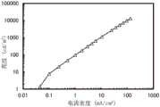
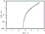
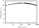
图16示出发光器件1的亮度-电流密度特性;FIG. 16 shows luminance-current density characteristics of the light-emitting
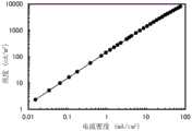
图17示出发光器件1的电流效率-亮度特性;FIG. 17 shows the current efficiency-brightness characteristics of the light-emitting
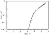
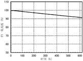
图18示出发光器件1的亮度-电压特性;FIG. 18 shows luminance-voltage characteristics of the light-emitting
图19示出发光器件1的电流-电压特性;FIG. 19 shows the current-voltage characteristics of the light-emitting
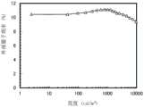
图20示出发光器件1的外部量子效率-亮度特性;FIG. 20 shows the external quantum efficiency-brightness characteristics of the light-emitting
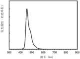
图21示出发光器件1的发射光谱;FIG. 21 shows the emission spectrum of the light-emitting
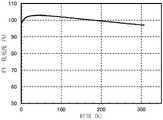
图22示出发光器件1的归一化亮度-时间变化特性;FIG. 22 shows the normalized luminance-time variation characteristics of the light-emitting
图23示出发光器件2的亮度-电流密度特性;FIG. 23 shows luminance-current density characteristics of the light-emitting
图24示出发光器件2的电流效率-亮度特性;FIG. 24 shows the current efficiency-brightness characteristics of the light-emitting
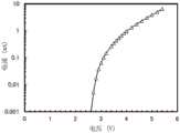
图25示出发光器件2的亮度-电压特性;FIG. 25 shows luminance-voltage characteristics of the light-emitting
图26示出发光器件2的电流-电压特性;FIG. 26 shows the current-voltage characteristics of the light-emitting
图27示出发光器件2的外部量子效率-亮度特性;FIG. 27 shows the external quantum efficiency-brightness characteristics of the light-emitting
图28示出发光器件2的发射光谱;FIG. 28 shows the emission spectrum of the light-emitting
图29示出发光器件2的归一化亮度-时间变化特性;FIG. 29 shows the normalized luminance-time variation characteristics of the light-emitting
图30示出发光器件3的亮度-电流密度特性;FIG. 30 shows luminance-current density characteristics of the light-emitting
图31示出发光器件3的电流效率-亮度特性;FIG. 31 shows the current efficiency-brightness characteristics of the light-emitting
图32示出发光器件3的亮度-电压特性;FIG. 32 shows luminance-voltage characteristics of the light-emitting
图33示出发光器件3的电流-电压特性;FIG. 33 shows the current-voltage characteristics of the light-emitting
图34示出发光器件3的外部量子效率-亮度特性;FIG. 34 shows the external quantum efficiency-brightness characteristics of the light-emitting
图35示出发光器件3的发射光谱;FIG. 35 shows the emission spectrum of the light-emitting
图36示出发光器件3的归一化亮度-时间变化特性;FIG. 36 shows the normalized luminance-time variation characteristics of the light-emitting
图37是示出仅电子元件的结构的图;37 is a diagram showing the structure of only electronic components;
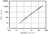
图38示出仅电子元件的电流密度-电压特性;Figure 38 shows the current density-voltage characteristics of only electronic components;
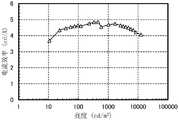
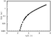
图39示出直流电压为7.0V且ZADN:Liq为1:1时算出的电容C的频率特性;Figure 39 shows the frequency characteristics of the capacitance C calculated when the DC voltage is 7.0V and ZADN:Liq is 1:1;
图40示出直流电压为7.0V且ZADN:Liq为1:1时的-ΔB的频率特性;Fig. 40 shows the frequency characteristic of -ΔB when the DC voltage is 7.0V and ZADN:Liq is 1:1;
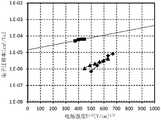
图41示出各有机化合物的电子迁移率的电场强度依赖性;Figure 41 shows the electric field intensity dependence of electron mobility for each organic compound;
图42示出发光器件4的亮度-电流密度特性;FIG. 42 shows luminance-current density characteristics of the light-emitting
图43示出发光器件4的电流效率-亮度特性;FIG. 43 shows the current efficiency-brightness characteristics of the light-emitting
图44示出发光器件4的亮度-电压特性;FIG. 44 shows luminance-voltage characteristics of the light-emitting
图45示出发光器件4的电流-电压特性;FIG. 45 shows the current-voltage characteristics of the light-emitting
图46示出发光器件4的外部量子效率-亮度特性;FIG. 46 shows the external quantum efficiency-brightness characteristics of the light-emitting
图47示出发光器件4的发射光谱;Figure 47 shows the emission spectrum of the light-emitting
图48示出发光器件4的归一化亮度-时间变化特性;FIG. 48 shows the normalized luminance-time variation characteristics of the light-emitting
图49示出发光器件5的亮度-电流密度特性;FIG. 49 shows luminance-current density characteristics of the light-emitting
图50示出发光器件5的电流效率-亮度特性;FIG. 50 shows the current efficiency-brightness characteristics of the light-emitting
图51示出发光器件5的亮度-电压特性;FIG. 51 shows luminance-voltage characteristics of the light-emitting
图52示出发光器件5的电流-电压特性;FIG. 52 shows the current-voltage characteristics of the light-emitting
图53示出发光器件5的外部量子效率-亮度特性;FIG. 53 shows the external quantum efficiency-brightness characteristics of the light-emitting
图54示出发光器件5的发射光谱;FIG. 54 shows the emission spectrum of the light-emitting
图55示出发光器件5的归一化亮度-时间变化特性;FIG. 55 shows the normalized luminance-time variation characteristics of the light-emitting
图56示出发光器件6的亮度-电流密度特性;FIG. 56 shows the luminance-current density characteristics of the light-emitting
图57示出发光器件6的电流效率-亮度特性;FIG. 57 shows the current efficiency-brightness characteristics of the light-emitting
图58示出发光器件6的亮度-电压特性;FIG. 58 shows luminance-voltage characteristics of the light-emitting
图59示出发光器件6的电流-电压特性;FIG. 59 shows the current-voltage characteristics of the light-emitting
图60示出发光器件6的外部量子效率-亮度特性;FIG. 60 shows the external quantum efficiency-brightness characteristics of the light-emitting
图61示出发光器件6的发射光谱;Figure 61 shows the emission spectrum of the light-emitting
图62示出发光器件6的归一化亮度-时间变化特性;FIG. 62 shows the normalized luminance-time variation characteristics of the light-emitting
图63示出发光器件7的亮度-电流密度特性;FIG. 63 shows luminance-current density characteristics of the light-emitting
图64示出发光器件7的电流效率-亮度特性;FIG. 64 shows the current efficiency-brightness characteristics of the light-emitting
图65示出发光器件7的亮度-电压特性;FIG. 65 shows luminance-voltage characteristics of the light-emitting
图66示出发光器件7的电流-电压特性;FIG. 66 shows the current-voltage characteristics of the light-emitting
图67示出发光器件7的外部量子效率-亮度特性;FIG. 67 shows the external quantum efficiency-brightness characteristics of the light-emitting
图68示出发光器件7的发射光谱;FIG. 68 shows the emission spectrum of the light-emitting
图69示出发光器件7的归一化亮度-时间变化特性;FIG. 69 shows the normalized luminance-time variation characteristics of the light-emitting
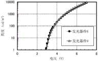
图70示出发光器件8及发光器件9的亮度-电流密度特性;FIG. 70 shows luminance-current density characteristics of light-emitting
图71示出发光器件8及发光器件9的电流效率-亮度特性;FIG. 71 shows the current efficiency-brightness characteristics of the light-emitting
图72示出发光器件8及发光器件9的亮度-电压特性;FIG. 72 shows luminance-voltage characteristics of light-emitting
图73示出发光器件8及发光器件9的电流-电压特性;FIG. 73 shows the current-voltage characteristics of the light-emitting
图74示出发光器件8及发光器件9的外部量子效率-亮度特性;FIG. 74 shows the external quantum efficiency-brightness characteristics of light-emitting
图75示出发光器件8及发光器件9的发射光谱;FIG. 75 shows the emission spectra of light-emitting
图76示出发光器件8及发光器件9的归一化亮度-时间变化特性。FIG. 76 shows the normalized luminance-time variation characteristics of the light-emitting
具体实施方式Detailed ways
以下,参照附图详细地说明本发明的实施方式。但是,本发明不局限于以下说明,而所属技术领域的普通技术人员可以很容易地理解一个事实就是其方式及详细内容在不脱离本发明的宗旨及其范围的情况下可以被变换为各种各样的形式。因此,本发明的一个实施方式不应该被解释为仅局限在以下所示的实施方式所记载的内容中。Hereinafter, embodiments of the present invention will be described in detail with reference to the accompanying drawings. However, the present invention is not limited to the following description, and those skilled in the art can easily understand the fact that the mode and details can be changed into various forms without departing from the spirit and scope of the present invention. various forms. Therefore, one embodiment of the present invention should not be construed as being limited to the contents described in the embodiments shown below.
(实施方式1)(Embodiment 1)
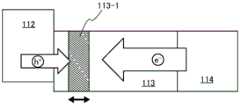
图1A是示出本发明的一个实施方式的发光器件的图。本发明的一个实施方式的发光器件包括阳极101、阴极102、EL层103,该EL层包括空穴注入层111、空穴传输层112、发光层113以及电子传输层114。FIG. 1A is a diagram showing a light emitting device according to an embodiment of the present invention. A light emitting device according to an embodiment of the present invention includes an
虽然在图1A中的EL层103中除了上述以外还示出电子注入层115,但是发光器件的结构不局限于此。只要具有上述结构,就也可以包括具有其他功能的层。Although the
空穴注入层111包括第一有机化合物及第二有机化合物。第一有机化合物是对第二有机化合物呈现电子接受性的物质。第二有机化合物是HOMO能级为-5.7eV以上且-5.4eV以下的具有较深HOMO能级的物质。通过使第二有机化合物具有较深的HOMO能级可以容易地向空穴传输层112注入空穴。The
第一有机化合物可以使用具有吸电子基团(尤其是氟基那样的卤基或氰基)的有机化合物等,可以从这样的物质中适当地选择对上述第二有机化合物呈现电子接受性的物质。作为这种有机化合物,可以举出7,7,8,8-四氰基-2,3,5,6-四氟醌二甲烷(简称:F4-TCNQ)、氯醌、2,3,6,7,10,11-六氰-1,4,5,8,9,12-六氮杂三亚苯(简称:HAT-CN)、1,3,4,5,7,8-六氟四氰(hexafluorotetracyano)-萘醌二甲烷(naphthoquinodimethane)(简称:F6-TCNNQ)、2-(7-二氰基亚甲基-1,3,4,5,6,8,9,10-八氟-7H-芘-2-亚基)丙二腈等。吸电子基团键合于具有多个杂原子的稠合芳香环的化合物诸如HAT-CN等热稳定,所以是优选的。包括吸电子基团(尤其是如氟基等卤基、氰基)的[3]轴烯衍生物的电子接收性非常高所以是优选的,具体而言,可以举出:α,α’,α”-1,2,3-环丙烷三亚基三[4-氰-2,3,5,6-四氟苯乙腈]、α,α’,α”-1,2,3-环丙烷三亚基三[2,6-二氯-3,5-二氟-4-(三氟甲基)苯乙腈]、α,α’,α”-1,2,3-环丙烷三亚基三[2,3,4,5,6-五氟苯乙腈]等。As the first organic compound, an organic compound having an electron-withdrawing group (especially a halogen group such as a fluorine group or a cyano group) can be used, and a substance exhibiting electron accepting property for the second organic compound can be appropriately selected from such substances. . Examples of such organic compounds include 7,7,8,8-tetracyano-2,3,5,6-tetrafluoroquinodimethane (abbreviation: F4 -TCNQ), chloranil, 2,3, 6,7,10,11-hexacyano-1,4,5,8,9,12-hexaazatriphenylene (abbreviation: HAT-CN), 1,3,4,5,7,8-hexafluoro Hexafluorotetracyano-naphthoquinodimethane (abbreviation: F6-TCNNQ), 2-(7-dicyanomethylene-1,3,4,5,6,8,9,10-octa Fluoro-7H-pyrene-2-ylidene) malononitrile, etc. Compounds in which the electron withdrawing group is bonded to a condensed aromatic ring having a plurality of heteroatoms such as HAT-CN are thermally stable and therefore preferred. [3] Axylene derivatives including electron withdrawing groups (especially halogen groups such as fluorine groups, cyano groups) are preferable because of their very high electron accepting properties. Specifically, α, α', α"-1,2,3-cyclopropanetriidene tris[4-cyano-2,3,5,6-tetrafluorobenzeneacetonitrile], α,α',α"-1,2,3-cyclopropanetriidene Tris[2,6-dichloro-3,5-difluoro-4-(trifluoromethyl)benzeneacetonitrile], α,α',α"-1,2,3-cyclopropanetriylidenetri[2 , 3,4,5,6-pentafluorobenzeneacetonitrile] and so on.
第二有机化合物优选为具有空穴传输性的有机化合物,优选具有咔唑骨架、二苯并呋喃骨架、二苯并噻吩骨架及蒽骨架中的任意个。尤其是,可以为具有包括二苯并呋喃环或二苯并噻吩环的取代基的芳香胺、包括萘环的芳香单胺、或者9-芴基通过亚芳基键合于胺的氮的芳香单胺。注意,当这些第二有机化合物是包括N,N-双(4-联苯)氨基的物质时,可以制造寿命良好的发光器件,所以是优选的。作为上述第二有机化合物,具体而言,可以举出N-(4-联苯)-6,N-二苯基苯并[b]萘并[1,2-d]呋喃-8-胺(简称:BnfABP)、N,N-双(4-联苯)-6-苯基苯并[b]萘并[1,2-d]呋喃-8-胺(简称:BBABnf)、4,4’-双(6-苯基苯并[b]萘并[1,2-d]呋喃-8-基)-4”-苯基三苯基胺(简称:BnfBB1BP)、N,N-双(4-联苯)苯并[b]萘并[1,2-d]呋喃-6-胺(简称:BBABnf(6))、N,N-双(4-联苯)苯并[b]萘并[1,2-d]呋喃-8-胺(简称:BBABnf(8))、N,N-双(4-联苯)苯并[b]萘并[2,3-d]呋喃-4-胺(简称:BBABnf(II)(4))、N,N-双[4-(二苯并呋喃-4-基)苯基]-4-氨基-p-三联苯基(简称:DBfBB1TP)、N-[4-(二苯并噻吩-4-基)苯基]-N-苯基-4-联苯胺(简称:ThBA1BP)、4-(2-萘基)-4’,4”-二苯基三苯基胺(简称:BBAβNB)、4-[4-(2-萘基)苯基]-4’,4”-二苯基三苯基胺(简称:BBAβNBi)、4-(2;1’-联萘基-6-基)-4’,4”-二苯基三苯基胺(简称:BBAαNβNB)、4,4’-二苯基-4”-(7;1’-联萘基-2-基)三苯基胺(简称:BBAαNβNB-03)、4,4’-二苯基-4”-(7-苯基)萘基-2-基三苯基胺(简称:BBAPβNB-03)、4-(6;2’-联萘基-2-基)-4’,4”-二苯基三苯基胺(简称:BBA(βN2)B)、4-(2;2’-联萘基-7-基)-4’,4”-二苯基三苯基胺(简称:BBA(βN2)B-03)、4-(1;2’-联萘基-4-基)-4’,4”-二苯基三苯基胺(简称:BBAβNαNB)、4-(1;2’-联萘基-5-基)-4’,4”-二苯基三苯基胺(简称:BBAβNαNB-02)、4-(4-联苯基)-4’-(2-萘基)-4”-苯基三苯基胺(简称:TPBiAβNB)、4-(3-联苯基)-4’-[4-(2-萘基)苯基]-4”-苯基三苯基胺(简称:mTPBiAβNBi)、4-(4-联苯基)-4’-[4-(2-萘基)苯基]-4”-苯基三苯基胺(简称:TPBiAβNBi)、4-(1-萘基)-4’-苯基三苯基胺(简称:αNBA1BP)、4,4’-双(1-萘基)三苯基胺(简称:αNBB1BP)、4,4’-二苯基-4”-[4’-(咔唑-9-基)联苯-4-基]三苯基胺(简称:YGTBi1BP)、4’-[4-(3-苯基-9H-咔唑-9-基)苯基]三(1,1’-联苯-4-基)胺(简称:YGTBi1BP-02)、4-[4’-(咔唑-9-基)联苯-4-基]-4’-(2-萘基)-4”-苯基三苯基胺(简称:YGTBiβNB)、N-[4-(9-苯基-9H-咔唑-3-基)苯基]-N-[4-(1-萘基)苯基]-9,9'-螺双[9H-芴]-2-胺(简称:PCBNBSF)、N,N-双([1,1'-联苯基]-4-基)-9,9’-螺双[9H-芴]-2-胺(简称:BBASF)、N,N-双([1,1’-联苯基]-4-基)-9,9’-螺双[9H-芴]-4-胺(简称:BBASF(4))、N-(1,1’-联苯-2-基)-N-(9,9-二甲基-9H-芴-2-基)-9,9’-螺-双(9H-芴)-4-胺(简称:oFBiSF)、N-(4-联苯基)-N-(9,9-二甲基-9H-芴-2-基)二苯并呋喃-4-胺(简称:FrBiF)、N-[4-(1-萘基)苯基]-N-[3-(6-苯基二苯并呋喃-4-基)苯基]-1-萘基胺(简称:mPDBfBNBN)、4-苯基-4’-(9-苯基芴-9-基)三苯基胺(简称:BPAFLP)、4-苯基-3’-(9-苯基芴-9-基)三苯基胺(简称:mBPAFLP)、4-苯基-4’-[4-(9-苯基芴-9-基)苯基]三苯基胺(简称:BPAFLBi)、4-苯基-4’-(9-苯基-9H-咔唑-3-基)三苯基胺(简称:PCBA1BP)、4,4’-二苯基-4”-(9-苯基-9H-咔唑-3-基)三苯基胺(简称:PCBBi1BP)、4-(1-萘基)-4’-(9-苯基-9H-咔唑-3-基)三苯基胺(简称:PCBANB)、4,4’-二(1-萘基)-4”-(9-苯基-9H-咔唑-3-基)三苯基胺(简称:PCBNBB)、N-苯基-N-[4-(9-苯基-9H-咔唑-3-基)苯基]-9,9’-螺双[9H-芴]-2-胺(简称:PCBASF)、N-(1,1’-联苯-4-基)-9,9-二甲基-N-[4-(9-苯基-9H-咔唑-3-基)苯基]-9H-芴-2-胺(简称:PCBBiF)等。The second organic compound is preferably an organic compound having hole transport properties, and preferably has any one of a carbazole skeleton, a dibenzofuran skeleton, a dibenzothiophene skeleton, and an anthracene skeleton. In particular, it may be an aromatic amine having a substituent including a dibenzofuran ring or a dibenzothiophene ring, an aromatic monoamine including a naphthalene ring, or an aromatic in which a 9-fluorenyl group is bonded to the nitrogen of the amine through an arylene group Monoamine. Note that when these second organic compounds are substances including N,N-bis(4-biphenyl)amino groups, it is possible to manufacture a light-emitting device with a good lifetime, so it is preferable. Specific examples of the second organic compound include N-(4-biphenyl)-6,N-diphenylbenzo[b]naphtho[1,2-d]furan-8-amine ( Abbreviation: BnfABP), N,N-bis(4-biphenyl)-6-phenylbenzo[b]naphtho[1,2-d]furan-8-amine (abbreviation: BBABnf), 4,4' -Bis(6-phenylbenzo[b]naphtho[1,2-d]furan-8-yl)-4"-phenyltriphenylamine (abbreviation: BnfBB1BP), N,N-bis(4 - Biphenyl)benzo[b]naphtho[1,2-d]furan-6-amine (abbreviation: BBABnf(6)), N,N-bis(4-biphenyl)benzo[b]naphtho [1,2-d]furan-8-amine (abbreviation: BBABnf(8)), N,N-bis(4-biphenyl)benzo[b]naphtho[2,3-d]furan-4- Amine (abbreviation: BBABnf(II)(4)), N,N-bis[4-(dibenzofuran-4-yl)phenyl]-4-amino-p-terphenyl (abbreviation: DBfBB1TP), N-[4-(Dibenzothiophen-4-yl)phenyl]-N-phenyl-4-benzidine (abbreviation: ThBA1BP), 4-(2-naphthyl)-4', 4"-di Phenyltriphenylamine (abbreviation: BBAβNB), 4-[4-(2-naphthyl)phenyl]-4', 4"-diphenyltriphenylamine (abbreviation: BBAβNBi), 4-(2 ;1'-Binaphthyl-6-yl)-4',4"-diphenyltriphenylamine (abbreviation: BBAαNβNB), 4,4'-diphenyl-4"-(7;1'- Binaphthyl-2-yl)triphenylamine (abbreviation: BBAαNβNB-03), 4,4'-diphenyl-4"-(7-phenyl)naphthyl-2-yltriphenylamine (abbreviation: BBAαNβNB-03) : BBAPβNB-03), 4-(6; 2'-binaphthyl-2-yl)-4', 4"-diphenyltriphenylamine (abbreviation: BBA(βN2)B), 4-(2 ; 2'-binaphthyl-7-yl)-4', 4"-diphenyltriphenylamine (abbreviation: BBA(βN2)B-03), 4-(1; 2'-binaphthyl- 4-yl)-4',4"-diphenyltriphenylamine (abbreviation: BBAβNαNB), 4-(1;2'-binaphthyl-5-yl)-4',4"-diphenyl Triphenylamine (abbreviation: BBAβNαNB-02), 4-(4-biphenyl)-4'-(2-naphthyl)-4"-phenyltriphenylamine (abbreviation: TPBiAβNB), 4-( 3-biphenyl)-4'-[4-(2-naphthyl)phenyl]-4"-phenyltriphenylamine (abbreviation: mTPBiAβNBi), 4-(4-biphenyl)-4' -[4-(2-Naphthyl)phenyl]-4"-phenyltriphenylamine (abbreviation: TPBiAβNBi), 4-(1-naphthyl)-4'-phenyltriphenylamine (abbreviation: αNBA1BP), 4,4'-bis(1-naphthyl)triphenylamine (abbreviation: αNBB1 BP), 4,4'-diphenyl-4"-[4'-(carbazol-9-yl)biphenyl-4-yl]triphenylamine (abbreviation: YGTBi1BP), 4'-[4- (3-phenyl-9H-carbazol-9-yl)phenyl]tris(1,1'-biphenyl-4-yl)amine (abbreviation: YGTBi1BP-02), 4-[4'-(carbazole) -9-yl)biphenyl-4-yl]-4'-(2-naphthyl)-4"-phenyltriphenylamine (abbreviation: YGTBiβNB), N-[4-(9-phenyl-9H -Carbazol-3-yl)phenyl]-N-[4-(1-naphthyl)phenyl]-9,9'-spirobis[9H-fluorene]-2-amine (abbreviation: PCBNBSF), N , N-bis([1,1'-biphenyl]-4-yl)-9,9'-spirobis[9H-fluorene]-2-amine (abbreviation: BBASF), N,N-bis([ 1,1'-Biphenyl]-4-yl)-9,9'-spirobis[9H-fluorene]-4-amine (abbreviation: BBASF(4)), N-(1,1'-biphenyl -2-yl)-N-(9,9-dimethyl-9H-fluoren-2-yl)-9,9'-spiro-bis(9H-fluorene)-4-amine (abbreviation: oFBiSF), N -(4-biphenyl)-N-(9,9-dimethyl-9H-fluoren-2-yl)dibenzofuran-4-amine (abbreviation: FrBiF), N-[4-(1- Naphthyl)phenyl]-N-[3-(6-phenyldibenzofuran-4-yl)phenyl]-1-naphthylamine (abbreviation: mPDBfBNBN), 4-phenyl-4'-( 9-Phenylfluoren-9-yl)triphenylamine (abbreviation: BPAFLP), 4-phenyl-3'-(9-phenylfluoren-9-yl)triphenylamine (abbreviation: mBPAFLP), 4 -Phenyl-4'-[4-(9-phenylfluoren-9-yl)phenyl]triphenylamine (abbreviation: BPAFLBi), 4-phenyl-4'-(9-phenyl-9H- Carbazol-3-yl)triphenylamine (abbreviation: PCBA1BP), 4,4'-diphenyl-4"-(9-phenyl-9H-carbazol-3-yl)triphenylamine (abbreviation: PCBA1BP) : PCBBi1BP), 4-(1-naphthyl)-4'-(9-phenyl-9H-carbazol-3-yl)triphenylamine (abbreviation: PCBANB), 4,4'-bis(1- Naphthyl)-4"-(9-phenyl-9H-carbazol-3-yl)triphenylamine (abbreviation: PCBNBB), N-phenyl-N-[4-(9-phenyl-9H- Carbazol-3-yl)phenyl]-9,9'-spirobis[9H-fluorene]-2-amine (abbreviation: PCBASF), N-(1,1'-biphenyl-4-yl)-9 , 9-dimethyl-N-[4-(9-phenyl-9H-carbazol-3-yl)phenyl]-9H-fluorene-2-amine (abbreviation: PCBBiF) and the like.
空穴传输层112包括第一空穴传输层112-1和第二空穴传输层112-2。第一空穴传输层112-1位于比第二空穴传输层112-2更靠近阳极101一侧。注意,有时第二空穴传输层112-2还同时具有电子阻挡层的功能。The
第一空穴传输层112-1包括第三有机化合物,第二空穴传输层112-2包括第四有机化合物。The first hole transport layer 112-1 includes a third organic compound, and the second hole transport layer 112-2 includes a fourth organic compound.
第三有机化合物及第四有机化合物优选为具有空穴传输性的有机化合物。第三有机化合物及第四有机化合物可以同样地使用能够用作上述第二有机化合物的有机化合物。The third organic compound and the fourth organic compound are preferably organic compounds having hole transport properties. The third organic compound and the fourth organic compound can be similarly used as the organic compound which can be used as the above-mentioned second organic compound.
作为第二有机化合物的HOMO能级和第三有机化合物的HOMO能级,优选以第三有机化合物的HOMO能级更深且其差为0.2eV以下的方式选择各个材料。更优选的是,第二有机化合物和第三有机化合物为相同物质。As the HOMO level of the second organic compound and the HOMO level of the third organic compound, each material is preferably selected so that the HOMO level of the third organic compound is deeper and the difference is 0.2 eV or less. More preferably, the second organic compound and the third organic compound are the same substance.
另外,作为第三有机化合物的HOMO能级和第四有机化合物的HOMO能级,优选第四有机化合物的HOMO能级更深。优选以其差为0.2eV以下的方式选择各自的材料。通过使第二有机化合物至第四有机化合物的HOMO能级具有上述关系,可以使空穴顺利地注入到各层中,由此可以防止驱动电压上升及发光层中空穴过少的状态。In addition, as the HOMO energy level of the third organic compound and the HOMO energy level of the fourth organic compound, it is preferable that the HOMO energy level of the fourth organic compound is deeper. The respective materials are preferably selected so that the difference is 0.2 eV or less. By making the HOMO levels of the second to fourth organic compounds have the above relationship, holes can be smoothly injected into each layer, thereby preventing an increase in the driving voltage and a state where there are too few holes in the light-emitting layer.
优选的是,第二有机化合物至第四有机化合物分别具有空穴传输性骨架。作为该空穴传输性骨架,优选使用不会使上述有机化合物的HOMO能级过浅的咔唑骨架、二苯并呋喃骨架、二苯并噻吩骨架及蒽骨架。当相邻层的材料(例如第二有机化合物和第三有机化合物或第三有机化合物和第四有机化合物)中共用上述空穴传输性骨架时,可以顺利地进行空穴注入,所以是优选的。作为上述空穴传输性骨架尤其优选使用二苯并呋喃骨架。Preferably, the second to fourth organic compounds each have a hole-transporting skeleton. As the hole-transporting skeleton, it is preferable to use a carbazole skeleton, a dibenzofuran skeleton, a dibenzothiophene skeleton, and an anthracene skeleton which do not make the HOMO level of the organic compound too shallow. When the above-mentioned hole-transporting skeleton is shared among the materials of adjacent layers (for example, the second organic compound and the third organic compound or the third organic compound and the fourth organic compound), hole injection can be smoothly performed, so it is preferable . It is particularly preferable to use a dibenzofuran skeleton as the hole-transporting skeleton.
另外,通过使相邻层包含的材料(例如第二有机化合物和第三有机化合物或第三有机化合物和第四有机化合物)为相同材料可以顺利地进行空穴的注入,因此是优选的结构。尤其优选第二有机化合物和第三有机化合物为相同材料。In addition, since the injection of holes can be smoothly performed by making the materials (for example, the second organic compound and the third organic compound or the third organic compound and the fourth organic compound) contained in the adjacent layers the same material, it is a preferable structure. It is especially preferable that the second organic compound and the third organic compound are the same material.
发光层113包括第五有机化合物和第六有机化合物。第五有机化合物为发光中心物质,第六有机化合物是用来分散第五有机化合物的主体材料。The
发光中心材料可以是荧光发光物质、磷光发光物质、呈现热活化延迟荧光(TADF)的物质或其他发光材料。另外,可以为单层,也可以由包含不同发光材料的多个层构成。注意,在本发明的一个实施方式中,优选将发光层113用作呈现荧光发光的层,尤其是,呈现蓝色荧光发光的层。The light-emitting center material may be a fluorescent light-emitting substance, a phosphorescent light-emitting substance, a substance exhibiting thermally activated delayed fluorescence (TADF), or other light-emitting materials. In addition, it may be a single layer, or may be composed of a plurality of layers including different light-emitting materials. Note that, in one embodiment of the present invention, the light-emitting
在发光层113中,作为可以用作荧光发光物质的材料,例如,可以举出5,6-双[4-(10-苯基-9-蒽基)苯基]-2,2'-联吡啶(简称:PAP2BPy)、5,6-双[4'-(10-苯基-9-蒽基)联苯基-4-基]-2,2'-联吡啶(简称:PAPP2BPy)、N,N’-二苯基-N,N’-双[4-(9-苯基-9H-芴-9-基)苯基]芘-1,6-二胺(简称:1,6FLPAPrn)、N,N’-双(3-甲基苯基)-N,N’-双[3-(9-苯基-9H-芴-9-基)苯基]芘-1,6-二胺(简称:1,6mMemFLPAPrn)、N,N'-双[4-(9H-咔唑-9-基)苯基]-N,N'-二苯基二苯乙烯-4,4'-二胺(简称:YGA2S)、4-(9H-咔唑-9-基)-4'-(10-苯基-9-蒽基)三苯胺(简称:YGAPA)、4-(9H-咔唑-9-基)-4'-(9,10-二苯基-2-蒽基)三苯胺(简称:2YGAPPA)、N,9-二苯基-N-[4-(10-苯基-9-蒽基)苯基]-9H-咔唑-3-胺(简称:PCAPA)、二萘嵌苯、2,5,8,11-四(叔丁基)二萘嵌苯(简称:TBP)、4-(10-苯基-9-蒽基)-4'-(9-苯基-9H-咔唑-3-基)三苯胺(简称:PCBAPA)、N,N”-(2-叔丁基蒽-9,10-二基二-4,1-亚苯基)双[N,N',N'-三苯基-1,4-苯二胺](简称:DPABPA)、N,9-二苯基-N-[4-(9,10-二苯基-2-蒽基)苯基]-9H-咔唑-3-胺(简称:2PCAPPA)、N-[4-(9,10-二苯基-2-蒽基)苯基]-N,N',N'-三苯基-1,4-苯二胺(简称:2DPAPPA)、N,N,N',N',N”,N”,N”',N”'-八苯基二苯并[g,p]
在发光层113中,当作为发光中心材料使用磷光发光物质时,例如可以使用如下材料,三{2-[5-(2-甲基苯基)-4-(2,6-二甲基苯基)-4H-1,2,4-三唑-3-基-κN2]苯基-κC}铱(III)(简称:[Ir(mpptz-dmp)3])、三(5-甲基-3,4-二苯基-4H-1,2,4-三唑)铱(III)(简称:[Ir(Mptz)3])、三[4-(3-联苯)-5-异丙基-3-苯基-4H-1,2,4-三唑]铱(III)(简称:[Ir(iPrptz-3b)3])等具有4H-三唑骨架的有机金属铱配合物;三[3-甲基-1-(2-甲基苯基)-5-苯基-1H-1,2,4-三唑]铱(III)(简称:[Ir(Mptz1-mp)3])、三(1-甲基-5-苯基-3-丙基-1H-1,2,4-三唑)铱(III)(简称:[Ir(Prptz1-Me)3])等具有1H-三唑骨架的有机金属铱配合物;fac-三[1-(2,6-二异丙基苯基)-2-苯基-1H-咪唑]铱(III)(简称:[Ir(iPrpmi)3])、三[3-(2,6-二甲基苯基)-7-甲基咪唑并[1,2-f]菲啶根(phenanthridinato)]铱(III)(简称:[Ir(dmpimpt-Me)3])等具有咪唑骨架的有机金属铱配合物;以及双[2-(4',6'-二氟苯基)吡啶根-N,C2']铱(III)四(1-吡唑基)硼酸盐(简称:FIr6)、双[2-(4',6'-二氟苯基)吡啶根-N,C2']铱(III)吡啶甲酸酯(简称:FIrpic)、双{2-[3',5'-双(三氟甲基)苯基]吡啶根-N,C2'}铱(III)吡啶甲酸酯(简称:[Ir(CF3ppy)2(pic)])、双[2-(4',6'-二氟苯基)吡啶根-N,C2']铱(III)乙酰丙酮(简称:FIr(acac))等以具有拉电子基的苯基吡啶衍生物为配体的有机金属铱配合物。上述物质是发射蓝色磷光的化合物,并且是在440nm至520nm具有发光峰的化合物。In the light-emitting layer 113, when a phosphorescent light-emitting substance is used as the light-emitting center material, for example, a material such as tris{2-[5-(2-methylphenyl)-4-(2,6-dimethylbenzene) can be used base)-4H-1,2,4-triazol-3-yl-κN2]phenyl-κC}iridium(III) (abbreviation: [Ir(mpptz-dmp)3 ]), tris(5-methyl- 3,4-diphenyl-4H-1,2,4-triazole) iridium (III) (abbreviation: [Ir(Mptz)3 ]), tris[4-(3-biphenyl)-5-isopropyl Organometallic iridium complexes with 4H-triazole skeleton, such as base-3-phenyl-4H-1,2,4-triazole]iridium (III) (abbreviation: [Ir(iPrptz-3b)3 ]); three [3-Methyl-1-(2-methylphenyl)-5-phenyl-1H-1,2,4-triazole]iridium(III) (abbreviation: [Ir(Mptz1-mp)3 ]) , tris (1-methyl-5-phenyl-3-propyl-1H-1,2,4-triazole) iridium (III) (abbreviation: [Ir(Prptz1-Me)3 ]) etc. have 1H- Organometallic iridium complexes with triazole skeleton; fac-tris[1-(2,6-diisopropylphenyl)-2-phenyl-1H-imidazole]iridium(III) (abbreviation: [Ir(iPrpmi)]3 ]), tris[3-(2,6-dimethylphenyl)-7-methylimidazo[1,2-f]phenanthridinato]iridium(III) (abbreviation: [Ir( dmpimpt-Me)3 ]) and other organometallic iridium complexes with imidazole skeleton; and bis[2-(4',6'-difluorophenyl)pyridine-N,C2 ']iridium(III)tetra 1-Pyrazolyl) borate (abbreviation: FIr6), bis[2-(4',6'-difluorophenyl)pyridino-N,C2 ']iridium(III) picolinate (abbreviation: FIr6) : FIrpic), bis{2-[3',5'-bis(trifluoromethyl)phenyl]pyridine-N,C2 '}iridium(III) picolinate (abbreviation: [Ir(CF3) ppy)2 (pic)]), bis[2-(4',6'-difluorophenyl)pyridine-N,C2 ']iridium(III) acetylacetone (abbreviation: FIr(acac)), etc. Phenylpyridine derivatives with electron withdrawing groups are organometallic iridium complexes of ligands. The above-mentioned substances are compounds that emit blue phosphorescence, and are compounds that have an emission peak at 440 nm to 520 nm.
另外,可以举出:三(4-甲基-6-苯基嘧啶根)铱(III)(简称:[Ir(mppm)3])、三(4-叔丁基-6-苯基嘧啶根)铱(III)(简称:[Ir(tBuppm)3])、(乙酰丙酮根)双(6-甲基-4-苯基嘧啶根)铱(III)(简称:[Ir(mppm)2(acac)])、(乙酰丙酮根)双(6-叔丁基-4-苯基嘧啶根)铱(III)(简称:[Ir(tBuppm)2(acac)])、(乙酰丙酮根)双[6-(2-降冰片基)-4-苯基嘧啶根]铱(III)(简称:[Ir(nbppm)2(acac)])、(乙酰丙酮根)双[5-甲基-6-(2-甲基苯基)-4-苯基嘧啶根]铱(III)(简称:Ir(mpmppm)2(acac))、(乙酰丙酮根)双(4,6-二苯基嘧啶根)铱(III)(简称:[Ir(dppm)2(acac)])等具有嘧啶骨架的有机金属铱配合物;(乙酰丙酮根)双(3,5-二甲基-2-苯基吡嗪根)铱(III)(简称:[Ir(mppr-Me)2(acac)])、(乙酰丙酮根)双(5-异丙基-3-甲基-2-苯基吡嗪根)铱(III)(简称:[Ir(mppr-iPr)2(acac)])等具有吡嗪骨架的有机金属铱配合物;三(2-苯基吡啶根-N,C2')铱(III)(简称:[Ir(ppy)3])、双(2-苯基吡啶根-N,C2')铱(III)乙酰丙酮(简称:[Ir(ppy)2(acac)])、双(苯并[h]喹啉)铱(III)乙酰丙酮(简称:[Ir(bzq)2(acac)])、三(苯并[h]喹啉)铱(III)(简称:[Ir(bzq)3])、三(2-苯基喹啉-N,C2']铱(III)(简称:[Ir(pq)3])、双(2-苯基喹啉-N,C2')铱(III)乙酰丙酮(简称:[Ir(pq)2(acac)])等具有吡啶骨架的有机金属铱配合物;以及三(乙酰丙酮根)(单菲咯啉)铽(III)(简称:[Tb(acac)3(Phen)])等稀土金属配合物。上述物质主要是发射绿色磷光的化合物,并且在500nm至600nm具有发光峰。注意,由于具有嘧啶骨架的有机金属铱配合物具有特别优异的可靠性及发光效率,所以是特别优选的。In addition, tris(4-methyl-6-phenylpyrimidine) iridium (III) (abbreviation: [Ir(mppm)3 ]), tris(4-tert-butyl-6-phenylpyrimidine), ) iridium (III) (abbreviation: [Ir(tBuppm)3 ]), (acetylacetonate) bis(6-methyl-4-phenylpyrimidinyl) iridium (III) (abbreviation: [Ir(mppm)2 ( acac)]), (acetylacetonate) bis (6-tert-butyl-4-phenylpyrimidinyl) iridium (III) (abbreviation: [Ir(tBuppm)2 (acac)]), (acetylacetonate) bis [6-(2-norbornyl)-4-phenylpyrimidinyl]iridium(III) (abbreviation: [Ir(nbppm)2 (acac)]), (acetylacetonate)bis[5-methyl-6 -(2-Methylphenyl)-4-phenylpyrimidine]iridium(III) (abbreviation: Ir(mpmppm)2 (acac)), (acetylacetonate)bis(4,6-diphenylpyrimidine) ) Iridium (III) (abbreviation: [Ir(dppm)2 (acac)]) and other organometallic iridium complexes with a pyrimidine skeleton; (acetylacetonate) bis(3,5-dimethyl-2-phenylpyridine) oxazine) iridium (III) (abbreviation: [Ir(mppr-Me)2 (acac)]), (acetylacetonate) bis(5-isopropyl-3-methyl-2-phenylpyrazine) Iridium (III) (abbreviation: [Ir(mppr-iPr)2 (acac)]) and other organometallic iridium complexes with pyrazine skeleton; tris(2-phenylpyridine-N,C2 ') iridium (III ) (abbreviation: [Ir(ppy)3 ]), bis(2-phenylpyridino-N,C2 ') iridium (III) acetylacetone (abbreviation: [Ir(ppy)2 (acac)]), bis (Benzo[h]quinoline)iridium(III) acetylacetone (abbreviation: [Ir(bzq)2 (acac)]), tris(benzo[h]quinoline)iridium(III) (abbreviation: [Ir( bzq)3 ]), tris(2-phenylquinoline-N,C2 ']iridium(III) (abbreviation: [Ir(pq)3 ]), bis(2-phenylquinoline-N,C2 ') Iridium (III) acetylacetone (abbreviation: [Ir(pq)2 (acac)]) and other organometallic iridium complexes with a pyridine skeleton; and tris (acetylacetonate) (monophenanthroline) terbium (III) (abbreviation: [Tb(acac)3 (Phen)]) and other rare earth metal complexes. The above substances are mainly compounds that emit green phosphorescence, and have a luminescence peak at 500 nm to 600 nm. Note that since the organometallic iridium complex having a pyrimidine skeleton It has particularly excellent reliability and luminous efficiency, so it is particularly preferred.
另外,可以举出:(二异丁酰基甲烷根)双[4,6-双(3-甲基苯基)嘧啶基]铱(III)(简称:[Ir(5mdppm)2(dibm)])、双[4,6-双(3-甲基苯基)嘧啶根)(二新戊酰基甲烷根)铱(III)(简称:[Ir(5mdppm)2(dpm)])、双[4,6-二(萘-1-基)嘧啶根](二新戊酰基甲烷根)铱(III)(简称:[Ir(d1npm)2(dpm)])等具有嘧啶骨架的有机金属铱配合物;(乙酰丙酮根)双(2,3,5-三苯基吡嗪根)铱(III)(简称:[Ir(tppr)2(acac)])、双(2,3,5-三苯基吡嗪根)(二新戊酰基甲烷根)铱(III)(简称:[Ir(tppr)2(dpm)])、(乙酰丙酮根)双[2,3-双(4-氟苯基)喹喔啉合]铱(III)(简称:[Ir(Fdpq)2(acac)])等具有吡嗪骨架的有机金属铱配合物;三(1-苯基异喹啉-N,C2’)铱(III)(简称:[Ir(piq)3])、双(1-苯基异喹啉-N,C2’)铱(III)乙酰丙酮(简称:[Ir(piq)2(acac)])等具有吡啶骨架的有机金属铱配合物;2,3,7,8,12,13,17,18-八乙基-21H,23H-卟啉铂(II)(简称:PtOEP)等的铂配合物;以及三(1,3-二苯基-1,3-丙二酮(propanedionato))(单菲咯啉)铕(III)(简称:[Eu(DBM)3(Phen)])、三[1-(2-噻吩甲酰基)-3,3,3-三氟丙酮](单菲咯啉)铕(III)(简称:[Eu(TTA)3(Phen)])等稀土金属配合物。上述物质是发射红色磷光的化合物,并且在600nm至700nm具有发光峰。另外,具有吡嗪骨架的有机金属铱配合物可以获得色度良好的红色发光。In addition, (diisobutyrylmethanoate)bis[4,6-bis(3-methylphenyl)pyrimidinyl]iridium (III) (abbreviation: [Ir(5mdppm)2 (dibm)]) , bis[4,6-bis(3-methylphenyl)pyrimidine radical) (dipivaloylmethane radical) iridium (III) (abbreviation: [Ir(5mdppm)2 (dpm)]), bis[4, Organometallic iridium complexes with pyrimidine skeletons such as 6-bis(naphthalen-1-yl)pyrimidine radical](dipivaloylmethane radical) iridium (III) (abbreviation: [Ir(d1npm)2 (dpm)]); (Acetylacetonate) bis(2,3,5-triphenylpyrazine) iridium(III) (abbreviation: [Ir(tppr)2 (acac)]), bis(2,3,5-triphenyl) Pyrazine) (Dipivaloylmethane) Iridium (III) (abbreviation: [Ir(tppr)2 (dpm)]), (acetylacetonate) bis[2,3-bis(4-fluorophenyl) Quinoxaline] iridium (III) (abbreviation: [Ir(Fdpq)2 (acac)]) and other organometallic iridium complexes with pyrazine skeleton; tris(1-phenylisoquinoline-N,C2' ) iridium (III) (abbreviation: [Ir(piq)3 ]), bis(1-phenylisoquinoline-N,C2' ) iridium (III) acetylacetone (abbreviation: [Ir(piq)2 (acac )]) and other organometallic iridium complexes with pyridine skeleton; 2,3,7,8,12,13,17,18-octaethyl-21H,23H-porphyrin platinum (II) (abbreviation: PtOEP), etc. and tris(1,3-diphenyl-1,3-propanedione (propanedionato))(monophenanthroline) europium(III) (abbreviation: [Eu(DBM)3 (Phen)] ), tris[1-(2-thiopheneformyl)-3,3,3-trifluoroacetone] (monophenanthroline) europium (III) (abbreviation: [Eu(TTA)3 (Phen)]) and other rare earths metal complexes. The above substances are compounds that emit red phosphorescence, and have a light emission peak at 600 nm to 700 nm. In addition, the organometallic iridium complex having a pyrazine skeleton can obtain red light emission with good chromaticity.
另外,除了上述磷光化合物以外,还可以选择已知的磷光发光材料而使用。In addition to the above-mentioned phosphorescent compounds, known phosphorescent light-emitting materials can be selected and used.
作为TADF材料可以使用富勒烯及其衍生物、吖啶及其衍生物以及伊红衍生物等。另外,还可以举出包含镁(Mg)、锌(Zn)、镉(Cd)、锡(Sn)、铂(Pt)、铟(In)或钯(Pd)等含金属卟啉。作为该含金属卟啉,例如,也可以举出由下述结构式表示的原卟啉-氟化锡配合物(SnF2(Proto IX))、中卟啉-氟化锡配合物(SnF2(Meso IX))、血卟啉-氟化锡配合物(SnF2(Hemato IX))、粪卟啉四甲酯-氟化锡配合物(SnF2(Copro III-4Me)、八乙基卟啉-氟化锡配合物(SnF2(OEP))、初卟啉-氟化锡配合物(SnF2(Etio I))以及八乙基卟啉-氯化铂配合物(PtCl2OEP)等。As the TADF material, fullerene and its derivatives, acridine and its derivatives, and eosin derivatives can be used. In addition, metal-containing porphyrins such as magnesium (Mg), zinc (Zn), cadmium (Cd), tin (Sn), platinum (Pt), indium (In), or palladium (Pd) can also be mentioned. As the metal-containing porphyrin, for example, a protoporphyrin-tin fluoride complex (SnF2 (Proto IX)), a mesoporphyrin-tin fluoride complex (SnF 2 (SnF2 ( Meso IX)), hematoporphyrin-tin fluoride complex (SnF2 (Hemato IX)), coproporphyrin tetramethyl-tin fluoride complex (SnF2 (Copro III-4Me), octaethylporphyrin - Tin fluoride complex (SnF2 (OEP)), protoporphyrin-tin fluoride complex (SnF2 (Etio I)) and octaethylporphyrin-platinum chloride complex (PtCl2 OEP) and the like.
[化学式1][Chemical formula 1]

另外,还可以使用由下述结构式表示的2-(联苯-4-基)-4,6-双(12-苯基吲哚[2,3-a]咔唑-11-基)-1,3,5-三嗪(简称:PIC-TRZ)、9-(4,6-二苯基-1,3,5-三嗪-2-基)-9’-苯基-9H,9’H-3,3’-联咔唑(简称:PCCzTzn)、2-{4-[3-(N-苯基-9H-咔唑-3-基)-9H-咔唑-9-基]苯基}-4,6-二苯基-1,3,5-三嗪(简称:PCCzPTzn)、2-[4-(10H-吩恶嗪-10-基)苯基]-4,6-二苯基-1,3,5-三嗪(简称:PXZ-TRZ)、3-[4-(5-苯基-5,10-二氢吩嗪-10-基)苯基]-4,5-二苯基-1,2,4-三唑(简称:PPZ-3TPT)、3-(9,9-二甲基-9H-吖啶-10-基)-9H-氧杂蒽-9-酮(简称:ACRXTN)、双[4-(9,9-二甲基-9,10-二氢吖啶)苯基]硫砜(简称:DMAC-DPS)、10-苯基-10H,10’H-螺[吖啶-9,9’-蒽]-10’-酮(简称:ACRSA)等具有富π电子型杂芳环和缺π电子型杂芳环的一方或双方的杂环化合物。该杂环化合物具有富π电子型杂芳环和缺π电子型杂芳环,电子传输性和空穴传输性都高,所以是优选的。在具有缺π电子杂芳环的骨架中,吡啶骨架、二嗪骨架(嘧啶骨架、吡嗪骨架、哒嗪骨架)及三嗪骨架稳定且可靠性良好,所以是优选的。尤其是,苯并呋喃并嘧啶骨架、苯并噻吩并嘧啶骨架、苯并呋喃并吡嗪骨架、苯并噻吩并吡嗪骨架的电子接受性高且可靠性良好,所以是优选的。在具有富π电子杂芳环的骨架中,吖啶骨架、吩恶嗪骨架、吩噻嗪骨架、呋喃骨架、噻吩骨架及吡咯骨架稳定且可靠性良好,所以优选具有上述骨架中的至少一个。作为呋喃骨架优选使用二苯并呋喃骨架。作为噻吩骨架优选使用二苯并噻吩骨架。作为吡咯骨架,特别优选使用吲哚骨架、咔唑骨架、吲哚咔唑骨架、联咔唑骨架、3-(9-苯基-9H-咔唑-3-基)-9H-咔唑骨架。注意,在富π电子型芳杂环和缺π电子型芳杂环直接键合的物质中,富π电子芳杂环的电子供给性和缺π电子型芳杂环的电子接受性都高而S1能级与T1能级之间的能量差变小,可以高效地获得热活化延迟荧光,所以是特别优选的。注意,也可以使用键合有氰基等吸电子基团的芳环代替缺π电子型芳杂环。作为富π电子骨架,可以使用芳香胺骨架、吩嗪骨架等。作为缺π电子骨架,可以使用氧杂蒽骨架、二氧化噻吨(thioxanthene dioxide)骨架、噁二唑骨架、三唑骨架、咪唑骨架、蒽醌骨架、苯基硼烷或boranthrene等含硼骨架、苯甲腈或氰苯等具有腈基或氰基的芳香环或杂芳环、二苯甲酮等羰骨架、氧化膦骨架、砜骨架等。如此,可以使用缺π电子骨架及富π电子骨架代替缺π电子杂芳环以及富π电子杂芳环中的至少一个。In addition, 2-(biphenyl-4-yl)-4,6-bis(12-phenylindole[2,3-a]carbazol-11-yl)-1 represented by the following structural formula can also be used ,3,5-triazine (abbreviation: PIC-TRZ), 9-(4,6-diphenyl-1,3,5-triazin-2-yl)-9'-phenyl-9H,9'H-3,3'-bicarbazole (abbreviation: PCCzTzn), 2-{4-[3-(N-phenyl-9H-carbazol-3-yl)-9H-carbazol-9-yl]benzene base}-4,6-diphenyl-1,3,5-triazine (abbreviation: PCCzPTzn), 2-[4-(10H-phenoxazin-10-yl)phenyl]-4,6-di Phenyl-1,3,5-triazine (abbreviation: PXZ-TRZ), 3-[4-(5-phenyl-5,10-dihydrophenazine-10-yl)phenyl]-4,5 -Diphenyl-1,2,4-triazole (abbreviation: PPZ-3TPT), 3-(9,9-dimethyl-9H-acridin-10-yl)-9H-oxanthene-9- Ketone (abbreviation: ACRXTN), bis[4-(9,9-dimethyl-9,10-dihydroacridine)phenyl]thiosulfone (abbreviation: DMAC-DPS), 10-phenyl-10H, 10 'H-spiro[acridine-9,9'-anthracene]-10'-one (abbreviation: ACRSA) and other heterocyclic compounds having one or both of π-electron-rich heteroaromatic rings and π-electron-deficient heteroaromatic rings . The heterocyclic compound has a π-electron-rich heteroaromatic ring and a π-electron-deficient heteroaromatic ring, and is preferred because of its high electron transport properties and hole transport properties. Among the skeletons having a π-electron-deficient heteroaromatic ring, a pyridine skeleton, a diazine skeleton (pyrimidine skeleton, a pyrazine skeleton, and a pyridazine skeleton) and a triazine skeleton are stable and have good reliability, and are therefore preferred. In particular, a benzofuranopyrimidine skeleton, a benzothienopyrimidine skeleton, a benzofuranopyrazine skeleton, and a benzothienopyrazine skeleton are preferable because of their high electron acceptability and good reliability. Among the skeletons having a π-electron-rich heteroaromatic ring, an acridine skeleton, a phenoxazine skeleton, a phenothiazine skeleton, a furan skeleton, a thiophene skeleton, and a pyrrole skeleton are stable and reliable, and therefore preferably have at least one of the above skeletons. As the furan skeleton, a dibenzofuran skeleton is preferably used. As the thiophene skeleton, a dibenzothiophene skeleton is preferably used. As the pyrrole skeleton, an indole skeleton, a carbazole skeleton, an indole carbazole skeleton, a bicarbazole skeleton, and a 3-(9-phenyl-9H-carbazol-3-yl)-9H-carbazole skeleton are particularly preferably used. Note that, among the substances in which π-electron-rich aromatic heterocycles and π-electron-deficient aromatic heterocycles are directly bonded, the electron-donating properties of π-electron-rich aromatic heterocycles and the electron-accepting properties of π-electron-deficient aromatic heterocycles are both high and The energy difference between the S1 level and the T1 level becomes smaller, and thermally activated delayed fluorescence can be obtained efficiently, which is particularly preferable. Note that an aromatic ring to which an electron withdrawing group such as a cyano group is bonded may also be used in place of the π-electron-deficient aromatic heterocyclic ring. As the π-electron-rich skeleton, an aromatic amine skeleton, a phenazine skeleton, or the like can be used. As the π-electron-deficient skeleton, boron-containing skeletons such as xanthene skeleton, thioxanthene dioxide skeleton, oxadiazole skeleton, triazole skeleton, imidazole skeleton, anthraquinone skeleton, phenylborane, or boranthrene can be used, An aromatic ring or a heteroaromatic ring having a nitrile group or a cyano group such as benzonitrile or cyanobenzene, a carbonyl skeleton such as benzophenone, a phosphine oxide skeleton, a sulfone skeleton, and the like. As such, a π-electron-deficient skeleton and a π-electron-rich skeleton may be used in place of at least one of the π-electron-deficient heteroaromatic ring and the π-electron-rich heteroaromatic ring.
[化学式2][Chemical formula 2]

TADF材料优选为由下述通式(G1)至通式(G11)表示的物质。The TADF material is preferably a substance represented by the following general formula (G1) to (G11).
[化学式3][Chemical formula 3]

[化学式4][Chemical formula 4]

但是,在上述通式(G1)中,R1至R5中的至少一个表示氰基,R1至R5中的至少一个表示取代或未取代的9-咔唑基、取代或未取代的1,2,3,4-四氢-9-咔唑基、取代或未取代的1-吲哚基或者取代或未取代的二芳基氨基,剩下的R1至R5分别独立地表示氢原子或取代基。However, in the above general formula (G1), at least one of R1 to R5 represents a cyano group, and at least one of R1 to R5 represents a substituted or unsubstituted 9-carbazolyl group, a substituted or unsubstituted 9-
在上述通式(G2)中,R11及R12分别独立地表示氢原子或任意取代基,A表示可具有取代基的杂芳基或可具有取代基的芳基氨基的至少一个直接或者通过其他的芳香基与吡啶环的4位碳键合在一起的取代基。In the above general formula (G2), R11 and R12 each independently represent a hydrogen atom or any substituent, and A represents at least one of an optionally substituted heteroaryl group or an optionally substituted arylamino group directly or through Other aryl groups are substituents bonded to the 4-position carbon of the pyridine ring.
在上述通式(G3)中,Ar1至Ar3表示芳基、Ar1至Ar3中的至少一个表示被二苯并-1,4-噁嗪基或二苯并-1,4-噻嗪基取代的芳基。In the above general formula (G3), Ar1 to Ar3 represent an aryl group, and at least one of Ar1 to Ar3 represents a group consisting of dibenzo-1,4-oxazinyl or dibenzo-1,4-thiazinyl. Aryl substituted with azinyl.
在上述通式(G4)中,X表示取代或未取代的芳烃基、取代或未取代的芳族杂环基、取代或未取代的稠合多环芳族基或者被选自芳烃基、芳族杂环基或稠合多环芳族基中的基取代的二取代氨基。Y表示氢原子、氘原子、氟原子、氯原子、氰基、硝基、可具有取代基的碳原子数为1至6的直链状或支链状的烷基、可具有取代基的碳原子数为5至10的环烷基、可具有取代基的碳原子数为2至6的直链状或支链状的烯基、可具有取代基的碳原子数为1至6的直链状或支链状的烷氧基、可具有取代基的碳原子数为5至10的环烷氧基、取代或未取代的芳烃基、取代或未取代的芳族杂环基、取代或未取代的稠合多环芳族基、取代或未取代的芳氧基、或被选自芳烃基、芳族杂环基或稠合多环芳族基中的基取代的二取代氨基。R21、R22、R25至R28可以彼此相同也可以彼此不同,其分别独立地表示氢原子、氘原子、氟原子、氯原子、氰基、硝基、可具有取代基的碳原子数为1至6的直链状或支链状的烷基、可具有取代基的碳原子数为5至10的环烷基、可具有取代基的碳原子数为2至6的直链状或支链状的烯基、可具有取代基的碳原子数为1至6的直链状或支链状的烷氧基、可具有取代基的碳原子数为5至10的环烷氧基、取代或未取代的芳烃基、取代或未取代的芳族杂环基、取代或未取代的稠合多环芳族基、取代或未取代的芳氧基、或被选自芳烃基、芳族杂环基或稠合多环芳族基中的基取代的二取代氨基。R21、R22、R25至R28也可以通过单键、取代或未取代的亚甲基、氧原子或硫原子彼此键合形成环。In the above general formula (G4), X represents a substituted or unsubstituted aromatic hydrocarbon group, a substituted or unsubstituted aromatic heterocyclic group, a substituted or unsubstituted condensed polycyclic aromatic group, or a A disubstituted amino group substituted by a group in a heterocyclic group or a fused polycyclic aromatic group. Y represents a hydrogen atom, a deuterium atom, a fluorine atom, a chlorine atom, a cyano group, a nitro group, an optionally substituted linear or branched alkyl group having 1 to 6 carbon atoms, an optionally substituted carbon Cycloalkyl group having 5 to 10 atoms, linear or branched alkenyl group having 2 to 6 carbon atoms which may have substituents, straight chain having 1 to 6 carbon atoms which may have substituents alkoxy groups, substituted or unsubstituted alkoxy groups, optionally substituted cycloalkoxy groups having 5 to 10 carbon atoms, substituted or unsubstituted aromatic hydrocarbon groups, substituted or unsubstituted aromatic heterocyclic groups, substituted or unsubstituted A substituted condensed polycyclic aromatic group, a substituted or unsubstituted aryloxy group, or a disubstituted amino group substituted with a group selected from an aromatic hydrocarbon group, an aromatic heterocyclic group, or a condensed polycyclic aromatic group. R21 , R22 , R25 to R28 may be the same or different from each other, and each independently represents a hydrogen atom, a deuterium atom, a fluorine atom, a chlorine atom, a cyano group, a nitro group, and the number of carbon atoms which may have a substituent A linear or branched alkyl group of 1 to 6, a cycloalkyl group of 5 to 10 carbon atoms which may have a substituent, a straight chain of 2 to 6 carbon atoms which may have a substituent, or A branched alkenyl group, an optionally substituted linear or branched alkoxy group having 1 to 6 carbon atoms, an optionally substituted cycloalkoxy group having 5 to 10 carbon atoms, Substituted or unsubstituted aromatic hydrocarbon group, substituted or unsubstituted aromatic heterocyclic group, substituted or unsubstituted fused polycyclic aromatic group, substituted or unsubstituted aryloxy group, or selected from aromatic hydrocarbon group, aromatic group A heterocyclic group or a group-substituted disubstituted amino group in a fused polycyclic aromatic group. R21 , R22 , R25 to R28 may also be bonded to each other through a single bond, a substituted or unsubstituted methylene group, an oxygen atom or a sulfur atom to form a ring.
在上述通式(G5)中,A1至A3分别独立地表示取代或未取代的二苯并呋喃基。In the above general formula (G5), A1 to A3 each independently represent a substituted or unsubstituted dibenzofuranyl group.
在上述通式(G6)中,R31至R34及a至h分别独立地表示氢原子、取代或未取代的碳原子数为1至20的烷基、取代或未取代的碳原子数为1至20的烷氧基、取代或未取代的碳原子数为6至20的芳基、或氨基。In the above general formula (G6), R31 to R34 and a to h each independently represent a hydrogen atom, a substituted or unsubstituted alkyl group having 1 to 20 carbon atoms, a substituted or unsubstituted carbon atom having An alkoxy group having 1 to 20, a substituted or unsubstituted aryl group having 6 to 20 carbon atoms, or an amino group.
在上述通式(G7)中,R41至R48分别独立地为氢原子或供电子基团,至少R41至R48中的一个表示供电子基团。R49至R56分别独立地为氢原子或三嗪(triazino)基以外的吸电子基团,至少R49至R56中的一个表示三嗪(triazino)基以外的吸电子基团。注意,R41至R56中的11至14个为氢原子。In the above general formula (G7), R41 to R48 are each independently a hydrogen atom or an electron donating group, and at least one of R41 to R48 represents an electron donating group. R49 to R56 are each independently a hydrogen atom or an electron withdrawing group other than a triazino group, and at least one of R49 to R56 represents an electron withdrawing group other than a triazino group. Note that 11 to 14 of R41 to R56 are hydrogen atoms.
在上述通式(G8)中,R61至R68及R77分别独立地为氢原子或供电子基团,至少R61至R68及R77中的一个表示供电子基团。R69至R76分别独立地为氢原子或α位不具有非共用电子对的吸电子基团。Z表示单键或=C=Y,Y表示S、C(CN)2或C(COOH)2。注意,Z为单键时,R69至R76中的至少一个为α位不具有非共用电子对的吸电子基团。In the above general formula (G8), R61 to R68 and R77 are each independently a hydrogen atom or an electron donating group, and at least one of R61 to R68 and R77 represents an electron donating group. R69 to R76 are each independently a hydrogen atom or an electron withdrawing group having no unshared electron pair at the α position. Z represents a single bond or =C=Y, where Y represents S, C(CN)2 or C(COOH)2 . Note that when Z is a single bond, at least one of R69 to R76 is an electron withdrawing group having no unshared electron pair at the α position.
在上述通式(G9)中,环α表示与相邻环在任意位置稠合的由式(g9-1)表示的芳香环,环β表示与相邻环在任意位置稠合的由式(g9-2)表示的杂环。式(G9)和式(g9-2)中的Ar独立地表示芳烃基或芳族杂环基。式(G9)和式(g9-1)中的R独立地表示氢或选自碳原子数为1至10的烷基、碳原子数为1至10的烷氧基、碳原子数为1至10的烷硫基、碳原子数为1至10的烷基氨基、碳原子数为2至10的酰基、碳原子数为7至20的芳烷基、取代或未取代的碳原子数为6至30的芳烃基及取代或未取代的碳原子数为3至30的芳香族六元杂环基中的1价取代基,相邻的取代基可以彼此键合形成环。n表示1以上且4以下的整数。In the above general formula (G9), the ring α represents an aromatic ring represented by the formula (g9-1) fused at an arbitrary position with an adjacent ring, and the ring β represents an aromatic ring fused with an adjacent ring at an arbitrary position by the formula ( The heterocycle represented by g9-2). Ar in formula (G9) and formula (g9-2) independently represents an aromatic hydrocarbon group or an aromatic heterocyclic group. R in formula (G9) and formula (g9-1) independently represents hydrogen or is selected from an alkyl group having 1 to 10 carbon atoms, an alkoxy group having 1 to 10 carbon atoms, and an alkyl group having 1 to 10 carbon atoms. Alkylthio of 10, alkylamino of 1 to 10 carbon atoms, acyl group of 2 to 10 carbon atoms, aralkyl group of 7 to 20 carbon atoms, substituted or unsubstituted carbon number of 6 As for the monovalent substituent in the aromatic hydrocarbon group having from 30 to 30 and the substituted or unsubstituted aromatic six-membered heterocyclic group having from 3 to 30 carbon atoms, adjacent substituents may be bonded to each other to form a ring. n represents an integer of 1 or more and 4 or less.
在上述通式(G10)中,X1、X2、X3可以相同也可以不同,其分别独立地表示氢原子、氘原子、氟原子、氯原子、氰基、硝基、可具有取代基的碳原子数为1至6的直链状或支链状的烷基、可具有取代基的碳原子数为5至10的环烷基、可具有取代基的碳原子数为2至6的直链状或支链状的烯基、可具有取代基的碳原子数为1至6的直链状或支链状的烷氧基、可具有取代基的碳原子数为5至10的环烷氧基、取代或未取代的芳烃基、取代或未取代的芳族杂环基、取代或未取代的稠合多环芳族基、取代或未取代的芳氧基或者被选自芳烃基、芳族杂环基或稠合多环芳族基中的基取代的二取代氨基。至少X1、X2、X3中的一个为取代或未取代的芳烃基、取代或未取代的芳族杂环基、取代或未取代的稠合多环芳族基、或被选自芳烃基、芳族杂环基或稠合多环芳族基中的基取代的二取代氨基。Ar4表示取代或未取代的2价芳烃基、取代或未取代的2价杂芳烃基、或取代或未取代的2价稠合多环芳烃基。R81至R86、R89至R94可以彼此相同也可以彼此不同,其分别独立地表示氢原子、氘原子、氟原子、氯原子、氰基、硝基、可具有取代基的碳原子数为1至6的直链状或支链状的烷基、可具有取代基的碳原子数为5至10的环烷基、可具有取代基的碳原子数为2至6的直链状或支链状的烯基、可具有取代基的碳原子数为1至6的直链状或支链状的烷氧基、可具有取代基的碳原子数为5至10的环烷氧基、取代或未取代的芳烃基、取代或未取代的芳族杂环基、取代或未取代的稠合多环芳族基、取代或未取代的芳氧基、或被选自芳烃基、芳族杂环基或稠合多环芳族基中的基取代的二取代氨基。R81至R86、R89至R94也可以通过单键、取代或未取代的亚甲基、氧原子或硫原子彼此键合形成环。In the above general formula (G10), X1 , X2 , and X3 may be the same or different, and each independently represents a hydrogen atom, a deuterium atom, a fluorine atom, a chlorine atom, a cyano group, a nitro group, or a substituted group. A linear or branched alkyl group having 1 to 6 carbon atoms, an optionally substituted cycloalkyl group having 5 to 10 carbon atoms, an optionally substituted group having 2 to 6 carbon atoms Linear or branched alkenyl, optionally substituted linear or branched alkoxy with 1 to 6 carbon atoms, and optionally substituted ring with 5 to 10 carbon atoms alkoxy, substituted or unsubstituted aromatic hydrocarbon group, substituted or unsubstituted aromatic heterocyclic group, substituted or unsubstituted fused polycyclic aromatic group, substituted or unsubstituted aryloxy group or selected from aromatic hydrocarbon group , an aromatic heterocyclic group or a disubstituted amino group substituted by a group in a fused polycyclic aromatic group. At least one of X1 , X2 , X3 is a substituted or unsubstituted aromatic hydrocarbon group, a substituted or unsubstituted aromatic heterocyclic group, a substituted or unsubstituted fused polycyclic aromatic group, or selected from aromatic hydrocarbons A disubstituted amino group substituted with a radical, an aromatic heterocyclic radical or a radical in a fused polycyclic aromatic radical. Ar4 represents a substituted or unsubstituted bivalent aromatic hydrocarbon group, a substituted or unsubstituted bivalent heteroaromatic hydrocarbon group, or a substituted or unsubstituted bivalent condensed polycyclic aromatic hydrocarbon group. R81 to R86 and R89 to R94 may be the same or different from each other, and each independently represents a hydrogen atom, a deuterium atom, a fluorine atom, a chlorine atom, a cyano group, a nitro group, and the number of carbon atoms which may have a substituent A linear or branched alkyl group of 1 to 6, a cycloalkyl group of 5 to 10 carbon atoms which may have a substituent, a straight chain of 2 to 6 carbon atoms which may have a substituent, or A branched alkenyl group, an optionally substituted linear or branched alkoxy group having 1 to 6 carbon atoms, an optionally substituted cycloalkoxy group having 5 to 10 carbon atoms, Substituted or unsubstituted aromatic hydrocarbon group, substituted or unsubstituted aromatic heterocyclic group, substituted or unsubstituted fused polycyclic aromatic group, substituted or unsubstituted aryloxy group, or selected from aromatic hydrocarbon group, aromatic group A heterocyclic group or a group-substituted disubstituted amino group in a fused polycyclic aromatic group. R81 to R86 , R89 to R94 may also be bonded to each other through a single bond, a substituted or unsubstituted methylene group, an oxygen atom or a sulfur atom to form a ring.
在上述通式(G11)中,R101至R104分别独立地表示取代或未取代的芳基、取代或未取代的杂芳基、取代或未取代的烷基或取代或未取代的环烷基,R105及R106分别独立地表示取代或未取代的烷基,R107、R108及R109分别独立地表示取代或未取代的芳基或者取代或未取代的烷基,n1至n4及n7分别独立地表示0至4中的任意整数,n5及n6分别独立地表示0至3中的任意整数,n8及n9分别独立地表示0至5中的任意整数。当分别与R101至R109对应的n1至n9为2以上的整数时,多个R101可以彼此相同也可以彼此不同,R102至R109也是同样的。In the above general formula (G11), R101 to R104 each independently represent a substituted or unsubstituted aryl group, a substituted or unsubstituted heteroaryl group, a substituted or unsubstituted alkyl group, or a substituted or unsubstituted cycloalkane group, R105 and R106 each independently represent a substituted or unsubstituted alkyl group, R107 , R108 and R109 each independently represent a substituted or unsubstituted aryl group or a substituted or unsubstituted alkyl group, n1 to n4 and n7 each independently represent any integer from 0 to 4, n5 and n6 each independently represent any integer from 0 to 3, and n8 and n9 each independently represent any integer from 0 to 5. When n1 to n9 respectively corresponding to R101 to R109 are integers of 2 or more, a plurality of R101 may be the same or different from each other, and the same is true for R102 to R109 .
注意,TADF材料是指S1能级和T1能级之差较小且具有通过反系间窜越将三重激发能转换为单重激发能的功能的材料。因此,能够通过微小的热能量将三重激发能上转换(up-convert)为单重激发能(反系间窜越)并能够高效地产生单重激发态。此外,可以将三重激发能转换为发光。Note that the TADF material refers to a material that has a small difference between the S1 energy level and the T1 energy level and has a function of converting triplet excitation energy into singlet excitation energy through inverse intersystem crossing. Therefore, the triplet excitation energy can be up-converted to the singlet excitation energy (inverse intersystem crossing) by minute thermal energy and the singlet excited state can be efficiently generated. Furthermore, triplet excitation energy can be converted into luminescence.
以两种物质形成激发态的激基复合物(Exciplex)因S1能级和T1能级之差极小而具有将三重激发能转换为单重激发能的TADF材料的功能。Exciplex, which forms an excited state with two substances, has the function of a TADF material that converts triplet excitation energy into singlet excitation energy because the difference between the S1 energy level and the T1 energy level is extremely small.
作为T1能级的指标,可以使用在低温(例如,77K至10K)下观察到的磷光光谱。关于TADF材料,优选的是,当以通过在荧光光谱的短波长侧的尾处引切线得到的外推线的波长能量为S1能级并以通过在磷光光谱的短波长侧的尾处引切线得到的外推线的波长能量为T1能级时,S1与T1之差为0.3eV以下,更优选为0.2eV以下。As an indicator of the T1 energy level, a phosphorescence spectrum observed at low temperature (eg, 77K to 10K) can be used. Regarding the TADF material, it is preferable that when the wavelength energy of an extrapolated line obtained by drawing a tangent at the tail on the short-wavelength side of the fluorescence spectrum is the S1 level and by drawing a tangent at the tail on the short-wavelength side of the phosphorescence spectrum When the wavelength energy of the obtained extrapolation line is the T1 level, the difference between S1 and T1 is 0.3 eV or less, and more preferably 0.2 eV or less.
当使用TADF材料作为发光中心材料时,主体材料的S1能级优选比TADF材料的S1能级高,主体材料的T1能级优选比TADF材料的T1能级高。When a TADF material is used as the luminescent center material, the S1 energy level of the host material is preferably higher than that of the TADF material, and the T1 energy level of the host material is preferably higher than that of the TADF material.
作为发光层的主体材料,可以使用具有电子传输性的材料、具有空穴传输性的材料及上述TADF材料等各种载流子传输材料。As the host material of the light-emitting layer, various carrier-transporting materials such as electron-transporting materials, hole-transporting materials, and the above-mentioned TADF materials can be used.
作为具有空穴传输性的材料,可以举出:4,4'-双[N-(1-萘基)-N-苯基氨基]联苯(简称:NPB)、N,N'-双(3-甲基苯基)-N,N'-二苯基-[1,1'-联苯]-4,4'-二胺(简称:TPD)、4,4'-双[N-(螺-9,9’-二芴-2-基)-N-苯基氨基]联苯(简称:BSPB)、4-苯基-4'-(9-苯基芴-9-基)三苯胺(简称:BPAFLP)、4-苯基-3'-(9-苯基芴-9-基)三苯胺(简称:mBPAFLP)、4-苯基-4'-(9-苯基-9H-咔唑-3-基)三苯胺(简称:PCBA1BP)、4,4'-二苯基-4”-(9-苯基-9H-咔唑-3-基)三苯胺(简称:PCBBi1BP)、4-(1-萘基)-4'-(9-苯基-9H-咔唑-3-基)三苯胺(简称:PCBANB)、4,4'-二(1-萘基)-4”-(9-苯基-9H-咔唑-3-基)三苯胺(简称:PCBNBB)、9,9-二甲基-N-苯基-N-[4-(9-苯基-9H-咔唑-3-基)苯基]芴-2-胺(简称:PCBAF)、N-苯基-N-[4-(9-苯基-9H-咔唑-3-基)苯基]-9,9'-螺双[9H-芴]-2-胺(简称:PCBASF)等具有芳香胺骨架的化合物;1,3-双(N-咔唑基)苯(简称:mCP)、4,4'-二(N-咔唑基)联苯(简称:CBP)、3,6-双(3,5-二苯基苯基)-9-苯基咔唑(简称:CzTP)、3,3'-双(9-苯基-9H-咔唑)(简称:PCCP)等具有咔唑骨架的化合物;4,4',4”-(苯-1,3,5-三基)三(二苯并噻吩)(简称:DBT3P-II)、2,8-二苯基-4-[4-(9-苯基-9H-芴-9-基)苯基]二苯并噻吩(简称:DBTFLP-III)、4-[4-(9-苯基-9H-芴-9-基)苯基]-6-苯基二苯并噻吩(简称:DBTFLP-IV)等具有噻吩骨架的化合物;以及4,4’,4”-(苯-1,3,5-三基)三(二苯并呋喃)(简称:DBF3P-II)、4-{3-[3-(9-苯基-9H-芴-9-基)苯基]苯基}二苯并呋喃(简称:mmDBFFLBi-II)等具有呋喃骨架的化合物。在上述材料中,具有芳香胺骨架的化合物、具有咔唑骨架的化合物具有良好的可靠性和高空穴传输性并有助于降低驱动电压,所以是优选的。此外,也可以使用作为上述第二有机化合物的例子举出的有机化合物。Examples of materials having hole transport properties include 4,4'-bis[N-(1-naphthyl)-N-phenylamino]biphenyl (abbreviation: NPB), N,N'-bis( 3-Methylphenyl)-N,N'-diphenyl-[1,1'-biphenyl]-4,4'-diamine (abbreviation: TPD), 4,4'-bis[N-( Spiro-9,9'-difluoren-2-yl)-N-phenylamino]biphenyl (abbreviation: BSPB), 4-phenyl-4'-(9-phenylfluoren-9-yl)triphenylamine (abbreviation: BPAFLP), 4-phenyl-3'-(9-phenylfluoren-9-yl) triphenylamine (abbreviation: mBPAFLP), 4-phenyl-4'-(9-phenyl-9H-carbohydrate) Azol-3-yl) triphenylamine (abbreviation: PCBA1BP), 4,4'-diphenyl-4"-(9-phenyl-9H-carbazol-3-yl) triphenylamine (abbreviation: PCBBi1BP), 4 -(1-Naphthyl)-4'-(9-phenyl-9H-carbazol-3-yl)triphenylamine (abbreviation: PCBANB), 4,4'-bis(1-naphthyl)-4"- (9-phenyl-9H-carbazol-3-yl) triphenylamine (abbreviation: PCBNBB), 9,9-dimethyl-N-phenyl-N-[4-(9-phenyl-9H-carboxy Azol-3-yl)phenyl]fluoren-2-amine (abbreviation: PCBAF), N-phenyl-N-[4-(9-phenyl-9H-carbazol-3-yl)phenyl]-9 ,9'-spirobis[9H-fluorene]-2-amine (abbreviation: PCBASF) and other compounds with aromatic amine skeleton; 1,3-bis(N-carbazolyl)benzene (abbreviation: mCP), 4,4 '-Bis(N-carbazolyl)biphenyl (abbreviation: CBP), 3,6-bis(3,5-diphenylphenyl)-9-phenylcarbazole (abbreviation: CzTP), 3,3 '-Bis(9-phenyl-9H-carbazole) (abbreviation: PCCP) and other compounds with a carbazole skeleton; 4,4',4"-(benzene-1,3,5-triyl)tris(bis Benzothiophene) (abbreviation: DBT3P-II), 2,8-diphenyl-4-[4-(9-phenyl-9H-fluoren-9-yl)phenyl]dibenzothiophene (abbreviation: DBTFLP -III), 4-[4-(9-phenyl-9H-fluoren-9-yl)phenyl]-6-phenyldibenzothiophene (abbreviation: DBTFLP-IV) and other compounds having a thiophene skeleton; and 4,4',4"-(Benzene-1,3,5-triyl)tris(dibenzofuran) (abbreviation: DBF3P-II), 4-{3-[3-(9-phenyl-9H -Fluoren-9-yl)phenyl]phenyl}dibenzofuran (abbreviation: mmDBFFLBi-II) and other compounds having a furan skeleton. Among the above-mentioned materials, compounds having an aromatic amine skeleton and compounds having a carbazole skeleton are preferable because they have good reliability and high hole transport properties and contribute to lowering the driving voltage. Moreover, the organic compound mentioned as an example of the said 2nd organic compound can also be used.
作为具有电子传输性的材料,例如可以举出:双(10-羟基苯并[h]喹啉)铍(II)(简称:BeBq2)、双(2-甲基-8-羟基喹啉)(4-苯基苯酚)铝(III)(简称:BAlq)、双(8-羟基喹啉)锌(II)(简称:Znq)、双[2-(2-苯并噁唑基)苯酚]锌(II)(简称:ZnPBO)、双[2-(2-苯并噻唑基)苯酚]锌(II)(简称:ZnBTZ)等金属配合物;2-(4-联苯基)-5-(4-叔丁基苯基)-1,3,4-噁二唑(简称:PBD)、3-(4-联苯基)-4-苯基-5-(4-叔丁基苯基)-1,2,4-三唑(简称:TAZ)、1,3-双[5-(对叔丁基苯基)-1,3,4-噁二唑-2-基]苯(简称:OXD-7)、9-[4-(5-苯基-1,3,4-噁二唑-2-基)苯基]-9H-咔唑(简称:CO11)、2,2',2”-(1,3,5-苯三基)三(1-苯基-1H-苯并咪唑)(简称:TPBI)、2-[3-(二苯并噻吩-4-基)苯基]-1-苯基-1H-苯并咪唑(简称:mDBTBIm-II)、2-{4-[9,10-二(萘-2-基)-2-蒽基]苯基}-1-苯基-1H-苯并咪唑(简称:ZADN)等具有多唑骨架的杂环化合物;2-[3-(二苯并噻吩-4-基)苯基]二苯并[f,h]喹喔啉(简称:2mDBTPDBq-II)、2-[3’-(二苯并噻吩-4-基)联苯-3-基]二苯并[f,h]喹喔啉(简称:2mDBTBPDBq-II)、2-[3’-(9H-咔唑-9-基)联苯-3-基]二苯并[f,h]喹喔啉(简称:2mCzBPDBq)、4,6-双[3-(菲-9-基)苯基]嘧啶(简称:4,6mPnP2Pm)、4,6-双[3-(4-二苯并噻吩基)苯基]嘧啶(简称:4,6mDBTP2Pm-II)等具有二嗪骨架的杂环化合物;以及3,5-双[3-(9H-咔唑-9-基)苯基]吡啶(简称:35DCzPPy)、1,3,5-三[3-(3-吡啶基)苯基]苯(简称:TmPyPB)等的具有吡啶骨架的杂环化合物。在上述材料中,具有二嗪骨架的杂环化合物及具有吡啶骨架的杂环化合物具有良好的可靠性,所以是优选的。尤其是,具有二嗪(嘧啶或吡嗪)骨架的杂环化合物具有高电子传输性,也有助于降低驱动电压。Examples of materials having electron transport properties include bis(10-hydroxybenzo[h]quinoline) beryllium(II) (abbreviation: BeBq2 ), bis(2-methyl-8-hydroxyquinoline) (4-phenylphenol) aluminum (III) (abbreviation: BAlq), bis (8-hydroxyquinoline) zinc (II) (abbreviation: Znq), bis[2-(2-benzoxazolyl)phenol] Metal complexes such as zinc (II) (abbreviation: ZnPBO), bis[2-(2-benzothiazolyl)phenol] zinc (II) (abbreviation: ZnBTZ); 2-(4-biphenyl)-5- (4-tert-butylphenyl)-1,3,4-oxadiazole (abbreviation: PBD), 3-(4-biphenyl)-4-phenyl-5-(4-tert-butylphenyl) )-1,2,4-triazole (abbreviation: TAZ), 1,3-bis[5-(p-tert-butylphenyl)-1,3,4-oxadiazol-2-yl]benzene (abbreviation: TAZ) : OXD-7), 9-[4-(5-phenyl-1,3,4-oxadiazol-2-yl)phenyl]-9H-carbazole (abbreviation: CO11), 2,2', 2"-(1,3,5-benzenetriyl)tris(1-phenyl-1H-benzimidazole) (abbreviation: TPBI), 2-[3-(dibenzothiophen-4-yl)phenyl ]-1-phenyl-1H-benzimidazole (abbreviation: mDBTBIm-II), 2-{4-[9,10-bis(naphthalen-2-yl)-2-anthryl]phenyl}-1- Heterocyclic compounds with polyazole skeleton such as phenyl-1H-benzimidazole (abbreviation: ZADN); 2-[3-(dibenzothiophen-4-yl)phenyl]dibenzo[f,h]quinoline Oxaline (abbreviation: 2mDBTPDBq-II), 2-[3'-(dibenzothiophen-4-yl)biphenyl-3-yl]dibenzo[f,h]quinoxaline (abbreviation: 2mDBTBPDBq-II) ), 2-[3'-(9H-carbazol-9-yl)biphenyl-3-yl]dibenzo[f,h]quinoxaline (abbreviation: 2mCzBPDBq), 4,6-bis[3- (Phenanthren-9-yl)phenyl]pyrimidine (abbreviation: 4,6mPnP2Pm), 4,6-bis[3-(4-dibenzothienyl)phenyl]pyrimidine (abbreviation: 4,6mDBTP2Pm-II), etc. Heterocyclic compounds with a diazine skeleton; and 3,5-bis[3-(9H-carbazol-9-yl)phenyl]pyridine (abbreviation: 35DCzPPy), 1,3,5-tris[3-(3 -pyridyl) phenyl] benzene (abbreviation: TmPyPB) and other heterocyclic compounds with pyridine skeleton etc. Among the above materials, the heterocyclic compounds with diazine skeleton and the heterocyclic compounds with pyridine skeleton have good reliability, Therefore, it is preferable. In particular, a heterocyclic compound having a diazine (pyrimidine or pyrazine) skeleton has high electron transport properties and also contributes to lowering the driving voltage.
作为能够用作主体材料的TADF材料,可以使用与上述同样的材料。当使用TADF材料作为主体材料时,由TADF材料生成的三重激发能经反系间窜跃转换为单重激发能并进一步能量转移到发光中心物质,由此可以提高发光器件的发光效率。此时,TADF材料被用作能量供体,发光中心物质被用作能量受体。As the TADF material that can be used as the host material, the same materials as described above can be used. When a TADF material is used as the host material, the triplet excitation energy generated by the TADF material is converted to singlet excitation energy through inverse intersystem jumping and further energy is transferred to the luminescent center material, thereby improving the luminous efficiency of the light-emitting device. At this time, the TADF material is used as an energy donor, and the luminescent center substance is used as an energy acceptor.
当上述发光中心物质为荧光发光物质时这是非常有效的。此时,为了得到高发光效率,TADF材料的S1能级优选比荧光发光物的S1能级高。此外,TADF材料的T1能级优选比荧光发光物质的S1能级高。因此,TADF材料的T1能级优选比荧光发光物质的T1能级高。This is very effective when the above-mentioned light-emitting center substance is a fluorescent light-emitting substance. At this time, in order to obtain high luminous efficiency, the S1 energy level of the TADF material is preferably higher than the S1 energy level of the fluorescent light-emitting substance. In addition, the T1 energy level of the TADF material is preferably higher than the S1 energy level of the fluorescent light-emitting substance. Therefore, the T1 energy level of the TADF material is preferably higher than that of the fluorescent light-emitting substance.
此外,优选使用呈现与荧光发光物质的最低能量一侧的吸收带的波长重叠的发光的TADF材料。由此,激发能顺利地从TADF材料转移到荧光发光物质,可以高效地得到发光,所以是优选的。In addition, it is preferable to use a TADF material that exhibits light emission overlapping the wavelength of the absorption band on the lowest energy side of the fluorescent light-emitting substance. Thereby, the excitation energy is smoothly transferred from the TADF material to the fluorescent light-emitting substance, and light emission can be obtained efficiently, which is preferable.
为了高效地从三重激发能通过反系间窜跃生成单重激发能,优选在TADF材料中产生载流子复合。此外,优选的是在TADF材料中生成的三重激发能不转移到荧光发光物质。为此,荧光发光物质优选在荧光发光物质所具有的发光体(成为发光的原因的骨架)的周围具有保护基。作为该保护基,优选为不具有π键的取代基,优选为饱和烃。具体而言,可以举出碳原子数为3以上且10以下的烷基、取代或未取代的碳原子数为3以上且10以下的环烷基、碳原子数为3以上且10以下的三烷基硅基,更优选具有多个保护基。不具有π键的取代基由于几乎没有传输载流子的功能,所以对载流子传输或载流子复合几乎没有影响,可以使TADF材料与荧光发光物质的发光体彼此远离。在此,发光体是指在荧光发光物质中成为发光的原因的原子团(骨架)。发光体优选为具有π键的骨架,优选包含芳香环,并优选具有稠合芳香环或稠合杂芳环。作为稠合芳香环或稠合杂芳环,可以举出菲骨架、二苯乙烯骨架、吖啶酮骨架、吩恶嗪骨架、吩噻嗪骨架等。尤其是,具有萘骨架、蒽骨架、芴骨架、
在将荧光发光物质用作发光中心物质的情况下,作为主体材料,优选使用具有蒽骨架的材料。通过将具有蒽骨架的物质用作荧光发光物质的主体材料,可以实现发光效率及耐久性都良好的发光层。在用作主体材料的具有蒽骨架的物质中,具有二苯基蒽骨架(尤其是9,10-二苯基蒽骨架)的物质在化学上稳定,所以是优选的。在主体材料具有咔唑骨架的情况下,空穴的注入/传输性得到提高,所以是优选的,尤其是,在包含苯环稠合到咔唑的苯并咔唑骨架的情况下,其HOMO能级比咔唑浅0.1eV左右,空穴容易注入,所以是更优选的。尤其是,在主体材料具有二苯并咔唑骨架的情况下,其HOMO能级比咔唑浅0.1eV左右,不仅空穴容易注入,而且空穴传输性及耐热性也得到提高,所以是优选的。因此,进一步优选用作主体材料的物质是具有9,10-二苯基蒽骨架及咔唑骨架(或者苯并咔唑骨架或二苯并咔唑骨架)的物质。注意,从上述空穴注入/传输性的观点来看,也可以使用苯并芴骨架或二苯并芴骨架代替咔唑骨架。作为这种物质的例子,可以举出9-苯基-3-[4-(10-苯基-9-蒽基)苯基]-9H-咔唑(简称:PCzPA)、3-[4-(1-萘基)-苯基]-9-苯基-9H-咔唑(简称:PCPN)、9-[4-(10-苯基-9-蒽基)苯基]-9H-咔唑(简称:CzPA)、7-[4-(10-苯基-9-蒽基)苯基]-7H-二苯并[c,g]咔唑(简称:cgDBCzPA)、6-[3-(9,10-二苯基-2-蒽基)苯基]-苯并[b]萘并[1,2-d]呋喃(简称:2mBnfPPA)、9-苯基-10-{4-(9-苯基-9H-芴-9-基)联苯-4’-基}蒽(简称:FLPPA)、9-(1-萘基)-10-[4-(2-萘基)苯基]蒽(简称:αN-βNPAnth)等。注意,CzPA、cgDBCzPA、2mBnfPPA、PCzPA呈现非常良好的特性,所以是优选的。When a fluorescent light-emitting substance is used as a light-emitting center substance, a material having an anthracene skeleton is preferably used as the host material. By using a substance having an anthracene skeleton as a host material of a fluorescent light-emitting substance, a light-emitting layer having good light-emitting efficiency and durability can be realized. Among substances having an anthracene skeleton used as a host material, those having a diphenylanthracene skeleton (especially, a 9,10-diphenylanthracene skeleton) are chemically stable and therefore preferred. In the case where the host material has a carbazole skeleton, hole injection/transportability is improved, so it is preferable, especially, in the case of a benzocarbazole skeleton including a benzene ring fused to carbazole, its HOMO The energy level is about 0.1 eV shallower than that of carbazole, and hole injection is easy, so it is more preferable. In particular, when the host material has a dibenzocarbazole skeleton, its HOMO level is about 0.1 eV shallower than that of carbazole, which not only facilitates hole injection, but also improves hole transport and heat resistance. preferred. Therefore, what is more preferably used as a host material is a substance having a 9,10-diphenylanthracene skeleton and a carbazole skeleton (or a benzocarbazole skeleton or a dibenzocarbazole skeleton). Note that, from the viewpoint of the above-mentioned hole injection/transportability, a benzofluorene skeleton or a dibenzofluorene skeleton may also be used instead of the carbazole skeleton. Examples of such substances include 9-phenyl-3-[4-(10-phenyl-9-anthryl)phenyl]-9H-carbazole (abbreviation: PCzPA), 3-[4- (1-Naphthyl)-phenyl]-9-phenyl-9H-carbazole (abbreviation: PCPN), 9-[4-(10-phenyl-9-anthryl)phenyl]-9H-carbazole (abbreviation: CzPA), 7-[4-(10-phenyl-9-anthryl)phenyl]-7H-dibenzo[c,g]carbazole (abbreviation: cgDBCzPA), 6-[3-( 9,10-Diphenyl-2-anthryl)phenyl]-benzo[b]naphtho[1,2-d]furan (abbreviation: 2mBnfPPA), 9-phenyl-10-{4-(9 -Phenyl-9H-fluoren-9-yl)biphenyl-4'-yl}anthracene (abbreviation: FLPPA), 9-(1-naphthyl)-10-[4-(2-naphthyl)phenyl] Anthracene (abbreviation: αN-βNPAnth) and so on. Note that CzPA, cgDBCzPA, 2mBnfPPA, PCzPA exhibit very good properties and are therefore preferred.
注意,主体材料也可以是混合多种物质的材料,当使用混合的主体材料时,优选混合具有电子传输性的材料和具有空穴传输性的材料。通过混合具有电子传输性的材料和具有空穴传输性的材料,可以使发光层113的传输性的调整变得更加容易,也可以更简便地进行复合区域的控制。具有空穴传输性的材料和具有电子传输性的材料的含量的重量比例为1:19至19:1即可。Note that the host material may be a material in which a plurality of substances are mixed, and when a mixed host material is used, a material having electron transport properties and a material having hole transport properties are preferably mixed. By mixing a material having electron transport properties and a material having hole transport properties, the adjustment of the transport properties of the light-emitting
注意,作为上述混合的材料的一部分,可以使用磷光发光物质。磷光发光物质在作为发光中心材料使用荧光发光物质时可以被用作对荧光发光物质供应激发能的能量供体。Note that, as a part of the above-mentioned mixed materials, a phosphorescent light-emitting substance may be used. The phosphorescent light-emitting substance can be used as an energy donor for supplying excitation energy to the fluorescent light-emitting substance when a fluorescent light-emitting substance is used as the light-emitting center material.
另外,也可以使用这些混合了的材料形成激基复合物。通过以形成发射与发光材料的最低能量一侧的吸收带的波长重叠的光的激基复合物的方式选择混合材料,可以使能量转移变得顺利,从而高效地得到发光,所以是优选的。另外,通过采用该结构可以降低驱动电压,因此是优选的。In addition, exciplexes can also be formed using these mixed materials. Selecting the mixed material so as to form an exciplex that emits light overlapping the wavelength of the absorption band on the lowest energy side of the luminescent material can facilitate energy transfer and efficiently emit light, which is preferable. In addition, by adopting this structure, the driving voltage can be reduced, which is preferable.
注意,形成激基复合物的材料的至少一个可以为磷光发光物质。由此,可以高效地将三重激发能经反系间窜跃转换为单重激发能。Note that at least one of the exciplex-forming materials may be a phosphorescent light-emitting substance. In this way, triplet excitation energy can be efficiently converted into singlet excitation energy through inverse intersystem jumping.
关于高效地形成激基复合物的材料的组合,具有空穴传输性的材料的HOMO能级优选为具有电子传输性的材料的HOMO能级以上。此外,具有空穴传输性的材料的LUMO能级优选为具有电子传输性的材料的LUMO能级以上。注意,材料的LUMO能级及HOMO能级可以从通过循环伏安(CV)测定测得的材料的电化学特性(还原电位及氧化电位)求出。Regarding the combination of materials for efficiently forming an exciplex, the HOMO level of the material having hole transport properties is preferably equal to or higher than the HOMO level of the material having electron transport properties. Further, the LUMO energy level of the material having hole transport properties is preferably equal to or higher than the LUMO energy level of the material having electron transport properties. Note that the LUMO energy level and the HOMO energy level of the material can be obtained from the electrochemical properties (reduction potential and oxidation potential) of the material measured by cyclic voltammetry (CV) measurement.
激基复合物的形成例如可以通过如下方法确认:对具有空穴传输性的材料的发射光谱、具有电子传输性的材料的发射光谱及混合这些材料而成的混合膜的发射光谱进行比较,当观察到混合膜的发射光谱比各材料的发射光谱向长波长一侧漂移(或者在长波长一侧具有新的峰值)的现象时说明形成有激基复合物。或者,对具有空穴传输性的材料的瞬态光致发光(PL)、具有电子传输性的材料的瞬态PL及混合这些材料而成的混合膜的瞬态PL进行比较,当观察到混合膜的瞬态PL寿命与各材料的瞬态PL寿命相比具有长寿命成分或者延迟成分的比率变大等瞬态响应不同时说明形成有激基复合物。此外,可以将上述瞬态PL称为瞬态电致发光(EL)。换言之,与对具有空穴传输性的材料的瞬态EL、具有电子传输性的材料的瞬态EL及这些材料的混合膜的瞬态EL进行比较,观察瞬态响应的不同,可以确认激基复合物的形成。The formation of an exciplex can be confirmed, for example, by comparing the emission spectrum of the hole-transporting material, the emission spectrum of the electron-transporting material, and the emission spectrum of a mixed film obtained by mixing these materials. When the emission spectrum of the mixed film is observed to shift to the longer wavelength side than the emission spectrum of each material (or has a new peak on the longer wavelength side), it means that an exciplex is formed. Alternatively, comparing the transient photoluminescence (PL) of the hole-transporting material, the transient PL of the electron-transporting material, and the transient PL of a hybrid film obtained by mixing these materials, when mixing is observed When the transient PL lifetime of the film is different from the transient PL lifetime of each material, it has a long-lived component or the ratio of the delayed component is larger than that of the transient response, indicating that an exciplex is formed. In addition, the above-mentioned transient PL may be referred to as transient electroluminescence (EL). In other words, by comparing the transient EL of a hole-transporting material, the transient EL of an electron-transporting material, and the transient EL of a mixed film of these materials, and observing the difference in transient response, it is possible to confirm the excimer complex formation.
电子传输层114与发光层113接触地设置。电子传输层114具有电子传输性且包括HOMO能级为-6.0eV以上的第七有机化合物。第七有机化合物是具有电子传输性的有机化合物,优选包含蒽骨架。另外,电子传输层114也可以包含为碱金属或碱土金属的有机配合物的第八物质。也就是说,电子传输层114既可以仅由第七有机化合物构成,也可以由如第七有机化合物和第八物质的混合材料等由第七有机化合物及其他物质形成的混合材料构成。The
更优选的是上述第七有机化合物包含蒽骨架和杂环骨架,作为该杂环骨架优选为含氮五元环骨架。第七有机化合物优选包含如吡唑环、咪唑环、恶唑环、噻唑环那样的环中含有两个杂原子的含氮五元环骨架。More preferably, the seventh organic compound contains an anthracene skeleton and a heterocyclic skeleton, and the heterocyclic skeleton is preferably a nitrogen-containing five-membered ring skeleton. The seventh organic compound preferably contains a nitrogen-containing five-membered ring skeleton containing two heteroatoms in a ring such as a pyrazole ring, an imidazole ring, an oxazole ring, and a thiazole ring.
作为其他的可以用作第七有机化合物的具有电子传输性的有机化合物,可以使用能够用于上述主体材料的具有电子传输性的有机化合物或能够用于上述荧光发光物质的主体材料的有机化合物。As other electron-transporting organic compounds that can be used as the seventh organic compound, electron-transporting organic compounds that can be used for the above-mentioned host materials or organic compounds that can be used for the above-mentioned fluorescent light-emitting substances can be used.
作为上述碱金属或碱土金属的有机配合物,优选使用锂的有机配合物,尤其优选8-羟基喹啉锂(简称:Liq)。As the organic complex of the above-mentioned alkali metal or alkaline earth metal, an organic complex of lithium is preferably used, and lithium 8-quinolate (abbreviation: Liq) is particularly preferred.
优选构成电子传输层114的材料在电场强度[V/cm]的平方根为600时的电子迁移率为1×10-7cm2/Vs以上且5×10-5cm2/Vs以下。The material constituting the
另外,优选构成电子传输层114的材料在电场强度[V/cm]的平方根为600时的电子迁移率低于第六有机化合物或构成发光层113的材料在电场强度[V/cm]的平方根为600时的电子迁移率。通过降低电子传输层中的电子的传输性可以控制向发光层的电子的注入量,由此可以防止发光层变成电子过多的状态。In addition, it is preferable that the electron mobility of the material constituting the
当发光层变为电子过多的状态时,如图2A所示,发光区域113-1被限定在部分区域中而使该部分的负担变大导致劣化加速。此外,电子不能进行复合而穿过发光层也会导致寿命及发光效率下降。在本发明的一个实施方式中,通过降低电子传输层114中的电子的传输性,如图2B所示,可以使发光区域113-1变宽以使对构成发光层113的材料的负担得以分散。由此,可以提供寿命长且发光效率良好的发光器件。When the light-emitting layer becomes in a state of excessive electrons, as shown in FIG. 2A , the light-emitting region 113 - 1 is limited in a partial region and the burden on the portion becomes large, resulting in accelerated deterioration. In addition, electrons cannot recombine and pass through the light-emitting layer, resulting in a decrease in lifetime and light-emitting efficiency. In one embodiment of the present invention, by reducing the transportability of electrons in the
在具有上述结构的发光器件中,在通过电流密度恒定的条件下的驱动测试得到的劣化曲线中有时示出具有极大值的形状。也就是说,本发明的一个实施方式的发光器件的劣化曲线有时成为随着时间推移具有亮度上升部分的形状。呈现该劣化举动的发光器件可以利用该亮度上升使其与驱动初期的急剧劣化(即,所谓的初始劣化)相抵。由此,可以实现初始劣化小且具有非常良好的驱动寿命的发光器件。In the light-emitting device having the above-described structure, the deterioration curve obtained by the driving test under the condition of constant current density sometimes shows a shape having a maximum value. That is, the degradation curve of the light-emitting device according to one embodiment of the present invention may have a shape having a brightness increase portion over time. The light-emitting device exhibiting this deterioration behavior can take advantage of the increase in luminance to counteract the rapid deterioration in the early stage of driving (ie, so-called initial deterioration). Thereby, a light-emitting device with little initial deterioration and very good driving life can be realized.
当取这种具有极大值的劣化曲线的微分时,存在该值为0的部分。换言之,存在劣化曲线的微分为0的部分的本发明的一个实施方式的发光器件可以为初始劣化小寿命非常长的发光器件。When such a degradation curve having a maximum value is differentiated, there is a portion where the value is 0. In other words, the light-emitting device of one embodiment of the present invention having a portion where the differential of the degradation curve becomes 0 can be a light-emitting device with a small initial degradation and a very long lifetime.
如图3A所示,可以认为该现象是对发光无用的复合发生在非发光复合区域114-1而产生的。在具有上述结构的本发明的发光器件中,在驱动初期由于空穴的注入势垒小及电子传输层114的电子传输性较低,所以发光区域113-1(即,复合区域)以靠近电子传输层114一侧的状态形成。另外,由于电子传输层114中的第七有机化合物的HOMO能级为-6.0eV以上较高,所以部分空穴到达电子传输层114而在电子传输层114中发生复合,由此形成非发光复合区域114-1。当第六有机化合物与第七有机化合物的HOMO能级之差为0.2eV以内时也有可能发生该现象。As shown in FIG. 3A , this phenomenon is considered to be caused by the occurrence of recombination useless for light emission in the non-luminescent recombination region 114-1. In the light-emitting device of the present invention having the above-mentioned structure, since the injection barrier of holes is small and the electron transport property of the
随着驱动时间的推移载流子的平衡发生变化,如图3B所示发光区域113-1(复合区域)逐渐向空穴传输层112一侧移动。由于非发光复合区域114-1减少,复合的载流子的能量可以有效地用于发光而使亮度上升。该亮度上升与发光器件的驱动初期出现的亮度急剧下降(即,所谓的初始劣化)相抵消。由此,可以提供初始劣化小驱动寿命长的发光器件。As the driving time elapses, the balance of carriers changes, and as shown in FIG. 3B , the light emitting region 113 - 1 (recombination region) gradually moves to the side of the
由于可以抑制初始劣化,所以可以大幅减少有机EL装置的巨大缺点之一的烧屏(burn-in)问题以及为了减少该问题在出货前进行的老化(aging)工序所需的时间及劳力。Since the initial deterioration can be suppressed, the burn-in problem, which is one of the great disadvantages of the organic EL device, and the time and labor required for the aging process before shipment to reduce the problem can be greatly reduced.
具有如上那样的结构的本发明的一个实施方式的发光器件可以为寿命长的发光器件。The light-emitting device of one embodiment of the present invention having the above-described structure can be a long-life light-emitting device.
(实施方式2)(Embodiment 2)
接着,对上述发光器件的详细结构和材料的例子进行说明。如上所述本发明的一个实施方式的发光器件在一对电极(阳极101和阴极102)间包括由多个层构成的EL层103。该EL层103从阳极101一侧包括空穴注入层111、第一空穴传输层112-1、第二空穴传输层112-2、发光层113以及电子传输层。Next, the detailed structure of the above-mentioned light-emitting device and examples of materials will be described. The light-emitting device according to one embodiment of the present invention as described above includes the
对EL层103中的其他层没有特别的限制,可以采用空穴注入层、空穴传输层、电子传输层、电子注入层、载流子阻挡层、激子阻挡层、电荷产生层等各种层结构。The other layers in the
阳极101优选使用功函数大(具体为4.0eV以上)的金属、合金、导电化合物以及它们的混合物等形成。具体地,例如可以举出氧化铟-氧化锡(ITO:Indium Tin Oxide,铟锡氧化物)、包含硅或氧化硅的氧化铟-氧化锡、氧化铟-氧化锌、包含氧化钨及氧化锌的氧化铟(IWZO)等。虽然通常通过溅射法形成这些导电金属氧化物膜,但是也可以应用溶胶-凝胶法等来形成。作为形成方法的例子,可以举出使用对氧化铟添加有1wt%至20wt%的氧化锌的靶材通过溅射法形成氧化铟-氧化锌的方法等。另外,可以使用对氧化铟添加有0.5wt%至5wt%的氧化钨和0.1wt%至1wt%的氧化锌的靶材通过溅射法形成包含氧化钨及氧化锌的氧化铟(IWZO)。另外,可以举出金(Au)、铂(Pt)、镍(Ni)、钨(W)、铬(Cr)、钼(Mo)、铁(Fe)、钴(Co)、铜(Cu)、钯(Pd)或金属材料的氮化物(例如,氮化钛)等。此外,也可以使用石墨烯。注意,虽然在此举出功函数大且典型地用于形成阳极的材料的物质,但是在本发明的一个实施方式中,作为空穴注入层111使用包含具有空穴传输性的有机化合物和对该有机化合物呈现电子接受性的物质的复合材料,因此可以在选择电极材料时无需顾及功函数。The
作为EL层103的叠层结构,对如下两种结构进行说明:如图1A所示,采用包括空穴注入层111、第一空穴传输层112-1、第二空穴传输层112-2、发光层113、电子传输层114及电子注入层115的结构;如图1B所示,采用包括空穴注入层111、第一空穴传输层112-1、第二空穴传输层112-2、发光层113、电子传输层114及电荷产生层116的结构。下面具体地示出构成各层的材料。As the laminated structure of the
因为对空穴注入层111、空穴传输层112(第一空穴传输层112-1、第二空穴传输层112-2)、发光层113及电子传输层114在实施方式1中详细地进行了说明,所以省略重复记载。参照实施方式1的记载。Since the
可以在电子传输层114和阴极102之间设置由氟化锂(LiF)、氟化铯(CsF)、氟化钙(CaF2)等的碱金属、碱土金属或它们的化合物形成的电子注入层115。例如,电子注入层115可以使用将碱金属、碱土金属或它们的化合物包含在由具有电子传输性的物质构成的层中的层或电子化合物(electride)。作为电子化合物,例如可以举出对钙和铝的混合氧化物以高浓度添加电子的物质等。An electron injection layer formed of an alkali metal such as lithium fluoride (LiF), cesium fluoride (CsF), calcium fluoride (CaF2 ), an alkaline earth metal, or a compound thereof may be provided between the
另外,可以在电子传输层114与阴极102之间设置电荷产生层116,而代替电子注入层115(图1B)。电荷产生层116是通过施加电位,可以对与该层的阴极一侧接触的层注入空穴,并且对与该层的阳极一侧接触的层注入电子的层。电荷产生层116至少包括P型层117。P型层117优选使用上述构成空穴注入层111的复合材料来形成。另外,P型层117也可以将作为构成复合材料的材料包含上述呈现电子接受性的物质的膜和包含空穴传输材料的膜层叠来形成。通过对P型层117施加电位,电子和空穴分别注入到电子传输层114和用作阴极的阴极102,使得发光器件工作。In addition, a
注意,电荷产生层116除了包括P型层117之外,优选还包括电子中继层118及电子注入缓冲层119中的任一个或两个。Note that the
电子中继层118至少包含具有电子传输性的物质,并且能够防止电子注入缓冲层119和P型层117的相互作用,并顺利地传递电子。优选将电子中继层118所包含的具有电子传输性的物质的LUMO能级设定在P型层117中的电子接受性物质的LUMO能级与电子传输层114中的接触于电荷产生层116的层所包含的物质的LUMO能级之间。具体而言,电子中继层118中的具有电子传输性的物质的LUMO能级优选为-5.0eV以上,更优选为-5.0eV以上且-3.0eV以下。注意,作为电子中继层118中的具有电子传输性的物质,优选使用酞菁类材料或具有金属-氧键合和芳香配体的金属配合物。The
电子注入缓冲层119可以使用电子注入性高的物质。例如,可以使用碱金属、碱土金属、稀土金属或者这些物质的化合物(碱金属化合物(包括氧化锂等氧化物、卤化物、碳酸锂及碳酸铯等碳酸盐)、碱土金属化合物(包括氧化物、卤化物、碳酸盐)或稀土金属的化合物(包括氧化物、卤化物、碳酸盐))等。As the electron
在电子注入缓冲层119包含具有电子传输性的物质及电子供体性物质的情况下,作为电子供体性物质,除了碱金属、碱土金属、稀土金属和这些物质的化合物(碱金属化合物(包括氧化锂等氧化物、卤化物、碳酸锂及碳酸铯等碳酸盐)、碱土金属化合物(包括氧化物、卤化物、碳酸盐)或稀土金属的化合物(包括氧化物、卤化物、碳酸盐))以外,还可以使用四硫并四苯(tetrathianaphthacene)(简称:TTN)、二茂镍、十甲基二茂镍等有机化合物。作为具有电子传输性的物质,可以使用与上面所说明的用于电子传输层114的材料同样的材料形成。In the case where the electron
作为阴极102,可以使用功函数小(具体为3.8eV以下)的金属、合金、导电化合物或者它们的混合物等。作为这种阴极材料的具体例子,可以举出锂(Li)及铯(Cs)等碱金属、镁(Mg)、钙(Ca)以及锶(Sr)等的属于元素周期表中的第1族和第2族的元素、包含它们的合金(MgAg、AlLi)、铕(Eu)、镱(Yb)等稀土金属以及包含它们的合金等。然而,通过在阴极102和电子传输层之间设置电子注入层,可以不顾及功函数的大小而将各种导电材料诸如Al、Ag、ITO、包含硅或氧化硅的氧化铟-氧化锡等用作阴极102。这些导电材料可以通过真空蒸镀法、溅射法等干式法、喷墨法、旋涂法等形成。另外,可以采用利用溶胶-凝胶法等湿式法或利用金属材料的膏剂的湿式法。As the
另外,作为EL层103的形成方法,不论干式法或湿式法,都可以使用各种方法。例如,也可以使用真空蒸镀法、凹版印刷法、照相凹版印刷法、丝网印刷法、喷墨法或旋涂法等。In addition, as a method of forming the
另外,也可以通过使用不同成膜方法形成上面所述的各电极或各层。In addition, each electrode or each layer described above may also be formed by using different film forming methods.
注意,设置在阳极101与阴极102之间的层的结构不局限于上述结构。优选的是,采用在离阳极101及阴极102远的部分设置空穴与电子复合的发光区域的结构,以便抑制由于发光区域与用于电极及载流子注入层的金属接近而发生的猝灭。Note that the structure of the layer provided between the
另外,为了抑制从在发光层中产生的激子的能量转移,接触于发光层113的如空穴传输层和电子传输层,尤其是靠近发光层113中的复合区域的载流子传输层优选使用如下物质构成,即具有比构成发光层的发光材料或者包含在发光层中的发光材料所具有的带隙大的带隙的物质。In addition, in order to suppress energy transfer from excitons generated in the light-emitting layer, such as the hole-transporting layer and the electron-transporting layer in contact with the light-emitting
接着,参照图1C说明具有层叠有多个发光单元的结构的发光器件(以下也称为叠层型元件或串联元件)的方式。该发光器件是在阳极和阴极之间具有多个发光单元的发光器件。一个发光单元具有与图1A所示的EL层103大致相同的结构。就是说,图1A或图1B所示的发光器件是具有一个发光单元的发光器件,而图1C所示的发光器件是具有多个发光单元的发光器件。Next, an embodiment of a light-emitting device having a structure in which a plurality of light-emitting units are stacked (hereinafter also referred to as a multilayer element or a tandem element) will be described with reference to FIG. 1C . The light emitting device is a light emitting device having a plurality of light emitting units between an anode and a cathode. One light-emitting unit has substantially the same structure as the
在图1C中,在阳极501和阴极502之间层叠有第一发光单元511和第二发光单元512,并且在第一发光单元511和第二发光单元512之间设置有电荷产生层513。阳极501和阴极502分别相当于图1A中的阳极101和阴极102,并且可以应用与图1A的说明同样的材料。另外,第一发光单元511和第二发光单元512可以具有相同结构,也可以具有不同结构。In FIG. 1C , a first
电荷产生层513具有在对阳极501及阴极502施加电压时,对一个发光单元注入电子并对另一个发光单元注入空穴的功能。就是说,在图1C中,在以阳极的电位比阴极的电位高的方式施加电压的情况下,电荷产生层513只要是对第一发光单元511注入电子并对第二发光单元512注入空穴的层即可。The
电荷产生层513优选具有与图1B所示的电荷产生层116同样的结构。因为有机化合物与金属氧化物的复合材料具有良好的载流子注入性及载流子传输性,从而能够实现低电压驱动及低电流驱动。在发光单元的阳极一侧的面接触于电荷产生层513的情况下,电荷产生层513还可以具有发光单元的空穴注入层的功能,所以在发光单元中也可以不设置空穴注入层。The
当在电荷产生层513中设置电子注入缓冲层119时,因为该电子注入缓冲层119具有阳极一侧的发光单元中的电子注入层的功能,所以在阳极一侧的发光单元中不一定必须设置电子注入层。When the electron
虽然在图1C中说明了具有两个发光单元的发光器件,但是可以同样地应用层叠三个以上的发光单元的发光器件。如根据本实施方式的发光器件,通过在一对电极之间将多个发光单元使用电荷产生层513隔开并配置,该元件可以在保持低电流密度的同时实现高亮度发光,并且能够实现寿命长的元件。另外,可以实现能够进行低电压驱动且低功耗的发光装置。Although a light-emitting device having two light-emitting units is illustrated in FIG. 1C , a light-emitting device in which three or more light-emitting units are stacked can be similarly applied. As in the light-emitting device according to the present embodiment, by separating and arranging a plurality of light-emitting cells using the
通过使各发光单元的发光颜色不同,可以以整个发光器件得到所希望的颜色的发光。例如,通过在具有两个发光单元的发光器件中获得来自第一发光单元的红色和绿色的发光颜色以及来自第二发光单元的蓝色的发光颜色,可以得到在整个发光器件中进行白色发光的发光器件。作为层叠三个以上的发光单元的发光器件的结构,例如,可以采用第一发光单元包括第一蓝色发光层,第二发光单元包括黄色或黄绿色发光层及红色发光层,第三发光单元包括第二蓝色发光层的串联型装置。该串联型装置与上述发光器件同样可以得到白色发光。By making the light emission color of each light emitting unit different, it is possible to obtain light emission of a desired color in the entire light emitting device. For example, by obtaining red and green light-emitting colors from the first light-emitting unit and blue light-emitting color from the second light-emitting unit in a light-emitting device having two light-emitting units, it is possible to obtain white light emission in the entire light-emitting device. light-emitting device. As a structure of a light-emitting device in which three or more light-emitting units are stacked, for example, a first light-emitting unit may include a first blue light-emitting layer, a second light-emitting unit may include a yellow or yellow-green light-emitting layer and a red light-emitting layer, and a third light-emitting unit may be used. A tandem device including a second blue light emitting layer. This tandem device can obtain white light emission in the same manner as the above-mentioned light-emitting device.
上述EL层103、第一发光单元511、第二发光单元512及电荷产生层等各层及电极例如可以利用蒸镀法(包括真空蒸镀法)、液滴喷射法(也称为喷墨法)、涂敷法、凹版印刷法等方法形成。此外,各层及电极也可以包含低分子材料、中分子材料(包括低聚物、树枝状聚合物)或者高分子材料。The layers and electrodes such as the
(实施方式3)(Embodiment 3)
在本实施方式中,对使用实施方式1及实施方式2所示的发光器件的发光装置进行说明。In this embodiment mode, a light-emitting device using the light-emitting device shown in
在本实施方式中,参照图4A和图4B对使用实施方式1及实施方式2所示的发光器件而制造的发光装置进行说明。注意,图4A是示出发光装置的俯视图,并且图4B是沿图4A中的线A-B及线C-D切断的截面图。该发光装置作为用来控制发光器件的发光的单元包括由虚线表示的驱动电路部(源极线驱动电路)601、像素部602、驱动电路部(栅极线驱动电路)603。附图标记604是密封衬底,附图标记605是密封材料,附图标记607是由密封材料605围绕的空间。In this embodiment mode, a light-emitting device manufactured using the light-emitting devices shown in
引导布线608是用来传送输入到源极线驱动电路601及栅极线驱动电路603的信号的布线,并且从用作外部输入端子的FPC(柔性印刷电路)609接收视频信号、时钟信号、起始信号、复位信号等。虽然在此只图示出FPC,但是该FPC还可以安装有印刷线路板(PWB)。本说明书中的发光装置不仅包括发光装置主体,而且还包括安装有FPC或PWB的发光装置。The
下面,参照图4B说明截面结构。在元件衬底610上形成有驱动电路部及像素部。在此,示出作为驱动电路部的源极线驱动电路601和像素部602中的一个像素。Next, the cross-sectional structure will be described with reference to FIG. 4B . A driver circuit portion and a pixel portion are formed on the
除了可以使用由玻璃、石英、有机树脂、金属、合金、半导体等构成的衬底以外,还可以使用由FRP(Fiber Reinforced Plastics:纤维增强塑料)、PVF(聚氟乙烯)、聚酯或丙烯酸树脂等构成的塑料衬底,而制造元件衬底610。In addition to substrates composed of glass, quartz, organic resins, metals, alloys, semiconductors, etc., FRP (Fiber Reinforced Plastics: fiber reinforced plastics), PVF (polyvinyl fluoride), polyester, or acrylic resins can also be used The
对用于像素及驱动电路的晶体管的结构没有特别的限制。例如,可以采用反交错型晶体管或交错型晶体管。另外,顶栅型晶体管或底栅型晶体管都可以被使用。对用于晶体管的半导体材料没有特别的限制,例如可以使用硅、锗、碳化硅、氮化镓等。或者可以使用In-Ga-Zn类金属氧化物等的包含铟、镓、锌中的至少一个的氧化物半导体。There is no particular limitation on the structures of transistors used in the pixel and the driving circuit. For example, reverse staggered transistors or staggered transistors may be employed. In addition, either a top-gate transistor or a bottom-gate transistor can be used. The semiconductor material used for the transistor is not particularly limited, and for example, silicon, germanium, silicon carbide, gallium nitride, and the like can be used. Alternatively, an oxide semiconductor containing at least one of indium, gallium, and zinc, such as an In-Ga-Zn-based metal oxide, can be used.
对用于晶体管的半导体材料的结晶性也没有特别的限制,可以使用非晶半导体或结晶半导体(微晶半导体、多晶半导体、单晶半导体或其一部分具有结晶区域的半导体)。当使用结晶半导体时可以抑制晶体管的特性劣化,所以是优选的。The crystallinity of the semiconductor material used for the transistor is also not particularly limited, and an amorphous semiconductor or a crystalline semiconductor (a microcrystalline semiconductor, a polycrystalline semiconductor, a single crystal semiconductor, or a semiconductor in which a part thereof has a crystalline region) can be used. When a crystalline semiconductor is used, deterioration of the characteristics of the transistor can be suppressed, so it is preferable.
在此,氧化物半导体优选用于设置在上述像素及驱动电路中的晶体管和用于在后面说明的触摸传感器等的晶体管等半导体装置。尤其优选使用其带隙比硅宽的氧化物半导体。通过使用带隙比硅宽的氧化物半导体,可以降低晶体管的关态电流(off-statecurrent)。Here, oxide semiconductors are preferably used in semiconductor devices such as transistors provided in the above-described pixels and drive circuits, and transistors used in touch sensors and the like to be described later. It is particularly preferable to use an oxide semiconductor whose band gap is wider than that of silicon. By using an oxide semiconductor with a wider band gap than silicon, the off-state current of the transistor can be reduced.
上述氧化物半导体优选至少包含铟(In)或锌(Zn)。更优选的是,上述氧化物半导体包含以In-M-Zn类氧化物(M为Al、Ti、Ga、Ge、Y、Zr、Sn、La、Ce或Hf等金属)表示的氧化物的氧化物半导体。The above oxide semiconductor preferably contains at least indium (In) or zinc (Zn). More preferably, the oxide semiconductor includes oxidation of an oxide represented by an In-M-Zn-based oxide (M is a metal such as Al, Ti, Ga, Ge, Y, Zr, Sn, La, Ce, or Hf). material semiconductor.
以下对能够用于本发明的一个实施方式的氧化物半导体进行说明。An oxide semiconductor that can be used in one embodiment of the present invention will be described below.
氧化物半导体被分为单晶氧化物半导体和非单晶氧化物半导体。作为非单晶氧化物半导体,例如可以举出CAAC-OS(c-axis aligned crystalline oxide semiconductor)、多晶氧化物半导体、nc-OS(nano crystalline oxide semiconductor)、a-like OS(amorphous-like oxide semiconductor)及非晶氧化物半导体等。Oxide semiconductors are classified into single crystal oxide semiconductors and non-single crystal oxide semiconductors. Examples of non-single crystal oxide semiconductors include CAAC-OS (c-axis aligned crystalline oxide semiconductor), polycrystalline oxide semiconductor, nc-OS (nano crystalline oxide semiconductor), a-like OS (amorphous-like oxide semiconductor) semiconductor) and amorphous oxide semiconductors.
CAAC-OS具有c轴取向性,其多个纳米晶在a-b面方向上连结而结晶结构具有畸变。注意,畸变是指在多个纳米晶连结的区域中晶格排列一致的区域与其他晶格排列一致的区域之间的晶格排列的方向变化的部分。CAAC-OS has a c-axis orientation, and a plurality of nanocrystals are connected in the a-b plane direction, and the crystal structure is distorted. Note that the distortion refers to a portion in which the direction of the lattice arrangement changes between a region where the lattice arrangement is aligned and another region where the lattice arrangement is aligned in the region where the plurality of nanocrystals are connected.
纳米晶基本上为六角形,但是不局限于正六角形,有时为非正六角形。纳米晶有时在畸变中具有五角形及七角形等晶格排列。注意,在CAAC-OS中,即使在畸变附近也难以观察到明确的晶界(也称为grain boundary)。即,可知由于晶格排列畸变,可抑制晶界的形成。这是由于CAAC-OS因为a-b面方向上的氧原子排列的低密度及因金属元素被取代而使原子间的键合距离产生变化等而能够包容畸变。Nanocrystals are basically hexagonal, but are not limited to regular hexagonal, and sometimes non-regular hexagonal. Nanocrystals sometimes have lattice arrangements such as pentagons and heptagons in distortion. Note that in CAAC-OS, it is difficult to observe well-defined grain boundaries (also called grain boundaries) even in the vicinity of the distortion. That is, it was found that the formation of grain boundaries can be suppressed due to the distortion of the lattice arrangement. This is because CAAC-OS can accommodate distortion due to the low density of the oxygen atom arrangement in the a-b plane direction, the change in the bonding distance between atoms due to the substitution of metal elements, and the like.
CAAC-OS有具有层状结晶结构(也称为层状结构)的倾向,在该层状结晶结构中层叠有包含铟及氧的层(下面称为In层)和包含元素M、锌及氧的层(下面称为(M,Zn)层)。注意,铟和元素M彼此可以取代,在用铟取代(M,Zn)层中的元素M的情况下,也可以将该层表示为(In,M,Zn)层。在用元素M取代In层中的铟的情况下,也可以将该层表示为(In,M)层。CAAC-OS tends to have a layered crystal structure (also referred to as a layered structure) in which a layer containing indium and oxygen (hereinafter referred to as an In layer) and elements containing M, zinc and oxygen are stacked. layer (hereinafter referred to as (M, Zn) layer). Note that indium and element M may be substituted for each other, and in the case where element M in the (M, Zn) layer is substituted with indium, the layer may also be represented as an (In, M, Zn) layer. In the case where the element M is substituted for indium in the In layer, the layer can also be denoted as an (In, M) layer.
CAAC-OS是结晶性高的氧化物半导体。另一方面,在CAAC-OS中不容易观察明确的晶界,因此不容易发生起因于晶界的电子迁移率的下降。氧化物半导体的结晶性有时因杂质的进入或缺陷的生成等而降低。因此,可以说CAAC-OS是杂质及缺陷(氧空位(也称为VO(oxygen vacancy))等)少的氧化物半导体。因此,具有CAAC-OS的氧化物半导体的物理性质稳定。因此,包含CAAC-OS的氧化物半导体具有高耐热性及高可靠性。CAAC-OS is an oxide semiconductor with high crystallinity. On the other hand, in CAAC-OS, since it is not easy to observe clear grain boundaries, a decrease in electron mobility due to the grain boundaries does not easily occur. The crystallinity of the oxide semiconductor may be lowered due to the entry of impurities, the generation of defects, or the like. Therefore, it can be said that CAAC-OS is an oxide semiconductor with few impurities and defects (oxygen vacancies (also referred to asVO (oxygen vacancy), etc.)). Therefore, the physical properties of the oxide semiconductor with CAAC-OS are stable. Therefore, oxide semiconductors including CAAC-OS have high heat resistance and high reliability.
在nc-OS中,微小的区域(例如1nm以上且10nm以下的区域,特别是1nm以上且3nm以下的区域)中的原子排列具有周期性。nc-OS在不同的纳米晶之间观察不到结晶取向的规律性。因此,在膜整体中观察不到取向性。所以,有时nc-OS在某些分析方法中与a-like OS或非晶氧化物半导体没有差别。In nc-OS, the atomic arrangement in a minute region (for example, a region of 1 nm or more and 10 nm or less, in particular, a region of 1 nm or more and 3 nm or less) has periodicity. In nc-OS, no regularity of crystallographic orientation can be observed among different nanocrystals. Therefore, no orientation was observed in the entire film. So, sometimes nc-OS does not differ from a-like OS or amorphous oxide semiconductor in some analytical methods.
注意,在包含铟、镓和锌的氧化物半导体的一种的铟-镓-锌氧化物(以下,IGZO)有时在由上述纳米晶构成时具有稳定的结构。尤其是,IGZO有在大气中不容易进行晶体生长的倾向,所以有时与由大结晶(在此,几mm的结晶或者几cm的结晶)形成时相比由小结晶(例如,上述纳米结晶)形成时在结构上稳定。Note that indium-gallium-zinc oxide (hereinafter, IGZO), which is one of oxide semiconductors containing indium, gallium, and zinc, sometimes has a stable structure when composed of the aforementioned nanocrystals. In particular, IGZO has a tendency to not easily grow crystals in the atmosphere, so it may be formed from small crystals (for example, the above-mentioned nanocrystals) compared to when formed from large crystals (here, crystals of several mm or crystals of several cm). Structurally stable when formed.
a-like OS是具有介于nc-OS与非晶氧化物半导体之间的结构的氧化物半导体。a-like OS包含空洞或低密度区域。也就是说,a-like OS的结晶性比nc-OS及CAAC-OS的结晶性低。a-like OS is an oxide semiconductor having a structure intermediate between nc-OS and amorphous oxide semiconductor. a-like OS contains voids or low-density regions. That is, the crystallinity of a-like OS is lower than that of nc-OS and CAAC-OS.
氧化物半导体可以具有各种结构及各种特性。本发明的一个实施方式的氧化物半导体也可以包括非晶氧化物半导体、多晶氧化物半导体、a-like OS、nc-OS、CAAC-OS中的两种以上。Oxide semiconductors can have various structures and various properties. The oxide semiconductor of one embodiment of the present invention may include two or more of amorphous oxide semiconductors, polycrystalline oxide semiconductors, a-like OS, nc-OS, and CAAC-OS.
另外,除了上述氧化物半导体之外还可以使用CAC(Cloud-Aligned Composite)-OS。In addition to the above oxide semiconductor, CAC (Cloud-Aligned Composite)-OS can also be used.
CAC-OS在材料的一部分中具有导电性的功能,在材料的另一部分中具有绝缘性的功能,作为材料的整体具有半导体的功能。注意,在将CAC-OS用于晶体管的半导体层的情况下,导电性的功能是使被用作载流子的电子(或空穴)流过的功能,绝缘性的功能是不使被用作载流子的电子流过的功能。通过导电性的功能和绝缘性的功能的互补作用,可以使CAC-OS具有开关功能(开启/关闭的功能)。通过在CAC-OS中使各功能分离,可以最大限度地提高各功能。CAC-OS has a conductive function in a part of the material, an insulating function in another part of the material, and a semiconductor function as a whole of the material. Note that when CAC-OS is used in a semiconductor layer of a transistor, the function of conductivity is to allow electrons (or holes) used as carriers to flow therethrough, and the function of insulation is not to be used. The function of electron flow as a carrier. The CAC-OS can have a switching function (on/off function) by complementing the conductive function and the insulating function. By separating each function in CAC-OS, each function can be maximized.
另外,CAC-OS具有导电性区域及绝缘性区域。导电性区域具有上述导电性的功能,绝缘性区域具有上述绝缘性的功能。此外,在材料中,导电性区域和绝缘性区域有时以纳米粒子级分离。另外,导电性区域和绝缘性区域有时在材料中不均匀地分布。此外,有时观察到其边缘模糊而以云状连接的导电性区域。In addition, CAC-OS has a conductive region and an insulating region. The conductive region has the above-described conductive function, and the insulating region has the above-described insulating function. In addition, in materials, conductive regions and insulating regions are sometimes separated at the nanoparticle level. In addition, conductive regions and insulating regions are sometimes unevenly distributed in the material. In addition, a conductive region whose edge is blurred and connected in a cloud shape is sometimes observed.
此外,在CAC-OS中,导电性区域和绝缘性区域有时以0.5nm以上且10nm以下,优选为0.5nm以上且3nm以下的尺寸分散在材料中。Further, in CAC-OS, the conductive region and the insulating region may be dispersed in the material with a size of 0.5 nm or more and 10 nm or less, preferably 0.5 nm or more and 3 nm or less.
此外,CAC-OS由具有不同带隙的成分构成。例如,CAC-OS由具有起因于绝缘性区域的宽隙的成分及具有起因于导电性区域的窄隙的成分构成。在该结构中,当使载流子流过时,载流子主要在具有窄隙的成分中流过。此外,具有窄隙的成分与具有宽隙的成分互补作用,与具有窄隙的成分联动地在具有宽隙的成分中载流子流过。因此,在将上述CAC-OS或CAC-metal oxide用于晶体管的沟道形成区域时,在晶体管的导通状态中可以得到高电流驱动力,即大通态电流及高场效应迁移率。Furthermore, CAC-OS consists of components with different band gaps. For example, CAC-OS is composed of a component having a wide gap due to an insulating region and a component having a narrow gap due to a conductive region. In this structure, when the carriers are made to flow, the carriers mainly flow in the composition having the narrow gap. In addition, the component having a narrow gap and the component having a wide gap complement each other, and carriers flow through the component having a wide gap in cooperation with the component having a narrow gap. Therefore, when the above-mentioned CAC-OS or CAC-metal oxide is used in the channel formation region of the transistor, a high current driving force, that is, a large on-state current and a high field-effect mobility can be obtained in the on-state of the transistor.
也就是说,也可以将CAC-OS称为基质复合材料(matrix composite)或金属基质复合材料(metal matrix composite)。That is, CAC-OS may also be referred to as a matrix composite or a metal matrix composite.
通过作为半导体层使用上述氧化物半导体材料,可以实现电特性的变动被抑制的可靠性高的晶体管。By using the above-mentioned oxide semiconductor material as the semiconductor layer, a highly reliable transistor in which fluctuations in electrical characteristics are suppressed can be realized.
由于具有上述半导体层的晶体管的关态电流较低,因此能够长期间保持经过晶体管而储存于电容器中的电荷。通过将这种晶体管用于像素,能够在保持各显示区域所显示的图像的灰度的状态下,停止驱动电路。其结果是,可以实现功耗极低的电子设备。Since the off-state current of the transistor having the above-mentioned semiconductor layer is low, the charge stored in the capacitor through the transistor can be maintained for a long period of time. By using such a transistor for a pixel, the drive circuit can be stopped while maintaining the gradation of the image displayed in each display area. As a result, electronic devices with extremely low power consumption can be realized.
为了实现晶体管的特性稳定化等,优选设置基底膜。作为基底膜,可以使用氧化硅膜、氮化硅膜、氧氮化硅膜、氮氧化硅膜等无机绝缘膜并以单层或叠层制造。基底膜可以通过溅射法、CVD(Chemical Vapor Deposition:化学气相沉积)法(等离子体CVD法、热CVD法、MOCVD(Metal Organic Chemical Vapor Deposition:有机金属化学气相沉积)法等)、ALD(Atomic Layer Deposition:原子层沉积)法、涂敷法或印刷法等形成。注意,基底膜若不需要则也可以不设置。In order to stabilize the characteristics of the transistor and the like, it is preferable to provide a base film. As the base film, an inorganic insulating film such as a silicon oxide film, a silicon nitride film, a silicon oxynitride film, and a silicon oxynitride film can be used, and can be produced in a single layer or a stacked layer. The base film can be formed by sputtering, CVD (Chemical Vapor Deposition: chemical vapor deposition) method (plasma CVD method, thermal CVD method, MOCVD (Metal Organic Chemical Vapor Deposition: metal organic chemical vapor deposition) method, etc.), ALD (Atomic Chemical Vapor Deposition) method, etc. Layer Deposition: Atomic layer deposition) method, coating method or printing method. Note that the basement membrane may not be provided if it is not required.
注意,FET623示出形成在驱动电路部601中的晶体管的一个。另外,驱动电路也可以利用各种CMOS电路、PMOS电路或NMOS电路形成。虽然在本实施方式中示出在衬底上形成有驱动电路的驱动器一体型,但是不一定必须采用该结构,驱动电路也可以形成在外部,而不形成在衬底上。Note that the FET 623 shows one of the transistors formed in the
像素部602由多个像素形成,该多个像素都包括开关FET 611、电流控制FET 612以及与该电流控制FET 612的漏极电连接的阳极613,但是并不局限于此。像素部602也可以包括组合三个以上的FET和电容器。The
注意,形成绝缘物614来覆盖阳极613的端部。在此,可以使用正型感光丙烯酸形成绝缘物614。Note that the
为了获得后面形成的EL层等的良好的覆盖性,将绝缘物614的上端部或下端部形成为具有曲率的曲面。例如,在使用正型感光丙烯酸树脂作为绝缘物614的材料的情况下,优选只使绝缘物614的上端部包括具有曲率半径(0.2μm至3μm)的曲面。作为绝缘物614,可以使用负型感光树脂或者正型感光树脂。In order to obtain good coverage of the EL layer or the like to be formed later, the upper end portion or the lower end portion of the
在阳极613上形成有EL层616及阴极617。在此,优选使用具有高功函数的材料作为用于阳极613的材料。例如,除了可以使用诸如ITO膜、包含硅的铟锡氧化物膜、包含2wt%至20wt%的氧化锌的氧化铟膜、氮化钛膜、铬膜、钨膜、Zn膜、Pt膜等的单层膜以外,还可以使用由氮化钛膜和以铝为主要成分的膜构成的叠层膜以及由氮化钛膜、以铝为主要成分的膜和氮化钛膜构成的三层结构等。通过采用叠层结构,可以实现较低的布线电阻值及良好的欧姆接触,另外,其可用作阴极。An
EL层616通过使用蒸镀掩模的蒸镀法、喷墨法、旋涂法等各种方法形成。EL层616包括实施方式1及实施方式2所示的结构。另外,作为构成EL层616的其他材料,也可以使用低分子化合物或高分子化合物(包含低聚物、树枝状聚合物)。The
作为用于形成在EL层616上的阴极617的材料,优选使用具有功函数小的材料(Al、Mg、Li、Ca、或它们的合金或化合物(MgAg、MgIn、AlLi等)等)。当使产生在EL层616中的光透过阴极617时,优选使用由膜厚度减薄了的金属薄膜和透明导电膜(ITO、包含2wt%至20wt%的氧化锌的氧化铟、包含硅的铟锡氧化物、氧化锌(ZnO)等)构成的叠层作为阴极617。As a material for the
注意,发光器件由阳极613、EL层616、阴极617形成。该发光器件是实施方式1及实施方式2所示的发光器件。另外,像素部由多个发光器件构成,本实施方式的发光装置也可以包括实施方式1及实施方式2所示的发光器件和具有其他结构的发光器件的双方。Note that the light emitting device is formed of the
通过使用密封材料605将密封衬底604贴合到元件衬底610,将发光器件618设置在由元件衬底610、密封衬底604以及密封材料605围绕的空间607中。空间607中既可以填充有填料,又可以填充有惰性气体(氮或氩等)或密封材料。通过在密封衬底中形成凹部且在其中设置干燥剂,可以抑制水分所导致的劣化,所以是优选的。By attaching the sealing
另外,优选使用环氧类树脂或玻璃粉作为密封材料605。这些材料优选为尽可能地不使水或氧透过的材料。作为用于密封衬底604的材料,除了可以使用玻璃衬底或石英衬底以外,还可以使用由FRP(Fiber Reinforced Plastics;玻璃纤维增强塑料)、PVF(聚氟乙烯)、聚酯、丙烯酸树脂等构成的塑料衬底。In addition, it is preferable to use epoxy resin or glass frit as the sealing
虽然在图4A和图4B中没有示出,但是也可以在阴极上设置保护膜。保护膜可以由有机树脂膜或无机绝缘膜形成。另外,也可以以覆盖密封材料605的露出部分的方式形成保护膜。另外,保护膜可以覆盖一对衬底的表面及侧面、密封层、绝缘层等的露出侧面而设置。Although not shown in FIGS. 4A and 4B , a protective film may also be provided on the cathode. The protective film may be formed of an organic resin film or an inorganic insulating film. In addition, a protective film may be formed so as to cover the exposed portion of the sealing
作为保护膜可以使用不容易透过水等杂质的材料。因此,可以能够高效地抑制水等杂质从外部扩散到内部。As the protective film, a material that does not easily permeate impurities such as water can be used. Therefore, it is possible to efficiently suppress diffusion of impurities such as water from the outside to the inside.
作为构成保护膜的材料,可以使用氧化物、氮化物、氟化物、硫化物、三元化合物、金属或聚合物等。例如,该材料可以含有氧化铝、氧化铪、硅酸铪、氧化镧、氧化硅、钛酸锶、氧化钽、氧化钛、氧化锌、氧化铌、氧化锆、氧化锡、氧化钇、氧化铈、氧化钪、氧化铒、氧化钒、氧化铟、氮化铝、氮化铪、氮化硅、氮化钽、氮化钛、氮化铌、氮化钼、氮化锆、氮化镓、含有钛及铝的氮化物、含有钛及铝的氧化物、含有铝及锌的氧化物、含有锰及锌的硫化物、含有铈及锶的硫化物、含有铒及铝的氧化物、含有钇及锆的氧化物等。As the material constituting the protective film, oxides, nitrides, fluorides, sulfides, ternary compounds, metals, polymers, or the like can be used. For example, the material may contain aluminum oxide, hafnium oxide, hafnium silicate, lanthanum oxide, silicon oxide, strontium titanate, tantalum oxide, titanium oxide, zinc oxide, niobium oxide, zirconium oxide, tin oxide, yttrium oxide, cerium oxide, Scandium oxide, erbium oxide, vanadium oxide, indium oxide, aluminum nitride, hafnium nitride, silicon nitride, tantalum nitride, titanium nitride, niobium nitride, molybdenum nitride, zirconium nitride, gallium nitride, containing titanium and aluminum nitrides, titanium and aluminum oxides, aluminum and zinc oxides, manganese and zinc sulfides, cerium and strontium sulfides, erbium and aluminum oxides, yttrium and zirconium oxides, etc.
保护膜优选通过台阶覆盖性(step coverage)良好的成膜方法来形成。这种方法中之一个是原子层沉积(ALD:Atomic Layer Deposition)法。优选将可以通过ALD法形成的材料用于保护膜。通过ALD法可以形成致密且裂缝或针孔等缺陷被减少或具备均匀的厚度的保护膜。另外,可以减少当形成保护膜时加工部材受到的损伤。The protective film is preferably formed by a film-forming method having good step coverage. One of such methods is an atomic layer deposition (ALD: Atomic Layer Deposition) method. A material that can be formed by an ALD method is preferably used for the protective film. The ALD method can form a dense protective film with reduced defects such as cracks and pinholes or with a uniform thickness. In addition, it is possible to reduce damage to the processed member when the protective film is formed.
通过ALD法可以将均匀且缺陷少的保护膜形成在具有复杂的凹凸形状的表面或触摸屏的顶面、侧面以及背面上。By the ALD method, a uniform protective film with few defects can be formed on a surface having a complex uneven shape or on the top, side, and back surfaces of a touch panel.
如上所述,可以得到使用实施方式1及实施方式2所示的发光器件制造的发光装置。As described above, a light-emitting device manufactured using the light-emitting devices shown in
因为本实施方式中的发光装置使用实施方式1及实施方式2所示的发光器件,所以可以得到具有优良特性的发光装置。具体而言,实施方式1及实施方式2所示的发光器件是寿命长的发光器件,从而可以实现可靠性良好的发光装置。使用实施方式1及实施方式2所示的发光器件的发光装置的发光效率良好,由此可以实现低功耗的发光装置。Since the light-emitting device in this embodiment mode uses the light-emitting device shown in
图5A和图5B示出通过形成呈现白色发光的发光器件设置着色层(滤色片)等来实现全彩色化的发光装置的例子。图5A示出衬底1001、基底绝缘膜1002、栅极绝缘膜1003、栅电极1006、1007、1008、第一层间绝缘膜1020、第二层间绝缘膜1021、周边部1042、像素部1040、驱动电路部1041、发光器件的阳极1024W、1024R、1024G、1024B、分隔壁1025、EL层1028、发光器件的阴极1029、密封衬底1031、密封材料1032等。5A and 5B illustrate an example of a light-emitting device that realizes full colorization by forming a light-emitting device exhibiting white light emission and providing a coloring layer (color filter) or the like. 5A shows a
在图5A中,将着色层(红色着色层1034R、绿色着色层1034G、蓝色着色层1034B)设置在透明基材1033上。另外,还可以设置黑矩阵1035。对设置有着色层及黑矩阵的透明基材1033进行对准而将其固定到衬底1001上。注意,着色层及黑矩阵1035被保护层1036覆盖。图5A示出具有光不透过着色层而透射到外部的发光层及光透过各颜色的着色层而透射到外部的发光层。不透过着色层的光成为白色光且透过着色层的光成为红色光、绿色光、蓝色光,因此能够以四个颜色的像素呈现图像。In FIG. 5A , colored layers (a red
图5B示出将着色层(红色着色层1034R、绿色着色层1034G、蓝色着色层1034B)形成在栅极绝缘膜1003和第一层间绝缘膜1020之间的例子。如上述那样,也可以将着色层设置在衬底1001和密封衬底1031之间。FIG. 5B shows an example in which colored layers (red
在以上说明的发光装置中,虽然说明了具有从形成有FET的衬底1001一侧取出光的结构(底部发射型)的发光装置,但是也可以采用具有从密封衬底1031一侧取出发光的结构(顶部发射型)的发光装置。图6示出顶部发射型发光装置的截面图。在此情况下,衬底1001可以使用不使光透过的衬底。到制造用来使FET与发光器件的阳极连接的连接电极为止的工序与底部发射型发光装置同样地进行。然后,以覆盖电极1022的方式形成第三层间绝缘膜1037。该绝缘膜也可以具有平坦化的功能。第三层间绝缘膜1037可以使用与第二层间绝缘膜相同的材料或其他公知材料形成。In the light-emitting device described above, a light-emitting device having a structure (bottom emission type) in which light is extracted from the side of the
虽然在此发光器件的阳极1024W、1024R、1024G、1024B都是阳极,但是也可以形成为阴极。另外,在采用如图6所示那样的顶部发射型发光装置的情况下,阳极优选为反射电极。EL层1028的结构采用实施方式1及实施方式2所示的EL层103的结构,并且采用能够获得白色发光的元件结构。Although the
在采用图6所示的顶部发射结构的情况下,可以使用设置有着色层(红色着色层1034R、绿色着色层1034G、蓝色着色层1034B)的密封衬底1031进行密封。密封衬底1031也可以设置有位于像素和像素之间的黑矩阵1035。着色层(红色着色层1034R、绿色着色层1034G、蓝色着色层1034B)、黑矩阵也可以被保护层1036覆盖。注意,作为密封衬底1031,使用具有透光性的衬底。虽然在此示出了以红色、绿色、蓝色、白色的四个颜色进行全彩色显示的例子,但是并不局限于此,也可以以红色、黄色、绿色、蓝色的四个颜色或红色、绿色、蓝色的三个颜色进行全彩色显示。In the case of adopting the top emission structure shown in FIG. 6 , sealing can be performed using a
在顶部发射型的发光装置中,可以优选地适用微腔结构。将反射电极用作阳极且将透反式电极用作阴极,由此可以得到具有微腔结构的发光器件。该具有微腔结构的发光器件在反射电极与透反式电极之间至少含有EL层,并且至少含有成为发光区域的发光层。In the light-emitting device of the top emission type, a microcavity structure can be preferably applied. Using the reflective electrode as the anode and the transflective electrode as the cathode, a light-emitting device with a microcavity structure can be obtained. The light-emitting device having a microcavity structure includes at least an EL layer between the reflective electrode and the transflective electrode, and at least a light-emitting layer serving as a light-emitting region.
注意,反射电极是其可见光反射率为40%至100%,优选为70%至100%,并且其电阻率为1×10⁻²Ωcm以下的膜。另外,透反式电极是其可见光反射率为20%至80%,优选为40%至70%,并且其电阻率为1×10⁻²Ωcm以下的膜。Note that the reflective electrode is a film whose visible light reflectance is 40% to 100%, preferably 70% to 100%, and whose resistivity is 1×10⁻² Ωcm or less. In addition, the transflective electrode is a film whose visible light reflectance is 20% to 80%, preferably 40% to 70%, and whose resistivity is 1×10⁻² Ωcm or less.
从EL层所包含的发光层射出的光被反射电极和透反式电极反射,并且谐振。Light emitted from the light-emitting layer included in the EL layer is reflected by the reflective electrode and the transflective electrode, and resonates.
在该发光器件中,通过改变透明导电膜、上述复合材料及载流子传输材料等的厚度而可以改变反射电极与透反式电极之间的光程。由此,可以在反射电极与透反式电极之间加强谐振的波长的光且使不谐振的波长的光衰减。In this light-emitting device, the optical path between the reflective electrode and the transflective electrode can be changed by changing the thicknesses of the transparent conductive film, the composite material, the carrier transport material, and the like. As a result, light of wavelengths that do not resonate can be strengthened between the reflective electrode and the transflective electrode, and light of wavelengths that do not resonate can be attenuated.
注意,被反射电极反射回来的光(第一反射光)会给从发光层直接入射到透反式电极的光(第一入射光)带来很大的干涉。因此,优选将反射电极与发光层的光程调节为(2n-1)λ/4(注意,n为1以上的自然数,λ为要放大的光的波长)。通过调节该光程,可以使第一反射光与第一入射光的相位一致,由此可以进一步放大从发光层发射的光。Note that the light reflected back by the reflective electrode (the first reflected light) greatly interferes with the light directly incident on the transflective electrode from the light-emitting layer (the first incident light). Therefore, the optical path between the reflective electrode and the light-emitting layer is preferably adjusted to (2n-1)λ/4 (note that n is a natural number of 1 or more, and λ is the wavelength of light to be amplified). By adjusting the optical path, the phases of the first reflected light and the first incident light can be matched, thereby further amplifying the light emitted from the light-emitting layer.
注意,在上述结构中,EL层可以含有多个发光层,也可以只含有一个发光层。上述串联型发光器件也可以与多个EL层组合,例如,也可以采用如下结构:在一个发光器件中夹着电荷产生层设置多个EL层,在每个EL层中形成一个或多个发光层。Note that in the above structure, the EL layer may contain a plurality of light-emitting layers, or may contain only one light-emitting layer. The above-mentioned tandem light-emitting device may be combined with a plurality of EL layers. For example, a structure may be adopted in which a plurality of EL layers are provided in one light-emitting device with a charge generating layer interposed therebetween, and one or more light-emitting layers are formed in each EL layer. Floor.
通过采用微腔结构,可以加强指定波长的正面方向上的发光强度,由此可以实现低功耗化。注意,在为使用红色、黄色、绿色以及蓝色的四个颜色的子像素显示图像的发光装置的情况下,因为可以获得由于黄色发光的亮度提高效果,而且可以在所有的子像素中采用适合各颜色的波长的微腔结构,所以能够实现具有良好的特性的发光装置。By adopting the microcavity structure, the luminous intensity in the frontal direction of a predetermined wavelength can be enhanced, thereby realizing low power consumption. Note that, in the case of a light-emitting device that displays an image for sub-pixels using four colors of red, yellow, green, and blue, since a luminance-improving effect due to yellow light emission can be obtained, and suitable for all sub-pixels can be adopted Because of the microcavity structure of the wavelength of each color, a light-emitting device with good characteristics can be realized.
因为本实施方式中的发光装置使用实施方式1及实施方式2所示的发光器件,所以可以得到具有优良特性的发光装置。具体而言,实施方式1及实施方式2所示的发光器件是寿命长的发光器件,从而可以实现可靠性良好的发光装置。使用实施方式1及实施方式2所示的发光器件的发光装置的发光效率良好,由此可以实现低功耗的发光装置。Since the light-emitting device in this embodiment mode uses the light-emitting device shown in
虽然到这里说明了有源矩阵型发光装置,但是下面说明无源矩阵型发光装置。图7A和图7B示出通过使用本发明制造的无源矩阵型发光装置。注意,图7A是示出发光装置的透视图,并且图7B是沿图7A的线X-Y切断而获得的截面图。在图7A和图7B中,在衬底951上的电极952与电极956之间设置有EL层955。电极952的端部被绝缘层953覆盖。在绝缘层953上设置有隔离层954。隔离层954的侧壁具有如下倾斜,即越接近衬底表面,两个侧壁之间的间隔越窄。换句话说,隔离层954的短边方向的截面是梯形,底边(朝向与绝缘层953的面方向相同的方向并与绝缘层953接触的边)比上边(朝向与绝缘层953的面方向相同的方向并与绝缘层953不接触的边)短。如此,通过设置隔离层954,可以防止起因于静电等的发光器件的不良。另外,在无源矩阵型发光装置中,通过使用实施方式1及实施方式2所示的发光器件,也可以得到可靠性良好的发光装置或者低功耗的发光装置。Although the active matrix light emitting device has been described so far, the passive matrix light emitting device will be described below. 7A and 7B illustrate a passive matrix type light emitting device manufactured by using the present invention. Note that FIG. 7A is a perspective view showing the light emitting device, and FIG. 7B is a cross-sectional view taken along line X-Y of FIG. 7A . In FIGS. 7A and 7B , an
以上说明的发光装置能够控制配置为矩阵状的微小的多个发光器件中的每一个,所以该发光装置适用于进行图像显示的显示装置。The light-emitting device described above can control each of a plurality of minute light-emitting devices arranged in a matrix, so the light-emitting device is suitable for a display device that displays an image.
本实施方式可以与其他实施方式自由地组合。This embodiment mode can be freely combined with other embodiments.
(实施方式4)(Embodiment 4)
在本实施方式中,参照图8A和图8B对将实施方式1及实施方式2所示的发光器件用于照明装置的例子进行说明。图8B是照明装置的俯视图,图8A是沿着图8B的线e-f切断的截面图。In this embodiment, an example in which the light-emitting device shown in
在本实施方式的照明装置中,在用作支撑体的具有透光性的衬底400上形成有阳极401。阳极401相当于实施方式2中的阳极101。当从阳极401一侧取出光时,阳极401使用具有透光性的材料形成。In the lighting device of the present embodiment, the
在衬底400上形成用来对阴极404供应电压的焊盘412。
在阳极401上形成有EL层403。EL层403相当于实施方式1及实施方式2中的EL层103的结构或组合发光单元511、发光单元512以及电荷产生层513的结构等。作为它们的结构,参照各记载。An
以覆盖EL层403的方式形成阴极404。阴极404相当于实施方式2中的阴极102。当从阳极401一侧取出光时,阴极404使用反射率高的材料形成。通过使阴极404与焊盘412连接,将电压供应到阴极404。The
如上所述,本实施方式所示的照明装置具备包括阳极401、EL层403以及阴极404的发光器件。由于该发光器件是发光效率高的发光器件,所以本实施方式的照明装置可以提供低功耗的照明装置。As described above, the lighting device shown in this embodiment mode includes the light-emitting device including the
使用密封材料405、406将形成有具有上述结构的发光器件的衬底400和密封衬底407固定来进行密封,由此制造照明装置。可以仅使用密封材料405和406中的一个。内侧的密封材料406(在图8B中未图示)可以与干燥剂混合,由此可以吸收水分而提高可靠性。The
通过以延伸到密封材料405、406的外部的方式设置焊盘412和阳极401的一部分,可以将其用作外部输入端子。另外,也可以在外部输入端子上设置安装有转换器等的IC芯片420等。By arranging the
以上,本实施方式所记载的照明装置在EL元件中使用实施方式1及实施方式2所示的发光器件,可以实现可靠性良好的发光装置。另外,可以实现低功耗的发光装置。As described above, in the lighting device described in this embodiment mode, the light-emitting device described in
(实施方式5)(Embodiment 5)
在本实施方式中,对在其一部分包括实施方式1及实施方式2所示的发光器件的电子设备的例子进行说明。实施方式1及实施方式2所示的发光器件是寿命良好且可靠性良好的发光器件。其结果是,本实施方式所记载的电子设备可以实现包括可靠性良好的发光部的电子设备。In this embodiment mode, an example of an electronic apparatus including the light-emitting device shown in
作为采用上述发光器件的电子设备,例如可以举出电视装置(也称为电视机或电视接收机)、用于计算机等的显示器、数码相机、数码摄像机、数码相框、移动电话机(也称为移动电话、移动电话装置)、便携式游戏机、便携式信息终端、声音再现装置、弹珠机等大型游戏机等。以下,示出这些电子设备的具体例子。Examples of electronic equipment using the above-mentioned light-emitting device include television sets (also referred to as televisions or television receivers), monitors for computers, digital cameras, digital video cameras, digital photo frames, and cellular phones (also referred to as mobile phones). Mobile phones, mobile phone devices), portable game machines, portable information terminals, sound reproduction devices, large game machines such as pachinko machines, and the like. Specific examples of these electronic devices are shown below.
图9A示出电视装置的一个例子。在电视装置中,外壳7101中组装有显示部7103。在此,示出利用支架7105支撑外壳7101的结构。可以利用显示部7103显示图像,并且将实施方式1及实施方式2所示的发光器件排列为矩阵状而构成显示部7103。FIG. 9A shows an example of a television apparatus. In the television apparatus, the
可以通过利用外壳7101所具备的操作开关或另行提供的遥控操作机7110进行电视装置的操作。通过利用遥控操作机7110所具备的操作键7109,可以控制频道及音量,由此可以控制显示在显示部7103中的图像。另外,也可以采用在遥控操作机7110中设置用来显示从该遥控操作机7110输出的信息的显示部7107的结构。The operation of the television device can be performed by using an operation switch provided in the
注意,电视装置采用具备接收机、调制解调器等的结构。可以通过接收机接收一般的电视广播。再者,通过调制解调器连接到有线或无线方式的通信网络,能够进行单向(从发送者到接收者)或双向(发送者和接收者之间或接收者之间等)的信息通信。Note that the television apparatus adopts a configuration including a receiver, a modem, and the like. General television broadcasts can be received through the receiver. Furthermore, by connecting to a wired or wireless communication network through a modem, information communication can be performed in one-way (from sender to receiver) or two-way (between sender and receiver or between receivers, etc.).
图9B1示出计算机,该计算机包括主体7201、外壳7202、显示部7203、键盘7204、外部连接端口7205、指向装置7206等。注意,该计算机通过将实施方式1及实施方式2所示的发光器件排列为矩阵状并用于显示部7203而制造。图9B1中的计算机也可以为如图9B2所示的方式。图9B2所示的计算机设置有第二显示部7210代替键盘7204及指向装置7206。第二显示部7210是触摸屏,通过利用指头或专用笔操作显示在第二显示部7210上的输入用显示,能够进行输入。第二显示部7210不仅能够显示输入用显示,而且可以显示其他图像。另外,显示部7203也可以是触摸屏。因为两个屏面通过铰链部连接,所以可以防止当收纳或搬运时发生问题如屏面受伤、破坏等。9B1 shows a computer including a
图9C示出便携式终端的一个例子。便携式终端具备组装在外壳7401中的显示部7402、操作按钮7403、外部连接端口7404、扬声器7405、麦克风7406等。注意,便携式终端包括将实施方式1及实施方式2所示的发光器件排列为矩阵状而制造的显示部7402。FIG. 9C shows an example of a portable terminal. The portable terminal includes a
图9C所示的便携式终端也可以具有用指头等触摸显示部7402来输入信息的结构。在此情况下,能够用指头等触摸显示部7402来进行打电话或编写电子邮件等的操作。The portable terminal shown in FIG. 9C may have a configuration in which information is input by touching the
显示部7402主要有三种屏面模式。第一模式是以图像的显示为主的显示模式。第二模式是以文字等的信息的输入为主的输入模式。第三模式是混合显示模式和输入模式的两个模式的显示输入模式。The
例如,在打电话或编写电子邮件的情况下,可以采用将显示部7402主要用于输入文字的文字输入模式而输入在屏面上显示的文字。在此情况下,优选在显示部7402的屏面的大多部分中显示键盘或号码按钮。For example, in the case of making a phone call or writing an e-mail, the characters displayed on the screen can be input in a character input mode in which the
通过在便携式终端内部设置具有陀螺仪或加速度传感器等检测倾斜度的传感器的检测装置,可以判断便携式终端的方向(纵或横)而自动进行显示部7402的屏面显示的切换。By providing a detection device including a sensor for detecting inclination, such as a gyroscope or an acceleration sensor, inside the mobile terminal, the orientation (vertical or horizontal) of the mobile terminal can be determined and the screen display of the
通过触摸显示部7402或对外壳7401的操作按钮7403进行操作,来进行屏面模式的切换。此外,也可以根据显示在显示部7402上的图像的种类切换屏面模式。例如,当显示在显示部上的图像信号为动态图像的数据时,将屏面模式切换成显示模式。当该图像信号为文字数据时,将屏面模式切换成输入模式。The screen mode is switched by touching the
另外,当在输入模式下通过检测出显示部7402的光传感器所检测的信号而得知在一定期间内没有显示部7402的触摸操作输入时,也可以进行控制以将屏面模式从输入模式切换成显示模式。In addition, when the signal detected by the optical sensor of the
也可以将显示部7402用作图像传感器。例如,通过用手掌或指头触摸显示部7402,来拍摄掌纹、指纹等,能够进行个人识别。另外,通过在显示部中使用发射近红外光的背光源或发射近红外光的感测用光源,也能够拍摄指静脉、手掌静脉等。The
注意,本实施方式所示的结构可以与实施方式1至实施方式4所示的结构适当地组合来使用。Note that the configuration shown in this embodiment mode can be used in combination with the configuration shown in
如上所述,具备实施方式1及实施方式2所示的发光器件的发光装置的应用范围极为广泛,而能够将该发光装置用于各种领域的电子设备。通过使用实施方式1及实施方式2所示的发光器件,可以得到可靠性高的电子设备。As described above, the application range of the light-emitting device including the light-emitting device shown in
图10A为示出扫地机器人的一个例子的示意图。FIG. 10A is a schematic diagram showing an example of a cleaning robot.
扫地机器人5100包括顶面上的显示器5101及侧面上的多个照相机5102、刷子5103及操作按钮5104。虽然未图示,但是扫地机器人5100的底面设置有轮胎和吸入口等。此外,扫地机器人5100还包括红外线传感器、超音波传感器、加速度传感器、压电传感器、光传感器、陀螺仪传感器等各种传感器。另外,扫地机器人5100包括无线通信单元。The
扫地机器人5100自动行走,检测垃圾5120,从底面的吸入口吸引垃圾。The
扫地机器人5100对照相机5102所拍摄的图像进行分析,由此可以判断墙壁、家具或台阶等障碍物的有无。在通过图像分析检测布线等可能会绕在刷子5103上的物体的情况下,可以停止刷子5103的旋转。The
可以在显示器5101上显示电池的剩余电量和所吸引的垃圾的量等。可以在显示器5101上显示扫地机器人5100的行走路径。另外,显示器5101可以是触摸面板,可以将操作按钮5104显示在显示器5101上。The remaining power of the battery, the amount of sucked garbage, and the like can be displayed on the
扫地机器人5100可以与智能手机等便携式电子设备5140互相通信。照相机5102所拍摄的图像可以显示在便携式电子设备5140上。因此,扫地机器人5100的拥有者在出门时也可以知道房间的情况。另外,可以使用智能手机等便携式电子设备确认显示器5101的显示内容。The
可以将本发明的一个实施方式的发光装置用于显示器5101。The light-emitting device of one embodiment of the present invention can be used for the
图10B所示的机器人2100包括运算装置2110、照度传感器2101、麦克风2102、上部照相机2103、扬声器2104、显示器2105、下部照相机2106、障碍物传感器2107及移动机构2108。The
麦克风2102具有检测使用者的声音及周围的声音等的功能。另外,扬声器2104具有发出声音的功能。机器人2100可以使用麦克风2102及扬声器2104与使用者交流。The
显示器2105具有显示各种信息的功能。机器人2100可以将使用者所希望的信息显示在显示器2105上。显示器2105可以安装有触摸面板。此外,显示器2105可以是可拆卸的信息终端,通过将该信息终端设置在机器人2100的所定位置,可以进行充电及数据的收发。The
上部照相机2103及下部照相机2106具有对机器人2100的周围环境进行摄像的功能。障碍物传感器2107可以检测机器人2100使用移动机构2108移动时的前方的障碍物的有无。机器人2100可以使用上部照相机2103、下部照相机2106及障碍物传感器2107认知周囲环境而安全地移动。可以将本发明的一个实施方式的发光装置用于显示器2105。The
图10C是示出护目镜型显示器的一个例子的图。护目镜型显示器例如包括外壳5000、显示部5001、扬声器5003、LED灯5004、连接端子5006、传感器5007(它具有测量如下因素的功能:力、位移、位置、速度、加速度、角速度、转速、距离、光、液、磁、温度、化学物质、声音、时间、硬度、电场、电流、电压、电力、辐射线、流量、湿度、倾斜度、振动、气味或红外线)、麦克风5008、显示部5002、支撑部5012、耳机5013等。FIG. 10C is a diagram showing an example of a goggle-type display. The goggle-type display includes, for example, a
可以将本发明的一个实施方式的发光装置用于显示部5001及显示部5002。The light-emitting device according to one embodiment of the present invention can be used for the
图11示出将实施方式1及实施方式2所示的发光器件用于作为照明装置的台灯的例子。图11所示的台灯包括外壳2001和光源2002,并且作为光源2002可以使用实施方式3所记载的照明装置。FIG. 11 shows an example in which the light-emitting devices shown in
图12示出将实施方式1及实施方式2所示的发光器件用于室内的照明装置3001的例子。实施方式1及实施方式2所示的发光器件是可靠性高的发光器件,从而可以实现可靠性良好的照明装置。另外,因为实施方式1及实施方式2所示的发光器件能够实现大面积化,所以能够用于大面积的照明装置。另外,因为实施方式1及实施方式2所示的发光器件的厚度薄,所以能够制造实现薄型化的照明装置。FIG. 12 shows an example in which the light-emitting devices shown in
还可以将实施方式1及实施方式2所示的发光器件安装在汽车的挡风玻璃或仪表盘上。图13示出将实施方式1及实施方式2所示的发光器件用于汽车的挡风玻璃和仪表盘的一个实施方式。显示区域5200至显示区域5203包括实施方式1及实施方式2所示的发光器件。The light-emitting devices shown in
显示区域5200和显示区域5201是设置在汽车的挡风玻璃上的安装有实施方式1及实施方式2所示的发光器件的显示装置。通过使用具有透光性的电极制造阳极和阴极,可以将实施方式1及实施方式2所示的发光器件形成为能看到对面的景色的所谓的透视式显示装置。透视式显示装置即使在汽车的挡风玻璃上也可以不妨碍视界地设置。在设置用来驱动的晶体管等的情况下,优选使用具有透光性的晶体管,诸如使用有机半导体材料的有机晶体管或使用氧化物半导体的晶体管等。The
显示区域5202是设置在立柱部分的安装有实施方式1及实施方式2所示的发光器件的显示装置。通过在显示区域5202上显示来自设置在车厢上的成像单元的图像,可以补充被立柱遮挡的视界。同样地,设置在仪表盘部分上的显示区域5203通过显示来自设置在汽车外侧的成像单元的图像,能够补充被车厢遮挡的视界。因此,可以消除死角,而提高安全性。通过显示图像以补充不看到的部分,更自然且简单地确认安全。The
显示区域5203可以通过显示导航信息、速度表、转速表、行车距离、加油量、排档状态、空调的设定等提供各种信息。使用者可以适当地改变显示内容或布置。注意,这些信息也可以显示在显示区域5200至显示区域5203上。另外,也可以将显示区域5200至显示区域5203用作照明装置。The
图14A和图14B示出可折叠的便携式信息终端5150。可折叠的便携式信息终端5150包括外壳5151、显示区域5152及弯曲部5153。图14A示出展开状态的便携式信息终端5150。图14B示出折叠状态的便携式信息终端5150。虽然便携式信息终端5150具有较大的显示区域5152,但是通过将便携式信息终端5150折叠,便携式信息终端5150变小而可便携性好。14A and 14B show a foldable
可以由弯曲部5153将显示区域5152折叠成一半。弯曲部5153由可伸缩的构件和多个支撑构件构成。在折叠显示区域时,可伸缩的构件被拉伸,以弯曲部5153具有2mm以上,优选为3mm以上的曲率半径的方式进行折叠。The
注意,显示区域5152也可以为安装有触摸传感器(输入装置)的触摸面板(输入/输出装置)。可以将本发明的一个实施方式的发光装置用于显示区域5152。Note that the
图15A至图15C示出能够折叠的便携式信息终端9310。图15A示出展开状态的便携式信息终端9310。图15B示出从展开状态和折叠状态中的一个状态变为另一个状态的中途的状态的便携式信息终端9310。图15C示出折叠状态的便携式信息终端9310。便携式信息终端9310在展开状态下因为具有无缝拼接的较大的显示区域所以显示一览性强。15A to 15C illustrate the
显示面板9311由铰链部9313所连接的三个外壳9315支撑。注意,显示面板9311也可以为安装有触摸传感器(输入装置)的触控面板(输入输出装置)。通过在两个外壳9315之间的铰链部9313处弯折显示面板9311,可以使便携式信息终端9310从展开状态可逆性地变为折叠状态。可以将本发明的一个实施方式的发光装置用于显示面板9311。The
[实施例1][Example 1]
在本实施例中对本发明的一个实施方式的发光器件1进行说明。以下示出发光器件1使用的有机化合物的结构式。In this example, the light-emitting
[化学式3][Chemical formula 3]

(发光器件1的制造方法)(Manufacturing method of light-emitting device 1 )
首先,在玻璃衬底上通过溅射法形成含氧化硅的氧化锡铟(ITSO)来形成阳极101。其厚度为70nm,电极面积为2mm×2mm。First, the
接着,作为用来在衬底上形成发光器件的预处理,用水洗涤衬底表面,以200℃烘烤1小时,然后进行370秒的UV臭氧处理。Next, as a pretreatment for forming a light-emitting device on the substrate, the surface of the substrate was washed with water, baked at 200° C. for 1 hour, and then subjected to UV ozone treatment for 370 seconds.
然后,将衬底放入其内部被减压到10-4Pa左右的真空蒸镀装置中,并在真空蒸镀装置内的加热室中,在170℃的温度下进行真空烘烤30分钟,然后对衬底进行冷却30分钟左右。Then, the substrate was put into a vacuum evaporation apparatus whose inside was decompressed to about 10-4 Pa, and vacuum baked at a temperature of 170° C. for 30 minutes in a heating chamber in the vacuum evaporation apparatus. The substrate is then cooled for about 30 minutes.
接着,以使形成有阳极101的面朝下的方式将形成有阳极101的衬底固定在设置于真空蒸镀装置内的衬底支架上。并且,在阳极101上通过利用电阻加热的蒸镀法以上述结构式(i)所表示的N,N-双(4-联苯)-6-苯基苯并[b]萘并[1,2-d]呋喃-8-胺(简称:BBABnf)与NDP-9(分析工房株式会社(Analysis Atelier Corporation),材料序列号:1S20170124)的重量比为1:0.1(=BBABnf:NDP-9)且厚度为10nm的方式进行共蒸镀,由此形成空穴注入层111。Next, the substrate on which the
接着,在空穴注入层111上作为第一空穴传输层112-1以厚度为20nm的方式蒸镀BBABnf,然后作为第二空穴传输层112-2以厚度为10nm的方式蒸镀上述结构式(ii)所表示的3,3’-(萘-1,4-二基)双(9-苯基-9H-咔唑)(简称:PCzN2),由此形成空穴传输层112。注意,第二空穴传输层112-2也被用作电子阻挡层。Next, on the
接着,以上述结构式(iii)所表示的9-(1-萘基)-10-[4-(2-萘基)苯基]蒽(简称:αN-βNPAnth)与(iv)所表示的3,10-双[N-(9-苯基-9H-咔唑-2-基)-N-苯基氨基]萘并[2,3-b;6,7-b’]双苯并呋喃(简称:3,10PCA2Nbf(IV)-02)的重量比为1:0.015(=αN-βNPAnth:3,10PCA2Nbf(IV)-02)且厚度为25nm的方式进行共蒸镀,由此形成发光层113。Next, 9-(1-naphthyl)-10-[4-(2-naphthyl)phenyl]anthracene (abbreviation: αN-βNPAnth) represented by the above structural formula (iii) and 3 represented by (iv) , 10-bis[N-(9-phenyl-9H-carbazol-2-yl)-N-phenylamino]naphtho[2,3-b;6,7-b']bisbenzofuran ( Abbreviation: 3, 10PCA2Nbf(IV)-02) in a weight ratio of 1:0.015 (=αN-βNPAnth: 3,10PCA2Nbf(IV)-02) and co-evaporation was performed so that the thickness was 25 nm, thereby forming the light-emitting
然后,在发光层113上以由上述结构式(v)表示的2-{4-[9,10-二(萘-2-基)-2-蒽基]苯基}-1-苯基-1H-苯并咪唑(简称:ZADN)与上述结构式(vi)所示的8-羟基喹啉锂(简称:Liq)的重量比为1:0.9(=ZADN:Liq)且厚度为25nm的方式进行共蒸镀,来形成电子传输层114。Then, on the light-emitting
在形成电子传输层114之后,以1nm的厚度蒸镀Liq来形成电子注入层115。接着,以200nm的厚度蒸镀铝来形成阴极102。由此,制造本实施例的发光器件1。After the
发光器件1的元件结构如下表所示。The element structure of the light-emitting
[表1][Table 1]

以下示出在本实施例中使用的有机化合物的HOMO能级、LUMO能级及电子迁移率的表。对电场强度[V/cm]的平方根为600时的电子迁移率进行测定。The following table shows the HOMO level, LUMO level, and electron mobility of the organic compounds used in this example. The electron mobility was measured when the square root of the electric field intensity [V/cm] was 600.
[表2][Table 2]

在氮气氛的手套箱中,以不使该发光器件暴露于大气的方式使用玻璃衬底进行密封处理(将密封材料涂敷在元件的周围,在密封时进行UV处理并在80℃的温度下进行1小时的热处理)。然后,对该发光器件的初期特性及可靠性进行测量。注意,测定在室温下进行。In a nitrogen atmosphere glove box, sealing treatment was performed using a glass substrate in such a manner that the light-emitting device was not exposed to the atmosphere (a sealing material was applied around the element, UV treatment was performed at the time of sealing, and the temperature was 80° C. heat treatment for 1 hour). Then, the initial characteristics and reliability of the light-emitting device were measured. Note that the assay was performed at room temperature.
图16示出发光器件1的亮度-电流密度特性。图17示出电流效率-亮度特性。图18示出亮度-电压特性。图19示出电流-电压特性。图20示出外部量子效率-亮度特性。图21示出发射光谱。表3示出发光器件1的1000cd/m2附近的主要特性。FIG. 16 shows the luminance-current density characteristics of the light-emitting
[表3][table 3]

由图16至图21及表3可知,本发明的一个实施方式的发光器件1是特性良好的蓝色发光器件。As can be seen from FIGS. 16 to 21 and Table 3, the light-emitting
图22是示出电流密度为50mA/cm2的条件下的相对于驱动时间的亮度变化的图表。如图22所示,在经过600小时时也保持初始亮度的90%左右的亮度。由此可知,随着驱动时间的累积的亮度下降极小,并且本发明的一个实施方式的发光器件1的寿命非常长。FIG. 22 is a graph showing changes in luminance with respect to driving time under the condition of a current density of 50 mA/cm2 . As shown in FIG. 22 , the brightness of about 90% of the initial brightness was maintained even when 600 hours passed. From this, it can be seen that the decrease in luminance with the accumulation of the driving time is extremely small, and the lifespan of the
在发光器件1的劣化曲线中,亮度在一次下降后上升。也就是说,劣化曲线具有极大点。由于具有该劣化举动,所以发光器件1是寿命非常长的发光器件。In the deterioration curve of the
[实施例2][Example 2]
在本实施例中,对本发明的一个实施方式的发光器件2进行说明。以下示出在发光器件2中使用的有机化合物的结构式。In this example, the light-emitting
[化学式4][Chemical formula 4]

(发光器件2的制造方法)(Manufacturing method of light-emitting device 2 )
首先,在玻璃衬底上通过溅射法形成含氧化硅的氧化锡铟(ITSO)来形成阳极101。其厚度为70nm,电极面积为2mm×2mm。First, the
接着,作为用来在衬底上形成发光器件的预处理,用水洗涤衬底表面,以200℃烘烤1小时,然后进行370秒的UV臭氧处理。Next, as a pretreatment for forming a light-emitting device on the substrate, the surface of the substrate was washed with water, baked at 200° C. for 1 hour, and then subjected to UV ozone treatment for 370 seconds.
然后,将衬底放入其内部被减压到10-4Pa左右的真空蒸镀装置中,并在真空蒸镀装置内的加热室中,在170℃的温度下进行真空烘烤30分钟,然后对衬底进行冷却30分钟左右。Then, the substrate was put into a vacuum evaporation apparatus whose inside was decompressed to about 10-4 Pa, and vacuum baked at a temperature of 170° C. for 30 minutes in a heating chamber in the vacuum evaporation apparatus. The substrate is then cooled for about 30 minutes.
接着,以使形成有阳极101的面朝下的方式将形成有阳极101的衬底固定在设置于真空蒸镀装置内的衬底支架上。并且,在阳极101上通过利用电阻加热的蒸镀法以上述结构式(i)所表示的N,N-双(4-联苯)-6-苯基苯并[b]萘并[1,2-d]呋喃-8-胺(简称:BBABnf)与NDP-9(分析工房株式会社,材料序列号:1S20170124)的重量比为1:0.1(=BBABnf:NDP-9)且厚度为10nm的方式共蒸镀,由此形成空穴注入层111。Next, the substrate on which the
接着,在空穴注入层111上作为第一空穴传输层112-1以厚度为20nm的方式蒸镀BBABnf,然后作为第二空穴传输层112-2以厚度为10nm的方式蒸镀上述结构式(ii)所表示的3,3’-(萘-1,4-二基)双(9-苯基-9H-咔唑(简称:PCzN2),由此形成空穴传输层112。注意,第二空穴传输层112-2也被用作电子阻挡层。Next, on the
接着,将由上述结构式(vii)表示的7-[4-(10-苯基-9-蒽基)苯基]-7H-二苯并[c,g]咔唑(简称:cgDBCzPA)与由(viii)表示的N,N’-(芘-1,6-二基)双[(6,N-二苯基苯并[b]萘并[1,2-d]呋喃)-8-胺](简称:1,6BnfAPrn-03)以重量比为1:0.03(=cgDBCzPA:1,6BnfAPrn-03)且厚度为25nm的方式进行共蒸镀形成发光层113。Next, 7-[4-(10-phenyl-9-anthryl)phenyl]-7H-dibenzo[c,g]carbazole (abbreviation: cgDBCzPA) represented by the above-mentioned structural formula (vii) was mixed with ( viii) N,N'-(pyrene-1,6-diyl)bis[(6,N-diphenylbenzo[b]naphtho[1,2-d]furan)-8-amine] represented by (abbreviation: 1,6BnfAPrn-03) The light-emitting
然后,在发光层113上以由上述结构式(v)表示的2-{4-[9,10-二(萘-2-基)-2-蒽基]苯基}-1-苯基-1H-苯并咪唑(简称:ZADN)与由上述结构式(vi)表示的8-羟基喹啉锂(简称:Liq)的重量比为1:1(=ZADN:Liq)且厚度为25nm的方式进行共蒸镀形成电子传输层114。Then, on the light-emitting
形成电子传输层114之后以Liq的厚度为1nm的方式进行蒸镀形成电子注入层115。然后,以铝的膜度为200nm的方式进行蒸镀形成阴极102。由此,制造本实施例的发光器件2。After the
发光器件2的元件结构如下表所示。The element structure of the light-emitting
[表4][Table 4]

以下示出在本实施例中使用的有机化合物的HOMO能级、LUMO能级及电子迁移率的表。对电场强度[V/cm]的平方根为600时的电子迁移率进行测定。The following table shows the HOMO level, LUMO level, and electron mobility of the organic compounds used in this example. The electron mobility was measured when the square root of the electric field intensity [V/cm] was 600.
[表5][table 5]

在氮气氛的手套箱中,以不使发光器件暴露于大气的方式使用玻璃衬底进行密封处理(将密封材料涂敷在元件的周围,在密封时进行UV处理并在80℃的温度下进行1小时的热处理)。然后,对该发光器件的初期特性及可靠性进行测量。注意,测定在室温下进行。In a nitrogen atmosphere glove box, sealing treatment was performed using a glass substrate in such a manner that the light-emitting device was not exposed to the atmosphere (a sealing material was applied around the element, UV treatment was performed at the time of sealing and performed at a temperature of 80°
图23示出发光器件2的亮度-电流密度特性。图24示出电流效率-亮度特性。图25示出亮度-电压特性。图26示出电流-电压特性。图27示出外部量子效率-亮度特性。图28示出发射光谱。表6示出发光器件2的1000cd/m2附近的主要特性。FIG. 23 shows luminance-current density characteristics of the light-emitting
[表6][Table 6]

由图23至图28及表6可知,本发明的一个实施方式的发光器件2是特性良好的蓝色发光器件。As can be seen from FIGS. 23 to 28 and Table 6, the light-emitting
图29示出电流密度50mA/cm2的条件下的相对于驱动时间的亮度变化的图表。如图29所示,在经过300小时时也保持初始亮度的97%以上的亮度。由此可知,随着驱动时间的累积的亮度下降特别小,并且本发明的一个实施方式的发光器件2的寿命非常长。FIG. 29 is a graph showing a change in luminance with respect to driving time under the condition of a current density of 50 mA/cm2 . As shown in FIG. 29 , the luminance of 97% or more of the initial luminance was maintained even after 300 hours. From this, it can be seen that the decrease in luminance with the accumulation of the driving time is particularly small, and the lifespan of the
在发光器件2的劣化曲线中,亮度在一次亮度下降后上升。由此可知,劣化曲线具有极大值。通过具有上述那样的劣化举动,发光器件2的初始劣化得到抑制而具有非常长的寿命。In the deterioration curve of the
[实施例3][Example 3]
在本实施例中,对本发明的一个实施方式的发光器件3进行说明。以下示出在发光器件3中使用的有机化合物的结构式。In this example, the light-emitting
[化学式5][Chemical formula 5]

(发光器件3的制造方法)(Manufacturing method of light-emitting device 3 )
首先,在玻璃衬底上通过溅射法形成含氧化硅的氧化锡铟(ITSO)来形成阳极101。其厚度为70nm,电极面积为2mm×2mm。First, the
接着,作为用来在衬底上形成发光器件的预处理,用水洗涤衬底表面,以200℃烘烤1小时,然后进行370秒的UV臭氧处理。Next, as a pretreatment for forming a light-emitting device on the substrate, the surface of the substrate was washed with water, baked at 200° C. for 1 hour, and then subjected to UV ozone treatment for 370 seconds.
然后,将衬底放入其内部被减压到10-4Pa左右的真空蒸镀装置中,并在真空蒸镀装置内的加热室中,在170℃的温度下进行真空烘烤30分钟,然后对衬底进行冷却30分钟左右。Then, the substrate was put into a vacuum evaporation apparatus whose inside was decompressed to about 10-4 Pa, and vacuum baked at a temperature of 170° C. for 30 minutes in a heating chamber in the vacuum evaporation apparatus. The substrate is then cooled for about 30 minutes.
接着,以使形成有阳极101的面朝下的方式将形成有阳极101的衬底固定在设置于真空蒸镀装置内的衬底支架上。并且,在阳极101上通过利用电阻加热的蒸镀法以上述结构式(i)所表示的N,N-双(4-联苯)-6-苯基苯并[b]萘并[1,2-d]呋喃-8-胺(简称:BBABnf)与NDP-9(分析工房株式会社,材料序列号:1S20170124)的重量比为1:0.1(=BBABnf:NDP-9)且厚度为10nm的方式共蒸镀,由此形成空穴注入层111。Next, the substrate on which the
接着,在空穴注入层111上作为第一空穴传输层112-1以厚度为20nm的方式蒸镀BBABnf,然后作为第二空穴传输层112-2以厚度为10nm的方式蒸镀上述结构式(ii)所表示的3,3’-(萘-1,4-二基)双(9-苯基-9H-咔唑(简称:PCzN2),由此形成空穴传输层112。注意,第二空穴传输层112-2也被用作电子阻挡层。Next, on the
接着,将由上述结构式(vii)表示的7-[4-(10-苯基-9-蒽基)苯基]-7H-二苯并[c,g]咔唑(简称:cgDBCzPA)与由(iv)表示的3,10-双[N-(9-苯基-9H-咔唑-2-基)-N-苯基氨基]萘并[2,3-b;6,7-b’]双苯并呋喃(简称:3,10PCA2Nbf(IV)-02)以重量比为1:0.015(=cgDBCzPA:3,10PCA2Nbf(IV)-02)且厚度为25nm的方式进行共蒸镀形成发光层113。Next, 7-[4-(10-phenyl-9-anthryl)phenyl]-7H-dibenzo[c,g]carbazole (abbreviation: cgDBCzPA) represented by the above-mentioned structural formula (vii) was mixed with ( 3,10-bis[N-(9-phenyl-9H-carbazol-2-yl)-N-phenylamino]naphtho[2,3-b;6,7-b'] represented by iv) Bisbenzofuran (abbreviation: 3,10PCA2Nbf(IV)-02) was co-evaporated in such a way that the weight ratio was 1:0.015 (=cgDBCzPA:3,10PCA2Nbf(IV)-02) and the thickness was 25 nm to form the light-emitting
然后,在发光层113上以由上述结构式(v)表示的2-{4-[9,10-二(萘-2-基)-2-蒽基]苯基}-1-苯基-1H-苯并咪唑(简称:ZADN)与由上述结构式(vi)表示的8-羟基喹啉锂(简称:Liq)的重量比为1:1(=ZADN:Liq)且厚度为25nm的方式进行共蒸镀形成电子传输层114。Then, on the light-emitting
形成电子传输层114之后以Liq的厚度为1nm的方式进行蒸镀形成电子注入层115。然后,以铝的膜度为200nm的方式进行蒸镀形成阴极102。由此,制造本实施例的发光器件3。After the
发光器件3的元件结构如下表所示。The element structure of the light-emitting
[表7][Table 7]

以下示出在本实施例中使用的有机化合物的HOMO能级、LUMO能级及电子迁移率的表。对电场强度[V/cm]的平方根为600时的电子迁移率进行测定。The following table shows the HOMO level, LUMO level, and electron mobility of the organic compounds used in this example. The electron mobility was measured when the square root of the electric field intensity [V/cm] was 600.
[表8][Table 8]

在氮气氛的手套箱中,以不使该发光器件暴露于大气的方式使用玻璃衬底进行密封处理(将密封材料涂敷在元件的周围,在密封时进行UV处理并在80℃的温度下进行1小时的热处理)。然后,对发光器件的初期特性及可靠性进行测量。注意,测定在室温下进行。In a nitrogen atmosphere glove box, sealing treatment was performed using a glass substrate in such a manner that the light-emitting device was not exposed to the atmosphere (a sealing material was applied around the element, UV treatment was performed at the time of sealing, and the temperature was 80° C. heat treatment for 1 hour). Then, the initial characteristics and reliability of the light-emitting device were measured. Note that the assay was performed at room temperature.
图30示出发光器件3的亮度-电流密度特性。图31示出电流效率-亮度特性。图32示出亮度-电压特性。图33示出电流-电压特性。图34示出外部量子效率-亮度特性。图35示出发射光谱。表9示出发光器件3的1000cd/m2附近的主要特性。FIG. 30 shows luminance-current density characteristics of the light-emitting
[表9][Table 9]

由图30至图35及表9可知,本发明的一个实施方式的发光器件3是特性良好的蓝色发光器件。As can be seen from FIGS. 30 to 35 and Table 9, the light-emitting
图36示出电流密度50mA/cm2的条件下的相对于驱动时间的亮度变化的图表。如图36所示,本发明的一个实施方式的发光器件3在经过300小时时也保持初始亮度的94%以上的亮度,由此可知随着驱动时间的累积的亮度下降特别小且寿命非常长。FIG. 36 is a graph showing a change in luminance with respect to driving time under the condition of a current density of 50 mA/cm2 . As shown in FIG. 36 , the light-emitting
在发光器件3的劣化曲线中,亮度在一次亮度下降后上升。由此可知,劣化曲线具有极大值。通过具有上述那样的劣化举动,发光器件3的初始劣化得到抑制而具有非常长的寿命。In the deterioration curve of the
[实施例4][Example 4]
本实施例中对本发明的一个实施方式的发光器件4进行说明。以下示出发光器件4使用的有机化合物的结构式。In this example, the light-emitting
[化学式6][Chemical formula 6]

(发光器件4的制造方法)(Manufacturing method of light-emitting device 4 )
首先,作为反射电极利用溅射法形成100nm厚的银(Ag)、钯(Pd)、铜(Cu)的合金膜(Ag-Pd-Cu(APC)膜),然后作为透明电极利用溅射法形成85nm厚的含有氧化硅的铟锡氧化物(ITSO),由此形成阳极101。电极面积为4mm2(2mm×2mm)。First, an alloy film of silver (Ag), palladium (Pd), and copper (Cu) (Ag-Pd-Cu (APC) film) was formed to a thickness of 100 nm by sputtering as a reflective electrode, and then as a transparent electrode by sputtering Indium tin oxide (ITSO) containing silicon oxide was formed to a thickness of 85 nm, thereby forming the
接着,作为用来在衬底上形成发光器件的预处理,用水洗涤衬底表面,以200℃烘烤1小时,然后进行370秒的UV臭氧处理。Next, as a pretreatment for forming a light-emitting device on the substrate, the surface of the substrate was washed with water, baked at 200° C. for 1 hour, and then subjected to UV ozone treatment for 370 seconds.
然后,将衬底放入其内部被减压到10-4Pa左右的真空蒸镀装置中,并在真空蒸镀装置内的加热室中,在170℃的温度下进行真空烘烤30分钟,然后对衬底进行冷却30分钟左右。Then, the substrate was put into a vacuum evaporation apparatus whose inside was decompressed to about 10-4 Pa, and vacuum baked at a temperature of 170° C. for 30 minutes in a heating chamber in the vacuum evaporation apparatus. The substrate is then cooled for about 30 minutes.
接着,以使形成有阳极101的面朝下的方式将形成有阳极101的衬底固定在设置于真空蒸镀装置内的衬底支架上。并且,在阳极101上通过利用电阻加热的蒸镀法以上述结构式(i)所表示的N,N-双(4-联苯)-6-苯基苯并[b]萘并[1,2-d]呋喃-8-胺(简称:BBABnf)与NDP-9(分析工房株式会社,材料序列号:1S20170124)的重量比为1:0.05(=BBABnf:NDP-9)且厚度为10nm的方式进行共蒸镀,由此形成空穴注入层111。Next, the substrate on which the
接着,在空穴注入层111上作为第一空穴传输层112-1以厚度为25nm的方式蒸镀BBABnf,然后作为第二空穴传输层112-2以厚度为10nm的方式蒸镀上述结构式(ii)所表示的3,3’-(萘-1,4-二基)双(9-苯基-9H-咔唑)(简称:PCzN2),由此形成空穴传输层112。注意,第二空穴传输层112-2也被用作电子阻挡层。Next, BBABnf was vapor-deposited on the hole-
接着,以上述结构式(iii)所表示的9-(1-萘基)-10-[4-(2-萘基)苯基]蒽(简称:αN-βNPAnth)与(iv)所表示的3,10-双[N-(9-苯基-9H-咔唑-2-基)-N-苯基氨基]萘并[2,3-b;6,7-b’]双苯并呋喃(简称:3,10PCA2Nbf(IV)-02)的重量比为1:0.015(=αN-βNPAnth:3,10PCA2Nbf(IV)-02)且厚度为25nm的方式进行共蒸镀,由此形成发光层113。Next, 9-(1-naphthyl)-10-[4-(2-naphthyl)phenyl]anthracene (abbreviation: αN-βNPAnth) represented by the above structural formula (iii) and 3 represented by (iv) , 10-bis[N-(9-phenyl-9H-carbazol-2-yl)-N-phenylamino]naphtho[2,3-b;6,7-b']bisbenzofuran ( Abbreviation: 3, 10PCA2Nbf(IV)-02) in a weight ratio of 1:0.015 (=αN-βNPAnth: 3,10PCA2Nbf(IV)-02) and co-evaporation was performed so that the thickness was 25 nm, thereby forming the light-emitting
然后,在发光层113上以由上述结构式(v)表示的2-{4-[9,10-二(萘-2-基)-2-蒽基]苯基}-1-苯基-1H-苯并咪唑(简称:ZADN)与上述结构式(vi)所示的8-羟基喹啉锂(简称:Liq)的重量比为1:1(=ZADN:Liq)且厚度为25nm的方式进行共蒸镀,来形成电子传输层114。Then, on the light-emitting
形成电子传输层114之后,以厚度为1nm的方式蒸镀Liq形成电子注入层115。以银(Ag)与镁(Mg)的体积比为1:0.1且厚度为15nm的方式进行蒸镀形成阴极102。由此,制造出发光器件4。阴极102是具有反射光的功能及使光透过的功能的透反式电极,本实施例的发光器件4是从阴极102取出光的顶部发射元件。阴极102上蒸镀有80nm厚的由上述结构式(ix)表示的1,3,5-三(二苯并噻吩-4-基)-苯(简称:DBT3P-II),由此可以提高取出效率。After the
发光器件4的元件结构如下表所示。The element structure of the light-emitting
[表10][Table 10]

以下示出在本实施例中使用的有机化合物的HOMO能级、LUMO能级及电子迁移率的表。对电场强度[V/cm]的平方根为600时的电子迁移率进行测定。The following table shows the HOMO level, LUMO level, and electron mobility of the organic compounds used in this example. The electron mobility was measured when the square root of the electric field intensity [V/cm] was 600.
[表11][Table 11]

在氮气氛的手套箱中,以不使发光器件暴露于大气的方式使用玻璃衬底进行密封处理(将密封材料涂敷在元件的周围,在密封时进行UV处理并在80℃的温度下进行1小时的热处理)。然后,对发光器件4的初期特性及可靠性进行测量。注意,测定在室温下进行。In a nitrogen atmosphere glove box, a sealing treatment was performed using a glass substrate in such a manner that the light-emitting device was not exposed to the atmosphere (a sealing material was applied around the element, UV treatment was performed at the time of sealing, and at a temperature of 80° C. 1 hour heat treatment). Then, the initial characteristics and reliability of the light-emitting
图42示出发光器件4的亮度-电流密度特性。图43示出电流效率-亮度特性。图44示出亮度-电压特性。图45示出电流-电压特性。图46示出外部量子效率-亮度特性。图47示出发射光谱。表12示出发光器件4的1000cd/m2附近的主要特性。FIG. 42 shows luminance-current density characteristics of the light-emitting
[表12][Table 12]

由图42至图47及表12可知,本发明的一个实施方式的发光器件4是特性良好的蓝色发光器件。As can be seen from FIGS. 42 to 47 and Table 12, the light-emitting
图48示出初期亮度为1300cd/m2时电流密度恒定的条件下的相对于驱动时间的亮度变化的图表。如图48所示,本发明的一个实施方式的发光器件4在经过1000小时时也保持初始亮度的95%左右的亮度,由此可知随着驱动时间的累积的亮度下降极小且寿命长。FIG. 48 is a graph showing a change in luminance with respect to driving time under the condition that the current density is constant when the initial luminance is 1300 cd/m2 . As shown in FIG. 48 , the light-emitting
[实施例5][Example 5]
在本实施例中,对本发明的一个实施方式的发光器件5进行说明。以下示出在发光器件5中使用的有机化合物的结构式。In this example, the light-emitting
[化学式7][Chemical formula 7]

(发光器件5的制造方法)(Manufacturing method of light-emitting device 5 )
首先,在玻璃衬底上通过溅射法形成含氧化硅的氧化锡铟(ITSO)来形成阳极101。其厚度为70nm,电极面积为2mm×2mm。First, the
接着,作为用来在衬底上形成发光器件的预处理,用水洗涤衬底表面,以200℃烘烤1小时,然后进行370秒的UV臭氧处理。Next, as a pretreatment for forming a light-emitting device on the substrate, the surface of the substrate was washed with water, baked at 200° C. for 1 hour, and then subjected to UV ozone treatment for 370 seconds.
然后,将衬底放入其内部被减压到10-4Pa左右的真空蒸镀装置中,并在真空蒸镀装置内的加热室中,在170℃的温度下进行真空烘烤30分钟,然后对衬底进行冷却30分钟左右。Then, the substrate was put into a vacuum evaporation apparatus whose inside was decompressed to about 10-4 Pa, and vacuum baked at a temperature of 170° C. for 30 minutes in a heating chamber in the vacuum evaporation apparatus. The substrate is then cooled for about 30 minutes.
接着,以使形成有阳极101的面朝下的方式将形成有阳极101的衬底固定在设置于真空蒸镀装置内的衬底支架上。并且,在阳极101上通过利用电阻加热的蒸镀法以上述结构式(i)所表示的N,N-双(4-联苯)-6-苯基苯并[b]萘并[1,2-d]呋喃-8-胺(简称:BBABnf)与NDP-9(分析工房株式会社,材料序列号:1S20170124)的重量比为1:0.1(=BBABnf:NDP-9)且厚度为10nm的方式共蒸镀,由此形成空穴注入层111。Next, the substrate on which the
接着,在空穴注入层111上作为第一空穴传输层112-1以厚度为20nm的方式蒸镀BBABnf,然后作为第二空穴传输层112-2以厚度为80nm的方式蒸镀上述结构式(ii)所表示的3,3’-(萘-1,4-二基)双(9-苯基-9H-咔唑)(简称:PCzN2),由此形成空穴传输层112。注意,第二空穴传输层112-2也被用作电子阻挡层。Next, BBABnf was vapor-deposited on the
接着,将由上述结构式(x)表示的9-[(3’-二苯并噻吩-4-基)联苯-3-基]萘并[1’,2’:4,5]呋喃并[2,3-b]吡嗪(简称:9mDBtBPNfpr)、由上述结构式(xi)表示的N-[4-(9-苯基-9H-咔唑-3-基)苯基]-双(9,9-二甲基-9H-芴-2-基)胺(简称:PCBFF)、由上述结构式(xii)表示的双[4,6-二甲基-2-(7-(2-甲基丙基)-2-喹啉-κN)苯基-κC](2,4-戊二酮根-κ2O,O’)铱(III)(简称:RS003))以重量比为0.5:0.5:0.05(=9mDBtBPNfpr:PCBFF:RS003)且厚度为65nm的方式进行共蒸镀形成发光层113。Next, 9-[(3'-dibenzothiophen-4-yl)biphenyl-3-yl]naphtho[1',2':4,5]furo[2 represented by the above-mentioned structural formula (x) was , 3-b]pyrazine (abbreviation: 9mDBtBPNfpr), N-[4-(9-phenyl-9H-carbazol-3-yl)phenyl]-bis(9,9) represented by the above structural formula (xi) -Dimethyl-9H-fluoren-2-yl)amine (abbreviation: PCBFF), bis[4,6-dimethyl-2-(7-(2-methylpropyl) represented by the above structural formula (xii) )-2-quinoline-κN)phenyl-κC] (2,4-pentanedione-κ2 O, O') iridium (III) (abbreviation: RS003)) in a weight ratio of 0.5:0.5:0.05 (=9mDBtBPNfpr:PCBFF:RS003) and the light-emitting
然后,在发光层113上以由上述结构式(v)表示的2-{4-[9,10-二(萘-2-基)-2-蒽基]苯基}-1-苯基-1H-苯并咪唑(简称:ZADN)与由上述结构式(vi)表示的8-羟基喹啉锂(简称:Liq)的重量比为1:1(=ZADN:Liq)且厚度为20nm的方式进行共蒸镀形成电子传输层114。Then, on the light-emitting
形成电子传输层114之后以Liq的厚度为1nm的方式进行蒸镀形成电子注入层115。然后,以铝的膜度为200nm的方式进行蒸镀形成阴极102。由此,制造本实施例的发光器件5。After the
发光器件5的元件结构如下表所示。The element structure of the light-emitting
[表13][Table 13]

以下示出在本实施例中使用的有机化合物的HOMO能级、LUMO能级及电子迁移率的表。对电场强度[V/cm]的平方根为600时的电子迁移率进行测定。The following table shows the HOMO level, LUMO level, and electron mobility of the organic compounds used in this example. The electron mobility was measured when the square root of the electric field intensity [V/cm] was 600.
[表14][Table 14]

在氮气氛的手套箱中,以不使发光器件暴露于大气的方式使用玻璃衬底进行密封处理(将密封材料涂敷在元件的周围,在密封时进行UV处理并在80℃的温度下进行1小时的热处理)。然后,对发光器件的初期特性及可靠性进行测量。注意,测定在室温下进行。In a nitrogen atmosphere glove box, sealing treatment was performed using a glass substrate in such a manner that the light-emitting device was not exposed to the atmosphere (a sealing material was applied around the element, UV treatment was performed at the time of sealing and performed at a temperature of 80°
图49示出发光器件5的亮度-电流密度特性。图50示出电流效率-亮度特性。图51示出亮度-电压特性。图52示出电流-电压特性。图53示出外部量子效率-亮度特性。图54示出发射光谱。表15示出发光器件5的1000cd/m2附近的主要特性。FIG. 49 shows luminance-current density characteristics of the light-emitting
[表15][Table 15]

由图49至图54及表15可知,本发明的一个实施方式的发光器件5是特性良好的红色发光器件。As can be seen from FIGS. 49 to 54 and Table 15, the light-emitting
图55示出电流密度75mA/cm2的条件下的相对于驱动时间的亮度变化的图表(劣化曲线)。如图55所示,在经过100小时时也保持初始亮度的99%以上的亮度。由此可知,随着驱动时间的累积的亮度下降特别小,并且本发明的一个实施方式的发光器件5的寿命非常长。该劣化曲线呈现具有极大值的特征形状,通过具有该劣化举动,发光器件5能够成为寿命非常长的发光器件。FIG. 55 shows a graph (deterioration curve) of luminance change with respect to driving time under the condition of a current density of 75 mA/cm2 . As shown in FIG. 55 , the luminance of 99% or more of the initial luminance was maintained even when 100 hours passed. From this, it can be seen that the decrease in luminance with the accumulation of the driving time is particularly small, and the lifetime of the
[实施例6][Example 6]
在本实施例中,对本发明的一个实施方式的发光器件6进行说明。以下示出在发光器件6中使用的有机化合物的结构式。In this example, the light-emitting
[化学式8][Chemical formula 8]

(发光器件6的制造方法)(Manufacturing method of light-emitting device 6 )
首先,在玻璃衬底上通过溅射法形成含氧化硅的氧化锡铟(ITSO)来形成阳极101。其厚度为70nm,电极面积为4mm2(2mm×2mm)。First, the
接着,作为用来在衬底上形成发光器件的预处理,用水洗涤衬底表面,以200℃烘烤1小时,然后进行370秒的UV臭氧处理。Next, as a pretreatment for forming a light-emitting device on the substrate, the surface of the substrate was washed with water, baked at 200° C. for 1 hour, and then subjected to UV ozone treatment for 370 seconds.
然后,将衬底放入其内部被减压到10-4Pa左右的真空蒸镀装置中,并在真空蒸镀装置内的加热室中,在170℃的温度下进行真空烘烤30分钟,然后对衬底进行冷却30分钟左右。Then, the substrate was put into a vacuum evaporation apparatus whose inside was depressurized to about 10-4 Pa, and vacuum baked at a temperature of 170° C. for 30 minutes in a heating chamber in the vacuum evaporation apparatus. The substrate is then cooled for about 30 minutes.
接着,以使形成有阳极101的面朝下的方式将形成有阳极101的衬底固定在设置于真空蒸镀装置内的衬底支架上。并且,在阳极101上通过利用电阻加热的蒸镀法以上述结构式(i)所表示的N,N-双(4-联苯)-6-苯基苯并[b]萘并[1,2-d]呋喃-8-胺(简称:BBABnf)与NDP-9(分析工房株式会社,材料序列号:1S20170124)的重量比为1:0.1(=BBABnf:NDP-9)且厚度为10nm的方式共蒸镀,由此形成空穴注入层111。Next, the substrate on which the
接着,在空穴注入层111上作为第一空穴传输层112-1以厚度为15nm的方式蒸镀BBABnf,然后作为第二空穴传输层112-2以厚度为40nm的方式蒸镀上述结构式(ii)所表示的3,3’-(萘-1,4-二基)双(9-苯基-9H-咔唑)(简称:PCzN2),由此形成空穴传输层112。注意,第二空穴传输层112-2也被用作电子阻挡层。Next, BBABnf was vapor-deposited on the hole-
接着,将由上述结构式(xiii)表示的8-(1,1’-联苯-4-基)-4-[3-(二苯并噻吩-4-基)苯基]-[1]苯并呋喃[3,2-d]嘧啶(简称:8BP-4mDBtPBfpm)、由上述结构式(xiv)表示的3,3’-双(9-苯基-9H-咔唑)(简称:PCCP)、由上述结构式(xv)表示的[2-(4-甲基-5-苯基-2-吡啶基-κN)苯基-κC]双[2-(2-吡啶基-κN)苯基-κC]铱(III)(简称:[Ir(ppy)2(mdppy)])以重量比为0.4:0.6:0.1(=8BP-4mDBtPBfpm:PCCP:[Ir(ppy)2(mdppy)])且厚度为45nm的方式进行共蒸镀形成发光层113。Next, 8-(1,1'-biphenyl-4-yl)-4-[3-(dibenzothiophen-4-yl)phenyl]-[1]benzoyl represented by the above-mentioned structural formula (xiii) Furo[3,2-d]pyrimidine (abbreviation: 8BP-4mDBtPBfpm), 3,3'-bis(9-phenyl-9H-carbazole) (abbreviation: PCCP) represented by the above-mentioned structural formula (xiv), [2-(4-Methyl-5-phenyl-2-pyridyl-κN)phenyl-κC]bis[2-(2-pyridyl-κN)phenyl-κC]iridium represented by structural formula (xv) (III) (abbreviation: [Ir(ppy)2 (mdppy)]) at a weight ratio of 0.4:0.6:0.1 (=8BP-4mDBtPBfpm:PCCP:[Ir(ppy)2 (mdppy)]) with a thickness of 45 nm The light-emitting
然后,在发光层113上以由上述结构式(v)表示的2-{4-[9,10-二(萘-2-基)-2-蒽基]苯基}-1-苯基-1H-苯并咪唑(简称:ZADN)与由上述结构式(vi)表示的8-羟基喹啉锂(简称:Liq)的重量比为1:0.9(=ZADN:Liq)且厚度为25nm的方式进行共蒸镀形成电子传输层114。Then, on the light-emitting
形成电子传输层114之后以Liq的厚度为1nm的方式进行蒸镀形成电子注入层115。然后,以铝的膜度为200nm的方式进行蒸镀形成阴极102。由此,制造本实施例的发光器件6。After the
发光器件6的元件结构如下表所示。The element structure of the light-emitting
[表16][Table 16]

以下示出在本实施例中使用的有机化合物的HOMO能级、LUMO能级及电子迁移率的表。对电场强度[V/cm]的平方根为600时的电子迁移率进行测定。The following table shows the HOMO level, LUMO level, and electron mobility of the organic compounds used in this example. The electron mobility was measured when the square root of the electric field intensity [V/cm] was 600.
[表17][Table 17]

在氮气氛的手套箱中,以不使发光器件暴露于大气的方式使用玻璃衬底进行密封处理(将密封材料涂敷在元件的周围,在密封时进行UV处理并在80℃的温度下进行1小时的热处理)。然后,对发光器件的初期特性及可靠性进行测量。注意,测定在室温下进行。In a nitrogen atmosphere glove box, sealing treatment was performed using a glass substrate in such a manner that the light-emitting device was not exposed to the atmosphere (a sealing material was applied around the element, UV treatment was performed at the time of sealing and performed at a temperature of 80°
图56示出发光器件6的亮度-电流密度特性。图57示出电流效率-亮度特性。图58示出亮度-电压特性。图59示出电流-电压特性。图60示出外部量子效率-亮度特性。图61示出发射光谱。表18示出发光器件6的1000cd/m2附近的主要特性。FIG. 56 shows luminance-current density characteristics of the light-emitting
[表18][Table 18]

由图56至图61及表18可知,本发明的一个实施方式的发光器件6是特性良好的绿色发光器件。As can be seen from FIGS. 56 to 61 and Table 18, the light-emitting
图62示出电流密度50mA/cm2的条件下的相对于驱动时间的亮度变化的图表。如图62所示,在经过200小时时也保持初始亮度的80%以上的亮度。由此可知,随着驱动时间的累积的亮度下降特别小,并且本发明的一个实施方式的发光器件6的寿命非常长。FIG. 62 is a graph showing a change in luminance with respect to driving time under the condition of a current density of 50 mA/cm2 . As shown in FIG. 62 , the luminance of 80% or more of the initial luminance was maintained even when 200 hours passed. From this, it can be seen that the decrease in luminance with the accumulation of the driving time is particularly small, and the lifetime of the
[实施例7][Example 7]
在本实施例中,对本发明的一个实施方式的发光器件7进行说明。以下示出在发光器件7中使用的有机化合物的结构式。In this example, the light-emitting
[化学式9][Chemical formula 9]

(发光器件7的制造方法)(Manufacturing method of light-emitting device 7 )
首先,在玻璃衬底上通过溅射法形成含氧化硅的氧化锡铟(ITSO)来形成阳极101。其厚度为70nm,电极面积为2mm×2mm。First, the
接着,作为用来在衬底上形成发光器件的预处理,用水洗涤衬底表面,以200℃烘烤1小时,然后进行370秒的UV臭氧处理。Next, as a pretreatment for forming a light-emitting device on the substrate, the surface of the substrate was washed with water, baked at 200° C. for 1 hour, and then subjected to UV ozone treatment for 370 seconds.
然后,将衬底放入其内部被减压到10-4Pa左右的真空蒸镀装置中,并在真空蒸镀装置内的加热室中,在170℃的温度下进行真空烘烤30分钟,然后对衬底进行冷却30分钟左右。Then, the substrate was put into a vacuum evaporation apparatus whose inside was depressurized to about 10-4 Pa, and vacuum baked at a temperature of 170° C. for 30 minutes in a heating chamber in the vacuum evaporation apparatus. The substrate is then cooled for about 30 minutes.
接着,以使形成有阳极101的面朝下的方式将形成有阳极101的衬底固定在设置于真空蒸镀装置内的衬底支架上。并且,在阳极101上通过利用电阻加热的蒸镀法以上述结构式(i)所表示的N,N-双(4-联苯)-6-苯基苯并[b]萘并[1,2-d]呋喃-8-胺(简称:BBABnf)与NDP-9(分析工房株式会社,材料序列号:1S20170124)的重量比为1:0.1(=BBABnf:NDP-9)且厚度为10nm的方式共蒸镀,由此形成空穴注入层111。Next, the substrate on which the
接着,在空穴注入层111上作为第一空穴传输层112-1以厚度为55nm的方式蒸镀BBABnf,然后作为第二空穴传输层112-2以厚度为30nm的方式蒸镀上述结构式(ii)所表示的3,3’-(萘-1,4-二基)双(9-苯基-9H-咔唑)(简称:PCzN2),由此形成空穴传输层112。注意,第二空穴传输层112-2也被用作电子阻挡层。Next, BBABnf was vapor-deposited on the hole-
接着,将由上述结构式(x)表示的9-[(3’-二苯并噻吩-4-基)联苯-3-基]萘并[1’,2’:4,5]呋喃并[2,3-b]吡嗪(简称:9mDBtBPNfpr)、由上述结构式(xvi)表示的N-(1,1’-联苯-4-基)-N-[4-(9-苯基-9H-咔唑-3-基)苯基]-9,9-二甲基-9H-芴-2-胺(简称:PCBBiF)、由上述结构式(xvii)表示的双{4,6-二甲基-2-[5-(5-氰-2-甲基苯基)-3-(3,5-二甲基苯基)-2-吡嗪基-κN]苯基-κC}(2,2,6,6-四甲基-3,5-庚二酮-κ2O,O’)铱(III)(简称:[Ir(dmdppr-m5CP)2(dpm)])以重量比为0.8:0.2:0.1(=9mDBtBPNfpr:PCBBiF:[Ir(dmdppr-m5CP)2(dpm)])且厚度为60nm的方式进行共蒸镀形成发光层113。Next, 9-[(3'-dibenzothiophen-4-yl)biphenyl-3-yl]naphtho[1',2':4,5]furo[2 represented by the above-mentioned structural formula (x) was , 3-b]pyrazine (abbreviation: 9mDBtBPNfpr), N-(1,1'-biphenyl-4-yl)-N-[4-(9-phenyl-9H- Carbazol-3-yl)phenyl]-9,9-dimethyl-9H-fluoren-2-amine (abbreviation: PCBBiF), bis{4,6-dimethyl- 2-[5-(5-cyano-2-methylphenyl)-3-(3,5-dimethylphenyl)-2-pyrazinyl-κN]phenyl-κC}(2,2, 6,6-Tetramethyl-3,5-heptanedione-κ2O ,O')iridium(III) (abbreviation: [Ir(dmdppr-m5CP)2 (dpm)]) in a weight ratio of 0.8:0.2 : 0.1 (=9mDBtBPNfpr:PCBBiF:[Ir(dmdppr-m5CP)2 (dpm)]) and the light-emitting
然后,在发光层113上以由上述结构式(v)表示的2-{4-[9,10-二(萘-2-基)-2-蒽基]苯基}-1-苯基-1H-苯并咪唑(简称:ZADN)与由上述结构式(vi)表示的8-羟基喹啉锂(简称:Liq)的重量比为1:0.9(=ZADN:Liq)且厚度为25nm的方式进行共蒸镀形成电子传输层114。Then, on the light-emitting
形成电子传输层114之后以Liq的厚度为1nm的方式进行蒸镀形成电子注入层115。然后,以铝的膜度为200nm的方式进行蒸镀形成阴极102。由此,制造本实施例的发光器件7。After the
发光器件7的元件结构如下表所示。The element structure of the light-emitting
[表19][Table 19]

以下示出在本实施例中使用的有机化合物的HOMO能级、LUMO能级及电子迁移率的表。对电场强度[V/cm]的平方根为600时的电子迁移率进行测定。The following table shows the HOMO level, LUMO level, and electron mobility of the organic compounds used in this example. The electron mobility was measured when the square root of the electric field intensity [V/cm] was 600.
[表20][Table 20]

在氮气氛的手套箱中,以不使发光器件暴露于大气的方式使用玻璃衬底进行密封处理(将密封材料涂敷在元件的周围,在密封时进行UV处理并在80℃的温度下进行1小时的热处理)。然后,对发光器件的初期特性及可靠性进行测量。注意,测定在室温下进行。In a nitrogen atmosphere glove box, sealing treatment was performed using a glass substrate in such a manner that the light-emitting device was not exposed to the atmosphere (a sealing material was applied around the element, UV treatment was performed at the time of sealing and performed at a temperature of 80°
图63示出发光器件7的亮度-电流密度特性。图64示出电流效率-亮度特性。图65示出亮度-电压特性。图66示出电流-电压特性。图67示出外部量子效率-亮度特性。图68示出发射光谱。表21示出发光器件7的1000cd/m2附近的主要特性。FIG. 63 shows luminance-current density characteristics of the light-emitting
[表21][Table 21]

由图63至图68及表21可知,本发明的一个实施方式的发光器件7是特性良好的红色发光器件。As can be seen from FIGS. 63 to 68 and Table 21, the light-emitting
图69示出电流密度75mA/cm2的条件下的相对于驱动时间的亮度变化的图表。如图69所示,在经过400小时时也保持初始亮度的90%以上的亮度。由此可知,随着驱动时间的累积的亮度下降特别小,并且本发明的一个实施方式的发光器件7的寿命非常长。FIG. 69 is a graph showing a change in luminance with respect to driving time under the condition of a current density of 75 mA/cm2 . As shown in FIG. 69 , the luminance of 90% or more of the initial luminance was maintained even after 400 hours. From this, it can be seen that the decrease in luminance with the accumulation of the driving time is particularly small, and the lifetime of the
[实施例8][Example 8]
在本实施例中,对本发明的一个实施方式的发光器件8及发光器件9进行说明。以下示出在发光器件8及发光器件9中使用的有机化合物的结构式。In this example, the light-emitting
[化学式10][Chemical formula 10]

(发光器件8的制造方法)(Manufacturing method of light-emitting device 8 )
首先,在玻璃衬底上通过溅射法形成含氧化硅的氧化锡铟(ITSO)来形成阳极101。其厚度为70nm,电极面积为4mm2(2mm×2mm)。First, the
接着,作为用来在衬底上形成发光器件的预处理,用水洗涤衬底表面,以200℃烘烤1小时,然后进行370秒的UV臭氧处理。Next, as a pretreatment for forming a light-emitting device on the substrate, the surface of the substrate was washed with water, baked at 200° C. for 1 hour, and then subjected to UV ozone treatment for 370 seconds.
然后,将衬底放入其内部被减压到10-4Pa左右的真空蒸镀装置中,并在真空蒸镀装置内的加热室中,在170℃的温度下进行真空烘烤30分钟,然后对衬底进行冷却30分钟左右。Then, the substrate was put into a vacuum evaporation apparatus whose inside was decompressed to about 10-4 Pa, and vacuum baked at a temperature of 170° C. for 30 minutes in a heating chamber in the vacuum evaporation apparatus. The substrate is then cooled for about 30 minutes.
接着,以使形成有阳极101的面朝下的方式将形成有阳极101的衬底固定在设置于真空蒸镀装置内的衬底支架上。并且,在阳极101上通过利用电阻加热的蒸镀法以由上述结构式(i)表示的N,N-双(4-联苯)-6-苯基苯并[b]萘并[1,2-d]呋喃-8-胺(简称:BBABnf)与NDP-9(分析工房株式会社,材料序列号:1S20170124)的重量比为1:0.05(=BBABnf:NDP-9)且厚度为10nm的方式进行共蒸镀形成空穴注入层111。Next, the substrate on which the
接着,在空穴注入层111上作为第一空穴传输层112-1以厚度为40nm的方式蒸镀BBABnf,然后作为第二空穴传输层112-2以厚度为20nm的方式蒸镀由上述结构式(ii)表示的3,3’-(萘-1,4-二基)双(9-苯基-9H-咔唑)(简称:PCzN2),由此形成空穴传输层112。注意,第二空穴传输层112-2也被用作电子阻挡层。Next, BBABnf was vapor-deposited on the
接着,将由上述结构式(xviii)表示的4,6-双[3-(9H-咔唑-9-基)苯基]嘧啶(简称:4,6mCzP2Pm)、由上述结构式(xx)表示的8-(二苯并噻吩-4-基)-4-苯基-2-(9’-苯基-3,3’-联-9H-咔唑-9-基)-[1]苯并呋喃[3,2-d]嘧啶(简称:4Ph-8DBt-2PCCzBfpm)、由上述结构式(xii)表示的2,8-二-叔丁基-5,11-双(4-叔丁基苯基)-6,12-二苯基并四苯(简称:TBRb)以重量比为1.0:0.1:0.01(=4,6mCzP2Pm:4Ph-8DBt-2PCCzBfpm:TBRb)且厚度为40nm的方式进行共蒸镀形成发光层113。Next, 4,6-bis[3-(9H-carbazol-9-yl)phenyl]pyrimidine (abbreviation: 4,6mCzP2Pm) represented by the above structural formula (xviii), 8-bis[3-(9H-carbazol-9-yl)phenyl]pyrimidine represented by the above structural formula (xviii), 8- (Dibenzothiophen-4-yl)-4-phenyl-2-(9'-phenyl-3,3'-bi-9H-carbazol-9-yl)-[1]benzofuran[3 , 2-d]pyrimidine (abbreviation: 4Ph-8DBt-2PCCzBfpm), 2,8-di-tert-butyl-5,11-bis(4-tert-butylphenyl)-6 represented by the above structural formula (xii) , 12-diphenylnaphthacene (abbreviation: TBRb) was co-evaporated to form a light-emitting layer in a weight ratio of 1.0:0.1:0.01 (=4,6mCzP2Pm:4Ph-8DBt-2PCCzBfpm:TBRb) and a thickness of
然后,在发光层113上以由上述结构式(v)表示的2-{4-[9,10-二(萘-2-基)-2-蒽基]苯基}-1-苯基-1H-苯并咪唑(简称:ZADN)与由上述结构式(vi)表示的8-羟基喹啉锂(简称:Liq)的重量比为1:1(=ZADN:Liq)且厚度为25nm的方式进行共蒸镀形成电子传输层114。Then, on the light-emitting
在形成电子传输层114之后,以1nm的厚度蒸镀Liq来形成电子注入层115。接着,以200nm的厚度蒸镀铝来形成阴极102。由此,制造本实施例的发光器件8。After the
(发光器件9的制造方法)(Manufacturing method of light-emitting device 9)
除了将发光器件8中的第一空穴传输层112-1形成为30nm厚并不使用TBRb形成发光层113之外,发光器件9与发光器件8以同样的方法制造。The light-emitting
发光器件8及发光器件9的元件结构如下表所示。The element structures of the light-emitting
[表22][Table 22]

*1发光器件8:40nm*1 Light-emitting device 8: 40nm
发光器件9:30nmLight-emitting device 9: 30nm
注意,发光层中使用的4Ph-8DBt-2PCCzBfpm是呈现热活化延迟荧光(TADF)的物质。发光器件8将4Ph-8DBt-2PCCzBfpm用作主体材料。发光器件9具有能量被转移到作为荧光发光物质的TBRb的发光机制,而作为TADF材料的4Ph-8DBt-2PCCzBfpm自身发光。Note that 4Ph-8DBt-2PCCzBfpm used in the light-emitting layer is a substance exhibiting thermally activated delayed fluorescence (TADF). The light-emitting
以下示出在本实施例中使用的有机化合物的HOMO能级、LUMO能级及电子迁移率的表。对电场强度[V/cm]的平方根为600时的电子迁移率进行测定。The following table shows the HOMO level, LUMO level, and electron mobility of the organic compounds used in this example. The electron mobility was measured when the square root of the electric field intensity [V/cm] was 600.
[表23][Table 23]

在氮气氛的手套箱中,以不暴露于大气的方式使用玻璃衬底进行密封处理(将密封材料涂敷在元件的周围,在密封时进行UV处理并在80℃的温度下进行1小时的热处理)。然后,对发光器件的初期特性及可靠性进行测量。注意,测定在室温下进行。In a nitrogen atmosphere glove box, a glass substrate was used for sealing treatment (coating a sealing material around the element, UV treatment at the time of sealing and 1 hour at 80°C) heat treatment). Then, the initial characteristics and reliability of the light-emitting device were measured. Note that the assay was performed at room temperature.
图70示出发光器件8及发光器件9的亮度-电流密度特性。图71示出电流效率-亮度特性。图72示出亮度-电压特性。图73示出电流密度-电压特性。图74示出外部量子效率-亮度特性。图75示出发射光谱。表24示出发光器件8及发光器件9的1000cd/m2附近的主要特性。FIG. 70 shows luminance-current density characteristics of the light-emitting
[表24][Table 24]

由图70至图75及表24可知,本发明的一个实施方式的发光器件8及发光器件9具有良好的发光效率。As can be seen from FIGS. 70 to 75 and Table 24, the light-emitting
图76示出电流密度50mA/cm2的条件下的相对于驱动时间的亮度变化的图表。如图76所示,通过分别将TADF用于主体材料和发光材料,本发明的一个实施方式的发光器件8及发光器件9可以具有长寿命。FIG. 76 is a graph showing a change in luminance with respect to driving time under the condition of a current density of 50 mA/cm2 . As shown in FIG. 76 , by using TADF for the host material and the light-emitting material, respectively, the light-emitting
<参考例1><Reference example 1>
在本参考例中,对在各实施例中使用的有机化合物的HOMO能级、LUMO能级以及电子迁移率的算出方法进行说明。In this reference example, the calculation method of the HOMO level, the LUMO level, and the electron mobility of the organic compound used in each example will be described.
HOMO能级及LUMO能级可以根据循环伏安法(CV)测定算出。The HOMO level and the LUMO level can be calculated by cyclic voltammetry (CV) measurement.
作为测定装置,使用电化学分析仪(BAS株式会社(BAS Inc.)制造的ALS型号600A或600C)。以如下方法调制用于CV测定的溶液:作为溶剂,使用脱水二甲基甲酰胺(DMF)(株式会社Aldrich制造,99.8%,目录号码:22705-6),使作为支持电解质的高氯酸四正丁铵(n-Bu4NClO4)(东京化成工业株式会社(Tokyo Chemical Industry Co.,Ltd.)制造,目录号码:T0836)以100mmol/L的浓度溶解,且使测定对象以2mmol/L的浓度溶解而调制。作为工作电极使用铂电极(BAS株式会社(BAS Inc.)制,PTE铂电极),作为辅助电极使用铂电极(BAS株式会社(BAS Inc.)制,VC-3用Pt对电极(5cm)),作为参比电极使用Ag/Ag+电极(BAS株式会社(BAS Inc.)制,RE7非水溶剂型参比电极)。注意,在室温下(20℃至25℃)进行测量。另外,将CV测定时的扫描速度统一为0.1V/sec,测量出相对于参考电极的氧化电位Ea[V]及还原电位Ec[V]。Ea为氧化-还原波之间的中间电位,Ec为还原-氧化波之间的中间电位。在此,已知在本实施例中使用的参考电极的相对于真空能级的势能为-4.94[eV],因此利用HOMO能级[eV]=-4.94-Ea、LUMO能级[eV]=-4.94-Ec这两个算式分别求得HOMO能级及LUMO能级。As a measuring apparatus, an electrochemical analyzer (ALS model 600A or 600C manufactured by BAS Inc.) was used. A solution for CV measurement was prepared by using dehydrated dimethylformamide (DMF) (manufactured by Aldrich Co., Ltd., 99.8%, catalog number: 22705-6) as a solvent and tetrakis perchlorate as a supporting electrolyte. n-Butylammonium (n-Bu4 NClO4 ) (manufactured by Tokyo Chemical Industry Co., Ltd., catalog number: T0836) was dissolved at a concentration of 100 mmol/L, and the measurement object was dissolved at a concentration of 2 mmol/L The concentration is dissolved and prepared. A platinum electrode (manufactured by BAS Inc., PTE platinum electrode) was used as a working electrode, and a platinum electrode (manufactured by BAS Inc., a Pt counter electrode (5 cm) for VC-3) was used as an auxiliary electrode. , an Ag/Ag+ electrode (manufactured by BAS Inc., RE7 non-aqueous solvent type reference electrode) was used as the reference electrode. Note that the measurement was performed at room temperature (20°C to 25°C). In addition, the scanning speed during the CV measurement was unified to 0.1 V/sec, and the oxidation potential Ea [V] and reduction potential Ec [V] with respect to the reference electrode were measured. Ea is the intermediate potential between the oxidation-reduction waves, and Ec is the intermediate potential between the reduction-oxidation waves. Here, it is known that the potential energy of the reference electrode used in this embodiment with respect to the vacuum level is -4.94 [eV], so the HOMO level [eV]=−4.94−Ea, the LUMO level [eV]= The two equations -4.94-Ec obtain the HOMO energy level and the LUMO energy level, respectively.
电子迁移率可以通过阻抗谱法(Impedance Spectroscopy:IS法)测定。Electron mobility can be measured by impedance spectroscopy (Impedance Spectroscopy: IS method).
作为EL材料的载流子迁移率的测定方法,已知有飞行时间法(Time-of-flight:TOF法)或从空间电荷限制电流(Space-charge-limited current:SCLC)的I-V特性来求出的方法(SCLC法)等。TOF法与实际上的有机EL元件相比需要膜厚度更厚的样品。SCLC法具有不能得到载流子迁移率的电场强度依赖性等的缺点。在IS法中,由于测定所需要的有机膜的厚度薄,即几十nm左右,所以可以使用较少量的EL材料形成膜,可以在采用近于实际上的EL元件的膜厚度的情况下测定迁移率。在该方法中,还可以得到载流子迁移率的电场强度依赖性。As a method for measuring the carrier mobility of an EL material, a time-of-flight method (TOF method) or a method for determining the carrier mobility from the I-V characteristic of a space-charge-limited current (SCLC) are known. The proposed method (SCLC method) and so on. The TOF method requires a sample with a thicker film thickness than an actual organic EL element. The SCLC method has the disadvantage that the electric field intensity dependence of the carrier mobility cannot be obtained. In the IS method, since the thickness of the organic film required for the measurement is thin, that is, about several tens of nanometers, the film can be formed using a relatively small amount of the EL material, and it is possible to use a film thickness close to that of the actual EL element. Mobility was determined. In this method, the electric field intensity dependence of the carrier mobility can also be obtained.
在IS法中,对EL元件施加微小正弦波电压信号(V=V0[exp(jωt)]),从其响应电流信号(I=I0exp[j(ωt+φ)])的电流振幅与输入信号的相位差求出EL元件的阻抗。通过从高频电压变化到低频电压而将其施加到元件,可以使具有有助于阻抗的各种弛豫时间的成分分离并进行测定。In the IS method, a minute sine wave voltage signal (V=V0 [exp(jωt)]) is applied to the EL element, and the current amplitude of the response current signal (I=I0 exp[j(ωt+φ)]) is obtained from the EL element. The impedance of the EL element is obtained from the phase difference with the input signal. By changing from a high-frequency voltage to a low-frequency voltage and applying it to the element, components having various relaxation times contributing to impedance can be separated and measured.
这里,阻抗的倒数的导纳Y(=1/Z)如下述算式(1)那样可以由导电G及电纳B表示。Here, the admittance Y (=1/Z) which is the reciprocal of the impedance can be represented by the conductance G and the susceptance B as in the following formula (1).
[算式1][Equation 1]

再者,通过单一电荷注入(single injection)模型,可以算出下述算式(2)及(3)。这里,g(算式(4))为微分电导。在算式中,C表示静电电容(电容),θ表示渡越角(ωt),ω表示角频率,t表示渡越时间。作为分析使用电流方程、泊松方程、电流连续方程,并忽略扩散电流及陷阱态的存在。Furthermore, the following equations (2) and (3) can be calculated by a single charge injection model. Here, g (equation (4)) is differential conductance. In the formula, C represents an electrostatic capacitance (capacitance), θ represents a transit angle (ωt), ω represents an angular frequency, and t represents a transit time. As an analysis, the current equation, Poisson equation, and current continuity equation are used, and the existence of diffusion currents and trap states is ignored.
[算式2][Equation 2]


从静电电容的频率特性算出迁移率的方法为-ΔB法。从导电的频率特性算出迁移率的方法为ωΔG法。The method of calculating the mobility from the frequency characteristic of the electrostatic capacitance is the -ΔB method. The method of calculating the mobility from the frequency characteristic of conduction is the ωΔG method.
实际上,首先,制造想要算出电子迁移率的材料的仅电子元件。仅电子元件是以作为载流子只流过电子的方式设计的元件。在本说明书中,对从静电电容的频率特性算出迁移率的方法(-ΔB法)进行说明。图37示出所使用的仅电子元件的示意图。Actually, first, only electronic components of the material whose electron mobility is to be calculated are manufactured. An electronic-only element is an element designed so that only electrons flow as carriers. In this specification, a method (-ΔB method) for calculating the mobility from the frequency characteristic of the electrostatic capacitance will be described. Figure 37 shows a schematic diagram of only the electronic components used.
这次为了用于测定制造的仅电子元件如图37所示那样在阳极201与阴极202之间包括第一层210、第二层211及第三层212。将要求出其电子迁移率的材料用作第二层211的材料。这次以ZADN与Liq为1:1(重量比)的共蒸镀膜的电子迁移率的测定为例进行说明。具体的结构例子如下表所示。This time, as shown in FIG. 37 , only the electronic component manufactured for measurement includes a
[表25][Table 25]

图38示出了使用ZADN及Liq的共蒸镀膜作为第二层211形成的仅电子元件的电流密度-电压特性。FIG. 38 shows the current density-voltage characteristics of an electronic-only element formed using a co-evaporated film of ZADN and Liq as the
阻抗测定在5.0V至9.0V的范围内施加直流电压的同时在交流电压为70mV、频率为1Hz至3MHz的条件下进行测定。从这里得到的阻抗的倒数的导纳(上述(1)算式)算出电容。图39示出施加电压为7.0V时算出的电容C的频率特性。The impedance measurement was performed under the conditions of an AC voltage of 70 mV and a frequency of 1 Hz to 3 MHz while applying a DC voltage in the range of 5.0V to 9.0V. The capacitance is calculated from the admittance of the reciprocal of the impedance obtained here (formula (1) above). FIG. 39 shows the frequency characteristics of the capacitance C calculated when the applied voltage is 7.0V.
由于由微小电压信号注入的载流子所产生的空间电荷不能完全跟上微小交流电压,电容C的频率特性是从电流产生相位差得到的。膜中的载流子的走行时间被所注入的载流子到达对置电极的时间T定义,由以下算式(5)表示。Since the space charge generated by the carriers injected by the tiny voltage signal cannot completely keep up with the tiny AC voltage, the frequency characteristic of the capacitor C is obtained from the phase difference generated by the current. The travel time of the carriers in the film is defined by the time T until the injected carriers reach the counter electrode, and is represented by the following equation (5).
[算式3][Equation 3]

负电纳变化(-ΔB)对应于静电电容变化-ΔC乘以角频率ω的值(-ωΔC)。由算式(3)导出最低频率一侧的峰频率f’max(=ωmax/2π)与走行时间T之间满足以下算式(6)的关系。The negative susceptance change (-ΔB) corresponds to the value of the electrostatic capacitance change -ΔC multiplied by the angular frequency ω (-ωΔC). From the equation (3), the relationship between the peak frequency f'max (=ωmax /2π) on the lowest frequency side and the travel time T satisfies the following equation (6) is derived.
[算式4][Equation 4]

图40示出从上述测定算出的(即直流电压为7.0V时的)-ΔB的频率特性。在附图中以箭头示出从图40求出的最低频率一侧的峰频率f’max。FIG. 40 shows the frequency characteristic of -ΔB calculated from the above measurement (that is, when the DC voltage is 7.0 V). The peak frequency f'max on the lowest frequency side obtained from FIG. 40 is indicated by an arrow in the drawing.
由于从由上述测定及分析得到的f’max求出走行时间T(参照上述算式(6)),所以可以从上述算式(5)求出这里的电压为7.0V时的电子迁移率。通过在直流电压为5.0V至9.0V范围内进行同样的测定,可以算出各电压(电场强度)的电子迁移率,因此也可以测定迁移率的电场强度依赖性。Since the travel time T is obtained fromf'max obtained by the above measurement and analysis (refer to the above equation (6)), the electron mobility when the voltage here is 7.0V can be obtained from the above equation (5). By performing the same measurement in the range of 5.0 V to 9.0 V of DC voltage, the electron mobility at each voltage (electric field intensity) can be calculated, so that the electric field intensity dependence of the mobility can also be measured.
图41示出通过上述算出法获得的各有机化合物的电子迁移率的最终电场强度依赖性,表10示出从图41读出的电场强度[V/cm]的平方根为600[V/cm]1/2时的电子迁移率的值。41 shows the final electric field intensity dependence of the electron mobility of each organic compound obtained by the above calculation method, and Table 10 shows that the square root of the electric field intensity [V/cm] read from FIG. 41 is 600 [V/cm] The value of electron mobility at1/2 .
[表26][Table 26]


如上所述可以算出电子迁移率。关于详细的测定方法,参照Takayuki Okachi等人的“Japanese Journal of Applied Physics”Vol.47,No.12,2008,pp.8965-8972。The electron mobility can be calculated as described above. For the detailed measurement method, refer to "Japanese Journal of Applied Physics" Vol. 47, No. 12, 2008, pp. 8965-8972 by Takayuki Okachi et al.
<参考例2><Reference example 2>
实施例中使用的9mDBtBPNfpr及8BP-4mDBtPBfpm为未公开的物质,对各个合成方法进行说明。9mDBtBPNfpr and 8BP-4mDBtPBfpm used in the examples are unpublished substances, and the respective synthesis methods will be described.
《9mDBtBPNfpr的合成方法》"Synthetic method of 9mDBtBPNfpr"
在实施例1中,对由结构式(x)所示的9-[(3’-二苯并噻吩-4-基)联苯-3-基]萘并[1’,2’:4,5]呋喃并[2,3-b]吡嗪(简称:9mDBtBPNfpr)的合成方法进行说明。以下示出9mDBtBPNfpr的结构。In Example 1, for 9-[(3'-dibenzothiophen-4-yl)biphenyl-3-yl]naphtho[1',2':4,5 represented by structural formula (x) ] furo[2,3-b]pyrazine (abbreviation: 9mDBtBPNfpr) synthesis method will be described. The structure of 9mDBtBPNfpr is shown below.
[化学式11][Chemical formula 11]

(步骤1:6-氯-3-(2-甲氧基萘-1-基)吡嗪-2-胺的合成)(Step 1: Synthesis of 6-chloro-3-(2-methoxynaphthalen-1-yl)pyrazin-2-amine)
首先,将3-溴-6-氯吡嗪-2-胺4.37g、2-甲氧基萘-1-硼酸4.23g、氟化钾4.14g及脱水四氢呋喃75mL放入安装有回流管的三口烧瓶内,对烧瓶内的空气进行氮置换。在减压下搅拌烧瓶内的混合物以进行脱气,然后添加三(二亚苄基丙酮)二钯(0)(简称:Pd2(dba)3)0.57g及三叔丁基膦(简称:P(tBu)3)4.5mL。以80℃搅拌54小时使其反应。First, put 4.37 g of 3-bromo-6-chloropyrazin-2-amine, 4.23 g of 2-methoxynaphthalene-1-boronic acid, 4.14 g of potassium fluoride, and 75 mL of dehydrated tetrahydrofuran into a three-necked flask equipped with a reflux tube Inside, the air in the flask was replaced with nitrogen. The mixture in the flask was stirred under reduced pressure for degassing, and then 0.57 g of tris(dibenzylideneacetone)dipalladium(0) (abbreviation: Pd2 (dba)3 ) and tri-tert-butylphosphine (abbreviation: Pd 2 (dba) 3 ) were added. P(tBu)3 ) 4.5 mL. It was made to react by stirring at 80 degreeC for 54 hours.
经过指定时间之后,对所得到的混合物进行抽滤,浓缩滤液。然后,通过以甲苯:乙酸乙酯=9:1为展开溶剂的硅胶柱色谱法进行纯化,得到目的物的吡嗪衍生物(以36%的收率得到黄白色粉末2.19g)。以下示出步骤1的合成方案。After the specified time, the resulting mixture was suction filtered, and the filtrate was concentrated. Then, purification was carried out by silica gel column chromatography using toluene:ethyl acetate=9:1 as a developing solvent to obtain the target pyrazine derivative (2.19 g of a yellowish white powder was obtained in a yield of 36%). The synthetic scheme of
[化学式12][Chemical formula 12]

(步骤2:9-氯萘并[1’,2’:4,5]呋喃并[2,3-b]吡嗪的合成)(Step 2: Synthesis of 9-chloronaphtho[1',2':4,5]furo[2,3-b]pyrazine)
接着,将上述步骤1中得到的6-氯-3-(2-甲氧基萘-1-基)吡嗪-2-胺2.18g、脱水四氢呋喃63mL及冰醋酸84mL放入三口烧瓶内,对烧瓶内的空气进行氮置换。在将烧瓶冷却到-10℃之后,滴加亚硝酸叔丁酯2.8mL,以-10℃搅拌30分钟且以0℃搅拌3小时。经过指定时间之后,对所得到的悬浮液添加水250mL并进行抽滤,来得到目的物的吡嗪衍生物(以77%的收率得到黄白色粉末1.48g)。以下示出步骤2的合成方案。Next, 2.18 g of 6-chloro-3-(2-methoxynaphthalen-1-yl)pyrazine-2-amine, 63 mL of dehydrated tetrahydrofuran and 84 mL of glacial acetic acid obtained in the
[化学式13][Chemical formula 13]

(步骤3:9-[(3’-二苯并噻吩-4-基)联苯-3-基]萘并[1’,2’:4,5]呋喃并[2,3-b]吡嗪(简称:9mDBtBPNfpr)的合成)(Step 3: 9-[(3'-Dibenzothiophen-4-yl)biphenyl-3-yl]naphtho[1',2':4,5]furo[2,3-b]pyridine Synthesis of oxazine (abbreviation: 9mDBtBPNfpr)
将上述步骤2中得到的9-氯萘并[1’,2’:4,5]呋喃并[2,3-b]吡嗪1.48g、3’-(4-二苯并噻吩)-1,1’-联苯-3-硼酸3.41g、2M碳酸钾水溶液8.8mL、甲苯100mL及乙醇10mL放入三口烧瓶内,对烧瓶内的空气进行氮置换。在减压下搅拌烧瓶内的混合物以进行脱气,然后添加双(三苯基膦)二氯化钯(II)(简称:Pd(PPh3)2Cl2)0.84g。以80℃搅拌18小时以使其反应。1.48 g of 9-chloronaphtho[1',2':4,5]furo[2,3-b]pyrazine obtained in the
经过指定时间之后,对所得到的悬浮液进行抽滤并使用水及乙醇进行洗涤。将所得到的固体溶解于甲苯,经过依次层叠硅藻土、矾土、硅藻土的助滤剂进行过滤。然后,使用甲苯及己烷的混合溶剂进行再结晶,来得到目的物(以82%的收率得到淡黄色固体2.66g)。After the indicated time, the resulting suspension was suction filtered and washed with water and ethanol. The obtained solid was dissolved in toluene, and filtered through successive layers of filter aids of diatomaceous earth, alumina, and diatomaceous earth. Then, it recrystallized using the mixed solvent of toluene and hexane, and obtained the objective object (2.66 g of pale yellow solids were obtained in the yield of 82%).
利用梯度升华法对所得到的淡黄色固体2.64g进行升华纯化。升华纯化条件为如下:在压力为2.6Pa且氩气体流量为15mL/分的条件下,以315℃对固体进行加热。在升华纯化之后,以89%的回收率获得目的物的淡黄色固体2.34g。以下示出步骤3的合成方案。2.64 g of the obtained pale yellow solid was purified by sublimation using a gradient sublimation method. The sublimation purification conditions were as follows: The solid was heated at 315° C. under the conditions of a pressure of 2.6 Pa and an argon gas flow rate of 15 mL/min. After purification by sublimation, 2.34 g of the target substance was obtained as a pale yellow solid with a recovery rate of 89%. The synthetic scheme of
[化学式14][Chemical formula 14]

以下示出上述步骤3中得到的淡黄色固体的核磁共振光谱法(1H-NMR)的分析结果。由该结果可知获得9mDBtBPNfpr。The analysis results of the pale yellow solid obtained in the above-mentioned
1H-NMR.δ(CD2Cl2):7.47-7.51(m,2H),7.60-7.69(m,5H),7.79-7.89(m,6H),8.05(d,1H),8.10-8.11(m,2H),8.18-8.23(m,3H),8.53(s,1H),9.16(d,1H),9.32(s,1H)。1 H-NMR. δ(CD2 Cl2 ): 7.47-7.51 (m, 2H), 7.60-7.69 (m, 5H), 7.79-7.89 (m, 6H), 8.05 (d, 1H), 8.10-8.11 (m, 2H), 8.18-8.23 (m, 3H), 8.53 (s, 1H), 9.16 (d, 1H), 9.32 (s, 1H).
《8BP-4mDBtPBfpm的合成方法》"The synthesis method of 8BP-4mDBtPBfpm"
在实施例中,对由结构式(xiii)所示的8-(1,1’-联苯-4-基)-4-[3-(二苯并噻吩-4-基)苯基]-[1]苯并呋喃[3,2-d]嘧啶(简称:8BP-4mDBtPBfpm)的合成方法进行说明。以下示出8BP-4mDBtPBfpm的结构。In an embodiment, for 8-(1,1'-biphenyl-4-yl)-4-[3-(dibenzothiophen-4-yl)phenyl]-[ 1] The synthesis method of benzofuro[3,2-d]pyrimidine (abbreviation: 8BP-4mDBtPBfpm) will be described. The structure of 8BP-4mDBtPBfpm is shown below.
[化学式15][Chemical formula 15]

(8-(1,1’-联苯-4-基)-4-[3-(二苯并噻吩-4-基)苯基]-[1]苯并呋喃[3,2-d]嘧啶的合成)(8-(1,1'-Biphenyl-4-yl)-4-[3-(dibenzothiophen-4-yl)phenyl]-[1]benzofuro[3,2-d]pyrimidine Synthesis)
将8-氯-4-[3-(二苯并噻吩-4-基)苯基]-[1]苯并呋喃[3,2-d]嘧啶1.37g、4-联苯基硼酸0.657g、磷酸三钾1.91g、二甘醇二甲醚30mL、t-丁醇0.662g放入三口烧瓶中。在减压下搅拌来进行脱气,用氮气置换烧瓶内的空气。1.37 g of 8-chloro-4-[3-(dibenzothiophen-4-yl)phenyl]-[1]benzofuro[3,2-d]pyrimidine, 0.657 g of 4-biphenylboronic acid, 1.91 g of tripotassium phosphate, 30 mL of diglyme, and 0.662 g of t-butanol were placed in a three-necked flask. Degassing was performed by stirring under reduced pressure, and the air in the flask was replaced with nitrogen.
将该混合物加热至60℃,加入醋酸钯(II)23.3mg、二(1-金刚烷)-正丁基膦66.4mg,以120℃进行搅拌27小时。对该反应液加入水,进行抽滤,利用水、乙醇及甲苯对所得到的滤渣进行洗涤。将该滤渣溶解于加热了的甲苯中,使用依次填充有硅藻土、矾土及硅藻土的助滤剂进行过滤。将所得到的溶液浓缩并干燥,利用甲苯进行重结晶,由此以74%的收率得到目的物的白色固体1.28g。The mixture was heated to 60°C, 23.3 mg of palladium (II) acetate and 66.4 mg of bis(1-adamantane)-n-butylphosphine were added, and the mixture was stirred at 120°C for 27 hours. Water was added to the reaction solution, suction filtration was performed, and the obtained filter residue was washed with water, ethanol and toluene. The filter residue was dissolved in heated toluene and filtered using a filter aid filled with diatomaceous earth, alumina, and diatomaceous earth in this order. The obtained solution was concentrated, dried, and recrystallized from toluene to obtain 1.28 g of a white solid of the object in a yield of 74%.
通过梯度升华法,使1.26g的该白色固体升华纯化。在升华纯化中,在以10mL/min的流量使氩气体流过且压力为2.56Pa的条件下,以310℃对固体进行加热。在升华纯化之后,以80%的回收率得到1.01g的目的物的淡黄色固体。以下示出该合成方案。1.26 g of this white solid was sublimed purified by gradient sublimation. In the sublimation purification, the solid was heated at 310° C. under the conditions of flowing argon gas at a flow rate of 10 mL/min and a pressure of 2.56 Pa. After purification by sublimation, 1.01 g of the target product was obtained as a pale yellow solid with a recovery rate of 80%. The synthetic scheme is shown below.
[化学式16][Chemical formula 16]

以下示出上述反应中得到的淡黄色固体的利用核磁共振光谱法(1H-NMR)的分析结果。由该结果可知获得8BP-4mDBtPBfpm。The analysis results by nuclear magnetic resonance spectroscopy (1 H-NMR) of the pale yellow solid obtained in the above reaction are shown below. From this result, it was found that 8BP-4mDBtPBfpm was obtained.
1H-NMR.δ(CDCl3):7.39(t,1H)、7.47-7.53(m,4H)、7.63-7.67(m,2H)、7.68(d,2H)、7.75(d,2H)、7.79-7.83(m,4H)、7.87(d,1H)、7.98(d,1H)、8.02(d,1H)、8.23-8.26(m,2H)、8.57(s,1H)、8.73(d,1H)、9.05(s,1H)、9.34(s,1H)。1 H-NMR.δ(CDCl3 ): 7.39(t, 1H), 7.47-7.53(m, 4H), 7.63-7.67(m, 2H), 7.68(d, 2H), 7.75(d, 2H), 7.79-7.83(m, 4H), 7.87(d, 1H), 7.98(d, 1H), 8.02(d, 1H), 8.23-8.26(m, 2H), 8.57(s, 1H), 8.73(d, 1H), 9.05 (s, 1H), 9.34 (s, 1H).
《4Ph-8DBt-2PCCzBfpm的合成方法》"The synthesis method of 4Ph-8DBt-2PCCzBfpm"
在实施例中,对由结构式(xix)所示的8-(二苯并噻吩-4-基)-4-苯基-2-(9’-苯基-3,3’-联-9H-咔唑-9-基)-[1]苯并呋喃[3,2-d]嘧啶(简称:4Ph-8DBt-2PCCzBfpm)的合成方法进行说明。以下示出4Ph-8DBt-2PCCzBfpm的结构。In an embodiment, 8-(dibenzothiophen-4-yl)-4-phenyl-2-(9'-phenyl-3,3'-bi-9H- The synthesis method of carbazol-9-yl)-[1]benzofuro[3,2-d]pyrimidine (abbreviation: 4Ph-8DBt-2PCCzBfpm) will be described. The structure of 4Ph-8DBt-2PCCzBfpm is shown below.
[化学式17][Chemical formula 17]

(步骤1;2,8-二氯-4-苯基[1]苯并呋喃[3,2-d]嘧啶的合成)(
将2,4,8-三氯[1]苯并呋喃[3,2-d]嘧啶10g(37mmol)、苯基硼酸4.5g(371mmol)、2M碳酸钾水溶液37mL、甲苯180mL、乙醇18mL放入500mL的三口烧瓶中。对该烧瓶内的混合物进行脱气,用氮气置换烧瓶内的空气。对该混合物加入1.3g(1.8mmol)的双(三苯基膦)二氯化钯(II),以80℃搅拌16小时。10 g (37 mmol) of 2,4,8-trichloro[1]benzofuro[3,2-d]pyrimidine, 4.5 g (371 mmol) of phenylboronic acid, 37 mL of 2M aqueous potassium carbonate solution, 180 mL of toluene, and 18 mL of ethanol were put into 500mL three-necked flask. The mixture in the flask was degassed, and the air in the flask was replaced with nitrogen. To this mixture, 1.3 g (1.8 mmol) of bis(triphenylphosphine)palladium(II) dichloride was added, and the mixture was stirred at 80°C for 16 hours.
经过指定时间之后,浓缩所得到的反应混合物,添加水并进行抽滤。使用乙醇对所得到的滤渣进行洗涤,而得到固体。将该固体溶解于甲苯,通过依次层叠硅藻土、矾土、硅藻土而成的过滤剂进行抽滤。浓缩所得到的滤液,以91%的收率得到11g的目的物的白色固体。以下示出步骤1的合成方案。After the indicated time, the resulting reaction mixture was concentrated, water was added and suction filtered. The obtained filter residue was washed with ethanol to obtain a solid. This solid was dissolved in toluene, and suction filtration was performed through a filter in which diatomaceous earth, alumina, and diatomaceous earth were layered in this order. The obtained filtrate was concentrated to obtain 11 g of the target object as a white solid in a yield of 91%. The synthetic scheme of
[化学式18][Chemical formula 18]

(步骤2;8-氯-4-苯基-2-(9’-苯基-3,3’-联-9H-咔唑-9-基)-[1]苯并呋喃[3,2-d]嘧啶的合成)(
将5.0g(16mmol)的通过步骤1得到的2,8-二氯-4-苯基[1]苯并呋喃并[3,2-d]嘧啶、6.5g(16mmol)的9-苯基-3,3’-联-9H-咔唑、3.1g(32mmol)的叔丁醇钠以及150mL的二甲苯放在300mL三口烧瓶中,用氮气置换烧瓶内的空气。其中加入224mg(0.64mmol)的二叔丁基(1-甲基-2,2-二苯基环丙)膦(简称:cBRIDP)以及58mg(0.16mmol)的氯化烯丙基钯(II)二聚物,以90℃搅拌7小时。5.0 g (16 mmol) of 2,8-dichloro-4-phenyl[1]benzofuro[3,2-d]pyrimidine obtained in
对所得到的反应混合物添加水,使用甲苯对水层进行萃取。将所得到的萃取溶液和有机层合并,使用饱和食盐水进行洗涤,对有机层添加无水硫酸镁以进行干燥。对所得到的混合物进行重力过滤,浓缩滤液以得到固体。通过硅胶柱色谱法对该固体进行精炼。作为展开溶剂,使用甲苯:己烷=1:1的混合溶剂。浓缩所得到的馏分,以50%的收率得到5.5g的目的物的黄色固体。以下示出步骤2的合成方案。Water was added to the obtained reaction mixture, and the aqueous layer was extracted with toluene. The obtained extraction solution and the organic layer were combined, washed with saturated brine, and dried by adding anhydrous magnesium sulfate to the organic layer. The resulting mixture was gravity filtered and the filtrate was concentrated to give a solid. The solid was refined by silica gel column chromatography. As a developing solvent, a mixed solvent of toluene:hexane=1:1 was used. The obtained fraction was concentrated to obtain 5.5 g of a yellow solid of the target product at a yield of 50%. The synthetic scheme of
[化学式19][Chemical formula 19]

(步骤3:4Ph-8DBt-2PCCzBfpm的合成)(Step 3: Synthesis of 4Ph-8DBt-2PCCzBfpm)
将2.25g(3.3mmol)的通过上述步骤2得到的8-氯-4-苯基-2-(9’-苯基-3,3’-联-9H-咔唑-9-基)-[1]苯并呋喃并[3,2-d]嘧啶、0.82g(3.6mmol)的4-二苯并噻吩硼酸、1.5g(9.8mmol)的氟化铯以及35mL的二甲苯放在三口烧瓶中,用氮气置换烧瓶内的空气。2.25 g (3.3 mmol) of 8-chloro-4-phenyl-2-(9'-phenyl-3,3'-bi-9H-carbazol-9-yl)-[ 1] Benzofuro[3,2-d]pyrimidine, 0.82g (3.6mmol) of 4-dibenzothiopheneboronic acid, 1.5g (9.8mmol) of cesium fluoride and 35mL of xylene were placed in a three-necked flask , replace the air in the flask with nitrogen.
将该混合物的温度上升到60℃,其中加入60mg(0.065mmol)的三(二亚苄基丙酮)二钯(0)及77mg(0.2mmol)的2’-(二环己基膦基)苯乙酮乙烯缩酮,以100℃加热并搅拌16小时。再者,其中加入30mg(0.032mmol)的三(二亚苄基丙酮)二钯(0)及36mg(0.1mmol)的2’-(二环己基膦基)苯乙酮乙烯缩酮,以110℃加热并搅拌7小时,并且以120℃加热并搅拌7小时。The temperature of the mixture was raised to 60°C, to which were added 60 mg (0.065 mmol) of tris(dibenzylideneacetone)dipalladium(0) and 77 mg (0.2 mmol) of 2'-(dicyclohexylphosphino)phenethyl ketone ketal, heated at 100°C and stirred for 16 hours. Furthermore, 30 mg (0.032 mmol) of tris(dibenzylideneacetone)dipalladium(0) and 36 mg (0.1 mmol) of 2'-(dicyclohexylphosphino) acetophenone ketal were added to it, and the amount was 110 Heated and stirred at °C for 7 hours, and heated and stirred at 120 °C for 7 hours.
对所得到的反应物添加水并进行抽滤,使用乙醇对滤渣进行洗涤。将该固体溶解于甲苯,通过依次层叠硅藻土、矾土、硅藻土而成的过滤剂进行抽滤。浓缩所得到的滤液,使用甲苯进行重结晶,以68%的收率得到1.87g的目的物的黄色固体。以下示出合成方案。Water was added to the obtained reactant, suction filtration was performed, and the filter residue was washed with ethanol. This solid was dissolved in toluene, and suction filtration was performed through a filter in which diatomaceous earth, alumina, and diatomaceous earth were layered in this order. The obtained filtrate was concentrated and recrystallized with toluene to obtain 1.87 g of the target yellow solid in a yield of 68%. The synthetic scheme is shown below.
[化学式20][Chemical formula 20]

通过梯度升华法,使0.90g的所得到的黄色固体升华纯化。升华纯化在压力为1.58×10⁻²Pa、加热温度400℃的条件下对固体进行加热。升华纯化后,以86%的回收率获得0.78g的目的物的黄色固体。0.90 g of the resulting yellow solid was sublimated and purified by gradient sublimation. Sublimation purification The solid was heated under the conditions of a pressure of 1.58×10⁻² Pa and a heating temperature of 400°C. After purification by sublimation, 0.78 g of a yellow solid of the target product was obtained at a recovery rate of 86%.
以下示出上述反应中得到的黄色固体的利用核磁共振光谱法(1H-NMR)的分析结果。由该结果可知在本合成例中得到了4Ph-8DBt-2PCCzBfpm。The analysis results by nuclear magnetic resonance spectroscopy (1 H-NMR) of the yellow solid obtained in the above reaction are shown below. From this result, it was found that 4Ph-8DBt-2PCCzBfpm was obtained in this synthesis example.
1H-NMR.δ(CDCl3):7.33(t,1H),7.41-7.53(m,7H),7.59(t,1H),7.62-7.70(m,7H),7.72-7.75(m,2H),7.83(dd,1H),7.87(dd,1H),7.93-7.95(m,2H),8.17(dd,1H),8.23-8.26(m,4H),8.44(d,1H),8.52(d,1H),8.75(d,1H),8.2(d,2H),9.02(d,1H),9.07(d,1H)。1 H-NMR. δ (CDCl3 ): 7.33 (t, 1H), 7.41-7.53 (m, 7H), 7.59 (t, 1H), 7.62-7.70 (m, 7H), 7.72-7.75 (m, 2H) ), 7.83(dd, 1H), 7.87(dd, 1H), 7.93-7.95(m, 2H), 8.17(dd, 1H), 8.23-8.26(m, 4H), 8.44(d, 1H), 8.52( d, 1H), 8.75 (d, 1H), 8.2 (d, 2H), 9.02 (d, 1H), 9.07 (d, 1H).
符号说明Symbol Description
101:阳极、102:阴极、103:EL层、111:空穴注入层、112:空穴传输层、112-1:第一空穴传输层、112-2:第二空穴传输层、113:发光层、113-1:发光区域、114:电子传输层、114-1:非发光复合区域、115:电子注入层、116:电荷产生层、117:P型层、118:电子中继层、119:电子注入缓冲层、201:阳极、202:阴极、210:第一层、211:第二层、212:第三层、400:衬底、401:阳极、403:EL层、404:阴极、405:密封材料、406:密封材料、407:密封衬底、412:焊盘、420:IC芯片、501:阳极、502:阴极、511:第一发光单元、512:第二发光单元、513:电荷产生层、601:驱动电路部(源极线驱动电路)、602:像素部、603:驱动电路部(栅极线驱动电路)、604:密封衬底、605:密封材料、607:空间、608:布线、609:FPC(柔性印刷电路)、610:元件衬底、611:开关FET、612:电流控制FET、613:阳极、614:绝缘物、616:EL层、617:阴极、618:发光器件、951:衬底、952:电极、953:绝缘层、954:隔离层、955:EL层、956:电极、1001:衬底、1002:基底绝缘膜、1003:栅极绝缘膜、1006:栅电极、1007:栅电极、1008:栅电极、1020:第一层间绝缘膜、1021:第二层间绝缘膜、1022:电极、1024W:阳极、1024R:阳极、1024G:阳极、1024B:阳极、1025:分隔壁、1028:EL层、1029:阴极、1031:密封衬底、1032:密封材料、1033:透明基材、1034R:红色着色层、1034G:绿色着色层、1034B:蓝色着色层、1035:黑矩阵、1036:保护层、1037:第三层间绝缘膜、1040:像素部、1041:驱动电路部、1042:周边部、2001:外壳、2002:光源、2100:机器人、2110:运算装置、2101:照度传感器、2102:麦克风、2103:上部照相机、2104:扬声器、2105:显示器、2106:下部照相机、2107:障碍物传感器、2108:移动机构、3001:照明装置、5000:外壳、5001:显示部、5002:显示部、5003:扬声器、5004:LED灯、5006:连接端子、5007:传感器、5008:麦克风、5012:支撑部、5013:耳机、5100:扫地机器人、5101:显示器、5102:照相机、5103:刷子、5104:操作按钮、5150:便携式信息终端、5151:外壳、5152:显示区域、5153:弯曲部、5120:垃圾、5200:显示区域、5201:显示区域、5202:显示区域、5203:显示区域、7101:外壳、7103:显示部、7105:支架、7107:显示部、7109:操作键、7110:遥控操作机、7201:主体、7202:外壳、7203:显示部、7204:键盘、7205:外部连接端口、7206:指向装置、7210:第二显示部、7401:外壳、7402:显示部、7403:操作按钮、7404:外部连接端口、7405:扬声器、7406:麦克风、9310:便携式信息终端、9311:显示面板、9313:铰链、9315:外壳。101: anode, 102: cathode, 103: EL layer, 111: hole injection layer, 112: hole transport layer, 112-1: first hole transport layer, 112-2: second hole transport layer, 113 : Light-emitting layer, 113-1: Light-emitting region, 114: Electron transport layer, 114-1: Non-light-emitting recombination region, 115: Electron injection layer, 116: Charge generation layer, 117: P-type layer, 118: Electron relay layer , 119: electron injection buffer layer, 201: anode, 202: cathode, 210: first layer, 211: second layer, 212: third layer, 400: substrate, 401: anode, 403: EL layer, 404: cathode, 405: sealing material, 406: sealing material, 407: sealing substrate, 412: pad, 420: IC chip, 501: anode, 502: cathode, 511: first light-emitting unit, 512: second light-emitting unit, 513: charge generation layer, 601: driver circuit portion (source line driver circuit), 602: pixel portion, 603: driver circuit portion (gate line driver circuit), 604: sealing substrate, 605: sealing material, 607: Space, 608: Wiring, 609: FPC (Flexible Printed Circuit), 610: Element Substrate, 611: Switching FET, 612: Current Control FET, 613: Anode, 614: Insulator, 616: EL Layer, 617: Cathode, 618: Light emitting device, 951: Substrate, 952: Electrode, 953: Insulating layer, 954: Spacer layer, 955: EL layer, 956: Electrode, 1001: Substrate, 1002: Base insulating film, 1003: Gate insulating film , 1006: gate electrode, 1007: gate electrode, 1008: gate electrode, 1020: first interlayer insulating film, 1021: second interlayer insulating film, 1022: electrode, 1024W: anode, 1024R: anode, 1024G: anode, 1024B: anode, 1025: partition wall, 1028: EL layer, 1029: cathode, 1031: sealing substrate, 1032: sealing material, 1033: transparent substrate, 1034R: red coloring layer, 1034G: green coloring layer, 1034B: blue Colored layer, 1035: Black matrix, 1036: Protective layer, 1037: Third interlayer insulating film, 1040: Pixel part, 1041: Driver circuit part, 1042: Peripheral part, 2001: Housing, 2002: Light source, 2100: Robot , 2110: Computing device, 2101: Illuminance sensor, 2102: Microphone, 2103: Upper camera, 2104: Speaker, 2105: Display, 2106: Lower camera, 2107: Obstacle sensor, 2108: Movement mechanism, 3001: Lighting device, 5000 : Housing, 5001: Display, 5002: Display, 5003: Speaker, 5004: LED light, 5006: Connection terminal, 5007: Sensor, 50 08: Microphone, 5012: Support, 5013: Headphone, 5100: Robot Vacuum, 5101: Display, 5102: Camera, 5103: Brush, 5104: Operation Button, 5150: Portable Information Terminal, 5151: Housing, 5152: Display Area, 5153: Bending part, 5120: Trash, 5200: Display area, 5201: Display area, 5202: Display area, 5203: Display area, 7101: Housing, 7103: Display part, 7105: Stand, 7107: Display part, 7109: Operation Keys, 7110: Remote Control Unit, 7201: Main Body, 7202: Housing, 7203: Display, 7204: Keyboard, 7205: External Connection Port, 7206: Pointing Device, 7210: Second Display, 7401: Housing, 7402: Display part, 7403: operation button, 7404: external connection port, 7405: speaker, 7406: microphone, 9310: portable information terminal, 9311: display panel, 9313: hinge, 9315: case.
本申请基于2018年10月10日提交到日本专利局的日本专利申请No.2018-191681、2018年10月10日提交到日本专利局的日本专利申请No.2018-191678、2018年10月10日提交到日本专利局的日本专利申请No.2018-191887、2018年11月30日提交到日本专利局的日本专利申请No.2018-225260、2019年2月6日提交到日本专利局的日本专利申请No.2019-020057以及2019年4月30日提交到日本专利局的日本专利申请No.2019-087060,通过引用将其完整内容并入在此。This application is based on Japanese Patent Application No. 2018-191681 filed with the Japan Patent Office on October 10, 2018, and Japanese Patent Application No. 2018-191678 filed with the Japan Patent Office on October 10, 2018, and on October 10, 2018 Japanese Patent Application No. 2018-191887 filed with the Japan Patent Office on November 30, 2018, Japanese Patent Application No. 2018-225260 filed with the Japan Patent Office on November 30, 2018, Japanese Patent Application No. 2018-225260 filed with the Japan Patent Office on February 6, 2019 Patent Application No. 2019-020057 and Japanese Patent Application No. 2019-087060 filed with the Japan Patent Office on April 30, 2019, the entire contents of which are hereby incorporated by reference.
Claims (20)
Translated fromChinesePriority Applications (1)
| Application Number | Priority Date | Filing Date | Title |
|---|---|---|---|
| CN202111355265.XACN114300628A (en) | 2018-10-10 | 2019-10-03 | Light-emitting device, light-emitting device, electronic equipment and lighting device |
Applications Claiming Priority (13)
| Application Number | Priority Date | Filing Date | Title |
|---|---|---|---|
| JP2018-191681 | 2018-10-10 | ||
| JP2018-191887 | 2018-10-10 | ||
| JP2018191887 | 2018-10-10 | ||
| JP2018191681 | 2018-10-10 | ||
| JP2018191678 | 2018-10-10 | ||
| JP2018-191678 | 2018-10-10 | ||
| JP2018225260 | 2018-11-30 | ||
| JP2018-225260 | 2018-11-30 | ||
| JP2019020057 | 2019-02-06 | ||
| JP2019-020057 | 2019-02-06 | ||
| JP2019087060 | 2019-04-30 | ||
| JP2019-087060 | 2019-04-30 | ||
| PCT/IB2019/058406WO2020075014A1 (en) | 2018-10-10 | 2019-10-03 | Light-emitting device, light-emitting apparatus, electronic device, and lighting device |
Related Child Applications (1)
| Application Number | Title | Priority Date | Filing Date |
|---|---|---|---|
| CN202111355265.XADivisionCN114300628A (en) | 2018-10-10 | 2019-10-03 | Light-emitting device, light-emitting device, electronic equipment and lighting device |
Publications (1)
| Publication Number | Publication Date |
|---|---|
| CN111989793Atrue CN111989793A (en) | 2020-11-24 |
Family
ID=70164510
Family Applications (2)
| Application Number | Title | Priority Date | Filing Date |
|---|---|---|---|
| CN201980026537.6APendingCN111989793A (en) | 2018-10-10 | 2019-10-03 | Light-emitting device, light-emitting device, electronic equipment and lighting device |
| CN202111355265.XAPendingCN114300628A (en) | 2018-10-10 | 2019-10-03 | Light-emitting device, light-emitting device, electronic equipment and lighting device |
Family Applications After (1)
| Application Number | Title | Priority Date | Filing Date |
|---|---|---|---|
| CN202111355265.XAPendingCN114300628A (en) | 2018-10-10 | 2019-10-03 | Light-emitting device, light-emitting device, electronic equipment and lighting device |
Country Status (7)
| Country | Link |
|---|---|
| US (2) | US12082429B2 (en) |
| JP (4) | JP6918068B2 (en) |
| KR (1) | KR20210060369A (en) |
| CN (2) | CN111989793A (en) |
| DE (1) | DE112019005070T5 (en) |
| TW (2) | TWI844456B (en) |
| WO (1) | WO2020075014A1 (en) |
Families Citing this family (11)
| Publication number | Priority date | Publication date | Assignee | Title |
|---|---|---|---|---|
| CN113228328A (en) | 2018-12-28 | 2021-08-06 | 株式会社半导体能源研究所 | Light-emitting device, light-emitting apparatus, electronic apparatus, and lighting apparatus |
| TWI842812B (en) | 2019-01-22 | 2024-05-21 | 日商半導體能源研究所股份有限公司 | Light-emitting device, light-emitting apparatus, electronic device, and lighting device |
| US12200952B2 (en) | 2019-02-06 | 2025-01-14 | Semiconductor Energy Laboratory Co., Ltd. | Light-emitting device, light-emitting apparatus, electronic device, display device, and lighting device |
| US12185558B2 (en) | 2019-02-20 | 2024-12-31 | Semiconductor Energy Laboratory Co., Ltd. | Light-emitting device, light-emitting apparatus, electronic device, and lighting device |
| CN113490976A (en) | 2019-02-26 | 2021-10-08 | 株式会社半导体能源研究所 | Display device, display module, electronic apparatus, and television device |
| JP7494165B2 (en) | 2019-04-12 | 2024-06-03 | 株式会社半導体エネルギー研究所 | Light-emitting device, light-emitting apparatus, light-emitting module, electronic device, and lighting apparatus |
| US12364159B2 (en) | 2019-04-12 | 2025-07-15 | Semiconductor Energy Laboratory Co., Ltd. | Organic compound, light-emitting device, light-emitting apparatus, electronic device, and lighting device |
| US12349591B2 (en) | 2019-04-26 | 2025-07-01 | Semiconductor Energy Laboratory Co., Ltd. | Light-emitting device, light-emitting apparatus, electronic device, and lighting device |
| TWI887239B (en) | 2019-05-17 | 2025-06-21 | 日商半導體能源研究所股份有限公司 | Light-emitting element, light-emitting device, electronic device and lighting device |
| TWI865537B (en) | 2019-06-14 | 2024-12-11 | 日商半導體能源研究所股份有限公司 | Light-emitting device, light-emitting apparatus, electronic device, and lighting device |
| KR20250019956A (en)* | 2023-08-02 | 2025-02-11 | 엘지디스플레이 주식회사 | Touch display device and display panel |
Family Cites Families (21)
| Publication number | Priority date | Publication date | Assignee | Title |
|---|---|---|---|---|
| WO2006045199A1 (en)* | 2004-10-28 | 2006-05-04 | Zheng-Hong Lu | Organic light-emitting devices with multiple hole injection layers containing fullerene |
| US20060286405A1 (en)* | 2005-06-17 | 2006-12-21 | Eastman Kodak Company | Organic element for low voltage electroluminescent devices |
| CN113698305B (en)* | 2009-05-29 | 2025-07-08 | 株式会社半导体能源研究所 | Fluorene derivative, light-emitting element, light-emitting device, electronic device, and lighting device |
| WO2011065136A1 (en) | 2009-11-27 | 2011-06-03 | シャープ株式会社 | Organic electroluminescence element, manufacturing method thereof, and organic electroluminescence display device |
| WO2012046560A1 (en)* | 2010-10-04 | 2012-04-12 | Semiconductor Energy Laboratory Co., Ltd. | Composite material, light-emitting element, light-emitting device, electronic device, and lighting device |
| CN103347886A (en) | 2010-11-26 | 2013-10-09 | 株式会社半导体能源研究所 | Organometallic complex, light-emitting element, light-emitting device, electronic device, and lighting device |
| WO2012096241A1 (en)* | 2011-01-12 | 2012-07-19 | コニカミノルタホールディングス株式会社 | Organic electroluminescent element, lighting device, and display device |
| US8421346B2 (en) | 2011-01-28 | 2013-04-16 | Semiconductor Energy Laboratory Co., Ltd. | Composite material, light-emitting element, light-emitting device, lighting device, electronic device, and fluorene derivative |
| CN105932170B (en) | 2011-02-16 | 2018-04-06 | 株式会社半导体能源研究所 | Light-emitting component |
| KR102336769B1 (en) | 2014-02-21 | 2021-12-09 | 가부시키가이샤 한도오따이 에네루기 켄큐쇼 | Organic compound, light-emitting element, display module, lighting module, light-emitting device, display device, electronic device, and lighting device |
| JP6331779B2 (en)* | 2014-07-02 | 2018-05-30 | セイコーエプソン株式会社 | LIGHT EMITTING ELEMENT, LIGHT EMITTING DEVICE, AUTHENTICATION DEVICE, AND ELECTRONIC DEVICE |
| KR102030377B1 (en)* | 2014-07-28 | 2019-10-10 | 에스에프씨주식회사 | Condensed fluorene derivative comprising heterocyclic ring |
| US10439146B2 (en)* | 2015-08-07 | 2019-10-08 | Semiconductor Energy Laboratory Co., Ltd. | Organic compound, light-emitting element, light-emitting device, electronic device, and lighting device |
| KR102813050B1 (en)* | 2015-12-21 | 2025-05-26 | 이데미쓰 고산 가부시키가이샤 | Heterocondensed phenylquinazolines and their uses in electronic devices |
| KR102270584B1 (en) | 2016-01-29 | 2021-06-28 | 가부시키가이샤 한도오따이 에네루기 켄큐쇼 | Light emitting element, light emitting device, electronic device, and lighting device |
| KR102844041B1 (en)* | 2016-02-26 | 2025-08-11 | 가부시키가이샤 한도오따이 에네루기 켄큐쇼 | Organic compound, light-emitting element, light-emitting device, electronic device, and lighting device |
| US11228011B2 (en) | 2016-11-25 | 2022-01-18 | Lg Chem, Ltd. | Ionic compound, coating composition comprising same, and organic light-emitting diode |
| JP2020061390A (en)* | 2016-12-26 | 2020-04-16 | 出光興産株式会社 | Composition, material for organic electroluminescent element, composition film, organic electroluminescent element, and electronic equipment |
| CN108336237B (en) | 2017-01-20 | 2020-01-31 | 昆山工研院新型平板显示技术中心有限公司 | An organic electroluminescent device |
| CN113228328A (en)* | 2018-12-28 | 2021-08-06 | 株式会社半导体能源研究所 | Light-emitting device, light-emitting apparatus, electronic apparatus, and lighting apparatus |
| US12200952B2 (en)* | 2019-02-06 | 2025-01-14 | Semiconductor Energy Laboratory Co., Ltd. | Light-emitting device, light-emitting apparatus, electronic device, display device, and lighting device |
- 2019
- 2019-10-03CNCN201980026537.6Apatent/CN111989793A/enactivePending
- 2019-10-03WOPCT/IB2019/058406patent/WO2020075014A1/ennot_activeCeased
- 2019-10-03CNCN202111355265.XApatent/CN114300628A/enactivePending
- 2019-10-03KRKR1020207029927Apatent/KR20210060369A/enactivePending
- 2019-10-03DEDE112019005070.2Tpatent/DE112019005070T5/enactivePending
- 2019-10-03USUS17/048,642patent/US12082429B2/enactiveActive
- 2019-10-07TWTW112132041Apatent/TWI844456B/enactive
- 2019-10-07TWTW108136207Apatent/TWI813784B/enactive
- 2019-10-09JPJP2019185729Apatent/JP6918068B2/enactiveActive
- 2021
- 2021-07-20JPJP2021119623Apatent/JP7369742B2/enactiveActive
- 2023
- 2023-10-16JPJP2023178134Apatent/JP7631468B2/enactiveActive
- 2024
- 2024-08-26USUS18/814,781patent/US20240423005A1/enactivePending
- 2025
- 2025-02-05JPJP2025017256Apatent/JP2025072500A/enactivePending
Also Published As
| Publication number | Publication date |
|---|---|
| JP7631468B2 (en) | 2025-02-18 |
| US20210249619A1 (en) | 2021-08-12 |
| US20240423005A1 (en) | 2024-12-19 |
| CN114300628A (en) | 2022-04-08 |
| JP2025072500A (en) | 2025-05-09 |
| JP2021168421A (en) | 2021-10-21 |
| TW202029546A (en) | 2020-08-01 |
| JP2023179700A (en) | 2023-12-19 |
| TW202416813A (en) | 2024-04-16 |
| KR20210060369A (en) | 2021-05-26 |
| TWI813784B (en) | 2023-09-01 |
| TW202450447A (en) | 2024-12-16 |
| JP6918068B2 (en) | 2021-08-11 |
| JP2020184608A (en) | 2020-11-12 |
| WO2020075014A1 (en) | 2020-04-16 |
| TWI844456B (en) | 2024-06-01 |
| US12082429B2 (en) | 2024-09-03 |
| JP7369742B2 (en) | 2023-10-26 |
| DE112019005070T5 (en) | 2021-07-15 |
Similar Documents
| Publication | Publication Date | Title |
|---|---|---|
| TWI798674B (en) | Light-emitting device, light-emitting apparatus, electronic device, and lighting device | |
| TWI844456B (en) | Light-emitting device, light-emitting apparatus, electronic device, and lighting device | |
| TWI865537B (en) | Light-emitting device, light-emitting apparatus, electronic device, and lighting device | |
| TWI865475B (en) | Light-emitting device, light-emitting apparatus, electronic device, and lighting device | |
| JP2025013400A (en) | Light-emitting device, light-emitting apparatus, electronic device and lighting apparatus | |
| JP2025109818A (en) | Light-emitting device, light-emitting apparatus, electronic device and lighting apparatus | |
| CN114907180A (en) | Anthracene compound for host material, light-emitting device, electronic device, and lighting device | |
| TWI896103B (en) | Light-emitting device, light-emitting apparatus, electronic device, and lighting device | |
| TW202216957A (en) | Light-emitting device, light-emitting apparatus, electronic apparatus, and lighting device |
Legal Events
| Date | Code | Title | Description |
|---|---|---|---|
| PB01 | Publication | ||
| PB01 | Publication | ||
| SE01 | Entry into force of request for substantive examination | ||
| SE01 | Entry into force of request for substantive examination |