Movatterモバイル変換


[0]ホーム

URL:


CN111987756A - Charging circuit - Google Patents

Charging circuit
Download PDF

Info

Publication number
CN111987756A
CN111987756ACN202010430704.8ACN202010430704ACN111987756ACN 111987756 ACN111987756 ACN 111987756ACN 202010430704 ACN202010430704 ACN 202010430704ACN 111987756 ACN111987756 ACN 111987756A
Authority
CN
China
Prior art keywords
transistor
control signal
switch control
state
output port
Prior art date
Legal status (The legal status is an assumption and is not a legal conclusion. Google has not performed a legal analysis and makes no representation as to the accuracy of the status listed.)
Pending
Application number
CN202010430704.8A
Other languages
Chinese (zh)
Inventor
夏原野
陈华捷
丁庆
宁志远
郭瑭瑭
Current Assignee (The listed assignees may be inaccurate. Google has not performed a legal analysis and makes no representation or warranty as to the accuracy of the list.)
Hangzhou Silan Microelectronics Co Ltd
Original Assignee
Hangzhou Silan Microelectronics Co Ltd
Priority date (The priority date is an assumption and is not a legal conclusion. Google has not performed a legal analysis and makes no representation as to the accuracy of the date listed.)
Filing date
Publication date
Application filed by Hangzhou Silan Microelectronics Co LtdfiledCriticalHangzhou Silan Microelectronics Co Ltd
Priority to CN202010430704.8ApriorityCriticalpatent/CN111987756A/en
Publication of CN111987756ApublicationCriticalpatent/CN111987756A/en
Pendinglegal-statusCriticalCurrent

Links

Images

Classifications

Landscapes

Abstract

Translated fromChinese

本申请公开了一种充电电路,包括:直流源,提供直流供电电压;至少一个功率变换器,与直流源相连接,将直流供电电压转换成输出电压;至少一个输出端口,分别与功率变换器相连接,对负载进行充电;控制电路,根据负载的状态信号以及输出电压产生功率变换器的开关控制信号以调节输出电压,负载的状态信号表征输出端口是否有负载,其中,功率变换器包括输出电容,连接在输出端口的第一端和第二端之间;充电电路包括泄放电路,为输出电容提供泄放通道。本申请在使用较简单的器件、成本少的条件下,泄放电路复用功率变换器或者单独为输出电容提供泄放通道,在输出端口有负载时输出稳定的输出电压,在输出端口没有连接负载时将输出电压降低至预设值。

Figure 202010430704

The present application discloses a charging circuit, comprising: a DC source, which provides a DC power supply voltage; at least one power converter, which is connected to the DC source and converts the DC power supply voltage into an output voltage; at least one output port, which is respectively connected to the power converter connected to charge the load; the control circuit generates a switch control signal of the power converter according to the state signal of the load and the output voltage to adjust the output voltage, and the state signal of the load indicates whether there is a load at the output port, wherein the power converter includes an output The capacitor is connected between the first end and the second end of the output port; the charging circuit includes a discharge circuit, which provides a discharge channel for the output capacitor. In this application, under the conditions of using simpler devices and less cost, the bleeder circuit multiplexes the power converter or provides a bleeder channel for the output capacitor alone, and outputs a stable output voltage when the output port is loaded, and there is no connection at the output port. Reduces the output voltage to a preset value when under load.

Figure 202010430704

Description

Translated fromChinese
充电电路charging circuit

技术领域technical field

本发明涉及电源技术,更具体地,涉及多路快速充电的充电电路。The present invention relates to power supply technology, and more particularly, to a charging circuit for multi-channel fast charging.

背景技术Background technique

在手机、电子书、平板电脑、笔记本电脑等便携设备中,为保证便携设备的续航能力,便携设备的电池的容量也相应地越来越大,造成充电时间过长,采用快速充电技术可以有效提升充电效率,从而显著减少便携设备的充电时间。当充电电路与负载连接时,充电电路的输出电压能够快速建立,向负载充电;当充电电路与负载断开时,充电电路的输出电压能在规定时间内降低到预设值。In portable devices such as mobile phones, e-books, tablet computers, and notebook computers, in order to ensure the battery life of the portable devices, the capacity of the batteries of the portable devices is correspondingly larger and larger, resulting in a long charging time. The use of fast charging technology can effectively Improve charging efficiency, thereby significantly reducing the charging time of portable devices. When the charging circuit is connected to the load, the output voltage of the charging circuit can be quickly established to charge the load; when the charging circuit is disconnected from the load, the output voltage of the charging circuit can be reduced to a preset value within a specified time.

图1示出了现有技术中充电电路的示意性框图。如图1所示,所述充电电路包括输入电路11、第一功率变换器12、第二功率变换器13和控制电路14。其中,所述输入电路11包括电容Cin、变压器T1、原边功率开关管Q、二极管D1以及输出电容C1,输入电路11的输入端接收直流输入电压Vin。第一功率变换器12包括带负载开关的DC-DC变换电路以及带泄放通道的输出端口,其中带负载开关的DC-DC变换电路包括两个功率开关管Q11和Q12、电感L1、负载开关S1、电容C12,其中带泄放通道的输出端口包括电阻R11和输出端口(图中未示出)。第二功率变换器13与第一功率变换器12相同,此处不再赘述。第一功率变换器12和第二功率变换器13并接在输入电路11的输出电容C1两端。以所述第一功率变换器12为例,当所述控制电路14检测到负载Load1连接到所述第一功率变换器12的输出端口时,负载开关S1开通,功率开关管Q11和Q12交替导通向负载Load1供电;在检测到负载Load1移除时,负载开关S1关断,并且通过电阻R11快速使输出端口电压(负载Load1的输入电压)降低到预设值。FIG. 1 shows a schematic block diagram of a charging circuit in the prior art. As shown in FIG. 1 , the charging circuit includes an input circuit 11 , afirst power converter 12 , asecond power converter 13 and acontrol circuit 14 . The input circuit 11 includes a capacitor Cin, a transformer T1, a primary power switch Q, a diode D1 and an output capacitor C1, and the input end of the input circuit 11 receives the DC input voltage Vin. Thefirst power converter 12 includes a DC-DC conversion circuit with a load switch and an output port with a bleeder channel, wherein the DC-DC conversion circuit with a load switch includes two power switch tubes Q11 and Q12, an inductor L1, and a load switch. S1. Capacitor C12, wherein the output port with the discharge channel includes a resistor R11 and an output port (not shown in the figure). Thesecond power converter 13 is the same as thefirst power converter 12 , and details are not repeated here. Thefirst power converter 12 and thesecond power converter 13 are connected to both ends of the output capacitor C1 of the input circuit 11 in parallel. Taking thefirst power converter 12 as an example, when thecontrol circuit 14 detects that the load Load1 is connected to the output port of thefirst power converter 12, the load switch S1 is turned on, and the power switch tubes Q11 and Q12 are turned on alternately. Power is supplied to the load Load1; when the removal of the load Load1 is detected, the load switch S1 is turned off, and the output port voltage (the input voltage of the load Load1) is quickly reduced to a preset value through the resistor R11.

如图1所示电路能够实现两路快充,并且两路电压不受彼此的影响。但是需要通过一个负载开关和一个泄放通道来达到所述充电电路的输出要求。所述负载开关及泄放通道,不仅增加了系统损耗,降低了系统效率,而且增加了系统成本和体积,不利于小型化。The circuit shown in Figure 1 can realize two-way fast charging, and the two-way voltage is not affected by each other. However, a load switch and a bleeder channel are required to meet the output requirements of the charging circuit. The load switch and the bleeder channel not only increase the loss of the system and reduce the efficiency of the system, but also increase the cost and volume of the system, which is not conducive to miniaturization.

发明内容SUMMARY OF THE INVENTION

鉴于上述问题,本发明的目的在于提供一种充电电路,充电电路的泄放电路复用其功率变换器或单独为输出电容提供泄放通道,减少了电路元器件,降低电路损耗。In view of the above problems, the purpose of the present invention is to provide a charging circuit, the discharge circuit of the charging circuit reuses its power converter or provides a discharge channel for the output capacitor alone, thereby reducing circuit components and circuit losses.

根据本发明的一方面,提供一种充电电路,包括:直流源,提供直流供电电压;至少一个功率变换器,与所述直流源相连接,将所述直流供电电压转换成输出电压;至少一个输出端口,分别与所述功率变换器相连接,对负载进行充电;控制电路,根据负载的状态信号以及所述输出电压产生所述功率变换器的开关控制信号以调节输出电压,所述负载的状态信号表征所述输出端口是否连接有负载;其中,所述功率变换器包括输出电容,所述输出电容连接在输出端口的第一端和第二端之间;所述充电电路还包括泄放电路,所述泄放电路为所述输出电容提供泄放通道。According to an aspect of the present invention, a charging circuit is provided, comprising: a DC source for providing a DC power supply voltage; at least one power converter connected to the DC source for converting the DC power supply voltage into an output voltage; at least one power converter The output ports are respectively connected with the power converter to charge the load; the control circuit generates a switch control signal of the power converter according to the state signal of the load and the output voltage to adjust the output voltage, and the load The status signal represents whether the output port is connected with a load; wherein, the power converter includes an output capacitor, and the output capacitor is connected between the first end and the second end of the output port; the charging circuit further includes a drain a circuit, wherein the bleeder circuit provides a bleeder channel for the output capacitor.

优选地,在所述输出端口没有连接负载时,所述开关控制信号控制相应的功率变换器将输出电容两端的输出电压降低至预设值。Preferably, when the output port is not connected to a load, the switch control signal controls the corresponding power converter to reduce the output voltage across the output capacitor to a preset value.

优选地,在所述输出端口连接有负载时,所述开关控制信号控制相应的功率变换器产生稳定的输出电压。Preferably, when a load is connected to the output port, the switch control signal controls the corresponding power converter to generate a stable output voltage.

优选地,所述输出电容的泄放电路复用所述功率变换器。Preferably, the bleeder circuit of the output capacitor multiplexes the power converter.

优选地,所述功率变换器为BUCK电路。Preferably, the power converter is a buck circuit.

优选地,所述泄放电路包括第一电感、第一晶体管和第一电容,其中,第一晶体管和第一电感连接在直流源的第一端和输出端口的第一端;第一电容连接在直流源的第一端和第二端之间;输出电容上的电荷依次流经第一电感、第一晶体管和第一电容形成泄放回路。Preferably, the bleeder circuit includes a first inductor, a first transistor and a first capacitor, wherein the first transistor and the first inductor are connected to the first end of the DC source and the first end of the output port; the first capacitor is connected to Between the first end and the second end of the DC source; the charge on the output capacitor flows through the first inductor, the first transistor and the first capacitor in sequence to form a discharge loop.

优选地,所述泄放电路包括第一电感和第二晶体管,其中,第一电感和第二晶体管串联连接在输出端口的第一端和第二端之间;输出电容上的电荷依次流经第一电感和第二晶体管形成泄放回路。Preferably, the bleeder circuit includes a first inductor and a second transistor, wherein the first inductor and the second transistor are connected in series between the first end and the second end of the output port; the charges on the output capacitor flow through the The first inductor and the second transistor form a bleeder loop.

优选地,所述功率变换器还包括第一晶体管、第二晶体管和第一电感,其中,第一晶体管和第一电感连接在直流源的第一端和输出端口的第一端;第二晶体管连接在第一晶体管和第一电感之间的第一节点与输出端口的第二端之间;第一晶体管的控制端与控制电路连接,接收第一开关控制信号;第二晶体管的控制端与控制电路连接,接收第二开关控制信号。Preferably, the power converter further includes a first transistor, a second transistor and a first inductor, wherein the first transistor and the first inductor are connected to the first end of the DC source and the first end of the output port; the second transistor It is connected between the first node between the first transistor and the first inductor and the second end of the output port; the control end of the first transistor is connected to the control circuit and receives the first switch control signal; the control end of the second transistor is connected to the control circuit. The control circuit is connected to receive the second switch control signal.

优选地,在所述输出端口连接有负载时,第一开关控制信号和第二开关控制信号相位相反,分别控制第一晶体管和第二晶体管交替导通与关断。Preferably, when the output port is connected to a load, the first switch control signal and the second switch control signal are in opposite phases, respectively controlling the first transistor and the second transistor to be turned on and off alternately.

优选地,在所述输出端口没有连接负载时,第一开关控制信号控制第一晶体管处于同步整流或者关断状态,第二开关控制信号控制第二晶体管处于交替导通与关断状态。Preferably, when the output port is not connected to a load, the first switch control signal controls the first transistor to be in a synchronous rectification or off state, and the second switch control signal controls the second transistor to alternately turn on and off.

优选地,在所述输出端口没有连接负载时,第一开关控制信号控制第一晶体管处于关断状态,第二开关控制信号控制第二晶体管工作在恒流区。Preferably, when the output port is not connected to a load, the first switch control signal controls the first transistor to be in an off state, and the second switch control signal controls the second transistor to operate in a constant current region.

优选地,在所述输出端口没有连接负载时,第一开关控制信号控制第一晶体管处于关断状态,第二开关控制信号控制第二晶体管处于导通状态。Preferably, when the output port is not connected to a load, the first switch control signal controls the first transistor to be in an off state, and the second switch control signal controls the second transistor to be in an on state.

优选地,所述泄放电路包括第一电感、第一电阻和第三晶体管,其中,第一电感、第一电阻和第三晶体管串联连接在输出端口的第一端和第二端之间;输出电容上的电荷依次流经第一电感、第一电阻和第三晶体管形成泄放回路。Preferably, the bleeder circuit includes a first inductor, a first resistor and a third transistor, wherein the first inductor, the first resistor and the third transistor are connected in series between the first end and the second end of the output port; The charge on the output capacitor flows through the first inductor, the first resistor and the third transistor in sequence to form a discharge loop.

优选地,所述功率变换器还包括第一晶体管、第二晶体管、第一电感,其中,第一晶体管和第一电感连接在直流源的第一端和输出端口的第一端;第二晶体管连接在第一晶体管和第一电感之间的第一节点与输出端口的第二端之间;第一电阻和第三晶体管串联连接在第一晶体管和第一电感之间的第一节点与输出端口的第二端之间;第一晶体管的控制端与控制电路连接,接收第一开关控制信号;第二晶体管的控制端与控制电路连接,接收第二开关控制信号;第三晶体管的控制端与控制电路连接,接收第三开关控制信号。Preferably, the power converter further includes a first transistor, a second transistor, and a first inductor, wherein the first transistor and the first inductor are connected to the first end of the DC source and the first end of the output port; the second transistor connected between the first node between the first transistor and the first inductor and the second end of the output port; the first resistor and the third transistor are connected in series between the first node between the first transistor and the first inductor and the output between the second ends of the ports; the control end of the first transistor is connected to the control circuit to receive the first switch control signal; the control end of the second transistor is connected to the control circuit to receive the second switch control signal; the control end of the third transistor It is connected with the control circuit and receives the third switch control signal.

优选地,在所述输出端口连接有负载时,第一开关控制信号和第二开关控制信号相位相反,分别控制第一晶体管和第二晶体管交替导通与关断,第三开关控制信号控制第三晶体管关断。Preferably, when a load is connected to the output port, the first switch control signal and the second switch control signal have opposite phases, respectively control the first transistor and the second transistor to be turned on and off alternately, and the third switch control signal controls the Three transistors are turned off.

优选地,在所述输出端口没有连接负载时,第一开关控制信号控制第一晶体管处于关断状态,第二开关控制信号控制第二晶体管处于关断状态,第三开关控制信号控制第三晶体管处于导通状态。Preferably, when the output port is not connected to a load, the first switch control signal controls the first transistor to be in an off state, the second switch control signal controls the second transistor to be in an off state, and the third switch control signal controls the third transistor is in the conducting state.

优选地,所述泄放电路包括第一电感和第二电阻,其中,第一电感和第二电阻串联连接在输出端口的第一端和控制电路之间;输出电容上的电荷依次流经第一电感和第二电阻形成泄放回路。Preferably, the bleeder circuit includes a first inductor and a second resistor, wherein the first inductor and the second resistor are connected in series between the first end of the output port and the control circuit; the charges on the output capacitor sequentially flow through the first end of the output port and the control circuit. An inductor and a second resistor form a bleeder loop.

优选地,所述功率变换器还包括第一晶体管、第二晶体管、第一电感,其中,第一晶体管和第一电感连接在直流源的第一端和输出端口的第一端;第二晶体管连接在第一晶体管和第一电感之间的第一节点与输出端口的第二端之间;第二电阻连接在第一晶体管和第一电感之间的第一节点与第一晶体管的控制端之间;第一晶体管的控制端与控制电路连接,接收第一开关控制信号;第二晶体管的控制端与控制电路连接,接收第二开关控制信号。Preferably, the power converter further includes a first transistor, a second transistor, and a first inductor, wherein the first transistor and the first inductor are connected to the first end of the DC source and the first end of the output port; the second transistor connected between the first node between the first transistor and the first inductor and the second terminal of the output port; the second resistor is connected between the first node between the first transistor and the first inductor and the control terminal of the first transistor The control terminal of the first transistor is connected to the control circuit and receives the first switch control signal; the control terminal of the second transistor is connected to the control circuit and receives the second switch control signal.

优选地,在所述输出端口没有连接负载时,第一开关控制信号控制第一晶体管处于关断状态,第二开关控制信号控制第二晶体管处于关断状态。Preferably, when the output port is not connected to a load, the first switch control signal controls the first transistor to be in an off state, and the second switch control signal controls the second transistor to be in an off state.

优选地,所述功率变换器为升降压电路。Preferably, the power converter is a buck-boost circuit.

优选地,所述泄放电路包括第六晶体管、第二电感、第四晶体管和第一电容,其中,第四晶体管、第二电感和第六晶体管串联连接在直流源的第一端和输出端口的第一端之间;第一电容连接在直流源的第一端和第二端之间;输出电容上的电荷依次流经第六晶体管、第二电感、第四晶体管和第一电容形成泄放回路。Preferably, the bleeder circuit includes a sixth transistor, a second inductor, a fourth transistor and a first capacitor, wherein the fourth transistor, the second inductor and the sixth transistor are connected in series to the first end of the DC source and the output port between the first end of the output capacitor; the first capacitor is connected between the first end and the second end of the DC source; the charge on the output capacitor flows through the sixth transistor, the second inductor, the fourth transistor and the first capacitor in sequence to form a leakage put the loop.

优选地,所述泄放电路包括第六晶体管、第二电感和第五晶体管,其中,第五晶体管、第二电感和第六晶体管串联连接在直流源的第二端和输出端口的第一端之间;输出电容上的电荷依次流经第六晶体管、第二电感和第五晶体管形成泄放回路。Preferably, the bleeder circuit includes a sixth transistor, a second inductor and a fifth transistor, wherein the fifth transistor, the second inductor and the sixth transistor are connected in series between the second end of the DC source and the first end of the output port between; the charge on the output capacitor flows through the sixth transistor, the second inductor and the fifth transistor in turn to form a discharge loop.

优选地,所述泄放电路包括第六晶体管和第七晶体管,其中,第六晶体管和第七晶体管串联连接在输出端口的第一端和第二端之间;输出电容上的电荷依次流经第六晶体管和第七晶体管形成泄放回路。Preferably, the bleeder circuit includes a sixth transistor and a seventh transistor, wherein the sixth transistor and the seventh transistor are connected in series between the first end and the second end of the output port; the charges on the output capacitor flow through the The sixth transistor and the seventh transistor form a bleeder loop.

优选地,所述功率变换器还包括第四晶体管至第七晶体管和第二电感,其中,所述第四晶体管和第五晶体管串联连接在直流源的第一端和第二端之间;所述第六晶体管和第七晶体管串联连接在输出端口的第一端和第二端之间;第二电感连接在第四晶体管和第五晶体管之间的第二节点与所述第六晶体管和第七晶体管之间的第三节点之间;所述输出电容连接在所述输出端口的第一端和第二端之间;第四晶体管的控制端与控制电路连接,接收第四开关控制信号;第五晶体管的控制端与控制电路连接,接收第五开关控制信号;第六晶体管的控制端与控制电路连接,接收第六开关控制信号;第七晶体管的控制端与控制电路连接,接收第七开关控制信号。Preferably, the power converter further includes fourth to seventh transistors and a second inductor, wherein the fourth transistor and the fifth transistor are connected in series between the first end and the second end of the DC source; the The sixth transistor and the seventh transistor are connected in series between the first end and the second end of the output port; the second inductance is connected to the second node between the fourth transistor and the fifth transistor and the sixth transistor and the fifth transistor. between the third nodes among the seven transistors; the output capacitor is connected between the first end and the second end of the output port; the control end of the fourth transistor is connected to the control circuit and receives the fourth switch control signal; The control terminal of the fifth transistor is connected to the control circuit and receives the fifth switch control signal; the control terminal of the sixth transistor is connected to the control circuit and receives the sixth switch control signal; the control terminal of the seventh transistor is connected to the control circuit and receives the seventh switch control signal. switch control signal.

优选地,当输出端口连接有负载时,第四开关控制信号和第五开关控制信号分别控制第四晶体管和第五晶体管交替导通,第六开关控制信号控制第六晶体管处于导通状态,第七开关控制信号控制第七晶体管处于关断状态。Preferably, when a load is connected to the output port, the fourth switch control signal and the fifth switch control signal respectively control the fourth transistor and the fifth transistor to be turned on alternately, the sixth switch control signal controls the sixth transistor to be in a conducting state, and the sixth The seven-switch control signal controls the seventh transistor to be in an off state.

优选地,当输出端口连接有负载时,第四开关控制信号控制第四晶体管处于导通状态,第五开关控制信号控制第五晶体管处于关断状态,第六开关控制信号和第七开关控制信号分别控制第六晶体管和第七晶体管交替导通。Preferably, when a load is connected to the output port, the fourth switch control signal controls the fourth transistor to be in an on state, the fifth switch control signal controls the fifth transistor to be in an off state, the sixth switch control signal and the seventh switch control signal The sixth transistor and the seventh transistor are respectively controlled to be turned on alternately.

优选地,当输出端口连接有负载时,第四控制信号、第五控制信号、第六控制信号和第七控制信号分别控制第四晶体管、第五晶体管、第六晶体管和第七晶体管交替导通。Preferably, when the output port is connected with a load, the fourth control signal, the fifth control signal, the sixth control signal and the seventh control signal respectively control the fourth transistor, the fifth transistor, the sixth transistor and the seventh transistor to be turned on alternately .

优选地,在所述输出端口没有连接负载时,第四开关控制信号控制第四晶体管处于同步整流或者关断状态,第五开关控制信号控制第五晶体管交替导通与关断,第六开关控制信号控制第六晶体管处于导通状态,第七开关控制信号控制第七晶体管处于关断状态。Preferably, when the output port is not connected to a load, the fourth switch control signal controls the fourth transistor to be in a synchronous rectification or off state, the fifth switch control signal controls the fifth transistor to be turned on and off alternately, and the sixth switch controls The signal controls the sixth transistor to be in an on state, and the seventh switch control signal controls the seventh transistor to be in an off state.

优选地,在所述输出端口没有连接负载时,第四开关控制信号控制第四晶体管处于关断状态,第五开关控制信号控制第五晶体管工作在恒流区,第六开关控制信号控制第六晶体管工作在恒流区,第七开关控制信号控制第七晶体管处于关断状态或工作在可变电阻区或工作在恒流区或处于导通状态。Preferably, when the output port is not connected to a load, the fourth switch control signal controls the fourth transistor to be in an off state, the fifth switch control signal controls the fifth transistor to work in the constant current region, and the sixth switch control signal controls the sixth The transistor works in the constant current region, and the seventh switch control signal controls the seventh transistor to be in an off state or in a variable resistance region or in a constant current region or in an on state.

优选地,在所述输出端口没有连接负载时,第四开关控制信号控制第四晶体管处于关断状态,第五开关控制信号控制第五晶体管处于关断状态或工作在可变电阻区或工作在恒流区或处于导通状态,第六开关控制信号控制第六晶体管工作在恒流区,第七开关控制信号控制第七晶体管工作在恒流区。Preferably, when the output port is not connected to a load, the fourth switch control signal controls the fourth transistor to be in an off state, and the fifth switch control signal controls the fifth transistor to be in an off state or work in the variable resistance region or work in the The constant current region is in an on state, the sixth switch control signal controls the sixth transistor to work in the constant current region, and the seventh switch control signal controls the seventh transistor to work in the constant current region.

优选地,在所述输出端口没有连接负载时,第四开关控制信号控制第四晶体管处于关断状态,第五开关控制信号控制第五晶体管处于导通状态,第六开关控制信号控制第六晶体管处于导通状态,第七开关控制信号控制第七晶体管处于关断状态或者工作在可变电阻区。Preferably, when the output port is not connected to a load, the fourth switch control signal controls the fourth transistor to be in an off state, the fifth switch control signal controls the fifth transistor to be in an on state, and the sixth switch control signal controls the sixth transistor In the on state, the seventh switch control signal controls the seventh transistor to be in the off state or work in the variable resistance region.

优选地,在所述输出端口没有连接负载时,第四开关控制信号控制第四晶体管处于关断状态,第五开关控制信号控制第五晶体管处于关断状态或工作在可变电阻区,第六开关控制信号控制第六晶体管处于导通状态,第七开关控制信号控制第七晶体管处于导通状态。Preferably, when the output port is not connected to a load, the fourth switch control signal controls the fourth transistor to be in an off state, the fifth switch control signal controls the fifth transistor to be in an off state or works in the variable resistance region, the sixth The switch control signal controls the sixth transistor to be turned on, and the seventh switch control signal controls the seventh transistor to be turned on.

优选地,在所述输出端口没有连接负载时,第四开关控制信号控制第四晶体管处于关断状态,第五开关控制信号控制第五晶体管处于导通状态,第六开关控制信号控制第六晶体管处于导通状态,第七开关控制信号控制第七晶体管处于导通状态。Preferably, when the output port is not connected to a load, the fourth switch control signal controls the fourth transistor to be in an off state, the fifth switch control signal controls the fifth transistor to be in an on state, and the sixth switch control signal controls the sixth transistor In the conducting state, the seventh switch control signal controls the seventh transistor to be in the conducting state.

优选地,所述泄放电路包括第六晶体管、第二电感、第三电阻和第八晶体管,其中,第六晶体管、第二电感、第三电阻和第八晶体管串联连接在输出端口的第一端和第二端之间;输出电容上的电荷依次流经第六晶体管、第二电感、第三电阻和第八晶体管形成泄放回路。Preferably, the bleeder circuit comprises a sixth transistor, a second inductor, a third resistor and an eighth transistor, wherein the sixth transistor, the second inductor, the third resistor and the eighth transistor are connected in series to the first transistor of the output port Between the terminal and the second terminal; the charge on the output capacitor flows through the sixth transistor, the second inductor, the third resistor and the eighth transistor in sequence to form a discharge loop.

优选地,所述功率变换器还包括第四晶体管至第七晶体管和第二电感,其中,所述第四晶体管和第五晶体管串联连接在直流源的第一端和第二端之间;所述第六晶体管和第七晶体管串联连接在输出端口的第一端和第二端之间;第二电感连接在第四晶体管和第五晶体管之间的第二节点与所述第六晶体管和第七晶体管之间的第三节点之间;所述第三电阻和第八晶体管串联连接在第四晶体管和第五晶体管之间的第二节点与输出端口的第二端之间;第四晶体管的控制端与控制电路连接,接收第四开关控制信号;第五晶体管的控制端与控制电路连接,接收第五开关控制信号;第六晶体管的控制端与控制电路连接,接收第六开关控制信号;第七晶体管的控制端与控制电路连接,接收第七开关控制信号;第八晶体管的控制端与控制电路连接,接收第八开关控制信号。Preferably, the power converter further includes fourth to seventh transistors and a second inductor, wherein the fourth transistor and the fifth transistor are connected in series between the first end and the second end of the DC source; the The sixth transistor and the seventh transistor are connected in series between the first end and the second end of the output port; the second inductance is connected to the second node between the fourth transistor and the fifth transistor and the sixth transistor and the fifth transistor. between the third node between the seven transistors; the third resistor and the eighth transistor are connected in series between the second node between the fourth transistor and the fifth transistor and the second end of the output port; the fourth transistor’s The control terminal is connected to the control circuit and receives the fourth switch control signal; the control terminal of the fifth transistor is connected to the control circuit and receives the fifth switch control signal; the control terminal of the sixth transistor is connected to the control circuit and receives the sixth switch control signal; The control terminal of the seventh transistor is connected to the control circuit and receives the seventh switch control signal; the control terminal of the eighth transistor is connected to the control circuit and receives the eighth switch control signal.

优选地,当输出端口连接有负载时,第四开关控制信号和第五开关控制信号分别控制第四晶体管和第五晶体管交替导通,第六开关控制信号控制第六晶体管处于导通状态,第七开关控制信号控制第七晶体管处于关断状态,所述第八开关控制信号控制第八晶体管处于关断状态。Preferably, when a load is connected to the output port, the fourth switch control signal and the fifth switch control signal respectively control the fourth transistor and the fifth transistor to be turned on alternately, the sixth switch control signal controls the sixth transistor to be in a conducting state, and the sixth The seventh switch control signal controls the seventh transistor to be in an off state, and the eighth switch control signal controls the eighth transistor to be in an off state.

优选地,当输出端口连接有负载时,第四开关控制信号控制第四晶体管处于导通状态,第五开关控制信号控制第五晶体管处于关断状态,第六开关控制信号和第七开关控制信号分别控制第六晶体管和第七晶体管交替导通,所述第八开关控制信号控制第八晶体管处于关断状态。Preferably, when a load is connected to the output port, the fourth switch control signal controls the fourth transistor to be in an on state, the fifth switch control signal controls the fifth transistor to be in an off state, the sixth switch control signal and the seventh switch control signal The sixth transistor and the seventh transistor are respectively controlled to be turned on alternately, and the eighth switch control signal controls the eighth transistor to be in an off state.

优选地,当输出端口连接有负载时,第四控制信号、第五控制信号、第六控制信号和第七控制信号分别控制第四晶体管、第五晶体管、第六晶体管和第七晶体管交替导通,所述第八开关控制信号控制第八晶体管处于关断状态。Preferably, when the output port is connected with a load, the fourth control signal, the fifth control signal, the sixth control signal and the seventh control signal respectively control the fourth transistor, the fifth transistor, the sixth transistor and the seventh transistor to be turned on alternately , the eighth switch control signal controls the eighth transistor to be in an off state.

优选地,在所述输出端口没有连接负载时,第四开关控制信号控制第四晶体管处于关断状态,第五开关控制信号控制第五晶体管处于关断状态,第六开关控制信号控制第六晶体管处于导通状态,第七开关控制信号控制第七晶体管处于关断状态,所述第八开关控制信号控制第八晶体管处于导通状态。Preferably, when the output port is not connected to a load, the fourth switch control signal controls the fourth transistor to be in an off state, the fifth switch control signal controls the fifth transistor to be in an off state, and the sixth switch control signal controls the sixth transistor In the on state, the seventh switch control signal controls the seventh transistor to be in the off state, and the eighth switch control signal controls the eighth transistor to be in the on state.

优选地,所述泄放电路包括第六晶体管、第二电感和第四电阻,其中,第六晶体管、第二电感和第四电阻串联连接在输出端口的第一端和控制电路之间;输出电容上的电荷依次流经第六晶体管、第二电感和第四电阻形成泄放回路。Preferably, the bleeder circuit includes a sixth transistor, a second inductor and a fourth resistor, wherein the sixth transistor, the second inductor and the fourth resistor are connected in series between the first end of the output port and the control circuit; the output The charge on the capacitor flows through the sixth transistor, the second inductor and the fourth resistor in sequence to form a discharge loop.

优选地,所述功率变换器还包括第四晶体管至第七晶体管和第二电感,其中,所述第四晶体管和第五晶体管串联连接在直流源的第一端和第二端之间;所述第六晶体管和第七晶体管串联连接在输出端口的第一端和第二端之间;第二电感连接在第四晶体管和第五晶体管之间的第二节点与所述第六晶体管和第七晶体管之间的第三节点之间;所述第四电阻连接在所述第二节点和控制电路之间;第四晶体管的控制端与控制电路连接,接收第四开关控制信号;第五晶体管的控制端与控制电路连接,接收第五开关控制信号;第六晶体管的控制端与控制电路连接,接收第六开关控制信号;第七晶体管的控制端与控制电路连接,接收第七开关控制信号。Preferably, the power converter further includes fourth to seventh transistors and a second inductor, wherein the fourth transistor and the fifth transistor are connected in series between the first end and the second end of the DC source; the The sixth transistor and the seventh transistor are connected in series between the first end and the second end of the output port; the second inductance is connected to the second node between the fourth transistor and the fifth transistor and the sixth transistor and the fifth transistor. between the third nodes among the seven transistors; the fourth resistor is connected between the second node and the control circuit; the control end of the fourth transistor is connected to the control circuit and receives the fourth switch control signal; the fifth transistor The control terminal of the transistor is connected to the control circuit to receive the fifth switch control signal; the control terminal of the sixth transistor is connected to the control circuit to receive the sixth switch control signal; the control terminal of the seventh transistor is connected to the control circuit to receive the seventh switch control signal .

优选地,当输出端口连接有负载时,第四开关控制信号和第五开关控制信号分别控制第四晶体管和第五晶体管交替导通,第六开关控制信号控制第六晶体管处于导通状态,第七开关控制信号控制第七晶体管处于关断状态。Preferably, when a load is connected to the output port, the fourth switch control signal and the fifth switch control signal respectively control the fourth transistor and the fifth transistor to be turned on alternately, the sixth switch control signal controls the sixth transistor to be in a conducting state, and the sixth The seven-switch control signal controls the seventh transistor to be in an off state.

优选地,当输出端口连接有负载时,第四开关控制信号控制第四晶体管处于导通状态,第五开关控制信号控制第五晶体管处于关断状态,第六开关控制信号和第七开关控制信号分别控制第六晶体管和第七晶体管交替导通。Preferably, when a load is connected to the output port, the fourth switch control signal controls the fourth transistor to be in an on state, the fifth switch control signal controls the fifth transistor to be in an off state, the sixth switch control signal and the seventh switch control signal The sixth transistor and the seventh transistor are respectively controlled to be turned on alternately.

优选地,当输出端口连接有负载时,第四控制信号、第五控制信号、第六控制信号和第七控制信号分别控制第四晶体管、第五晶体管、第六晶体管和第七晶体管交替导通。Preferably, when the output port is connected with a load, the fourth control signal, the fifth control signal, the sixth control signal and the seventh control signal respectively control the fourth transistor, the fifth transistor, the sixth transistor and the seventh transistor to be turned on alternately .

优选地,在所述输出端口没有连接负载时,第四开关控制信号控制第四晶体管处于关断状态,第五开关控制信号控制第五晶体管处于关断状态,第六开关控制信号控制第六晶体管处于导通状态,第七开关控制信号控制第七晶体管处于关断状态。Preferably, when the output port is not connected to a load, the fourth switch control signal controls the fourth transistor to be in an off state, the fifth switch control signal controls the fifth transistor to be in an off state, and the sixth switch control signal controls the sixth transistor In an on state, the seventh switch control signal controls the seventh transistor to be in an off state.

优选地,所述泄放电路与所述输出电容并联连接。Preferably, the bleeder circuit is connected in parallel with the output capacitor.

优选地,所述泄放电路包括第二电阻和第三晶体管,所述第二电阻和第三晶体管串联连接在输出端口得第一端和第二端之间;输出电容上的电荷依次流经第二电阻和第三晶体管形成泄放回路。Preferably, the discharge circuit includes a second resistor and a third transistor, the second resistor and the third transistor are connected in series between the first end and the second end of the output port; the charges on the output capacitor flow through the The second resistor and the third transistor form a bleeder loop.

优选地,所述功率变换器还包括第一晶体管、第二晶体管、第一电感;其中,第一晶体管和第一电感连接在直流源的第一端和输出端口的第一端;第二晶体管连接在第一晶体管和第一电感之间的第一节点与输出端口的第二端之间;第一电阻和第三晶体管串联连接在所述输出电容的两端之间;第一晶体管的控制端与控制电路连接,接收第一开关控制信号;第二晶体管的控制端与控制电路连接,接收第二开关控制信号;第三晶体管的控制端与控制电路连接,接收第三开关控制信号。Preferably, the power converter further includes a first transistor, a second transistor, and a first inductor; wherein the first transistor and the first inductor are connected to the first end of the DC source and the first end of the output port; the second transistor Connected between the first node between the first transistor and the first inductor and the second end of the output port; the first resistor and the third transistor are connected in series between the two ends of the output capacitor; the control of the first transistor The terminal is connected to the control circuit and receives the first switch control signal; the control terminal of the second transistor is connected to the control circuit and receives the second switch control signal; the control terminal of the third transistor is connected to the control circuit and receives the third switch control signal.

优选地,在所述输出端口连接有负载时,第一开关控制信号和第二开关控制信号相位相反,分别控制第一晶体管和第二晶体管交替导通与关断,第三开关控制信号控制第三晶体管关断。Preferably, when a load is connected to the output port, the first switch control signal and the second switch control signal have opposite phases, respectively control the first transistor and the second transistor to be turned on and off alternately, and the third switch control signal controls the Three transistors are turned off.

优选地,在所述输出端口没有连接负载时,第一开关控制信号控制第一晶体管处于关断状态,第二开关控制信号控制第二晶体管处于关断状态,第三开关控制信号控制第三晶体管处于导通状态。Preferably, when the output port is not connected to a load, the first switch control signal controls the first transistor to be in an off state, the second switch control signal controls the second transistor to be in an off state, and the third switch control signal controls the third transistor is in the conducting state.

优选地,所述泄放电路包括第三电阻和第八晶体管,输出电容上的电荷依次流经第三电阻和第八晶体管形成泄放回路。Preferably, the bleeder circuit includes a third resistor and an eighth transistor, and the charge on the output capacitor flows through the third resistor and the eighth transistor in sequence to form a bleeder loop.

优选地,所述功率变换器还包括第四晶体管至第八晶体管和第二电感,其中,所述第四晶体管和第五晶体管串联连接在直流源的第一端和第二端之间;所述第六晶体管和第七晶体管串联连接在输出端口的第一端和第二端之间;第二电感连接在第四晶体管和第五晶体管之间的第二节点与所述第六晶体管和第七晶体管之间的第三节点之间;第三电阻和第八晶体管串联连接在所述输出电容的两端之间;第四晶体管的控制端与控制电路连接,接收第四开关控制信号;第五晶体管的控制端与控制电路连接,接收第五开关控制信号;第六晶体管的控制端与控制电路连接,接收第六开关控制信号;第七晶体管的控制端与控制电路连接,接收第七开关控制信号;第八晶体管的控制端与控制电路连接,接收第八开关控制信号。Preferably, the power converter further comprises fourth to eighth transistors and a second inductor, wherein the fourth transistor and the fifth transistor are connected in series between the first end and the second end of the DC source; the The sixth transistor and the seventh transistor are connected in series between the first end and the second end of the output port; the second inductance is connected to the second node between the fourth transistor and the fifth transistor and the sixth transistor and the fifth transistor. the third node between the seven transistors; the third resistor and the eighth transistor are connected in series between the two ends of the output capacitor; the control end of the fourth transistor is connected to the control circuit and receives the fourth switch control signal; the third The control terminal of the fifth transistor is connected to the control circuit and receives the fifth switch control signal; the control terminal of the sixth transistor is connected to the control circuit and receives the sixth switch control signal; the control terminal of the seventh transistor is connected to the control circuit and receives the seventh switch control signal; the control end of the eighth transistor is connected to the control circuit and receives the eighth switch control signal.

优选地,当输出端口连接有负载时,第四开关控制信号和第五开关控制信号分别控制第四晶体管和第五晶体管交替导通,第六开关控制信号控制第六晶体管处于导通状态,第七开关控制信号控制第七晶体管处于关断状态,所述第八开关控制信号控制第八晶体管处于关断状态。Preferably, when a load is connected to the output port, the fourth switch control signal and the fifth switch control signal respectively control the fourth transistor and the fifth transistor to be turned on alternately, the sixth switch control signal controls the sixth transistor to be in a conducting state, and the sixth The seventh switch control signal controls the seventh transistor to be in an off state, and the eighth switch control signal controls the eighth transistor to be in an off state.

优选地,当输出端口连接有负载时,第四开关控制信号控制第四晶体管处于导通状态,第五开关控制信号控制第五晶体管处于关断状态,第六开关控制信号和第七开关控制信号分别控制第六晶体管和第七晶体管交替导通,所述第八开关控制信号控制第八晶体管处于关断状态。Preferably, when a load is connected to the output port, the fourth switch control signal controls the fourth transistor to be in an on state, the fifth switch control signal controls the fifth transistor to be in an off state, the sixth switch control signal and the seventh switch control signal The sixth transistor and the seventh transistor are respectively controlled to be turned on alternately, and the eighth switch control signal controls the eighth transistor to be in an off state.

优选地,当输出端口连接有负载时,第四控制信号、第五控制信号、第六控制信号和第七控制信号分别控制第四晶体管、第五晶体管、第六晶体管和第七晶体管交替导通,所述第八开关控制信号控制第八晶体管处于关断状态。Preferably, when the output port is connected with a load, the fourth control signal, the fifth control signal, the sixth control signal and the seventh control signal respectively control the fourth transistor, the fifth transistor, the sixth transistor and the seventh transistor to be turned on alternately , the eighth switch control signal controls the eighth transistor to be in an off state.

优选地,当输出端口没有连接负载时,第四开关控制信号控制第四晶体管处于关断状态,第五开关控制信号控制第五晶体管处于关断状态,第六开关控制信号控制第六晶体管处于导通状态,第七开关控制信号控制第七晶体管处于关断状态,所述第八开关控制信号控制第八晶体管处于导通状态。Preferably, when the output port is not connected to a load, the fourth switch control signal controls the fourth transistor to be in an off state, the fifth switch control signal controls the fifth transistor to be in an off state, and the sixth switch control signal controls the sixth transistor to be in an on state In the on state, the seventh switch control signal controls the seventh transistor to be in the off state, and the eighth switch control signal controls the eighth transistor to be in the on state.

根据本发明实施例的充电电路,在使用较简单的器件、成本少的条件下,泄放电路复用功率变换器或者单独为输出电容提供泄放通道,在输出端口连接有负载时输出稳定的输出电压,在输出端口没有连接负载时将输出电压降低至预设值,达到了与传统快充电路(即DC-DC电路加负载开关的组合)同样的效果。减少了电路元器件,降低电路损耗从而提高转换效率;同时也减小了体积,降低了成本。According to the charging circuit of the embodiment of the present invention, under the condition of using relatively simple devices and low cost, the bleeder circuit multiplexes the power converter or provides a bleeder channel for the output capacitor alone, and the output is stable when a load is connected to the output port. The output voltage is reduced to a preset value when the output port is not connected to a load, which achieves the same effect as a traditional fast charging circuit (ie, a combination of a DC-DC circuit and a load switch). The circuit components are reduced, the circuit loss is reduced and the conversion efficiency is improved; at the same time, the volume is reduced and the cost is reduced.

附图说明Description of drawings

通过以下参照附图对本发明实施例的描述,本发明的上述以及其他目的、特征和优点将更为清楚,在附图中:The above and other objects, features and advantages of the present invention will become more apparent from the following description of embodiments of the present invention with reference to the accompanying drawings, in which:

图1示出现有技术中充电电路的示意性框图。FIG. 1 shows a schematic block diagram of a charging circuit in the prior art.

图2示出根据本发明第一实施例的充电电路的示意性框图。FIG. 2 shows a schematic block diagram of a charging circuit according to a first embodiment of the present invention.

图3示出根据本发明第一实施例的充电电路中控制电路的示意性框图。FIG. 3 shows a schematic block diagram of a control circuit in the charging circuit according to the first embodiment of the present invention.

图4示出图2所示的充电电路的示例性工作波形图。FIG. 4 shows an exemplary operating waveform diagram of the charging circuit shown in FIG. 2 .

图5示出根据本发明第二实施例的充电电路的示意性框图。FIG. 5 shows a schematic block diagram of a charging circuit according to a second embodiment of the present invention.

图6示出根据本发明第二实施例的充电电路中控制电路的示意性框图。6 shows a schematic block diagram of a control circuit in a charging circuit according to a second embodiment of the present invention.

图7示出根据本发明第三实施例的充电电路的示意性框图。FIG. 7 shows a schematic block diagram of a charging circuit according to a third embodiment of the present invention.

图8示出根据本发明第四实施例的充电电路的示意性框图。FIG. 8 shows a schematic block diagram of a charging circuit according to a fourth embodiment of the present invention.

图9示出根据本发明第四实施例的充电电路中控制电路的示意性框图。9 shows a schematic block diagram of a control circuit in a charging circuit according to a fourth embodiment of the present invention.

图10示出根据本发明第五实施例的充电电路的示意性框图。FIG. 10 shows a schematic block diagram of a charging circuit according to a fifth embodiment of the present invention.

图11示出根据本发明第五实施例的充电电路中控制电路的示意性框图。FIG. 11 shows a schematic block diagram of a control circuit in a charging circuit according to a fifth embodiment of the present invention.

图12示出根据本发明第六实施例的充电电路的示意性框图。FIG. 12 shows a schematic block diagram of a charging circuit according to a sixth embodiment of the present invention.

图13示出根据本发明第六实施例的充电电路中控制电路的示意性框图。FIG. 13 shows a schematic block diagram of a control circuit in a charging circuit according to a sixth embodiment of the present invention.

图14示出根据本发明第七实施例的充电电路的示意性框图。14 shows a schematic block diagram of a charging circuit according to a seventh embodiment of the present invention.

图15示出根据本发明第八实施例的充电电路的示意性框图。FIG. 15 shows a schematic block diagram of a charging circuit according to an eighth embodiment of the present invention.

图16示出根据本发明第八实施例的充电电路中控制电路的示意性框图。16 shows a schematic block diagram of a control circuit in a charging circuit according to an eighth embodiment of the present invention.

具体实施方式Detailed ways

以下将参照附图更详细地描述本发明的各种实施例。在各个附图中,相同的元件采用相同或类似的附图标记来表示。为了清楚起见,附图中的各个部分没有按比例绘制。Various embodiments of the present invention will be described in more detail below with reference to the accompanying drawings. In the various figures, the same elements are designated by the same or similar reference numerals. For the sake of clarity, various parts in the figures have not been drawn to scale.

下面结合附图和实施例,对本发明的具体实施方式作进一步详细描述。The specific embodiments of the present invention will be described in further detail below with reference to the accompanying drawings and embodiments.

本发明实施例提供的充电电路包括直流源、至少一个功率变换器、控制电路以支持至少一个输出端口(例如USB端口)快速充电。每个功率变换器为DC-DC变换电路,控制电路对功率变换器进行控制实现在连接有负载时对负载充电以及在没有连接负载时将功率变换器的输出电压降至预设值。在本发明实施例中,USB端口可以为type-A、type-C等,功率变换器可以为boost、buck、buck-boost电路等。The charging circuit provided by the embodiment of the present invention includes a DC source, at least one power converter, and a control circuit to support fast charging of at least one output port (eg, a USB port). Each power converter is a DC-DC conversion circuit, and the control circuit controls the power converter to charge the load when the load is connected and reduce the output voltage of the power converter to a preset value when the load is not connected. In this embodiment of the present invention, the USB port may be a type-A, a type-C, etc., and the power converter may be a boost, a buck, a buck-boost circuit, or the like.

在以下实施例中,将以其中一路充电电路为例(具体可参见图2、图5、图7、图8、图10、图12、图14和图15)进行说明。在另外一些实施例中,充电电路至少包括两路充电电路。In the following embodiments, one of the charging circuits will be taken as an example (for details, please refer to FIG. 2 , FIG. 5 , FIG. 7 , FIG. 8 , FIG. 10 , FIG. 12 , FIG. 14 and FIG. 15 ). In other embodiments, the charging circuit includes at least two charging circuits.

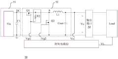
图2示出根据本发明第一实施例的充电电路的示意性框图。如图2所示,充电电路20包括直流源21、功率变换器22、控制电路23、输出端口24以及泄放电路。FIG. 2 shows a schematic block diagram of a charging circuit according to a first embodiment of the present invention. As shown in FIG. 2 , the chargingcircuit 20 includes aDC source 21 , apower converter 22 , a control circuit 23 , anoutput port 24 and a discharge circuit.

其中,直流源21提供直流供电电压DC。在本实施例中,直流源21包括直流源单元21a和第一电容C1,直流源单元21a将交流输入电压转换成直流供电电压DC,第一电容C1对直流源单元21a输出的直流供电电压DC进行滤波。直流供电电压DC例如为5V,但并不局限于此。TheDC source 21 provides a DC power supply voltage DC. In this embodiment, theDC source 21 includes aDC source unit 21a and a first capacitor C1, theDC source unit 21a converts the AC input voltage into a DC power supply voltage DC, and the first capacitor C1 supplies the DC power supply voltage DC output by theDC source unit 21a filter. The DC power supply voltage DC is, for example, 5V, but not limited thereto.

功率变换器22与所述直流源21相连接,将所述直流供电电压DC转换成输出电压Vo。功率变换器包括输出电容Cout,连接在输出端口24的第一端和第二端之间。在本实施例中,功率变换器为buck电路。Thepower converter 22 is connected to theDC source 21 and converts the DC supply voltage DC into an output voltage Vo. The power converter includes an output capacitor Cout connected between the first end and the second end of theoutput port 24 . In this embodiment, the power converter is a buck circuit.

控制电路23与负载Load和功率变换器22连接,根据负载Load的状态信号VL以及所述输出电压Vo产生所述功率变换器22的开关控制信号以调节输出电压Vo。其中,所述负载Load的状态信号VL表征所述输出端口24是否连接有负载Load。在所述输出端口24连接有负载Load时,所述开关控制信号控制相应的功率变换器22产生稳定的输出电压Vo。The control circuit 23 is connected to the load Load and thepower converter 22, and generates a switch control signal of thepower converter 22 according to the state signal VL of the load Load and the output voltage Vo to adjust the output voltage Vo. The state signal VL of the load Load represents whether theoutput port 24 is connected to the load Load. When a load Load is connected to theoutput port 24 , the switch control signal controls thecorresponding power converter 22 to generate a stable output voltage Vo.

泄放电路为输出电容Cout提供泄放通道。在所述输出端口24没有连接负载时,输出电容Cout通过泄放电路将输出电压Vo降低至预设值。The bleeder circuit provides a bleeder channel for the output capacitor Cout. When theoutput port 24 is not connected to a load, the output capacitor Cout reduces the output voltage Vo to a preset value through a bleeder circuit.

本发明实施例提供的充电电路,在使用较简单的器件、成本少的条件下,泄放电路复用功率变换器为输出电容提供泄放通道,在输出端口连接有负载时输出稳定的输出电压,在输出端口没有连接负载时将输出电压降低至预设值,达到了与传统快充电路(即DC-DC变换电路加负载开关的组合)同样的效果。减少了电路元器件,降低损耗从而提高转换效率;同时也减小了体积,降低了成本。In the charging circuit provided by the embodiment of the present invention, under the conditions of using simpler devices and less cost, the bleeder circuit multiplexes the power converter to provide a bleeder channel for the output capacitor, and outputs a stable output voltage when the output port is connected to a load , when the output port is not connected to the load, the output voltage is reduced to the preset value, which achieves the same effect as the traditional fast charging circuit (ie, the combination of the DC-DC conversion circuit and the load switch). The circuit components are reduced, the loss is reduced and the conversion efficiency is improved; at the same time, the volume is reduced and the cost is reduced.

应理解,各种达到输出电压快速降低至预设值的功率变换器和控制电路都适用于本实施例,并不局限于说明书中描述的功率变换器和控制电路。It should be understood that all kinds of power converters and control circuits that can rapidly reduce the output voltage to a preset value are applicable to this embodiment, and are not limited to the power converters and control circuits described in the specification.

如图2所示,所述功率变换器22包括第一晶体管Q1、第二晶体管Q2、第一电感L1和输出电容Cout。其中,第一晶体管Q1和第一电感L串联连接在直流源21的第一端和输出端口24的第一端之间,输出电容Cout连接在输出端口24的第一端和第二端之间;第二晶体管Q2连接在第一晶体管Q1和第一电感L1之间的第一节点A与输出端口24的第二端之间。第一晶体管Q1的控制端和第二晶体管Q2的控制端分别与控制电路23连接。所述开关控制信号包括第一开关控制信号Vg1和第二开关控制信号Vg2。具体的,第一晶体管Q1的控制端与控制电路23连接,接收第一开关控制信号Vg1;第二晶体管Q2的控制端与控制电路23连接,接收第二开关控制信号Vg2。As shown in FIG. 2 , thepower converter 22 includes a first transistor Q1 , a second transistor Q2 , a first inductor L1 and an output capacitor Cout. The first transistor Q1 and the first inductor L are connected in series between the first end of theDC source 21 and the first end of theoutput port 24 , and the output capacitor Cout is connected between the first end and the second end of theoutput port 24 ; The second transistor Q2 is connected between the first node A between the first transistor Q1 and the first inductor L1 and the second end of theoutput port 24 . The control terminal of the first transistor Q1 and the control terminal of the second transistor Q2 are respectively connected to the control circuit 23 . The switch control signals include a first switch control signal Vg1 and a second switch control signal Vg2. Specifically, the control terminal of the first transistor Q1 is connected to the control circuit 23 and receives the first switch control signal Vg1; the control terminal of the second transistor Q2 is connected to the control circuit 23 and receives the second switch control signal Vg2.

输出端口24与所述功率变换器22相连接,并且所述输出端口24在连接有负载Load时对负载Load进行充电,在没有连接负载Load时进行放电将输出电压Vo降低至预设值。其中,在没有连接负载Load时,泄放电路复用功率变换器22,为输出电容Cout提供泄放通道,从而释放输出电容Cout上的电荷。Theoutput port 24 is connected to thepower converter 22 , and theoutput port 24 charges the load Load when the load Load is connected, and reduces the output voltage Vo to a preset value by discharging when the load Load is not connected. Wherein, when the load Load is not connected, the bleeder circuit multiplexes thepower converter 22 to provide a bleeder channel for the output capacitor Cout, thereby releasing the charge on the output capacitor Cout.

所述泄放电路包括第一电感L1、第一晶体管Q1和第一电容C1,其中,第一电容C1连接在直流源21的第一端和第二端之间;输出电容Cout上的电荷依次流经第一电感L1、第一晶体管Q1和第一电容C1形成泄放回路。The discharge circuit includes a first inductor L1, a first transistor Q1 and a first capacitor C1, wherein the first capacitor C1 is connected between the first end and the second end of theDC source 21; the charges on the output capacitor Cout are sequentially The discharge loop is formed by flowing through the first inductor L1, the first transistor Q1 and the first capacitor C1.

或者,所述泄放电路包括第一电感L1和第二晶体管Q2,输出电容Cout上的电荷依次流经第一电感L1和第二晶体管Q2形成泄放回路。Alternatively, the bleeder circuit includes a first inductor L1 and a second transistor Q2, and the charge on the output capacitor Cout flows through the first inductor L1 and the second transistor Q2 in sequence to form a bleeder loop.

在输出端口24没有连接负载时,第一开关控制信号Vg1控制第一晶体管Q1处于同步整流或者关断状态,第二开关控制信号Vg2控制第二晶体管Q2交替导通和关断,使功率变换器22与直流源21断开,在第二晶体管Q2导通时,输出电容Cout上的电荷依次流经第一电感L1和第二晶体管Q2形成泄放回路,使得所述输出电压Vo降低至预设值;在第二晶体管Q2关断时,输出电容Cout上的电荷依次流经第一电感L1、第一晶体管Q1和第一电容C1形成泄放回路。在第一晶体管Q1关断时,第一晶体管Q1通过其体二极管反向续流。When theoutput port 24 is not connected to a load, the first switch control signal Vg1 controls the first transistor Q1 to be in a synchronous rectification or off state, and the second switch control signal Vg2 controls the second transistor Q2 to be turned on and off alternately, so that thepower converter 22 is disconnected from theDC source 21. When the second transistor Q2 is turned on, the charge on the output capacitor Cout flows through the first inductor L1 and the second transistor Q2 in turn to form a discharge loop, so that the output voltage Vo is reduced to a preset value. When the second transistor Q2 is turned off, the charge on the output capacitor Cout flows through the first inductor L1, the first transistor Q1 and the first capacitor C1 in sequence to form a discharge loop. When the first transistor Q1 is turned off, the first transistor Q1 reversely freewheels through its body diode.

在优选的实施例中,在输出端口24没有连接负载时,第一开关控制信号Vg1控制第一晶体管Q1处于关断状态使功率变换器22与直流源21断开,第二开关控制信号Vg2控制第二晶体管Q2工作在恒流区,输出电容Cout上的电荷依次流经第一电感L1和二晶体管Q2形成泄放回路,使得所述输出电压Vo降低至预设值。In a preferred embodiment, when theoutput port 24 is not connected to a load, the first switch control signal Vg1 controls the first transistor Q1 to be in an off state to disconnect thepower converter 22 from theDC source 21, and the second switch control signal Vg2 controls The second transistor Q2 works in the constant current region, and the charge on the output capacitor Cout flows through the first inductor L1 and the second transistor Q2 in sequence to form a bleeder loop, so that the output voltage Vo is reduced to a preset value.

在优选的实施例中,在输出端口24没有连接负载时,第一开关控制信号Vg1控制第一晶体管Q1处于关断状态使功率变换器22与直流源21断开,第二开关控制信号Vg2控制第二晶体管Q2处于导通状态,输出电容Cout上的电荷依次流经第一电感L1和二晶体管Q2形成泄放回路,使得所述输出电压Vo降低至预设值。In a preferred embodiment, when theoutput port 24 is not connected to a load, the first switch control signal Vg1 controls the first transistor Q1 to be in an off state to disconnect thepower converter 22 from theDC source 21, and the second switch control signal Vg2 controls The second transistor Q2 is in an on state, and the charges on the output capacitor Cout sequentially flow through the first inductor L1 and the second transistor Q2 to form a bleeder loop, so that the output voltage Vo is reduced to a preset value.

图4示出图1所示的充电电路的示例性工作波形图。如图4所示,在t0时刻,负载Load移除,输出端口24此时没有连接负载Load,负载Load的状态信号VL由高电平变为低电平,第一开关控制信号Vg1由高电平变为低电平,第一晶体管Q1关断,且在t0-t3期间,负载Load的状态信号VL维持为低电平,第一开关控制信号Vg1保持低电平,第一晶体管Q1始终关断。在t0时刻,第二开关控制信号Vg2由低电平变为高电平,第二晶体管Q2导通,输出电容Cout经由第二晶体管Q2放电,第二晶体管Q2的电流IQ2反向上升。t1时刻,第二开关控制信号Vg2由高电平变为低电平,第二晶体管Q2关断,第二晶体管Q2的电流IQ2降低至0,此时输出电容Cout上的电荷经由第一电感L1和第一晶体管Q1向第一电容C1充电,第一晶体管Q1体二极管续流。t2时刻,第二开关控制信号Vg2由低电平变为高电平,第二晶体管Q2重新导通。t2-t3期间,第二晶体管Q2周期性导通与关断,直至输出电容Cout放电完毕。t3时刻,检测到输出端口24连接有负载Load,负载Load的状态信号VL由低电平变为高电平,第二开关控制信号Vg2由高电平变为低电平,第二晶体管Q2关断,第一开关控制信号Vg1由低电平变为高电平,第一晶体管Q1导通,第一晶体管Q1的电流IQ1上升,直流源21的能量经由第一晶体管Q1和第一电感L1传输到负载Load。t4时刻,第一开关控制信号Vg1由高电平变为低电平,第二开关控制信号Vg2由低电平变为高电平,第一晶体管Q1关断,第二晶体管Q2导通,第一晶体管Q1的电流IQ1降低至0,第一电感L1的电流经由负载Load和第二晶体管Q2续流。t5时刻,第一开关控制信号Vg1再次变为高电平,第二开关控制信号Vg2变为低电平,第一晶体管Q1导通,第二晶体管Q2关断。t3-t6期间,第一晶体管Q1和第二晶体管Q2交替导通。t6时刻,负载Load移除,输出端口24此时没有连接负载Load,负载Load的状态信号VL由高电平变为低电平,第一开关控制信号Vg1由高电平变为低电平,第二开关控制信号Vg2由低电平变为高电平。FIG. 4 shows an exemplary operating waveform diagram of the charging circuit shown in FIG. 1 . As shown in FIG. 4 , at time t0, the load Load is removed, theoutput port 24 is not connected to the load Load at this time, the status signal VL of the load Load changes from high level to low level, and the first switch control signal Vg1 changes from high level. When the level changes to a low level, the first transistor Q1 is turned off, and during the period t0-t3, the status signal VL of the load Load is maintained at a low level, the first switch control signal Vg1 is maintained at a low level, and the first transistor Q1 is always off break. At time t0, the second switch control signal Vg2 changes from low level to high level, the second transistor Q2 is turned on, the output capacitor Cout is discharged through the second transistor Q2, and the current IQ2 of the second transistor Q2 rises in reverse. At time t1, the second switch control signal Vg2 changes from high level to low level, the second transistor Q2 is turned off, the current IQ2 of the second transistor Q2 is reduced to 0, and the charge on the output capacitor Cout passes through the first inductor L1 at this time. And the first transistor Q1 charges the first capacitor C1, and the body diode of the first transistor Q1 freewheels. At time t2, the second switch control signal Vg2 changes from a low level to a high level, and the second transistor Q2 is turned on again. During the period from t2 to t3, the second transistor Q2 is periodically turned on and off until the output capacitor Cout is completely discharged. At time t3, it is detected that theoutput port 24 is connected to the load Load, the state signal VL of the load Load changes from low level to high level, the second switch control signal Vg2 changes from high level to low level, and the second transistor Q2 is turned off. is turned off, the first switch control signal Vg1 changes from low level to high level, the first transistor Q1 is turned on, the current IQ1 of the first transistor Q1 rises, and the energy of theDC source 21 is transmitted through the first transistor Q1 and the first inductor L1 to load Load. At time t4, the first switch control signal Vg1 changes from a high level to a low level, the second switch control signal Vg2 changes from a low level to a high level, the first transistor Q1 is turned off, the second transistor Q2 is turned on, and the first transistor Q1 is turned off. The current IQ1 of a transistor Q1 is reduced to 0, and the current of the first inductor L1 is freewheeling through the load Load and the second transistor Q2. At time t5, the first switch control signal Vg1 becomes a high level again, the second switch control signal Vg2 becomes a low level, the first transistor Q1 is turned on, and the second transistor Q2 is turned off. During the period from t3 to t6, the first transistor Q1 and the second transistor Q2 are alternately turned on. At time t6, the load Load is removed, theoutput port 24 is not connected to the load Load at this time, the status signal VL of the load Load changes from high level to low level, and the first switch control signal Vg1 changes from high level to low level, The second switch control signal Vg2 changes from a low level to a high level.

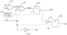
图3示出根据本发明第一实施例的充电电路中控制电路的示意性框图。如图3所示,控制电路23包括运算放大器231、锯齿波产生模块232、比较器233、第一逻辑模块234、PWM发生模块235、第二逻辑模块236、第三逻辑模块237和第四逻辑模块238。FIG. 3 shows a schematic block diagram of a control circuit in the charging circuit according to the first embodiment of the present invention. As shown in FIG. 3 , the control circuit 23 includes anoperational amplifier 231 , a sawtoothwave generation module 232 , acomparator 233 , afirst logic module 234 , aPWM generation module 235 , asecond logic module 236 , athird logic module 237 and a fourthlogic module module 238.

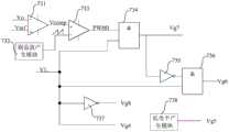
其中,运算放大器231与所述输出端口24相连接以获得所述输出电压Vo的采样信号,将所述输出电压Vo的采样信号与参考电压Vref相比得到误差信号Vcomp;锯齿波产生模块232提供锯齿波信号;比较器233与所述运算放大器231和所述锯齿波产生模块232连接,根据所述误差信号Vcomp和所述锯齿波信号产生第一PWM控制信号PWM1;第一逻辑模块234与所述负载Load和所述比较器233相连接,根据所述负载Load的状态信号VL和第一PWM控制信号PWM1产生第一开关控制信号Vg1。PWM发生模块235提供第二PWM控制信号PWM2;第二逻辑模块236与所述负载Load连接,根据所述负载Load的状态信号VL产生第一逻辑信号;第三逻辑模块237与所述第二逻辑模块236和所述PWM发生模块235连接,根据所述第一逻辑信号和第二PWM控制信号PWM2产生第二逻辑信号;第四逻辑模块238与所述第一逻辑模块234和第三逻辑模块237连接,根据第一开关控制信号Vg1和第二逻辑信号产生第二开关控制信号Vg2。Theoperational amplifier 231 is connected to theoutput port 24 to obtain the sampling signal of the output voltage Vo, and the error signal Vcomp is obtained by comparing the sampling signal of the output voltage Vo with the reference voltage Vref; the sawtoothwave generating module 232 provides a sawtooth wave signal; thecomparator 233 is connected to theoperational amplifier 231 and the sawtoothwave generating module 232, and generates a first PWM control signal PWM1 according to the error signal Vcomp and the sawtooth wave signal; thefirst logic module 234 is connected to the The load Load is connected to thecomparator 233, and a first switch control signal Vg1 is generated according to the state signal VL of the load Load and the first PWM control signal PWM1. ThePWM generation module 235 provides the second PWM control signal PWM2; thesecond logic module 236 is connected to the load Load, and generates a first logic signal according to the state signal VL of the load Load; thethird logic module 237 is connected to the second logic module Themodule 236 is connected to thePWM generating module 235, and generates a second logic signal according to the first logic signal and the second PWM control signal PWM2; thefourth logic module 238 is connected to thefirst logic module 234 and thethird logic module 237 connected to generate a second switch control signal Vg2 according to the first switch control signal Vg1 and the second logic signal.

在本实施例中,第一逻辑模块234为与门,第二逻辑模块236为非门,第三逻辑模块237为与门,第四逻辑模块238为或非门。In this embodiment, thefirst logic module 234 is an AND gate, thesecond logic module 236 is a NOT gate, thethird logic module 237 is an AND gate, and thefourth logic module 238 is a NOR gate.

在输出端口24连接有负载时,第一开关控制信号Vg1和第二开关控制信号Vg2相位相反,分别控制第一晶体管Q1和第二晶体管Q2交替导通与关断,从而保持输出电压Vo的稳定性,即功率变换器22产生稳定的输出电压Vo,以向负载Load充电。When theoutput port 24 is connected to a load, the first switch control signal Vg1 and the second switch control signal Vg2 are in opposite phases, respectively controlling the first transistor Q1 and the second transistor Q2 to be turned on and off alternately, thereby maintaining the stability of the output voltage Vo In other words, thepower converter 22 generates a stable output voltage Vo to charge the load Load.

图5示出根据本发明第二实施例的充电电路的示意性框图。充电电路30包括直流源31、功率变换器32、控制电路33、输出端口34以及泄放电路。FIG. 5 shows a schematic block diagram of a charging circuit according to a second embodiment of the present invention. The chargingcircuit 30 includes aDC source 31 , apower converter 32 , a control circuit 33 , anoutput port 34 and a discharge circuit.

与第一实施例的充电电路相比,根据第二实施例的充电电路30的主要区别在于,泄放电路包括第一电感L1、第一电阻R1和第三晶体管Q3,输出电容Cout上的电荷依次流经第一电感L1、第一电阻R1和第三晶体管Q3形成泄放回路。功率变换器32包括第一晶体管Q1、第二晶体管Q2、第一电感L1和输出电容Cout其中,第一晶体管Q1和第一电感L串联连接在直流源31的第一端和输出端口34的第一端,输出电容Cout连接在输出端口34的第一端和第二端之间;第二晶体管Q2连接在第一晶体管Q1和第一电感L1之间的第一节点A与输出端口34的第二端之间;第一电阻R1和第三晶体管Q3串联连接在第一节点A与输出端口34的第二端之间。第一晶体管Q1的控制端、第二晶体管Q2的控制端和第三晶体管Q3的控制端分别与控制电路33连接。Compared with the charging circuit of the first embodiment, the main difference of the chargingcircuit 30 according to the second embodiment is that the discharge circuit includes a first inductor L1, a first resistor R1 and a third transistor Q3, and outputs the charge on the capacitor Cout. The discharge loop is formed by flowing through the first inductor L1, the first resistor R1 and the third transistor Q3 in sequence. Thepower converter 32 includes a first transistor Q1, a second transistor Q2, a first inductor L1 and an output capacitor Cout, wherein the first transistor Q1 and the first inductor L are connected in series between the first end of theDC source 31 and the first end of theoutput port 34. One end, the output capacitor Cout is connected between the first end and the second end of theoutput port 34; the second transistor Q2 is connected between the first node A between the first transistor Q1 and the first inductor L1 and the first node A of theoutput port 34 Between the two terminals; the first resistor R1 and the third transistor Q3 are connected in series between the first node A and the second terminal of theoutput port 34 . The control terminal of the first transistor Q1 , the control terminal of the second transistor Q2 and the control terminal of the third transistor Q3 are respectively connected to the control circuit 33 .

所述开关控制信号包括第一开关控制信号Vg1、第二开关控制信号Vg2和第三开关控制信号Vg3。具体的,第一晶体管Q1的控制端与控制电路33连接,接收第一开关控制信号Vg1;第二晶体管Q2的控制端与控制电路33连接,接收第二开关控制信号Vg2,第三晶体管Q3的控制端与控制电路33连接,接收第二开关控制信号Vg3。The switch control signals include a first switch control signal Vg1, a second switch control signal Vg2 and a third switch control signal Vg3. Specifically, the control terminal of the first transistor Q1 is connected to the control circuit 33 and receives the first switch control signal Vg1; the control terminal of the second transistor Q2 is connected to the control circuit 33 and receives the second switch control signal Vg2, and the third transistor Q3 has a control terminal. The control terminal is connected to the control circuit 33 and receives the second switch control signal Vg3.

输出端口34与所述功率变换器32相连接,并且所述输出端口34在连接有负载Load时对负载Load进行充电,在没有连接负载Load时进行放电将输出电压Vo降低至预设值。在没有连接负载Load时,泄放电路复用功率变换器32,为输出电容Cout提供泄放通道,从而释放输出电容Cout上的电荷。Theoutput port 34 is connected to thepower converter 32 , and theoutput port 34 charges the load Load when the load Load is connected, and reduces the output voltage Vo to a preset value by discharging when the load Load is not connected. When the load Load is not connected, the bleeder circuit reuses thepower converter 32 to provide a bleeder channel for the output capacitor Cout, thereby releasing the charge on the output capacitor Cout.

在输出端口34连接有负载Load时,第一开关控制信号Vg1和第二开关控制信号Vg2的相位相反,分别控制第一晶体管Q1和第二晶体管Q2交替导通与关断,第三开关控制信号Vg3控制第三晶体管Q3处于关断状态,从而保持输出电压Vo的稳定性,即功率变换器32产生稳定的输出电压Vo,以向负载Load充电。When theoutput port 34 is connected to the load Load, the phases of the first switch control signal Vg1 and the second switch control signal Vg2 are opposite, respectively controlling the first transistor Q1 and the second transistor Q2 to be turned on and off alternately, and the third switch control signal Vg3 controls the third transistor Q3 to be in an off state, so as to maintain the stability of the output voltage Vo, that is, thepower converter 32 generates a stable output voltage Vo to charge the load Load.

具体地,在输出端口34连接有负载Load时,第一晶体管Q1导通,第二晶体管Q2和第三晶体管Q3关断,功率变换器32的电流经由直流源31的第一端流经第一晶体管Q1、第一电感L1、负载Load,最后流向地,第二晶体管Q2导通时,第一晶体管Q1和第三晶体管Q3关断,第一电感L1上的电流不能突变,第一电感L1上的电流经由负载Load和第二晶体管Q2,然后回到第一电感L1,形成一个续流回路。Specifically, when theoutput port 34 is connected to the load Load, the first transistor Q1 is turned on, the second transistor Q2 and the third transistor Q3 are turned off, and the current of thepower converter 32 flows through the first end of theDC source 31 through the first The transistor Q1, the first inductor L1, and the load Load finally flow to the ground. When the second transistor Q2 is turned on, the first transistor Q1 and the third transistor Q3 are turned off, and the current on the first inductor L1 cannot change abruptly. The current passes through the load Load and the second transistor Q2, and then returns to the first inductor L1 to form a freewheeling loop.

在输出端口34移除负载Load时,第一晶体管Q1和第二晶体管Q2关断从而切断前级电压,同时第三晶体管Q3导通,输出电容Cout上的电荷依次流经第一电感L1、第一电阻R1和第三晶体管Q3形成泄放回路,使得输出电压Vo下降至预设值。When the load Load is removed from theoutput port 34, the first transistor Q1 and the second transistor Q2 are turned off to cut off the previous stage voltage, while the third transistor Q3 is turned on, and the charge on the output capacitor Cout flows through the first inductor L1, the first A resistor R1 and the third transistor Q3 form a bleeder loop, so that the output voltage Vo drops to a preset value.

具体地,在输出端口34没有连接负载Load时,第一开关控制信号Vg1控制第一晶体管Q1处于关断状态,第二开关控制信号Vg2控制第二晶体管Q2处于关断状态,使功率变换器32与直流源31断开,第三开关控制信号Vg3控制第三晶体管Q3处于导通状态,输出电容Cout上的电荷依次流经第一电感L1、第一电阻R1和第三晶体管Q3形成泄放回路,以将所述输出电压Vo降低至预设值。Specifically, when theoutput port 34 is not connected to the load Load, the first switch control signal Vg1 controls the first transistor Q1 to be in an off state, and the second switch control signal Vg2 controls the second transistor Q2 to be in an off state, so that thepower converter 32 It is disconnected from theDC source 31, the third switch control signal Vg3 controls the third transistor Q3 to be in an on state, and the charge on the output capacitor Cout flows through the first inductor L1, the first resistor R1 and the third transistor Q3 in turn to form a discharge loop. , to reduce the output voltage Vo to a preset value.

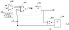
图6示出根据本发明第二实施例的充电电路中控制电路的示意性框图。如图6所示,控制电路33包括运算放大器331、锯齿波产生模块332、比较器333、第一逻辑模块334、第五逻辑模块335、第六逻辑模块336和第七逻辑模块337。6 shows a schematic block diagram of a control circuit in a charging circuit according to a second embodiment of the present invention. As shown in FIG. 6 , the control circuit 33 includes anoperational amplifier 331 , a sawtoothwave generating module 332 , acomparator 333 , afirst logic module 334 , afifth logic module 335 , asixth logic module 336 and aseventh logic module 337 .

其中,运算放大器331与所述输出端口34相连接以获得所述输出电压Vo的采样信号,将所述输出电压Vo的采样信号与参考电压Vref相比较得到误差信号Vcomp;锯齿波产生模块332提供锯齿波信号;比较器333与所述运算放大器331和所述锯齿波产生模块332连接,根据所述误差信号Vcomp和所述锯齿波信号产生第一PWM控制信号PWM1;第一逻辑模块334与所述负载Load和所述比较器333相连接,根据所述负载Load的状态信号VL和第一PWM控制信号PWM1产生第一开关控制信号Vg1。第五逻辑模块335与所述第一逻辑模块334连接,根据所述第一开关控制信号Vg1产生第五逻辑信号;第六逻辑模块336与所述第五逻辑模块335和所述负载Load连接,根据所述第五逻辑信号和所述负载Load的状态信号VL产生第二开关控制信号Vg2。第七逻辑模块337与所述负载Load连接,根据所述负载Load的状态信号VL产生第三开关控制信号Vg3。Theoperational amplifier 331 is connected to theoutput port 34 to obtain a sampling signal of the output voltage Vo, and the error signal Vcomp is obtained by comparing the sampling signal of the output voltage Vo with the reference voltage Vref; the sawtoothwave generating module 332 provides a sawtooth wave signal; thecomparator 333 is connected to theoperational amplifier 331 and the sawtoothwave generating module 332, and generates a first PWM control signal PWM1 according to the error signal Vcomp and the sawtooth wave signal; thefirst logic module 334 is connected to the The load Load is connected to thecomparator 333, and a first switch control signal Vg1 is generated according to the state signal VL of the load Load and the first PWM control signal PWM1. Thefifth logic module 335 is connected to thefirst logic module 334, and generates a fifth logic signal according to the first switch control signal Vg1; thesixth logic module 336 is connected to thefifth logic module 335 and the load Load, A second switch control signal Vg2 is generated according to the fifth logic signal and the state signal VL of the load Load. Theseventh logic module 337 is connected to the load Load, and generates a third switch control signal Vg3 according to the state signal VL of the load Load.

在本实施例中,第一逻辑模块334为与门,第五逻辑模块335为非门,第六逻辑模块336为与门,第七逻辑模块337为非门。In this embodiment, thefirst logic module 334 is an AND gate, thefifth logic module 335 is a NOT gate, thesixth logic module 336 is an AND gate, and theseventh logic module 337 is a NOT gate.

根据第二实施例的充电电路30的其余方面与第一实施例相同,因此不再详述。The remaining aspects of the chargingcircuit 30 according to the second embodiment are the same as those of the first embodiment, and thus will not be described in detail.

图7示出根据本发明第三实施例的充电电路的示意性框图。充电电路40包括直流源41、功率变换器42、控制电路43、输出端口44以及泄放电路。FIG. 7 shows a schematic block diagram of a charging circuit according to a third embodiment of the present invention. The chargingcircuit 40 includes aDC source 41 , apower converter 42 , a control circuit 43 , anoutput port 44 and a discharge circuit.

与第二实施例的充电电路相比,根据第三实施例的充电电路40的主要区别在于,泄放电路与输出电容并联连接,且泄放电路包括第一电阻R1和第三晶体管Q3,第一电阻R1和第三晶体管Q3串联连接在输出电容Cout的两端。在没有连接负载Load时,泄放电路与输出电容并联连接,为输出电容Cout提供泄放通道,从而释放输出电容Cout上的电荷。Compared with the charging circuit of the second embodiment, the main difference of the chargingcircuit 40 according to the third embodiment is that the bleeder circuit is connected in parallel with the output capacitor, and the bleeder circuit includes a first resistor R1 and a third transistor Q3, A resistor R1 and a third transistor Q3 are connected in series across the output capacitor Cout. When the load Load is not connected, the bleeder circuit is connected in parallel with the output capacitor to provide a bleeder channel for the output capacitor Cout, thereby releasing the charge on the output capacitor Cout.

在输出端口44移除负载Load时,第一晶体管Q1和第二晶体管Q2关断从而切断前级电压,同时第三晶体管Q3导通,输出电容Cout上的电荷依次流经第一电阻R1和第三晶体管Q3形成泄放回路,使得输出电压Vo下降至预设值。When the load Load is removed from theoutput port 44, the first transistor Q1 and the second transistor Q2 are turned off to cut off the previous stage voltage, while the third transistor Q3 is turned on, and the charge on the output capacitor Cout flows through the first resistor R1 and the first resistor in turn The three transistors Q3 form a bleeder loop, so that the output voltage Vo drops to a preset value.

具体地,在输出端口44没有连接负载Load时,第一开关控制信号Vg1控制第一晶体管Q1处于关断状态,第二开关控制信号Vg2控制第二晶体管Q2处于关断状态,使功率变换器42与直流源41断开,第三开关控制信号Vg3控制第三晶体管Q3处于导通状态,输出电容Cout上的电荷依次流经第一电阻R1和第三晶体管Q3形成泄放回路,以将所述输出电压Vo降低至预设值。Specifically, when theoutput port 44 is not connected to the load Load, the first switch control signal Vg1 controls the first transistor Q1 to be in an off state, and the second switch control signal Vg2 controls the second transistor Q2 to be in an off state, so that thepower converter 42 It is disconnected from theDC source 41, the third switch control signal Vg3 controls the third transistor Q3 to be in an on state, and the charge on the output capacitor Cout flows through the first resistor R1 and the third transistor Q3 in turn to form a discharge loop, so as to discharge the The output voltage Vo is reduced to a preset value.

根据第三实施例的充电电路40的其余方面与第二实施例相同,因此不再详述。The remaining aspects of the chargingcircuit 40 according to the third embodiment are the same as those of the second embodiment, and thus will not be described in detail.

图8示出根据本发明第四实施例的充电电路的示意性框图。充电电路50包括直流源51、功率变换器52、控制电路53、输出端口54、以及泄放电路。FIG. 8 shows a schematic block diagram of a charging circuit according to a fourth embodiment of the present invention. The chargingcircuit 50 includes aDC source 51, apower converter 52, a control circuit 53, an output port 54, and a discharge circuit.

与第一实施例的充电电路相比,根据第四实施例的充电电路50的主要区别在于,所述泄放电路包括第一电感L1和第二电阻R2,输出电容Cout上的电荷依次流经第一电感L1和第二电阻R2形成泄放回路。功率变换器52包括第一晶体管Q1、第二晶体管Q2、第一电感L1和输出电容Cout。Compared with the charging circuit of the first embodiment, the main difference of the chargingcircuit 50 according to the fourth embodiment is that the bleeder circuit includes a first inductor L1 and a second resistor R2, and the charges on the output capacitor Cout flow through in sequence. The first inductor L1 and the second resistor R2 form a bleeder loop. Thepower converter 52 includes a first transistor Q1, a second transistor Q2, a first inductor L1 and an output capacitor Cout.

其中,第一晶体管Q1和第一电感L串联连接在直流源51的第一端和输出端口54的第一端,输出电容Cout连接在输出端口54的第一端和第二端之间;第二晶体管Q2连接在第一晶体管Q1和第一电感L1之间的第一节点A与输出端口54的第二端之间;第二电阻R2连接第一节点A与第一晶体管Q1的控制端之间。第一晶体管Q1的控制端和第二晶体管Q2的控制端分别与控制电路53连接。The first transistor Q1 and the first inductor L are connected in series between the first end of theDC source 51 and the first end of the output port 54, and the output capacitor Cout is connected between the first end and the second end of the output port 54; The two transistors Q2 are connected between the first node A between the first transistor Q1 and the first inductor L1 and the second terminal of the output port 54; the second resistor R2 is connected between the first node A and the control terminal of the first transistor Q1 between. The control terminal of the first transistor Q1 and the control terminal of the second transistor Q2 are respectively connected to the control circuit 53 .

所述开关控制信号包括第一开关控制信号Vg1和第二开关控制信号Vg2。具体的,第一晶体管Q1的控制端与控制电路53连接,接收第一开关控制信号Vg1;第二晶体管Q2的控制端与控制电路53连接,接收第二开关控制信号Vg2。The switch control signals include a first switch control signal Vg1 and a second switch control signal Vg2. Specifically, the control terminal of the first transistor Q1 is connected to the control circuit 53 and receives the first switch control signal Vg1; the control terminal of the second transistor Q2 is connected to the control circuit 53 and receives the second switch control signal Vg2.

输出端口54与所述功率变换器52相连接,并且所述输出端口54在连接有负载Load时对负载Load进行充电,在没有连接负载Load时进行放电将输出电压Vo降低至预设值。在没有连接负载Load时,泄放电路复用功率变换器52,为输出电容Cout提供泄放通道,从而释放输出电容Cout上的电荷。The output port 54 is connected to thepower converter 52 , and the output port 54 charges the load Load when the load Load is connected, and reduces the output voltage Vo to a preset value by discharging when the load Load is not connected. When the load Load is not connected, the bleeder circuit reuses thepower converter 52 to provide a bleeder channel for the output capacitor Cout, thereby releasing the charge on the output capacitor Cout.

在输出端口54连接有负载Load时,第一开关控制信号Vg1和第二开关控制信号Vg2的相位相反,分别控制第一晶体管Q1和第二晶体管Q2交替导通与关断,从而保持输出电压Vo的稳定性,即功率变换器52产生稳定的输出电压Vo,以向负载Load充电。具体地,在输出端口54连接有负载Load时,第一晶体管Q1导通,第二晶体管Q2关断,电流经由直流源51的第一端流经第一晶体管Q1、第一电感L1、负载Load,最后流向地,形成供电回路,第二晶体管Q2导通时,第一晶体管Q1关断,第一电感L1上的电流不能突变,第一电感L1上的电流经由负载Load和第二晶体管Q2,然后回到第一电感L1,形成一个续流回路。When the output port 54 is connected to the load Load, the phases of the first switch control signal Vg1 and the second switch control signal Vg2 are opposite, respectively controlling the first transistor Q1 and the second transistor Q2 to be turned on and off alternately, thereby maintaining the output voltage Vo stability, that is, thepower converter 52 generates a stable output voltage Vo to charge the load Load. Specifically, when the output port 54 is connected to the load Load, the first transistor Q1 is turned on, the second transistor Q2 is turned off, and the current flows through the first transistor Q1 , the first inductor L1 , and the load Load through the first end of theDC source 51 . , and finally flows to the ground to form a power supply loop. When the second transistor Q2 is turned on, the first transistor Q1 is turned off, and the current on the first inductor L1 cannot change abruptly. The current on the first inductor L1 passes through the load Load and the second transistor Q2. Then return to the first inductor L1 to form a freewheeling loop.

在输出端口54没有连接负载时,第一开关控制信号Vg1控制第一晶体管Q1处于关断状态,第二开关控制信号Vg2控制第二晶体管Q2处于关断状态,使功率变换器52与直流源51断开,并将功率变换器52的输出电压Vo降低至预设值。具体地,在输出端口54移除负载Load时,第一晶体管Q1和第二晶体管Q2关断从而切断前级电压,输出电容Cout上的电荷依次流经第一电感L1和第二电阻R2形成泄放回路,使得输出电压Vo下降至预设值。When the output port 54 is not connected to a load, the first switch control signal Vg1 controls the first transistor Q1 to be in an off state, and the second switch control signal Vg2 controls the second transistor Q2 to be in an off state, so that thepower converter 52 is connected to theDC source 51 Disconnect and reduce the output voltage Vo of thepower converter 52 to a preset value. Specifically, when the load Load is removed from the output port 54, the first transistor Q1 and the second transistor Q2 are turned off to cut off the previous stage voltage, and the charge on the output capacitor Cout flows through the first inductor L1 and the second resistor R2 in turn to form a leakage put the loop, so that the output voltage Vo drops to the preset value.

图9示出根据本发明第四实施例的充电电路中控制电路的示意性框图。如图9所示,控制电路43包括运算放大器531、锯齿波产生模块532、比较器533、第一逻辑模块534、第五逻辑模块535和第六逻辑模块536。9 shows a schematic block diagram of a control circuit in a charging circuit according to a fourth embodiment of the present invention. As shown in FIG. 9 , the control circuit 43 includes anoperational amplifier 531 , a sawtoothwave generating module 532 , acomparator 533 , afirst logic module 534 , afifth logic module 535 and asixth logic module 536 .

其中,运算放大器531与所述输出端口54相连接以获得所述输出电压Vo的采样信号,将所述输出电压Vo的采样信号与参考电压Vref相比较得到误差信号Vcomp;锯齿波产生模块532提供锯齿波信号;比较器533与所述运算放大器531和所述锯齿波产生模块532连接,根据所述误差信号Vcomp和所述锯齿波信号产生第一PWM控制信号PWM1;第一逻辑模块534与所述负载Load和所述比较器533相连接,根据所述负载Load的状态信号VL和第一PWM控制信号PWM1产生第一开关控制信号Vg1。第五逻辑模块535与所述第一逻辑模块534连接,根据所述第一开关控制信号Vg1产生第五逻辑信号;第六逻辑模块536与所述第五逻辑模块535和所述负载Load连接,根据所述第五逻辑信号和所述负载Load的状态信号VL产生第二开关控制信号Vg2。Theoperational amplifier 531 is connected to the output port 54 to obtain the sampling signal of the output voltage Vo, and the error signal Vcomp is obtained by comparing the sampling signal of the output voltage Vo with the reference voltage Vref; the sawtoothwave generating module 532 provides a sawtooth wave signal; thecomparator 533 is connected to theoperational amplifier 531 and the sawtoothwave generating module 532, and generates a first PWM control signal PWM1 according to the error signal Vcomp and the sawtooth wave signal; thefirst logic module 534 is connected to the The load Load is connected to thecomparator 533, and a first switch control signal Vg1 is generated according to the state signal VL of the load Load and the first PWM control signal PWM1. Thefifth logic module 535 is connected to thefirst logic module 534, and generates a fifth logic signal according to the first switch control signal Vg1; thesixth logic module 536 is connected to thefifth logic module 535 and the load Load, A second switch control signal Vg2 is generated according to the fifth logic signal and the state signal VL of the load Load.

在本实施例中,第一逻辑模块534为与门,第五逻辑模块535为非门,第六逻辑模块536为与门。In this embodiment, thefirst logic module 534 is an AND gate, thefifth logic module 535 is a NOT gate, and thesixth logic module 536 is an AND gate.

根据第四实施例的充电电路50的其余方面与第一实施例相同,因此不再详述。The remaining aspects of the chargingcircuit 50 according to the fourth embodiment are the same as those of the first embodiment, and thus will not be described in detail.

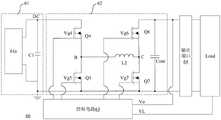
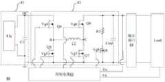
图10示出根据本发明第五实施例的充电电路的示意性框图。充电电路60包括直流源61、功率变换器62、控制电路63、输出端口64以及泄放电路。FIG. 10 shows a schematic block diagram of a charging circuit according to a fifth embodiment of the present invention. The chargingcircuit 60 includes aDC source 61 , apower converter 62 , a control circuit 63 , anoutput port 64 and a discharge circuit.

与第一实施例的充电电路相比,根据第五实施例的充电电路60的主要区别在于,所述泄放电路包括第六晶体管Q6、第二电感L2、第四晶体管Q4和第一电容C1;输出电容Cout上的电荷依次流经第六晶体管Q6、第二电感L2、第四晶体管Q4和第一电容C1形成泄放回路。或者,所述泄放电路包括第六晶体管Q6、第二电感L2和第五晶体管Q5,输出电容Cout上的电荷依次流经第六晶体管Q6、第二电感L2和第五晶体管Q5形成泄放回路。或者,所述泄放电路包括第六晶体管Q6和第七晶体管Q7,输出电容Cout上的电荷依次流经第六晶体管Q6和第七晶体管Q7形成泄放回路。功率变换器62包括第四晶体管至第七晶体管(Q4-Q7)、第二电感L2和输出电容Cout。在本实施例中,功率变换器为升降压电路。Compared with the charging circuit of the first embodiment, the main difference of the chargingcircuit 60 according to the fifth embodiment is that the discharge circuit includes a sixth transistor Q6, a second inductor L2, a fourth transistor Q4 and a first capacitor C1 ; The charge on the output capacitor Cout sequentially flows through the sixth transistor Q6, the second inductor L2, the fourth transistor Q4 and the first capacitor C1 to form a discharge loop. Alternatively, the bleeder circuit includes a sixth transistor Q6, a second inductor L2 and a fifth transistor Q5, and the charge on the output capacitor Cout flows through the sixth transistor Q6, the second inductor L2 and the fifth transistor Q5 in sequence to form a bleeder loop . Alternatively, the discharge circuit includes a sixth transistor Q6 and a seventh transistor Q7, and the charges on the output capacitor Cout flow through the sixth transistor Q6 and the seventh transistor Q7 in sequence to form a discharge loop. Thepower converter 62 includes fourth to seventh transistors ( Q4 - Q7 ), a second inductor L2 and an output capacitor Cout. In this embodiment, the power converter is a buck-boost circuit.

其中,第四晶体管Q4和第五晶体管Q5串联连接在直流源61的第一端和第二端之间;所述第六晶体管Q6和第七晶体管Q7串联连接在输出端口64的第一端和第二端之间;第二电感L2连接在第四晶体管Q4和第五晶体管Q5之间的第二节点B与所述第六晶体管Q6和第七晶体管Q7之间的第三节点C之间;所述输出电容Cout连接在输出端口64的第一端和第二端之间。第四晶体管Q4的控制端、第五晶体管Q5的控制端、第六晶体管Q6的控制端和第七晶体管Q7的控制端分别与控制电路63连接。The fourth transistor Q4 and the fifth transistor Q5 are connected in series between the first end and the second end of theDC source 61; the sixth transistor Q6 and the seventh transistor Q7 are connected in series between the first end and the second end of theoutput port 64. between the second ends; the second inductor L2 is connected between the second node B between the fourth transistor Q4 and the fifth transistor Q5 and the third node C between the sixth transistor Q6 and the seventh transistor Q7; The output capacitor Cout is connected between the first end and the second end of theoutput port 64 . The control terminal of the fourth transistor Q4, the control terminal of the fifth transistor Q5, the control terminal of the sixth transistor Q6 and the control terminal of the seventh transistor Q7 are respectively connected to the control circuit 63.

所述开关控制信号包括第四开关控制信号Vg4、第五开关控制信号Vg5、第六开关控制信号Vg6和第七开关控制信号Vg7。第四晶体管Q4的控制端与控制电路63连接,接收第四开关控制信号Vg4;第五晶体管Q5的控制端与控制电路63连接,接收第五开关控制信号Vg5;第六晶体管Q6的控制端与控制电路63连接,接收第六开关控制信号Vg6;第七晶体管Q7的控制端与控制电路63连接,接收第七开关控制信号Vg7。The switch control signals include a fourth switch control signal Vg4, a fifth switch control signal Vg5, a sixth switch control signal Vg6 and a seventh switch control signal Vg7. The control terminal of the fourth transistor Q4 is connected to the control circuit 63 to receive the fourth switch control signal Vg4; the control terminal of the fifth transistor Q5 is connected to the control circuit 63 to receive the fifth switch control signal Vg5; the control terminal of the sixth transistor Q6 is connected to the control circuit 63. The control circuit 63 is connected to receive the sixth switch control signal Vg6; the control end of the seventh transistor Q7 is connected to the control circuit 63 and receives the seventh switch control signal Vg7.

输出端口64与所述功率变换器62相连接,并且所述输出端口64在连接有负载Load时对负载Load进行充电,具体地,在所述输出端口64连接有负载Load时,第四晶体管至第七晶体管(Q4-Q7)在控制电路63的控制下使得所述功率变换器62工作在降压模式、升压模式以及升降压模式。具体地,当所述功率变换器62工作在降压模式时,第四开关控制信号Vg4和第五开关控制信号Vg5分别控制第四晶体管Q4和第五晶体管Q5交替导通,第六开关控制信号Vg6控制第六晶体管Q6处于导通状态,第七开关控制信号Vg7控制第七晶体管Q7处于关断状态。当所述功率变换器62工作在升压模式时,第四开关控制信号Vg4控制第四晶体管Q4处于导通状态,第五开关控制信号Vg5控制第五晶体管Q5处于关断状态,第六开关控制信号Vg6和第七开关控制信号Vg7分别控制第六晶体管Q6和第七晶体管Q7交替导通。当所述功率变换器62工作在升降压模式时,第四控制信号Vg4、第五控制信号Vg5、第六控制信号Vg6和第七控制信号Vg7分别控制第四晶体管Q4、第五晶体管Q5、第六晶体管Q6和第七晶体管Q7交替导通。Theoutput port 64 is connected to thepower converter 62, and theoutput port 64 charges the load Load when theoutput port 64 is connected to the load Load. Specifically, when theoutput port 64 is connected to the load Load, the fourth transistor to The seventh transistors ( Q4 - Q7 ) make thepower converter 62 work in a buck mode, a boost mode and a buck-boost mode under the control of the control circuit 63 . Specifically, when thepower converter 62 operates in the step-down mode, the fourth switch control signal Vg4 and the fifth switch control signal Vg5 respectively control the fourth transistor Q4 and the fifth transistor Q5 to be turned on alternately, and the sixth switch control signal Vg6 controls the sixth transistor Q6 to be in an on state, and the seventh switch control signal Vg7 controls the seventh transistor Q7 to be in an off state. When thepower converter 62 works in the boost mode, the fourth switch control signal Vg4 controls the fourth transistor Q4 to be in an on state, the fifth switch control signal Vg5 controls the fifth transistor Q5 to be in an off state, and the sixth switch controls The signal Vg6 and the seventh switch control signal Vg7 respectively control the sixth transistor Q6 and the seventh transistor Q7 to be turned on alternately. When thepower converter 62 operates in the buck-boost mode, the fourth control signal Vg4, the fifth control signal Vg5, the sixth control signal Vg6 and the seventh control signal Vg7 control the fourth transistor Q4, the fifth transistor Q5, The sixth transistor Q6 and the seventh transistor Q7 are alternately turned on.

在没有连接负载Load时进行放电将输出电压Vo降低至预设值。在没有连接负载Load时,泄放电路复用功率变换器62,为输出电容Cout提供泄放通道,从而释放输出电容Cout上的电荷。Discharging when no load Load is connected reduces the output voltage Vo to a preset value. When the load Load is not connected, the bleeder circuit reuses thepower converter 62 to provide a bleeder channel for the output capacitor Cout, thereby releasing the charge on the output capacitor Cout.

具体地,在所述输出端口64没有连接负载Load时,第四开关控制信号Vg4控制第四晶体管Q4处于同步整流或者关断状态,第五开关控制信号Vg5控制第五晶体管Q5交替导通与关断,第六开关控制信号Vg6控制第六晶体管Q6处于导通状态,第七开关控制信号Vg7控制第七晶体管Q7处于关断状态。在第五晶体管Q5导通时,输出电容Cout上的电荷依次流经第六晶体管Q6、第二电感L2和第五晶体管Q5形成泄放回路;在第五晶体管Q5关断时,输出电容Cout上的电荷依次流经第六晶体管Q6、第二电感L2、第四晶体管Q4和第一电容C1形成泄放回路,使得输出电压Vo降低至预设值。在第四晶体管Q4关断时,第四晶体管Q4通过其体二极管反向续流。Specifically, when theoutput port 64 is not connected to the load Load, the fourth switch control signal Vg4 controls the fourth transistor Q4 to be in a synchronous rectification or off state, and the fifth switch control signal Vg5 controls the fifth transistor Q5 to be turned on and off alternately off, the sixth switch control signal Vg6 controls the sixth transistor Q6 to be in an on state, and the seventh switch control signal Vg7 controls the seventh transistor Q7 to be in an off state. When the fifth transistor Q5 is turned on, the charge on the output capacitor Cout flows through the sixth transistor Q6, the second inductor L2 and the fifth transistor Q5 in turn to form a discharge loop; when the fifth transistor Q5 is turned off, the charge on the output capacitor Cout The charge flows through the sixth transistor Q6, the second inductor L2, the fourth transistor Q4 and the first capacitor C1 in sequence to form a discharge loop, so that the output voltage Vo is reduced to a preset value. When the fourth transistor Q4 is turned off, the fourth transistor Q4 reversely freewheels through its body diode.

在优选的实施例中,在所述输出端口64没有连接负载Load时,第四开关控制信号Vg4控制第四晶体管Q4处于关断状态,第六开关控制信号Vg6控制第六晶体管Q6工作在恒流区,第五开关控制信号Vg5控制第五晶体管Q5工作在恒流区;第七开关控制信号Vg7控制第七晶体管Q7处于关断状态或工作在可变电阻区或工作在恒流区或处于导通状态。输出电容Cout上的电荷依次流经第六晶体管Q6、第二电感L2和第五晶体管Q5形成泄放回路,使得输出电压Vo降低至预设值。In a preferred embodiment, when theoutput port 64 is not connected to the load Load, the fourth switch control signal Vg4 controls the fourth transistor Q4 to be in an off state, and the sixth switch control signal Vg6 controls the sixth transistor Q6 to work at a constant current region, the fifth switch control signal Vg5 controls the fifth transistor Q5 to work in the constant current region; the seventh switch control signal Vg7 controls the seventh transistor Q7 to be in an off state or work in the variable resistance region or in the constant current region or in the conduction region pass status. The charge on the output capacitor Cout sequentially flows through the sixth transistor Q6, the second inductor L2 and the fifth transistor Q5 to form a bleeder loop, so that the output voltage Vo is reduced to a preset value.

在优选的实施例中,在所述输出端口64没有连接负载Load时,第四开关控制信号Vg4控制第四晶体管Q4处于关断状态,第六开关控制信号Vg6控制第六晶体管Q6工作在恒流区,第五开关控制信号Vg5控制第五晶体管Q5工作处于关断状态或工作在可变电阻区或工作在恒流区或处于导通状态,第七开关控制信号Vg7控制第七晶体管Q7工作在恒流区。输出电容Cout上的电荷依次流经第六晶体管Q6和第七晶体管Q7形成泄放回路,使得输出电压Vo降低至预设值。In a preferred embodiment, when theoutput port 64 is not connected to the load Load, the fourth switch control signal Vg4 controls the fourth transistor Q4 to be in an off state, and the sixth switch control signal Vg6 controls the sixth transistor Q6 to work at a constant current region, the fifth switch control signal Vg5 controls the fifth transistor Q5 to work in the off state or in the variable resistance region or in the constant current region or in the on state, the seventh switch control signal Vg7 controls the seventh transistor Q7 to work in the constant current zone. The charge on the output capacitor Cout flows through the sixth transistor Q6 and the seventh transistor Q7 in sequence to form a bleeder loop, so that the output voltage Vo is reduced to a preset value.

在优选的实施例中,在所述输出端口64没有连接负载Load时,第四开关控制信号Vg4控制第四晶体管Q4处于关断状态,第六开关控制信号Vg6控制第六晶体管Q6处于导通状态,第五开关控制信号Vg5控制第五晶体管Q5处于导通状态,第七开关控制信号Vg7控制第七晶体管Q7处于关断状态或者工作在可变电阻区。输出电容Cout上的电荷依次流经第六晶体管Q6、第二电感L2和第五晶体管Q5形成泄放回路,使得输出电压Vo降低至预设值。In a preferred embodiment, when theoutput port 64 is not connected to the load Load, the fourth switch control signal Vg4 controls the fourth transistor Q4 to be in an off state, and the sixth switch control signal Vg6 controls the sixth transistor Q6 to be in an on state , the fifth switch control signal Vg5 controls the fifth transistor Q5 to be in an on state, and the seventh switch control signal Vg7 controls the seventh transistor Q7 to be in an off state or work in the variable resistance region. The charge on the output capacitor Cout sequentially flows through the sixth transistor Q6, the second inductor L2 and the fifth transistor Q5 to form a bleeder loop, so that the output voltage Vo is reduced to a preset value.

在优选的实施例中,在所述输出端口64没有连接负载Load时,第四开关控制信号Vg4控制第四晶体管Q4处于关断状态,第六开关控制信号Vg6控制第六晶体管Q6处于导通状态,第五开关控制信号Vg5控制第五晶体管Q5处于导通状态或关断状态或工作在可变电阻区,第七开关控制信号Vg7控制第七晶体管Q7处于导通状态。输出电容Cout上的电荷依次流经第六晶体管Q6和第七晶体管Q7形成泄放回路,使得输出电压Vo降低至预设值。In a preferred embodiment, when theoutput port 64 is not connected to the load Load, the fourth switch control signal Vg4 controls the fourth transistor Q4 to be in an off state, and the sixth switch control signal Vg6 controls the sixth transistor Q6 to be in an on state , the fifth switch control signal Vg5 controls the fifth transistor Q5 to be on or off or works in the variable resistance region, and the seventh switch control signal Vg7 controls the seventh transistor Q7 to be on. The charge on the output capacitor Cout flows through the sixth transistor Q6 and the seventh transistor Q7 in sequence to form a bleeder loop, so that the output voltage Vo is reduced to a preset value.

图11示出根据本发明第五实施例的充电电路中控制电路的示意性框图。如图11所示,控制电路63包括运算放大器631、锯齿波产生模块632、比较器633、第一逻辑模块634、PWM发生模块635、第二逻辑模块636、第三逻辑模块637、第四逻辑模块638和第七逻辑模块639。FIG. 11 shows a schematic block diagram of a control circuit in a charging circuit according to a fifth embodiment of the present invention. As shown in FIG. 11 , the control circuit 63 includes anoperational amplifier 631 , a sawtoothwave generation module 632 , acomparator 633 , afirst logic module 634 , aPWM generation module 635 , asecond logic module 636 , athird logic module 637 , and a fourthlogic module module 638 andseventh logic module 639 .

其中,运算放大器631与所述输出端口64相连接以获得所述输出电压Vo的采样信号,将所述输出电压Vo的采样信号与参考电压Vref相比产生误差信号Vcomp;锯齿波产生模块632提供锯齿波信号;比较器633与所述运算放大器631和所述锯齿波产生模块632连接,根据所述误差信号Vcomp和所述锯齿波信号产生第一PWM控制信号PWM1;第七逻辑模块639与所述负载Load连接,根据所述负载Load的状态信号VL产生第五开关控制信号Vg5。第一逻辑模块634与所述负载Load和所述比较器633相连接,根据所述负载Load的状态信号VL和第一PWM控制信号PWM1产生第七开关控制信号Vg7。PWM发生模块635提供第二PWM控制信号PWM2;第二逻辑模块636与所述负载Load连接,根据所述负载Load的状态信号VL产生第一逻辑信号;第三逻辑模块637与所述第二逻辑模块636和所述PWM发生模块635连接,根据所述第一逻辑信号和第二PWM控制信号PWM2产生第二逻辑信号;第四逻辑模块638与所述第一逻辑模块634和第三逻辑模块637连接,根据第一开关控制信号Vg1和第二逻辑信号产生第六开关控制信号Vg6。所述第四开关控制信号Vg4与所述负载Load的状态信号VL一致。Theoperational amplifier 631 is connected to theoutput port 64 to obtain a sampling signal of the output voltage Vo, and compares the sampling signal of the output voltage Vo with the reference voltage Vref to generate an error signal Vcomp; the sawtoothwave generating module 632 provides a sawtooth wave signal; thecomparator 633 is connected to theoperational amplifier 631 and the sawtoothwave generating module 632, and generates a first PWM control signal PWM1 according to the error signal Vcomp and the sawtooth wave signal; theseventh logic module 639 is connected to the The load Load is connected, and a fifth switch control signal Vg5 is generated according to the state signal VL of the load Load. Thefirst logic module 634 is connected to the load Load and thecomparator 633, and generates a seventh switch control signal Vg7 according to the state signal VL of the load Load and the first PWM control signal PWM1. ThePWM generation module 635 provides the second PWM control signal PWM2; thesecond logic module 636 is connected to the load Load, and generates a first logic signal according to the state signal VL of the load Load; thethird logic module 637 is connected to the second logic module Themodule 636 is connected to thePWM generation module 635, and generates a second logic signal according to the first logic signal and the second PWM control signal PWM2; thefourth logic module 638 is connected to thefirst logic module 634 and thethird logic module 637 connected to generate a sixth switch control signal Vg6 according to the first switch control signal Vg1 and the second logic signal. The fourth switch control signal Vg4 is consistent with the state signal VL of the load Load.

在本实施例中,第一逻辑模块634为与门,第二逻辑模块636为非门,第三逻辑模块637为与门,第四逻辑模块638为或非门,第七逻辑模块639为非门。In this embodiment, thefirst logic module 634 is an AND gate, thesecond logic module 636 is a NOT gate, thethird logic module 637 is an AND gate, thefourth logic module 638 is a NOR gate, and theseventh logic module 639 is a NOT gate Door.

根据第五实施例的充电电路60的其余方面与第一实施例相同,因此不再详述。The remaining aspects of the chargingcircuit 60 according to the fifth embodiment are the same as those of the first embodiment, and thus will not be described in detail.

图12示出根据本发明第六实施例的充电电路的示意性框图。充电电路70包括直流源71、功率变换器72、控制电路73、输出端口74以及泄放电路。FIG. 12 shows a schematic block diagram of a charging circuit according to a sixth embodiment of the present invention. The chargingcircuit 70 includes aDC source 71 , apower converter 72 , a control circuit 73 , anoutput port 74 and a discharge circuit.

与第五实施例的充电电路相比,根据第五实施例的充电电路70的主要区别在于,泄放电路包括第六晶体管Q6、第二电感L2、第三电阻R3和第八晶体管Q8,其中,第六晶体管Q6、第二电感L2、第三电阻R3和第八晶体管Q8串联连接在输出端口的第一端和第二端之间;输出电容上的电荷依次流经第六晶体管Q6、第二电感L2、第三电阻R3和第八晶体管Q8形成泄放回路。功率变换器72包括第四晶体管至第七晶体管(Q4-Q7)、第二电感L2和输出电容Cout。Compared with the charging circuit of the fifth embodiment, the main difference of the chargingcircuit 70 according to the fifth embodiment is that the bleeder circuit includes a sixth transistor Q6, a second inductor L2, a third resistor R3 and an eighth transistor Q8, wherein , the sixth transistor Q6, the second inductor L2, the third resistor R3 and the eighth transistor Q8 are connected in series between the first end and the second end of the output port; the charge on the output capacitor flows through the sixth transistor Q6, the first The second inductor L2, the third resistor R3 and the eighth transistor Q8 form a discharge loop. Thepower converter 72 includes fourth to seventh transistors ( Q4 - Q7 ), a second inductor L2 and an output capacitor Cout.

其中,第四晶体管Q4和第五晶体管Q5串联连接在直流源71的第一端和第二端之间;所述第六晶体管Q6和第七晶体管Q7串联连接在输出端口74的第一端和第二端之间;第二电感L2连接在第四晶体管Q4和第五晶体管Q5之间的第二节点B与所述第六晶体管Q6和第七晶体管Q7之间的第三节点C之间;所述输出电容Cout连接在输出端口74的第一端和第二端之间。第三电阻R3和第八晶体管Q8串联连接在第二节点B和与输出端口74的第二端之间。第四晶体管Q4的控制端、第五晶体管Q5的控制端、第六晶体管Q6的控制端、第七晶体管Q7的控制端和第八晶体管Q8的控制端分别与控制电路73连接。The fourth transistor Q4 and the fifth transistor Q5 are connected in series between the first end and the second end of theDC source 71; the sixth transistor Q6 and the seventh transistor Q7 are connected in series between the first end and the second end of theoutput port 74. between the second ends; the second inductor L2 is connected between the second node B between the fourth transistor Q4 and the fifth transistor Q5 and the third node C between the sixth transistor Q6 and the seventh transistor Q7; The output capacitor Cout is connected between the first end and the second end of theoutput port 74 . The third resistor R3 and the eighth transistor Q8 are connected in series between the second node B and the second terminal of theoutput port 74 . The control terminal of the fourth transistor Q4, the control terminal of the fifth transistor Q5, the control terminal of the sixth transistor Q6, the control terminal of the seventh transistor Q7 and the control terminal of the eighth transistor Q8 are respectively connected to the control circuit 73.

所述开关控制信号包括第四开关控制信号Vg4、第五开关控制信号Vg5、第六开关控制信号Vg6、第七开关控制信号Vg7和第八开关控制信号Vg8。第四晶体管Q4的控制端与控制电路73连接,接收第四开关控制信号Vg4;第五晶体管Q5的控制端与控制电路73连接,接收第五开关控制信号Vg5;第六晶体管Q6的控制端与控制电路73连接,接收第六开关控制信号Vg6;第七晶体管Q7的控制端与控制电路73连接,接收第七开关控制信号Vg7;第八晶体管Q8的控制端与控制电路73连接,接收第八开关控制信号Vg8。The switch control signals include a fourth switch control signal Vg4, a fifth switch control signal Vg5, a sixth switch control signal Vg6, a seventh switch control signal Vg7 and an eighth switch control signal Vg8. The control terminal of the fourth transistor Q4 is connected to the control circuit 73 and receives the fourth switch control signal Vg4; the control terminal of the fifth transistor Q5 is connected to the control circuit 73 and receives the fifth switch control signal Vg5; the control terminal of the sixth transistor Q6 is connected to the control circuit 73. The control circuit 73 is connected to receive the sixth switch control signal Vg6; the control terminal of the seventh transistor Q7 is connected to the control circuit 73 and receives the seventh switch control signal Vg7; the control terminal of the eighth transistor Q8 is connected to the control circuit 73 and receives the eighth switch control signal Vg7. Switch control signal Vg8.

输出端口74与所述功率变换器72相连接,并且所述输出端口74在连接有负载Load时对负载Load进行充电,在没有连接负载Load时进行放电将输出电压Vo降低至预设值。具体地,在没有连接负载Load时,泄放电路复用功率变换器72,为输出电容Cout提供泄放通道,从而释放输出电容Cout上的电荷。Theoutput port 74 is connected to thepower converter 72 , and theoutput port 74 charges the load Load when the load Load is connected, and reduces the output voltage Vo to a preset value by discharging when the load Load is not connected. Specifically, when the load Load is not connected, the bleeder circuit multiplexes thepower converter 72 to provide a bleeder channel for the output capacitor Cout, thereby releasing the charge on the output capacitor Cout.

在输出端口74连接有负载Load时,其功率变换器72的四个晶体管Q4-Q7的工作状态和第五实施例的相同,在此不再赘述。第八晶体管Q8在所述控制电路73的控制下处于关断状态。When theoutput port 74 is connected to the load Load, the working states of the four transistors Q4-Q7 of thepower converter 72 are the same as those of the fifth embodiment, and are not repeated here. The eighth transistor Q8 is in an off state under the control of the control circuit 73 .

在输出端口74移除负载Load时,在所述控制电路73的控制下,第四晶体管Q4、第五晶体管Q5和第七晶体管Q7关断,第六晶体管Q6和第八晶体管Q8导通,输出电容Cout与第六晶体管Q6、第三电阻R3和第八晶体管Q8形成泄放回路释放输出电容Cout上的电荷,使得输出电压Vo下降至预设值。When the load Load is removed from theoutput port 74, under the control of the control circuit 73, the fourth transistor Q4, the fifth transistor Q5 and the seventh transistor Q7 are turned off, the sixth transistor Q6 and the eighth transistor Q8 are turned on, and the output The capacitor Cout forms a discharge loop with the sixth transistor Q6, the third resistor R3 and the eighth transistor Q8 to discharge the charge on the output capacitor Cout, so that the output voltage Vo drops to a preset value.

具体地,在所述输出端口74没有连接负载Load时,第四开关控制信号Vg4控制第四晶体管Q4处于关断状态,第五开关控制信号Vg5控制第五晶体管Q5处于关断状态,第六开关控制信号Vg6控制第六晶体管Q6处于导通状态,第七开关控制信号Vg7控制第七晶体管Q7处于关断状态,第八开关控制信号Vg8控制第八晶体管Q8处于导通状态。Specifically, when theoutput port 74 is not connected to the load Load, the fourth switch control signal Vg4 controls the fourth transistor Q4 to be in an off state, the fifth switch control signal Vg5 controls the fifth transistor Q5 to be in an off state, and the sixth switch The control signal Vg6 controls the sixth transistor Q6 to be on, the seventh switch control signal Vg7 controls the seventh transistor Q7 to be off, and the eighth switch control signal Vg8 controls the eighth transistor Q8 to be on.

图13示出根据本发明第六实施例的充电电路中控制电路的示意性框图。如图13所示,控制电路73包括运算放大器731、锯齿波产生模块732、比较器733、第一逻辑模块734、第五逻辑模块735、第六逻辑模块736、第七逻辑模块737和低电平产生模块738。FIG. 13 shows a schematic block diagram of a control circuit in a charging circuit according to a sixth embodiment of the present invention. As shown in FIG. 13 , the control circuit 73 includes anoperational amplifier 731, a sawtoothwave generating module 732, acomparator 733, afirst logic module 734, afifth logic module 735, asixth logic module 736, aseventh logic module 737 and a low powerFlat generation module 738.

其中,运算放大器731与所述输出端口74相连接以获得所述输出电压Vo的采样信号,将所述输出电压Vo的采样信号与参考电压Vref相比产生误差信号Vcomp;锯齿波产生模块732提供锯齿波信号;比较器733与所述运算放大器731和所述锯齿波产生模块732连接,根据所述误差信号Vcomp和所述锯齿波信号产生第一PWM控制信号PWM1;第一逻辑模块734与所述负载Load和所述比较器733相连接,根据所述负载Load的状态信号VL和第一PWM控制信号PWM1产生第七开关控制信号Vg7。第五逻辑模块735与所述第一逻辑模块734连接,根据所述第七开关控制信号Vg7产生第五逻辑信号;第六逻辑模块736与所述第五逻辑模块735和所述负载Load连接,根据所述第五逻辑信号和所述负载Load的状态信号VL产生第六开关控制信号Vg6。第七逻辑模块737与所述负载Load连接,根据所述负载Load的状态信号VL产生第八开关控制信号Vg8。所述第四开关控制信号Vg4与所述负载Load的状态信号VL一致。低电平产生模块738产生第五开关控制信号Vg5,所述第五开关控制信号Vg5一直为低电平。Theoperational amplifier 731 is connected to theoutput port 74 to obtain a sampling signal of the output voltage Vo, and the sampling signal of the output voltage Vo is compared with the reference voltage Vref to generate an error signal Vcomp; the sawtoothwave generating module 732 provides a sawtooth wave signal; thecomparator 733 is connected to theoperational amplifier 731 and the sawtoothwave generating module 732, and generates a first PWM control signal PWM1 according to the error signal Vcomp and the sawtooth wave signal; thefirst logic module 734 is connected to the The load Load is connected to thecomparator 733, and a seventh switch control signal Vg7 is generated according to the state signal VL of the load Load and the first PWM control signal PWM1. Thefifth logic module 735 is connected to thefirst logic module 734, and generates a fifth logic signal according to the seventh switch control signal Vg7; thesixth logic module 736 is connected to thefifth logic module 735 and the load Load, A sixth switch control signal Vg6 is generated according to the fifth logic signal and the state signal VL of the load Load. Theseventh logic module 737 is connected to the load Load, and generates an eighth switch control signal Vg8 according to the state signal VL of the load Load. The fourth switch control signal Vg4 is consistent with the state signal VL of the load Load. The lowlevel generating module 738 generates the fifth switch control signal Vg5, and the fifth switch control signal Vg5 is always at a low level.

在本实施例中,第一逻辑模块734为与门,第五逻辑模块735为非门,第六逻辑模块736为与门,第七逻辑模块737为非门。In this embodiment, thefirst logic module 734 is an AND gate, thefifth logic module 735 is a NOT gate, thesixth logic module 736 is an AND gate, and theseventh logic module 737 is a NOT gate.

根据第六实施例的充电电路70的其余方面与第五实施例相同,因此不再详述。The remaining aspects of the chargingcircuit 70 according to the sixth embodiment are the same as those of the fifth embodiment, and thus will not be described in detail.

图14示出根据本发明第七实施例的充电电路的示意性框图。充电电路80包括直流源81、功率变换器82、控制电路83、输出端口84以及泄放电路。14 shows a schematic block diagram of a charging circuit according to a seventh embodiment of the present invention. The chargingcircuit 80 includes aDC source 81 , apower converter 82 , a control circuit 83 , anoutput port 84 and a discharge circuit.

与第六实施例的充电电路相比,根据第七实施例的充电电路80的主要区别在于,输出电容Cout的泄放电路包括第三电阻R3和第八晶体管Q8,第三电阻R3和第八晶体管Q8串联连接在输出电容Cout的两端。在没有连接负载Load时,泄放电路与输出电容Cout并联连接,为输出电容Cout提供泄放通道,从而释放输出电容Cout上的电荷。Compared with the charging circuit of the sixth embodiment, the main difference of the chargingcircuit 80 according to the seventh embodiment is that the discharge circuit of the output capacitor Cout includes a third resistor R3 and an eighth transistor Q8, and the third resistor R3 and the eighth Transistor Q8 is connected in series across the output capacitor Cout. When the load Load is not connected, the bleeder circuit is connected in parallel with the output capacitor Cout to provide a bleeder channel for the output capacitor Cout, thereby releasing the charge on the output capacitor Cout.

在输出端口84移除负载Load时,第四晶体管Q4、第五晶体管Q5、第六晶体管Q6以及第七晶体管Q7关断从而切断前级电压,同时第八晶体管Q8导通,输出电容Cout上的电荷依次流经第三电阻R3和第八晶体管Q8形成泄放回路,使得输出电压Vo下降至预设值。When the load Load is removed from theoutput port 84, the fourth transistor Q4, the fifth transistor Q5, the sixth transistor Q6 and the seventh transistor Q7 are turned off to cut off the previous stage voltage, and the eighth transistor Q8 is turned on, and the output capacitor Cout The charges flow through the third resistor R3 and the eighth transistor Q8 in turn to form a discharge loop, so that the output voltage Vo drops to a preset value.

具体地,在输出端口84没有连接负载Load时,第四开关控制信号Vg4控制第四晶体管Q4处于关断状态,第五开关控制信号Vg5控制第五晶体管Q5处于关断状态,第六开关控制信号Vg6控制第六晶体管Q6处于关断状态,第七开关控制信号Vg7控制第七晶体管Q7处于关断状态,使功率变换器82与直流源81断开,第八开关控制信号Vg8控制第八晶体管Q8处于导通状态,输出电容Cout上的电荷依次流经第三电阻R3和第八晶体管Q8形成泄放回路,以将所述输出电压Vo降低至预设值。Specifically, when theoutput port 84 is not connected to the load Load, the fourth switch control signal Vg4 controls the fourth transistor Q4 to be in an off state, the fifth switch control signal Vg5 controls the fifth transistor Q5 to be in an off state, and the sixth switch control signal Vg6 controls the sixth transistor Q6 to be in an off state, the seventh switch control signal Vg7 controls the seventh transistor Q7 to be in an off state, so that thepower converter 82 is disconnected from theDC source 81, and the eighth switch control signal Vg8 controls the eighth transistor Q8 In the on state, the charge on the output capacitor Cout flows through the third resistor R3 and the eighth transistor Q8 in sequence to form a bleeder loop, so as to reduce the output voltage Vo to a preset value.

根据第七实施例的充电电路80的其余方面与第六实施例相同,因此不再详述。The remaining aspects of the chargingcircuit 80 according to the seventh embodiment are the same as those of the sixth embodiment, and thus will not be described in detail.

图15示出根据本发明第八实施例的充电电路的示意性框图。充电电路90包括直流源91、功率变换器92、控制电路93、输出端口94以及泄放电路。FIG. 15 shows a schematic block diagram of a charging circuit according to an eighth embodiment of the present invention. The chargingcircuit 90 includes aDC source 91 , apower converter 92 , a control circuit 93 , an output port 94 and a discharge circuit.

与第五实施例的充电电路相比,根据第七实施例的充电电路90的主要区别在于,泄放电路包括第六晶体管Q6、第二电感L2和第四电阻R4,其中,第六晶体管Q6、第二电感L2和第四电阻R4串联连接在输出端口的第一端和控制电路之间;输出电容上的电荷依次流经第六晶体管Q6、第二电感L2和第四电阻R4形成泄放回路。功率变换器92包括第四晶体管至第七晶体管(Q4-Q7)、第二电感L2和输出电容Cout。Compared with the charging circuit of the fifth embodiment, the main difference of the chargingcircuit 90 according to the seventh embodiment is that the discharge circuit includes a sixth transistor Q6, a second inductor L2 and a fourth resistor R4, wherein the sixth transistor Q6 , The second inductor L2 and the fourth resistor R4 are connected in series between the first end of the output port and the control circuit; the charge on the output capacitor flows through the sixth transistor Q6, the second inductor L2 and the fourth resistor R4 in turn to form a discharge loop. Thepower converter 92 includes fourth to seventh transistors ( Q4 - Q7 ), a second inductor L2 and an output capacitor Cout.

其中,第四晶体管Q4和第五晶体管Q5串联连接在直流源51的第一端和第二端之间;所述第六晶体管Q6和第七晶体管Q7串联连接在输出端口94的第一端和第二端之间;第二电感L2连接在第四晶体管Q4和第五晶体管Q5之间的第二节点B与所述第六晶体管Q6和第七晶体管Q7之间的第三节点C之间;所述输出电容Cout连接在输出端口94的第一端和第二端之间。第四电阻R4连接在第四晶体管Q4的控制端和第二节点B之间。第四晶体管Q4的控制端、第五晶体管Q5的控制端、第六晶体管Q6的控制端和第七晶体管Q7的控制端分别与控制电路93连接。The fourth transistor Q4 and the fifth transistor Q5 are connected in series between the first end and the second end of theDC source 51; the sixth transistor Q6 and the seventh transistor Q7 are connected in series between the first end and the second end of the output port 94. between the second ends; the second inductor L2 is connected between the second node B between the fourth transistor Q4 and the fifth transistor Q5 and the third node C between the sixth transistor Q6 and the seventh transistor Q7; The output capacitor Cout is connected between the first end and the second end of the output port 94 . The fourth resistor R4 is connected between the control terminal of the fourth transistor Q4 and the second node B. The control terminal of the fourth transistor Q4, the control terminal of the fifth transistor Q5, the control terminal of the sixth transistor Q6 and the control terminal of the seventh transistor Q7 are respectively connected to the control circuit 93.

所述开关控制信号包括第四开关控制信号Vg4、第五开关控制信号Vg5、第六开关控制信号Vg6和第七开关控制信号Vg7。第四晶体管Q4的控制端与控制电路93连接,接收第四开关控制信号Vg4;第五晶体管Q5的控制端与控制电路93连接,接收第五开关控制信号Vg5;第六晶体管Q6的控制端与控制电路93连接,接收第六开关控制信号Vg6;第七晶体管Q7的控制端与控制电路93连接,接收第七开关控制信号Vg7。The switch control signals include a fourth switch control signal Vg4, a fifth switch control signal Vg5, a sixth switch control signal Vg6 and a seventh switch control signal Vg7. The control terminal of the fourth transistor Q4 is connected to the control circuit 93 to receive the fourth switch control signal Vg4; the control terminal of the fifth transistor Q5 is connected to the control circuit 93 to receive the fifth switch control signal Vg5; the control terminal of the sixth transistor Q6 is connected to the control circuit 93. The control circuit 93 is connected to receive the sixth switch control signal Vg6; the control end of the seventh transistor Q7 is connected to the control circuit 93 and receives the seventh switch control signal Vg7.

输出端口94与所述功率变换器92相连接,并且所述输出端口94在连接有负载Load时对负载Load进行充电,在没有连接负载Load时进行放电将输出电压Vo降低至预设值。具体地,在没有连接负载Load时,泄放电路复用功率变换器92,为输出电容Cou提供泄放通道,从而释放输出电容Cout上的电荷。The output port 94 is connected to thepower converter 92 , and the output port 94 charges the load Load when the load Load is connected, and reduces the output voltage Vo to a preset value by discharging when the load Load is not connected. Specifically, when the load Load is not connected, the bleeder circuit multiplexes thepower converter 92 to provide a bleeder channel for the output capacitor Cou, thereby releasing the charge on the output capacitor Cout.

在输出端口94连接有负载Load时,功率变换器92的四个晶体管Q4-Q7的工作状态跟第五实施例的相同,在此不再赘述。在输出端口94移除负载Load时,在所述控制电路93的控制下,第四晶体管Q4、第五晶体管Q5和第七晶体管Q7关断,第六晶体管Q6导通,输出电容Cout与第六晶体管Q6、第二电感L2和第四电阻R4形成泄放回路,释放输出电容Cout上的电荷,使得输出电压Vo下降至预设值。When the load Load is connected to the output port 94, the working states of the four transistors Q4-Q7 of thepower converter 92 are the same as those of the fifth embodiment, and are not repeated here. When the load Load is removed from the output port 94, under the control of the control circuit 93, the fourth transistor Q4, the fifth transistor Q5 and the seventh transistor Q7 are turned off, the sixth transistor Q6 is turned on, and the output capacitor Cout is connected to the sixth transistor Q6. The transistor Q6, the second inductor L2 and the fourth resistor R4 form a discharge loop to discharge the charge on the output capacitor Cout, so that the output voltage Vo drops to a preset value.

在所述输出端口94没有连接负载Load时,第四开关控制信号Vg4控制第四晶体管Q4处于关断状态,第五开关控制信号Vg5控制第五晶体管Q5处于关断状态,第六开关控制信号Vg6控制第六晶体管Q6处于导通状态,第七开关控制信号Vg7控制第七晶体管Q7处于关断状态,输出电容Cout上的电荷通过第四电阻R4释放,将输出电压Vo降低至预设值。When the output port 94 is not connected to the load Load, the fourth switch control signal Vg4 controls the fourth transistor Q4 to be in an off state, the fifth switch control signal Vg5 controls the fifth transistor Q5 to be in an off state, and the sixth switch control signal Vg6 The sixth transistor Q6 is controlled to be turned on, the seventh switch control signal Vg7 controls the seventh transistor Q7 to be turned off, the charge on the output capacitor Cout is released through the fourth resistor R4, and the output voltage Vo is reduced to a preset value.

图16示出根据本发明第八实施例的充电电路中控制电路的示意性框图。如图16所示,运算放大器931、锯齿波产生模块932、比较器933、第一逻辑模块934、第五逻辑模块935、第六逻辑模块936和低电平产生模块938。16 shows a schematic block diagram of a control circuit in a charging circuit according to an eighth embodiment of the present invention. As shown in FIG. 16 , anoperational amplifier 931 , a sawtoothwave generation module 932 , acomparator 933 , afirst logic module 934 , afifth logic module 935 , asixth logic module 936 and a lowlevel generation module 938 .

其中,运算放大器931与所述输出端口94相连接以获得所述输出电压Vo的采样信号,将所述输出电压Vo的采样信号与参考电压Vref相比产生误差信号Vcomp;锯齿波产生模块932提供锯齿波信号;比较器933与所述运算放大器931和所述锯齿波产生模块932连接,根据所述误差信号Vcomp和所述锯齿波信号产生第一PWM控制信号PWM1;第一逻辑模块934与所述负载Load和所述比较器933相连接,根据所述负载Load的状态信号VL和第一PWM控制信号PWM1产生第七开关控制信号Vg7。第五逻辑模块935与所述第一逻辑模块934连接,根据所述第七开关控制信号Vg7产生第五逻辑信号;第六逻辑模块936与所述第五逻辑模块935和所述负载Load连接,根据所述第五逻辑信号和所述负载Load的状态信号VL产生第六开关控制信号Vg6。所述第四开关控制信号Vg4与所述负载Load的状态信号VL一致。低电平产生模块938产生第五开关控制信号Vg5,所述第五开关控制信号Vg5一直为低电平。Theoperational amplifier 931 is connected to the output port 94 to obtain a sampling signal of the output voltage Vo, and compares the sampling signal of the output voltage Vo with the reference voltage Vref to generate an error signal Vcomp; the sawtoothwave generating module 932 provides a sawtooth wave signal; thecomparator 933 is connected to theoperational amplifier 931 and the sawtoothwave generating module 932, and generates a first PWM control signal PWM1 according to the error signal Vcomp and the sawtooth wave signal; thefirst logic module 934 is connected to the The load Load is connected to thecomparator 933, and a seventh switch control signal Vg7 is generated according to the state signal VL of the load Load and the first PWM control signal PWM1. Thefifth logic module 935 is connected to thefirst logic module 934, and generates a fifth logic signal according to the seventh switch control signal Vg7; thesixth logic module 936 is connected to thefifth logic module 935 and the load Load, A sixth switch control signal Vg6 is generated according to the fifth logic signal and the state signal VL of the load Load. The fourth switch control signal Vg4 is consistent with the state signal VL of the load Load. The lowlevel generating module 938 generates the fifth switch control signal Vg5, and the fifth switch control signal Vg5 is always at a low level.

在本实施例中,第一逻辑模块934为与门,第五逻辑模块935为非门,第六逻辑模块936为与门。In this embodiment, thefirst logic module 934 is an AND gate, thefifth logic module 935 is a NOT gate, and thesixth logic module 936 is an AND gate.

根据第七实施例的充电电路90的其余方面与第五实施例相同,因此不再详述。The remaining aspects of the chargingcircuit 90 according to the seventh embodiment are the same as those of the fifth embodiment, and thus will not be described in detail.

依照本发明的实施例如上文所述,这些实施例并没有详尽叙述所有的细节,也不限制该发明仅为所述的具体实施例。显然,根据以上描述,可作很多的修改和变化。本说明书选取并具体描述这些实施例,是为了更好地解释本发明的原理和实际应用,从而使所属技术领域技术人员能很好地利用本发明以及在本发明基础上的修改使用。本发明仅受权利要求书及其全部范围和等效物的限制。Embodiments in accordance with the present invention are described above, but these embodiments do not exhaust all the details and do not limit the invention to only the specific embodiments described. Obviously, many modifications and variations are possible in light of the above description. This specification selects and specifically describes these embodiments in order to better explain the principle and practical application of the present invention, so that those skilled in the art can make good use of the present invention and modifications based on the present invention. The present invention is to be limited only by the claims and their full scope and equivalents.

Claims (56)

Translated fromChinese
1.一种充电电路,包括:1. A charging circuit, comprising:直流源,提供直流供电电压;DC source, providing DC power supply voltage;至少一个功率变换器,与所述直流源相连接,将所述直流供电电压转换成输出电压;at least one power converter, connected to the DC source, to convert the DC supply voltage into an output voltage;至少一个输出端口,分别与所述功率变换器相连接,对负载进行充电;at least one output port, which is respectively connected with the power converter to charge the load;控制电路,根据负载的状态信号以及所述输出电压产生所述功率变换器的开关控制信号以调节输出电压,所述负载的状态信号表征所述输出端口是否连接有负载;a control circuit, which generates a switch control signal of the power converter to adjust the output voltage according to the state signal of the load and the output voltage, and the state signal of the load represents whether the output port is connected to a load;其中,所述功率变换器包括输出电容,所述输出电容连接在输出端口的第一端和第二端之间;Wherein, the power converter includes an output capacitor, and the output capacitor is connected between the first end and the second end of the output port;所述充电电路还包括泄放电路,所述泄放电路为所述输出电容提供泄放通道。The charging circuit further includes a bleeder circuit, and the bleeder circuit provides a bleeder channel for the output capacitor.2.根据权利要求1所述的充电电路,其中,在所述输出端口没有连接负载时,泄放电路为输出电容提供泄放通道,所述开关控制信号控制相应的功率变换器和泄放电路将输出电容两端的输出电压降低至预设值。2 . The charging circuit according to claim 1 , wherein when the output port is not connected to a load, the bleeder circuit provides a bleeder channel for the output capacitor, and the switch control signal controls the corresponding power converter and the bleeder circuit. 3 . Reduce the output voltage across the output capacitor to a preset value.3.根据权利要求1所述的充电电路,其中,在所述输出端口连接有负载时,所述开关控制信号控制相应的功率变换器产生稳定的输出电压。3 . The charging circuit according to claim 1 , wherein when a load is connected to the output port, the switch control signal controls the corresponding power converter to generate a stable output voltage. 4 .4.根据权利要求1所述的充电电路,其中,所述输出电容的泄放电路复用所述功率变换器。4. The charging circuit of claim 1, wherein the bleeder circuit of the output capacitor multiplexes the power converter.5.根据权利要求1所述的充电电路,其中,所述功率变换器为BUCK电路。5. The charging circuit of claim 1, wherein the power converter is a buck circuit.6.根据权利要求5所述的充电电路,其中,所述泄放电路包括第一电感、第一晶体管和第一电容,6. The charging circuit of claim 5, wherein the bleeder circuit comprises a first inductor, a first transistor and a first capacitor,其中,第一晶体管和第一电感连接在直流源的第一端和输出端口的第一端;Wherein, the first transistor and the first inductor are connected to the first end of the DC source and the first end of the output port;第一电容连接在直流源的第一端和第二端之间;the first capacitor is connected between the first end and the second end of the DC source;输出电容上的电荷依次流经第一电感、第一晶体管和第一电容形成泄放回路。The charge on the output capacitor flows through the first inductor, the first transistor and the first capacitor in sequence to form a discharge loop.7.根据权利要求5所述的充电电路,其中,所述泄放电路包括第一电感和第二晶体管,7. The charging circuit of claim 5, wherein the bleeder circuit comprises a first inductor and a second transistor,其中,第一电感和第二晶体管串联连接在输出端口的第一端和第二端之间;Wherein, the first inductor and the second transistor are connected in series between the first end and the second end of the output port;输出电容上的电荷依次流经第一电感和第二晶体管形成泄放回路。The charge on the output capacitor flows through the first inductor and the second transistor in turn to form a discharge loop.8.根据权利要求6或7所述的充电电路,其中,所述功率变换器还包括第一晶体管、第二晶体管和第一电感,8. The charging circuit according to claim 6 or 7, wherein the power converter further comprises a first transistor, a second transistor and a first inductor,其中,第一晶体管和第一电感连接在直流源的第一端和输出端口的第一端;Wherein, the first transistor and the first inductor are connected to the first end of the DC source and the first end of the output port;第二晶体管连接在第一晶体管和第一电感之间的第一节点与输出端口的第二端之间;The second transistor is connected between the first node between the first transistor and the first inductor and the second end of the output port;第一晶体管的控制端与控制电路连接,接收第一开关控制信号;The control end of the first transistor is connected to the control circuit and receives the first switch control signal;第二晶体管的控制端与控制电路连接,接收第二开关控制信号。The control end of the second transistor is connected to the control circuit and receives the second switch control signal.9.根据权利要求8所述的充电电路,其中,在所述输出端口连接有负载时,第一开关控制信号和第二开关控制信号相位相反,分别控制第一晶体管和第二晶体管交替导通与关断。9 . The charging circuit according to claim 8 , wherein when a load is connected to the output port, the phase of the first switch control signal and the second switch control signal are opposite to respectively control the first transistor and the second transistor to be turned on alternately. 10 . with shutdown.10.根据权利要求8所述的充电电路,其中,在所述输出端口没有连接负载时,第一开关控制信号控制第一晶体管处于同步整流或者关断状态,第二开关控制信号控制第二晶体管处于交替导通与关断状态。10. The charging circuit according to claim 8, wherein when the output port is not connected to a load, the first switch control signal controls the first transistor to be in a synchronous rectification or off state, and the second switch control signal controls the second transistor in alternately on and off states.11.根据权利要求8所述的充电电路,其中,在所述输出端口没有连接负载时,第一开关控制信号控制第一晶体管处于关断状态,第二开关控制信号控制第二晶体管工作在恒流区。11. The charging circuit according to claim 8, wherein when the output port is not connected to a load, the first switch control signal controls the first transistor to be in an off state, and the second switch control signal controls the second transistor to work in a constant state. flow area.12.根据权利要求8所述的充电电路,其中,在所述输出端口没有连接负载时,第一开关控制信号控制第一晶体管处于关断状态,第二开关控制信号控制第二晶体管处于导通状态。12. The charging circuit according to claim 8, wherein when the output port is not connected to a load, the first switch control signal controls the first transistor to be in an off state, and the second switch control signal controls the second transistor to be turned on state.13.根据权利要求5所述的充电电路,其中,所述泄放电路包括第一电感、第一电阻和第三晶体管,13. The charging circuit of claim 5, wherein the bleeder circuit comprises a first inductor, a first resistor and a third transistor,其中,第一电感、第一电阻和第三晶体管串联连接在输出端口的第一端和第二端之间;Wherein, the first inductor, the first resistor and the third transistor are connected in series between the first end and the second end of the output port;输出电容上的电荷依次流经第一电感、第一电阻和第三晶体管形成泄放回路。The charge on the output capacitor flows through the first inductor, the first resistor and the third transistor in sequence to form a discharge loop.14.根据权利要求13所述的充电电路,其中,所述功率变换器还包括第一晶体管、第二晶体管、第一电感,14. The charging circuit of claim 13, wherein the power converter further comprises a first transistor, a second transistor, a first inductor,其中,第一晶体管和第一电感连接在直流源的第一端和输出端口的第一端;Wherein, the first transistor and the first inductor are connected to the first end of the DC source and the first end of the output port;第二晶体管连接在第一晶体管和第一电感之间的第一节点与输出端口的第二端之间;The second transistor is connected between the first node between the first transistor and the first inductor and the second end of the output port;第一电阻和第三晶体管串联连接在第一晶体管和第一电感之间的第一节点与输出端口的第二端之间;The first resistor and the third transistor are connected in series between the first node between the first transistor and the first inductor and the second end of the output port;第一晶体管的控制端与控制电路连接,接收第一开关控制信号;The control end of the first transistor is connected to the control circuit and receives the first switch control signal;第二晶体管的控制端与控制电路连接,接收第二开关控制信号;The control end of the second transistor is connected to the control circuit and receives the second switch control signal;第三晶体管的控制端与控制电路连接,接收第三开关控制信号。The control end of the third transistor is connected to the control circuit and receives the third switch control signal.15.根据权利要求14所述的充电电路,其中,在所述输出端口连接有负载时,第一开关控制信号和第二开关控制信号相位相反,分别控制第一晶体管和第二晶体管交替导通与关断,第三开关控制信号控制第三晶体管关断。15. The charging circuit according to claim 14, wherein when a load is connected to the output port, the first switch control signal and the second switch control signal have opposite phases, respectively controlling the first transistor and the second transistor to be turned on alternately When turned off, the third switch control signal controls the third transistor to be turned off.16.根据权利要求14所述的充电电路,其中,在所述输出端口没有连接负载时,第一开关控制信号控制第一晶体管处于关断状态,第二开关控制信号控制第二晶体管处于关断状态,第三开关控制信号控制第三晶体管处于导通状态。16. The charging circuit according to claim 14, wherein when the output port is not connected to a load, the first switch control signal controls the first transistor to be in an off state, and the second switch control signal controls the second transistor to be in an off state state, the third switch control signal controls the third transistor to be in an on state.17.根据权利要求5所述的充电电路,其中,所述泄放电路包括第一电感和第二电阻,17. The charging circuit of claim 5, wherein the bleeder circuit includes a first inductor and a second resistor,其中,第一电感和第二电阻串联连接在输出端口的第一端和控制电路之间;Wherein, the first inductor and the second resistor are connected in series between the first end of the output port and the control circuit;输出电容上的电荷依次流经第一电感和第二电阻形成泄放回路。The charge on the output capacitor flows through the first inductor and the second resistor in sequence to form a discharge loop.18.根据权利要求17所述的充电电路,其中,所述功率变换器还包括第一晶体管、第二晶体管、第一电感,18. The charging circuit of claim 17, wherein the power converter further comprises a first transistor, a second transistor, a first inductor,其中,第一晶体管和第一电感连接在直流源的第一端和输出端口的第一端;Wherein, the first transistor and the first inductor are connected to the first end of the DC source and the first end of the output port;第二晶体管连接在第一晶体管和第一电感之间的第一节点与输出端口的第二端之间;The second transistor is connected between the first node between the first transistor and the first inductor and the second end of the output port;第二电阻连接在第一晶体管和第一电感之间的第一节点与第一晶体管的控制端之间;The second resistor is connected between the first node between the first transistor and the first inductor and the control terminal of the first transistor;第一晶体管的控制端与控制电路连接,接收第一开关控制信号;The control end of the first transistor is connected to the control circuit and receives the first switch control signal;第二晶体管的控制端与控制电路连接,接收第二开关控制信号。The control end of the second transistor is connected to the control circuit and receives the second switch control signal.19.根据权利要求18所述的充电电路,其中,在所述输出端口没有连接负载时,第一开关控制信号控制第一晶体管处于关断状态,第二开关控制信号控制第二晶体管处于关断状态。19. The charging circuit according to claim 18, wherein when the output port is not connected to a load, the first switch control signal controls the first transistor to be in an off state, and the second switch control signal controls the second transistor to be in an off state state.20.根据权利要求1所述的充电电路,其中,所述功率变换器为升降压电路。20. The charging circuit of claim 1, wherein the power converter is a buck-boost circuit.21.根据权利要求20所述的充电电路,其中,所述泄放电路包括第六晶体管、第二电感、第四晶体管和第一电容,21. The charging circuit of claim 20, wherein the bleeder circuit comprises a sixth transistor, a second inductor, a fourth transistor and a first capacitor,其中,第四晶体管、第二电感和第六晶体管串联连接在直流源的第一端和输出端口的第一端之间;Wherein, the fourth transistor, the second inductor and the sixth transistor are connected in series between the first end of the DC source and the first end of the output port;第一电容连接在直流源的第一端和第二端之间;the first capacitor is connected between the first end and the second end of the DC source;输出电容上的电荷依次流经第六晶体管、第二电感、第四晶体管和第一电容形成泄放回路。The charge on the output capacitor flows through the sixth transistor, the second inductor, the fourth transistor and the first capacitor in sequence to form a discharge loop.22.根据权利要求20所述的充电电路,其中,所述泄放电路包括第六晶体管、第二电感和第五晶体管,22. The charging circuit of claim 20, wherein the bleeder circuit comprises a sixth transistor, a second inductor and a fifth transistor,其中,第五晶体管、第二电感和第六晶体管串联连接在直流源的第二端和输出端口的第一端之间;Wherein, the fifth transistor, the second inductor and the sixth transistor are connected in series between the second end of the DC source and the first end of the output port;输出电容上的电荷依次流经第六晶体管、第二电感和第五晶体管形成泄放回路。The charge on the output capacitor flows through the sixth transistor, the second inductor and the fifth transistor in sequence to form a bleeder loop.23.根据权利要求20所述的充电电路,其中,所述泄放电路包括第六晶体管和第七晶体管,23. The charging circuit of claim 20, wherein the bleeder circuit comprises a sixth transistor and a seventh transistor,其中,第六晶体管和第七晶体管串联连接在输出端口的第一端和第二端之间;Wherein, the sixth transistor and the seventh transistor are connected in series between the first end and the second end of the output port;输出电容上的电荷依次流经第六晶体管和第七晶体管形成泄放回路。The charge on the output capacitor flows through the sixth transistor and the seventh transistor in sequence to form a discharge loop.24.根据权利要求21-23中任一项所述的充电电路,其中,所述功率变换器还包括第四晶体管至第七晶体管和第二电感,24. The charging circuit of any one of claims 21-23, wherein the power converter further comprises fourth to seventh transistors and a second inductor,其中,所述第四晶体管和第五晶体管串联连接在直流源的第一端和第二端之间;Wherein, the fourth transistor and the fifth transistor are connected in series between the first end and the second end of the DC source;所述第六晶体管和第七晶体管串联连接在输出端口的第一端和第二端之间;the sixth transistor and the seventh transistor are connected in series between the first end and the second end of the output port;第二电感连接在第四晶体管和第五晶体管之间的第二节点与所述第六晶体管和第七晶体管之间的第三节点之间;The second inductor is connected between the second node between the fourth transistor and the fifth transistor and the third node between the sixth transistor and the seventh transistor;所述输出电容连接在所述输出端口的第一端和第二端之间;the output capacitor is connected between the first end and the second end of the output port;第四晶体管的控制端与控制电路连接,接收第四开关控制信号;The control end of the fourth transistor is connected to the control circuit and receives the fourth switch control signal;第五晶体管的控制端与控制电路连接,接收第五开关控制信号;The control end of the fifth transistor is connected to the control circuit and receives the fifth switch control signal;第六晶体管的控制端与控制电路连接,接收第六开关控制信号;The control terminal of the sixth transistor is connected to the control circuit and receives the sixth switch control signal;第七晶体管的控制端与控制电路连接,接收第七开关控制信号。The control end of the seventh transistor is connected to the control circuit and receives the seventh switch control signal.25.根据权利要求24所述的充电电路,其中,当输出端口连接有负载时,第四开关控制信号和第五开关控制信号分别控制第四晶体管和第五晶体管交替导通,第六开关控制信号控制第六晶体管处于导通状态,第七开关控制信号控制第七晶体管处于关断状态。25. The charging circuit according to claim 24, wherein when a load is connected to the output port, the fourth switch control signal and the fifth switch control signal respectively control the fourth transistor and the fifth transistor to be turned on alternately, and the sixth switch controls The signal controls the sixth transistor to be in an on state, and the seventh switch control signal controls the seventh transistor to be in an off state.26.根据权利要求24所述的充电电路,其中,当输出端口连接有负载时,第四开关控制信号控制第四晶体管处于导通状态,第五开关控制信号控制第五晶体管处于关断状态,第六开关控制信号和第七开关控制信号分别控制第六晶体管和第七晶体管交替导通。26. The charging circuit according to claim 24, wherein when a load is connected to the output port, the fourth switch control signal controls the fourth transistor to be in an on state, and the fifth switch control signal controls the fifth transistor to be in an off state, The sixth switch control signal and the seventh switch control signal respectively control the sixth transistor and the seventh transistor to be turned on alternately.27.根据权利要求24所述的充电电路,其中,当输出端口连接有负载时,第四控制信号、第五控制信号、第六控制信号和第七控制信号分别控制第四晶体管、第五晶体管、第六晶体管和第七晶体管交替导通。27. The charging circuit according to claim 24, wherein when a load is connected to the output port, the fourth control signal, the fifth control signal, the sixth control signal and the seventh control signal respectively control the fourth transistor and the fifth transistor , the sixth transistor and the seventh transistor are alternately turned on.28.根据权利要求24所述的充电电路,其中,在所述输出端口没有连接负载时,第四开关控制信号控制第四晶体管处于同步整流或者关断状态,第五开关控制信号控制第五晶体管交替导通与关断,第六开关控制信号控制第六晶体管处于导通状态,第七开关控制信号控制第七晶体管处于关断状态。28. The charging circuit according to claim 24, wherein when the output port is not connected to a load, the fourth switch control signal controls the fourth transistor to be in a synchronous rectification or off state, and the fifth switch control signal controls the fifth transistor Turning on and off alternately, the sixth switch control signal controls the sixth transistor to be in an on state, and the seventh switch control signal controls the seventh transistor to be in an off state.29.根据权利要求24所述的充电电路,其中,在所述输出端口没有连接负载时,第四开关控制信号控制第四晶体管处于关断状态,第五开关控制信号控制第五晶体管工作在恒流区,第六开关控制信号控制第六晶体管工作在恒流区,第七开关控制信号控制第七晶体管处于关断状态或工作在可变电阻区或工作在恒流区或处于导通状态。29. The charging circuit according to claim 24, wherein when the output port is not connected to a load, the fourth switch control signal controls the fourth transistor to be in an off state, and the fifth switch control signal controls the fifth transistor to work in a constant state. In the current region, the sixth switch control signal controls the sixth transistor to work in the constant current region, and the seventh switch control signal controls the seventh transistor to be in the off state or in the variable resistance region or in the constant current region or in the on state.30.根据权利要求24所述的充电电路,其中,在所述输出端口没有连接负载时,第四开关控制信号控制第四晶体管处于关断状态,第五开关控制信号控制第五晶体管处于关断状态或工作在可变电阻区或工作在恒流区或处于导通状态,第六开关控制信号控制第六晶体管工作在恒流区,第七开关控制信号控制第七晶体管工作在恒流区。30. The charging circuit according to claim 24, wherein when the output port is not connected to a load, the fourth switch control signal controls the fourth transistor to be in an off state, and the fifth switch control signal controls the fifth transistor to be in an off state The state is either working in the variable resistance region or working in the constant current region or in the conducting state, the sixth switch control signal controls the sixth transistor to work in the constant current region, and the seventh switch control signal controls the seventh transistor to work in the constant current region.31.根据权利要求24所述的充电电路,其中,在所述输出端口没有连接负载时,第四开关控制信号控制第四晶体管处于关断状态,第五开关控制信号控制第五晶体管处于导通状态,第六开关控制信号控制第六晶体管处于导通状态,第七开关控制信号控制第七晶体管处于关断状态或者工作在可变电阻区。31. The charging circuit according to claim 24, wherein when the output port is not connected to a load, the fourth switch control signal controls the fourth transistor to be in an off state, and the fifth switch control signal controls the fifth transistor to be turned on state, the sixth switch control signal controls the sixth transistor to be in an on state, and the seventh switch control signal controls the seventh transistor to be in an off state or works in the variable resistance region.32.根据权利要求24所述的充电电路,其中,在所述输出端口没有连接负载时,第四开关控制信号控制第四晶体管处于关断状态,第五开关控制信号控制第五晶体管处于关断状态或工作在可变电阻区,第六开关控制信号控制第六晶体管处于导通状态,第七开关控制信号控制第七晶体管处于导通状态。32. The charging circuit according to claim 24, wherein when the output port is not connected to a load, the fourth switch control signal controls the fourth transistor to be in an off state, and the fifth switch control signal controls the fifth transistor to be in an off state state or work in the variable resistance region, the sixth switch control signal controls the sixth transistor to be in the conducting state, and the seventh switch control signal controls the seventh transistor to be in the conducting state.33.根据权利要求24所述的充电电路,其中,在所述输出端口没有连接负载时,第四开关控制信号控制第四晶体管处于关断状态,第五开关控制信号控制第五晶体管处于导通状态,第六开关控制信号控制第六晶体管处于导通状态,第七开关控制信号控制第七晶体管处于导通状态。33. The charging circuit according to claim 24, wherein when the output port is not connected to a load, the fourth switch control signal controls the fourth transistor to be in an off state, and the fifth switch control signal controls the fifth transistor to be turned on state, the sixth switch control signal controls the sixth transistor to be in the conducting state, and the seventh switch control signal controls the seventh transistor to be in the conducting state.34.根据权利要求20所述的充电电路,其中,所述泄放电路包括第六晶体管、第二电感、第三电阻和第八晶体管,34. The charging circuit of claim 20, wherein the bleeder circuit comprises a sixth transistor, a second inductor, a third resistor, and an eighth transistor,其中,第六晶体管、第二电感、第三电阻和第八晶体管串联连接在输出端口的第一端和第二端之间;Wherein, the sixth transistor, the second inductor, the third resistor and the eighth transistor are connected in series between the first end and the second end of the output port;输出电容上的电荷依次流经第六晶体管、第二电感、第三电阻和第八晶体管形成泄放回路。The charge on the output capacitor flows through the sixth transistor, the second inductor, the third resistor and the eighth transistor in sequence to form a discharge loop.35.根据权利要求34所述的充电电路,其中,所述功率变换器还包括第四晶体管至第七晶体管和第二电感,35. The charging circuit of claim 34, wherein the power converter further comprises fourth to seventh transistors and a second inductor,其中,所述第四晶体管和第五晶体管串联连接在直流源的第一端和第二端之间;Wherein, the fourth transistor and the fifth transistor are connected in series between the first end and the second end of the DC source;所述第六晶体管和第七晶体管串联连接在输出端口的第一端和第二端之间;the sixth transistor and the seventh transistor are connected in series between the first end and the second end of the output port;第二电感连接在第四晶体管和第五晶体管之间的第二节点与所述第六晶体管和第七晶体管之间的第三节点之间;The second inductor is connected between the second node between the fourth transistor and the fifth transistor and the third node between the sixth transistor and the seventh transistor;所述第三电阻和第八晶体管串联连接在第四晶体管和第五晶体管之间的第二节点与输出端口的第二端之间;the third resistor and the eighth transistor are connected in series between the second node between the fourth transistor and the fifth transistor and the second end of the output port;第四晶体管的控制端与控制电路连接,接收第四开关控制信号;The control end of the fourth transistor is connected to the control circuit and receives the fourth switch control signal;第五晶体管的控制端与控制电路连接,接收第五开关控制信号;The control end of the fifth transistor is connected to the control circuit and receives the fifth switch control signal;第六晶体管的控制端与控制电路连接,接收第六开关控制信号;The control terminal of the sixth transistor is connected to the control circuit and receives the sixth switch control signal;第七晶体管的控制端与控制电路连接,接收第七开关控制信号;The control end of the seventh transistor is connected to the control circuit and receives the seventh switch control signal;第八晶体管的控制端与控制电路连接,接收第八开关控制信号。The control end of the eighth transistor is connected to the control circuit and receives the eighth switch control signal.36.根据权利要求35所述的充电电路,其中,当输出端口连接有负载时,第四开关控制信号和第五开关控制信号分别控制第四晶体管和第五晶体管交替导通,第六开关控制信号控制第六晶体管处于导通状态,第七开关控制信号控制第七晶体管处于关断状态,所述第八开关控制信号控制第八晶体管处于关断状态。36. The charging circuit according to claim 35, wherein when a load is connected to the output port, the fourth switch control signal and the fifth switch control signal respectively control the fourth transistor and the fifth transistor to be turned on alternately, and the sixth switch controls The signal controls the sixth transistor to be in an on state, the seventh switch control signal controls the seventh transistor to be in an off state, and the eighth switch control signal controls the eighth transistor to be in an off state.37.根据权利要求35所述的充电电路,其中,当输出端口连接有负载时,第四开关控制信号控制第四晶体管处于导通状态,第五开关控制信号控制第五晶体管处于关断状态,第六开关控制信号和第七开关控制信号分别控制第六晶体管和第七晶体管交替导通,所述第八开关控制信号控制第八晶体管处于关断状态。37. The charging circuit according to claim 35, wherein when a load is connected to the output port, the fourth switch control signal controls the fourth transistor to be in an on state, and the fifth switch control signal controls the fifth transistor to be in an off state, The sixth switch control signal and the seventh switch control signal respectively control the sixth transistor and the seventh transistor to be turned on alternately, and the eighth switch control signal controls the eighth transistor to be in an off state.38.根据权利要求35所述的充电电路,其中,当输出端口连接有负载时,第四控制信号、第五控制信号、第六控制信号和第七控制信号分别控制第四晶体管、第五晶体管、第六晶体管和第七晶体管交替导通,所述第八开关控制信号控制第八晶体管处于关断状态。38. The charging circuit according to claim 35, wherein when a load is connected to the output port, the fourth control signal, the fifth control signal, the sixth control signal and the seventh control signal respectively control the fourth transistor and the fifth transistor , the sixth transistor and the seventh transistor are turned on alternately, and the eighth switch control signal controls the eighth transistor to be in an off state.39.根据权利要求35所述的充电电路,其中,在所述输出端口没有连接负载时,第四开关控制信号控制第四晶体管处于关断状态,第五开关控制信号控制第五晶体管处于关断状态,第六开关控制信号控制第六晶体管处于导通状态,第七开关控制信号控制第七晶体管处于关断状态,所述第八开关控制信号控制第八晶体管处于导通状态。39. The charging circuit according to claim 35, wherein when the output port is not connected to a load, the fourth switch control signal controls the fourth transistor to be in an off state, and the fifth switch control signal controls the fifth transistor to be in an off state state, the sixth switch control signal controls the sixth transistor to be in the on state, the seventh switch control signal controls the seventh transistor to be in the off state, and the eighth switch control signal controls the eighth transistor to be in the on state.40.根据权利要求20所述的充电电路,其中,所述泄放电路包括第六晶体管、第二电感和第四电阻,40. The charging circuit of claim 20, wherein the bleeder circuit comprises a sixth transistor, a second inductor and a fourth resistor,其中,第六晶体管、第二电感和第四电阻串联连接在输出端口的第一端和控制电路之间;Wherein, the sixth transistor, the second inductor and the fourth resistor are connected in series between the first end of the output port and the control circuit;输出电容上的电荷依次流经第六晶体管、第二电感和第四电阻形成泄放回路。The charge on the output capacitor flows through the sixth transistor, the second inductor and the fourth resistor in sequence to form a discharge loop.41.根据权利要求40所述的充电电路,其中,所述功率变换器还包括第四晶体管至第七晶体管和第二电感,41. The charging circuit of claim 40, wherein the power converter further comprises fourth to seventh transistors and a second inductor,其中,所述第四晶体管和第五晶体管串联连接在直流源的第一端和第二端之间;Wherein, the fourth transistor and the fifth transistor are connected in series between the first end and the second end of the DC source;所述第六晶体管和第七晶体管串联连接在输出端口的第一端和第二端之间;the sixth transistor and the seventh transistor are connected in series between the first end and the second end of the output port;第二电感连接在第四晶体管和第五晶体管之间的第二节点与所述第六晶体管和第七晶体管之间的第三节点之间;The second inductor is connected between the second node between the fourth transistor and the fifth transistor and the third node between the sixth transistor and the seventh transistor;所述第四电阻连接在所述第二节点和控制电路之间;the fourth resistor is connected between the second node and the control circuit;第四晶体管的控制端与控制电路连接,接收第四开关控制信号;The control end of the fourth transistor is connected to the control circuit and receives the fourth switch control signal;第五晶体管的控制端与控制电路连接,接收第五开关控制信号;The control end of the fifth transistor is connected to the control circuit and receives the fifth switch control signal;第六晶体管的控制端与控制电路连接,接收第六开关控制信号;The control terminal of the sixth transistor is connected to the control circuit and receives the sixth switch control signal;第七晶体管的控制端与控制电路连接,接收第七开关控制信号。The control end of the seventh transistor is connected to the control circuit and receives the seventh switch control signal.42.根据权利要求41所述的充电电路,其中,当输出端口连接有负载时,第四开关控制信号和第五开关控制信号分别控制第四晶体管和第五晶体管交替导通,第六开关控制信号控制第六晶体管处于导通状态,第七开关控制信号控制第七晶体管处于关断状态。42. The charging circuit according to claim 41, wherein when a load is connected to the output port, the fourth switch control signal and the fifth switch control signal respectively control the fourth transistor and the fifth transistor to be turned on alternately, and the sixth switch controls The signal controls the sixth transistor to be in an on state, and the seventh switch control signal controls the seventh transistor to be in an off state.43.根据权利要求41所述的充电电路,其中,当输出端口连接有负载时,第四开关控制信号控制第四晶体管处于导通状态,第五开关控制信号控制第五晶体管处于关断状态,第六开关控制信号和第七开关控制信号分别控制第六晶体管和第七晶体管交替导通。43. The charging circuit according to claim 41, wherein when a load is connected to the output port, the fourth switch control signal controls the fourth transistor to be in an on state, and the fifth switch control signal controls the fifth transistor to be in an off state, The sixth switch control signal and the seventh switch control signal respectively control the sixth transistor and the seventh transistor to be turned on alternately.44.根据权利要求41所述的充电电路,其中,当输出端口连接有负载时,第四控制信号、第五控制信号、第六控制信号和第七控制信号分别控制第四晶体管、第五晶体管、第六晶体管和第七晶体管交替导通。44. The charging circuit according to claim 41, wherein when a load is connected to the output port, the fourth control signal, the fifth control signal, the sixth control signal and the seventh control signal respectively control the fourth transistor and the fifth transistor , the sixth transistor and the seventh transistor are alternately turned on.45.根据权利要求41所述的充电电路,其中,在所述输出端口没有连接负载时,第四开关控制信号控制第四晶体管处于关断状态,第五开关控制信号控制第五晶体管处于关断状态,第六开关控制信号控制第六晶体管处于导通状态,第七开关控制信号控制第七晶体管处于关断状态。45. The charging circuit according to claim 41, wherein when the output port is not connected to a load, the fourth switch control signal controls the fourth transistor to be in an off state, and the fifth switch control signal controls the fifth transistor to be in an off state state, the sixth switch control signal controls the sixth transistor to be in an on state, and the seventh switch control signal controls the seventh transistor to be in an off state.46.根据权利要求2所述的充电电路,其中,所述泄放电路与所述输出电容并联连接。46. The charging circuit of claim 2, wherein the bleeder circuit is connected in parallel with the output capacitor.47.根据权利要求5所述的充电电路,其中,所述泄放电路包括第一电阻和第三晶体管,47. The charging circuit of claim 5, wherein the bleeder circuit includes a first resistor and a third transistor,所述第一电阻和第三晶体管串联连接在输出端口得第一端和第二端之间;The first resistor and the third transistor are connected in series between the first end and the second end of the output port;输出电容上的电荷依次流经第一电阻和第三晶体管形成泄放回路。The charge on the output capacitor flows through the first resistor and the third transistor in turn to form a discharge loop.48.根据权利要求47所述的充电电路,其中,所述功率变换器还包括第一晶体管、第二晶体管、第一电感;48. The charging circuit of claim 47, wherein the power converter further comprises a first transistor, a second transistor, and a first inductor;其中,第一晶体管和第一电感连接在直流源的第一端和输出端口的第一端;Wherein, the first transistor and the first inductor are connected to the first end of the DC source and the first end of the output port;第二晶体管连接在第一晶体管和第一电感之间的第一节点与输出端口的第二端之间;The second transistor is connected between the first node between the first transistor and the first inductor and the second end of the output port;第一电阻和第三晶体管串联连接在所述输出电容的两端之间;a first resistor and a third transistor are connected in series between two ends of the output capacitor;第一晶体管的控制端与控制电路连接,接收第一开关控制信号;The control end of the first transistor is connected to the control circuit and receives the first switch control signal;第二晶体管的控制端与控制电路连接,接收第二开关控制信号;The control end of the second transistor is connected to the control circuit and receives the second switch control signal;第三晶体管的控制端与控制电路连接,接收第三开关控制信号。The control end of the third transistor is connected to the control circuit and receives the third switch control signal.49.根据权利要求48所述的充电电路,其中,在所述输出端口连接有负载时,第一开关控制信号和第二开关控制信号相位相反,分别控制第一晶体管和第二晶体管交替导通与关断,第三开关控制信号控制第三晶体管关断。49. The charging circuit according to claim 48, wherein when a load is connected to the output port, the first switch control signal and the second switch control signal have opposite phases, respectively controlling the first transistor and the second transistor to be turned on alternately. When turned off, the third switch control signal controls the third transistor to be turned off.50.根据权利要求48所述的充电电路,其中,在所述输出端口没有连接负载时,第一开关控制信号控制第一晶体管处于关断状态,第二开关控制信号控制第二晶体管处于关断状态,第三开关控制信号控制第三晶体管处于导通状态。50. The charging circuit according to claim 48, wherein when the output port is not connected to a load, the first switch control signal controls the first transistor to be in an off state, and the second switch control signal controls the second transistor to be in an off state state, the third switch control signal controls the third transistor to be in an on state.51.根据权利要求20所述的充电电路,其中,所述泄放电路包括第三电阻和第八晶体管,输出电容上的电荷依次流经第三电阻和第八晶体管形成泄放回路。51. The charging circuit according to claim 20, wherein the bleeder circuit comprises a third resistor and an eighth transistor, and the charge on the output capacitor flows through the third resistor and the eighth transistor in sequence to form a bleeder loop.52.根据权利要求51所述的充电电路,其中,所述功率变换器还包括第四晶体管至第八晶体管和第二电感,52. The charging circuit of claim 51, wherein the power converter further comprises fourth to eighth transistors and a second inductor,其中,所述第四晶体管和第五晶体管串联连接在直流源的第一端和第二端之间;Wherein, the fourth transistor and the fifth transistor are connected in series between the first end and the second end of the DC source;所述第六晶体管和第七晶体管串联连接在输出端口的第一端和第二端之间;the sixth transistor and the seventh transistor are connected in series between the first end and the second end of the output port;第二电感连接在第四晶体管和第五晶体管之间的第二节点与所述第六晶体管和第七晶体管之间的第三节点之间;The second inductor is connected between the second node between the fourth transistor and the fifth transistor and the third node between the sixth transistor and the seventh transistor;第三电阻和第八晶体管串联连接在所述输出电容的两端之间;A third resistor and an eighth transistor are connected in series between two ends of the output capacitor;第四晶体管的控制端与控制电路连接,接收第四开关控制信号;The control end of the fourth transistor is connected to the control circuit and receives the fourth switch control signal;第五晶体管的控制端与控制电路连接,接收第五开关控制信号;The control end of the fifth transistor is connected to the control circuit and receives the fifth switch control signal;第六晶体管的控制端与控制电路连接,接收第六开关控制信号;The control terminal of the sixth transistor is connected to the control circuit and receives the sixth switch control signal;第七晶体管的控制端与控制电路连接,接收第七开关控制信号;The control end of the seventh transistor is connected to the control circuit and receives the seventh switch control signal;第八晶体管的控制端与控制电路连接,接收第八开关控制信号。The control end of the eighth transistor is connected to the control circuit and receives the eighth switch control signal.53.根据权利要求52所述的充电电路,其中,当输出端口连接有负载时,第四开关控制信号和第五开关控制信号分别控制第四晶体管和第五晶体管交替导通,第六开关控制信号控制第六晶体管处于导通状态,第七开关控制信号控制第七晶体管处于关断状态,所述第八开关控制信号控制第八晶体管处于关断状态。53. The charging circuit according to claim 52, wherein when a load is connected to the output port, the fourth switch control signal and the fifth switch control signal respectively control the fourth transistor and the fifth transistor to be turned on alternately, and the sixth switch controls The signal controls the sixth transistor to be in an on state, the seventh switch control signal controls the seventh transistor to be in an off state, and the eighth switch control signal controls the eighth transistor to be in an off state.54.根据权利要求52所述的充电电路,其中,当输出端口连接有负载时,第四开关控制信号控制第四晶体管处于导通状态,第五开关控制信号控制第五晶体管处于关断状态,第六开关控制信号和第七开关控制信号分别控制第六晶体管和第七晶体管交替导通,所述第八开关控制信号控制第八晶体管处于关断状态。54. The charging circuit according to claim 52, wherein when a load is connected to the output port, the fourth switch control signal controls the fourth transistor to be in an on state, and the fifth switch control signal controls the fifth transistor to be in an off state, The sixth switch control signal and the seventh switch control signal respectively control the sixth transistor and the seventh transistor to be turned on alternately, and the eighth switch control signal controls the eighth transistor to be in an off state.55.根据权利要求52所述的充电电路,其中,当输出端口连接有负载时,第四控制信号、第五控制信号、第六控制信号和第七控制信号分别控制第四晶体管、第五晶体管、第六晶体管和第七晶体管交替导通,所述第八开关控制信号控制第八晶体管处于关断状态。55. The charging circuit according to claim 52, wherein when a load is connected to the output port, the fourth control signal, the fifth control signal, the sixth control signal and the seventh control signal respectively control the fourth transistor and the fifth transistor , the sixth transistor and the seventh transistor are turned on alternately, and the eighth switch control signal controls the eighth transistor to be in an off state.56.根据权利要求52所述的充电电路,其中,当输出端口没有连接负载时,第四开关控制信号控制第四晶体管处于关断状态,第五开关控制信号控制第五晶体管处于关断状态,第六开关控制信号控制第六晶体管处于导通状态,第七开关控制信号控制第七晶体管处于关断状态,所述第八开关控制信号控制第八晶体管处于导通状态。56. The charging circuit according to claim 52, wherein when the output port is not connected to a load, the fourth switch control signal controls the fourth transistor to be in an off state, and the fifth switch control signal controls the fifth transistor to be in an off state, The sixth switch control signal controls the sixth transistor to be turned on, the seventh switch control signal controls the seventh transistor to be turned off, and the eighth switch control signal controls the eighth transistor to be turned on.
CN202010430704.8A2020-05-202020-05-20Charging circuitPendingCN111987756A (en)

Priority Applications (1)

Application NumberPriority DateFiling DateTitle
CN202010430704.8ACN111987756A (en)2020-05-202020-05-20Charging circuit

Applications Claiming Priority (1)

Application NumberPriority DateFiling DateTitle
CN202010430704.8ACN111987756A (en)2020-05-202020-05-20Charging circuit

Publications (1)

Publication NumberPublication Date
CN111987756Atrue CN111987756A (en)2020-11-24

Family

ID=73442044

Family Applications (1)

Application NumberTitlePriority DateFiling Date
CN202010430704.8APendingCN111987756A (en)2020-05-202020-05-20Charging circuit

Country Status (1)

CountryLink
CN (1)CN111987756A (en)

Cited By (2)

* Cited by examiner, † Cited by third party
Publication numberPriority datePublication dateAssigneeTitle
CN113964919A (en)*2021-11-182022-01-21阳光电源股份有限公司Discharging circuit and discharging method of charging module
CN115133765A (en)*2022-05-312022-09-30国网电力科学研究院武汉南瑞有限责任公司 Control device and method for regulating capacitor discharge current by simulating switching operation

Citations (21)

* Cited by examiner, † Cited by third party
Publication numberPriority datePublication dateAssigneeTitle
CN1371543A (en)*1999-06-252002-09-25伊利诺伊大学评议会Dynamically-switched power converter
CN1835329A (en)*2006-04-102006-09-20中国科学院电工研究所Hybrid accumulator for elevator and control method thereof
US20070108948A1 (en)*2005-11-112007-05-17L&L Engineering, LlcBuck dc to dc converter and method
JP2007288863A (en)*2006-04-132007-11-01Fujifilm Corp Power supply control circuit and electronic device
CN101483951A (en)*2009-02-162009-07-15湖南力芯电子科技有限责任公司LED driver and method for driving LED
CN101938148A (en)*2009-12-282011-01-05海洋王照明科技股份有限公司Battery charging circuit and battery power supply equipment
JP2011041363A (en)*2009-08-072011-02-24Hitachi Automotive Systems LtdDischarge circuit for smoothing capacitor of dc power supply
WO2011085838A1 (en)*2009-12-212011-07-21Robert Bosch GmbhMethod and apparatus for discharging an energy store in a high-voltage power supply system
CN103580486A (en)*2012-07-312014-02-12艾沃特有限公司Switching power converter dynamic load detection
CN103607006A (en)*2013-11-152014-02-26中科恒源科技股份有限公司A charging and discharging reuse circuit
CN103607117A (en)*2013-11-212014-02-26无锡中星微电子有限公司DC-DC converter
US20140111168A1 (en)*2011-01-072014-04-24Anpec Electronics CorporationSynchronous Switching Power Converter with Zero Current Detection, and Method Thereof
CN105186841A (en)*2015-06-262015-12-23广东美的制冷设备有限公司Power supply circuit for inverter power sources and home appliance with same
CN105896646A (en)*2016-04-072016-08-24东莞市太业电子股份有限公司 Intelligent buck-boost charging and discharging circuit and its charging and discharging method
CN105915041A (en)*2016-07-042016-08-31珠海格力电器股份有限公司Charge bleeding method, bleeding circuit and current converter
US20170237282A1 (en)*2016-02-172017-08-17National Cheng Kung UniversityEnergy harvesting system with indirect power transmission and power distribution method
CN206820644U (en)*2017-03-172017-12-29广州视源电子科技股份有限公司Power output control circuit and power circuit
CN108394297A (en)*2018-03-072018-08-14深圳新恒业电气有限公司The protection of direct-current charging post residual voltage bleeder resistance and control method
CN109617168A (en)*2018-12-222019-04-12常州格力博有限公司Power-supply management system and method for managing power supply
CN112224055A (en)*2019-06-302021-01-15比亚迪股份有限公司Energy conversion device, power system and vehicle
CN212462817U (en)*2020-05-202021-02-02杭州士兰微电子股份有限公司Charging circuit

Patent Citations (21)

* Cited by examiner, † Cited by third party
Publication numberPriority datePublication dateAssigneeTitle
CN1371543A (en)*1999-06-252002-09-25伊利诺伊大学评议会Dynamically-switched power converter
US20070108948A1 (en)*2005-11-112007-05-17L&L Engineering, LlcBuck dc to dc converter and method
CN1835329A (en)*2006-04-102006-09-20中国科学院电工研究所Hybrid accumulator for elevator and control method thereof
JP2007288863A (en)*2006-04-132007-11-01Fujifilm Corp Power supply control circuit and electronic device
CN101483951A (en)*2009-02-162009-07-15湖南力芯电子科技有限责任公司LED driver and method for driving LED
JP2011041363A (en)*2009-08-072011-02-24Hitachi Automotive Systems LtdDischarge circuit for smoothing capacitor of dc power supply
WO2011085838A1 (en)*2009-12-212011-07-21Robert Bosch GmbhMethod and apparatus for discharging an energy store in a high-voltage power supply system
CN101938148A (en)*2009-12-282011-01-05海洋王照明科技股份有限公司Battery charging circuit and battery power supply equipment
US20140111168A1 (en)*2011-01-072014-04-24Anpec Electronics CorporationSynchronous Switching Power Converter with Zero Current Detection, and Method Thereof
CN103580486A (en)*2012-07-312014-02-12艾沃特有限公司Switching power converter dynamic load detection
CN103607006A (en)*2013-11-152014-02-26中科恒源科技股份有限公司A charging and discharging reuse circuit
CN103607117A (en)*2013-11-212014-02-26无锡中星微电子有限公司DC-DC converter
CN105186841A (en)*2015-06-262015-12-23广东美的制冷设备有限公司Power supply circuit for inverter power sources and home appliance with same
US20170237282A1 (en)*2016-02-172017-08-17National Cheng Kung UniversityEnergy harvesting system with indirect power transmission and power distribution method
CN105896646A (en)*2016-04-072016-08-24东莞市太业电子股份有限公司 Intelligent buck-boost charging and discharging circuit and its charging and discharging method
CN105915041A (en)*2016-07-042016-08-31珠海格力电器股份有限公司Charge bleeding method, bleeding circuit and current converter
CN206820644U (en)*2017-03-172017-12-29广州视源电子科技股份有限公司Power output control circuit and power circuit
CN108394297A (en)*2018-03-072018-08-14深圳新恒业电气有限公司The protection of direct-current charging post residual voltage bleeder resistance and control method
CN109617168A (en)*2018-12-222019-04-12常州格力博有限公司Power-supply management system and method for managing power supply
CN112224055A (en)*2019-06-302021-01-15比亚迪股份有限公司Energy conversion device, power system and vehicle
CN212462817U (en)*2020-05-202021-02-02杭州士兰微电子股份有限公司Charging circuit

Non-Patent Citations (1)

* Cited by examiner, † Cited by third party
Title
金新民等: "《主动配电网中的电力电子技术》", vol. 978, 31 January 2015, 北京交通大学出版社, pages: 42 - 43*

Cited By (3)

* Cited by examiner, † Cited by third party
Publication numberPriority datePublication dateAssigneeTitle
CN113964919A (en)*2021-11-182022-01-21阳光电源股份有限公司Discharging circuit and discharging method of charging module
CN113964919B (en)*2021-11-182024-08-13阳光电源股份有限公司Discharging circuit and discharging method of charging module
CN115133765A (en)*2022-05-312022-09-30国网电力科学研究院武汉南瑞有限责任公司 Control device and method for regulating capacitor discharge current by simulating switching operation

Similar Documents

PublicationPublication DateTitle
Wu et al.A family of multiport buck–boost converters based on DC-link-inductors (DLIs)
US10811974B1 (en)Power converter
US20150097546A1 (en)Bidirectional dc-dc converter
TW202101873A (en)A single-inductor multiple-output dc-dc converter
CN103633842B (en)A kind of Single switch oppositely exports secondary molded breadth gain changer
US11876451B2 (en)DC-DC converter
CN103178711A (en)Buck-boost direct-current converting circuit
CN104868725A (en)Booster type non-isolated three-port DC converter and control method thereof
CN114793059A (en)Voltage control circuit of voltage reduction circuit, voltage reduction device and electronic equipment
US10084378B2 (en)Single-inductor multi-output converter
CN108988634A (en)A kind of two-way large velocity ratio dcdc converter of three-phase alternating expression and its control method
WO2024217117A1 (en)Dc-dc conversion circuit, converter, and control method for dc-dc conversion circuit
Chen et al.A new bidirectional DC-DC converter with a high step-up/down conversion ratio for renewable energy applications
CN204633599U (en) Power charge pump and power management circuit using the power charge pump
CN111987756A (en)Charging circuit
CN118889861B (en)DC voltage conversion circuit with continuous output current and DC voltage conversion method
CN115882722A (en) Hybrid Buck-Boost DC-DC Converter with Flying Capacitor
CN106787737B (en) A bidirectional DC converter
CN113824310A (en) Harvesting-managing single-stage fusion circuit for mechanical energy and its control method
Zhao et al.DC-DC power conversions and system design considerations for battery operated system
CN212462817U (en)Charging circuit
WO2021138912A1 (en)Direct current-direct current converter
CN114499183B (en) A Wide-Range Input Non-Isolated Three-Port DC-DC Converter
CN116191870A (en) Charge pump circuits and electronics
TWI411210B (en)Freewheel charge-pump controlled single-inductor multiple-output dc-dc converter

Legal Events

DateCodeTitleDescription
PB01Publication
PB01Publication
SE01Entry into force of request for substantive examination

[8]ページ先頭

©2009-2025 Movatter.jp