CN111987202A - Light-emitting diode, light-emitting device and projector thereof - Google Patents
Light-emitting diode, light-emitting device and projector thereofDownload PDFInfo
- Publication number
- CN111987202A CN111987202ACN202010631519.5ACN202010631519ACN111987202ACN 111987202 ACN111987202 ACN 111987202ACN 202010631519 ACN202010631519 ACN 202010631519ACN 111987202 ACN111987202 ACN 111987202A
- Authority
- CN
- China
- Prior art keywords
- layer
- light
- emitting diode
- semiconductor layer
- light emitting
- Prior art date
- Legal status (The legal status is an assumption and is not a legal conclusion. Google has not performed a legal analysis and makes no representation as to the accuracy of the status listed.)
- Pending
Links
- 239000004065semiconductorSubstances0.000claimsdescription265
- 239000000758substrateSubstances0.000claimsdescription94
- 239000000463materialSubstances0.000claimsdescription55
- 229910052751metalInorganic materials0.000claimsdescription37
- 239000002184metalSubstances0.000claimsdescription37
- 238000006243chemical reactionMethods0.000claimsdescription19
- 230000001788irregularEffects0.000claimsdescription16
- 230000000737periodic effectEffects0.000claimsdescription11
- 239000012780transparent materialSubstances0.000claimsdescription11
- 239000002245particleSubstances0.000claimsdescription7
- 238000005538encapsulationMethods0.000claimsdescription2
- 238000007789sealingMethods0.000claims3
- 238000000605extractionMethods0.000abstractdescription2
- 239000000126substanceSubstances0.000abstract1
- 239000002699waste materialSubstances0.000abstract1
- 239000010410layerSubstances0.000description571
- 239000004020conductorSubstances0.000description17
- 239000005022packaging materialSubstances0.000description14
- 239000011521glassSubstances0.000description13
- 239000003292glueSubstances0.000description13
- 229910052594sapphireInorganic materials0.000description13
- 239000010980sapphireSubstances0.000description13
- 239000004973liquid crystal related substanceSubstances0.000description7
- 238000010586diagramMethods0.000description6
- 238000000034methodMethods0.000description6
- XUIMIQQOPSSXEZ-UHFFFAOYSA-NSiliconChemical compound[Si]XUIMIQQOPSSXEZ-UHFFFAOYSA-N0.000description5
- 239000011248coating agentSubstances0.000description5
- 238000000576coating methodMethods0.000description5
- 238000007788rougheningMethods0.000description5
- 229910052710siliconInorganic materials0.000description5
- 239000010703siliconSubstances0.000description5
- RYGMFSIKBFXOCR-UHFFFAOYSA-NCopperChemical compound[Cu]RYGMFSIKBFXOCR-UHFFFAOYSA-N0.000description4
- 230000008901benefitEffects0.000description4
- 239000000919ceramicSubstances0.000description4
- 229910052802copperInorganic materials0.000description4
- 239000010949copperSubstances0.000description4
- PCHJSUWPFVWCPO-UHFFFAOYSA-NgoldChemical compound[Au]PCHJSUWPFVWCPO-UHFFFAOYSA-N0.000description4
- 229910052737goldInorganic materials0.000description4
- 239000010931goldSubstances0.000description4
- 230000010287polarizationEffects0.000description4
- JBRZTFJDHDCESZ-UHFFFAOYSA-NAsGaChemical compound[As]#[Ga]JBRZTFJDHDCESZ-UHFFFAOYSA-N0.000description3
- 229910001218Gallium arsenideInorganic materials0.000description3
- 229910052782aluminiumInorganic materials0.000description3
- 239000011810insulating materialSubstances0.000description3
- HBMJWWWQQXIZIP-UHFFFAOYSA-Nsilicon carbideChemical compound[Si+]#[C-]HBMJWWWQQXIZIP-UHFFFAOYSA-N0.000description3
- 229910010271silicon carbideInorganic materials0.000description3
- VYPSYNLAJGMNEJ-UHFFFAOYSA-NSilicium dioxideChemical compoundO=[Si]=OVYPSYNLAJGMNEJ-UHFFFAOYSA-N0.000description2
- 239000013078crystalSubstances0.000description2
- 238000009826distributionMethods0.000description2
- 238000001312dry etchingMethods0.000description2
- 238000005530etchingMethods0.000description2
- 239000002923metal particleSubstances0.000description2
- 238000002161passivationMethods0.000description2
- 238000000059patterningMethods0.000description2
- BASFCYQUMIYNBI-UHFFFAOYSA-NplatinumChemical compound[Pt]BASFCYQUMIYNBI-UHFFFAOYSA-N0.000description2
- 229910052709silverInorganic materials0.000description2
- 238000001039wet etchingMethods0.000description2
- 229910001199N alloyInorganic materials0.000description1
- KJTLSVCANCCWHF-UHFFFAOYSA-NRutheniumChemical compound[Ru]KJTLSVCANCCWHF-UHFFFAOYSA-N0.000description1
- 229910052581Si3N4Inorganic materials0.000description1
- 229910004298SiO 2Inorganic materials0.000description1
- BQCADISMDOOEFD-UHFFFAOYSA-NSilverChemical compound[Ag]BQCADISMDOOEFD-UHFFFAOYSA-N0.000description1
- 229910010413TiO 2Inorganic materials0.000description1
- RTAQQCXQSZGOHL-UHFFFAOYSA-NTitaniumChemical compound[Ti]RTAQQCXQSZGOHL-UHFFFAOYSA-N0.000description1
- NRTOMJZYCJJWKI-UHFFFAOYSA-NTitanium nitrideChemical compound[Ti]#NNRTOMJZYCJJWKI-UHFFFAOYSA-N0.000description1
- 239000012790adhesive layerSubstances0.000description1
- XAGFODPZIPBFFR-UHFFFAOYSA-NaluminiumChemical compound[Al]XAGFODPZIPBFFR-UHFFFAOYSA-N0.000description1
- 125000004429atomChemical group0.000description1
- 230000009286beneficial effectEffects0.000description1
- 230000000903blocking effectEffects0.000description1
- PMHQVHHXPFUNSP-UHFFFAOYSA-Mcopper(1+);methylsulfanylmethane;bromideChemical compoundBr[Cu].CSCPMHQVHHXPFUNSP-UHFFFAOYSA-M0.000description1
- 239000007771core particleSubstances0.000description1
- 230000007547defectEffects0.000description1
- 230000000694effectsEffects0.000description1
- 230000002708enhancing effectEffects0.000description1
- 230000004907fluxEffects0.000description1
- 229910052733galliumInorganic materials0.000description1
- 238000003384imaging methodMethods0.000description1
- 229910052738indiumInorganic materials0.000description1
- AMGQUBHHOARCQH-UHFFFAOYSA-Nindium;oxotinChemical compound[In].[Sn]=OAMGQUBHHOARCQH-UHFFFAOYSA-N0.000description1
- 230000031700light absorptionEffects0.000description1
- 238000004519manufacturing processMethods0.000description1
- 125000004433nitrogen atomChemical groupN*0.000description1
- 230000003287optical effectEffects0.000description1
- TWNQGVIAIRXVLR-UHFFFAOYSA-Noxo(oxoalumanyloxy)alumaneChemical compoundO=[Al]O[Al]=OTWNQGVIAIRXVLR-UHFFFAOYSA-N0.000description1
- 230000008447perceptionEffects0.000description1
- 229910052697platinumInorganic materials0.000description1
- 229910052703rhodiumInorganic materials0.000description1
- 239000010948rhodiumSubstances0.000description1
- MHOVAHRLVXNVSD-UHFFFAOYSA-Nrhodium atomChemical compound[Rh]MHOVAHRLVXNVSD-UHFFFAOYSA-N0.000description1
- 229910052707rutheniumInorganic materials0.000description1
- HQVNEWCFYHHQES-UHFFFAOYSA-Nsilicon nitrideChemical compoundN12[Si]34N5[Si]62N3[Si]51N64HQVNEWCFYHHQES-UHFFFAOYSA-N0.000description1
- 229910052814silicon oxideInorganic materials0.000description1
- 239000004332silverSubstances0.000description1
- 239000010409thin filmSubstances0.000description1
- 229910052719titaniumInorganic materials0.000description1
- 239000010936titaniumSubstances0.000description1
Images


Classifications
- H—ELECTRICITY
- H10—SEMICONDUCTOR DEVICES; ELECTRIC SOLID-STATE DEVICES NOT OTHERWISE PROVIDED FOR
- H10H—INORGANIC LIGHT-EMITTING SEMICONDUCTOR DEVICES HAVING POTENTIAL BARRIERS
- H10H20/00—Individual inorganic light-emitting semiconductor devices having potential barriers, e.g. light-emitting diodes [LED]
- H10H20/80—Constructional details
- H10H20/85—Packages
- H10H20/855—Optical field-shaping means, e.g. lenses
- H10H20/856—Reflecting means
- G—PHYSICS
- G02—OPTICS
- G02B—OPTICAL ELEMENTS, SYSTEMS OR APPARATUS
- G02B5/00—Optical elements other than lenses
- G02B5/30—Polarising elements
- G—PHYSICS
- G02—OPTICS
- G02B—OPTICAL ELEMENTS, SYSTEMS OR APPARATUS
- G02B5/00—Optical elements other than lenses
- G02B5/30—Polarising elements
- G02B5/3025—Polarisers, i.e. arrangements capable of producing a definite output polarisation state from an unpolarised input state
- G02B5/3058—Polarisers, i.e. arrangements capable of producing a definite output polarisation state from an unpolarised input state comprising electrically conductive elements, e.g. wire grids, conductive particles
- G—PHYSICS
- G03—PHOTOGRAPHY; CINEMATOGRAPHY; ANALOGOUS TECHNIQUES USING WAVES OTHER THAN OPTICAL WAVES; ELECTROGRAPHY; HOLOGRAPHY
- G03B—APPARATUS OR ARRANGEMENTS FOR TAKING PHOTOGRAPHS OR FOR PROJECTING OR VIEWING THEM; APPARATUS OR ARRANGEMENTS EMPLOYING ANALOGOUS TECHNIQUES USING WAVES OTHER THAN OPTICAL WAVES; ACCESSORIES THEREFOR
- G03B21/00—Projectors or projection-type viewers; Accessories therefor
- G03B21/14—Details
- G03B21/20—Lamp housings
- G03B21/2006—Lamp housings characterised by the light source
- G03B21/2033—LED or laser light sources
- G—PHYSICS
- G03—PHOTOGRAPHY; CINEMATOGRAPHY; ANALOGOUS TECHNIQUES USING WAVES OTHER THAN OPTICAL WAVES; ELECTROGRAPHY; HOLOGRAPHY
- G03B—APPARATUS OR ARRANGEMENTS FOR TAKING PHOTOGRAPHS OR FOR PROJECTING OR VIEWING THEM; APPARATUS OR ARRANGEMENTS EMPLOYING ANALOGOUS TECHNIQUES USING WAVES OTHER THAN OPTICAL WAVES; ACCESSORIES THEREFOR
- G03B21/00—Projectors or projection-type viewers; Accessories therefor
- G03B21/14—Details
- G03B21/20—Lamp housings
- G03B21/2066—Reflectors in illumination beam
- G—PHYSICS
- G03—PHOTOGRAPHY; CINEMATOGRAPHY; ANALOGOUS TECHNIQUES USING WAVES OTHER THAN OPTICAL WAVES; ELECTROGRAPHY; HOLOGRAPHY
- G03B—APPARATUS OR ARRANGEMENTS FOR TAKING PHOTOGRAPHS OR FOR PROJECTING OR VIEWING THEM; APPARATUS OR ARRANGEMENTS EMPLOYING ANALOGOUS TECHNIQUES USING WAVES OTHER THAN OPTICAL WAVES; ACCESSORIES THEREFOR
- G03B21/00—Projectors or projection-type viewers; Accessories therefor
- G03B21/14—Details
- G03B21/20—Lamp housings
- G03B21/2073—Polarisers in the lamp house
- H—ELECTRICITY
- H10—SEMICONDUCTOR DEVICES; ELECTRIC SOLID-STATE DEVICES NOT OTHERWISE PROVIDED FOR
- H10H—INORGANIC LIGHT-EMITTING SEMICONDUCTOR DEVICES HAVING POTENTIAL BARRIERS
- H10H20/00—Individual inorganic light-emitting semiconductor devices having potential barriers, e.g. light-emitting diodes [LED]
- H10H20/80—Constructional details
- H10H20/81—Bodies
- H10H20/814—Bodies having reflecting means, e.g. semiconductor Bragg reflectors
- H—ELECTRICITY
- H10—SEMICONDUCTOR DEVICES; ELECTRIC SOLID-STATE DEVICES NOT OTHERWISE PROVIDED FOR
- H10H—INORGANIC LIGHT-EMITTING SEMICONDUCTOR DEVICES HAVING POTENTIAL BARRIERS
- H10H20/00—Individual inorganic light-emitting semiconductor devices having potential barriers, e.g. light-emitting diodes [LED]
- H10H20/80—Constructional details
- H10H20/84—Coatings, e.g. passivation layers or antireflective coatings
- H10H20/841—Reflective coatings, e.g. dielectric Bragg reflectors
- H—ELECTRICITY
- H10—SEMICONDUCTOR DEVICES; ELECTRIC SOLID-STATE DEVICES NOT OTHERWISE PROVIDED FOR
- H10H—INORGANIC LIGHT-EMITTING SEMICONDUCTOR DEVICES HAVING POTENTIAL BARRIERS
- H10H20/00—Individual inorganic light-emitting semiconductor devices having potential barriers, e.g. light-emitting diodes [LED]
- H10H20/80—Constructional details
- H10H20/85—Packages
- H10H20/857—Interconnections, e.g. lead-frames, bond wires or solder balls
- H—ELECTRICITY
- H10—SEMICONDUCTOR DEVICES; ELECTRIC SOLID-STATE DEVICES NOT OTHERWISE PROVIDED FOR
- H10H—INORGANIC LIGHT-EMITTING SEMICONDUCTOR DEVICES HAVING POTENTIAL BARRIERS
- H10H20/00—Individual inorganic light-emitting semiconductor devices having potential barriers, e.g. light-emitting diodes [LED]
- H10H20/80—Constructional details
- H10H20/85—Packages
- H10H20/8506—Containers
- H—ELECTRICITY
- H10—SEMICONDUCTOR DEVICES; ELECTRIC SOLID-STATE DEVICES NOT OTHERWISE PROVIDED FOR
- H10H—INORGANIC LIGHT-EMITTING SEMICONDUCTOR DEVICES HAVING POTENTIAL BARRIERS
- H10H20/00—Individual inorganic light-emitting semiconductor devices having potential barriers, e.g. light-emitting diodes [LED]
- H10H20/80—Constructional details
- H10H20/85—Packages
- H10H20/851—Wavelength conversion means
Landscapes
- Physics & Mathematics (AREA)
- General Physics & Mathematics (AREA)
- Optics & Photonics (AREA)
- Led Devices (AREA)
- Led Device Packages (AREA)
Abstract
Translated fromChinese
Description
Translated fromChinese技术领域technical field
本发明涉及一种用于半导体发光的技术,特别是涉及用于增强光效的半导体装置。The present invention relates to a technology for semiconductor light-emitting, and more particularly, to a semiconductor device for enhancing light efficiency.
背景技术Background technique
目前,液晶显示应用是最主流的显示方式之一,如以LED为背光源之液晶显示屏,这类应用广泛存在于手机、电视、笔电等设备;而在投影方面,如3片LCD(液晶显示器)之穿透式投影、基于LCOS(液晶附硅)技术之反射式投影等。At present, the application of liquid crystal display is one of the most mainstream display methods. Transmissive projection of liquid crystal display), reflective projection based on LCOS (Liquid Crystal on Silicon) technology, etc.
液晶前后分别设置偏振方向相互垂直的一片靠近光源的起偏器及一片靠近人眼的检偏器,通过液晶分子扭曲形成光开关以成像,通常搭配使用之LED光源均为自然光,无偏振方向,没有经过特殊处理,大量光线无法通过起偏器进入液晶面板被利用,存在光利用率较低的问题。A polarizer close to the light source and an analyzer close to the human eye are respectively installed before and after the liquid crystal with the polarization directions perpendicular to each other. The liquid crystal molecules are twisted to form an optical switch for imaging. Usually, the LED light sources used in combination are natural light without polarization direction. Without special treatment, a large amount of light cannot enter the liquid crystal panel through the polarizer and be utilized, and there is a problem of low light utilization rate.
发明内容SUMMARY OF THE INVENTION
为了解决背景技术的问题,本发明提出了一种发光二极管,包括:In order to solve the problems of the background technology, the present invention proposes a light-emitting diode, comprising:
由半导体外延材料制作的用于发光的半导体层序列,包括第一半导体层、第二半导体层和位于两者之间的发光层;A semiconductor layer sequence for light emission made of semiconductor epitaxial material, comprising a first semiconductor layer, a second semiconductor layer and a light-emitting layer located therebetween;
第一电连接层,与第一半导体层电连接,a first electrical connection layer, electrically connected to the first semiconductor layer,
第二电连接层,与第二半导体层电连接,The second electrical connection layer is electrically connected to the second semiconductor layer,
第一电连接层和第二电连接层可以为金属或者透明导电材料;The first electrical connection layer and the second electrical connection layer may be metal or transparent conductive material;
发光二极管具有出光面,这里的出光面指的是通常认为的发光二极管主要出光面,例如发光二极管的六面中,在发光二极管电量时出光量大于50%以上的一面,这里的50%只是举例说明,最终需根据具体产品的惯用理解进行定义,并非本发明的设计重点,在发光二极管的出光面一侧设有反射式偏振层,发光二极管包括位于发光层远离反射式偏振层一侧的漫反射部,其中反射式偏振层仅通过从发光层激发的单一方向出光,单一方向例如竖直方向,同时反射其他方向的出光,反射光经由漫反射部散射,分解为包括竖直方向出光在内的多个出光方向漫反射光,再重复数次上述反射式偏振至漫反射至反射式偏振的过程,实现光的反复利用,减少光通量损失。The light-emitting diode has a light-emitting surface, and the light-emitting surface here refers to the main light-emitting surface of the light-emitting diode. Note that the final definition needs to be based on the customary understanding of the specific product, which is not the design focus of the present invention. A reflective polarizing layer is provided on the light-emitting surface side of the light-emitting diode. The light-emitting diode includes a diffuser located on the side of the light-emitting layer away from the reflective polarizing layer. Reflecting part, wherein the reflective polarizing layer only emits light in a single direction excited by the light-emitting layer, such as the vertical direction, while reflecting the light in other directions, and the reflected light is scattered by the diffuse reflection part and decomposed into including the vertical direction. The light is diffusely reflected in multiple light-emitting directions, and the above-mentioned process from reflective polarization to diffuse reflection to reflective polarization is repeated several times, so as to realize the repeated utilization of light and reduce the loss of luminous flux.
在一些实施例中,优选的,发光二极管包括支撑半导体层序列的衬底,该衬底可以是生长衬底,也可以是键合衬底,在一些不同的实施例中,生长衬底被减薄或者去除。In some embodiments, preferably, the light emitting diode includes a substrate supporting the sequence of semiconductor layers. The substrate may be a growth substrate or a bonded substrate. In some different embodiments, the growth substrate is reduced thin or remove.
在一些实施例中,优选的,衬底位于半导体层序列远离出光面的一侧,衬底作为漫反射部,例如衬底由光反射材料构成,表面具有非平整面,又或者例如衬底整体为透光材料,例如玻璃或者蓝宝石,内部镶嵌有反射金属颗粒的内部不平整结构。In some embodiments, preferably, the substrate is located on the side of the semiconductor layer sequence away from the light-emitting surface, and the substrate is used as a diffuse reflection part, for example, the substrate is made of a light-reflecting material, and the surface has a non-planar surface, or, for example, the entire substrate is It is a light-transmitting material, such as glass or sapphire, inlaid with an internal uneven structure of reflective metal particles.
在一些实施例中,优选的,衬底位于半导体层序列远离出光面的一侧,漫反射部位于衬底与半导体层序列之间,例如漫反射部由光反射材料构成,表面具有非平整面,又例如漫反射部整体为透光材料,例如包括氧化硅、氮化硅、氮化钛、氧化铟锡等材料,内部镶嵌有反射金属颗粒,或者漫反射部位于衬底远离半导体层序列的一侧且衬底为透光材料。In some embodiments, preferably, the substrate is located on the side of the semiconductor layer sequence away from the light emitting surface, and the diffuse reflection part is located between the substrate and the semiconductor layer sequence, for example, the diffuse reflection part is made of light reflection material, and the surface has an uneven surface Another example is that the diffuse reflection part is made of light-transmitting material as a whole, such as silicon oxide, silicon nitride, titanium nitride, indium tin oxide, etc., with reflective metal particles embedded in it, or the diffuse reflection part is located on the substrate away from the semiconductor layer sequence. One side and the substrate are made of light-transmitting material.
在一些实施例中,优选的,漫反射部直接与衬底相接。In some embodiments, preferably, the diffuse reflection part is directly connected to the substrate.
在一些实施例中,优选的,漫反射部为表面具有不规则图形或者内部具有反射粒子,漫反射部也可以在内部设有孔洞,利用孔洞产生散射结合反射材料形成漫反射部。In some embodiments, preferably, the diffuse reflection part has irregular patterns on the surface or reflective particles inside, and the diffuse reflection part can also be provided with holes inside, and the diffuse reflection part is formed by using the holes to generate scattering and reflective materials.
在一些实施例中,优选的,反射式偏振层,较简单的结构是反射金属线栅结构。所谓线栅就是周期性线条状分布,图型周期为100nm至200nm之间,金属披覆占空比在40%至60%之间。该偏振层可以直接制作在LED出光面上,也可以制作在透明承载基板上,然后贴附于LED出光面上。反射金属通常选用Al。In some embodiments, the preferred, reflective polarizing layer, the simpler structure is a reflective wire grid structure. The so-called wire grid is a periodic line-like distribution, the pattern period is between 100nm and 200nm, and the metal coating duty ratio is between 40% and 60%. The polarizing layer can be directly fabricated on the light-emitting surface of the LED, or can be fabricated on a transparent carrier substrate, and then attached to the light-emitting surface of the LED. The reflective metal is usually Al.
本发明还提供了另一种发光二极管结构设计,包括:The present invention also provides another light-emitting diode structure design, including:
半导体层序列,包括第一半导体层、第二半导体层和位于两者之间的发光层;第一电连接层,与第一半导体层电连接;a semiconductor layer sequence, including a first semiconductor layer, a second semiconductor layer, and a light-emitting layer located therebetween; a first electrical connection layer, electrically connected to the first semiconductor layer;
第二电连接层,与第二半导体层电连接;a second electrical connection layer, electrically connected to the second semiconductor layer;
发光二极管具有出光面,例如发光二极管的六面中,在发光二极管电量时出光量大于50%以上的一面,这里的50%只是举例说明,最终需根据具体产品的惯用理解进行定义,并非本发明的设计重点,在发光二极管的出光面一侧设有反射式偏振层,发光二极管包括位于发光层远离反射式偏振层一侧的镜面反射层和位于发光层靠近反射式偏振层一侧的非平整层,这里的非平整层包括不规则图案或者表面粗化等表面条件。即发光层位于反射式偏振层和镜面反射层之间,且非平整层位于发光层和反射式偏振层之间。The light-emitting diode has a light-emitting surface. For example, among the six sides of the light-emitting diode, the light-emitting amount of the light-emitting diode is greater than 50% when the power of the light-emitting diode is more than 50%. The 50% here is just an example, and ultimately needs to be defined according to the customary understanding of the specific product, not the present invention. The design focus of the light-emitting diode is that a reflective polarizing layer is arranged on the light-emitting surface side of the light-emitting diode. The light-emitting diode includes a specular reflection layer located on the side of the light-emitting layer away from the reflective polarizing layer and a non-flat surface located on the side of the light-emitting layer close to the reflective polarizing layer. layer, the non-planar layer here includes surface conditions such as irregular patterns or surface roughening. That is, the light emitting layer is located between the reflective polarizing layer and the specular reflective layer, and the uneven layer is located between the light emitting layer and the reflective polarizing layer.
在一些实施例中,优选的,非平整层包括粗化面或者内部镶嵌有反射粒子层。In some embodiments, preferably, the uneven layer includes a roughened surface or a layer with reflective particles embedded therein.
在一些实施例中,优选的,非平整层的平整度Ra为0.5μm至5μm。In some embodiments, preferably, the flatness Ra of the uneven layer is 0.5 μm to 5 μm.
在一些实施例中,优选的,发光层位于非平整层和镜面反射层之间,例如半导体层序列位于非平整层和镜面反射层之间,又或者半导体层序列具有非平整层,例如第二半导体层具有非平整表面而发光层位于第二半导体层和镜面反射层之间。In some embodiments, preferably, the light-emitting layer is located between the uneven layer and the specular reflection layer, for example, the semiconductor layer sequence is located between the uneven layer and the specular reflection layer, or the semiconductor layer sequence has an uneven layer, such as a second The semiconductor layer has an uneven surface and the light emitting layer is located between the second semiconductor layer and the specular reflection layer.
在一些实施例中,优选的,半导体层序列靠近出光面的一侧为非平整面,例如出光面为非平整面,或者出光面与非平整面直接接触。In some embodiments, preferably, the side of the semiconductor layer sequence close to the light exit surface is an uneven surface, for example, the light exit surface is an uneven surface, or the light exit surface is in direct contact with the uneven surface.
在一些实施例中,优选的,发光二极管包括支撑半导体层序列的衬底,衬底位于半导体层序列远离出光面的一侧,在一些波段的产品中,衬底可以被减薄用以增强产品出光。In some embodiments, preferably, the light emitting diode includes a substrate supporting the semiconductor layer sequence, and the substrate is located on the side of the semiconductor layer sequence away from the light-emitting surface. In some wavelength bands, the substrate can be thinned to enhance the product. sold out.
在一些实施例中,优选的,镜面反射层位于衬底与半导体层序列之间。In some embodiments, the specularly reflective layer is preferably located between the substrate and the semiconductor layer sequence.
在一些实施例中,优选的,第二半导体层为N型,第二半导体层具有非平整面。In some embodiments, preferably, the second semiconductor layer is N-type, and the second semiconductor layer has a non-planar surface.
在一些实施例中,优选的,发光二极管芯片的出光角小于或等于120°。In some embodiments, preferably, the light-emitting angle of the light-emitting diode chip is less than or equal to 120°.
在一些实施例中,优选的,半导体层序列的厚度不大于10μm。In some embodiments, preferably, the thickness of the semiconductor layer sequence is not greater than 10 μm.
本发明还提供了另一种发光二极管,例如一些高效率产品,包括:The present invention also provides another light-emitting diode, such as some high-efficiency products, including:
半导体层序列,包括第一半导体层、第二半导体层和位于两者之间的发光层;第一电连接层,与第一半导体层电连接;a semiconductor layer sequence, including a first semiconductor layer, a second semiconductor layer, and a light-emitting layer located therebetween; a first electrical connection layer, electrically connected to the first semiconductor layer;
第二电连接层,与第二半导体层电连接;a second electrical connection layer, electrically connected to the second semiconductor layer;
发光二极管具有出光面,在发光二极管的出光面一侧设有反射式偏振层,发光二极管包括位于发光层远离反射式偏振层一侧的镜面反射层和位于发光层和镜面反射层之间的的非平整层。The light-emitting diode has a light-emitting surface, and a reflective polarizing layer is arranged on the light-emitting surface side of the light-emitting diode. non-flat layer.
在一些实施例中,优选的,发光二极管包括支撑半导体层序列的衬底。In some embodiments, preferably, the light emitting diode comprises a substrate supporting the sequence of semiconductor layers.
在一些实施例中,优选的,衬底为透明材料,衬底表面具有粗化面。In some embodiments, preferably, the substrate is a transparent material, and the surface of the substrate has a roughened surface.
在一些实施例中,涉及了一种发光装置,例如发光二极管封装体,采用上述发光二极管。In some embodiments, a light-emitting device, such as a light-emitting diode package, is involved, using the above-mentioned light-emitting diodes.
为了解决背景技术的问题,本发明通过非平整层和反射结构的进一步设计,提供了一种发光二极管封装产品设计,即一种发光装置,其包括:In order to solve the problems of the background technology, the present invention provides a light-emitting diode package product design, that is, a light-emitting device, which includes:
支架,具有用于安装发光二极管芯片的安装表面,安装表面设置有反射材料层,例如绝缘反射材料、金属反射材料或者二者的组合,例如常见的SiO2、TiO2、Al或者Ag等材料。The bracket has a mounting surface for mounting the light-emitting diode chip, and the mounting surface is provided with a reflective material layer, such as insulating reflective material, metal reflective material or a combination of the two, such as common materials such as SiO2 , TiO2 , Al or Ag.
发光二极管芯片,安装于所述支架的安装表面上;a light-emitting diode chip mounted on the mounting surface of the bracket;
封装材料层,至少覆盖于所述发光二极管芯片的发光面,例如将所述发光二极管芯片密封于所述支架上,芯片可通过点胶、涂覆或者贴膜等方式设置封装材料层;The packaging material layer covers at least the light-emitting surface of the light-emitting diode chip, for example, the light-emitting diode chip is sealed on the bracket, and the chip can be provided with the packaging material layer by dispensing, coating or filming;
发光二极管芯片设置有非平整层,非平整层将射向非平整层的光线散射,芯片的上表面为主要出光面,芯片的上表面设置有反射式偏振层,该发光二极管芯片包含衬底、半导体层序列、第一电连接层、第二电连接层。The light-emitting diode chip is provided with an uneven layer, and the uneven layer scatters the light emitted to the uneven layer. The upper surface of the chip is the main light-emitting surface, and the upper surface of the chip is provided with a reflective polarizing layer. The light-emitting diode chip includes a substrate, a A sequence of semiconductor layers, a first electrical connection layer, a second electrical connection layer.
在一些实施例中,优选的,第一电连接层和第二电连接层设置在半导体层序列的下表面。In some embodiments, preferably, the first electrical connection layer and the second electrical connection layer are arranged on the lower surface of the semiconductor layer sequence.
在一些实施例中,优选的,第一电连接层和/或第二电连接层从半导体层序列的下表面引出,并朝向半导体层序列的上表面。In some embodiments, preferably, the first electrical connection layer and/or the second electrical connection layer is drawn out from the lower surface of the semiconductor layer sequence and faces toward the upper surface of the semiconductor layer sequence.
在一些实施例中,优选的,非平整层包括表面图形化或者粗化等表面结构。In some embodiments, preferably, the non-planar layer includes surface structures such as surface patterning or roughening.
在一些实施例中,优选的,发光二极管芯片的出光角小于或等于120°。In some embodiments, preferably, the light-emitting angle of the light-emitting diode chip is less than or equal to 120°.
在一些实施例中,优选的,半导体层序列的厚度不大于10μm。In some embodiments, preferably, the thickness of the semiconductor layer sequence is not greater than 10 μm.
在一些实施例中,优选的,反射材料层设置在发光二极管芯片和安装表面之间。In some embodiments, preferably, a layer of reflective material is provided between the light-emitting diode chip and the mounting surface.
在一些实施例中,优选的,安装表面设置的反射材料层例如金属或者反射胶。In some embodiments, preferably, a reflective material layer such as metal or reflective glue is provided on the mounting surface.
在一些实施例中,优选的,安装表面本身为反射材料层。In some embodiments, it is preferred that the mounting surface itself be a layer of reflective material.
在一些实施例中,优选的,支架设置有碗杯,发光二极管芯片设置在碗杯内,通过封装材料层与碗杯连接。In some embodiments, preferably, the bracket is provided with a cup, the light-emitting diode chip is provided in the cup, and is connected with the cup through the packaging material layer.
为了解决背景技术的问题,本发明通过非平整层和镜面反射结构的进一步设计,提供了一种发光二极管封装产品设计,即一种发光装置,其包括:In order to solve the problems of the background technology, the present invention provides a light-emitting diode package product design, that is, a light-emitting device, which includes:
支架,具有用于安装发光二极管芯片的安装表面;a bracket having a mounting surface for mounting the light-emitting diode chip;
发光二极管芯片,安装于所述支架的安装表面上;a light-emitting diode chip mounted on the mounting surface of the bracket;
封装材料层,至少覆盖于所述发光二极管芯片的发光面,例如将所述发光二极管芯片密封于所述支架上;芯片周围通过点胶、涂覆或者贴膜等方式设置封装材料层,封装材料层具有反射材料,例如白胶或者封装材料层掺有反射颗粒。The packaging material layer covers at least the light-emitting surface of the light-emitting diode chip, for example, the light-emitting diode chip is sealed on the bracket; the packaging material layer is arranged around the chip by means of dispensing, coating or filming, and the packaging material layer Has a reflective material, such as white glue or a layer of encapsulating material doped with reflective particles.
发光二极管芯片设置有非平整层,非平整层将射向非平整层的光线散射,芯片的上表面为主要出光面,芯片的上表面设置有反射式偏振层,该芯片包含衬底、半导体层序列、第一电连接层、第二电连接层。The light-emitting diode chip is provided with an uneven layer, and the uneven layer scatters the light directed to the uneven layer. The upper surface of the chip is the main light-emitting surface, and the upper surface of the chip is provided with a reflective polarizing layer. The chip includes a substrate and a semiconductor layer. sequence, a first electrical connection layer, a second electrical connection layer.
在一些实施例中,优选的,非平整层包括表面图形化或者粗化等表面结构。In some embodiments, preferably, the non-planar layer includes surface structures such as surface patterning or roughening.
在一些实施例中,优选的,非平整层的平整度Ra为0.5μm至5μm。In some embodiments, preferably, the flatness Ra of the uneven layer is 0.5 μm to 5 μm.
在一些实施例中,优选的,半导体层序列的厚度为10μm至500μm。In some embodiments, preferably, the thickness of the semiconductor layer sequence is 10 μm to 500 μm.
在一些实施例中,优选的,半导体层序列的出光角度为120°至180°。In some embodiments, preferably, the light exit angle of the semiconductor layer sequence is 120° to 180°.
在一些实施例中,优选的,安装表面设置有反射材料层。In some embodiments, preferably, the mounting surface is provided with a layer of reflective material.
在一些实施例中,优选的,安装表面本身为反射材料层。In some embodiments, it is preferred that the mounting surface itself be a layer of reflective material.
为了解决背景技术的问题,本发明通过非平整层和镜面反射结构的进一步设计,提供了一种发光二极管封装产品设计,即一种发光装置,其包括:In order to solve the problems of the background technology, the present invention provides a light-emitting diode package product design, that is, a light-emitting device, which includes:
支架,具有用于安装发光二极管芯片的安装表面;a bracket having a mounting surface for mounting the light-emitting diode chip;
发光二极管芯片,安装于所述支架的安装表面上;a light-emitting diode chip mounted on the mounting surface of the bracket;
封装材料层,至少覆盖于所述发光二极管芯片的出光面,例如将所述发光二极管芯片密封于所述支架上;芯片周围通过点胶、涂覆或者贴膜等方式设置封装材料层;The packaging material layer covers at least the light-emitting surface of the light-emitting diode chip, for example, the light-emitting diode chip is sealed on the bracket; the packaging material layer is arranged around the chip by means of dispensing, coating or filming;
环绕发光二极管芯片的反射性挡墙。A reflective retaining wall surrounding the LED chip.
发光二极管芯片设置有非平整层,非平整层将射向非平整层的光线散射,芯片的上表面为主要出光面,芯片的上表面设置有反射式偏振层,该芯片包含衬底、半导体层序列、第一电连接层、第二电连接层。The light-emitting diode chip is provided with an uneven layer, and the uneven layer scatters the light directed to the uneven layer. The upper surface of the chip is the main light-emitting surface, and the upper surface of the chip is provided with a reflective polarizing layer. The chip includes a substrate and a semiconductor layer. sequence, a first electrical connection layer, a second electrical connection layer.
在一些实施例中,优选的,挡墙材料包括白胶。In some embodiments, preferably, the retaining wall material includes white glue.
在一些实施例中,设计适用于LED投影仪,包括投影仪壳体,电源,发光部分,例如采用上述的发光二极管的投影仪。In some embodiments, the design is suitable for an LED projector, including a projector housing, a power supply, and a light-emitting portion, such as a projector employing the above-described light-emitting diodes.
本发明的发光二极管、发光装置及其投影仪,解决了背景技术存在的亮度不足问题,改善了用户的产品使用感受。The light emitting diode, the light emitting device and the projector of the present invention solve the problem of insufficient brightness in the background art, and improve the user's experience of using the product.
本发明的其它特征和优点将在随后的说明书中阐述,并且,部分地从说明书中变得显而易见,或者通过实施本发明而了解。本发明的目的和其他优点可通过在说明书、权利要求书以及附图中所特别指出的结构来实现和获得。Other features and advantages of the present invention will be set forth in the description which follows, and in part will be apparent from the description, or may be learned by practice of the invention. The objectives and other advantages of the invention may be realized and attained by the structure particularly pointed out in the description, claims and drawings.
附图说明Description of drawings
附图用来提供对本发明的进一步理解,并且构成说明书的一部分,与本发明的实施例一起用于解释本发明,并不构成对本发明的限制。此外,附图数据是描述概要,不是按比例绘制。The accompanying drawings are used to provide a further understanding of the present invention, and constitute a part of the specification, and are used to explain the present invention together with the embodiments of the present invention, and do not constitute a limitation to the present invention. Furthermore, the figures in the figures are descriptive summaries and are not drawn to scale.
其中图1至图14为本发明中第一个实施例至第十二个实施例的发光二极管结构示意图;1 to 14 are schematic structural diagrams of the light emitting diodes according to the first embodiment to the twelfth embodiment of the present invention;
图15至图22为本发明中第十三个实施例至第十五个实施例的发光装置结构示意图;15 to 22 are schematic structural diagrams of light-emitting devices according to the thirteenth embodiment to the fifteenth embodiment of the present invention;
图23和图24为本发明中第十六个实施例的投影仪及其光路示意图。23 and 24 are schematic diagrams of the projector and its light path according to the sixteenth embodiment of the present invention.
具体实施方式Detailed ways
下面结合示意图对本发明的发光二极管芯片及其制作方法进行详细的描述,在进一步介绍本发明之前,应当理解,由于可以对特定的实施例进行改造,因此,本发明并不限于下述的特定实施例。还应当理解,由于本发明的范围只由所附权利要求限定,因此所采用的实施例只是介绍性的,而不是限制性的。除非另有说明,否则这里所用的所有技术和科学用语与本领域的普通技术人员所普遍理解的意义相同。The light-emitting diode chip and its manufacturing method of the present invention will be described in detail below with reference to the schematic diagrams. Before the present invention is further introduced, it should be understood that since specific embodiments can be modified, the present invention is not limited to the following specific implementations. example. It is also to be understood that, as the scope of the present invention is limited only by the appended claims, the embodiments employed are intended to be illustrative and not restrictive. Unless otherwise defined, all technical and scientific terms used herein have the same meaning as commonly understood by one of ordinary skill in the art.
在本发明中,通过反射镜、芯片的非平整面和反射式偏振片实现提升光利用率,其中非平整层的平整度Ra为0.5μm至5μm,反射式偏振层,较简单的结构是反射金属线栅结构。所谓线栅就是周期性线条状分布,通常可见光波长为390至770nm,为了形成阻挡效果,图型周期为100至200nm之间,金属披覆占空比在40-60%之间。该偏振层可以直接制作在LED出光面上,也可以制作在透明承载基板上,然后贴附于LED出光面上。反射金属通常选用Al。In the present invention, the improvement of light utilization rate is achieved by the mirror, the uneven surface of the chip, and the reflective polarizer, wherein the flatness Ra of the uneven layer is 0.5 μm to 5 μm, and the reflective polarizing layer has a simpler structure that is reflective Wire grid structure. The so-called wire grid is a periodic line-like distribution. Usually the wavelength of visible light is 390 to 770 nm. In order to form a blocking effect, the pattern period is between 100 and 200 nm, and the metal coating duty ratio is between 40-60%. The polarizing layer can be directly fabricated on the light-emitting surface of the LED, or can be fabricated on a transparent carrier substrate, and then attached to the light-emitting surface of the LED. The reflective metal is usually Al.
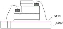
实施例1Example 1
参看图1,在本发明的第一个实施例中,提供一种发光二极管,由半导体外延材料制作的用于发光的半导体层序列1100,半导体层序列包括第一半导体层、第二半导体层和位于两者之间的发光层;第一电连接层,与第一半导体层电连接,第二电连接层,与第二半导体层电连接,第一电连接层和第二电连接层可以为金属或者透明导电材料;在半导体层序列1100的出光方向上设置有反射式偏振层1200,通过预设方向光而反射其他方向的出光,预设方向光例如垂直于反射式偏振层1200的光,反射式偏振层1200让发光二极管输出线偏振光。Referring to FIG. 1, in a first embodiment of the present invention, a light emitting diode is provided, a
半导体层序列1100和反射式偏振层1200之间可以设有中间层1300,中间层1300例如作为钝化层保护发光二极管的透明绝缘层、作为扩展电流的透明导电层或者波长转换层,半导体层序列1100或者发光层远离反射式偏振层1200的一侧设置有漫反射部1400,漫反射部1400用于将光散射成多个方向并形成反射,漫反射部1400例如由具有非平整表面的金属组成,例如金、铜、钛、铝、铂、钌、铑或者银,非平整表面例如具有非周期的不规则图形、粗化面。An
在本实施例中,反射式偏振层1200仅透过垂直于其表面的出光,而反射其他方向的光,E1光由半导体层序列1100激发出光,非垂直于反射式偏振层1200的角度入射,形成被反射式偏振层1200反射的光E2,E2被漫反射部1400漫反射形成光E3、E4和E5,其中E3的方向为垂直于反射式偏振层1200的角度,则可透过反射式偏振层1200,E3、E4按上述方式继续进行循环萃取,直至最终形成线出光。反射式偏振层1200单独的有益效果。In this embodiment, the reflective
发光二极管包括支撑半导体层序列1100的衬底1500,衬底1500材料例如为铜、金、蓝宝石、砷化镓、硅、陶瓷、玻璃或者碳化硅等。The light emitting diode includes a
实施例2Example 2
参看图2,在本发明的第二个实施例中,提供一种发光二极管,由半导体外延材料制作的用于发光的半导体层序列2100,半导体层序列2100包括第一半导体层、第二半导体层和位于两者之间的发光层;第一电连接层,与第一半导体层电连接,第二电连接层,与第二半导体层电连接,第一电连接层和第二电连接层可以为金属或者透明导电材料;在半导体层序列2100的出光方向上设置有反射式偏振层2200,通过预设方向光而反射其他方向的出光,预设方向光例如垂直于反射式偏振层2200的光,反射式偏振层2200让发光二极管输出线偏振光。Referring to FIG. 2, in a second embodiment of the present invention, a light emitting diode is provided, a
半导体层序列2100和反射式偏振层2200之间可以设有中间层2300,中间层2300例如透明绝缘层、透明导电层或者波长转换层。半导体层序列2100或者发光层远离反射式偏振层2200的一侧设置有漫反射部2400,漫反射部2400例如由具有非平整表面的金属组成,非平整表面例如具有非周期的不规则图形、粗化面。漫反射部2400的有益效果散射并反射光。An
发光二极管包括支撑半导体层序列2100的衬底2500,衬底2500位于半导体层序列2100和漫反射部2400之间,衬底2500的材料例如为玻璃或者蓝宝石等透明材料。The light emitting diode includes a
实施例3Example 3
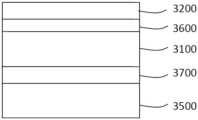
参看图3,在本发明的第三个实施例中,提供一种发光二极管,由半导体外延材料制作的用于发光的半导体层序列3100,半导体层序列3100包括第一半导体层、第二半导体层和位于两者之间的发光层;第一电连接层,与第一半导体层电连接,第二电连接层,与第二半导体层电连接,第一电连接层和第二电连接层可以为金属或者透明导电材料;在半导体层序列3100的出光方向上设置有反射式偏振层3200,通过预设方向光而反射其他方向的出光,预设方向光例如垂直于反射式偏振层3200的光,反射式偏振层3200让发光二极管输出线偏振光。Referring to FIG. 3, in a third embodiment of the present invention, a light emitting diode is provided, a
半导体层序列3100和反射式偏振层3200之间可以设有中间层,中间层例如透明绝缘层、透明导电层或者波长转换层。发光二极管在半导体层序列3100或者发光层与反射式偏振层3200之间设置有非平整层3600,例如由具有非平整表面的透明绝缘材料或者透明导电材料组成,非平整层可以作为中间层,非平整表面3600例如具有非周期的不规则图形、粗化面。非平整表面3600的有益效果。An intermediate layer may be provided between the
发光二极管在半导体层序列3100或者发光层远离反射式偏振层3200的一侧设置有镜面反射层3700,例如反射金属、分散式布拉格反射DBR或者全角反射镜ODR结构,一些实施情况下,镜面反射层3700设置在半导体层序列3100和衬底3500之间。The light emitting diode is provided with a
发光二极管包括支撑半导体层序列3100的衬底3500,衬底3500材料例如为铜、金、蓝宝石、砷化镓、硅、陶瓷、玻璃或者碳化硅等。The light emitting diode includes a
实施例4Example 4
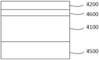
参看图4,在本发明的第四个实施例中,提供一种发光二极管,由半导体外延材料制作的用于发光的半导体层序列4100,半导体层序列4100包括第一半导体层、第二半导体层和位于两者之间的发光层;第一电连接层,与第一半导体层电连接,第二电连接层,与第二半导体层电连接,第一电连接层和第二电连接层可以为金属或者透明导电材料;在半导体层序列4100的出光方向上设置有反射式偏振层4200,通过预设方向光而反射其他方向的出光,预设方向光例如垂直于反射式偏振层4200的光,反射式偏振层4200让发光二极管输出线偏振光。Referring to FIG. 4 , in a fourth embodiment of the present invention, a light emitting diode is provided, a
半导体层序列4100和反射式偏振层4200之间可以设有中间层,中间层例如透明绝缘层、透明导电层或者波长转换层。发光二极管在半导体层序列4100或者发光层与反射式偏振层4200之间设置有非平整层4600,例如由具有非平整表面的透明绝缘材料或者透明导电材料组成,在一些实施情况中,非平整层4600作为中间层,在中间层做非平整表面,非平整表面例如具有非周期的不规则图形、粗化面。An intermediate layer may be provided between the
发光二极管包括支撑半导体层序列4100的反射性衬底4500,衬底4500材料例如反射金属或者陶瓷基板。The light-emitting diode comprises a
实施例5Example 5
参看图5,在本发明的第五个实施例中,提供一种发光二极管,由半导体外延材料制作的用于发光的半导体层序列5100,半导体层序列5100包括第一半导体层、第二半导体层和位于两者之间的发光层;第一电连接层,与第一半导体层电连接,第二电连接层,与第二半导体层电连接,第一电连接层和第二电连接层可以为金属或者透明导电材料;在半导体层序列5100的出光方向上设置有反射式偏振层5200,通过预设方向光而反射其他方向的出光,预设方向光例如垂直于反射式偏振层5200的光,反射式偏振层5200让发光二极管输出线偏振光。Referring to FIG. 5 , in a fifth embodiment of the present invention, a light emitting diode is provided, a
半导体层序列5100和反射式偏振层5200之间可以设有中间层,中间层例如透明绝缘层、透明导电层或者波长转换层。发光二极管在半导体层序列5100或者发光层与反射式偏振层5200之间设置有非平整层5600,例如由具有非平整表面的透明绝缘材料或者透明导电材料组成,在一些实施情况中,非平整层5600作为中间层,在中间层做非平整表面,非平整表面例如具有非周期的不规则图形、粗化面。Between the
发光二极管包括支撑半导体层序列的透明衬底5500,衬底5500材料例如为玻璃或者蓝宝石等透明材料。发光二极管在衬底5500远离半导体层序列的一侧设置有镜面反射层5400,镜面反射层5400材料包括:反射金属、分散式布拉格反射DBR、全角反射镜ODR结构或者以上的结合。The light emitting diode includes a
实施例6Example 6
参看图6,在本发明的第六个实施例中,提供一种发光二极管,由半导体外延材料制作的用于发光的半导体层序列6100,半导体层序列6100包括第一半导体层、第二半导体层和位于两者之间的发光层;第一电连接层,与第一半导体层电连接,第二电连接层,与第二半导体层电连接,第一电连接层和第二电连接层可以为金属或者透明导电材料;在半导体层序列6100的出光方向上设置有反射式偏振层6200,通过预设方向光而反射其他方向的出光,预设方向光例如垂直于反射式偏振层6200的光,反射式偏振层6200让发光二极管输出线偏振光。Referring to FIG. 6 , in the sixth embodiment of the present invention, a light emitting diode is provided, a
半导体层序列6100和反射式偏振层6200之间可以设有中间层6300,中间层6300例如透明绝缘层、透明导电层或者波长转换层。在本实施例中,半导体层序列6100靠近反射式偏振层6200一侧设置有非平整表面,非平整表面例如具有非周期的不规则图形、粗化面。An
发光二极管包括支撑半导体层序列6100的透明衬底6500,衬底6500材料例如为玻璃或者蓝宝石等透明材料。发光二极管在衬底6500远离半导体层序列6100的一侧设置有镜面反射层6400,镜面反射层6400材料包括:反射金属、分散式布拉格反射DBR、全角反射镜ODR结构或者以上的结合。The light emitting diode includes a
实施例7Example 7
参看图7,在本发明的第七个实施例中,提供一种发光二极管,由半导体外延材料制作的用于发光的半导体层序列7100,半导体层序列7100包括第一半导体层、第二半导体层和位于两者之间的发光层;第一电连接层,与第一半导体层电连接,第二电连接层,与第二半导体层电连接,第一电连接层和第二电连接层可以为金属或者透明导电材料;在半导体层序列的出光方向上设置有反射式偏振层7200,通过预设方向光而反射其他方向的出光,预设方向光例如垂直于反射式偏振层7200的光,反射式偏振层7200让发光二极管输出线偏振光。Referring to FIG. 7 , in a seventh embodiment of the present invention, a light emitting diode is provided, a
半导体层序列7100和反射式偏振层7200之间可以设有中间层7300,中间层7300例如透明绝缘层、透明导电层或者波长转换层。在本实施例中,半导体层序列7100靠近反射式偏振层7200一侧设置有非平整表面,非平整表面例如具有非周期的不规则图形、粗化面,在本实施例中,优选的,采用表面粗化结构。An
发光二极管包括支撑半导体层序列7100的衬底7500,衬底7500材料例如为玻璃或者蓝宝石等透明材料。半导体层序列7100和发光二极管在衬底7500之间设置有镜面反射层7400,镜面反射层7400材料包括:反射金属、分散式布拉格反射DBR、全角反射镜ODR结构或者以上的结合。The light emitting diode includes a
参看图8,图例是粗化表面发光二极管的示意图,其包括n型电极8710,由n 型层8110、p型层8120、发光层8130组成的半导体层序列8100、p型电极8720,该p型电极8720已通过键合层8800倒装粘合到硅衬底8500,该硅衬底可视为包括p型电极。所述n型层8110、p型层8120和位于二者之间的发光层8130由 (Al,Ga,In)N合金制成。采用干法或者湿法蚀刻方法来粗化n型层8110的表面。为了能获得所需表面,有必要设定合适的条件,例如对于干式蚀刻来说设定合适的等离子体化学成分和等离子体功率,和对于湿法蚀刻来说设定合适的蚀刻溶液和温度。在氮化镓基的实施例中,应该沿着它的c轴生长而且这种n型GaN表面应该是N面,原因在于在N面上观察各向异性蚀刻要比在Ga面上容易得多。8, the legend is a schematic diagram of a roughened surface light emitting diode, which includes an n-
注意c平面GaN具有如下结构:只包括Ga原子的平面和只包括N原子的平面是堆在一起的,或者是交替地叠起来的。如果一个表面是Ga面,则相对的表面是N面。从晶体生长和器件性能的观点看,Ga面c平面GaN一般是优选的,基于这个事实,N面GaN可借助激光剥离LLO技术来制备,或者可以选择地,LED结构可以在c平面大块GaN晶片上生长。Note that c-plane GaN has a structure in which a plane including only Ga atoms and a plane including only N atoms are stacked together, or alternately stacked. If one face is a Ga face, the opposite face is an N face. From a crystal growth and device performance standpoint, Ga-plane c-plane GaN is generally preferred, based on the fact that N-plane GaN can be fabricated by means of laser lift-off LLO techniques, or alternatively, LED structures can be fabricated on c-plane bulk GaN grown on the wafer.
光从活性区发光层射出,射向粗化的n型GaN表面并被该表面散射,该表面并不将所述光反射回所述活性区有源区。所希望的是,所述p侧和偏振层具有高反射性以减少光吸收,例如采用p侧镜面反射层8400或者p侧反射电极设计,并从而使朝向所述n型GaN表面反射的光增多。在实验结果中,已经确定的是:对比带有平坦表面的发光二极管,本发明采用的带有粗化表面的发光二极管的上向光(upward light)输出功率明显增大。Light exits the active region light-emitting layer, strikes and is scattered by the roughened n-type GaN surface, which does not reflect the light back to the active region active region. Desirably, the p-side and polarizing layers are highly reflective to reduce light absorption, such as with a p-side specular
在半导体层序列8100和反射式偏振层8200之间选择性可设置中间层8300,此处中间层8300并非是必须的,中间层8300例如透明绝缘层、透明导电层或者波长转换层,通过反射式偏振层8200结合粗化表面的散射,让光源最大限度输出线偏振光,避免光通浪费。An
参看图9,图例是一款可适用大电流的垂直产品结构示意图,提供一种发光二极管,由半导体外延材料制作的用于发光的半导体层序列9100,半导体层序列9100包括第一半导体层(n型层9110)、第二半导体层(p型层9120)和位于两者之间的发光层9130;通过第一电连接层9711,将n型电极9710与第一半导体层电连接,即第一电连接层9711通过绝缘层9900构成的导电通道与n型层9110电连接,在一些情况下绝缘层9900可以包括DBR;第二电连接层9721,与第二半导体层电连接,第一电连接层9810和第二电连接层9820通过绝缘层9900电隔离,发光二极管通过第二电连接层9721引出p型电极9720,第二电连接层9721可以包括反射金属,第一电连接层9711和第二电连接层9721包括金属或者透明导电材料。Referring to FIG. 9, the legend is a schematic diagram of a vertical product structure suitable for high current, providing a light emitting diode, a
导电衬底9500通过键合层9800与第一电连接层9711粘合,n型电极9710设置在导电衬底9500远离键合层9800的一侧。The
在本实施例中,半导体层序列的厚度优选为5μm至10μm的薄膜结构,或者也可以为10μm至20μm,发光二极管芯片的出光角小于或等于120°。In this embodiment, the thickness of the semiconductor layer sequence is preferably a thin film structure of 5 μm to 10 μm, or can also be 10 μm to 20 μm, and the light emitting angle of the light emitting diode chip is less than or equal to 120°.
在半导体层序列9100的出光方向上设置有反射式偏振层9200,通过预设方向光而反射其他方向的出光,预设方向光例如垂直于反射式偏振层9200的光,反射式偏振层9200让发光二极管输出线偏振光。半导体层序列9100和反射式偏振层9200之间可以设有中间层9300,中间层9300例如透明绝缘层、透明导电层或者波长转换层。A reflective
在本实施例中,半导体层序列9100靠近反射式偏振层9200一侧设置有非平整表面,非平整表面例如具有非周期的不规则图形、粗化面,在本实施例中,优选的,采用表面粗化结构。In this embodiment, the
实施例8Example 8
参看图10,在本发明的第八个实施例中,提供一种发光二极管,由半导体外延材料制作的用于发光的半导体层序列10100,半导体层序列10100包括第一半导体层n型层、第二半导体层p型层和位于两者之间的发光层;第一电连接层,与第一半导体层电连接,第二电连接层,与第二半导体层电连接,第一电连接层和第二电连接层可以为金属或者透明导电材料;在半导体层序列10100的出光方向上设置有反射式偏振层10200,通过预设方向光而反射其他方向的出光,预设方向光例如垂直于反射式偏振层10200的光,反射式偏振层10200让发光二极管输出线偏振光。Referring to FIG. 10 , in the eighth embodiment of the present invention, a light emitting diode is provided, a
半导体层序列10100和反射式偏振层10200之间可以设有中间层10300,中间层10300例如透明绝缘层、透明导电层或者波长转换层。在本实施例中,半导体层序列10100靠近反射式偏振层10200一侧设置有非平整表面,非平整表面例如具有非周期的不规则图形、粗化面。An
发光二极管包括支撑半导体层序列10100的反射衬底10500,衬底10500材料例如为反射金属。The light-emitting diode comprises a
实施例9Example 9
参看图11,在本发明的第九个实施例中,提供一种发光二极管,由半导体外延材料制作的用于发光的半导体层序列11100,半导体层序列11100包括第一半导体层、第二半导体层和位于两者之间的发光层;第一电连接层,与第一半导体层电连接,第二电连接层,与第二半导体层电连接,第一电连接层和第二电连接层可以为金属或者透明导电材料;在半导体层序列11100的出光方向上设置有反射式偏振层11200,通过预设方向光而反射其他方向的出光,预设方向光例如垂直于反射式偏振层11200的光,反射式偏振层11200让发光二极管输出线偏振光。Referring to FIG. 11, in the ninth embodiment of the present invention, a light emitting diode is provided, a
半导体层序列11100和反射式偏振层11200之间可以设有中间层11300,中间层11300例如透明绝缘层、透明导电层或者波长转换层。在本实施例中,半导体层序列11100靠近反射式偏振层11200一侧设置有非平整表面,非平整表面例如具有非周期的不规则图形、粗化面。An
发光二极管包括支撑半导体层序列11100的透明衬底11500,衬底11500材料例如为玻璃或者蓝宝石等透明材料。发光二极管在衬底11500远离半导体层序列11100的一侧设置有镜面反射层11400,镜面反射层11400材料包括:反射金属、分散式布拉格反射DBR、全角反射镜ODR结构或者以上的结合。The light emitting diode includes a
实施例10Example 10
参看图12,在本发明的第十个实施例中,提供一种发光二极管,由半导体外延材料制作的用于发光的半导体层序列11100,半导体层序列11100包括第一半导体层、第二半导体层和位于两者之间的发光层;第一电连接层,与第一半导体层电连接,第二电连接层,与第二半导体层电连接,第一电连接层和第二电连接层可以为金属或者透明导电材料;在半导体层序列11100的出光方向上设置有反射式偏振层11200,通过预设方向光而反射其他方向的出光,预设方向光例如垂直于反射式偏振层11200的光,反射式偏振层11200让发光二极管输出线偏振光。Referring to FIG. 12 , in the tenth embodiment of the present invention, a light emitting diode is provided, and a
半导体层序列11100和反射式偏振层11200之间可以设有中间层11300,中间层11300例如透明绝缘层、透明导电层或者波长转换层。An
发光二极管包括支撑半导体层序列11100的透明衬底11500,衬底11500材料例如为玻璃或者蓝宝石等透明材料。发光二极管在衬底11500远离半导体层序列11100的一侧设置有镜面反射层11400,镜面反射层11400材料包括:反射金属、分散式布拉格反射DBR、全角反射镜ODR结构或者以上的结合。The light emitting diode includes a
在本实施例中,半导体层序列11100与透明衬底11500之间设置有非平整表面,非平整表面例如具有非周期的不规则图形、粗化面。In this embodiment, an uneven surface is disposed between the
实施例11Example 11
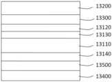
参看图13,在本发明的第十一个实施例中,提供一种发光二极管,由半导体外延材料制作的用于发光的半导体层序列13100,半导体层序列包括第一半导体层(n型层13110)、第二半导体层(p型层13120)和位于两者之间的发光层13130;第一电连接层,与第一半导体层电连接,第二电连接层,与第二半导体层电连接,第一电连接层和第二电连接层可以为金属或者透明导电材料;在半导体层序列13100的出光方向上设置有反射式偏振层13200,通过预设方向光而反射其他方向的出光,预设方向光例如垂直于反射式偏振层13200的光,反射式偏振层13200让发光二极管输出线偏振光。Referring to FIG. 13 , in the eleventh embodiment of the present invention, a light emitting diode is provided, a semiconductor layer sequence 13100 made of semiconductor epitaxial material for light emission, and the semiconductor layer sequence includes a first semiconductor layer (n-type layer 13110 ). ), the second semiconductor layer (p-type layer 13120), and the light-emitting
反射式偏振层13200和半导体层序列13100之间可以设有中间层13300,中间层13300例如透明绝缘层、透明导电层或者波长转换层。An
发光二极管包括支撑半导体层序列13100的透明衬底13500,衬底13500材料例如为玻璃或者蓝宝石等透明材料。发光二极管在衬底13500远离或者靠近半导体层序列13100的一侧设置有镜面反射层13400,镜面反射层13400材料包括:反射金属、分散式布拉格反射DBR、全角反射镜ODR结构或者以上的结合。The light emitting diode includes a
在本实施例中,半导体层序列内设置有非平整表面,非平整表面例如具有非周期的不规则图形、粗化面,例如包括但不限于在第一半导体层和透明衬底之间设置有不规则图案的GaN半导体层作为非平整层13140,或者在第一半导体层或者发光层增加坑状结构的非平整表面。In this embodiment, the semiconductor layer sequence is provided with a non-planar surface, for example, the non-planar surface has non-periodic irregular patterns and roughened surfaces, for example, including but not limited to, a non-planar surface is provided between the first semiconductor layer and the transparent substrate. The irregular pattern of the GaN semiconductor layer is used as the
实施例12Example 12
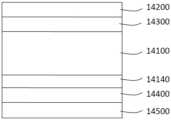
参看图14,在本发明的第十二个实施例中,提供一种发光二极管,由半导体外延材料制作的用于发光的半导体层序列14100,半导体层序列14100包括第一半导体层、第二半导体层和位于两者之间的发光层;第一电连接层,与第一半导体层电连接,第二电连接层,与第二半导体层电连接,第一电连接层和第二电连接层可以为金属或者透明导电材料;在半导体层序列14100的出光方向上设置有反射式偏振层14200,通过预设方向光而反射其他方向的出光,预设方向光例如垂直于反射式偏振层14200的光,反射式偏振层14200让发光二极管输出线偏振光。Referring to FIG. 14, in the twelfth embodiment of the present invention, a light emitting diode is provided, a
半导体层序列14100和反射式偏振层14200之间可以设有中间层14300,中间层14300例如透明绝缘层、透明导电层或者波长转换层。An
发光二极管包括支撑半导体层序列14100的衬底14500,衬底14500材料例如铜、金、蓝宝石、砷化镓、硅、陶瓷、玻璃或者碳化硅等。半导体层序列14100与发光二极管在衬底14500之间设置有靠近半导体层序列14100的非平整层14140和靠近衬底14500的镜面反射层14400,镜面反射层,镜面反射层14400材料包括:反射金属、分散式布拉格反射DBR、全角反射镜ODR结构或者以上的结合,其中非平整层14140例如具有非周期的不规则图形、粗化面,非平整层也可以由颗粒构成,例如氮化铝、氧化铝颗粒或者氧化硅颗粒。The light emitting diode comprises a
实施例13Example 13
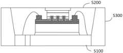
参看图15,在本发明的第十三个实施例中,提供了一种发光装置,发光装置具有支架S100,具有用于安装发光二极管芯片的安装表面S110,发光二极管芯片采用了第一个实施例至第十二实施例所提供的发光芯粒。15, in a thirteenth embodiment of the present invention, a light-emitting device is provided, the light-emitting device has a bracket S100, and has a mounting surface S110 for mounting a light-emitting diode chip, the light-emitting diode chip adopts the first implementation The light-emitting core particles provided in the twelfth embodiment.
参看图16,发光二极管芯片在一些实施方式,封装材料层S200至少设置在发光二极管出光面,封装材料层S200包括透明胶或者反射胶、黑胶、其他不透光胶或者组合,但该封装材料层S200不构成必要的条件。16 , in some embodiments of the light-emitting diode chip, the packaging material layer S200 is disposed at least on the light-emitting surface of the light-emitting diode, and the packaging material layer S200 includes transparent glue or reflective glue, black glue, other opaque glue or a combination, but the packaging material Layer S200 does not constitute a necessary condition.
参看图17,在一些实施例中,通过封装材料层S200将发光二极管芯粒密封在碗杯S300中。Referring to FIG. 17 , in some embodiments, the light-emitting diode die is sealed in the bowl S300 through the packaging material layer S200.
实施例14Example 14
参看图18,在本发明的第十四个实施例中,提供了包括衬底18500面出光的发光二极管芯片的发光装置,发光装置具有支架S100,具有用于安装发光二极管芯片的安装表面S110,发光二极管通过第一电连接层(例如:n型电极18710)和第二电连接层(例如:p型电极18720)与安装表面S110连接,发光二极管包括支撑半导体层序列18100的透明衬底18500,衬底18500材料例如为玻璃或者蓝宝石等透明材料,衬底18500材料可以减薄或者移除,在本实施例中,半导体层序列18100厚度可以为10μm至500μm。18, in a fourteenth embodiment of the present invention, a light-emitting device including a light-emitting diode chip that emits light from a
在反射式偏振层18200与衬底18500之间可以设有中间层18300,中间层18300例如透明绝缘层、透明导电层或者波长转换层。An
衬底18500靠近半导体层序列18100的一侧为非平整面,设有由湿法或者干法制得的图案图形,半导体层序列18100通过图案衬底长晶降低外延缺陷,提升长晶质量。The side of the
在一些实施方式中,可通过封装材料层S200密封发光二极管,封装材料层S200可是透明胶或者反射胶、黑胶或者其他不透光胶。In some embodiments, the light emitting diode may be sealed by the packaging material layer S200, which may be transparent glue or reflective glue, black glue or other opaque glue.
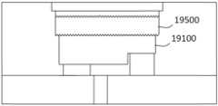
参看图19,在本实施例的基础上,于衬底19500远离半导体层序列19100的一侧,即光的衬底19500出射面,用以增强光萃取制作粗化结构,同时实现增强出光的散射的作用。粗化结构可不等同于衬底图案。Referring to FIG. 19 , on the basis of this embodiment, the side of the
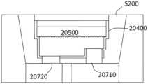
参看图20,关于本实施例的镜面反射层20400设计,在一些设计中,采用钝化反射层包覆发光二极管底侧和/或侧部,例如采用DBR反射叠层,或者结合反射性n型电极20710和/或p型电极20720材料增加向衬底20500出光面的光反射。在一些设计中,利用白胶作为封装材料层S200至少部分覆盖发光二极管底侧和/或侧部,形成镜面反射。Referring to Figure 20, regarding the specular
实施例15Example 15
参看图21,提供一种发光装置,包括,发光装置具有支架S100,具有用于安装发光二极管芯片的安装表面S110,其中发光二极管,由半导体外延材料制作的用于发光的半导体层序列21100,半导体层序列21100包括第一半导体层、第二半导体层和位于两者之间的发光层;第一电连接层,与第一半导体层电连接,第二电连接层,与第二半导体层电连接,第一电连接层和第二电连接层通过焊线与安装表面S110电连接,在半导体层序列21100的出光方向上设置有反射式偏振层21200,通过预设方向光而反射其他方向的出光,预设方向光例如垂直于反射式偏振层21200的光,反射式偏振层21200让发光二极管输出线偏振光。21, a light-emitting device is provided, comprising, the light-emitting device has a support S100, has a mounting surface S110 for mounting a light-emitting diode chip, wherein the light-emitting diode, a
在反射式偏振层21200与衬底21500之间可以选择性设有中间层,中间层例如透明绝缘层、透明导电层或者波长转换层。Between the reflective
参看图22,发光二极管包括支撑半导体层序列22100的衬底22500,衬底22500材料例如为玻璃或者蓝宝石等透明材料。发光二极管通过反射粘合层S400粘附在安装表面上,反射粘合层S400例如金属或者反射胶。在一些设计中,通过具有反射性的封装材料将发光二极管固定在发光装置中。在一些设计中,发光装置设计环绕发光二极管的白墙S500,白墙S500可同时设置在安装表面的间隙中。22, the light emitting diode includes a
实施例16Example 16
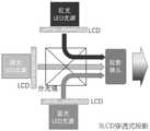
参看图23和图24,提供一种投影仪,包括投影仪壳体,电源,发光部分,采用上述实施例中任意一种发光二极管或者发光装置,投影仪包括红、绿、蓝三色LED光源,不同光源分别对应LCD液晶板,简单来说,通过图中的光路设计,经过分光镜汇聚到投影镜头形成出光。投影仪比现有技术的产品具有更好的光电效率,给予用户更佳的光感体验。23 and 24, a projector is provided, including a projector housing, a power supply, and a light-emitting part, using any one of the light-emitting diodes or light-emitting devices in the above-mentioned embodiments, and the projector includes three-color LED light sources of red, green, and blue. , Different light sources correspond to the LCD liquid crystal panel respectively. In simple terms, through the light path design in the figure, the light is gathered to the projection lens through the beam splitter to form light. The projector has better photoelectric efficiency than products in the prior art, giving users a better light perception experience.
以上所述仅是本发明的优选实施方式,应当指出,对于本技术领域的普通技术人员来说,在不脱离本发明技术原理的前提下,还可以做出若干改进和替换,这些改进和替换也应视为本发明的保护范围。The above are only the preferred embodiments of the present invention. It should be pointed out that for those skilled in the art, without departing from the technical principle of the present invention, several improvements and replacements can be made. These improvements and replacements It should also be regarded as the protection scope of the present invention.
Claims (35)
Translated fromChinesePriority Applications (2)
| Application Number | Priority Date | Filing Date | Title |
|---|---|---|---|
| CN202010631519.5ACN111987202A (en) | 2020-07-03 | 2020-07-03 | Light-emitting diode, light-emitting device and projector thereof |
| US17/365,347US12032276B2 (en) | 2020-07-03 | 2021-07-01 | Light emitting diode, light emitting device and projector device |
Applications Claiming Priority (1)
| Application Number | Priority Date | Filing Date | Title |
|---|---|---|---|
| CN202010631519.5ACN111987202A (en) | 2020-07-03 | 2020-07-03 | Light-emitting diode, light-emitting device and projector thereof |
Publications (1)
| Publication Number | Publication Date |
|---|---|
| CN111987202Atrue CN111987202A (en) | 2020-11-24 |
Family
ID=73438965
Family Applications (1)
| Application Number | Title | Priority Date | Filing Date |
|---|---|---|---|
| CN202010631519.5APendingCN111987202A (en) | 2020-07-03 | 2020-07-03 | Light-emitting diode, light-emitting device and projector thereof |
Country Status (2)
| Country | Link |
|---|---|
| US (1) | US12032276B2 (en) |
| CN (1) | CN111987202A (en) |
Cited By (4)
| Publication number | Priority date | Publication date | Assignee | Title |
|---|---|---|---|---|
| CN113270526A (en)* | 2021-01-05 | 2021-08-17 | 朗明纳斯光电(厦门)有限公司 | Light emitting diode, light emitting device and projector thereof |
| CN113314650A (en)* | 2021-04-06 | 2021-08-27 | 华灿光电(苏州)有限公司 | Light emitting diode chip for improving lateral light emitting intensity and manufacturing method thereof |
| CN113874768A (en)* | 2021-07-16 | 2021-12-31 | 福建晶安光电有限公司 | Polarizing element, light emitting diode, and light emitting device |
| WO2025166764A1 (en)* | 2024-02-08 | 2025-08-14 | 京东方科技集团股份有限公司 | Light-emitting substrate and preparation method therefor, display substrate, and display apparatus |
Citations (6)
| Publication number | Priority date | Publication date | Assignee | Title |
|---|---|---|---|---|
| CN101088175A (en)* | 2004-10-29 | 2007-12-12 | 3M创新有限公司 | Polarized LED |
| CN101806401A (en)* | 2009-02-17 | 2010-08-18 | 富士迈半导体精密工业(上海)有限公司 | Light emitting diode light source |
| US20100271566A1 (en)* | 2009-04-27 | 2010-10-28 | Chimei Innolux Corporation | Light emitting diode, backlight module and liquid crystal display apparatus |
| US9291758B2 (en)* | 2011-06-17 | 2016-03-22 | University Of Florida Research Foundation, Inc. | Laterally aligned colloidal nanorods assemblies |
| CN107544180A (en)* | 2017-09-26 | 2018-01-05 | 京东方科技集团股份有限公司 | Light emitting diode, backlight module and liquid crystal display device |
| CN210607312U (en)* | 2019-09-19 | 2020-05-22 | 朗明纳斯光电(厦门)有限公司 | led |
Family Cites Families (1)
| Publication number | Priority date | Publication date | Assignee | Title |
|---|---|---|---|---|
| US20070284567A1 (en)* | 2004-09-10 | 2007-12-13 | Luminus Devices, Inc | Polarization recycling devices and methods |
- 2020
- 2020-07-03CNCN202010631519.5Apatent/CN111987202A/enactivePending
- 2021
- 2021-07-01USUS17/365,347patent/US12032276B2/enactiveActive
Patent Citations (6)
| Publication number | Priority date | Publication date | Assignee | Title |
|---|---|---|---|---|
| CN101088175A (en)* | 2004-10-29 | 2007-12-12 | 3M创新有限公司 | Polarized LED |
| CN101806401A (en)* | 2009-02-17 | 2010-08-18 | 富士迈半导体精密工业(上海)有限公司 | Light emitting diode light source |
| US20100271566A1 (en)* | 2009-04-27 | 2010-10-28 | Chimei Innolux Corporation | Light emitting diode, backlight module and liquid crystal display apparatus |
| US9291758B2 (en)* | 2011-06-17 | 2016-03-22 | University Of Florida Research Foundation, Inc. | Laterally aligned colloidal nanorods assemblies |
| CN107544180A (en)* | 2017-09-26 | 2018-01-05 | 京东方科技集团股份有限公司 | Light emitting diode, backlight module and liquid crystal display device |
| CN210607312U (en)* | 2019-09-19 | 2020-05-22 | 朗明纳斯光电(厦门)有限公司 | led |
Cited By (7)
| Publication number | Priority date | Publication date | Assignee | Title |
|---|---|---|---|---|
| CN113270526A (en)* | 2021-01-05 | 2021-08-17 | 朗明纳斯光电(厦门)有限公司 | Light emitting diode, light emitting device and projector thereof |
| CN113314650A (en)* | 2021-04-06 | 2021-08-27 | 华灿光电(苏州)有限公司 | Light emitting diode chip for improving lateral light emitting intensity and manufacturing method thereof |
| CN113314650B (en)* | 2021-04-06 | 2022-05-13 | 华灿光电(苏州)有限公司 | Light emitting diode chip capable of improving lateral light-emitting intensity and manufacturing method thereof |
| CN113874768A (en)* | 2021-07-16 | 2021-12-31 | 福建晶安光电有限公司 | Polarizing element, light emitting diode, and light emitting device |
| WO2023283913A1 (en)* | 2021-07-16 | 2023-01-19 | 福建晶安光电有限公司 | Polarization element, light-emitting diode and light-emitting apparatus |
| CN113874768B (en)* | 2021-07-16 | 2024-09-17 | 福建晶安光电有限公司 | Polarization element, light emitting diode and light emitting device |
| WO2025166764A1 (en)* | 2024-02-08 | 2025-08-14 | 京东方科技集团股份有限公司 | Light-emitting substrate and preparation method therefor, display substrate, and display apparatus |
Also Published As
| Publication number | Publication date |
|---|---|
| US20220004089A1 (en) | 2022-01-06 |
| US12032276B2 (en) | 2024-07-09 |
Similar Documents
| Publication | Publication Date | Title |
|---|---|---|
| US20250294937A1 (en) | Light emitting diode | |
| US12002902B2 (en) | Light emitting device, and method for manufacturing thereof | |
| CN111987202A (en) | Light-emitting diode, light-emitting device and projector thereof | |
| JP5591487B2 (en) | LIGHT EMITTING DEVICE, PACKAGE AND SYSTEM INCLUDING THE SAME, AND MANUFACTURING METHOD THEREOF | |
| KR101898680B1 (en) | Nano-structured light emitting device | |
| JP4447806B2 (en) | Light emitting device | |
| CN102800781B (en) | Semiconductor light emitting device and method of manufacturing the same | |
| JP5620359B2 (en) | Reflective mounting substrate for light emitting diodes | |
| JP5719110B2 (en) | Light emitting element | |
| TWI641162B (en) | Light-emitting diode and light-emitting device | |
| CN104885235B (en) | For the LED of the growth substrates with forming of side transmitting | |
| JPH08102549A (en) | Semiconductor light emitting element | |
| CN111509100A (en) | led | |
| JP2002319705A (en) | LED device | |
| JP6320769B2 (en) | Light emitting element | |
| CN105390586A (en) | Light emitting device package | |
| KR20120134338A (en) | A light emitting device | |
| JP2012244158A (en) | Light emitting device, light emitting device package, and light unit | |
| JP2016152413A (en) | Light-emitting element package and lighting system including the same | |
| KR20130025232A (en) | A light emitting device | |
| JP6385680B2 (en) | Light emitting element | |
| CN117038817A (en) | Light emitting diode and light emitting device | |
| TWI539619B (en) | Light-emitting diode structure, lamp device and method for forming light-emitting diode structure | |
| JP2014150256A (en) | Light emitting element | |
| TWM511125U (en) | Light-emitting diode chip and light-emitting device |
Legal Events
| Date | Code | Title | Description |
|---|---|---|---|
| PB01 | Publication | ||
| PB01 | Publication | ||
| SE01 | Entry into force of request for substantive examination | ||
| SE01 | Entry into force of request for substantive examination | ||
| RJ01 | Rejection of invention patent application after publication | ||
| RJ01 | Rejection of invention patent application after publication | Application publication date:20201124 |