CN111971853B - Loop antenna, loop antenna unit and electronic equipment - Google Patents
Loop antenna, loop antenna unit and electronic equipmentDownload PDFInfo
- Publication number
- CN111971853B CN111971853BCN201880091196.6ACN201880091196ACN111971853BCN 111971853 BCN111971853 BCN 111971853BCN 201880091196 ACN201880091196 ACN 201880091196ACN 111971853 BCN111971853 BCN 111971853B
- Authority
- CN
- China
- Prior art keywords
- ring
- antenna unit
- loop
- substrate
- layer
- Prior art date
- Legal status (The legal status is an assumption and is not a legal conclusion. Google has not performed a legal analysis and makes no representation as to the accuracy of the status listed.)
- Active
Links
Images


Classifications
- H—ELECTRICITY
- H01—ELECTRIC ELEMENTS
- H01Q—ANTENNAS, i.e. RADIO AERIALS
- H01Q7/00—Loop antennas with a substantially uniform current distribution around the loop and having a directional radiation pattern in a plane perpendicular to the plane of the loop
- G—PHYSICS
- G06—COMPUTING OR CALCULATING; COUNTING
- G06K—GRAPHICAL DATA READING; PRESENTATION OF DATA; RECORD CARRIERS; HANDLING RECORD CARRIERS
- G06K19/00—Record carriers for use with machines and with at least a part designed to carry digital markings
- G06K19/06—Record carriers for use with machines and with at least a part designed to carry digital markings characterised by the kind of the digital marking, e.g. shape, nature, code
- G06K19/067—Record carriers with conductive marks, printed circuits or semiconductor circuit elements, e.g. credit or identity cards also with resonating or responding marks without active components
- G06K19/07—Record carriers with conductive marks, printed circuits or semiconductor circuit elements, e.g. credit or identity cards also with resonating or responding marks without active components with integrated circuit chips
- G06K19/077—Constructional details, e.g. mounting of circuits in the carrier
- H—ELECTRICITY
- H01—ELECTRIC ELEMENTS
- H01Q—ANTENNAS, i.e. RADIO AERIALS
- H01Q1/00—Details of, or arrangements associated with, antennas
- H01Q1/12—Supports; Mounting means
- H01Q1/22—Supports; Mounting means by structural association with other equipment or articles
- H01Q1/2283—Supports; Mounting means by structural association with other equipment or articles mounted in or on the surface of a semiconductor substrate as a chip-type antenna or integrated with other components into an IC package
- H—ELECTRICITY
- H01—ELECTRIC ELEMENTS
- H01Q—ANTENNAS, i.e. RADIO AERIALS
- H01Q1/00—Details of, or arrangements associated with, antennas
- H01Q1/12—Supports; Mounting means
- H01Q1/22—Supports; Mounting means by structural association with other equipment or articles
- H01Q1/24—Supports; Mounting means by structural association with other equipment or articles with receiving set
- H—ELECTRICITY
- H01—ELECTRIC ELEMENTS
- H01Q—ANTENNAS, i.e. RADIO AERIALS
- H01Q21/00—Antenna arrays or systems
- H01Q21/0006—Particular feeding systems
- H—ELECTRICITY
- H01—ELECTRIC ELEMENTS
- H01Q—ANTENNAS, i.e. RADIO AERIALS
- H01Q21/00—Antenna arrays or systems
- H01Q21/06—Arrays of individually energised antenna units similarly polarised and spaced apart
- H—ELECTRICITY
- H02—GENERATION; CONVERSION OR DISTRIBUTION OF ELECTRIC POWER
- H02J—CIRCUIT ARRANGEMENTS OR SYSTEMS FOR SUPPLYING OR DISTRIBUTING ELECTRIC POWER; SYSTEMS FOR STORING ELECTRIC ENERGY
- H02J50/00—Circuit arrangements or systems for wireless supply or distribution of electric power
- H02J50/10—Circuit arrangements or systems for wireless supply or distribution of electric power using inductive coupling
- H02J50/12—Circuit arrangements or systems for wireless supply or distribution of electric power using inductive coupling of the resonant type
- H—ELECTRICITY
- H02—GENERATION; CONVERSION OR DISTRIBUTION OF ELECTRIC POWER
- H02J—CIRCUIT ARRANGEMENTS OR SYSTEMS FOR SUPPLYING OR DISTRIBUTING ELECTRIC POWER; SYSTEMS FOR STORING ELECTRIC ENERGY
- H02J50/00—Circuit arrangements or systems for wireless supply or distribution of electric power
- H02J50/20—Circuit arrangements or systems for wireless supply or distribution of electric power using microwaves or radio frequency waves
- H02J50/23—Circuit arrangements or systems for wireless supply or distribution of electric power using microwaves or radio frequency waves characterised by the type of transmitting antennas, e.g. directional array antennas or Yagi antennas
- H—ELECTRICITY
- H02—GENERATION; CONVERSION OR DISTRIBUTION OF ELECTRIC POWER
- H02J—CIRCUIT ARRANGEMENTS OR SYSTEMS FOR SUPPLYING OR DISTRIBUTING ELECTRIC POWER; SYSTEMS FOR STORING ELECTRIC ENERGY
- H02J50/00—Circuit arrangements or systems for wireless supply or distribution of electric power
- H02J50/20—Circuit arrangements or systems for wireless supply or distribution of electric power using microwaves or radio frequency waves
- H02J50/27—Circuit arrangements or systems for wireless supply or distribution of electric power using microwaves or radio frequency waves characterised by the type of receiving antennas, e.g. rectennas
- H—ELECTRICITY
- H02—GENERATION; CONVERSION OR DISTRIBUTION OF ELECTRIC POWER
- H02J—CIRCUIT ARRANGEMENTS OR SYSTEMS FOR SUPPLYING OR DISTRIBUTING ELECTRIC POWER; SYSTEMS FOR STORING ELECTRIC ENERGY
- H02J50/00—Circuit arrangements or systems for wireless supply or distribution of electric power
- H02J50/40—Circuit arrangements or systems for wireless supply or distribution of electric power using two or more transmitting or receiving devices
- H02J50/402—Circuit arrangements or systems for wireless supply or distribution of electric power using two or more transmitting or receiving devices the two or more transmitting or the two or more receiving devices being integrated in the same unit, e.g. power mats with several coils or antennas with several sub-antennas
- H—ELECTRICITY
- H02—GENERATION; CONVERSION OR DISTRIBUTION OF ELECTRIC POWER
- H02J—CIRCUIT ARRANGEMENTS OR SYSTEMS FOR SUPPLYING OR DISTRIBUTING ELECTRIC POWER; SYSTEMS FOR STORING ELECTRIC ENERGY
- H02J50/00—Circuit arrangements or systems for wireless supply or distribution of electric power
- H02J50/50—Circuit arrangements or systems for wireless supply or distribution of electric power using additional energy repeaters between transmitting devices and receiving devices
- H02J50/502—Circuit arrangements or systems for wireless supply or distribution of electric power using additional energy repeaters between transmitting devices and receiving devices the energy repeater being integrated together with the emitter or the receiver
- H—ELECTRICITY
- H02—GENERATION; CONVERSION OR DISTRIBUTION OF ELECTRIC POWER
- H02J—CIRCUIT ARRANGEMENTS OR SYSTEMS FOR SUPPLYING OR DISTRIBUTING ELECTRIC POWER; SYSTEMS FOR STORING ELECTRIC ENERGY
- H02J50/00—Circuit arrangements or systems for wireless supply or distribution of electric power
- H02J50/70—Circuit arrangements or systems for wireless supply or distribution of electric power involving the reduction of electric, magnetic or electromagnetic leakage fields
Landscapes
- Engineering & Computer Science (AREA)
- Computer Networks & Wireless Communication (AREA)
- Power Engineering (AREA)
- Microelectronics & Electronic Packaging (AREA)
- Physics & Mathematics (AREA)
- Computer Hardware Design (AREA)
- General Physics & Mathematics (AREA)
- Theoretical Computer Science (AREA)
- Electromagnetism (AREA)
- Details Of Aerials (AREA)
- Support Of Aerials (AREA)
Abstract
Description
Translated fromChinese技术领域technical field
本发明涉及能够在具有非接触供受电功能的电子设备、智能手机携带设备中使用的环形天线、环形天线单元及电子设备。The present invention relates to a loop antenna, a loop antenna unit, and an electronic device that can be used in an electronic device having a non-contact power supply and reception function, and a smartphone portable device.
背景技术Background technique
近年来,也被称作平面线圈天线的平面环形天线被广泛应用在无线通信、非接触供受电中。专利文献1及专利文献2公开了将非接触充电用线圈应用于移动电话的技术。专利文献3公开了同时设置有触摸面板和平面天线的技术。In recent years, planar loop antennas, also called planar coil antennas, have been widely used in wireless communication and non-contact power supply and reception.
专利文献4公开了在显示装置等的壳体的外面(exterior surface)配设平面天线的技术。在专利文献4的图5及图6中示出了线对称地配置的天线。专利文献4的图5所示的天线具有多个交叉重叠线(例如,crossover line122)。因此,设置有成为通孔的多个点(例如,point 122、102),所以电连接可能会产生不良。
现有技术文献prior art literature
专利文献patent documents
专利文献1:日本国专利5747182号Patent Document 1: Japanese Patent No. 5747182
专利文献2:日本国实用新型登录第3211580号Patent Document 2: Japanese Utility Model Registration No. 3211580
专利文献3:日本国实用新型登录第3171994号Patent Document 3: Japanese Utility Model Registration No. 3171994
专利文献4:美国专利7973722Patent Document 4: US Patent 7973722
发明内容Contents of the invention
发明要解决的课题The problem to be solved by the invention
本发明鉴于上述课题而做出,提供能够应用在显示装置、电子设备中的简单形状的环形天线。The present invention was made in view of the above problems, and provides a simple-shaped loop antenna that can be applied to display devices and electronic equipment.
用于解决课题的手段means to solve the problem
本发明的第1方式所涉及的环形天线具备:n圈的环形导电布线,向一方向连续地环绕,其中,n为3以上的整数;始点及终点,设置在所述环形导电布线的最外周或最内周的某个;过渡区域,随着所述环形导电布线的环绕,所述环形导电布线以从相对地位于外侧的环形向位于内侧的环形过渡的方式弯折,多个环形依次弯折的部位从位于最外周的第1个环形朝向第n-1个环形排列;绝缘层,与所述环形导电布线及所述过渡区域重叠地设置,具备设置在与所述第1个环形的端部对应的位置的第1通孔和设置在与所述第n个环形的端部对应的位置的第2通孔;以及跨接线,在俯视时横穿所述过渡区域地设置在所述绝缘层上,形成在所述第1通孔与所述第2通孔之间,将所述第1个环形与所述第n个环形电连接。The loop antenna according to the first aspect of the present invention includes: n loops of loop conductive wiring continuously encircling in one direction, where n is an integer greater than or equal to 3; a start point and an end point provided on the outermost circumference of the loop conductive wiring Or one of the innermost circumference; the transition area, along with the ring-shaped conductive wiring, the ring-shaped conductive wiring is bent in a transitional manner from the ring on the outer side to the ring on the inner side, and multiple rings are bent in turn The folded parts are arranged from the first ring located on the outermost circumference to the n-1th ring; the insulating layer is arranged to overlap with the ring-shaped conductive wiring and the transition area, and has a The first through hole at the position corresponding to the end portion and the second through hole disposed at the position corresponding to the end portion of the nth ring; The insulating layer is formed between the first through hole and the second through hole, and electrically connects the first ring and the nth ring.
换言之,本发明的第1方式所涉及的环形天线具备由导电布线构成的向一方向连续地环绕的n圈(n为3以上的整数)的多个环形部,具有在所述多个环形部之中的最外周环形或者最内周环形设置的始点及终点,其中,具备:第1个环形部,在俯视时沿着所述环形天线的外形弯折且延伸;第n-1个环形部,在俯视时沿着所述第1个环形部弯折且延伸,位于所述第1个环形部的内侧;第n个环形部,在俯视时沿着所述第n-1个环形部弯折且延伸,位于所述第n-1个环形部的内侧;过渡区域,具有从所述第n-1个环形部的一部分向外侧倾斜地弯折且连接于在所述一部分的外侧相邻地存在的环形部的外侧过渡部、以及从位于与所述一部分相反的一侧的相反侧部分向内侧倾斜地弯折且连接于在所述相反侧部分的内侧相邻地存在的环形部的内侧过渡部,所述多个环形部之中相互相邻的2个环形部经由所述内侧过渡部或者所述外侧过渡部相连;绝缘层,具备设置在与所述第1个环形部的端部、所述第n个环形部的端部对应的位置的通孔,且截面视时与所述多个环形部以及所述过渡区域重叠地设置;以及跨接线,横穿所述内侧过渡部及所述外侧过渡部地设置在所述绝缘层上,在俯视时将所述第1个环形部的端部与所述第n个环形部的端部电连接。In other words, the loop antenna according to the first aspect of the present invention includes a plurality of loop portions of n turns (n is an integer greater than or equal to 3) that are formed of conductive wiring and continuously surround one direction, and has The starting point and the end point of the outermost ring or the innermost ring, wherein: the first ring part bends and extends along the shape of the loop antenna in a plan view; the n-1th ring part , bends and extends along the first annular portion in plan view, and is located inside the first annular portion; the nth annular portion bends along the n-1th annular portion in plan view folded and extended, located on the inner side of the n-1th annular portion; a transition region, having a portion obliquely bent outward from the n-1th annular portion and connected to an adjacent portion on the outer side of the portion The outer transition portion of the annular portion that exists in the ground, and the portion that is bent obliquely inwardly from the opposite side portion located on the side opposite to the one portion and is connected to the annular portion that exists adjacently on the inner side of the opposite side portion In the inner transition part, two adjacent annular parts among the plurality of annular parts are connected through the inner transition part or the outer transition part; the insulating layer is provided at the end of the first annular part. part, the through hole at the position corresponding to the end of the nth annular part, and is arranged overlapping with the plurality of annular parts and the transition area when viewed in cross section; and a jumper line crosses the inner transition part and the outer transition portion are disposed on the insulating layer, and electrically connect the end of the first annular portion to the end of the n-th annular portion in plan view.
本发明的第1方式所涉及的环形天线中,也可以是,所述导电布线包含铜层或铜合金层被导电性金属氧化物夹着的3层构成。In the loop antenna according to the first aspect of the present invention, the conductive wiring may include a three-layer structure in which copper layers or copper alloy layers are sandwiched by conductive metal oxides.
本发明的第2方式所涉及的电子设备具备上述第1方式所涉及的环形天线。An electronic device according to a second aspect of the present invention includes the loop antenna according to the above-mentioned first aspect.
本发明的第3方式所涉及的环形天线单元具备2个环形天线,该2个环形天线由上述第1方式所涉及的环形天线构成,具有相互相同的环绕圈数,且环绕方向相互不同,在俯视时,所述2个环形天线配置在不相互重叠的线对称的位置。A loop antenna unit according to a third aspect of the present invention is provided with two loop antennas. The two loop antennas are composed of the loop antenna according to the above-mentioned first aspect, have the same number of turns, and have different loop directions. The two loop antennas are arranged at line-symmetrical positions that do not overlap each other when viewed from above.
本发明的第4方式所涉及的电子设备具备上述第3方式所涉及的环形天线单元。An electronic device according to a fourth aspect of the present invention includes the loop antenna unit according to the above-mentioned third aspect.
本发明的第5方式所涉及的环形天线单元具备:2个环形天线,由上述第1方式所涉及的环形天线构成,具有相互相同的环绕圈数,且环绕方向相互不同;以及导电图案,局部地包围所述2个环形天线的周围,在俯视时,所述2个环形天线配置在不相互重叠的线对称的位置。A loop antenna unit according to a fifth aspect of the present invention includes: two loop antennas composed of the loop antenna according to the first aspect above, having the same number of loops and different loop directions; and conductive patterns partially The surroundings of the two loop antennas are closely surrounded, and the two loop antennas are arranged at line-symmetrical positions that do not overlap each other in plan view.
本发明的第6方式所涉及的电子设备具备上述第5方式所涉及的环形天线单元。An electronic device according to a sixth aspect of the present invention includes the loop antenna unit according to the fifth aspect.
本发明的第7方式所涉及的电子设备具备:由上述第3方式所涉及的环形天线单元构成的第1天线单元;由上述第5方式所涉及的环形天线单元构成的第2天线单元;由上述第5方式所涉及的环形天线单元构成的第3天线单元;具备第1面和第2面的第1基板;具备第3面和第4面的第2基板;具备第5面和第6面的第3基板;以及对显示功能、通信功能及非接触充电功能进行控制的控制部,在从观察方向观察的俯视时,所述第1基板、所述第2基板及所述第3基板依次层叠,在所述第2面与所述第3面之间设置有显示功能层,所述第2基板在所述第3面具备所述第3天线单元以及对所述显示功能层进行驱动的薄膜晶体管阵列,所述第3基板在所述第5面具备所述第1天线单元和所述第2天线单元,所述第1天线单元进行所述电子设备的外部与内部之间的通信功能及所述电子设备的从外部的非接触充电功能,所述第2天线单元相对于所述第3天线单元进行通信、供电及受电,在从所述观察方向观察的俯视时,所述第2天线单元与所述第3天线单元重叠,所述第1天线单元与所述第3天线单元不重叠。An electronic device according to a seventh aspect of the present invention includes: a first antenna unit composed of the loop antenna unit according to the above-mentioned third aspect; a second antenna unit composed of the loop antenna unit according to the above-mentioned fifth aspect; A third antenna unit composed of the loop antenna unit according to the fifth aspect; a first substrate having a first surface and a second surface; a second substrate having a third surface and a fourth surface; and a fifth surface and a sixth surface. The third substrate on the surface; and the control unit for controlling the display function, communication function and non-contact charging function, when viewed from the viewing direction, the first substrate, the second substrate and the third substrate stacking in sequence, a display function layer is provided between the second surface and the third surface, the second substrate is provided with the third antenna unit on the third surface and drives the display function layer The thin film transistor array, the third substrate is equipped with the first antenna unit and the second antenna unit on the fifth surface, and the first antenna unit performs communication between the outside and the inside of the electronic device function and the non-contact charging function of the electronic device from the outside, the second antenna unit communicates, supplies power, and receives power with respect to the third antenna unit. When viewed from the viewing direction, the The second antenna unit overlaps the third antenna unit, and the first antenna unit does not overlap the third antenna unit.
本发明的第8方式所涉及的电子设备具备:由上述第3方式所涉及的环形天线单元构成的第1天线单元;由上述第5方式所涉及的环形天线单元构成的第2天线单元;由上述第5方式所涉及的环形天线单元构成的第3天线单元;由上述第5方式所涉及的环形天线单元构成的第4天线单元;由上述第5方式所涉及的环形天线单元构成的第5天线单元;具备第1面和第2面的第1基板;具备第3面和第4面的第2基板;具备第5面和第6面的第3基板;以及对触摸感测功能、显示功能、通信功能及非接触充电功能进行控制的控制部,在从观察方向观察的俯视时,所述第1基板、所述第2基板及所述第3基板依次层叠,所述第1基板在所述第2面具备包含静电电容方式的触摸感测布线单元及所述第5天线单元的触摸感测功能,在所述第2面与所述第3面之间设置有显示功能层,所述第2基板在所述第3面具备所述第3天线单元以及对所述显示功能层进行驱动的薄膜晶体管阵列,所述第3基板在所述第5面具备所述第1天线单元、所述第2天线单元及所述第4天线单元,所述第1天线单元进行所述电子设备的外部与内部之间的通信功能及所述电子设备的从外部的非接触充电功能,所述第2天线单元相对于所述第3天线单元进行通信、供电及受电,所述第4天线单元相对于所述第5天线单元进行通信、供电及受电,在从所述观察方向观察的俯视时,所述第2天线单元与所述第3天线单元重叠,所述第4天线单元与所述第5天线单元重叠,所述第1天线单元与所述第2天线单元及所述第4天线单元不重叠。An electronic device according to an eighth aspect of the present invention includes: a first antenna unit composed of the loop antenna unit according to the third aspect; a second antenna unit composed of the loop antenna unit according to the fifth aspect; A third antenna unit composed of the loop antenna unit according to the fifth aspect; a fourth antenna unit composed of the loop antenna unit according to the fifth aspect; a fifth antenna unit composed of the loop antenna unit according to the fifth aspect. An antenna unit; a first substrate with a first surface and a second surface; a second substrate with a third surface and a fourth surface; a third substrate with a fifth surface and a sixth surface; and touch sensing function, display function, communication function, and non-contact charging function, the first substrate, the second substrate, and the third substrate are sequentially stacked in a plan view viewed from the viewing direction, and the first substrate is on the The second surface has a touch sensing function including a capacitive touch sensing wiring unit and the fifth antenna unit, and a display function layer is provided between the second surface and the third surface, so The second substrate includes the third antenna unit and a thin film transistor array for driving the display function layer on the third surface, and the third substrate includes the first antenna unit, The second antenna unit and the fourth antenna unit, the first antenna unit performs a communication function between the outside and inside of the electronic device and a non-contact charging function of the electronic device from the outside, the The second antenna unit performs communication, power supply, and power reception with respect to the third antenna unit, and the fourth antenna unit performs communication, power supply, and power reception with respect to the fifth antenna unit, and when viewed from the viewing direction, When viewed from above, the second antenna unit overlaps with the third antenna unit, the fourth antenna unit overlaps with the fifth antenna unit, and the first antenna unit overlaps with the second antenna unit and the first antenna unit. 4 antenna elements do not overlap.
发明效果Invention effect
根据本发明的方式,能够减少从环形天线扩散的噪声,并且能够减少来自外部的噪声对环形天线的影响。According to the aspect of the present invention, it is possible to reduce noise diffused from the loop antenna, and to reduce the influence of external noise on the loop antenna.
附图说明Description of drawings
图1是表示本发明的第1实施方式所涉及的环形天线的俯视图。FIG. 1 is a plan view showing a loop antenna according to a first embodiment of the present invention.
图2是表示本发明的第1实施方式所涉及的环形天线的图,是沿着A-A’线的截面图。Fig. 2 is a diagram showing the loop antenna according to the first embodiment of the present invention, and is a cross-sectional view along line AA'.
图3是表示本发明的第1实施方式的变形例1所涉及的环形天线的俯视图。3 is a plan view showing a loop antenna according to
图4是表示本发明的第1实施方式的变形例2所涉及的环形天线的俯视图。4 is a plan view showing a loop antenna according to
图5是表示本发明的第2实施方式所涉及的环形天线单元的俯视图。5 is a plan view showing a loop antenna unit according to a second embodiment of the present invention.
图6是表示本发明的第3实施方式所涉及的环形天线单元的俯视图。6 is a plan view showing a loop antenna unit according to a third embodiment of the present invention.
图7是表示本发明的第4实施方式所涉及的环形天线单元的俯视图。7 is a plan view showing a loop antenna unit according to a fourth embodiment of the present invention.
图8是表示本发明的第5实施方式所涉及的环形天线单元的俯视图。8 is a plan view showing a loop antenna unit according to a fifth embodiment of the present invention.
图9是表示本发明的第6实施方式所涉及的电子设备的图,是图3所示的环形天线が適用された构造的俯视图。FIG. 9 is a diagram showing an electronic device according to a sixth embodiment of the present invention, and is a plan view of the structure of the loop antenna shown in FIG. 3 .
图10是表示本发明的第7实施方式所涉及的电子设备的构成的框图。FIG. 10 is a block diagram showing the configuration of an electronic device according to a seventh embodiment of the present invention.
图11是表示构成本发明的第7实施方式所涉及的电子设备的、环形天线单元被设置的第2基板的俯视图。11 is a plan view showing a second substrate on which a loop antenna unit is provided, constituting an electronic device according to a seventh embodiment of the present invention.
图12是表示构成本发明的第7实施方式所涉及的电子设备的、环形天线单元被设置的第3基板的俯视图。12 is a plan view showing a third substrate on which a loop antenna unit is provided, constituting an electronic device according to a seventh embodiment of the present invention.
图13是表示本发明的第8实施方式所涉及的电子设备的框图,是表示具备环形天线等的电子设备的图。13 is a block diagram showing an electronic device according to an eighth embodiment of the present invention, and is a diagram showing the electronic device including a loop antenna or the like.
图14是表示构成本发明的第8实施方式所涉及的电子设备的、环形天线单元被设置的第1基板的俯视图。14 is a plan view showing a first substrate on which a loop antenna unit is provided, constituting an electronic device according to an eighth embodiment of the present invention.
图15是表示构成本发明的第8实施方式所涉及的电子设备的第1基板的图,是表示薄膜晶体管的构造的截面图。15 is a diagram showing a first substrate constituting an electronic device according to an eighth embodiment of the present invention, and is a cross-sectional view showing a structure of a thin film transistor.
图16是表示构成本发明的第8实施方式所涉及的电子设备的、第1基板的第2面上设置的第3薄膜晶体管的截面图。16 is a cross-sectional view showing a third thin film transistor provided on the second surface of the first substrate constituting the electronic device according to the eighth embodiment of the present invention.
图17是表示构成本发明的第8实施方式所涉及的电子设备的、环形天线单元被设置的第3基板的俯视图。17 is a plan view showing a third substrate on which a loop antenna unit is provided, constituting an electronic device according to an eighth embodiment of the present invention.
图18是表示本发明的第8实施方式所涉及的电子设备的截面图,是表示具备环形天线等的电子设备的图。18 is a cross-sectional view showing an electronic device according to an eighth embodiment of the present invention, showing the electronic device including a loop antenna or the like.
图19是局部地表示图18所示的电子设备的放大图,是表示第1基板与第2基板之间的构造的截面图。19 is an enlarged view partially showing the electronic device shown in FIG. 18 , and is a cross-sectional view showing a structure between a first substrate and a second substrate.
图20是表示本发明的第8实施方式所涉及的电子设备的截面图,是表示包含构成电子设备的第2基板上设置的显示功能层及第2薄膜晶体管的、主要部分的放大截面图。20 is a cross-sectional view showing an electronic device according to an eighth embodiment of the present invention, and is an enlarged cross-sectional view showing a main part including a display function layer and a second thin film transistor provided on a second substrate constituting the electronic device.
图21是表示图20所示的电子设备的截面图,是表示发光元件的放大截面图。FIG. 21 is a cross-sectional view showing the electronic device shown in FIG. 20 , and is an enlarged cross-sectional view showing a light emitting element.
图22是具备对本发明的实施方式所涉及的电子设备中应用的发光元件进行驱动的薄膜晶体管的代表性的电路图。FIG. 22 is a typical circuit diagram including a thin film transistor for driving a light emitting element used in the electronic device according to the embodiment of the present invention.
图23是表示以往的环形天线的俯视图。Fig. 23 is a plan view showing a conventional loop antenna.
图24是说明将环形天线的周围用导电图案包围的情况下产生涡流的说明图。FIG. 24 is an explanatory diagram for explaining generation of eddy currents when the loop antenna is surrounded by a conductive pattern.
具体实施方式Detailed ways
以下,参照附图对本发明的实施方式进行说明。Hereinafter, embodiments of the present invention will be described with reference to the drawings.
在以下的说明中,对于相同或者实质相同的功能及构成要素,赋予相同的附图标记,省略或者简化其说明,或者仅在必要时进行说明。在各图中,为了将各构成要素表现为在附图上可识别的程度的大小,有时使各构成要素的尺寸以及比率与实际情况适当不同。根据需要,省略了难于图示的要素,例如,省略了半导体的形成沟道层的多个层的构成、以及形成导电层的多个层的构成等的图示或一部分图示。此外,为了易懂地说明本发明的实施方式,有时简化电气的电路要素、显示功能层等的图示。In the following description, the same or substantially the same functions and components are assigned the same reference numerals, and their descriptions are omitted or simplified, or only described when necessary. In each drawing, the dimensions and ratios of the respective constituent elements may be suitably different from the actual ones in order to represent the respective constituent elements with sizes recognizable on the drawings. Elements that are difficult to illustrate are omitted as necessary, for example, the configuration of a plurality of layers forming a channel layer of a semiconductor, the configuration of a plurality of layers forming a conductive layer, and the like are omitted or partly shown. In addition, illustrations of electric circuit elements, display function layers, and the like may be simplified in order to explain the embodiments of the present invention intelligibly.
另外,在以下的说明中,“俯视”是指“从观察者观察环形天线、环形天线单元或者电子设备的观察方向上的俯视”。或者,有时将从观察者方向(观察者P观察电子设备的方向)观察的图仅称作俯视图。In addition, in the following description, "plan view" means "plan view from the direction in which the observer views the loop antenna, the loop antenna unit, or the electronic device". Alternatively, a view viewed from the observer's direction (the direction in which the observer P observes the electronic device) may be referred to simply as a top view.
(第1实施方式)(first embodiment)
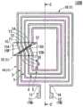
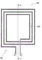
图1是表示第1实施方式所涉及的环形天线110的形状的俯视图。图2是第1实施方式所涉及的环形天线110的图,是沿着A-A’线(跨接线6)的截面图。FIG. 1 is a plan view showing the shape of a
(环形天线)(loop antenna)
如图1所示那样,环形天线110由沿一方向连续地环绕的n圈(n为3以上的整数)的导电布线(环形导电布线1~5)构成。导电布线具备多个环形(环形导电布线),具有在所述多个环形之中的最外周环形或者最内周环形设置的始点13以及终点14。在此,“多个环形”不是指多个环形的每个独立地形成的构件,而是利用公知的成膜工序、光刻技术而一并整体地刻画出的一个导电图案。As shown in FIG. 1 , the
而且,环形天线110具有:环形1~5相连的过渡区域15(后述);与环形1~5以及过渡区域15重叠地设置的绝缘层8;俯视时横穿过渡区域15地设置在绝缘层8上的跨接线6。如图2所示那样,环形天线110形成在基板SB上。另外,基板SB的材料没有特别限定。如后述那样,根据使用环形天线的电子设备的构造,适当地选择基板的材料。Moreover, the
本实施方式所涉及的环形天线110能够使用在车载用环形天线、无线供受电系统等中。The
在本实施方式中,整数n为5,环形天线110具备5圈的环形。环形天线110具有第1个环形1、第2个环形2(第n-3个环形,即第“5-3”个环形)、第3个环形3(第n-2个环形,即第“5-2”个环形)、第4个环形4(第n-1个环形,即第“5-1”个环形)及第5个环形5。In the present embodiment, the integer n is 5, and the
(第1个环形)(1st ring)
第1个环形1是构成环形天线110的多个环形之中位于最外侧的最外周环形(环形导电布线1~5之中最外周的环形)。第1个环形1是多个环形从外侧朝向内侧排列的环形天线110中的成为环绕开始的环形。第1个环形1具有与第1端子11(端子部TM)相连的始点13,构成环形天线110的多个环形在俯视时以从始点13起朝向顺时针方向CW形成环形形状的方式环绕。The
第1个环形1具有端部1E(一部分)和部分1T(位于与端部1E相反的一侧的相反侧部分)。The
第1个环形1具有沿着环形天线110的外形而弯折且延伸的第1分割环形1A和第2分割环形1B。第1分割环形1A连接于始点13和与第2个环形2的部分2E相连的第1个过渡部15A。第2分割环形1B连接于端部1E和与第2端子12(端子部TM)相连的终点14。始点13、终点14、第1端子11及第2端子12位于环形天线110的外侧。The
在本实施方式中,第1个环形1具有位于相互分离且对置的位置的始点13以及终点14,第1个环形1的俯视时的布线构造的点中,始点13与终点14不相连。在本发明中,在环形具有这样的始点和终点的情况下也称作“环形”。In the present embodiment, the
(第2个环形~第4个环形)(2nd circle to 4th circle)
第2个环形2在俯视时沿着第1个环形1弯折且延伸,位于第1个环形1的内侧。第2个环形2具有部分2E(一部分)和部分2T(位于与部分2E相反的一侧的相反侧部分)。The
第3个环形3在俯视时沿着第2个环形2弯折且延伸,位于第2个环形2的内侧。第3个环形3具有部分3E(一部分)和部分3T(位于与部分3E相反的一侧的相反侧部分)。The
第4个环形4在俯视时沿着第3个环形3弯折且延伸,位于第3个环形3的内侧。第4个环形4具有部分4E(一部分)和部分4T(位于与部分4E相反的一侧的相反侧部分)。The
第2个环形2、第3个环形3及第4个环形4是位于第1个环形1与第5个环形5之间的中间环形,中间环形的数量为3个。The
(第5个环形)(5th ring)
第5个环形5是构成环形天线110的多个环形之中位于最内侧的最内周环形(环形导电布线1~5之中的最内周的环形)。第5个环形5具有部分5E(一部分)和端部5T(位于与部分5E相反的一侧的相反侧部分)。The
第5个环形5在俯视时沿着第4个环形4弯折且延伸,位于第4个环形4的内侧。The
关于上述的环形1~5的形状,“弯折且延伸”意思是指环形至少具有弯折部或曲线的线状的形状。此外,该意思还指代在弯折部或曲线中组合了直线的形状。图1所示的例子中,环形1~5分别具有直线,但是也可以采用不具有直线的环形形状。Regarding the shapes of the
(过渡区域)(transition area)
环形天线110具有多个环形相连的过渡区域15。过渡区域15具有第1个过渡部15A、第2个过渡部15B、第3个过渡部15C及第4个过渡部15D。换言之,环形天线110中的过渡部的个数为n-1个,本实施方式中为4个。The
在过渡区域15中,经由过渡部15A~15D的某个,多个环形1~5之中相互相邻的2个环形相连。In the
过渡部15A~15D是相对于后述的横穿的方向31、32倾斜的折弯部分。The
换言之,在过渡区域15中,以随着环形导电布线1~5的环绕,从相对地位于外侧的环形朝向位于内侧的环形过渡的方式,环形导电布线1~5弯折。多个环形依次弯折的部位从位于最外周的第1个环形朝向第n-1个环形排列。此外,沿着后述的方向31、32,多个环形依次弯折。In other words, in the
以下,具体地说明过渡区域15。Hereinafter, the
在过渡区域15的构造中,“向外侧倾斜地弯折”意思是指以向从环形天线110的内侧(最内周环形的位置)朝向外侧(最外周环形的位置)的方向进行偏移的方式过渡部弯折,“向内侧倾斜地弯折”意思是指以向从环形天线110的外侧朝向内侧的方向进行偏移的方式过渡部弯折。In the structure of the
着眼于第1个环形1和第2个环形2则为,第1个过渡部15A(外侧过渡部)从第2个环形2的部分2E(一部分)朝向外侧倾斜地弯折,且连接于在部分2E的外侧相邻地存在的第1个环形1。换言之,第1个过渡部15A(内侧过渡部)从第1个环形1的部分1T(相反侧部分)向内侧倾斜地弯折,且连接于在部分1T的内侧相邻地存在的第2个环形2。Focusing on the
着眼于第2个环形2和第3个环形3则为,第2个过渡部15B(外侧过渡部)从第3个环形3的部分3E(一部分)向外侧倾斜地弯折,且连接于在部分3E的外侧相邻地存在的第2个环形2。换言之,第2个过渡部15B(内侧过渡部)从第2个环形2的部分2T(相反侧部分)向内侧倾斜地弯折,且连接于在部分2T的内侧相邻地存在的第3个环形3。Focusing on the
着眼于第3个环形3和第4个环形4则为,第3个过渡部15C(外侧过渡部)从第4个环形4的部分4E(一部分)向外侧倾斜地弯折,且连接于在部分4E的外侧相邻地存在的第3个环形3。换言之,第3个过渡部15C(内侧过渡部)从第3个环形3的部分3T(相反侧部分)向内侧倾斜地弯折,且连接于在部分3T的内侧相邻地存在的第4个环形4。Focusing on the
着眼于第4个环形4和第5个环形5则为,第4个过渡部15D(外侧过渡部)从第5个环形5的部分5E(一部分)向外侧倾斜地弯折,且连接于在部分5E的外侧相邻地存在的第4个环形4。换言之,第4个过渡部15D(内侧过渡部)从第4个环形4的部分4T(相反侧部分)向内侧倾斜地弯折,且连接于在部分4T的内侧相邻地存在的第5个环形5。Focusing on the
更具体地说明上述的过渡区域15的构造。The structure of the
第1个环形1在俯视时,在与端子部TM(第1端子11及第2端子12)对置的位置(过渡区域15中的部分1T),向环形天线110的环形形状的内侧折弯,连接于第2个环形2。The
第2个环形2在与端子部TM对置的位置(过渡区域15中的部分2T),向环形天线110的环形形状的内侧折弯,连接于第3个环形3。The
第3个环形3在与端子部TM对置的位置(过渡区域15中的部分3T),向环形天线110的环形形状的内侧折弯,在过渡区域15连接于第4个环形4。The
第4个环形4在与端子部TM对置的位置(过渡区域15中的部分4T),向环形天线110的环形形状的内侧折弯,在过渡区域15连接于第5个环形5。The
关于图1所示的环形天线110的形状,“向内侧折弯”意思是指在过渡区域15,环形1~4分别相对于从环形1~4的外形(环形直径)横穿的方向31、32倾斜地折弯。Regarding the shape of the
环形直径是指从环形天线的中心横穿的环形外形的大小,从环形直径横穿的方向也可以是沿着环形天线的短轴的方向,也可以是沿着长轴的方向。因此,从环形直径横穿的方向与环形天线的中心方向同义。The loop diameter refers to the size of the loop shape crossing from the center of the loop antenna, and the direction crossing from the loop diameter may also be along the short axis or along the long axis of the loop antenna. Therefore, the direction transverse from the diameter of the loop is synonymous with the central direction of the loop antenna.
从环形1~4的外形横穿的方向也可以是朝向环形天线110的内侧横穿的方向31、朝向环形天线110的外侧横穿的方向32中的某个。The direction traversing from the outer shape of the
图1所示的环形天线110的相当于环绕结束的环形是第5个环形5(n=5)。始点13沿从环形天线110离开的方向延伸,连接于第1端子11。终点14沿从环形天线110离开的方向延伸,连接于第2端子12。The loop corresponding to the end of the loop of the
第5个环形5的端部5T经由在绝缘层8形成的通孔以及跨接线6而与第1个环形1(最外周环形)的端部1E电连接。端部1E经由第1个环形1的第2分割环形1B而连接于终点14,终点14连接于第2端子12。An
在图1所示的过渡区域15中,过渡部15A~15D分别将环形1~5之中的相互相邻的2个环形电连接。此外,跨接线6将第1个环形1与第5个环形5电连接。In
另外,若环绕圈数超过5,则相对于横穿的方向31、32倾斜地折弯的过渡部的数量增加。Furthermore, if the number of turns exceeds five, the number of transitions bent obliquely with respect to the
也可以是,省掉第1端子11以及第2端子12,环形天线110与包含电容器的电路(后述的天线部、充电控制部、NFC通信部等)电连接。Alternatively, the
本发明中不限定图1所示的环绕圈数5(n=5),只要环绕圈数为3以上即可。一般来讲,若是环绕圈数超过25,则构成环形天线的导电布线的电阻值变大,天线效率容易降低。在将天线用作进行非接触供受电的受电天线的情况下,为了确保受电天线的输出电压,可以将环绕圈数设为3以上25以下的范围。The present invention is not limited to the number of turns 5 (n=5) shown in FIG. 1 , as long as the number of turns is 3 or more. Generally speaking, if the number of turns exceeds 25, the resistance value of the conductive wiring constituting the loop antenna increases, and the antenna efficiency tends to decrease. When the antenna is used as a power receiving antenna for non-contact power supply and reception, the number of turns can be set within a range of 3 to 25 in order to secure an output voltage of the power receiving antenna.
另一方面,在环绕圈数为2以下的情况下,难以确保足够的输出电压。除此之外,在2以下这样的环绕圈数少的情况下,由环形天线产生的磁场分布容易产生偏倚。该情况下,在相互对置的天线中,与供受电、信号的收发(通信)有关的耦合性降低,共振容易变得不稳定。On the other hand, when the number of turns is 2 or less, it is difficult to secure a sufficient output voltage. In addition, when the number of turns is small such as 2 or less, the magnetic field distribution generated by the loop antenna tends to be biased. In this case, in the antennas facing each other, the coupling performance related to power supply/reception and signal transmission/reception (communication) decreases, and resonance tends to become unstable.
若环绕圈数为26以上,则构成环形天线的导电布线的路线长变得过长,由于电阻值的增加而容易导致天线效率降低。If the number of turns is 26 or more, the length of the conductive wiring constituting the loop antenna becomes too long, and the antenna efficiency tends to decrease due to an increase in the resistance value.
另外,作为俯视时的环形天线的外形,也可以采用圆形、椭圆形、矩形、多边形等形状。In addition, as the outer shape of the loop antenna in a plan view, shapes such as a circle, an ellipse, a rectangle, and a polygon may be employed.
(绝缘层)(Insulation)
绝缘层8与环形导电布线及过渡区域15重叠地设置。绝缘层8具有:设置在与第1个环形1的端部1E对应的位置的第1通孔8A;以及设置在与第5个环形5的端部5T对应的位置的第2通孔8B。The insulating
作为构成绝缘层8的材料,例如采用SiO2、SiN等无机材料;丙烯酸、聚酰亚胺等树脂材料;或者印刷基板所使用的树脂材料。绝缘层8的介电常数优选低。As a material constituting the insulating
(跨接线)(jumper wire)
跨接线6以俯视时横穿过渡区域15的方式设置在绝缘层8上,形成在第1通孔8A与第2通孔8B之间。跨接线6在第1通孔8A中与第1个环形1的端部1E电连接,在第2通孔8B中与第5个环形5的端部5T电连接。由此,跨接线6将环形1的端部1E与第5个环形5的端部5T电连接。The
在环形天线110中,跨接线6的根数为1根,通孔(第1通孔8A及第2通孔8B)的个数为2处,较少。因此,能够减轻环形天线110的制造上的负担。In the
如图1所示那样,跨接线6在以横穿的方向31、32为基准、相对于过渡部15A~15D相反的倾斜方向上延伸。具体而言,过渡部15A~15D在从左侧(第1侧)朝向右侧(第2侧)的方向上,朝向环形天线110的内侧(横穿的方向31上)弯折。与此相对,跨接线6在从左侧(第1侧)朝向右侧(第2侧)的方向上,朝向环形天线110的外侧(横穿的方向32上)延伸。As shown in FIG. 1 , the
构成环形天线110的环形1~5及跨接线6由导电布线形成。例如,环形1~5及过渡部15A~15D由在基板SB上形成的导电布线构成,跨接线6由在绝缘层8上形成的导电布线构成。这样的导电布线具有铜层或铜合金层被导电性金属氧化物夹着的3层构成。The
作为3层构成,例如可列举出导电性金属氧化物层/铜合金层/导电性金属氧化物层。本发明不限于这样的构成,也可以使用经由粘合材层叠了铜箔的构成来形成环形天线。也可以取代铜合金层而采用纯铜的层。也可以具有铜合金层被层叠在由镍、钛等迁移金属构成的层、或者含有这些材料的合金层上的构成。在后述的第1通孔8A及第2通孔8B中的、环形1、5与跨接线6的电连接构造中,优选在端部1E、5T的表面,形成由金等贵金属或者含有氧化铟的导电性氧化物构成的层。也可以是在后述的第1端子11、第2端子12的表面,进行金等贵金属镀覆处理或焊镀处理。As a three-layer structure, a conductive metal oxide layer/copper alloy layer/conductive metal oxide layer is mentioned, for example. The present invention is not limited to such a configuration, and a loop antenna may be formed using a configuration in which copper foil is laminated via an adhesive material. Instead of the copper alloy layer, a layer of pure copper may be used. A configuration in which a copper alloy layer is laminated on a layer made of a transition metal such as nickel or titanium, or an alloy layer containing these materials may also be employed. In the electrical connection structure between the
通过采用由金等贵金属或者含有氧化铟的导电性氧化物构成的层,能够以低接触电阻进行电安装。By employing a layer made of a noble metal such as gold or a conductive oxide containing indium oxide, electrical mounting can be performed with low contact resistance.
图23是表示以往的环形天线900的俯视图。FIG. 23 is a plan view showing a
构成环形天线900的最外周环形901以及最内周环形902的形状相对于中心线C-C’非对称。因此,环形天线900的天线的对称性差。The shapes of the
与此相对,图1所示的第1实施方式所涉及的环形天线虽然在过渡区域15中未获得严格的对称性,但是环形1~5除了过渡区域15之外,相对于中心线C-C’对称地配置,得到了相比于以往例的环形天线900被较大地改善了的对称性。在具有高的对称性的环形天线中,磁场被更均匀地生成,伴随于此,容易抑制从环形天线扩散的噪声。磁场的均匀性优异的环形天线在高频带也容易共振。磁场的均匀性较差的环形天线容易产生大的扩散噪声,容易给周边的电子电路或设备带来噪声。In contrast, the loop antenna according to the first embodiment shown in FIG. 'Arranged symmetrically, symmetry is greatly improved compared to the
(第1实施方式的变形例1)(
图3是表示第1实施方式的变形例所涉及的环形天线130A的俯视图。图3中,对与第1实施方式相同的构件赋予相同附图标记,省略或简化其说明。FIG. 3 is a plan view showing a
关于始点及终点配置在环形天线的内侧这一点,本变形例与上述的第1实施方式不同。This modified example is different from the first embodiment described above in that the start point and the end point are arranged inside the loop antenna.
(第1个环形~第4个环形)(1st ring to 4th ring)
第1个环形1在俯视时,以从端部1E起朝向顺时针方向CW形成环形形状的方式环绕。第1个环形1不具有上述的始点13及终点14。第2个环形~第4个环形与上述的第1实施方式同样。The
(第5个环形)(5th ring)
第5个环形5是多个环形从内侧朝向外侧排列的环形天线130A中的成为环绕开始的环形。第5个环形5具有连接于第1端子23(端子部TM)的始点22,构成环形天线130A的多个环形在俯视时,以从始点22起朝向顺时针方向CW形成环形形状的方式环绕。The
第5个环形5具有端部5E(一部分)和部分5T(位于与端部5E相反的一侧的相反侧部分)。The
第5个环形5具有沿着第4个环形4弯折且延伸的第1分割环形5A和第2分割环形5B。第1分割环形5A连接于始点22及跨接线6。第2分割环形5B连接于端部5E和与第2端子24(端子部TM)连接的终点21。始点22、终点21、第1端子23及第2端子24位于环形天线130A的内侧。The
本变形例中,第5个环形5具有位于相互分离且对置的位置的始点22及终点21,在第5个环形5的俯视时的布线构造的点中,始点22与终点21不相连。与上述的实施方式同样,在本发明中,在环形具有这样的始点和终点的情况下也称作“环形”。In this modified example, the
根据本变形例所涉及的环形天线130A,得到与上述的实施方式同样的效果。According to the
具有这样的构造的环形天线130A例如被应用于后述的第6实施方式。另外,本变形例中,也可以不形成第1端子23及第2端子24。环形天线130A能够应用于数据载体、IC卡等中。The
(第1实施方式的变形例2)(
图4是表示第1实施方式的变形例所涉及的环形天线130B的俯视图。图4中,对与第1实施方式相同的构件赋予相同附图标记,省略或简化其说明。关于过渡区域15的形成位置这一点,本变形例与上述的第1实施方式不同。FIG. 4 is a plan view showing a
具体而言,在图1所示的例子中,在环形天线110中,在与端子部TM的配置位置相反的一侧设置有过渡区域15,但在本变形例2中,在环形天线130B的左侧设置有过渡区域15。这样的构成也能够获得与上述的第1实施方式同样的效果。Specifically, in the example shown in FIG. 1 , in the
(第2实施方式)(second embodiment)
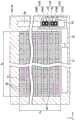
图5是第2实施方式所涉及的环形天线单元的俯视图。图5中,对与第1实施方式相同的构件赋予相同附图标记,省略或简化其说明。5 is a plan view of the loop antenna unit according to the second embodiment. In FIG. 5 , the same reference numerals are assigned to the same components as those in the first embodiment, and description thereof will be omitted or simplified.
(环形天线单元)(loop antenna unit)
本实施方式所涉及的环形天线单元100由具备上述的第1实施方式所涉及的环形天线的构造的2个环形天线110、110’(第1环形天线、第2环形天线)构成。The
2个环形天线110、110’具有相互相同的环绕圈数,环绕方向相互不同。在俯视时,2个环形天线110、110’配置在相互不重叠的线对称的位置。The two
具体而言,环形天线110具有从始点13起向顺时针方向CW(第1方向)环绕的环形1~5。环形天线110’具有从始点13’起向逆时针方向ACW(第2方向)环绕的环形1’~5’。环形1’~5’就环绕方向这一点与环形1~5不同,但是其他构造、材料等这些点与环形1’~5’相同。Specifically, the
环形天线110包括:具有过渡部15A~15D的过渡区域15;以及跨接线6。环形天线110’包括:具有过渡部16A~16D的过渡区域16;以及跨接线7。过渡部16A~16D及跨接线7配置在相对于中心线C-C’与过渡部15A~15D及跨接线6线对称的位置。关于该点,过渡部16A~16D及跨接线7与过渡部15A~15D及跨接线6不同,但其他构造、材料等这些点与过渡部15A~15D及跨接线6相同。The
第2实施方式如图5所示那样,示出了由2个环形天线110、110’构成了一组的环形天线单元100的例子,但是构成一个环形天线单元的环形天线的数量不限于2。也可以是由3个以上的环形天线来构成1个环形天线单元。该情况下,2个环形天线的环绕方向相互相反。In the second embodiment, as shown in FIG. 5 , an example of a
本实施方式所涉及的环形天线单元100具有将上述的第1实施方式所示的2个环形天线以成为相对于中心线C-C’线对称的形状的方式排列而成的构造。过渡区域15、16中的过渡部15A~15D以及过渡部16A~16D具有稍微复杂的形状,易成为噪声产生源。然而,通过将构成过渡区域15的过渡部15A~15D与构成过渡区域16的过渡部16A~16D以具有线对称的形状的方式形成,从而能够将从过渡区域15、16产生的噪声抵消,能够抑制天线中的噪声产生。The
通过调整构成环形天线110的环形的间距P1、构成环形天线110’的环形的间距P2及环形天线110、110’间的间隙Gap的宽度,能够调整环形天线的耦合。通过将环形天线110、110’以相互接近的方式配置,能够提高与中心线C-C’接近的位置处的磁场的强度。The coupling of the loop antenna can be adjusted by adjusting the pitch P1 of the loops constituting the
在作为进行非接触供受电的天线而使用第2实施方式所涉及的环形天线单元100的情况下,环形天线单元100能够作为受电天线使用,并且,也能够作为供电天线使用。在被称作充电底座(cradle)的供电台,也可以将多个环形天线单元100例如以矩阵状配设。When the
另外,构成环形天线单元100的环形天线110、110’分别具备未图示的电容元件(电容器),与驱动环形天线110、110’的电源并联连接。In addition, the
(第3实施方式)(third embodiment)
图6是表示第3实施方式所涉及的环形天线单元的俯视图。图6中,对与第2实施方式相同的构件赋予相同附图标记,省略或简化其说明。6 is a plan view showing a loop antenna unit according to a third embodiment. In FIG. 6 , the same reference numerals are assigned to the same components as those in the second embodiment, and description thereof will be omitted or simplified.
(环形天线单元)(loop antenna unit)
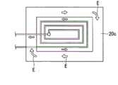
第3实施方式所示的环形天线单元200不仅具有第2实施方式所示的环形天线单元100,还具备将环形天线110、110’的周围局部地包围的导电图案20(将环形天线110、110’的周围的一部分包围的导电图案)。The
导电图案20具有大致U字状的形状,在大致U字形状的内侧配置有2个环形天线110、110’。The
具体而言,导电图案20具有与环形天线110、110’的双方对置的背部20A;以及位于背部20A的两侧的2个侧部20B。2个侧部20B当中,一方的侧部20B(第1侧部)与环形天线110的第1个环形1(最外周环形)对置,另一方的侧部20B(第2侧部)与环形天线110’的第1个环形1’(最外周环形)对置。2个侧部20B在与背部20A的延伸方向正交的方向上延伸,连接于背部20A。在2个侧部20B,在与连接于背部20A的部分相反的一侧形成有端部20BT,在2个侧部20B的端部20BT之间形成有开口20D。通过形成开口20D,导电图案20不是将环形天线110、110’的整周包围。Specifically, the
具有这样的构成的环形天线单元200在电流量多的电子部件配置在环形天线单元200附近的情况下是有效的。
通过将导电图案20的背部20A朝向电流量多的电子部件的方向,即,通过在电子部件与环形天线110、110’之间配置背部20A,能够减少噪声对环形天线110、110’的影响。关于将环形天线单元的周围的一部分用导电图案20进行了包围的环形天线单元,留待后述。The influence of noise on the
另外,导电图案20如图6所示那样,需要是一部分敞开的图案(不是电闭合的图案,而是不电相连的图案)。在图24所示那样的电相连的导电图案20c中,受到在导电图案20c的周围配置的电子部件(外部)的电流或磁场等的影响,容易产生涡流E。该涡流E成为使位于导电图案20c内部的天线产生相反朝向的电流的噪声源。In addition, as shown in FIG. 6 , the
(第4实施方式)(fourth embodiment)
图7是第4实施方式所涉及的环形天线单元的俯视图。图7中,对与第3实施方式相同的构件赋予相同附图标记,省略或简化其说明。7 is a plan view of a loop antenna unit according to a fourth embodiment. In FIG. 7 , the same reference numerals are assigned to the same components as those in the third embodiment, and description thereof will be omitted or simplified.
(环形天线单元)(loop antenna unit)
第4实施方式所涉及的环形天线单元300与第3实施方式同样,具备将环形天线110、110’的周围局部地包围的导电图案20。关于过渡区域15、16的配置这一点,第4实施方式与第3实施方式不同。Like the third embodiment, the
具体而言,在第3实施方式所涉及的环形天线单元200中,在与背部20A对置的位置配置有过渡区域15、16。与此相对,在第4实施方式所涉及的环形天线单元300中,在与2个侧部20B对置的位置配置有过渡区域15、16。Specifically, in the
环形天线单元300的其他构造与环形天线单元200相同。在本实施方式中,由环形天线单元300得到的效果与第3实施方式的环形天线单元200几乎等价。Other configurations of the
(第5实施方式)(fifth embodiment)
图8是表示第5实施方式所涉及的环形天线单元的俯视图。图8中,对与上述的实施方式相同的构件赋予相同附图标记,省略或简化其说明。8 is a plan view showing a loop antenna unit according to a fifth embodiment. In FIG. 8 , the same reference numerals are assigned to the same components as those in the above-mentioned embodiment, and description thereof will be omitted or simplified.
(环形天线单元)(loop antenna unit)
第5实施方式所涉及的环形天线单元800具有相互相邻的2个环形天线810(第1环形天线)及环形天线820(第2环形天线)。The
2个环形天线810、820具有相互相同的环绕圈数,环绕方向相互不同。在俯视时,2个环形天线810、820配置在相互不重叠的线对称的位置。The two
关于构成环形天线的环形的密度的这一点,第5实施方式与第2实施方式不同。The fifth embodiment differs from the second embodiment in terms of the density of loops constituting the loop antenna.
具体而言,环形天线810具有以顺时针方向CW连续地环绕的多个环形811~815。环形天线820具有以逆时针方向ACW连续地环绕的多个环形821~825。Specifically, the
在环形天线810、820各自中,在位于与中心线C-C’接近的位置的内侧区域HD,环形的布线密度高,在从中心线C-C’远离的外侧区域LD,环形的布线密度变低。In each of the
在此,布线密度是指每单位面积中的多个环形的合计的长度。或者,布线密度是指俯视时从多个环形横穿的方向(与中心线C-C’垂直的方向)上的每单位宽度中的多个环形的根数。Here, the wiring density refers to the total length of a plurality of loops per unit area. Alternatively, the wiring density refers to the number of multiple loops per unit width in a direction across the multiple loops (direction perpendicular to the center line CC') in plan view.
因此,在每单位面积中的多个环形的合计的长度大的区域(内侧区域HD),布线密度高。或者,在俯视时从多个环形横穿的方向上的每单位宽度中的多个环形的根数少的区域(外侧区域LD),布线密度低。Therefore, the wiring density is high in the region (inner region HD) where the total length of the plurality of loops per unit area is large. Alternatively, the wiring density is low in a region (outer region LD) with a small number of loops per unit width in a direction across the loops in a plan view.
在布线密度低的外侧区域LD,形成低密度的磁通,伴随于此,能够抑制噪声向环形天线单元800周围的扩散。通过形成布线密度低的外侧区域LD,能够抑制环形天线810和环形天线820中的寄生电容的产生。除此之外,由于相互相邻的环形天线810与环形天线820相对于心线C-C’对称地配置,因此,通过天线的对称性能够获得将噪声扩散抵消的效果,能够抑制噪声向环形天线单元800外部的扩散。In the outer region LD where the wiring density is low, a low-density magnetic flux is formed, and accordingly, diffusion of noise around the
此外,与中心线C-C’接近的区域(内侧区域HD)中的环形天线810与环形天线820的磁场耦合提高。因此,在作为进行非接触供受电的受电天线或供电天线而使用环形天线单元800的情况下,能够提高环形天线单元800相对于充电底座(充电台)的供受电效率。通过设置多个环形的布线密度低的外侧区域LD、以及多个环形的布线密度高的内侧区域HD,能够获得容易扩展频带的效果。能够获得充电底座与环形天线单元800之间的位置偏移被允许的余地(margin),能够提高供受电的效率。通过环形天线单元800具有布线密度低的外侧区域LD,能够减少环形天线810及环形天线820各自中的寄生电容,能够提高供受电的效率。In addition, the magnetic field coupling between the
如图8所示那样,相互相邻的环形天线810、820在俯视时以中心线C-C’为轴而对称地配置。对环形天线单元800从外部观察时,确保了磁场放射的均匀性,容易确保平衡性。除此之外,通过2个环形天线810、820相邻,从而相对于中心线C-C’对称的磁场耦合变得容易。As shown in FIG. 8 , the
而且,通过在与中心线C-C’垂直的方向上改变构成小径环形天线的多个环形的布线密度,从而容易使磁场分布偏靠向环形天线单元800的中心。或者,通过设置多个环形的布线密度不同的部分(内侧区域HD,外侧区域LD),能够扩展共振的频带。此外,通过使磁场分布偏靠向与中心线C-C’接近的位置,例如,能够顺畅地进行为了充电而使用了具备多个天线的充电底座(充电台)的充电。换言之,相对于充电底座中配设的多个天线的共振性提高,充电底座与多个天线之间的对位的余地(位置偏移被允许的余地)扩大。Furthermore, by changing the wiring density of the plurality of loops constituting the small-diameter loop antenna in a direction perpendicular to the centerline CC', the magnetic field distribution can be easily shifted toward the center of the
另外,在本实施方式所涉及的环形天线单元800中,也可以是,设置将2个环形天线810、820局部地包围并且具有大致U字状的形状的导电图案20。In addition, in the
(第6实施方式~第8实施方式)(Sixth Embodiment to Eighth Embodiment)
第6实施方式~第8实施方式所涉及的电子设备包括:智能手机、平板、笔记本PC等通信终端;智能手表、智能眼镜等可穿戴终端;摄像机;游戏机;电子纸张;具有显示器部的IC卡或存储卡等数据载体;以及个人认证设备等具有通信功能的信息介质。第6实施方式~第8实施方式所涉及的电子设备包括具备TV或广告介质等的显示部的显示功能、并且具备静电电容方式的输入功能的电子设备。从携带或操作的简便性的观点出发,优选这样的电子设备中搭载有非接触充电功能。Electronic devices according to the sixth to eighth embodiments include: communication terminals such as smartphones, tablets, and notebook PCs; wearable terminals such as smart watches and smart glasses; video cameras; game machines; electronic paper; data carriers such as cards or memory cards; and information media with communication functions such as personal authentication devices. The electronic devices according to the sixth to eighth embodiments include electronic devices having a display function of a display unit such as a TV or an advertisement medium, and also having a capacitive input function. From the viewpoint of portability and ease of operation, it is preferable that such an electronic device is equipped with a non-contact charging function.
在以下描述的第6实施方式~第8实施方式中,对特征性部分进行说明,例如对于通常的电子设备中使用的构成要素与后述的实施方式所涉及的电子设备没有差异的部分,有时省略说明。In the sixth to eighth embodiments described below, the characteristic parts will be described. For example, there may be cases where there is no difference between the components used in ordinary electronic equipment and the electronic equipment related to the embodiments described later. Description omitted.
第1基板、第2基板、第1布线、第2布线、第3布线等、或者第1导电性金属氧化物层以及第2导电性金属氧化物层等中使用的“第1”、“第2”等序数词是为了避免构成要素的混同而附加的,并不限定数量。此外,第1导电性金属氧化物层以及第2导电性金属氧化物层在以下的说明中有时仅简称为导电性金属氧化物层。"First" and "first" used in the first substrate, the second substrate, the first wiring, the second wiring, the third wiring, etc., or the first conductive metal oxide layer and the second conductive metal oxide layer, etc. Ordinal numerals such as 2" are added to avoid confusion of constituent elements, and the number is not limited. In addition, the first conductive metal oxide layer and the second conductive metal oxide layer may be simply referred to simply as conductive metal oxide layers in the following description.
此外,后述的电子设备具备与上述的第2实施方式~第5实施方式所涉及的环形天线单元相当的第1天线单元、第2天线单元、第3天线单元、第4天线单元及第5天线单元。以下说明的实施方式中,有时将第1~第5天线单元仅称作天线单元,并且有时将环形天线称作天线。本发明的实施方式所涉及的天线单元与环形天线单元同义。In addition, electronic equipment described later includes a first antenna unit, a second antenna unit, a third antenna unit, a fourth antenna unit, and a fifth antenna unit corresponding to the loop antenna units according to the second to fifth embodiments described above. Antenna unit. In the embodiments described below, the first to fifth antenna units may be referred to simply as antenna units, and the loop antenna may be referred to as antennas. The antenna unit according to the embodiments of the present invention is synonymous with the loop antenna unit.
在第6实施方式~第8实施方式所涉及的电子设备具有显示器部的情况下,作为构成显示器部的显示功能层,能够使用被称作LED(Light Emitting Diode)的多个发光二极管元件、也被称作OLED的多个有机EL(有机电致发光)元件、或者液晶层。When the electronic devices according to the sixth to eighth embodiments have a display unit, a plurality of light emitting diode elements called LED (Light Emitting Diode), or A plurality of organic EL (Organic Electroluminescent) elements called OLEDs, or a liquid crystal layer.
有机EL元件是在一对电极间被施加了电场时通过从阳极(例如,上部电极)注入的空穴与从阴极(例如,下部电极、像素电极)注入的电子再结合而产生激励、以像素单位进行发光的、使用了有机材料的显示功能层。有机EL的情况下的显示功能层含有具有发光性质的材料(发光材料),并且,优选含有具有电子输送性的材料。发光层是形成在阳极与阴极之间的层,在下部电极(正极)上形成有空穴注入层的情况下,在空穴注入层与上部电极(负极)之间形成发光层。此外,在阳极上形成有空穴输送层的情况下,在空穴输送层与阴极之间形成发光层。上部电极与下部电极的作用能够更换。The organic EL element is excited by the recombination of holes injected from the anode (for example, upper electrode) and electrons injected from the cathode (for example, lower electrode, pixel electrode) when an electric field is applied between a pair of electrodes, and the pixel A display function layer using an organic material that emits light in units. The display functional layer in the case of organic EL contains a material having light emitting properties (light emitting material), and preferably contains a material having electron transport properties. The light emitting layer is a layer formed between the anode and the cathode, and when the hole injection layer is formed on the lower electrode (positive electrode), the light emitting layer is formed between the hole injection layer and the upper electrode (negative electrode). In addition, when a hole transport layer is formed on the anode, a light emitting layer is formed between the hole transport layer and the cathode. The role of the upper electrode and the lower electrode can be replaced.
LED具有与有机EL元件同样的电极构造,此外,LED(显示功能层、发光层)的驱动与有机EL元件同样地进行。LED使用氮化铟镓(InGaN)、氮化镓(GaN)、氮化铝镓(AlGaN)、砷化铝镓(AlGaAs)、磷砷化镓(GaAsP)、磷化镓(GaP)等、化合物半导体的单层或层叠构成。The LED has the same electrode structure as the organic EL element, and the drive of the LED (display function layer, light-emitting layer) is performed in the same manner as the organic EL element. LED uses indium gallium nitride (InGaN), gallium nitride (GaN), aluminum gallium nitride (AlGaN), aluminum gallium arsenide (AlGaAs), gallium arsenide phosphide (GaAsP), gallium phosphide (GaP), etc., compounds A single layer or stack of semiconductors.
如后述那样,作为上述化合物半导体的构造,通过n型半导体层/发光层/p型半导体层的层叠构成而被使用的情况较多。在LED的电极构造中,已知有在上述层叠构成的单侧的面上正极与负极并列地配置的构造,换言之,在水平方向上这些电极并列地配置的水平型发光二极管。或者,已知有上部电极/n型半导体层/发光层/p型半导体层/下部电极在与厚度垂直的方向上层叠的垂直型发光二极管。在垂直型发光二极管中,上部电极与下部电极配设在不同面。如以上那样,LED的发光层由无机材料构成。As will be described later, as the structure of the above-mentioned compound semiconductor, a laminated structure of n-type semiconductor layer/light-emitting layer/p-type semiconductor layer is often used. Among the electrode structures of LEDs, there is known a structure in which a positive electrode and a negative electrode are arranged in parallel on one side of the above-mentioned laminated structure, in other words, a horizontal light emitting diode in which these electrodes are arranged in parallel in the horizontal direction. Alternatively, there is known a vertical light emitting diode in which an upper electrode/n-type semiconductor layer/light emitting layer/p-type semiconductor layer/lower electrode are stacked in a direction perpendicular to the thickness. In the vertical light emitting diode, the upper electrode and the lower electrode are disposed on different surfaces. As described above, the light-emitting layer of the LED is made of an inorganic material.
第6实施方式~第8实施方式所涉及的电子设备中可应用的基板无需限定为透明的基板。例如,作为后述的第1基板、第2基板、第3基板中可应用的基板,可列举出玻备中。还可以在由这样的树脂构成的基板中加入玻璃纤维等填料。还能够由使用经由粘合材而层压了铜箔的环氧树脂构成的基板,利用使用刻蚀剂的公知的光刻手法,来形成天线图案。在非接触IC卡那样的卡状的电子设备使用上述的实施方式所涉及的环形天线的情况下,作为树脂基板也可以采用使用了聚氯乙烯的基板。The substrates applicable to the electronic devices according to the sixth to eighth embodiments are not necessarily limited to transparent substrates. For example, examples of substrates applicable to the first substrate, second substrate, and third substrate described later include glass equipment. A filler such as glass fiber may also be added to a substrate made of such a resin. An antenna pattern can also be formed by using a substrate made of epoxy resin on which copper foil is laminated via an adhesive material, by a known photolithography method using an etchant. When the loop antenna according to the above-mentioned embodiment is used in a card-shaped electronic device such as a non-contact IC card, a substrate using polyvinyl chloride may be used as the resin substrate.
在将具备上述的实施方式所涉及的环形天线的天线单元应用于电子设备的构成中,能够将天线单元形成在多层的树脂层之间,或者多层的陶瓷层之间。在具有这样的构成的电子设备中,能够以非接触的方式收发各种电信号,或者进行电子设备的驱动所需的电力的送受电。或者,形成有天线的基板也可以是分散有铁氧体等的磁性体。In a configuration in which the antenna unit including the loop antenna according to the above-described embodiment is applied to an electronic device, the antenna unit can be formed between multiple resin layers or between multiple ceramic layers. In an electronic device having such a configuration, various electric signals can be transmitted and received in a non-contact manner, and electric power necessary for driving the electronic device can be transmitted and received. Alternatively, the substrate on which the antenna is formed may be a magnetic substance in which ferrite or the like is dispersed.
在考虑将需要热扩散的LED或有机EL等发光元件应用于电子设备的情况下,为了避免蓄热,优选为,电子设备中使用的基板的热传导率κ(W/m·K)大于1。通常的玻璃基板的热传导率为0.5~0.8W/m·K前后,优选将具有比该热传导率更好的热传导率的强化玻璃、石英基板、蓝宝石玻璃等作为在第6实施方式~第8实施方式所涉及的电子设备中使用的基板。When considering the application of light-emitting elements such as LEDs and organic ELs that require thermal diffusion to electronic devices, it is preferable that the thermal conductivity κ (W/m·K) of the substrate used in the electronic device is greater than 1 in order to avoid heat storage. The thermal conductivity of a general glass substrate is around 0.5 to 0.8 W/m·K, and it is preferable to use tempered glass, quartz substrate, sapphire glass, etc. having a thermal conductivity higher than this thermal conductivity as the sixth embodiment to the eighth embodiment. way involves substrates used in electronic devices.
在第6实施方式~第8实施方式所涉及的电子设备中使用的基板上形成的布线、例如第1导电布线、第2导电布线、驱动薄膜晶体管的源极布线、栅极布线、电源线及包含天线的布线,优选使用热传导性良好的铜布线或者铜合金布线。在形成LED或有机EL等发光元件(发光二极管元件)的第2基板的第4面,优选在导电性屏蔽层的构成中包含热传导性良好的金属层或者热传导性良好的光吸收层。Wirings formed on the substrates used in the electronic devices according to the sixth to eighth embodiments, such as first conductive wiring, second conductive wiring, source wiring, gate wiring, power supply lines and For wiring including the antenna, it is preferable to use copper wiring or copper alloy wiring with good thermal conductivity. On the fourth surface of the second substrate on which light-emitting elements (light-emitting diode elements) such as LEDs and organic ELs are formed, it is preferable to include a metal layer with good thermal conductivity or a light-absorbing layer with good heat conductivity in the configuration of the conductive shield layer.
(第6实施方式)(sixth embodiment)
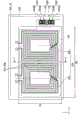
图9是第6实施方式所涉及的电子设备的俯视图,示出了应用了图3所示的环形天线的构造。在本实施方式中,作为电子设备,使用被称作非接触IC卡的数据载体。在图9中,对与上述的实施方式相同的构件赋予相同附图标记,省略或简化其说明。9 is a plan view of an electronic device according to a sixth embodiment, showing a structure to which the loop antenna shown in FIG. 3 is applied. In this embodiment, a data carrier called a non-contact IC card is used as an electronic device. In FIG. 9 , the same reference numerals are assigned to the same components as those in the above-mentioned embodiment, and description thereof will be omitted or simplified.
电子设备400例如具备在由聚氯乙烯树脂等树脂薄膜构成的基板700上形成有环形天线410、天线电源部411、控制部412、存储器413、充电控制部414及二次电池415的构造。二次电池415例如是锂电池或大容量电容器。与以往已知的多数IC卡的构造同样,也可以从电子设备400省去充电控制部414以及二次电池415。天线电源部411中包括进行13.56MHz等的与IC卡读写器之间的通信(共振)控制的同步电路、整流电路等。通信所使用的频率不限于13.56MHz,也可以使用多个频带。也可以使用比13.56MHz高的频率。
环形天线410是通过对在基板700上形成的具有几μm至几十μm的厚度的铜箔进行图案刻画,从而由具有3至25的范围的环绕圈数的导电布线构成。例如,将天线电源部411、控制部412、存储器413等被集成的IC芯片,例如安装于基板700上。而且,在安装后,利用聚氯乙烯树脂等进行层压处理,以成为所希望的形状的方式对基板700的端面进行加工,得到作为IC卡的电子设备400。The
(第7实施方式)(seventh embodiment)
图10是表示第7实施方式所涉及的电子设备的构成的框图。图11是表示构成第7实施方式所涉及的电子设备的环形天线单元被设置的第2基板的俯视图。图12是表示构成第7实施方式所涉及的电子设备的环形天线单元被设置的第3基板的俯视图。图10至图12中,对与上述的实施方式相同的构件赋予相同附图标记,省略或简化其说明。FIG. 10 is a block diagram showing the configuration of an electronic device according to a seventh embodiment. 11 is a plan view showing a second substrate on which a loop antenna unit constituting an electronic device according to a seventh embodiment is provided. 12 is a plan view showing a third substrate on which a loop antenna unit constituting an electronic device according to a seventh embodiment is provided. In FIGS. 10 to 12 , the same reference numerals are assigned to the same components as those in the above-mentioned embodiment, and description thereof will be omitted or simplified.
(电子设备的功能构成)(Functional configuration of electronic equipment)
如图10所示那样,电子设备500具备第1基板701、第2基板702及第3基板703。从观察方向观察的俯视时,第1基板701、第2基板702及第3基板703依次层叠。As shown in FIG. 10 , the
第1基板701具备第1面41和第2面42。第2基板702具备第3面43和第4面44。第3基板703具备第5面45和第6面46。The
(显示部)(display part)
显示部140设置在第1基板701的第2面42与第2基板702的第3面43之间,包括显示功能层141、显示功能驱动部142及第3天线单元530。The
显示功能层141例如是液晶层,显示功能驱动部142是在第2基板702上以矩阵状配设的有源元件(TFT)阵列。作为构成液晶层的液晶,能够应用扭曲向列型、宾主型、高分子分散型液晶等各种液晶。The
在第1基板701及第2基板702之中的一方,形成有具有由红、绿、蓝构成的多个着色图案的滤色片。滤色片可以包括靛蓝、品红、黄色、白色,也可以是靛蓝、品红、黄色的补色滤色片。On one of the
(系统控制部)(System Control Department)
系统控制部150设置在第2基板702与第3基板703之间,包括天线部151、充电控制部152、切换部153、NFC通信部154(Near Field Communication)、CPU155(CentralProcessing Unit)及第2天线单元520。The
在本实施方式中,系统控制部150是对显示部140中的显示功能、通信功能及非接触充电功能进行控制的控制部。此外,如后述那样,二次电池156设置在系统控制部150的邻接的位置。In the present embodiment,
系统控制部150在显示部140与系统控制部150之间,如附图标记TR23的箭头所示那样,经由第3天线单元530及第2天线单元520,非接触地进行与显示功能层的驱动有关的各种信号的收发,并且,非接触地进行显示功能层的驱动所需的电力的供给及接受。The
CPU155与二次电池156、第2天线单元520、充电控制部152、切换部153及NFC通信部154电连接。充电控制部152以及NFC通信部154与切换部153电连接。天线部151与充电控制部152、切换部153及NFC通信部154电连接。
第2天线单元520相对于构成显示部140的有源元件阵列进行影像信号的收发和电力送电。The
天线部151具备第1天线单元510,该第1天线单元510具有第2实施方式所示的形状,以线对称配设有环形天线。The
充电控制部152如附图标记TR56的箭头所示那样,经由设置于天线部151的第1天线单元510,接受从100V等外部电源(图10中的AC适配器158或充电底座159)供给的电力。充电控制部152包含整流功能、二次电池156的电压监视功能,从充电控制部152将电力向二次电池156供给而使其进行充电。The charging
天线部151具备由环绕方向相互不同的一对环形天线构成的第1天线单元510,具有调整共振所使用的电容器、环形天线的线圈长等的功能。切换部153从系统控制部150接收信号,进行天线部151的受电功能与近距离通信(NFC通信)功能之间的切换。The
在由天线部151进行的受电中,能够采用基于Qi规格的频率。例如,能够使用100KHz至200KHz的频率。或者,由天线部151进行的受电能够应对今后预计的无线充电的国际标准规格。作为使用了天线部151的近距离通信的共振频率,例如能够采用13.56MHz或者比该频率高的频率。近距离通信由NFC通信部154控制。NFC通信部154具有用于进行近距离通信的调制解调功能。For power reception by the
(外部电源)(External power supply)
图10所示的充电底座159具有对第7实施方式所涉及的电子设备500、智能手机等移动终端、可穿戴设备进行充电的功能,作为电力供电部发挥功能。充电底座159具备电磁感应方式的多个供电侧天线157,电子设备500能够从这些1个以上供电侧天线157非接触地接受电力供给。充电底座159具有用于选择多个供电侧天线157中的某个的天线切换部。充电底座159例如经由AC适配器158而与100V、220V等的外部电源连接。The charging
(二次电池)(secondary battery)
二次电池156在第2基板702与第3基板703之间,设置在与系统控制部150邻接的位置。The
作为二次电池156,可列举出锂电池、镍氢电池、有机自由基电池、铅电池、锂空气电池、镍锌电池、镍镉电池、银锌电池等。例如,也可以采用利用外装构件对尼龙、铝等的金属层、环戊二烯(CPP)、电极、隔膜、电解液等进行层压而成的层压型的锂电池。优选将全固体型的锂电池、例如锂硫电池等二次电池应用于二次电池156。此外,能够在从空间(基板间的厚度)的观点来看难以设置二次电池156的、第1基板的第2面上及第2基板的第3面上,例如具备大容量的电容器。在大容量的电容器的构成中能够使用利用真空成膜等方法成膜出的薄膜。Examples of the
在二次电池156中设置有温度传感器,在充电控制部152检测到温度异常的情况下,充电控制部152停止对二次电池156的电力供给(送受电)。A temperature sensor is provided in
图10所示的第1基板701、第2基板702及第3基板703中使用的基板不必限定为透明的基板。例如,作为第1基板701、第2基板702及第3基板703中可应用的基板,可列举出玻璃基板、石英(包含人工石英)基板、蓝宝石基板、陶瓷基板等。第2基板702以及第3基板703可以透明,也可以是不透明的基板、着色的基板。还能够使用聚酰亚胺、聚对苯二甲酸乙二醇酯、聚醚砜、聚醚醚酮、聚丙烯四氟乙烯、聚酰胺、聚碳酸酯等树脂基板。第3基板703也可以由镁合金等的金属形成。The substrates used for the
(第1基板)(1st substrate)
在图10所示的第1基板701的第1面41上,例如能够层叠相位差板、偏光板等光学元件、触摸面板、罩玻璃、防反射膜等。在第1基板701的第2面42上,例如也可以形成滤色片、相位差层、透明电极及取向膜等。On the
(第2基板)(2nd substrate)
如图10所示那样,在第2基板702的第3面43上,至少配设有包含有源元件阵列(TFT阵列、薄膜晶体管阵列)的显示功能驱动部142及第3天线单元530。在显示功能驱动部142中,有源元件阵列驱动作为液晶层的显示功能层141。显示功能层141配设在第1基板701的第2面42与第2基板702的第3面43之间。As shown in FIG. 10 , on the
也可以是,在有源元件阵列上,反射可见光的像素电极(以下称作反射电极)、取向膜形成在与有源元件(TFT)对应的位置。反射电极能够由反射可见域的光(外光)的铝、银或者银合金形成。在将银或银合金用于反射电极的情况下,优选为,以具有[导电性金属氧化物层/银合金层/导电性金属氧化物层]这样的层构成的方式,使用由导电性金属氧化物夹着银合金层的构造。Alternatively, on the active element array, pixel electrodes that reflect visible light (hereinafter referred to as reflective electrodes) and alignment films may be formed at positions corresponding to the active elements (TFTs). The reflective electrode can be formed of aluminum, silver, or a silver alloy that reflects light in the visible region (external light). In the case of using silver or silver alloy for the reflective electrode, it is preferable to use a layer made of a conductive metal oxide layer with a layer configuration of [conductive metal oxide layer/silver alloy layer/conductive metal oxide layer]. A structure in which silver alloy layers are sandwiched between oxides.
另外,第7实施方式所涉及的电子设备500也可以是如下的透射式液晶显示装置:由ITO等透明导电膜形成反射电极,在第2基板702的里面的位置插入了LED等背光灯单元。In addition, the
如图11所示那样,在Ax-Ay所示的有效显示区域,配设有由多个源极布线66和多个栅极布线69划分的多个像素开口部PX(像素)。在多个像素开口部PX分别形成有未图示的有源元件(薄膜晶体管阵列)。多个源极布线66分别与包含移位寄存器、视频线、模拟开关的源极信号开关电路26连接。多个栅极布线69分别与包含移位寄存器的栅极信号开关电路27连接。源极信号开关电路26、栅极信号开关电路27接收从作为显示控制部的系统控制部150输出的信号,控制作为显示功能层141的液晶层。As shown in FIG. 11 , a plurality of pixel openings PX (pixels) partitioned by a plurality of source wirings 66 and a plurality of gate wirings 69 are arranged in the effective display region indicated by Ax-Ay. Active elements (thin film transistor arrays) not shown are formed in the plurality of pixel openings PX, respectively. The plurality of source wirings 66 are respectively connected to the source
(第3天线单元)(3rd Antenna Unit)
图11所示的第3天线单元530具有2个(2组)的由环绕方向相互不同的一对环形天线构成的1组天线单元,即,包括由一对环形天线构成的电力受电部35、以及由一对环形天线构成的影像信号接收部36。The
电力受电部35具有由环形天线535A和相对于环形天线535A线对称地配置且反向环绕的环形天线535B构成的一对环形天线。环形天线535A、535B构成电力受电天线单元535。
影像信号接收部36具有由环形天线536A和相对于环形天线536A线对称地配置且反向环绕的环形天线536B构成的一对环形天线。环形天线536A、536B构成影像信号接收天线单元536。The video
这样的电力受电天线单元535及影像信号接收天线单元536具有与上述的第3实施方式所涉及的天线单元200同样的构造。但是,在本实施方式中,能够采用第4实施方式所涉及的天线单元300、第5实施方式所涉及的天线单元800。Such power receiving
电力受电部35由第1电源控制部59控制。第1电源控制部59至少包含频率整合功能及整流功能。显示控制部28接受从第1电源控制部59供给的电力,控制栅极信号开关电路27、源极信号开关电路26。The electric
在第2基板702的第3面43上配设的第3天线单元530与在后述的第3基板703的第5面45上配设的第2天线单元520,例如以±3μm以内的位置精度重叠。在此“重叠”是指在从观察者P观察电子设备500的观察方向观察的俯视时,第3天线单元530与第2天线单元520为相同的形状,且配置在相同的位置。The
(第3基板)(3rd substrate)
如图12所示那样,在第3基板703的第5面45上,至少配设有第1天线单元510、第2天线单元520、系统控制部150、二次电池156等。As shown in FIG. 12 , at least the
如上述那样,在俯视时,第2天线单元520配设在与第3天线单元530重叠的位置。As described above, the
第1天线单元510具有电子设备500的外部与内部之间的通信功能及电子设备500的从外部的非接触充电功能。第2天线单元520相对于第3天线单元530进行通信、供电及受电。The
在从观察方向观察的俯视时,第2天线单元520及第3天线单元530重叠,第1天线单元510与第3天线单元530不重叠。In plan view from the viewing direction, the
(第1天线单元)(1st Antenna Unit)
第1天线单元510具有由环形天线531和相对于环形天线531线对称地配置且反向环绕的环形天线532构成的一对环形天线。The
第1天线单元510优选以覆盖第1天线单元510的方式具备磁性体层。二次电池156的大小是比磁性体层稍微小的大小较好。The
在第1天线单元510中,例如也可以采用在聚酰亚胺等薄膜上形成粘合层、对在粘合层上形成的铜箔以具有图12所示的天线形状的方式进行加工、进而将分散有铁氧体等磁性体的磁性体层贴合于第1天线单元510的构成。In the
例如,在充电底座159与第1天线单元510共振时,位于环形天线531与环形天线532相邻的部分的环形537、538在相同的方向上流动电流。具体而言,环形537、538中流动的电流包括如图12所示那样向上方流动的情况和向与如图12所示的方向反向的下方流动的情况。即,环形537、538中流动的电流,交错地改变流动方向。向相同方向在环形中流动的电流促进环形天线531与环形天线532之间的电磁耦合,有助于与充电底座159的天线之间的共振的改善,此外,还能产生吸收第1天线单元510与充电底座159的天线之间的位置偏移的作用。For example, when the charging
构成第1天线单元510的环形天线531、532是在相同平面上形成以具有环形形状的方式环绕的螺旋状的导电布线而得的。此外,也可以具有能够相对于第5面45进行平面安装的环形天线形状。环形天线531、532的环绕圈数例如能够从3至25的范围选择。图12所示的环形天线531、532的环绕圈数设为5。作为环形天线的环绕圈数,能够根据共振频率的选择、最适于共振的天线的阻抗设定,选择符合条件的环绕圈数。构成第1天线单元510的环形天线531、532的各自的天线单元面积优选较大。图12所示的附图标记Bx、By所示的部分的面积相当于天线单元面积。图12中省略了的电容元件的容量为了进行共振而被调整。具体而言,在非接触充电时,通过充电控制部152进行共振的调整。在NFC通信的情况下,通过NFC通信部154进行共振的调整。非接触充电与NFC通信通过切换部153切换而执行。The
另外,附图标记Bx、By所示的部分的面积优选较大,但本实施方式中,不限定第1天线单元510的大小。In addition, the areas indicated by reference signs Bx and By are preferably larger, but in this embodiment, the size of the
(第2天线单元)(2nd Antenna Unit)
图12所示的第2天线单元520具有2个(2组)的由环绕方向相互不同的一对环形天线构成的1组天线单元,即,包括由一对环形天线构成的电力供给部33、以及由一对环形天线构成的影像信号发送部34。The
电力供给部33具有由环形天线533A和相对于环形天线533A线对称地配置且反向环绕的环形天线533B构成的一对环形天线。环形天线533A、533B构成电力供电天线单元533。The
影像信号发送部34具有由环形天线534A和相对于环形天线534A线对称地配置且反向环绕的环形天线534B构成的一对环形天线。环形天线534A、534B构成影像信号发送天线单元534。The video
这样的电力供电天线单元533及影像信号发送天线单元534具有与上述的第3实施方式所涉及的天线单元200同样的构造。但是,在本实施方式中,能够采用第4实施方式所涉及的天线单元300、第5实施方式所涉及的天线单元800。Such a power
具有这样的构成的第2天线单元520以电力供给部33与电力受电部35重叠的方式、并且影像信号发送部34与影像信号接收部36重叠的方式,重叠于第3天线单元530。The
第2天线单元520的大小例如在形成为显示器等电子设备的周边等边框的宽度的情况下,也可以比第1天线单元510小。The size of the
(第8实施方式)(eighth embodiment)
参照图13至图22对第8实施方式所涉及的电子设备600进行说明。An
图13是表示第8实施方式所涉及的电子设备的框图,是表示具备环形天线等的电子设备的图。图14是表示构成第8实施方式所涉及的电子设备的环形天线单元被设置的第1基板的俯视图。图15是表示构成第8实施方式所涉及的电子设备的第1基板的图,是表示薄膜晶体管的构造的截面图。图16是表示构成第8实施方式所涉及的电子设备的第1基板的第2面上设置第3薄膜晶体管的截面图。图17是表示构成第8实施方式所涉及的电子设备的环形天线单元被设置的第3基板的俯视图。图18是表示第8实施方式所涉及的电子设备的截面图,是表示具备环形天线等的电子设备的图。在图13至图22中,对与上述的实施方式相同的构件赋予相同附图标记,省略或简化其说明。13 is a block diagram showing an electronic device according to an eighth embodiment, and is a diagram showing the electronic device including a loop antenna or the like. 14 is a plan view showing a first substrate on which a loop antenna unit constituting an electronic device according to an eighth embodiment is provided. 15 is a diagram showing a first substrate constituting an electronic device according to an eighth embodiment, and is a cross-sectional view showing a structure of a thin film transistor. 16 is a cross-sectional view showing a third thin film transistor provided on a second surface of a first substrate constituting an electronic device according to an eighth embodiment. 17 is a plan view showing a third substrate on which the loop antenna unit constituting the electronic device according to the eighth embodiment is provided. 18 is a cross-sectional view showing an electronic device according to an eighth embodiment, showing the electronic device including a loop antenna or the like. In FIGS. 13 to 22 , the same reference numerals are assigned to the same components as those in the above-mentioned embodiment, and description thereof will be omitted or simplified.
以下的记载中,有时将与触摸感测有关的布线、电极及信号仅称作触摸感测布线、触摸驱动布线、触摸检测布线、触摸布线、触摸电极及触摸信号。将为了进行触摸感测驱动而对触摸感测布线施加的电压称作触摸驱动电压。触摸感测布线单元由多个平行的第1导电布线(第1触摸布线)、以及隔着绝缘层而多个平行的第2导电布线(第2触摸布线)构成。第1导电布线、第2导电布线在以下的记载中有时仅称作导电布线或者触摸布线。例如,有时将触摸感测所涉及的驱动控制部简称为触摸驱动控制部等。第1导电布线与第2导电布线在俯视时正交。In the following description, wirings, electrodes, and signals related to touch sensing may be referred to only as touch sensing wirings, touch driving wirings, touch detection wirings, touch wirings, touch electrodes, and touch signals. The voltage applied to the touch sensing wiring for touch sensing driving is referred to as a touch driving voltage. The touch sensing wiring unit is composed of a plurality of parallel first conductive wirings (first touch wirings) and a plurality of parallel second conductive wirings (second touch wirings) via an insulating layer. The first conductive wiring and the second conductive wiring may be simply referred to as conductive wiring or touch wiring in the following description. For example, a drive control unit related to touch sensing may be simply referred to as a touch drive control unit or the like. The first conductive wiring and the second conductive wiring are perpendicular to each other in plan view.
(电子设备的功能构成)(Functional configuration of electronic equipment)
在第8实施方式所涉及的电子设备600中,作为显示功能层,采用被称作微LED的多个发光二极管元件。例如,在薄膜晶体管阵列上,多个红色发光二极管元件、多个绿色发光二极管元件及多个蓝色发光二极管元件以矩阵状排列而形成显示部。In the
如图13所示那样,电子设备600具备第1基板801、第2基板802及第3基板803。在从观察方向观察的俯视时,第1基板801、第2基板802及第3基板803依次层叠。As shown in FIG. 13 , the
第1基板801具备第1面41和第2面42。第2基板802具备第3面43和第4面44。第3基板803具备第5面45和第6面46。The
如图13所示那样,电子设备600具备触摸感测部160、显示部140及系统控制部250。系统控制部250是对触摸感测功能、显示功能、通信功能及非接触充电功能进行控制的控制部。As shown in FIG. 13 ,
(触摸感测部)(Touch Sensing Unit)
触摸感测部160(触摸感测功能层)具备第5天线单元550、触摸功能驱动部161及触摸感测布线单元162。第5天线单元550及触摸感测布线单元162与触摸功能驱动部161电连接。在触摸感测部160中,触摸功能驱动部161使用触摸感测布线单元162对触摸感测功能(例如,静电电容方式的触摸感测功能)进行控制。The touch sensing unit 160 (touch sensing function layer) includes a
第5天线单元550、触摸功能驱动部161及触摸感测布线单元162配设于后述的第1基板801的第2面42。第5天线单元550在从观察者侧观察的俯视时,与后述的第3基板803上设置的第4天线单元540重叠。The
(显示部)(display part)
显示部140配设在第1基板801的第2面42与后述的第2基板802的第3面43之间,具备显示功能层141、显示功能驱动部142及第3天线单元530。第3天线单元530及显示功能层141与显示功能驱动部142电连接。在显示部140中,显示功能驱动部142(薄膜晶体管阵列)对显示功能层141进行控制。The
显示功能层141、显示功能驱动部142及第3天线单元530配设于后述的第2基板802的第3面43。如上述那样,显示功能层141由多个发光二极管元件和薄膜晶体管阵列构成。第3天线单元530在从观察者侧观察的俯视时,与设置于第3基板803的第2天线单元520重叠。The
(系统控制部)(System Control Department)
系统控制部250在上述的第7实施方式所涉及的系统控制部150的构成的基础上,还具备第4天线单元540。第4天线单元540与CPU155连接。The
在本实施方式中,系统控制部250对触摸感测部160中的触摸感测功能、显示部140中的显示功能、通信功能及非接触充电功能进行控制。In this embodiment, the
系统控制部250在触摸感测部160与系统控制部250之间,如附图标记TR45的箭头所示那样,经由第5天线单元550及第4天线单元540,非接触地进行与触摸感测有关的各种信号的收发,并且非接触地进行触摸感测所需的电力的供给及受电。此外,系统控制部250与上述的系统控制部150同样,如附图标记TR23的箭头所示那样,经由第3天线单元530及第2天线单元520,非接触地进行显示功能层的驱动所涉及的各种信号的收发,并且非接触地进行显示功能层的驱动所需的电力的供给及受电。The
(第1基板)(1st substrate)
如图13或者图14所示那样,在第1基板801的第2面42,配设有由第5天线单元550、触摸功能驱动部161及触摸感测布线单元162构成的触摸感测部160。在从观察方向观察时,第5天线单元550与设置于第3基板803的第4天线单元540重叠。As shown in FIG. 13 or FIG. 14, on the
在第1基板801的第2面42,形成有与X方向平行地延线的多个第1导电布线55、与Y方向平行地延线的多个第2导电布线56。由第1导电布线55及第2导电布线56形成了触摸感测布线单元162。On the
在第1基板801的第2面42上设置有第1导电布线55、第2导电布线56、第5天线单元550、触摸电力受电部72、电源控制部76、触摸驱动控制部77、触摸驱动开关电路78、触摸感测开关电路79、触摸信号收发控制部80及检波·AD变换部85。电源控制部76优选包括升压电路。对第5天线单元550、触摸驱动开关电路78、触摸感测开关电路79等电路进行电连接的布线使用第1导电布线55的一部分及第2导电布线56的一部分。On the
图14所示的触摸电力受电部72、电源控制部76、触摸驱动控制部77、触摸驱动开关电路78、触摸感测开关电路79、触摸信号收发控制部80、检波·AD变换部85等作为触摸感测功能驱动部发挥功能。此外,对触摸感测进行控制的电路包含:与第1导电布线55相同的导电布线的一部分;与第2导电布线56相同的导电布线的一部分;多个第3薄膜晶体管。触摸电力受电部72使接收电压平滑化、定电压化,作为触摸驱动电压向电源控制部76输出。另外,与第2导电布线56相同的导电布线的一部分能够经由电连接用的通孔和绝缘层,而应用于与第5天线单元550的第1导电布线55的双层构造的布线。Touch power receiving unit 72, power
另外,在此“相同的导电布线的一部分”例如是指,将具有与第1导电布线55相同的构成的导电层的层(layer),以与触摸感测布线不同的用途、与第1导电布线55不同的布线、不同的图案来使用。这样还意味着,与第1导电布线55不同的布线例如有时也会使用于构成天线单元的跨接线,是与导电布线连接的引绕布线。In addition, "a part of the same conductive wiring" here means, for example, that a layer (layer) of a conductive layer having the same configuration as that of the first
第5天线单元550具有2个(2组)的由环绕方向相互不同的一对环形天线构成的1组天线单元,即,包括由一对环形天线构成的触摸电力受电部72(第1电力受电部)、以及由一对环形天线构成的触摸信号接收部71。在一对环形天线中,环绕方向相互相反,且环绕圈数为3以上。The
触摸电力受电部72具有由环形天线572A和相对于环形天线572A线对称地配置且反向环绕的环形天线572B构成的一对环形天线。环形天线572A、572B构成触摸电力受电天线单元572。The touch power receiving unit 72 has a pair of loop antennas including a loop antenna 572A and a loop antenna 572B arranged symmetrically with respect to the loop antenna 572A and looped in opposite directions. Loop antennas 572A and 572B constitute touch power receiving antenna unit 572 .
触摸信号接收部71具有由环形天线571A和相对于环形天线571A线对称地配置且反向环绕的环形天线571B构成的一对环形天线。环形天线571A、571B构成触摸信号接收天线单元571。The touch signal receiving unit 71 has a pair of loop antennas including a loop antenna 571A and a loop antenna 571B arranged line-symmetrically with respect to the loop antenna 571A and looping in opposite directions. The loop antennas 571A, 571B constitute the touch signal receiving antenna unit 571 .
如后述那样,在设置于第3基板803的第4天线单元540与设置于第1基板801的第5天线单元550之间,非接触地进行触摸信号的收发、触摸感测所需的电力的供给及受电。作为这样的多个环形天线的形成方法,例如也可以是,将对在聚酰亚胺薄膜上形成的铜箔进行图案刻画而形成的平面状的环形天线,安装于第3基板803。As will be described later, between the
图15是表示在第1基板801的第2面42上作为有源元件而形成的第3薄膜晶体管163的截面图。FIG. 15 is a cross-sectional view showing a third
在第1基板801的第2面42上配设的第3薄膜晶体管163如图15所示那样具有底栅构造,例如,形成于第1基板801中的边框区域182。第3薄膜晶体管163隔着第4绝缘层37而形成于第1基板801的第2面42。另外,在图15中省略了基底的黑矩阵,但是也可以预先将黑矩阵形成在第1基板801上。The third
在第3薄膜晶体管163中,栅电极165由具有与第1导电布线55相同的构成的导电布线形成,在与第1导电布线55相同的工序形成。在栅电极165上,层叠有栅极绝缘膜(绝缘层38)、沟道层168及漏电极166、源电极164。漏电极166、源电极164由具有与第2导电布线56相同的构成的导电布线形成,能够在与第2导电布线56相同的工序中形成。In the third
由多个第3薄膜晶体管163、通过导电性金属氧化物层或者氧化物半导体的膜的图案刻画而形成的电阻元件,能够构成触摸驱动开关电路78、触摸感测开关电路79、触摸信号收发控制部80、检波·AD变换部85、触摸电力受电部72、电源控制部76、触摸驱动控制部77等电路。第5天线单元550所需的电容器(电容元件)能够在隔着绝缘层形成第1导电布线55及第2导电布线56时形成。具体而言,能够对具有与第1导电布线55以及第2导电布线56相同的构成并且位于相同的层的导电层,在绝缘层38的上下以具有所希望的大小的方式通过图案刻画而形成电容器。构成第3薄膜晶体管163的沟道层168由氧化物半导体或者多晶硅半导体构成。另外,晶体管构造不限于底栅构造。也可以是顶栅构造、双栅构造或者还具有背栅电极的构造。A plurality of third
如图18所示那样,在第1基板801的第2面42上具备触摸感测布线单元162。在构成触摸感测布线单元162的第1导电布线55与第2导电布线56之间,沿第1基板801的厚度方向(Z方向)配设有第5绝缘层38。此外,也可以是,在形成触摸感测布线单元162的工序中,在形成导电布线(第1导电布线55)前,在第2的基板面上形成第4绝缘层37。优选在第2导电布线56上形成第6绝缘层39。在第2基板802的第3面43上具备包含未图示的薄膜晶体管阵列、LED芯片CHIP、第3天线单元530等的、显示部140。As shown in FIG. 18 , a touch
(第2基板)(2nd substrate)
如图13所示那样,在第2基板802的第3面43,配设有由显示功能层141、显示功能驱动部142及第3天线单元530构成的显示部140。显示功能层141如上述那样由多个发光元件(发光二极管元件)和薄膜晶体管阵列构成。第3天线单元530在俯视时与形成于第3基板803的第2天线单元520重叠。As shown in FIG. 13 , on the
在第2基板802的第3面43上设置有第3天线单元530、源极信号开关电路26、栅极信号开关电路27、第2电力受电部35、影像信号接收部36、第2电源控制部58等电路等。第2电源控制部58优选包含升压电路。在第2基板802,在与像素开口部PX相当的位置,设置有驱动显示功能层141的第1薄膜晶体管67和第2薄膜晶体管68。另外,在图16中省略了第1薄膜晶体管67和第2薄膜晶体管68。第3天线单元530具有2个(2组)的由环绕方向相互相反且环绕圈数为3以上的一对环形天线构成的1组天线单元,即具有电力受电天线单元535及影像信号接收天线单元536。On the
在设置于第3基板803的第2天线单元520与第3天线单元530之间,非接触地进行与显示功能层的驱动有关的各种信号的收发,并且非接触地进行显示功能层的驱动所需的电力的供给及受电。Between the
具体而言,影像信号接收天线单元53接收与图像显示有关的信号。电力受电天线单元535接受显示功能层141(更具体地说,第1薄膜晶体管67和第2薄膜晶体管68的驱动)的驱动所需的电力。Specifically, the video signal receiving antenna unit 53 receives signals related to image display. The power
构成第3天线单元530的环形天线的环绕圈数例如能够从3至25的范围选择。关于驱动显示功能层141的、第1薄膜晶体管67和第2薄膜晶体管68的作用,留待后述。The number of turns of the loop antenna constituting the
(第3基板)(3rd substrate)
如图17所示那样,在第3基板803的第5面45上,至少配设有第1天线单元510、第2天线单元520、第4天线单元540、系统控制部250、二次电池156等。As shown in FIG. 17, on the
如上述那样,在俯视时,第2天线单元520配设在与第3天线单元530重叠的位置,第4天线单元540配设在与第5天线单元550重叠的位置。As described above, the
第1天线单元510进行电子设备500的外部与内部之间的通信功能及电子设备500的从外部的非接触充电功能。第2天线单元520相对于第3天线单元530进行通信、供电及受电。The
在从观察方向观察的俯视时,第2天线单元520及第3天线单元530重叠,第4天线单元540及所述第5天线单元550重叠。第1天线单元510与第2天线单元520及第4天线单元540不重叠。In plan view from the viewing direction, the
第1天线单元510具有由环形天线531和相对于环形天线531线对称地配置且反向环绕的环形天线532构成的一对环形天线。环形天线531、532的环绕圈数例如能够从3至25的范围选择。环形天线的环绕圈数能够根据共振频率的选择、以及最适于共振的天线的阻抗设定而选择符合条件的环绕圈数。第1天线单元510的大小(例如,附图标记Bx、By所示的部分的面积)优选较大。图17中省略的电容元件的容量为了进行共振而被调整。具体而言,在非接触充电时,由充电控制部152进行共振的调整。在NFC通信的情况下,由NFC通信部154进行共振的调整。非接触充电与NFC通信通过切换部153切换而执行。The
第4天线单元540具有2个(2组)的由环绕方向相互不同的一对环形天线构成的1组天线单元,即包含由一对环形天线构成的触摸电力供给部74、以及由一对环形天线构成的触摸信号接收部73。在一对环形天线中,环绕方向相互相反,并且环绕圈数为3以上。The
触摸电力供给部74具有由环形天线574A和相对于环形天线574A线对称地配置且反向环绕的环形天线574B构成的一对环形天线。环形天线574A、574B构成触摸电力受电天线单元574。The touch
触摸信号接收部73具有由环形天线573A和相对于环形天线573A线对称地配置且反向环绕的环形天线573B构成的一对环形天线。环形天线573A、573B构成触摸信号接收天线单元573。The touch
如图18所示那样,在第2基板802的第4面44与第3基板803的第5面45之间,配设有第1天线单元510、第2天线单元520、第4天线单元540、磁性体层173、二次电池156、系统控制部250、导电性屏蔽层134等。As shown in FIG. 18, between the
也可以是,在第2基板802的第4面44与第3基板803的第5面45之间,还安装LTE通信模块、WiFi通信模块、GPS接收模块等电子设备。Alternatively, between the
(磁性体层)(magnetic layer)
如图18所示那样,磁性体层173设置于第5面45上。例如,层压在作为二次电池156的锂电池的封装(二次电池外壳)等上的金属层与环形天线128接近地配置的情况下,磁性体层173能够出于改善天线效率的目的而使用。As shown in FIG. 18 , the
磁性体层173中可应用的材料能够使用将使Ni-Zn铁氧体、Mn-Zn铁氧体、Fe-Si系的非晶体材料、Fe-Ni系的坡莫合金等材料在合成树脂、橡胶等中分散或者取向而得的片材加工成所希望的形状的构造。或者,也可以是,利用真空成膜法,将由上述的材料构成的非晶膜形成于第5面45的表面。由非晶膜形成的磁性体层在将二次电池应用于固体型的锂电池的情况等时,能够作为全固体型的电子设备良好地使用。As the material applicable to the
(二次电池)(secondary battery)
二次电池156在第2基板802与第3基板803之间,设置于与系统控制部250邻接的位置。二次电池156的构造、种类与上述的第7实施方式相同。The
(导电布线)(conductive wiring)
作为本实施方式所涉及的导电布线,能够使用向聚酰亚胺、聚对苯二甲酸乙二醇酯等树脂层压了铜箔而成的层叠薄膜。此外,还能够使用由上述材料构成的多个层层叠而成的层叠构成。As the conductive wiring according to the present embodiment, a laminated film obtained by laminating copper foil on a resin such as polyimide or polyethylene terephthalate can be used. In addition, a laminated structure in which a plurality of layers made of the above materials are laminated can also be used.
构成电子设备600的多个基板(第1基板801、第2基板802及第3基板803)不是由树脂构成、而是由玻璃、陶瓷构成的情况下,作为导电布线的构造,使用由[导电性金属氧化物层/铜(铜合金)层/导电性金属氧化物层]构成的3层构造是很简便的。这样的3层能够在蒸镀或溅射等真空成膜工序中层叠在基板上,利用通常的光刻的公知手法,形成作为导电布线的布线图案。When the plurality of substrates (the
一般而言,在铜层或铜合金层的表面,随时间经过而形成不具有导电性的铜氧化物,有时导致电接触困难。In general, non-conductive copper oxide is formed on the surface of the copper layer or copper alloy layer over time, which sometimes makes electrical contact difficult.
另一方面,氧化铟、氧化锌、氧化锑、氧化镓、氧化锡等的复合氧化物层能够实现稳定的欧姆接触,在使用这样的复合氧化物的情况下,能够容易地进行经由导通转移(transfer)及接触孔的电安装。On the other hand, a composite oxide layer such as indium oxide, zinc oxide, antimony oxide, gallium oxide, and tin oxide can realize stable ohmic contact, and when such a composite oxide is used, transfer via conduction can be easily performed. (transfer) and electrical installation of contact holes.
例如,在使用氧化锑的情况下,金属锑不易与铜形成固溶域,在层叠构成中抑制铜的扩散。出于铜的扩散抑制的目的,能够对上述导电性金属氧化物层加入氧化锑等。在导电性金属氧化物层中还能够添加钛、锆、镁、铝、锗等其他元素。For example, when antimony oxide is used, metal antimony is less likely to form a solid solution domain with copper, and the diffusion of copper is suppressed in the multilayer structure. For the purpose of suppressing the diffusion of copper, antimony oxide or the like can be added to the above-mentioned conductive metal oxide layer. Other elements such as titanium, zirconium, magnesium, aluminum, and germanium can also be added to the conductive metal oxide layer.
此外,铜层或者铜合金层相对于透明树脂、玻璃基板(应用于第1基板、第2基板、第3基板)的紧贴性低。因此,在将铜层或者铜合金层直接原样地设置于基板的情况下,很难实现应对电子设备的基板。但是,导电性金属氧化物相对于光吸收性树脂层、黑矩阵、透明树脂以及玻璃基板等具有充分的紧贴性,并且,相对于铜层、铜合金层也具有充分的紧贴性。因此,在将使用了上述复合氧化物的铜层或者铜合金层应用于应对电子设备的基板的情况下,能够实现实用的电子设备。In addition, the copper layer or copper alloy layer has low adhesion to transparent resins and glass substrates (applied to the first substrate, the second substrate, and the third substrate). Therefore, when the copper layer or the copper alloy layer is directly provided on the substrate as it is, it is difficult to realize a substrate suitable for electronic devices. However, a conductive metal oxide has sufficient adhesion to a light-absorbing resin layer, a black matrix, a transparent resin, a glass substrate, and the like, and also has sufficient adhesion to a copper layer or a copper alloy layer. Therefore, when a copper layer or a copper alloy layer using the above-mentioned composite oxide is applied to a substrate compatible with an electronic device, a practical electronic device can be realized.
另外,在本实施方式所涉及的环形天线、天线单元中应用上述导电布线的情况下,在天线的导电布线中由于被要求低电阻,因此优选较厚地形成导电布线的构成中含有的铜(或者铜合金)层的膜厚。In addition, when the above-mentioned conductive wiring is applied to the loop antenna or the antenna unit according to this embodiment, since the conductive wiring of the antenna is required to have low resistance, it is preferable to form the copper (or copper) contained in the configuration of the conductive wiring thickly. Copper alloy) layer thickness.
(导电性屏蔽层)(conductive shield)
如图18所示那样,导电性屏蔽层134设置于第2基板802的第4面44。在图18中,导电性屏蔽层134具有从第4面44依次层叠有光吸收层134D、第1导电性金属氧化物层134A、铜合金层134B及第2导电性金属氧化金层134C的构成。通过在导电性屏蔽层134的一部分中采用作为低电阻的导电层(铜合金层134B),能够减少从系统控制部250、环形天线产生的噪声对触摸感测功能层(第5天线单元550、触摸功能驱动部161)、显示功能层141的影响As shown in FIG. 18 , the
导电性屏蔽层134的导电层只要是具有100Ω/□(Ω/sq)以下的面积电阻的导电膜即可。导电性金属氧化物层的构造可以是层叠构造,也可以是单层构造。还能够采用钼、铝、铜、银、镍等的金属层、合金层的单层、以及它们的金属层层叠多个而成的构成。通过在导电性屏蔽层中加入热导电性高的金属层或合金层,能够有助于与发光元件的发光有关的热的扩散。The conductive layer of the
(由薄膜晶体管形成电路)(Circuit formed by thin film transistors)
在本实施方式中,通过将导电性金属氧化物层或者氧化物半导体的膜形成为所希望的图案,能够形成电阻元件。此外,能够在第1基板801、第2基板802上形成了以多晶硅半导体为沟道层的薄膜晶体管(有源元件)的矩阵后,对绝缘层形成通孔,经由通孔,层叠作为沟道层而使用了氧化物半导体的薄膜晶体管(有源元件)的矩阵。在以多晶硅半导体为沟道层的薄膜晶体管的矩阵上进而层叠使用了氧化物半导体的薄膜晶体管的矩阵的双层构成中,例如,能够将多晶硅薄膜晶体管的栅极布线、栅电极的层与氧化物半导体薄膜晶体管的源极布线、源电极、漏电极各自的布线层,分别以相同的材料、相同的构成、在作为相同的层而共用的层中,通过图案刻画而形成。In the present embodiment, a resistive element can be formed by forming a conductive metal oxide layer or an oxide semiconductor film into a desired pattern. In addition, after forming a matrix of thin film transistors (active elements) using polysilicon semiconductors as channel layers on the
另外,作为布线层,能够应用具有上述的[导电性金属氧化物层/铜(铜合金)层/导电性金属氧化物层]的3层构成的导电布线。In addition, as the wiring layer, conductive wiring having a three-layer configuration of the above-mentioned [conductive metal oxide layer/copper (copper alloy) layer/conductive metal oxide layer] can be applied.
能够利用使用了电阻元件、n型薄膜晶体管的公知技术来构成逆变器电路、SRAM。同样,能够构成ROM电路、NAND电路、NOR电路、触发器、移位寄存器等逻辑电路。氧化物半导体由于泄漏电流极少,因此能够形成低耗电的电路。此外,具有硅半导体所不具备的记忆性(电压保持性),因此能够提供良好的存储器元件。或者,在第2基板802中,在第1层形成以多晶硅半导体为沟道层的有源元件的矩阵并在第2层形成作为沟道层而使用了氧化物半导体的有源元件的矩阵的、层叠构成中,还能够形成上述存储器、逻辑电路。根据需要,还能够根据需要而利用多晶硅半导体、非晶体硅半导体形成沟道层。The inverter circuit and the SRAM can be configured by known techniques using resistor elements and n-type thin film transistors. Similarly, logic circuits such as ROM circuits, NAND circuits, NOR circuits, flip-flops, and shift registers can be configured. Oxide semiconductors can form circuits with low power consumption due to extremely low leakage current. In addition, since it has memory (voltage retention) that silicon semiconductors do not have, a good memory element can be provided. Alternatively, in the
利用上述的技术,能够在第1基板801的第2面42、第2基板802的第3面43形成包含开关元件的电路形成。Using the technique described above, it is possible to form a circuit including switching elements on the
接下来,使用图19至图20,对发光元件CHIP(LED芯片、发光二极管元件)的周边构造进行说明。Next, the peripheral structure of the light emitting element CHIP (LED chip, light emitting diode element) will be described using FIGS. 19 to 20 .
图19是局部地表示图18所示的电子设备的放大图,是表示第1基板与第2基板之间的构造的截面图。图20是表示第8实施方式所涉及的电子设备的截面图,是表示构成电子设备的第2基板上设置的包含显示功能层及第2薄膜晶体管的主要部分的放大截面图。图21是表示图20所示的电子设备的截面图,是表示发光元件的放大截面图。19 is an enlarged view partially showing the electronic device shown in FIG. 18 , and is a cross-sectional view showing a structure between a first substrate and a second substrate. 20 is a cross-sectional view showing an electronic device according to an eighth embodiment, and is an enlarged cross-sectional view showing a main part including a display function layer and a second thin film transistor provided on a second substrate constituting the electronic device. FIG. 21 is a cross-sectional view showing the electronic device shown in FIG. 20 , and is an enlarged cross-sectional view showing a light emitting element.
(发光元件)(light emitting element)
构成发光元件CHIP的下部电极88经由接合层97而与反射电极89电联动。反射电极89经由通孔93而与作为驱动发光元件CHIP的驱动晶体管发挥功能的第2薄膜晶体管68连接。The
发光元件CHIP经由第2薄膜晶体管68从第1电源线51(电源线)接受电源的供给。The light emitting element CHIP receives power supply from the first power line 51 (power line) via the second
上部电极87的表层(表面的层)由导电性金属氧化物形成。透明导电膜176以及辅助导体83是具有铜或者铜合金被导电性金属氧化物夹着的构造的导电层,在相同的层、相同的工序中形成。图20中,辅助导体83例如沿纸面的前后方向、即Y方向延伸。辅助导体83与沿X方向延伸的第2电源线52(电源线,参照图22)联络。关于俯视时的第1电源线51以及第2电源线52的配置,留待参照图22后述。The surface layer (surface layer) of the
接合层97例如能够应用通过在150℃至340℃的温度范围内使发光元件CHIP的下部电极88与反射电极89融合而能够电连接的导电性材料。该导电性材料也可以是将银、碳、石墨等导电性填料(conductive filler)分散在热流动性树脂中。或者,接合层97能够使用In(铟)、InBi合金、InSb合金、InSn合金、InAg合金、InGa合金、SnBi合金、SnSb合金等或者这些金属的3元系及4元系的低熔点金属而形成。For the
这些低熔点金属相对于上述的导电性金属氧化物的湿润性良好,因此,在进行了下部电极88与反射电极89的大致对准之后,能够使下部电极88与反射电极89自我整合地融合。作为融合所需的能量,能够使用热、加压、电磁波、激光光及它们与超声波的并用等各种能量。另外,垂直型发光二极管具有在产生了接合不良的情况下容易进行维修的优点。在沿相同方向电极排列的水平型发光二极管中,存在各个二极管的接合检查困难、以及维修(不良二极管的更换等)时电极容易短路的不良状况。从该观点来看,优选使用垂直型发光二极管。接合层97能够在真空成膜等的膜形成之后使用公知的光刻的方法或剥离的手段进行图案形成。These low-melting-point metals have good wettability with respect to the aforementioned conductive metal oxides, and therefore, after the
在本实施方式中,发光元件CHIP是作为显示功能层发挥功能的垂直型发光二极管,设置于多个像素开口部PX的每个。In this embodiment, the light emitting element CHIP is a vertical light emitting diode functioning as a display function layer, and is provided in each of the plurality of pixel openings PX.
发光元件CHIP具有上部电极87、n型半导体层90、发光层92、p型半导体层91及下部电极88依次层叠的构造。换言之,发光元件CHIP具有在下部电极88上依次层叠了p型半导体层91、发光层92、n型半导体层90及上部电极87的构成。如图21所示那样,LED发光所使用的电极形成于不同面,形成于相互对置的面。此外,在与相互平行地层叠的n型半导体层90及p型半导体层91分别对置的面的外侧,配置有上部电极87及下部电极88。将具有这样的构造的发光元件CHIP在本实施方式中称作垂直型发光二极管。在截面视时,LED构造为角锥形状等异形的情况下,不包含在本发明的垂直型发光二极管中。在LED构造中,在单侧的面上电极并列地形成的构造,或者,在水平方向上电极并列地形成的构造被称作水平型发光二极管。The light-emitting element CHIP has a structure in which an
如图21所示那样,在发光元件CHIP上,透明导电膜176与上部电极87重叠,被电连接。发光元件CHIP的角部171被第2平坦化层95覆盖。在发光元件CHIP上,形成有第2平坦化层95与上部电极87重叠的重叠部174。在上部电极87的两端形成有重叠部174,因此,在上部电极87上,第2平坦化层95具有凹部形状。As shown in FIG. 21 , on the light emitting element CHIP, the transparent
作为透明导电膜176的构成,采用了导电性金属氧化物的单层或者多层。例如,也可以采用由ITO等导电性金属氧化物夹着Ag或Ag合金层的构成。而且,也可以在透明导电膜176之上层叠包含金属层的辅助导体83。通过将包含金属层的辅助导体83形成在透明导电膜176之上,从而能够降低透明导电膜176的电阻值,并且能够有助于发光元件CHIP中产生的热的扩散。As the constitution of the transparent
透明导电膜176是图22所示的电源线52。透明导电膜176作为发光元件(发光二极管、有机EL)的阴极或者共用电极发挥功能。该情况下,透明导电膜176作为触摸感测部160的屏蔽层发挥功能,具有抑制从系统控制部250、NFC通信部154产生的电噪声的影响的效果。The transparent
重叠部174在角部171位于透明导电膜176与上部电极87之间,例如以5°至70°的角度θ相对于上部电极87的面倾斜。这样,重叠部174具有倾斜,从而能够防止透明导电膜176的断线。The overlapping
若是发光元件CHIP的上表面178(表层)从第2平坦化层95突出而不与第2平坦化层95重叠的状态,即,在未形成有重叠部174的状态下,透明导电膜176容易断线,可能会产生发光元件CHIP的点亮不良。If the upper surface 178 (surface layer) of the light-emitting element CHIP protrudes from the
作为形成具有上述那样的凹部形状的第2平坦化层95的方法、形成与发光元件CHIP重叠的重叠部174的方法,采用了公知的光刻。而且,除了公知的光刻的手法之外,还可以应有干式蚀刻技术、紫外线清洗技术。Known photolithography is used as a method of forming the
作为发光元件CHIP的形状,例如能够应用在俯视时1边的长度为3μm至500μm的正方形形状。但是,也可以应用正方形及矩形以外的形状。或者,也可以将1边的大小设为500μm以上。此外,能够在俯视时由第1导电布线55和第2导电布线56划分的像素开口部PX中安装1个或者2个以上的发光元件。在发光元件CHIP的安装时,例如能够使正方形形状的发光元件CHIP的朝向以90度单位随机地旋转而进行安装。通过进行随机安装,能够减少由LED结晶生长的微量偏差产生的、画面整体的颜色不均及亮度不均。As the shape of the light-emitting element CHIP, for example, a square shape with a length of one side of 3 μm to 500 μm in plan view can be applied. However, shapes other than square and rectangle can also be applied. Alternatively, the size of one side may be set to 500 μm or more. In addition, one or two or more light emitting elements can be mounted in the pixel opening PX partitioned by the first
作为LED等发光元件中可应用的n型半导体、p型半导体,可列举出元素周期表的II族至VI族的元素的化合物及它们的氮化物或氧化物。例如,可列举出在GaN中掺杂了In、II元素或者IV元素的半导体、在GaP、GaInP、AlGaInP等、进而ZnO中掺杂了III族元素的半导体等。例如,也可以使用发光效率高的近紫外区发光的InGaN/GaN的LED。也可以在生物模板技术中还并用中性线束蚀刻技术,使用具有纳米柱状构造的InGaN/GaN的LED。而且,发光层92可以由单一的化合物半导体构成,也可以具有单量子阱构造或者多量子阱构造。发光元件CHIP能够以矩阵状配置红色发光LED、绿色发光LED、蓝色发光LED。而且,也可以加上近红外发光LED。或者也可以是,在单色发光的LED发光元件上,作为波长变换构件而层叠量子点层。Examples of n-type semiconductors and p-type semiconductors applicable to light-emitting devices such as LEDs include compounds of elements of Group II to Group VI of the periodic table, and nitrides or oxides thereof. For example, GaN is doped with In, II element, or IV element, and GaP, GaInP, AlGaInP, etc., ZnO is further doped with a group III element, and the like. For example, an InGaN/GaN LED that emits light in the near ultraviolet region with high luminous efficiency may be used. InGaN/GaN LEDs having a nanocolumnar structure can also be used in combination with the biotemplate technology by using the neutral beam etching technology. Furthermore, the
作为下部电极88的构成材料,能够应用银、银合金、铝、铝合金。而且,作为下部电极88的构成,如后述那样,也可以应用银或者银合金层被导电性金属氧化物层夹着的构成。下部电极88的构成的一部分中也可以导入包含Ti层、Cr层、Pt层、AuGe层、Pd层、Ni层、TiW层、Mo层等金属层、或上述的导电性金属氧化物层的多层构成。另外,通过减少俯视时的下部电极88的面积比例,能够实现半透射式、透射式的显示装置。上部电极87优选是包含由导电性金属氧化物形成的层的构成。As a constituent material of the
作为导电性金属氧化物,例如,将氧化铟作为基材,能够应用氧化锡、氧化锌、氧化镓、氧化钛、氧化锆、氧化钼、氧化钨、氧化镁、氧化锑、氧化铈等各种复合氧化物,具有容易调整上部电极87所需的特性的优点。该特性中包含功率函数的值、光的透射率、折射率、导电性、蚀刻加工性等。在上部电极的构成的一部分中也可以导入包含Ti层、Cr层、Pt层、AuGe层、AuSn层、Pd层、Ni层、TiW层、Mo层等金属层、或上述导电性金属氧化物层的多层构成。另外,上部电极87的上表面178成为光的出射面,因此,优选透明的导电性金属氧化物的层的面积比率较大。另外,优选为,上部电极87的上表面178(表层)在发光元件CHIP的光的出射面外的区域,与具有铜层或者铜合金层被导电性金属氧化物夹着的构造的辅助导体83电连接。As the conductive metal oxide, for example, indium oxide is used as a base material, and various types of oxides such as tin oxide, zinc oxide, gallium oxide, titanium oxide, zirconium oxide, molybdenum oxide, tungsten oxide, magnesium oxide, antimony oxide, and cerium oxide can be applied. The composite oxide has the advantage that it is easy to adjust the characteristics required for the
作为堤部94的材料,能够使用丙烯酸树脂、聚酰亚胺树脂、酚醛清漆苯酚树脂等有机树脂。堤部94上也可以还层叠氧化硅、氮氧化硅、氮化硅等无机材料。As a material of the
作为第1平坦化层96及第2平坦化层95的材料,也可以使用丙烯酸树脂、聚酰亚胺树脂、苯并环丁烯树脂、聚酰胺树脂等。还能够使用低介电常数材料(low-k材料)。As the material of the
另外,为了提高视觉辨认性,也可以是,第1平坦化层96、第2平坦化层95、密封层109、或者粘合层108的某个具有光散射的功能。或者,也可以是在密封层109的上方形成光散射层。In addition, in order to improve visibility, any one of the
(发光二极管元件的驱动)(Drive of light-emitting diode element)
图22是具备对本发明的实施方式所涉及的电子设备中应用的发光元件进行驱动的薄膜晶体管的代表性的电路图。FIG. 22 is a typical circuit diagram including a thin film transistor for driving a light emitting element used in the electronic device according to the embodiment of the present invention.
在本实施方式中,作为发光二极管元件而使用LED,但也能够取代LED而使用有机EL。In this embodiment, an LED is used as a light emitting diode element, but an organic EL can also be used instead of an LED.
图22中示意地表示了多个像素PX,各像素PX是由作为影像的信号线的源极布线66和作为扫描线的栅极布线69划分的像素开口部。多个像素PX以矩阵状配置。FIG. 22 schematically shows a plurality of pixels PX, and each pixel PX is a pixel opening divided by a
在俯视时,第1导电布线55与栅极布线69重叠,平行地沿X方向延伸。第2导电布线56与源极布线66平行地沿Y方向延伸。In plan view, the first
如图20所示那样,第2薄膜晶体管68经由源电极54而与第1电源线51连接。第1电源线51是向发光元件CHIP供给电力的电源线。第2电源线52经由透明导电膜176以及辅助导体83而与构成发光元件86(对应于发光元件CHIP)的上部电极87连接。第2电源线52被维持为定电位,接地于例如大地(壳体等)。As shown in FIG. 20 , the second
另外,在本实施方式中,第1导电布线55沿X方向延伸,第2导电布线56沿Y方向。第1导电布线55也可以沿Y方向延伸,该情况下,第2导电布线56沿X方向延伸。In addition, in the present embodiment, the first
辅助导体83能够使用导电性良好的金属布线,能够避开像素开口部(像素PX)而形成在俯视时与第1导电布线55、第2导电布线56重叠的位置。图19所示的辅助导体83设为导电性金属氧化物与铜合金与导电性金属氧化物的层叠构成。通过在辅助导体83的构成的一部分中使用热传导性高的铜或铜合金,能够有助于发光二极管元件的热扩散,能够获得稳定的发光。The
如图22所示那样,在由源极布线66和栅极布线69划分的像素PX(像素开口部)内,配置有第1薄膜晶体管67、第2薄膜晶体管68、发光元件86(对应于发光元件CHIP)、电容元件179等。As shown in FIG. 22, in a pixel PX (pixel opening) divided by a
第1薄膜晶体管67与源极布线66与栅极布线69电联动。第2薄膜晶体管68与第1薄膜晶体管67及第1电源线51电联动,并且,接受来自第1薄膜晶体管67的信号而驱动作为垂直型发光二极管的发光元件86。The first
在多个像素PX的各自中,若接受来自栅极布线69的栅极信号及来自源极布线66的影像信号而第1薄膜晶体管67成为导通,则向像素供给电力的第2薄膜晶体管68的栅电极55被输入导通的信号。经由第2薄膜晶体管68的沟道层57从第1电源线51向发光元件86供给电流,与其电流量相应地,像素PX(发光元件86)发光。In each of the plurality of pixels PX, when the first
另外,来自作为开关晶体管的第1薄膜晶体管67的信号(来自漏电极的输出)被向由未图示的通孔及第4导电层形成的栅电极55输出。作为驱动晶体管的第2薄膜晶体管68接受来自栅电极55的信号,从第1电源线51向发光元件86进行电源供给,与其电流量相应地,发光元件86发光。In addition, a signal (output from the drain electrode) from the first
另外,图22所示的电路图示出了用于驱动LED或有机EL的代表性且最小的电路构成,不限定本发明。例如,还可以加上用于缓和LED或有机EL的烧灼的进行复位驱动的晶体管等、改善显示的有源元件。In addition, the circuit diagram shown in FIG. 22 shows a representative and minimum circuit configuration for driving LEDs or organic ELs, and does not limit the present invention. For example, it is also possible to add active elements for improving display, such as transistors that perform reset driving for alleviating burning of LEDs or organic ELs.
栅极布线69与包含移位寄存器的栅极信号开关电路82(扫描驱动电路)连接,源极布线66与包含移位寄存器、视频线、模拟开关的源极信号开关电路连接。源极信号电路81以及栅极信号开关电路82接受来自显示控制部的信号而控制作为显示功能层的发光元件86。The
如上述那样,本实施方式所涉及的电子设备600能够在第1基板801与第3基板803之间经由天线单元非接触地进行触摸感测信号和电力信号的收发。As described above, the
此外,在具备薄膜晶体管阵列的第2基板802与第3基板803之间,经由天线单元,能够非接触地进行驱动显示功能层的信号和电力信号的收发。In addition, between the
除此之外,使用设置于第3基板的环形天线,能够在电子设备600的外部与内部之间进行通信,能够从外部电源对电子设备600供给电力。电子设备600能够具备这样的非接触方式的信号的收发技术、以及非接触方式的电力的供受技术。In addition, by using the loop antenna provided on the third substrate, communication between the outside and inside of the
以往,在第1基板与第3基板之间的电连接、以及第2基板与第3基板之间的电连接中采用了使用FPC连接器的繁琐的安装构造。与此相对,本实施方式所涉及的电子设备600仅具有边框区域182中的整体性密封构造(通过形成密封部36而实现的密封),具有极其简单的构造。或者,通过边框区域182的围绕,获得了能够简单地进行电安装的效果。由于能够进行整体性密封,因此获得了高等级的防水性。另外,在密封部的密封剂中能够应用光固化性或热固化性的树脂等。Conventionally, a complicated mounting structure using an FPC connector has been employed for the electrical connection between the first board and the third board and the electrical connection between the second board and the third board. In contrast, the
(第8实施方式的变形例)(Modification of the eighth embodiment)
在上述实施方式中,说明了作为发光元件CHIP,红色发光LED、绿色发光LED、蓝色发光LED以矩阵状配置有多个的构造。本发明不限于上述的第8实施方式的构造。例如,也能够采用后述的变形例。In the above-described embodiment, a structure in which a plurality of red light-emitting LEDs, green light-emitting LEDs, and blue light-emitting LEDs are arranged in a matrix as the light-emitting element CHIP has been described. The present invention is not limited to the configuration of the eighth embodiment described above. For example, modifications described later can also be employed.
作为发光元件CHIP,将蓝色发光二极管或者蓝紫色发光二极管配设于第2基板802。配设了蓝色发光二极管或者蓝紫色发光二极管后,在绿色像素上层叠绿色荧光体,在红色发光的像素上层叠红色荧光体。由此,能够在第2基板802简便地形成无机LED。在使用这样的荧光体的情况下,由从蓝紫色发光二极管产生的光而产生激励,从而能够从绿色荧光体及红色荧光体分别得到绿色发光及红色发光。As the light-emitting element CHIP, a blue light-emitting diode or a blue-violet light-emitting diode is arranged on the
作为发光元件CHIP,也可以将紫外发光二极管配设于第2基板802。进而,在蓝色像素上层叠蓝色荧光体,在绿色像素上层叠绿色荧光体,在红色像素上层叠红色荧光体。在使用这样的荧光体的情况下,例如,能够利用印刷法等的简便的手法,来形成绿色像素、红色像素或者蓝色像素。这些像素从各自的颜色的发光效率及颜色平衡的观点来看,优选调整像素的大小或者一像素中配置的发光元件CHIP的个数或面积。As the light emitting element CHIP, an ultraviolet light emitting diode may be arranged on the
一般而言,LED元件在使用了蓝宝石基板等的制造工序中,有时由于蓝宝石基板面内的偏差而导致发光元件的发光峰值波长不均匀。此外,根据制造批次,有时也会产生发光峰值波长的不均匀、结晶轴的微妙偏离等的发光的不均匀。结晶轴或结晶生长的偏差有时会成为从发光元件的发光层出射的光的偏倚,作为显示装置而成为视场角特性的偏倚。为了使这样的偏差均匀化,可以在一像素中配设多个同色的发光元件。In general, in a manufacturing process of an LED element using a sapphire substrate or the like, the emission peak wavelength of the light-emitting element may be uneven due to in-plane variation of the sapphire substrate. In addition, depending on the production lot, unevenness in light emission such as unevenness in the emission peak wavelength and subtle deviation of crystal axes may occur. Variations in crystal axes or crystal growth may cause variations in light emitted from the light-emitting layer of the light-emitting element, and may cause variations in the viewing angle characteristics of a display device. In order to equalize such variations, a plurality of light emitting elements of the same color may be arranged in one pixel.
另外,在发光元件CHIP以矩阵状配设的第2基板802的检查中,将近紫外发光LED、紫色发光LED或者蓝色发光LED用作光源,使来自该光源的发光向第2基板802照射,能够利用LED(发光元件CHIP)的激励发光。根据需要,也可以在该光源中预先组装lambda转换器,观察来自作为发光元件CHIP的红色发光LED、绿色发光LED及蓝色发光LED各自的激励发光,利用于不良芯片的检查。在利用激励发光的检查中,能够进行发光元件CHIP的发光不良、缺损等外观检查等。In addition, in the inspection of the
例如,上述的实施方式所涉及的显示装置能够进行各种应用。作为上述的实施方式所涉及的显示装置可应用的电子设备,可列举出移动电话、便携式游戏机、便携式信息终端、个人计算机、电子书籍、数据载体、IC卡、通信设备、视频摄像机、数字流摄像机、头戴式显示器、导航系统、声学再现装置(汽车音响、数字音频播放器等)、复印机、传真机、打印机、打印复合机、自动销售机、现金自动存取机(ATM)、个人认证设备、光通信设备等。上述的各实施方式能够自由地组合使用。For example, the display devices according to the above-described embodiments can be used in various applications. Examples of electronic equipment to which the display device according to the above-mentioned embodiments can be applied include mobile phones, portable game machines, portable information terminals, personal computers, electronic books, data carriers, IC cards, communication equipment, video cameras, digital streaming Video cameras, head-mounted displays, navigation systems, acoustic reproduction devices (car audio, digital audio players, etc.), copiers, facsimile machines, printers, printers, vending machines, cash deposit and withdrawal machines (ATMs), personal authentication equipment, optical communication equipment, etc. The above-mentioned respective embodiments can be freely used in combination.
上述说明了本发明的优选的实施方式,但是这些只是本发明的示例,应当理解为并不应认为限定本发明。能够不脱离本发明的范围地进行追加,省略、置换及其他变更。因此,本发明不应视为受到上述说明的限定,而应由权利要求书来限制。Preferred embodiments of the present invention have been described above, but these are merely examples of the present invention, and should not be construed as limiting the present invention. Additions, omissions, substitutions, and other changes can be made without departing from the scope of the present invention. Accordingly, the invention is not to be seen as limited by the foregoing description, but is only limited by the appended claims.
附图标记的说明Explanation of reference signs
1、1’、2、3、4、5、5’、537、538、811、812、813、814、815、821、822、823、824、825环形(环形导电布线);1A、5A第1分割环形;1B、5B第2分割环形;1E、5E、5T、20BT端部;1T、2E、2T、3E、3T、4E、4T、5E、5T部分;2、3、15A、15B、15C、15D、16A、16B、16C、16D过渡部;6、7跨接线;8、38绝缘层;8A第1通孔、8B第2通孔、93通孔;11、23第1端子;12、24第2端子;13、13’、22始点;14、21终点;15过渡区域;16过渡区域;20导电图案;20A背部;20B侧部;20D开口;26源极信号开关电路;27栅极信号开关电路;28显示控制部;33电力供给部;34影像信号发送部;35第2电力受电部(电力受电部);36影像信号接收部;37第4绝缘层;38第5绝缘层;39第6绝缘层;41第1面;42第2面;43第3面;44第4面;45第5面;46第6面;51第1电源线;52第2电源线(电源线);54、164源电极;55第1导电布线(栅电极);56第2导电布线;57、168沟道层;58第2电源控制部;59第1电源控制部;66源极布线;67第1薄膜晶体管;68第2薄膜晶体管;71、73触摸信号接收部;72触摸电力受电部(第1电力受电部);74触摸电力供给部;76电源控制部;77触摸驱动控制部;78触摸驱动开关电路;79触摸感测开关电路;80触摸信号收发控制部;81源极信号电路;82栅极信号开关电路;83辅助导体;85检波·AD变换部;86、CHIP发光元件;87上部电极;88下部电极;89反射电极;90n型半导体层;91p型半导体层;92发光层;94堤部;95第2平坦化层;96第1平坦化层;97接合层;100、200、300、800环形天线单元;110、110’、128、130A、130B、410、531、532、533A、533B、534A、534B、535A、535B、536A、536B、571A、571B、572A、572B、573A、573B、574A、574B、810、820、900环形天线;108粘合层;109密封层;156二次电池;134导电性屏蔽层;134A第1导电性金属氧化物层;134B铜合金层;134C第2导电性金属氧化金层;134D光吸收层;140显示部;141显示功能层;142显示功能驱动部;150、250系统控制部;151天线部;152、414充电控制部;153切换部;154NFC通信部;157供电侧天线;158适配器;159充电底座;160触摸感测部;161触摸功能驱动部;162触摸感测布线单元;163第3薄膜晶体管;165、69栅电极;166漏电极;171角部;173磁性体层;174重叠部;176透明导电膜;177信号线;178上表面;179电容元件;182边框区域;200、300、800天线单元;400、500、600电子设备;411天线电源部;412控制部;413存储器;414充电控制部;415二次电池;510第1天线单元;520第2天线单元;530第3天线单元;533电力供电天线单元;534影像信号发送天线单元;535电力受电天线单元;536影像信号接收天线单元;540第4天线单元;550第5天线单元;571、573触摸信号接收天线单元;572、574触摸电力受电天线单元;700、SB基板;701、801第1基板;702、802第2基板;703、803第3基板;901最外周环形;902最内周环形;HD内侧区域;LD外侧区域;P观察者;PX像素开口部(像素);TFT有源元件。1, 1', 2, 3, 4, 5, 5', 537, 538, 811, 812, 813, 814, 815, 821, 822, 823, 824, 825 ring (ring conductive wiring); 1A, 5A 1 split ring; 1B, 5B 2nd split ring; 1E, 5E, 5T, 20BT ends; 1T, 2E, 2T, 3E, 3T, 4E, 4T, 5E, 5T parts; 2, 3, 15A, 15B, 15C , 15D, 16A, 16B, 16C, 16D transition part; 6, 7 jumper wire; 8, 38 insulation layer; 8A first through hole, 8B second through hole, 93 through hole; 11, 23 first terminal; 12, 24 second terminal; 13, 13', 22 start point; 14, 21 end point; 15 transition area; 16 transition area; 20 conductive pattern; 20A back; 20B side; 20D opening; 26 source signal switch circuit; 27 gate Signal switch circuit; 28 Display control unit; 33 Power supply unit; 34 Video signal transmission unit; 35 Second power receiving unit (power receiving unit); 36 Video signal receiving unit; 37 Fourth insulation layer; 38 Fifth insulation Layer; 39 6th insulation layer; 41 1st side; 42 2nd side; 43 3rd side; 44 4th side; 45 5th side; 46 6th side; 51 1st power line; power line); 54, 164 source electrode; 55 first conductive wiring (gate electrode); 56 second conductive wiring; 57, 168 channel layer; 58 second power control unit; 59 first power control unit; 66 source Wiring; 67 first thin film transistor; 68 second thin film transistor; 71, 73 touch signal receiving part; 72 touch power receiving part (first power receiving part); 74 touch power supply part; 76 power control part; 77 touch Drive control part; 78 touch drive switch circuit; 79 touch sensing switch circuit; 80 touch signal transceiver control part; 81 source signal circuit; 82 gate signal switch circuit; 83 auxiliary conductor; CHIP light-emitting element; 87 upper electrode; 88 lower electrode; 89 reflective electrode; 90n-type semiconductor layer; 91p-type semiconductor layer; 92 light-emitting layer; layers; 100, 200, 300, 800 loop antenna elements; 110, 110', 128, 130A, 130B, 410, 531, 532, 533A, 533B, 534A, 534B, 535A, 535B, 536A, 536B, 571A, 571B, 572A, 572B, 573A, 573B, 574A, 574B, 810, 820, 900 loop antenna; 108 adhesive layer; 109 sealing layer; 156 secondary battery; 134 conductive shielding layer; 134A first conductive metal oxide layer; 134B copper alloy layer; 134C second conductive metal oxide gold layer; 134D light absorption layer; 140 display part; 141 display function layer; 142 display function drive part; 150, 250 system control part; 151 antenna part; 153 switching part; 154 NFC communication part; 157 power supply side antenna; 158 adapter; 159 charging base; 160 touch sensing part; 161 touch function driving part; 162 touch sensing wiring unit; 69 gate electrode; 166 drain electrode; 171 corner; 173 magnetic layer; 174 overlap; 176 transparent conductive film; 177 signal line; 178 upper surface; 179 capacitive element; 400, 500, 600 electronic equipment; 411 antenna power supply unit; 412 control unit; 413 memory; 414 charging control unit; 415 secondary battery; 510 1st antenna unit; 520 2nd antenna unit; 530 3rd antenna unit; 533 power Power supply antenna unit; 534 image signal sending antenna unit; 535 power receiving antenna unit; 536 image signal receiving antenna unit; 540 fourth antenna unit; 550 fifth antenna unit; 571, 573 touch signal receiving antenna unit; Power receiving antenna unit; 700, SB substrate; 701, 801 first substrate; 702, 802 second substrate; 703, 803 third substrate; 901 outermost ring; 902 innermost ring; HD inner area; LD outer area ; P observer; PX pixel opening (pixel); TFT active element.
Claims (2)
Translated fromChineseApplications Claiming Priority (1)
| Application Number | Priority Date | Filing Date | Title |
|---|---|---|---|
| PCT/JP2018/009833WO2019175995A1 (en) | 2018-03-14 | 2018-03-14 | Loop antenna, loop antenna unit, and electronic device |
Publications (2)
| Publication Number | Publication Date |
|---|---|
| CN111971853A CN111971853A (en) | 2020-11-20 |
| CN111971853Btrue CN111971853B (en) | 2023-07-14 |
Family
ID=67907562
Family Applications (1)
| Application Number | Title | Priority Date | Filing Date |
|---|---|---|---|
| CN201880091196.6AActiveCN111971853B (en) | 2018-03-14 | 2018-03-14 | Loop antenna, loop antenna unit and electronic equipment |
Country Status (5)
| Country | Link |
|---|---|
| US (1) | US11848505B2 (en) |
| JP (1) | JP6610805B1 (en) |
| KR (1) | KR102426955B1 (en) |
| CN (1) | CN111971853B (en) |
| WO (1) | WO2019175995A1 (en) |
Families Citing this family (28)
| Publication number | Priority date | Publication date | Assignee | Title |
|---|---|---|---|---|
| US11283295B2 (en) | 2017-05-26 | 2022-03-22 | Nucurrent, Inc. | Device orientation independent wireless transmission system |
| CN109449168B (en)* | 2018-11-14 | 2021-05-18 | 合肥京东方光电科技有限公司 | Conductive structure and method for manufacturing the same, array substrate and display device |
| KR102806193B1 (en)* | 2019-09-10 | 2025-05-13 | 삼성전자주식회사 | Electronic device for providing wireless charging function and operating method thereof |
| WO2021059285A1 (en)* | 2019-09-26 | 2021-04-01 | Soreq Nuclear Research Center | Wireless enhanced power transfer |
| KR102719818B1 (en)* | 2019-11-01 | 2024-10-21 | 삼성전자 주식회사 | Electronic device including wireless power transfer |
| CN114787901B (en)* | 2019-12-11 | 2025-03-25 | 三星显示有限公司 | Display device and video wall display system including the same |
| US12364137B2 (en)* | 2019-12-27 | 2025-07-15 | Sharp Kabushiki Kaisha | Display-device manufacturing method and display device |
| US11490495B2 (en)* | 2020-04-08 | 2022-11-01 | Nthdegree Technologies Worldwide, Inc. | NFC-powered LED sticker with integral capacitor |
| US11474571B2 (en)* | 2020-05-19 | 2022-10-18 | Samsung Electronics Co., Ltd. | Display panel module and electronic device including multiple display panel modules |
| US11283303B2 (en)* | 2020-07-24 | 2022-03-22 | Nucurrent, Inc. | Area-apportioned wireless power antenna for maximized charging volume |
| US11476718B2 (en) | 2020-07-24 | 2022-10-18 | Nucurrent, Inc. | Systems for extending wireless power transmission charge volume utilizing repeater antennas |
| US11404919B2 (en)* | 2020-07-24 | 2022-08-02 | Nucurrent, Inc. | Modular wireless power transmitters for powering multiple devices |
| US11545857B2 (en) | 2020-07-24 | 2023-01-03 | Nucurrent, Inc. | Reconfigurable wireless power transmitter for computer peripherals |
| CN113113774A (en)* | 2020-12-04 | 2021-07-13 | 西安电子科技大学 | Broadband beam scanning reflective array antenna |
| CN112783372B (en)* | 2021-01-28 | 2023-04-18 | 维沃移动通信有限公司 | Electronic device and display device |
| US11695302B2 (en) | 2021-02-01 | 2023-07-04 | Nucurrent, Inc. | Segmented shielding for wide area wireless power transmitter |
| CN113067141B (en)* | 2021-04-02 | 2022-12-20 | 京东方科技集团股份有限公司 | A kind of film antenna, display module and display device |
| JP7651373B2 (en)* | 2021-05-24 | 2025-03-26 | Tdk株式会社 | Antenna device and wireless power transmission device including same |
| US11652291B2 (en)* | 2021-05-26 | 2023-05-16 | City University Of Hong Kong | Tri-frequency multi-polarisation omnidirectional antenna |
| KR102865642B1 (en)* | 2021-08-11 | 2025-09-29 | 삼성전자주식회사 | Annular resonator and wireless power transmitter comprising a annular resonator |
| JP2023035357A (en)* | 2021-09-01 | 2023-03-13 | Agc株式会社 | Window glass for vehicle |
| US11682930B2 (en) | 2021-10-07 | 2023-06-20 | Nucurrent, Inc. | Repeater compatibility verifier for wireless power transmission system |
| CN116612969A (en)* | 2021-12-01 | 2023-08-18 | 荣耀终端有限公司 | Wireless charging coil, electronic equipment and antenna |
| KR20230090624A (en)* | 2021-12-15 | 2023-06-22 | 동우 화인켐 주식회사 | Conductive pattern, antenna device including the, and image display device including the same |
| KR102587056B1 (en) | 2021-12-30 | 2023-10-11 | 인천대학교 산학협력단 | Chain Loop Antenna of Muti Path Divided Segment |
| WO2025005686A1 (en)* | 2023-06-27 | 2025-01-02 | 삼성전자 주식회사 | Electronic device including antenna |
| CN116911347A (en)* | 2023-07-12 | 2023-10-20 | 武汉天喻信息产业股份有限公司 | PVC card and manufacturing method thereof |
| JP7702680B1 (en)* | 2024-11-18 | 2025-07-04 | 株式会社M3 | Inspection Probe Head |
Citations (3)
| Publication number | Priority date | Publication date | Assignee | Title |
|---|---|---|---|---|
| KR101485058B1 (en)* | 2014-08-22 | 2015-01-21 | 김영헌 | Loop antenna and manufacturing method of the same |
| CN204614955U (en)* | 2013-08-02 | 2015-09-02 | 株式会社村田制作所 | Antenna device and communication terminal equipment |
| JP2016127407A (en)* | 2014-12-26 | 2016-07-11 | キヤノン株式会社 | Loop antenna and communication device |
Family Cites Families (29)
| Publication number | Priority date | Publication date | Assignee | Title |
|---|---|---|---|---|
| JPS5528968A (en) | 1978-08-24 | 1980-02-29 | Nissan Chem Ind Ltd | Production of amine oxide |
| JPH11288448A (en)* | 1998-04-02 | 1999-10-19 | Kel Corp | IC card |
| JP2002246788A (en)* | 2000-12-12 | 2002-08-30 | Nisshinbo Ind Inc | Transparent electromagnetic shielding material |
| JP2005266963A (en)* | 2004-03-16 | 2005-09-29 | Omron Corp | Thin ic tag and production method therefor |
| JP4826195B2 (en)* | 2005-09-30 | 2011-11-30 | 大日本印刷株式会社 | RFID tag |
| JP5244330B2 (en)* | 2007-03-20 | 2013-07-24 | 株式会社東芝 | Loop antenna device |
| US7973722B1 (en) | 2007-08-28 | 2011-07-05 | Apple Inc. | Electronic device with conductive housing and near field antenna |
| US20100019857A1 (en)* | 2008-07-22 | 2010-01-28 | Star Rf, Inc. | Hybrid impedance matching |
| EP2889811B1 (en)* | 2009-04-28 | 2020-04-15 | Toppan Printing Co., Ltd. | Antenna sheet, data carrier with non-contact IC, and method for manufacturing antenna sheet |
| JP4905506B2 (en)* | 2009-06-22 | 2012-03-28 | 株式会社村田製作所 | Antenna device |
| JP2012049714A (en)* | 2010-08-25 | 2012-03-08 | Nec Tokin Corp | Antenna module |
| US8963794B2 (en)* | 2011-08-23 | 2015-02-24 | Apple Inc. | Distributed loop antennas |
| JP3171994U (en) | 2011-09-15 | 2011-11-24 | 雅士晶業股▲ふん▼有限公司 | Multi-function touch panel |
| CN103765675B (en)* | 2012-06-04 | 2015-06-10 | 株式会社村田制作所 | Antenna device and communication terminal device |
| WO2014083990A1 (en)* | 2012-11-28 | 2014-06-05 | 株式会社村田製作所 | Interface and communication device |
| WO2014133155A1 (en)* | 2013-03-01 | 2014-09-04 | 株式会社フジクラ | Integrated antenna, and manufacturing method thereof |
| US9166286B2 (en) | 2013-03-29 | 2015-10-20 | Panasonic Intellectual Property Management Co., Ltd. | Communication device |
| JP2015075782A (en)* | 2013-10-04 | 2015-04-20 | 大日本印刷株式会社 | Antenna sheet and contactless IC card |
| US9621230B2 (en) | 2014-03-03 | 2017-04-11 | Apple Inc. | Electronic device with near-field antennas |
| WO2015182638A1 (en)* | 2014-05-30 | 2015-12-03 | 株式会社村田製作所 | Antenna device and electronic device |
| WO2016007594A1 (en)* | 2014-07-08 | 2016-01-14 | Witricity Corporation | Resonators for wireless power transfer systems |
| CN106463831B (en)* | 2014-07-30 | 2020-09-18 | 瑞萨电子株式会社 | Loop antenna |
| JP2016126590A (en)* | 2015-01-06 | 2016-07-11 | 凸版印刷株式会社 | Rfid medium and manufacturing method thereof |
| WO2016121716A1 (en)* | 2015-01-30 | 2016-08-04 | 株式会社村田製作所 | Antenna apparatus and electronic device |
| JPWO2016163323A1 (en)* | 2015-04-06 | 2018-02-01 | 株式会社カネカ | Transparent conductive film and display device |
| US10819007B2 (en)* | 2015-05-21 | 2020-10-27 | Sharp Kabushiki Kaisha | Display device |
| TWI585690B (en)* | 2016-04-15 | 2017-06-01 | 九齊科技股份有限公司 | Wireless radio frequency apparatus and tag detection method thereof |
| KR102260137B1 (en)* | 2017-03-21 | 2021-06-04 | 도판 인사츠 가부시키가이샤 | Display device and display device board |
| KR101977046B1 (en)* | 2017-11-03 | 2019-05-10 | 주식회사 아모텍 | Antenna module |
- 2018
- 2018-03-14CNCN201880091196.6Apatent/CN111971853B/enactiveActive
- 2018-03-14KRKR1020207028922Apatent/KR102426955B1/enactiveActive
- 2018-03-14JPJP2018543398Apatent/JP6610805B1/enactiveActive
- 2018-03-14WOPCT/JP2018/009833patent/WO2019175995A1/ennot_activeCeased
- 2020
- 2020-09-14USUS17/019,855patent/US11848505B2/enactiveActive
Patent Citations (3)
| Publication number | Priority date | Publication date | Assignee | Title |
|---|---|---|---|---|
| CN204614955U (en)* | 2013-08-02 | 2015-09-02 | 株式会社村田制作所 | Antenna device and communication terminal equipment |
| KR101485058B1 (en)* | 2014-08-22 | 2015-01-21 | 김영헌 | Loop antenna and manufacturing method of the same |
| JP2016127407A (en)* | 2014-12-26 | 2016-07-11 | キヤノン株式会社 | Loop antenna and communication device |
Non-Patent Citations (2)
| Title |
|---|
| 《Tuning the Band-Stop Filter Effect in Mobile Phone Antennas》;Edmund Y. Lam;《IEEE》;全文* |
| 《无线通信系统中天线的优化与设计》;马捷;《博士电子期刊出版信息》;第三章第3.3节* |
Also Published As
| Publication number | Publication date |
|---|---|
| US11848505B2 (en) | 2023-12-19 |
| KR20200123252A (en) | 2020-10-28 |
| US20200411990A1 (en) | 2020-12-31 |
| JPWO2019175995A1 (en) | 2020-04-16 |
| JP6610805B1 (en) | 2019-11-27 |
| KR102426955B1 (en) | 2022-08-01 |
| WO2019175995A1 (en) | 2019-09-19 |
| CN111971853A (en) | 2020-11-20 |
Similar Documents
| Publication | Publication Date | Title |
|---|---|---|
| CN111971853B (en) | Loop antenna, loop antenna unit and electronic equipment | |
| US11315987B2 (en) | Electronic device | |
| US12125830B2 (en) | Display device using micro LED, and manufacturing method therefor | |
| US10985187B1 (en) | Display panel and fabrication method, and display device | |
| CN111402745B (en) | Light emitting diode display device | |
| US10903297B2 (en) | Bidirectional organic light emitting display device | |
| US12279476B2 (en) | Light emitting device, exposure system, imaging display device, imaging device, electronic device, and lighting device | |
| JP2019135589A (en) | Display device | |
| TWI741129B (en) | Electronic machine | |
| EP4195282A1 (en) | Display device | |
| CN116997950A (en) | Manufacturing methods of display devices, electronic equipment and semiconductor devices | |
| TWI769226B (en) | Loop antenna, loop antenna unit and electronic machine | |
| US20220109023A1 (en) | Display device | |
| US20250169292A1 (en) | Display device | |
| US20250022862A1 (en) | Display device and method of fabricating the same | |
| US20240145648A1 (en) | Light emitting diode display device | |
| US20250221116A1 (en) | Display device and method for manufacturing of the display device | |
| EP4514101A2 (en) | Display device and wearable electronic device | |
| US20250194330A1 (en) | Light-emitting element, display device including the same and method of fabricating the same | |
| US20250234755A1 (en) | Display device and method of manufacturing display device | |
| WO2024116029A1 (en) | Optical device and electronic device | |
| CN119744046A (en) | Light emitting device and display apparatus | |
| CN120548039A (en) | Display panel, display device and equipment | |
| CN116504788A (en) | Display device and spliced display device |
Legal Events
| Date | Code | Title | Description |
|---|---|---|---|
| PB01 | Publication | ||
| PB01 | Publication | ||
| SE01 | Entry into force of request for substantive examination | ||
| SE01 | Entry into force of request for substantive examination | ||
| GR01 | Patent grant | ||
| GR01 | Patent grant |