CN111968994A - Array substrate and preparation method thereof - Google Patents
Array substrate and preparation method thereofDownload PDFInfo
- Publication number
- CN111968994A CN111968994ACN202010787785.7ACN202010787785ACN111968994ACN 111968994 ACN111968994 ACN 111968994ACN 202010787785 ACN202010787785 ACN 202010787785ACN 111968994 ACN111968994 ACN 111968994A
- Authority
- CN
- China
- Prior art keywords
- layer
- thin film
- film transistor
- hole
- interlayer dielectric
- Prior art date
- Legal status (The legal status is an assumption and is not a legal conclusion. Google has not performed a legal analysis and makes no representation as to the accuracy of the status listed.)
- Granted
Links
Images


Classifications
- H—ELECTRICITY
- H10—SEMICONDUCTOR DEVICES; ELECTRIC SOLID-STATE DEVICES NOT OTHERWISE PROVIDED FOR
- H10D—INORGANIC ELECTRIC SEMICONDUCTOR DEVICES
- H10D86/00—Integrated devices formed in or on insulating or conducting substrates, e.g. formed in silicon-on-insulator [SOI] substrates or on stainless steel or glass substrates
- H10D86/40—Integrated devices formed in or on insulating or conducting substrates, e.g. formed in silicon-on-insulator [SOI] substrates or on stainless steel or glass substrates characterised by multiple TFTs
- G—PHYSICS
- G06—COMPUTING OR CALCULATING; COUNTING
- G06V—IMAGE OR VIDEO RECOGNITION OR UNDERSTANDING
- G06V40/00—Recognition of biometric, human-related or animal-related patterns in image or video data
- G06V40/10—Human or animal bodies, e.g. vehicle occupants or pedestrians; Body parts, e.g. hands
- G06V40/12—Fingerprints or palmprints
- G06V40/13—Sensors therefor
- G06V40/1318—Sensors therefor using electro-optical elements or layers, e.g. electroluminescent sensing
- H—ELECTRICITY
- H10—SEMICONDUCTOR DEVICES; ELECTRIC SOLID-STATE DEVICES NOT OTHERWISE PROVIDED FOR
- H10D—INORGANIC ELECTRIC SEMICONDUCTOR DEVICES
- H10D86/00—Integrated devices formed in or on insulating or conducting substrates, e.g. formed in silicon-on-insulator [SOI] substrates or on stainless steel or glass substrates
- H10D86/01—Manufacture or treatment
- H10D86/021—Manufacture or treatment of multiple TFTs
- H—ELECTRICITY
- H10—SEMICONDUCTOR DEVICES; ELECTRIC SOLID-STATE DEVICES NOT OTHERWISE PROVIDED FOR
- H10D—INORGANIC ELECTRIC SEMICONDUCTOR DEVICES
- H10D86/00—Integrated devices formed in or on insulating or conducting substrates, e.g. formed in silicon-on-insulator [SOI] substrates or on stainless steel or glass substrates
- H10D86/40—Integrated devices formed in or on insulating or conducting substrates, e.g. formed in silicon-on-insulator [SOI] substrates or on stainless steel or glass substrates characterised by multiple TFTs
- H10D86/481—Integrated devices formed in or on insulating or conducting substrates, e.g. formed in silicon-on-insulator [SOI] substrates or on stainless steel or glass substrates characterised by multiple TFTs integrated with passive devices, e.g. auxiliary capacitors
- H—ELECTRICITY
- H10—SEMICONDUCTOR DEVICES; ELECTRIC SOLID-STATE DEVICES NOT OTHERWISE PROVIDED FOR
- H10D—INORGANIC ELECTRIC SEMICONDUCTOR DEVICES
- H10D86/00—Integrated devices formed in or on insulating or conducting substrates, e.g. formed in silicon-on-insulator [SOI] substrates or on stainless steel or glass substrates
- H10D86/40—Integrated devices formed in or on insulating or conducting substrates, e.g. formed in silicon-on-insulator [SOI] substrates or on stainless steel or glass substrates characterised by multiple TFTs
- H10D86/60—Integrated devices formed in or on insulating or conducting substrates, e.g. formed in silicon-on-insulator [SOI] substrates or on stainless steel or glass substrates characterised by multiple TFTs wherein the TFTs are in active matrices
Landscapes
- Engineering & Computer Science (AREA)
- Human Computer Interaction (AREA)
- Physics & Mathematics (AREA)
- General Physics & Mathematics (AREA)
- Multimedia (AREA)
- Theoretical Computer Science (AREA)
- Thin Film Transistor (AREA)
Abstract
Translated fromChinese
Description
Translated fromChinese技术领域technical field
本申请涉及显示技术领域,具体涉及一种有阵列基板及其制备方法。The present application relates to the field of display technology, and in particular, to an array substrate and a preparation method thereof.
背景技术Background technique
目前光学指纹传感器具有稳定性好、成本低和抗静电能力强等的优点,被广泛应用于各类阵列基板中,但仍然存在阵列基板开口率较低以及之中的光学指纹传感器产生暗电流偏高和感光材料对可见光的吸收率低的问题,进而影响阵列基板的性能。At present, optical fingerprint sensors have the advantages of good stability, low cost and strong anti-static ability, and are widely used in various array substrates. High and photosensitive materials have low absorption rate of visible light, which in turn affects the performance of the array substrate.
发明内容SUMMARY OF THE INVENTION
本申请提供一种阵列基板及其制备方法,以解决现有技术中阵列基板开口率低的问题,进而阵列基板的性能。The present application provides an array substrate and a preparation method thereof, so as to solve the problem of low aperture ratio of the array substrate in the prior art, and thus the performance of the array substrate.
本申请提供一种阵列基板,包括:The present application provides an array substrate, including:
基板;substrate;
第一薄膜晶体管,所述第一薄膜晶体管设置于所述基板上;a first thin film transistor, the first thin film transistor is disposed on the substrate;
第一层间介质层,所述第一层间介质层覆盖所述第一薄膜晶体管以及所述基板,所述第一层间介质层包括第一通孔,所述第一通孔贯穿所述第一层间介质层以暴露所述第一薄膜晶体管层;a first interlayer dielectric layer, the first interlayer dielectric layer covers the first thin film transistor and the substrate, the first interlayer dielectric layer includes a first through hole, and the first through hole penetrates the a first interlayer dielectric layer to expose the first thin film transistor layer;
感光传感器,所述感光传感器设置于所述第一层间介质层上,并位于所述第一薄膜晶体管之上;以及a photosensitive sensor, the photosensitive sensor is disposed on the first interlayer dielectric layer and above the first thin film transistor; and
第一金属层,所述第一金属层设置于所述第一通孔,并电连接所述第一薄膜晶体管和所述感光传感器。A first metal layer, the first metal layer is disposed in the first through hole, and is electrically connected to the first thin film transistor and the photosensitive sensor.
在本申请所提供的阵列基板中,所述感光传感器在所述基板上的投影落在所述第一薄膜晶体管在所述基板上的投影之内。In the array substrate provided by the present application, the projection of the photosensitive sensor on the substrate falls within the projection of the first thin film transistor on the substrate.
在本申请所提供的阵列基板中,所述阵列基板还包括平坦层,所述平坦层覆盖所述第一层间介质层、第一金属层以及所述感光传感器,所述平坦层包括第二通孔和第三通孔,所述第二通孔贯穿所述平坦层以暴露所述感光传感器,所述第三通孔贯穿所述平坦层以暴露所述第一金属层。In the array substrate provided in the present application, the array substrate further includes a flat layer covering the first interlayer dielectric layer, the first metal layer and the photosensitive sensor, and the flat layer includes a second A through hole and a third through hole, the second through hole penetrates the flat layer to expose the photosensitive sensor, and the third through hole penetrates the flat layer to expose the first metal layer.
在本申请所提供的阵列基板中,所述阵列基板还包括第一存储电容,所述第一存储电容包括第二金属层和第三金属层,所述第二金属层设置于所述平坦层上,所述第三金属层设置于所述第三通孔中以电连接所述第一金属层,所述第二金属层与所述第三金属层相互绝缘。In the array substrate provided in the present application, the array substrate further includes a first storage capacitor, the first storage capacitor includes a second metal layer and a third metal layer, and the second metal layer is disposed on the flat layer above, the third metal layer is disposed in the third through hole to electrically connect the first metal layer, and the second metal layer and the third metal layer are insulated from each other.
在本申请所提供的阵列基板中,所述阵列基板还包括第二薄膜晶体管,所述第二薄膜晶体管与所述第一薄膜晶体管同层设置,所述第二薄膜晶体管用于驱动显示单元。In the array substrate provided in the present application, the array substrate further includes a second thin film transistor, the second thin film transistor and the first thin film transistor are disposed in the same layer, and the second thin film transistor is used to drive the display unit.
在本申请所提供的阵列基板中,所述阵列基板还包括第一钝化层,所述第一钝化层覆盖所述平坦层以及所述第一存储电容,所述第一钝化层包括第四通孔,所述第四通孔贯穿所述第一钝化层以暴露所述第二金属层。In the array substrate provided in the present application, the array substrate further includes a first passivation layer, the first passivation layer covers the flat layer and the first storage capacitor, and the first passivation layer includes A fourth through hole penetrates the first passivation layer to expose the second metal layer.
在本申请所提供的阵列基板中,所述阵列基板还包括第二存储电容,所述平坦层还包括第五通孔,所述第五通孔贯穿所述平坦层以暴露所述第二薄膜晶体管,所述第二存储电容包括第一部分和第二部分,所述第一部分设置于所述第一钝化层上,所述第二部分设置于所述第五通孔以电连接所述第二薄膜晶体管,所述第一部分与所述第二部分相互绝缘。In the array substrate provided in the present application, the array substrate further includes a second storage capacitor, and the flat layer further includes a fifth through hole, the fifth through hole penetrates the flat layer to expose the second thin film transistor, the second storage capacitor includes a first part and a second part, the first part is disposed on the first passivation layer, and the second part is disposed in the fifth through hole to electrically connect the first part Two thin film transistors, the first part and the second part are insulated from each other.
在本申请所提供的阵列基板中,所述阵列基板还包括电极层,所述电极层设置于所述感光传感器上、所述第一钝化层上、所述第五通孔中以及所述第一存储电容上。In the array substrate provided in the present application, the array substrate further includes an electrode layer, and the electrode layer is disposed on the photosensitive sensor, on the first passivation layer, in the fifth through hole, and on the on the first storage capacitor.
本申请还提供一种阵列基板的制备方法,包括:The present application also provides a method for preparing an array substrate, comprising:
提供一基板;providing a substrate;
在所述基板上设置第一薄膜晶体管;disposing a first thin film transistor on the substrate;
在所述基板以及所述第一薄膜晶体管上设置第一层间介质层,所述第一层间介质层包括第一通孔,所述第一通孔贯穿所述第一层间介质层以暴露所述第一薄膜晶体管;A first interlayer dielectric layer is disposed on the substrate and the first thin film transistor, the first interlayer dielectric layer includes a first through hole, and the first through hole penetrates through the first interlayer dielectric layer to exposing the first thin film transistor;
在所述第一层间介质层上设置感光传感器,并位于所述第一薄膜晶体管之上;以及A photosensitive sensor is provided on the first interlayer dielectric layer, and is located on the first thin film transistor; and
在所述第一通孔中以及所述第一层间介质层上设置第一金属层,并电连接所述第一薄膜晶体管和所述感光传感器。A first metal layer is disposed in the first through hole and on the first interlayer dielectric layer, and is electrically connected to the first thin film transistor and the photosensitive sensor.
在本申请所提供的阵列基板的制备方法中,所述在所述第一通孔中以及所述第一层间介质层上设置第一金属层,并电连接所述第一薄膜晶体管和所述感光传感器的步骤之后,还包括:In the preparation method of the array substrate provided in the present application, the first metal layer is provided in the first through hole and on the first interlayer dielectric layer, and the first thin film transistor is electrically connected to the first metal layer. After the steps of the photosensitive sensor, it also includes:
在所述第一层间介质、所述感光传感器以及所述第一金属层上形成平坦层,所述平坦层包括第二通孔和第三通孔,所述第二通孔贯穿所述平坦层以暴露所述感光传感器,所述第三通孔贯穿所述平坦层以暴露所述第一金属层。A flat layer is formed on the first interlayer medium, the photosensitive sensor and the first metal layer, the flat layer includes a second through hole and a third through hole, and the second through hole penetrates the flat layer layer to expose the photosensitive sensor, and the third through hole penetrates the flat layer to expose the first metal layer.
本申请提供一种阵列基板及其制备方法,所述阵列基板包括基板、第一薄膜晶体管、第一层间介质层、感光传感器以及第一金属层,所述第一薄膜晶体管设置于所述基板上,所述第一层间介质层覆盖所述第一薄膜晶体管以及所述基板,所述第一层间介质层包括第一通孔,所述第一通孔贯穿所述第一层间介质层以暴露所述第一薄膜晶体管层,所述感光传感器设置于所述第一层间介质层上,并位于所述第一薄膜晶体管之上,所述第一金属层设置于所述第一通孔,并电连接所述第一薄膜晶体管和所述感光传感器。通过将感光传感器设置于第一薄膜晶体管上,提高了阵列基板的开口率,并提高感光传感器的灵敏度。The present application provides an array substrate and a preparation method thereof. The array substrate includes a substrate, a first thin film transistor, a first interlayer dielectric layer, a photosensitive sensor and a first metal layer, and the first thin film transistor is disposed on the substrate above, the first interlayer dielectric layer covers the first thin film transistor and the substrate, the first interlayer dielectric layer includes a first through hole, and the first through hole penetrates the first interlayer dielectric layer to expose the first thin film transistor layer, the photosensitive sensor is disposed on the first interlayer dielectric layer and above the first thin film transistor, and the first metal layer is disposed on the first A through hole is used to electrically connect the first thin film transistor and the photosensitive sensor. By arranging the photosensitive sensor on the first thin film transistor, the aperture ratio of the array substrate is increased, and the sensitivity of the photosensitive sensor is improved.
附图说明Description of drawings
为了更清楚地说明本申请中的技术方案,下面将对实施方式描述中所需要使用的附图作简单地介绍,显而易见地,下面描述中的附图仅仅是本申请的一些实施方式,对于本领域技术人员来讲,在不付出创造性劳动的前提下,还可以根据这些附图获得其他的附图。In order to illustrate the technical solutions in the present application more clearly, the following briefly introduces the accompanying drawings used in the description of the embodiments. Obviously, the drawings in the following description are only some embodiments of the present application. For those skilled in the art, other drawings can also be obtained from these drawings without any creative effort.
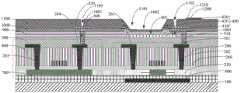
图1为本申请提供的阵列基板的结构剖视图。FIG. 1 is a cross-sectional view of the structure of an array substrate provided by the present application.
图2为本申请所提供的感光传感器以及第一薄膜晶体管在基板上的投影图。FIG. 2 is a projection view of the photosensitive sensor and the first thin film transistor provided by the present application on the substrate.
图3为本申请所提供的阵列基板的制备方法流程图。FIG. 3 is a flow chart of the method for preparing the array substrate provided by the present application.
图4-21为本申请提供的阵列基板的制备方法流程剖视图。4-21 are cross-sectional views of the process flow of the manufacturing method of the array substrate provided in the present application.
具体实施方式Detailed ways
下面将结合本申请实施例中的附图,对本申请实施例中的技术方案进行清楚、完整地描述,显然,所描述的实施例仅仅是本申请一部分实施例,而不是全部的实施例。基于本申请中的实施例,本领域技术人员在没有作出创造性劳动前提下所获得的所有其他实施例,都属于本申请保护的范围。The technical solutions in the embodiments of the present application will be clearly and completely described below with reference to the drawings in the embodiments of the present application. Obviously, the described embodiments are only a part of the embodiments of the present application, but not all of the embodiments. Based on the embodiments in the present application, all other embodiments obtained by those skilled in the art without creative work fall within the protection scope of the present application.
请参阅图1,图1为本申请提供的阵列基板的结构剖视图。本申请提供一种阵列基板10。所述阵列基板10包括基板100、第一薄膜晶体管200、第一层间介质层300、感光传感器400以及第一金属层500。Please refer to FIG. 1 , which is a cross-sectional view of the structure of an array substrate provided by the present application. The present application provides an
所述基板100可以为玻璃基板和柔性基板等。The
在一实施例中,所述阵列基板10还包括遮光层600。所述遮光层600设置于所述基板100上。所述遮光层600的材料包括Mo、Cu、Al和Fe等。所述遮光层用于避免外界光线射入阵列基板中,从而避免阈值电压漂移。In one embodiment, the
在一实施例中,所述阵列基板10还包括缓冲层700。所述缓冲层700覆盖所述基板100以及所述遮光层600。In one embodiment, the
所述第一薄膜晶体管200设置于所述基板100上。所述第一薄膜晶体管200可以为指纹薄膜晶体管开关。具体的,所述第一薄膜晶体管200包括第一有源层210、第一栅极绝缘层220、第一栅极层230、第一源极240、第一漏极250以及第二层间介质层260。所述第一有源层210设置于所述缓冲层700上,并位于所述遮光层600之上。所述第一有源层210包括半导体部211、第一掺杂部212和第二掺杂部213。所述第一掺杂部212设置于所述半导体部211的两侧。所述第二掺杂部213设置于远离所述半导体部211的第一掺杂部212的两侧。所述第一掺杂部212以及所述第二掺杂部213均为N型掺杂。所述第二掺杂部213为N型掺杂,可以使得第一薄膜晶体管易于欧姆接触。所述第一掺杂部212的掺杂浓度大于所述第二掺杂部213的掺杂浓度。所述第一栅极绝缘层220覆盖所述缓冲层700以及所述第一有源层210。所述第一栅极层230设置于所述第一栅极绝缘层220上,并位于所述半导体部211之上。所述第二层间介质层260覆盖所述第一栅极绝缘层220以及所述第一栅极层230。所述第二层间介质层260材料包括SiNx和SiOx中的一种或几种组合。所述第二层间介质层260具有第一过孔261以及第二过孔262。所述第一过孔261贯穿所述第二层间介质层260以及所述第一栅极绝缘层220以暴露所述第二掺杂部213的一侧。所述第二过孔262贯穿所述第二层间介质层260以及所述第一栅极绝缘层220以暴露所述第二掺杂部213的另一侧。所述第一源极240设置于所述第一过孔261中以及所述第二层间介质层260上,并电连接所述第二掺杂部213。所述第一漏极250设置于所述第二过孔262中以及所述第二层间介质层260上,并电连接所述第二掺杂部213。The first
在一实施例中,所述阵列基板10还包括第二薄膜晶体管800。所述第二薄膜晶体管800与所述第一薄膜晶体管200同层设置。所述第二薄膜晶体管800用于驱动显示单元299。具体的,所述第二薄膜晶体管800包括第二有源层810、第一栅极绝缘层220、第二栅极层820、第二源极830和第二漏极840。所述第二有源层810设置于所述缓冲层700上。所述第一薄膜晶体管200与所述第二薄膜晶体管800共用第二栅极绝缘层220。所述第一栅极层820设置于所述第一栅极绝缘层220上,并位于所述第二有源层810之上。所述第二层间介质层260还包括第三过孔263以及第四过孔264。所述第三过孔263贯穿所述第二层间介质层260以及所述栅极绝缘层220以暴露所述第二有源层810的一侧。所述第四过孔264贯穿所述第二层间介质层260以及所述栅极绝缘层220以暴露所述第二有源层810的另一侧。所述第二源极830设置于所述第三过孔263中以及所述第二层间介质层260上,并电连接所述第二有源层810。所述第二漏极840设置于所述第四过孔264中以及所述第二层间介质层260上,并电连接所述第二有源层810。In one embodiment, the
所述第一层间介质层300覆盖所述第一薄膜晶体管200以及所述基板100。所述第一层间介质层300包括第一通孔301。所述第一通孔301贯穿所述第一层间介质层300以暴露所述第一薄膜晶体管层200。具体的,所述第一层间介质层300覆盖所述第一源极240、所述第一漏极250、所述第二源极830、所述第二漏极840以及所述第二层间介质层260。所述第一通孔301贯穿所述第一层间介质层300以暴露所述第一漏极250。The first
所述感光传感器400设置于所述第一层间介质层300上,并位于所述第一薄膜晶体管200之上。所述阵列基板10还包括第二栅极绝缘层900。具体的,所述感光传感器400包括第一掺杂层410、感光层420和第二掺杂层430。所述第一掺杂层410设置于所述第一层间介质层300上。所述第一掺杂层410位于所述第一薄膜晶体管200之上。所述第一掺杂层410为N型掺杂。所述第二栅极绝缘层900设置于所述第一层间介质层300和所述第一掺杂层410上。所述第二栅极绝缘层900具有第五过孔901。所述第五过孔901贯穿所述第二栅极绝缘层900以暴露所述第一掺杂层410。所述感光层420设置于所述第五过孔901中以及所述第二栅极绝缘层900上。所述感光层420的材料为a-Si。所述感光层420的厚度为200纳米-2000纳米。具体的,所述感光层420的厚度可以为300纳米、800纳米、1400纳米、1700纳米或1900纳米。所述第二掺杂层430设置于所述感光层420上。所述第二掺杂层430为P型掺杂。The
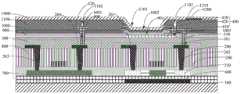
请参阅图2,图2为本申请所提供的感光传感器以及第一薄膜晶体管在基板上的投影图。所述感光传感器400在所述基板100上的投影落在所述第一薄膜晶体管200在所述基板100上的投影之内。Please refer to FIG. 2 . FIG. 2 is a projection view of the photosensitive sensor and the first thin film transistor provided by the present application on the substrate. The projection of the
在本申请中,通过将感光传感器垂直设置于第一薄膜晶体管上,降低了感光传感器的集成对阵列基板的影响;感光层采用a-Si制备,提高了对可见光的吸收,增大了光生电流,并同时通过利用感光传感器和调整感光层的厚度,引入串联电阻,进而降低了感光传感器的暗电流,进而提高感光传感器的灵敏度。In this application, by vertically arranging the photosensitive sensor on the first thin film transistor, the influence of the integration of the photosensitive sensor on the array substrate is reduced; the photosensitive layer is made of a-Si, which improves the absorption of visible light and increases the photogenerated current , and at the same time, by using the photosensitive sensor and adjusting the thickness of the photosensitive layer, a series resistance is introduced, thereby reducing the dark current of the photosensitive sensor, thereby improving the sensitivity of the photosensitive sensor.
在一实施例中,所述阵列基板10还包括第三栅极绝缘层1000。所述第三栅极绝缘层1000覆盖所述第二栅极绝缘层900、所述感光层420以及所述第二掺杂层430上。所述第三栅极绝缘层1000具有第六过孔1001、第七过孔1002和第八过孔1003。所述第六过孔1001贯穿所述第二栅极绝缘层900以及所述第三栅极绝缘层1000以暴露所述第一掺杂层410。所述第七过孔1002贯穿所述第三栅极绝缘层1000以暴露所述第二掺杂层430。所述第八过孔1003贯穿所述第一层间介质层300、所述第二栅极绝缘层900以及所述第三栅极绝缘层1000以暴露所述第二漏极840。所述第一通孔301还贯穿所述第二栅极绝缘层900以及所述第三栅极绝缘层1000以暴露所述第一漏极250。In one embodiment, the
所述第一金属层500设置于所述第一通孔301,并电连接所述第一薄膜晶体管200和所述感光传感器400。具体的,所述第一金属层500包括第一金属部510和第二金属部520。所述第一金属部510设置于所述第一通孔301中、所述第六过孔1001中以及所述第三栅极绝缘层1000上,以电连接所述第一漏极250和第一掺杂层410。所述第二金属部520设置于所述第八过孔1003中以及所述第三栅极绝缘层1000上,并与所述第二漏极840电连接。The
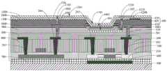
在一实施例中,所述阵列基板10还包括平坦层1100。所述平坦层1100覆盖所述第一层间介质层300、第一金属层500以及所述感光传感器400。所述平坦层1100包括第二通孔1101、第三通孔1102和第五通孔1103。所述第二通孔1101贯穿所述平坦层1100以暴露所述感光传感器400。所述第三通孔1102贯穿所述平坦层1100以暴露所述第一金属层500。所述第五通孔1103贯穿所述平坦层1100以暴露所述第二薄膜晶体管800。具体的,所述平坦层1100覆盖所述第一金属层500以及所述第三栅极绝缘层1000。所述第二通孔1101与所述第七过孔1002贯通以暴露所述第二掺杂层430。所述第五通孔1103贯穿所述平坦层1100以暴露所述第二漏极840。In one embodiment, the
在一实施例中,所述阵列基板10还包括第一存储电容1200、第二存储电容1300、第一钝化层1400、绝缘层1500以及第二钝化层1600。所述第一存储电容1200可以为指纹感光传感器的存储电容。所述第二存储电容1300可以为驱动显示单元的存储电容。具体的,所述第一存储电容1200包括第二金属层1210和第三金属层1220。所述第二金属层1210设置于所述平坦层1100上。所述第一钝化层1400覆盖所述感光传感器400、所述平坦层1100以及所述第二金属层1210。所述平坦层1100的第三通孔1102还贯穿所述第一钝化层1400以暴露所述第一金属层500。所述平坦层1100的第五通孔1103还贯穿所述第一钝化层1400以暴露所述第二漏极840。所述第三金属层1220设置于所述第一钝化层1400上以及所述第三通孔1102中,以电连接所述第一金属部510。所述第二金属层1210与所述第三金属层1220相互绝缘。所述绝缘层1500覆盖所述第一钝化层1400、所述第二金属层1210以及所述第三金属层1220。所述绝缘层1500包括第九过孔1501。所述第九过孔1501贯穿所述绝缘层1500以暴露所述第三金属层1220。所述第二存储电容1300包括第一部分1310和第二部分1320。所述第一部分1310设置于所述第九过孔1501中以及所述绝缘层1500。所述第一部分1310的材料为铟锡氧化物。所述第二钝化层1600覆盖所述绝缘层1500以及所述第一部分1310。所述第二钝化层1600具有第十过孔1601以及所述第十一过孔1602。所述第十过孔1601贯穿所述第一钝化层1400、所述绝缘层1500以及所述第二钝化层1600,并与所述第五通孔1103贯通以暴露所述第二漏极840。所述第十一过孔1602贯穿所述第一钝化层1400、所述绝缘层1500以及所述第二钝化层1600以暴露所述感光传感器400。所述第一钝化层1400包括第四通孔1401。所述第四通孔1401贯穿所述第一钝化层1400、所述绝缘层1500以及所述第二钝化层1600以暴露所述第二金属层1210。所述第二部分1320设置于所述第五通孔1103中以及所述第十过孔1601以电连接所述第二漏极840。所述第一部分1310与所述第二部分1320相互绝缘。In one embodiment, the
在一实施例中,所述阵列基板还包括电极层1700。所述电极层1700设置于所述感光传感器400上、所述第一钝化层1400上、所述第五通孔1103中以及所述第一存储电容1200上。具体的,所述电极层1700设置于所述第四通孔1401中、所述第十一过孔1602以及所述第二钝化层1600,并与所述感光传感器400以及所述第二金属层1210电连接。In one embodiment, the array substrate further includes an
在本申请中,第一薄膜晶体管开关处于打开状态,第一存储电容进行充电,使感光传感器反生反偏,然后第一薄膜晶体管关闭,当入射光入射到感光传感器,使第一存储电容的电荷量降低,通过监控电荷量的改变,得到指纹谷和脊特征信号,进而完成指纹识别。In the present application, the switch of the first thin film transistor is in the open state, the first storage capacitor is charged, and the photosensitive sensor is reversely biased, and then the first thin film transistor is turned off. When the incident light enters the photosensitive sensor, the first storage capacitor is charged. When the charge amount is reduced, the fingerprint valley and ridge characteristic signals are obtained by monitoring the change of the charge amount, and then the fingerprint identification is completed.
请参阅图3和图4-21,图3为本申请所提供的阵列基板的制备方法流程图。图4-21为本申请提供的阵列基板的制备方法流程剖视图。本申请还提供一种阵列基板的制备方法。所述制备方法包括:Please refer to FIG. 3 and FIGS. 4-21 . FIG. 3 is a flow chart of the method for fabricating the array substrate provided in the present application. 4-21 are cross-sectional views of the process flow of the manufacturing method of the array substrate provided in the present application. The present application also provides a preparation method of the array substrate. The preparation method includes:
20、提供一基板100。20. A
请参阅图4和图5。在提供一基板100的步骤之后,还包括:See Figure 4 and Figure 5. After the step of providing a
在所述基板100上设置遮光层600材料,蚀刻曝光形成遮光层600。所述遮光层600的材料包括Mo、Cu、Al和Fe等。所述遮光层用于避免外界光线射入阵列基板中,从而避免阈值电压漂移。The material of the
在所述基板100上设置遮光层600的步骤之后,还包括:After the step of disposing the
在所述基板100以及所述遮光层600上形成缓冲层700。A
30、在所述基板100上设置第一薄膜晶体管200。30. Disposing a first
请参阅图5-图8。具体的,在所述缓冲层700上设置第一有源层210的材料以及所述第二有源层810材料,采用蚀刻曝光方法形成第一有源层210和第二有源层810。然后,对所述有源层210进行磷离子掺杂、砷离子掺杂或锑离子掺杂等,以形成N+型掺杂个第二掺杂部213,可以使得第一薄膜晶体管易于欧姆接触。所述第一有源层210位于所述遮光层600之上。所述第一有源层210材料和所述第二有源层810材料为多晶硅。所述第一有源层210与所述第二有源层810不相连。然后,在所述缓冲层700、所述第一有源层210以及所述第二有源层810上沉积第一栅极绝缘层220。然后,在所述第一栅极绝缘层220上设置第一栅极层230材料以及第二栅极层820材料,蚀刻形成第一栅极层230以及第二栅极层820,所述第一栅极层230位于所述第一有源层210之上。所述第二栅极层820位于所述第二有源层810之上。所述第一栅极层230与所述第二栅极层820相互绝缘。然后,以所述第一栅极层230为遮挡,对所述第一有源层210进行N-离子注入,形成第一掺杂部212。所述第一掺杂部212设置于所述半导体部211的两侧。所述第二掺杂部213设置于远离所述半导体部211的第一掺杂部212的两侧。所述第一掺杂部212为N-型掺杂。所述第一掺杂部212的掺杂浓度小于所述第二掺杂部213的浓度。然后,在所述第一栅极绝缘层220、所述第一栅极层230以及所述第二栅极层820上沉积第二层间介质层260材料,对所述第一层间介质层260材料采用快速热退火进行氢化和活化,并进行曝光蚀刻,形成第一层间介质层260。所述第二层间介质层260材料包括SiNx和SiOx中的一种或几种组合。所述第二层间介质层260具有第一过孔261、第二过孔262、第三过孔263以及第四过孔264。所述第一过孔261贯穿所述第二层间介质层260以及所述第一栅极绝缘层220以暴露所述第二掺杂部213的一侧。所述第二过孔262贯穿所述第二层间介质层260以及所述第一栅极绝缘层220以暴露所述第二掺杂部213的另一侧。所述第三过孔263贯穿所述第二层间介质层260以及所述栅极绝缘层220以暴露所述第二有源层810的一侧。所述第四过孔264贯穿所述第二层间介质层260以及所述栅极绝缘层220以暴露所述第二有源层810的另一侧。然后,在所述第一过孔261中、所述第二过孔262、所述第三过孔263、所述第四过孔264以及所述第二层间介质层260上设置源漏极材料,对所述源漏极材料进行蚀刻曝光,形成第一源极240、第一漏极250、第二源极830以及第二漏极840。所述第一源极240、所述第一漏极250、所述第二源极830以及所述第二漏极840之间相互绝缘。所述第一源极240位于所述第一过孔261中以及所述第二层间介质层260上,并电连接所述第二掺杂部213。所述第一漏极250位于所述第二过孔262中以及所述第二层间介质层260上,并电连接所述第二掺杂部213。所述第二源极830位于所述第三过孔263中以及所述第二层间介质层260上,并电连接所述第二有源层810。所述第二漏极840位于所述第四过孔264中以及所述第二层间介质层260上,并电连接所述第二有源层810。所述第一有源层210、所述第一栅极绝缘层220、所述第一栅极层230、所述第一源极240、所述第一漏极250以及所述第二层间介质层260形成第一薄膜晶体管200。所述第一薄膜晶体管200可以为指纹薄膜晶体管开关。所述第二有源层810、所述第一栅极绝缘层220、所述第二栅极层820、所述第二源极830和所述第二漏极840形成第二薄膜晶体管800。所述第二薄膜晶体管800用于驱动显示单元299。See Figures 5-8. Specifically, the material of the first
40、在所述基板100以及所述第一薄膜晶体管200上设置第一层间介质层300,所述第一层间介质层300包括第一通孔301,所述第一通孔301贯穿所述第一层间介质层300以暴露所述第一薄膜晶体管200。40. A first
请参阅图9。具体的,在所述第二层间介质层260、所述第一源极240、所述第一漏极250、所述第二源极830以及所述第二漏极840上设置第一层间介质层材料,形成第一层间介质层300。See Figure 9. Specifically, a first layer is provided on the second
50、在所述第一层间介质层300上设置感光传感器400,并位于所述第一薄膜晶体管200之上。50. Disposing a
请参阅图9-图12。具体的,在所述第一层间介质层300上沉积第一掺杂层410材料,蚀刻形成第一掺杂层410。所述第一掺杂层410位于所述第一薄膜晶体管200之上。所述第一掺杂层410为N型掺杂。然后,在所述第一掺杂层410上依次层叠沉积感光层420的材料以及第二掺杂层430材料,蚀刻形成感光层420以及第二掺杂层430。所述感光层420的材料为a-Si。所述感光层420的厚度为200纳米-2000纳米。具体的,所述感光层420的厚度可以为300纳米、800纳米、1400纳米、1700纳米或1900纳米。所述第二掺杂层430设置于所述感光层420上。所述第二掺杂层430为P型掺杂。所述第一掺杂层410、所述感光层420以及所述第二掺杂层430形成感光传感器400。See Figures 9-12. Specifically, the material of the first doped
在所述第一层间介质层300上设置第一掺杂层410的步骤之后,在所述第一掺杂层410上依次层叠设置感光层420以及第二掺杂层430的步骤之前,还包括:After the step of arranging the first doped
在所述第一层间介质层300以及所述第一掺杂层410上沉积第二栅极绝缘层900材料,对所述第一栅极绝缘层900材料采用快速热退火进行氢化和活化,并进行曝光蚀刻形成第一栅极绝缘层900。所述第二栅极绝缘层900具有第五过孔901。所述第五过孔901贯穿所述第二栅极绝缘层900以暴露所述一掺杂层410。所述感光层420以及所述第二掺杂层430设置于所述第二过孔中以及所述第二栅极绝缘层900上。A second
在所述第一层间介质层300以及所述第一掺杂层410上设置第二栅极绝缘层900的步骤之后,还包括:After the step of disposing the second
在所述第二栅极绝缘层900、所述感光层420以及所述第二掺杂层430上沉积第三栅极绝缘层1000材料,蚀刻形成第三栅极绝缘层1000。所述第三栅极绝缘层1000具有第六过孔1001、第七过孔1002和第八过孔1003。所述第六过孔1001贯穿所述第二栅极绝缘层900以及所述第三栅极绝缘层1000以暴露所述第一掺杂层410。所述第七过孔1002贯穿所述第三栅极绝缘层1000以暴露所述第二掺杂层430。所述第八过孔1003贯穿所述第一层间介质层300、所述第二栅极绝缘层900以及所述第三栅极绝缘层1000以暴露所述第二漏极840。形成所述第六过孔1001、所述第七过孔1002和所述第八过孔1003的同时,形成第一通孔301。第一通孔301为所述第一层间介质层300的第一通孔301。所述第一通孔301贯穿所述第一层间介质层300、所述第二栅极绝缘层900以及所述第三栅极绝缘层1000以暴露所述第一漏极250。A third
60、在所述第一通孔301中以及所述第一层间介质层300上设置第一金属层400,并电连接所述第一薄膜晶体管200和所述感光传感器400。60. A
请参阅图13-图21。具体的,在所述第二掺杂层430、所述第三栅极绝缘层1000上沉积第一金属层500材料,蚀刻形成第一金属层500。所述第一金属层500包括第一金属部510和第二金属部520。所述第一金属部510设置于所述第一通孔301中、所述第六过孔1001中以及所述第三栅极绝缘层1000上,以电连接所述第一漏极250和第一掺杂层410。所述第二金属部520设置于所述第八过孔1003中以及所述第三栅极绝缘层1000上,并与所述第二漏极840电连接。See Figures 13-21. Specifically, the material of the
在所述第一通孔301中以及所述第一层间介质层300上设置第一金属层500,并电连接所述第一薄膜晶体管200和所述感光传感器400的步骤之后,还包括:After the step of disposing a
在所述第二掺杂层430、所述第三栅极绝缘层1000以及所述第一金属层500上设置平坦层1100材料,蚀刻形成具有第二通孔1101和第三通孔1102的平坦层1100。所述第二通孔1101贯穿所述平坦层1100,并与所述第七过孔1002贯通以暴露所述第二掺杂层430。所述第三通孔1102贯穿所述平坦层1100以暴露所述第一金属层500。The material of the
在所述第二掺杂层430、所述第三栅极绝缘层1000以及所述第一金属层500上设置平坦层1100的步骤之后,还包括:After the step of disposing the
在所述第二掺杂层430、所述第一金属层500以及所述平坦层1100上沉积第二金属层1210材料,蚀刻形成第二金属层1210。The material of the
在所述第二掺杂层430、所述第一金属层500以及所述平坦层1100上设置第二金属层1210的步骤之后,还包括:After the step of disposing the
在所述第二掺杂层430、所述平坦层1100以及第二金属层1210上设置第一钝化层1400材料,蚀刻形成第一钝化层1400。形成第一钝化层1400的同时,形成所述平坦层的第五通孔1103。所述第五通孔1103贯穿所述平坦层1100以暴露所述第二漏极840。A
在所述第二掺杂层430、所述平坦层1100以及第二金属层1210上设置第一钝化层1400的步骤的之后,还包括:After the step of disposing the
在所述第一钝化层1400以及所述第三通孔1102沉积第三金属层1220材料,蚀刻形成第三金属层1220。A
在所述第一钝化层1400以及所述第三通孔1102形成第三金属层1220的步骤之后,还包括:After the step of forming the
在所述第一钝化层1400以及所述第三金属层1220上沉积绝缘层1500材料,蚀刻形成绝缘层1500。所述绝缘层1500包括第九过孔1501。所述第九过孔1501贯穿所述绝缘层1500以暴露所述第三金属层1200。An insulating
在所述第一钝化层1400以及所述第三金属层1220上形成绝缘层1500的步骤之后,还包括:After the step of forming the insulating
在所述第九过孔1501以及所述绝缘层1500上沉积第一部分1310材料,蚀刻形成第二存储电容1300的第一部分1310。所述第一部分1310的材料为铟锡氧化物。A
在所述第九过孔1501以及所述绝缘层1500上形成第一部分1310的步骤之后,还包括:After the step of forming the
在所述绝缘层1500以及所述第一部分1310上沉积第二钝化层1600材料,蚀刻形成第二钝化层1600。所述第二钝化层1600具有第十过孔1601以及所述第十一过孔1602。所述第十过孔1601贯穿所述第一钝化层1400、所述绝缘层1500以及所述第二钝化层1600,并与所述第五通孔1103贯通以暴露所述第二漏极840。所述第十一过孔1602贯穿所述第一钝化层1400、所述绝缘层1500以及所述第二钝化层1600以暴露所述感光传感器400。所述第一钝化层1400包括第四通孔1401。所述第四通孔1401贯穿所述第一钝化层1400、所述绝缘层1500以及所述第二钝化层1600以暴露所述第二金属层1210。A
在所述绝缘层1500以及所述第一部分1310上形成第二钝化层1600的步骤之后,还包括:After the step of forming the
在所述第二钝化层1600上、所述第五通孔1103中、所述第十过孔1601、所述第十一过孔1602以及所述第四通孔1401中沉积第二部分1320材料以及所述电极层1700材料,蚀刻形成第二部分1320以及所述电极层1700。所述第二部分1320通过所述第五通孔1103以及所述第十过孔1601与所述第二漏极840电连接。所述第一部分1310与所述第二部分1320相互绝缘。所述第一部分1310与所述第二部分1320组成第二存储电容1300。所述第二存储电容1300可以为驱动显示单元的存储电容。所述电极层1700通过所述第四通孔1401与所述第二金属层1210电连接,并通所述第十一过孔1602与所述第二掺杂层430电连接。A
在本申请中,通过采用与阵列基板兼容的低温多晶硅产线离子植入和快速退火工艺来进行制备,可以降低感光传感器的集成对阵列基板的开口率的影响。In the present application, by adopting a low-temperature polysilicon production line ion implantation and rapid annealing process compatible with the array substrate, the influence of the integration of the photosensors on the aperture ratio of the array substrate can be reduced.
本申请提供一种阵列基板及其制备方法,所述阵列基板包括基板、第一薄膜晶体管、第一层间介质层、感光传感器以及第一金属层,所述第一薄膜晶体管设置于所述基板上,所述第一层间介质层覆盖所述第一薄膜晶体管以及所述基板,所述第一层间介质层包括第一通孔,所述第一通孔贯穿所述第一层间介质层以暴露所述第一薄膜晶体管层,所述感光传感器设置于所述第一层间介质层上,并位于所述第一薄膜晶体管之上,所述第一金属层设置于所述第一通孔,并电连接所述第一薄膜晶体管和所述感光传感器。通过将感光传感器设置于第一薄膜晶体管上,提高了阵列基板的开口率;感光层采用a-Si材料进行制备,增强感光二极管对可见光的吸收,增大光生电流,同时利用感光传感器和调整感光层的厚度,降低感光传感器的暗电流,进而提高感光传感器的灵敏度。The present application provides an array substrate and a preparation method thereof. The array substrate includes a substrate, a first thin film transistor, a first interlayer dielectric layer, a photosensitive sensor and a first metal layer, and the first thin film transistor is disposed on the substrate above, the first interlayer dielectric layer covers the first thin film transistor and the substrate, the first interlayer dielectric layer includes a first through hole, and the first through hole penetrates the first interlayer dielectric layer to expose the first thin film transistor layer, the photosensitive sensor is disposed on the first interlayer dielectric layer and above the first thin film transistor, and the first metal layer is disposed on the first A through hole is used to electrically connect the first thin film transistor and the photosensitive sensor. By arranging the photosensitive sensor on the first thin film transistor, the aperture ratio of the array substrate is improved; the photosensitive layer is made of a-Si material, which enhances the absorption of visible light by the photosensitive diode and increases the photo-generated current. The thickness of the layer reduces the dark current of the photosensitive sensor, thereby improving the sensitivity of the photosensitive sensor.
以上对本申请实施方式提供了详细介绍,本文中应用了具体个例对本申请的原理及实施方式进行了阐述,以上实施方式的说明只是用于帮助理解本申请。同时,对于本领域的技术人员,依据本申请的思想,在具体实施方式及应用范围上均会有改变之处,综上所述,本说明书内容不应理解为对本申请的限制。The above provides a detailed introduction to the embodiments of the present application. Specific examples are used herein to illustrate the principles and implementations of the present application. The descriptions of the above embodiments are only used to help understand the present application. At the same time, for those skilled in the art, according to the idea of the present application, there will be changes in the specific embodiments and application scope. To sum up, the content of this specification should not be construed as a limitation to the present application.
Claims (10)
Translated fromChinesePriority Applications (1)
| Application Number | Priority Date | Filing Date | Title |
|---|---|---|---|
| CN202010787785.7ACN111968994B (en) | 2020-08-07 | 2020-08-07 | Array substrate and preparation method thereof |
Applications Claiming Priority (1)
| Application Number | Priority Date | Filing Date | Title |
|---|---|---|---|
| CN202010787785.7ACN111968994B (en) | 2020-08-07 | 2020-08-07 | Array substrate and preparation method thereof |
Publications (2)
| Publication Number | Publication Date |
|---|---|
| CN111968994Atrue CN111968994A (en) | 2020-11-20 |
| CN111968994B CN111968994B (en) | 2024-03-05 |
Family
ID=73364823
Family Applications (1)
| Application Number | Title | Priority Date | Filing Date |
|---|---|---|---|
| CN202010787785.7AActiveCN111968994B (en) | 2020-08-07 | 2020-08-07 | Array substrate and preparation method thereof |
Country Status (1)
| Country | Link |
|---|---|
| CN (1) | CN111968994B (en) |
Cited By (4)
| Publication number | Priority date | Publication date | Assignee | Title |
|---|---|---|---|---|
| CN112582438A (en)* | 2020-12-10 | 2021-03-30 | 武汉华星光电技术有限公司 | Display panel and preparation method thereof |
| CN114188358A (en)* | 2021-12-08 | 2022-03-15 | 武汉华星光电技术有限公司 | A kind of display panel and display panel manufacturing method |
| CN115016173A (en)* | 2022-06-07 | 2022-09-06 | 武汉华星光电技术有限公司 | Backlight module and display device |
| WO2022257205A1 (en)* | 2021-06-07 | 2022-12-15 | 武汉华星光电技术有限公司 | Array substrate, manufacturing method for array substrate, and display apparatus |
Citations (7)
| Publication number | Priority date | Publication date | Assignee | Title |
|---|---|---|---|---|
| JP2003158253A (en)* | 2002-07-17 | 2003-05-30 | Canon Inc | Photoelectric conversion device and X-ray detection device using the same |
| US20170047449A1 (en)* | 2015-08-10 | 2017-02-16 | Nlt Technologies, Ltd. | Optical sensor element and photoelectric conversion device |
| CN108258024A (en)* | 2018-01-29 | 2018-07-06 | 上海天马微电子有限公司 | Display panel and display device |
| CN108878503A (en)* | 2018-07-26 | 2018-11-23 | 京东方科技集团股份有限公司 | Oled display substrate and its manufacturing method, OLED display panel, display device |
| CN109728050A (en)* | 2019-01-02 | 2019-05-07 | 京东方科技集团股份有限公司 | Array substrate and preparation method thereof, display panel and display device |
| CN110458036A (en)* | 2019-07-17 | 2019-11-15 | 武汉华星光电技术有限公司 | Fingerprint recognition mould group and preparation method thereof, relevant apparatus |
| CN110690227A (en)* | 2019-09-05 | 2020-01-14 | 武汉华星光电技术有限公司 | Array substrate, manufacturing method thereof, and display device |
- 2020
- 2020-08-07CNCN202010787785.7Apatent/CN111968994B/enactiveActive
Patent Citations (7)
| Publication number | Priority date | Publication date | Assignee | Title |
|---|---|---|---|---|
| JP2003158253A (en)* | 2002-07-17 | 2003-05-30 | Canon Inc | Photoelectric conversion device and X-ray detection device using the same |
| US20170047449A1 (en)* | 2015-08-10 | 2017-02-16 | Nlt Technologies, Ltd. | Optical sensor element and photoelectric conversion device |
| CN108258024A (en)* | 2018-01-29 | 2018-07-06 | 上海天马微电子有限公司 | Display panel and display device |
| CN108878503A (en)* | 2018-07-26 | 2018-11-23 | 京东方科技集团股份有限公司 | Oled display substrate and its manufacturing method, OLED display panel, display device |
| CN109728050A (en)* | 2019-01-02 | 2019-05-07 | 京东方科技集团股份有限公司 | Array substrate and preparation method thereof, display panel and display device |
| CN110458036A (en)* | 2019-07-17 | 2019-11-15 | 武汉华星光电技术有限公司 | Fingerprint recognition mould group and preparation method thereof, relevant apparatus |
| CN110690227A (en)* | 2019-09-05 | 2020-01-14 | 武汉华星光电技术有限公司 | Array substrate, manufacturing method thereof, and display device |
Cited By (8)
| Publication number | Priority date | Publication date | Assignee | Title |
|---|---|---|---|---|
| CN112582438A (en)* | 2020-12-10 | 2021-03-30 | 武汉华星光电技术有限公司 | Display panel and preparation method thereof |
| CN112582438B (en)* | 2020-12-10 | 2022-05-31 | 武汉华星光电技术有限公司 | Display panel and method of making the same |
| WO2022257205A1 (en)* | 2021-06-07 | 2022-12-15 | 武汉华星光电技术有限公司 | Array substrate, manufacturing method for array substrate, and display apparatus |
| US11847850B2 (en) | 2021-06-07 | 2023-12-19 | Wuhan China Star Optoelectronics Technology Co., Ltd. | Array substrate, manufacturing method thereof, and display device |
| CN114188358A (en)* | 2021-12-08 | 2022-03-15 | 武汉华星光电技术有限公司 | A kind of display panel and display panel manufacturing method |
| CN115016173A (en)* | 2022-06-07 | 2022-09-06 | 武汉华星光电技术有限公司 | Backlight module and display device |
| CN115016173B (en)* | 2022-06-07 | 2023-12-15 | 武汉华星光电技术有限公司 | Backlight module and display device |
| US12265298B2 (en) | 2022-06-07 | 2025-04-01 | Wuhan China Star Optoelectronics Technology Co., Ltd. | Backlight module and display device |
Also Published As
| Publication number | Publication date |
|---|---|
| CN111968994B (en) | 2024-03-05 |
Similar Documents
| Publication | Publication Date | Title |
|---|---|---|
| CN111968994B (en) | Array substrate and preparation method thereof | |
| CN110729309B (en) | Display panel, preparation method thereof and display device | |
| US8198149B2 (en) | Method for fabricating active device array substrate | |
| US20090278121A1 (en) | System for displaying images and fabrication method thereof | |
| CN112928134B (en) | Array substrates and display panels | |
| CN106486499B (en) | A circuit structure and manufacturing method and display panel | |
| US20150129865A1 (en) | Semiconductor device and method for manufacturing same | |
| CN110265509B (en) | Photoelectric detection device, preparation method thereof, display panel and display device | |
| US10615188B2 (en) | Array substrate and manufacturing method thereof | |
| CN109427836B (en) | Array substrate, X-ray detector, and method for manufacturing the same | |
| WO2015141777A1 (en) | Light detection device | |
| US20210083137A1 (en) | Optoelectronic Sensor and Manufacturing Method Thereof, and Optoelectronic Device and Manufacturing Method Thereof | |
| CN105453269B (en) | Radioscopic image sensor substrate | |
| CN112259556A (en) | Array substrate and preparation method thereof | |
| WO2014173078A1 (en) | Thin film transistor, method for manufactur thereof and array substrate | |
| GB2548759A (en) | Array substrate, display panel, and manufacturing method for array substrate | |
| KR100850289B1 (en) | Image sensor of laminated structure and manufacturing method | |
| CN120500117A (en) | Solar cell and photovoltaic module | |
| US11735611B2 (en) | Drive backplane, manufacturing method thereof, detection substrate, and detection device | |
| CN104900712A (en) | TFT substrate structure manufacturing method and TFT substrate structure thereof | |
| CN113571533A (en) | Array substrate and display panel | |
| CN112242407B (en) | Array substrate and preparation method thereof | |
| KR20150089299A (en) | A Display device, method of fabricating the same, and method of fabricating an image sensor device | |
| WO2020062415A1 (en) | Display panel and manufacturing method therefor | |
| CN207517701U (en) | A kind of thin film transistor and display panel |
Legal Events
| Date | Code | Title | Description |
|---|---|---|---|
| PB01 | Publication | ||
| PB01 | Publication | ||
| SE01 | Entry into force of request for substantive examination | ||
| SE01 | Entry into force of request for substantive examination | ||
| GR01 | Patent grant | ||
| GR01 | Patent grant |