CN111952256B - electronic packaging - Google Patents
electronic packagingDownload PDFInfo
- Publication number
- CN111952256B CN111952256BCN202010332486.4ACN202010332486ACN111952256BCN 111952256 BCN111952256 BCN 111952256BCN 202010332486 ACN202010332486 ACN 202010332486ACN 111952256 BCN111952256 BCN 111952256B
- Authority
- CN
- China
- Prior art keywords
- package
- package substrate
- top surface
- interface circuit
- speed interface
- Prior art date
- Legal status (The legal status is an assumption and is not a legal conclusion. Google has not performed a legal analysis and makes no representation as to the accuracy of the status listed.)
- Active
Links
Images


Classifications
- H—ELECTRICITY
- H01—ELECTRIC ELEMENTS
- H01L—SEMICONDUCTOR DEVICES NOT COVERED BY CLASS H10
- H01L23/00—Details of semiconductor or other solid state devices
- H01L23/28—Encapsulations, e.g. encapsulating layers, coatings, e.g. for protection
- H01L23/31—Encapsulations, e.g. encapsulating layers, coatings, e.g. for protection characterised by the arrangement or shape
- H01L23/3107—Encapsulations, e.g. encapsulating layers, coatings, e.g. for protection characterised by the arrangement or shape the device being completely enclosed
- H01L23/3121—Encapsulations, e.g. encapsulating layers, coatings, e.g. for protection characterised by the arrangement or shape the device being completely enclosed a substrate forming part of the encapsulation
- H01L23/3128—Encapsulations, e.g. encapsulating layers, coatings, e.g. for protection characterised by the arrangement or shape the device being completely enclosed a substrate forming part of the encapsulation the substrate having spherical bumps for external connection
- H—ELECTRICITY
- H01—ELECTRIC ELEMENTS
- H01L—SEMICONDUCTOR DEVICES NOT COVERED BY CLASS H10
- H01L23/00—Details of semiconductor or other solid state devices
- H01L23/52—Arrangements for conducting electric current within the device in operation from one component to another, i.e. interconnections, e.g. wires, lead frames
- H01L23/538—Arrangements for conducting electric current within the device in operation from one component to another, i.e. interconnections, e.g. wires, lead frames the interconnection structure between a plurality of semiconductor chips being formed on, or in, insulating substrates
- H01L23/5386—Geometry or layout of the interconnection structure
- H—ELECTRICITY
- H01—ELECTRIC ELEMENTS
- H01L—SEMICONDUCTOR DEVICES NOT COVERED BY CLASS H10
- H01L25/00—Assemblies consisting of a plurality of semiconductor or other solid state devices
- H01L25/16—Assemblies consisting of a plurality of semiconductor or other solid state devices the devices being of types provided for in two or more different subclasses of H10B, H10D, H10F, H10H, H10K or H10N, e.g. forming hybrid circuits
- H—ELECTRICITY
- H01—ELECTRIC ELEMENTS
- H01L—SEMICONDUCTOR DEVICES NOT COVERED BY CLASS H10
- H01L23/00—Details of semiconductor or other solid state devices
- H01L23/34—Arrangements for cooling, heating, ventilating or temperature compensation ; Temperature sensing arrangements
- H01L23/36—Selection of materials, or shaping, to facilitate cooling or heating, e.g. heatsinks
- H01L23/367—Cooling facilitated by shape of device
- H01L23/3675—Cooling facilitated by shape of device characterised by the shape of the housing
- H—ELECTRICITY
- H01—ELECTRIC ELEMENTS
- H01L—SEMICONDUCTOR DEVICES NOT COVERED BY CLASS H10
- H01L23/00—Details of semiconductor or other solid state devices
- H01L23/58—Structural electrical arrangements for semiconductor devices not otherwise provided for, e.g. in combination with batteries
- H01L23/585—Structural electrical arrangements for semiconductor devices not otherwise provided for, e.g. in combination with batteries comprising conductive layers or plates or strips or rods or rings
- H—ELECTRICITY
- H01—ELECTRIC ELEMENTS
- H01L—SEMICONDUCTOR DEVICES NOT COVERED BY CLASS H10
- H01L23/00—Details of semiconductor or other solid state devices
- H01L23/58—Structural electrical arrangements for semiconductor devices not otherwise provided for, e.g. in combination with batteries
- H01L23/64—Impedance arrangements
- H01L23/66—High-frequency adaptations
- H—ELECTRICITY
- H01—ELECTRIC ELEMENTS
- H01L—SEMICONDUCTOR DEVICES NOT COVERED BY CLASS H10
- H01L24/00—Arrangements for connecting or disconnecting semiconductor or solid-state bodies; Methods or apparatus related thereto
- H01L24/01—Means for bonding being attached to, or being formed on, the surface to be connected, e.g. chip-to-package, die-attach, "first-level" interconnects; Manufacturing methods related thereto
- H01L24/02—Bonding areas ; Manufacturing methods related thereto
- H—ELECTRICITY
- H01—ELECTRIC ELEMENTS
- H01L—SEMICONDUCTOR DEVICES NOT COVERED BY CLASS H10
- H01L24/00—Arrangements for connecting or disconnecting semiconductor or solid-state bodies; Methods or apparatus related thereto
- H01L24/01—Means for bonding being attached to, or being formed on, the surface to be connected, e.g. chip-to-package, die-attach, "first-level" interconnects; Manufacturing methods related thereto
- H01L24/10—Bump connectors ; Manufacturing methods related thereto
- H01L24/12—Structure, shape, material or disposition of the bump connectors prior to the connecting process
- H01L24/13—Structure, shape, material or disposition of the bump connectors prior to the connecting process of an individual bump connector
- H—ELECTRICITY
- H01—ELECTRIC ELEMENTS
- H01L—SEMICONDUCTOR DEVICES NOT COVERED BY CLASS H10
- H01L24/00—Arrangements for connecting or disconnecting semiconductor or solid-state bodies; Methods or apparatus related thereto
- H01L24/01—Means for bonding being attached to, or being formed on, the surface to be connected, e.g. chip-to-package, die-attach, "first-level" interconnects; Manufacturing methods related thereto
- H01L24/18—High density interconnect [HDI] connectors; Manufacturing methods related thereto
- H01L24/20—Structure, shape, material or disposition of high density interconnect preforms
- H—ELECTRICITY
- H01—ELECTRIC ELEMENTS
- H01L—SEMICONDUCTOR DEVICES NOT COVERED BY CLASS H10
- H01L2223/00—Details relating to semiconductor or other solid state devices covered by the group H01L23/00
- H01L2223/58—Structural electrical arrangements for semiconductor devices not otherwise provided for
- H01L2223/64—Impedance arrangements
- H01L2223/66—High-frequency adaptations
- H01L2223/6605—High-frequency electrical connections
- H01L2223/6638—Differential pair signal lines
- H—ELECTRICITY
- H01—ELECTRIC ELEMENTS
- H01L—SEMICONDUCTOR DEVICES NOT COVERED BY CLASS H10
- H01L2223/00—Details relating to semiconductor or other solid state devices covered by the group H01L23/00
- H01L2223/58—Structural electrical arrangements for semiconductor devices not otherwise provided for
- H01L2223/64—Impedance arrangements
- H01L2223/66—High-frequency adaptations
- H01L2223/6661—High-frequency adaptations for passive devices
- H01L2223/6666—High-frequency adaptations for passive devices for decoupling, e.g. bypass capacitors
- H—ELECTRICITY
- H01—ELECTRIC ELEMENTS
- H01L—SEMICONDUCTOR DEVICES NOT COVERED BY CLASS H10
- H01L2224/00—Indexing scheme for arrangements for connecting or disconnecting semiconductor or solid-state bodies and methods related thereto as covered by H01L24/00
- H01L2224/01—Means for bonding being attached to, or being formed on, the surface to be connected, e.g. chip-to-package, die-attach, "first-level" interconnects; Manufacturing methods related thereto
- H01L2224/02—Bonding areas; Manufacturing methods related thereto
- H01L2224/023—Redistribution layers [RDL] for bonding areas
- H01L2224/0233—Structure of the redistribution layers
- H01L2224/02333—Structure of the redistribution layers being a bump
- H—ELECTRICITY
- H01—ELECTRIC ELEMENTS
- H01L—SEMICONDUCTOR DEVICES NOT COVERED BY CLASS H10
- H01L2224/00—Indexing scheme for arrangements for connecting or disconnecting semiconductor or solid-state bodies and methods related thereto as covered by H01L24/00
- H01L2224/01—Means for bonding being attached to, or being formed on, the surface to be connected, e.g. chip-to-package, die-attach, "first-level" interconnects; Manufacturing methods related thereto
- H01L2224/02—Bonding areas; Manufacturing methods related thereto
- H01L2224/04—Structure, shape, material or disposition of the bonding areas prior to the connecting process
- H01L2224/04105—Bonding areas formed on an encapsulation of the semiconductor or solid-state body, e.g. bonding areas on chip-scale packages
- H—ELECTRICITY
- H01—ELECTRIC ELEMENTS
- H01L—SEMICONDUCTOR DEVICES NOT COVERED BY CLASS H10
- H01L2224/00—Indexing scheme for arrangements for connecting or disconnecting semiconductor or solid-state bodies and methods related thereto as covered by H01L24/00
- H01L2224/01—Means for bonding being attached to, or being formed on, the surface to be connected, e.g. chip-to-package, die-attach, "first-level" interconnects; Manufacturing methods related thereto
- H01L2224/10—Bump connectors; Manufacturing methods related thereto
- H01L2224/12—Structure, shape, material or disposition of the bump connectors prior to the connecting process
- H01L2224/12105—Bump connectors formed on an encapsulation of the semiconductor or solid-state body, e.g. bumps on chip-scale packages
- H—ELECTRICITY
- H01—ELECTRIC ELEMENTS
- H01L—SEMICONDUCTOR DEVICES NOT COVERED BY CLASS H10
- H01L2224/00—Indexing scheme for arrangements for connecting or disconnecting semiconductor or solid-state bodies and methods related thereto as covered by H01L24/00
- H01L2224/01—Means for bonding being attached to, or being formed on, the surface to be connected, e.g. chip-to-package, die-attach, "first-level" interconnects; Manufacturing methods related thereto
- H01L2224/10—Bump connectors; Manufacturing methods related thereto
- H01L2224/12—Structure, shape, material or disposition of the bump connectors prior to the connecting process
- H01L2224/13—Structure, shape, material or disposition of the bump connectors prior to the connecting process of an individual bump connector
- H01L2224/13001—Core members of the bump connector
- H01L2224/13005—Structure
- H01L2224/13008—Bump connector integrally formed with a redistribution layer on the semiconductor or solid-state body
- H—ELECTRICITY
- H01—ELECTRIC ELEMENTS
- H01L—SEMICONDUCTOR DEVICES NOT COVERED BY CLASS H10
- H01L2224/00—Indexing scheme for arrangements for connecting or disconnecting semiconductor or solid-state bodies and methods related thereto as covered by H01L24/00
- H01L2224/01—Means for bonding being attached to, or being formed on, the surface to be connected, e.g. chip-to-package, die-attach, "first-level" interconnects; Manufacturing methods related thereto
- H01L2224/10—Bump connectors; Manufacturing methods related thereto
- H01L2224/15—Structure, shape, material or disposition of the bump connectors after the connecting process
- H01L2224/16—Structure, shape, material or disposition of the bump connectors after the connecting process of an individual bump connector
- H01L2224/161—Disposition
- H01L2224/16151—Disposition the bump connector connecting between a semiconductor or solid-state body and an item not being a semiconductor or solid-state body, e.g. chip-to-substrate, chip-to-passive
- H01L2224/16221—Disposition the bump connector connecting between a semiconductor or solid-state body and an item not being a semiconductor or solid-state body, e.g. chip-to-substrate, chip-to-passive the body and the item being stacked
- H01L2224/16225—Disposition the bump connector connecting between a semiconductor or solid-state body and an item not being a semiconductor or solid-state body, e.g. chip-to-substrate, chip-to-passive the body and the item being stacked the item being non-metallic, e.g. insulating substrate with or without metallisation
- H01L2224/16227—Disposition the bump connector connecting between a semiconductor or solid-state body and an item not being a semiconductor or solid-state body, e.g. chip-to-substrate, chip-to-passive the body and the item being stacked the item being non-metallic, e.g. insulating substrate with or without metallisation the bump connector connecting to a bond pad of the item
- H—ELECTRICITY
- H01—ELECTRIC ELEMENTS
- H01L—SEMICONDUCTOR DEVICES NOT COVERED BY CLASS H10
- H01L2224/00—Indexing scheme for arrangements for connecting or disconnecting semiconductor or solid-state bodies and methods related thereto as covered by H01L24/00
- H01L2224/01—Means for bonding being attached to, or being formed on, the surface to be connected, e.g. chip-to-package, die-attach, "first-level" interconnects; Manufacturing methods related thereto
- H01L2224/18—High density interconnect [HDI] connectors; Manufacturing methods related thereto
- H01L2224/23—Structure, shape, material or disposition of the high density interconnect connectors after the connecting process
- H01L2224/24—Structure, shape, material or disposition of the high density interconnect connectors after the connecting process of an individual high density interconnect connector
- H01L2224/241—Disposition
- H01L2224/24135—Connecting between different semiconductor or solid-state bodies, i.e. chip-to-chip
- H01L2224/24137—Connecting between different semiconductor or solid-state bodies, i.e. chip-to-chip the bodies being arranged next to each other, e.g. on a common substrate
- H—ELECTRICITY
- H01—ELECTRIC ELEMENTS
- H01L—SEMICONDUCTOR DEVICES NOT COVERED BY CLASS H10
- H01L2224/00—Indexing scheme for arrangements for connecting or disconnecting semiconductor or solid-state bodies and methods related thereto as covered by H01L24/00
- H01L2224/01—Means for bonding being attached to, or being formed on, the surface to be connected, e.g. chip-to-package, die-attach, "first-level" interconnects; Manufacturing methods related thereto
- H01L2224/26—Layer connectors, e.g. plate connectors, solder or adhesive layers; Manufacturing methods related thereto
- H01L2224/31—Structure, shape, material or disposition of the layer connectors after the connecting process
- H01L2224/32—Structure, shape, material or disposition of the layer connectors after the connecting process of an individual layer connector
- H01L2224/321—Disposition
- H01L2224/32151—Disposition the layer connector connecting between a semiconductor or solid-state body and an item not being a semiconductor or solid-state body, e.g. chip-to-substrate, chip-to-passive
- H01L2224/32221—Disposition the layer connector connecting between a semiconductor or solid-state body and an item not being a semiconductor or solid-state body, e.g. chip-to-substrate, chip-to-passive the body and the item being stacked
- H01L2224/32225—Disposition the layer connector connecting between a semiconductor or solid-state body and an item not being a semiconductor or solid-state body, e.g. chip-to-substrate, chip-to-passive the body and the item being stacked the item being non-metallic, e.g. insulating substrate with or without metallisation
- H—ELECTRICITY
- H01—ELECTRIC ELEMENTS
- H01L—SEMICONDUCTOR DEVICES NOT COVERED BY CLASS H10
- H01L2224/00—Indexing scheme for arrangements for connecting or disconnecting semiconductor or solid-state bodies and methods related thereto as covered by H01L24/00
- H01L2224/01—Means for bonding being attached to, or being formed on, the surface to be connected, e.g. chip-to-package, die-attach, "first-level" interconnects; Manufacturing methods related thereto
- H01L2224/26—Layer connectors, e.g. plate connectors, solder or adhesive layers; Manufacturing methods related thereto
- H01L2224/31—Structure, shape, material or disposition of the layer connectors after the connecting process
- H01L2224/32—Structure, shape, material or disposition of the layer connectors after the connecting process of an individual layer connector
- H01L2224/321—Disposition
- H01L2224/32151—Disposition the layer connector connecting between a semiconductor or solid-state body and an item not being a semiconductor or solid-state body, e.g. chip-to-substrate, chip-to-passive
- H01L2224/32221—Disposition the layer connector connecting between a semiconductor or solid-state body and an item not being a semiconductor or solid-state body, e.g. chip-to-substrate, chip-to-passive the body and the item being stacked
- H01L2224/32245—Disposition the layer connector connecting between a semiconductor or solid-state body and an item not being a semiconductor or solid-state body, e.g. chip-to-substrate, chip-to-passive the body and the item being stacked the item being metallic
- H—ELECTRICITY
- H01—ELECTRIC ELEMENTS
- H01L—SEMICONDUCTOR DEVICES NOT COVERED BY CLASS H10
- H01L2224/00—Indexing scheme for arrangements for connecting or disconnecting semiconductor or solid-state bodies and methods related thereto as covered by H01L24/00
- H01L2224/73—Means for bonding being of different types provided for in two or more of groups H01L2224/10, H01L2224/18, H01L2224/26, H01L2224/34, H01L2224/42, H01L2224/50, H01L2224/63, H01L2224/71
- H01L2224/732—Location after the connecting process
- H01L2224/73201—Location after the connecting process on the same surface
- H01L2224/73203—Bump and layer connectors
- H01L2224/73204—Bump and layer connectors the bump connector being embedded into the layer connector
- H—ELECTRICITY
- H01—ELECTRIC ELEMENTS
- H01L—SEMICONDUCTOR DEVICES NOT COVERED BY CLASS H10
- H01L2224/00—Indexing scheme for arrangements for connecting or disconnecting semiconductor or solid-state bodies and methods related thereto as covered by H01L24/00
- H01L2224/73—Means for bonding being of different types provided for in two or more of groups H01L2224/10, H01L2224/18, H01L2224/26, H01L2224/34, H01L2224/42, H01L2224/50, H01L2224/63, H01L2224/71
- H01L2224/732—Location after the connecting process
- H01L2224/73251—Location after the connecting process on different surfaces
- H01L2224/73253—Bump and layer connectors
- H—ELECTRICITY
- H01—ELECTRIC ELEMENTS
- H01L—SEMICONDUCTOR DEVICES NOT COVERED BY CLASS H10
- H01L2224/00—Indexing scheme for arrangements for connecting or disconnecting semiconductor or solid-state bodies and methods related thereto as covered by H01L24/00
- H01L2224/73—Means for bonding being of different types provided for in two or more of groups H01L2224/10, H01L2224/18, H01L2224/26, H01L2224/34, H01L2224/42, H01L2224/50, H01L2224/63, H01L2224/71
- H01L2224/732—Location after the connecting process
- H01L2224/73251—Location after the connecting process on different surfaces
- H01L2224/73267—Layer and HDI connectors
- H—ELECTRICITY
- H01—ELECTRIC ELEMENTS
- H01L—SEMICONDUCTOR DEVICES NOT COVERED BY CLASS H10
- H01L2224/00—Indexing scheme for arrangements for connecting or disconnecting semiconductor or solid-state bodies and methods related thereto as covered by H01L24/00
- H01L2224/91—Methods for connecting semiconductor or solid state bodies including different methods provided for in two or more of groups H01L2224/80 - H01L2224/90
- H01L2224/92—Specific sequence of method steps
- H01L2224/921—Connecting a surface with connectors of different types
- H01L2224/9212—Sequential connecting processes
- H01L2224/92122—Sequential connecting processes the first connecting process involving a bump connector
- H01L2224/92125—Sequential connecting processes the first connecting process involving a bump connector the second connecting process involving a layer connector
- H—ELECTRICITY
- H01—ELECTRIC ELEMENTS
- H01L—SEMICONDUCTOR DEVICES NOT COVERED BY CLASS H10
- H01L23/00—Details of semiconductor or other solid state devices
- H01L23/48—Arrangements for conducting electric current to or from the solid state body in operation, e.g. leads, terminal arrangements ; Selection of materials therefor
- H01L23/488—Arrangements for conducting electric current to or from the solid state body in operation, e.g. leads, terminal arrangements ; Selection of materials therefor consisting of soldered or bonded constructions
- H01L23/498—Leads, i.e. metallisations or lead-frames on insulating substrates, e.g. chip carriers
- H01L23/49811—Additional leads joined to the metallisation on the insulating substrate, e.g. pins, bumps, wires, flat leads
- H01L23/49816—Spherical bumps on the substrate for external connection, e.g. ball grid arrays [BGA]
- H—ELECTRICITY
- H01—ELECTRIC ELEMENTS
- H01L—SEMICONDUCTOR DEVICES NOT COVERED BY CLASS H10
- H01L23/00—Details of semiconductor or other solid state devices
- H01L23/52—Arrangements for conducting electric current within the device in operation from one component to another, i.e. interconnections, e.g. wires, lead frames
- H01L23/538—Arrangements for conducting electric current within the device in operation from one component to another, i.e. interconnections, e.g. wires, lead frames the interconnection structure between a plurality of semiconductor chips being formed on, or in, insulating substrates
- H01L23/5385—Assembly of a plurality of insulating substrates
- H—ELECTRICITY
- H01—ELECTRIC ELEMENTS
- H01L—SEMICONDUCTOR DEVICES NOT COVERED BY CLASS H10
- H01L23/00—Details of semiconductor or other solid state devices
- H01L23/562—Protection against mechanical damage
- H—ELECTRICITY
- H01—ELECTRIC ELEMENTS
- H01L—SEMICONDUCTOR DEVICES NOT COVERED BY CLASS H10
- H01L25/00—Assemblies consisting of a plurality of semiconductor or other solid state devices
- H01L25/03—Assemblies consisting of a plurality of semiconductor or other solid state devices all the devices being of a type provided for in a single subclass of subclasses H10B, H10D, H10F, H10H, H10K or H10N, e.g. assemblies of rectifier diodes
- H01L25/04—Assemblies consisting of a plurality of semiconductor or other solid state devices all the devices being of a type provided for in a single subclass of subclasses H10B, H10D, H10F, H10H, H10K or H10N, e.g. assemblies of rectifier diodes the devices not having separate containers
- H01L25/065—Assemblies consisting of a plurality of semiconductor or other solid state devices all the devices being of a type provided for in a single subclass of subclasses H10B, H10D, H10F, H10H, H10K or H10N, e.g. assemblies of rectifier diodes the devices not having separate containers the devices being of a type provided for in group H10D89/00
- H01L25/0655—Assemblies consisting of a plurality of semiconductor or other solid state devices all the devices being of a type provided for in a single subclass of subclasses H10B, H10D, H10F, H10H, H10K or H10N, e.g. assemblies of rectifier diodes the devices not having separate containers the devices being of a type provided for in group H10D89/00 the devices being arranged next to each other
- H—ELECTRICITY
- H01—ELECTRIC ELEMENTS
- H01L—SEMICONDUCTOR DEVICES NOT COVERED BY CLASS H10
- H01L2924/00—Indexing scheme for arrangements or methods for connecting or disconnecting semiconductor or solid-state bodies as covered by H01L24/00
- H01L2924/15—Details of package parts other than the semiconductor or other solid state devices to be connected
- H01L2924/151—Die mounting substrate
- H01L2924/153—Connection portion
- H01L2924/1531—Connection portion the connection portion being formed only on the surface of the substrate opposite to the die mounting surface
- H01L2924/15311—Connection portion the connection portion being formed only on the surface of the substrate opposite to the die mounting surface being a ball array, e.g. BGA
- H—ELECTRICITY
- H01—ELECTRIC ELEMENTS
- H01L—SEMICONDUCTOR DEVICES NOT COVERED BY CLASS H10
- H01L2924/00—Indexing scheme for arrangements or methods for connecting or disconnecting semiconductor or solid-state bodies as covered by H01L24/00
- H01L2924/15—Details of package parts other than the semiconductor or other solid state devices to be connected
- H01L2924/161—Cap
- H01L2924/162—Disposition
- H01L2924/16251—Connecting to an item not being a semiconductor or solid-state body, e.g. cap-to-substrate
- H—ELECTRICITY
- H01—ELECTRIC ELEMENTS
- H01L—SEMICONDUCTOR DEVICES NOT COVERED BY CLASS H10
- H01L2924/00—Indexing scheme for arrangements or methods for connecting or disconnecting semiconductor or solid-state bodies as covered by H01L24/00
- H01L2924/15—Details of package parts other than the semiconductor or other solid state devices to be connected
- H01L2924/181—Encapsulation
- H01L2924/1815—Shape
- H01L2924/1816—Exposing the passive side of the semiconductor or solid-state body
- H01L2924/18162—Exposing the passive side of the semiconductor or solid-state body of a chip with build-up interconnect
- H—ELECTRICITY
- H01—ELECTRIC ELEMENTS
- H01L—SEMICONDUCTOR DEVICES NOT COVERED BY CLASS H10
- H01L2924/00—Indexing scheme for arrangements or methods for connecting or disconnecting semiconductor or solid-state bodies as covered by H01L24/00
- H01L2924/19—Details of hybrid assemblies other than the semiconductor or other solid state devices to be connected
- H01L2924/1901—Structure
- H01L2924/1904—Component type
- H01L2924/19041—Component type being a capacitor
- H—ELECTRICITY
- H01—ELECTRIC ELEMENTS
- H01L—SEMICONDUCTOR DEVICES NOT COVERED BY CLASS H10
- H01L2924/00—Indexing scheme for arrangements or methods for connecting or disconnecting semiconductor or solid-state bodies as covered by H01L24/00
- H01L2924/19—Details of hybrid assemblies other than the semiconductor or other solid state devices to be connected
- H01L2924/191—Disposition
- H01L2924/19101—Disposition of discrete passive components
- H01L2924/19105—Disposition of discrete passive components in a side-by-side arrangement on a common die mounting substrate
- H—ELECTRICITY
- H01—ELECTRIC ELEMENTS
- H01L—SEMICONDUCTOR DEVICES NOT COVERED BY CLASS H10
- H01L2924/00—Indexing scheme for arrangements or methods for connecting or disconnecting semiconductor or solid-state bodies as covered by H01L24/00
- H01L2924/30—Technical effects
- H01L2924/35—Mechanical effects
- H01L2924/351—Thermal stress
- H01L2924/3511—Warping
- H—ELECTRICITY
- H03—ELECTRONIC CIRCUITRY
- H03M—CODING; DECODING; CODE CONVERSION IN GENERAL
- H03M9/00—Parallel/series conversion or vice versa
Landscapes
- Engineering & Computer Science (AREA)
- Microelectronics & Electronic Packaging (AREA)
- Power Engineering (AREA)
- Computer Hardware Design (AREA)
- Physics & Mathematics (AREA)
- General Physics & Mathematics (AREA)
- Condensed Matter Physics & Semiconductors (AREA)
- Geometry (AREA)
- Chemical & Material Sciences (AREA)
- Materials Engineering (AREA)
- Semiconductor Integrated Circuits (AREA)
- Structures For Mounting Electric Components On Printed Circuit Boards (AREA)
- Wire Bonding (AREA)
Abstract
Description
Translated fromChinese技术领域technical field
本发明涉及电子技术领域,尤其涉及一种电子封装。The invention relates to the field of electronic technology, in particular to an electronic package.
背景技术Background technique
通常,数据通讯网络(data communication network)包括多个通信设备以及用于将通信设备互连或联网的连接基础设施(infrastructure)或媒介(medium)。通信设备可以包括嵌入式控制器。通信设备可以与配置为以每秒千兆位(Gigabit-per-second,Gbps)数据速率(例如56Gbps或112Gbps)运转的高速模拟串行(serial)数据接口(interface)或端口(port)连接。串行数据接口根据已知的数据传输标准进行配置。连接基础设施能够与此类高速模拟串行数据接口进行相互联络。Generally, a data communication network includes a plurality of communication devices and a connection infrastructure or medium for interconnecting or networking the communication devices. Communication devices may include embedded controllers. The communication device may be connected with a high-speed analog serial data interface or port configured to operate at a Gigabit-per-second (Gbps) data rate, such as 56Gbps or 112Gbps. The serial data interface is configured according to known data transmission standards. The connectivity infrastructure is capable of interfacing with such high-speed analog serial data interfaces.
电子系统中高速串行通信链路的使用持续增长。如本领域中已知的,高速数据链接(data link)通过传输线(transmission line)将数据从一个位置传输到另一位置。这些数据链接可以包括以并行(parallel)格式接收数据并将数据转换为串行格式以进行高速传输的串行器/解串器(即Serializer/Deserializer,SerDes)数据链接。SerDes数据链接可以是通信系统中底板(backplane)的一部分。The use of high-speed serial communication links in electronic systems continues to grow. As known in the art, high-speed data links transmit data from one location to another via transmission lines. These data links may include Serializer/Deserializer (SerDes) data links that receive data in parallel format and convert the data to serial format for high speed transmission. The SerDes data link can be part of the backplane in the communication system.
然而,包含SerDes电路的用于高数据通讯应用的先前技术芯片封装通常遭受由于信号扭曲(signal skew)或信号延迟(signal delay)引起的所谓的SerDes损耗(loss),这反过来又使芯片封装的电性能恶化。However, prior art chip packages for high data communication applications that include SerDes circuits typically suffer from so-called SerDes losses due to signal skew or signal delay, which in turn make the chip package electrical performance deteriorates.
发明内容Contents of the invention
有鉴于此,本发明提供一种电子封装,减少信号扭曲或信号延迟,改善芯片封装的电性能。In view of this, the present invention provides an electronic package, which reduces signal distortion or signal delay, and improves the electrical performance of the chip package.
根据本发明的第一方面,公开一种电子封装,包括:According to a first aspect of the present invention, an electronic package is disclosed, comprising:
矩形的封装基板;Rectangular packaging substrate;
芯片封装,包括第一高速接口电路晶粒,所述芯片封装安装在所述封装基板的顶表面上,其中所述芯片封装相对于所述封装基板在垂直于所述顶表面的垂直轴上方具有旋转偏移角;以及a chip package including a first high-speed interface circuit die, the chip package mounted on the top surface of the package substrate, wherein the chip package has a vertical axis perpendicular to the top surface with respect to the package substrate rotation offset angle; and
金属环,安装在所述封装基板的顶表面上。a metal ring mounted on the top surface of the package substrate.
根据本发明的第一方面,公开一种电子封装,包括:According to a first aspect of the present invention, an electronic package is disclosed, comprising:
矩形的封装基板;Rectangular packaging substrate;
芯片封装,包括第一高速接口电路晶粒,所述芯片封装安装在所述封装基板的顶表面上,其中所述第一高速接口电路晶粒在垂直于所述顶表面的垂直轴上方旋转偏移角相对于所述封装基板旋转;以及A chip package including a first high-speed interface circuit die, the chip package mounted on a top surface of the package substrate, wherein the first high-speed interface circuit die is rotated off-center over a vertical axis perpendicular to the top surface the shift angle is rotated relative to the package substrate; and
金属环,安装在封装基板顶表面上。A metal ring mounted on the top surface of the package substrate.
根据本发明的第一方面,公开一种电子封装,包括:According to a first aspect of the present invention, an electronic package is disclosed, comprising:
矩形的封装基板;Rectangular packaging substrate;
芯片封装,包括第一高速接口电路晶粒,所述芯片封装安装在所述封装基板的顶表面上,其中所述第一高速接口电路晶粒在垂直于顶表面的垂直轴上方旋转偏移角相对于所述封装基板旋转;a chip package including a first high speed interface circuit die mounted on a top surface of the package substrate, wherein the first high speed interface circuit die is rotated by an offset angle above a vertical axis perpendicular to the top surface rotate relative to the packaging substrate;
金属环,安装在所述封装基板的顶面上;以及a metal ring mounted on the top surface of the package substrate; and
至少一个去耦电容器,位于所述封装基板的角部,其中,所述去耦电容器相对于封装基板在垂直于顶表面的垂直轴上方旋转偏移角旋转。At least one decoupling capacitor is located at a corner of the package substrate, wherein the decoupling capacitor is rotated relative to the package substrate by an offset angle above a vertical axis perpendicular to the top surface.
本发明的电子封装由于所述芯片封装相对于所述封装基板在垂直于所述顶表面的垂直轴上方具有旋转偏移角,从而使芯片封装相应位置的焊盘连接到封装基板上的焊球的连接线路的距离更短,从而减少信号扭曲,并且可以显著改善电子封装的信号延迟以及SerDes电路的电性能。In the electronic package of the present invention, since the chip package has a rotational offset angle above the vertical axis perpendicular to the top surface relative to the package substrate, the solder pads at the corresponding positions of the chip package are connected to the solder balls on the package substrate The distance of the connecting line is shorter, thereby reducing signal distortion, and can significantly improve the signal delay of the electronic package and the electrical performance of the SerDes circuit.
附图说明Description of drawings
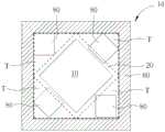
图1是根据本发明的一个实施例的半导体电子封装的俯视立体图。FIG. 1 is a top perspective view of a semiconductor electronic package according to one embodiment of the present invention.
图2是图1的虚线I-I’的示意剖视图。Fig. 2 is a schematic sectional view of the dotted line I-I' in Fig. 1 .
图3是根据本发明一个实施例的半导体电子封装的透视图。3 is a perspective view of a semiconductor electronic package according to one embodiment of the present invention.
图4是在封装基板上具有金属环和旋转的半导体晶粒的电子封装的示意性俯视图。4 is a schematic top view of an electronic package with a metal ring and a rotating semiconductor die on a package substrate.
图5是沿图4中的虚线II-II’截取的示意性剖视图。Fig. 5 is a schematic cross-sectional view taken along a dotted line II-II' in Fig. 4 .
图6是示出根据本发明另一实施例的具有金属盖的电子封装的示意性截面图。FIG. 6 is a schematic cross-sectional view showing an electronic package with a metal lid according to another embodiment of the present invention.
图7是具有金属环和旋转的半导体晶粒的电子封装的示意性顶视图,示出了根据本发明的另一实施例的在金属环与芯片封装之间的三角形区域内布置有更多的去耦电容器。7 is a schematic top view of an electronic package with a metal ring and a rotating semiconductor die, showing more chips arranged in a triangular area between the metal ring and the chip package according to another embodiment of the present invention. decoupling capacitors.
图8是具有金属环和旋转的半导体晶粒的电子封装的示意性俯视图,示出了根据本发明的另一实施例的一些芯片布置在金属环与芯片封装之间的三角形区域内。8 is a schematic top view of an electronic package with a metal ring and a rotating semiconductor die, showing some chips arranged in a triangular area between the metal ring and the chip package according to another embodiment of the present invention.
图9是根据本发明的另一个实施例的具有用于弯曲控制的延伸的金属环的电子封装的示意性顶视图。9 is a schematic top view of an electronic package with an extended metal ring for bend control according to another embodiment of the present invention.
具体实施方式Detailed ways
在本发明实施例的以下详细描述中,参考了作为本发明的一部分的附图,并且其中通过图示的方式示出了可以实践本发明的特定优选实施例。足够详细地描述了这些实施例以使本领域技术人员能够实践它们,并且应该理解,可以利用其他实施例,并且可以在不脱离本发明的精神和范围的情况下进行机械,结构和程序上的改变。因此,以下详细描述不应被视为具有限制意义,并且本发明的实施例的范围仅由所附权利要求限定。In the following detailed description of embodiments of the invention, reference is made to the accompanying drawings which form a part hereof, and in which is shown by way of illustration certain preferred embodiments in which the invention may be practiced. These embodiments have been described in sufficient detail to enable those skilled in the art to practice them, and it is to be understood that other embodiments may be utilized, and mechanical, structural, and procedural modifications may be made without departing from the spirit and scope of the invention. Change. Accordingly, the following detailed description should not be taken in a limiting sense, and the scope of embodiments of the present invention is defined only by the appended claims.
应当理解,尽管本实施例可以使用术语第一,第二,第三,主要,次要等来描述各种元件,部件,区域,层和/或部分,但是这些元件,部件,区域,层和/或部分不应受这些术语的限制。这些术语仅用于将一个元件,组件,区域,层或部分与另一个元件,组件,区域,层或部分区分开。因此,在不脱离本发明构思的教导的情况下,下面讨论的第一或主要元件,组件,区域,层或部分可以称为第二或次要元件,组件,区域,层或部分。It should be understood that although the present embodiments may use the terms first, second, third, primary, secondary, etc. to describe various elements, components, regions, layers and/or sections, these elements, components, regions, layers and and/or parts should not be limited by these terms. These terms are only used to distinguish one element, component, region, layer or section from another element, component, region, layer or section. Thus, a first or primary element, component, region, layer or section discussed below could be termed a second or secondary element, component, region, layer or section without departing from the teachings of the inventive concept.
本实施例可以使用空间相对术语,例如“在…之下”,“在…下方”,“下方”,“在…下面”,“在…之上”,“上方”,“在…上面”等,以便于描述图中一个元素或特征与另一个元素或特征的关系。应当理解,除了图中所示的方向取向之外,空间相对术语旨在包括使用或操作中的装置的不同取向。例如,如果图中的设备被翻转,则描述为在其他元件或特征“在…下方”或“在…之下”或“下方”的元件将被定向在其他元件或特征“在…之上”或“上方”。因此,示例性术语“在…下方”和“下方”可以包括上方和下方的方向。装置可以以其他方式定向(旋转90度或在其他方位),并且相应地解释本文使用的空间相对描述符。另外,还应理解,当层被称为在两个层“之间”时,它可以是两个层之间的唯一层,或者也可以存在一个或多个中间层。This embodiment can use spatially relative terms, such as "under", "below", "below", "below", "on", "above", "on" etc. , in order to describe the relationship between one element or feature and another element or feature in the figure. It will be understood that the spatially relative terms are intended to encompass different orientations of the device in use or operation in addition to the directional orientation depicted in the figures. For example, if the device in the figures is turned over, elements described as "below" or "beneath" or "beneath" other elements or features would then be oriented "above" the other elements or features or "above". Thus, the exemplary terms "below" and "beneath" can encompass both an orientation of above and below. The device may be otherwise oriented (rotated 90 degrees or at other orientations) and the spatially relative descriptors used herein interpreted accordingly. In addition, it will also be understood that when a layer is referred to as being "between" two layers, it can be the only layer between the two layers, or one or more intervening layers may also be present.
这里使用的术语仅用于描述特定实施例的目的,并不旨在限制本发明构思。如这里所使用的,单数形式“一”,“一个”和“该”,“所述”旨在也包括复数形式,除非上下文另有明确说明。将进一步理解,当在本说明书中使用时,术语“包括”和/或“包含”指定所述特征,整体,步骤,操作,元件和/或组件的存在,但不排除存在或者添加一个或多个其他特征,整体,步骤,操作,元素,组件和/或其组合。如这里所使用的,术语“和/或”包括一个或多个相关所列项目的任何和所有组合,并且可以缩写为“/”。The terminology used herein is for the purpose of describing particular embodiments only and is not intended to be limiting of the inventive concept. As used herein, the singular forms "a", "an" and "the", "the" are intended to include the plural forms as well, unless the context clearly dictates otherwise. It will be further understood that when used in this specification, the terms "comprising" and/or "comprising" specify the presence of stated features, integers, steps, operations, elements and/or components, but do not exclude the presence or addition of one or more other features, wholes, steps, operations, elements, components and/or combinations thereof. As used herein, the term "and/or" includes any and all combinations of one or more of the associated listed items and may be abbreviated as "/".
应当理解,当元件或层被称为“在…上”,“连接到”,“耦合到”或“邻接”另一个元件或层时,它可以直接在另一个元件或层的上方,直接连接,直接耦合或直接邻接于另一个元件或层,或者可以在元件或层与另一个元件或层之间存在中间元件或层。相反,当元件被称为“直接在......上”,“直接连接到”,“直接耦合到”或“直接邻接”另一元件或层时,不存在中间元件或层。It will be understood that when an element or layer is referred to as being "on," "connected to," "coupled to" or "adjacent" another element or layer, it can be directly on, directly connected to, the other element or layer , directly coupled to or directly adjacent to another element or layer, or intervening elements or layers may be present between the element or layer and another element or layer. In contrast, when an element is referred to as being "directly on," "directly connected to," "directly coupled to" or "directly adjacent to" another element or layer, there are no intervening elements or layers present.
串行器/解串器(SerDes)是高速通信中常用的一对功能块(functional block),用于补偿有限的输入/输出。这些功能块在每个方向上在串行数据(serial data)和并行接口(parallel interface)之间转换数据。术语“SerDes”通常是指在各种技术和应用程序中使用的接口。SerDes的主要用途是在单条线(single line)或差分对(differential pair)上提供数据传输,以最大程度地减少I/O引脚和互连的数量。SerDes数据传输的实现可在各种通信系统和设备中使用,例如移动设备,桌面计算机和服务器,计算机网络和电信网络。A serializer/deserializer (SerDes) is a pair of functional blocks commonly used in high-speed communications to compensate for limited input/output. These functional blocks convert data between serial data and parallel interface in each direction. The term "SerDes" generally refers to interfaces used in various technologies and applications. The main purpose of SerDes is to provide data transmission on a single line or differential pair to minimize the number of I/O pins and interconnects. The implementation of SerDes data transmission can be used in various communication systems and devices, such as mobile devices, desktop computers and servers, computer networks and telecommunication networks.
本发明所公开的电子封装配置为以每秒千兆位元(Gbps,或每秒千兆位元)数据速率运行,能够减少信号扭曲,从而改善芯片封装的电性能,该芯片封装适用于包括但不限于以下各项在内的高数据速率通信应用:超大型数据中心,超高性能网络交换机,路由器或计算应用程序以及4G和5G服务提供商(回程(backhaul))基础设施,AI(ArtificialIntelligence,人工智能)深度学习应用程序以及新颖的计算应用程序。Disclosed electronic packages configured to operate at gigabit per second (Gbps, or gigabits per second) data rates can reduce signal distortion, thereby improving the electrical performance of chip packages suitable for use in applications including High data rate communications applications including, but not limited to: hyperscale data centers, ultra-high performance network switches, routers or computing applications and 4G and 5G service provider (backhaul) infrastructure, AI (Artificial Intelligence , artificial intelligence) deep learning applications as well as novel computing applications.
请参考图1至图3。图1为根据本发明的一实施例的电子封装的俯视图。图2是沿图1中的虚线I-I’截取的示意性截面图。图3是根据本发明的一个实施例的电子封装的透视图。Please refer to Figure 1 to Figure 3. FIG. 1 is a top view of an electronic package according to an embodiment of the invention. Fig. 2 is a schematic cross-sectional view taken along the dotted line II' in Fig. 1 . Figure 3 is a perspective view of an electronic package according to one embodiment of the present invention.
如图1至图3所示,根据一个实施例,电子封装1包括芯片封装10,该芯片封装10以倒装芯片(flip-chip)的方式安装在封装基板20的顶表面201上并且可以通过凸块30接合到顶表面201。从上方看时,芯片封装10和封装基板20都可以具有矩形形状(分别具有正方形或长方形形状)。例如,芯片封装10和封装基板20都可以具有正方形形状,该正方形形状具有相等长度的四个侧面。芯片封装10具有四个侧面10a、10b、10c、10d。封装基板20具有四个顶点


如图1所示,封装基板20的顶表面201可以通过在二维平面(平行于顶表面201)中的两个正交轴(参考X和Y轴)划分成四个90度象限

根据一个实施例,封装基板20可以是有机基板,其包括层压的有机材料或芯200,例如环氧树脂等。如图2所示,一个或多个焊球230可以布置在封装基板20的底表面202上。芯片封装10通过多个焊点或凸块30安装在封装基板20的顶表面201上。底部填充物40可以分配以填充芯片封装10和封装基板20之间的间隙(或支座(standoff))。封装基板20可以包括多层迹线,例如迹线211和221。According to one embodiment, the
在图2中,迹线211可以在设置在封装基板20的多层迹线的最顶层中。通常,迹线211可以覆盖有保护层280,例如阻焊剂等,但不限于此。凸块30与例如位于迹线211的一个远程处的对应的凸块焊盘210接合并对准(或对齐,可以指凸块30与凸块焊盘210在俯视方向上至少部分地重叠)。迹线211朝向顶点A处的拐角或朝向围绕该拐角的两个相邻侧面20a和20b延伸。In FIG. 2 ,
用于电连接相应的凸块焊盘210的迹线211通常设置在本实施例的象限Q2内。迹线211电耦合到连接焊盘212,也就是说凸块焊盘210通过迹线211连接到连接焊盘212。可以设置电镀通孔(plated through hole,PTH)213以将连接焊盘212电连接到封装基板20的底表面202处的焊球焊盘214。焊球230焊在焊球焊盘214上,以进一步与系统板或印刷电路板(printed circuit board,PCB)连接。
为了简单起见,如图1所示,仅示出在象限Q2内的迹线和焊球布置。在图1中未明确示出焊球230。然而,可以理解,由于连接焊盘212与焊球焊盘214对齐(例如完全对齐或有错开的对齐,例如有部分重叠而有部分未重叠),因此连接焊盘212与焊球230对齐(例如至少部分地对齐),因此,图1中每个连接焊盘212的位置通常代表每个焊球230的位置(也就是说,每个连接焊盘212的下方均可以设有相应的焊球230)。可以理解,在其他实施例中,象限Q2中所示的上述配置可以用于其他象限Q1,Q3和Q4。For simplicity, as shown in FIG. 1 , only the trace and ball arrangement in quadrant Q2 is shown.
如图1和图3所示,芯片封装10和封装基板20可以具有相同的中心点CP,因此芯片封装具有相对于封装基板20成角度偏移的同心构造。例如,芯片封装10相对于封装基板20在Z轴上方旋转大约45度的旋转偏移角θ(也就是说,芯片封装10的对角线相对于封装基板20的对角线之间具有大约45度的夹角,当然也可以是其他角度,例如30到75度等),其中旋转偏移角θ是参考Y轴与芯片封装10的侧面10b或10d方向之间的夹角。根据一个实施例,芯片封装10的四个侧面10a至10d中的任何一个都不与封装基板20的四个侧面20a至20d中的任何一个平行。As shown in FIGS. 1 and 3 , the
旋转芯片封装10,使得其一侧10a直接面对封装基板20的顶点A处的一个拐角(也即面对顶点A处的角)。封装基板20的两个侧面20a和20b在顶点A处接合。这两个侧面20a和20b定义了90度象限Q2的边界。The
根据一个实施例,芯片封装10包括第一高速接口电路晶粒11,其可以以至少1000Mbps的高速数据传输速率在高于500MHz的频率下运转。如图2所示,第一高速接口电路晶粒11可以封装在模塑料50内。根据一个实施例,第一高速接口电路晶粒11包括第一串行器/解串器(SerDes)电路块110,位于紧靠侧面10a的附近,侧面10a直接面向封装基板20的顶点A的拐角。According to one embodiment, the
根据一个实施例,如图1所示,第一高速接口电路晶粒11包括直接面对封装基板20的顶点A处的拐角的第一边缘11a,垂直于第一边缘11a并连接到第一边缘11a的第二边缘11b,垂直于第一边缘11a并连接到第一边缘11a的第三边缘11c。根据一个实施例,第一边缘11a与芯片封装10的侧面10a平行,第二边缘11b与芯片封装10的侧面10d平行,并且第三边缘11c与侧面10b平行。第二边缘11b和第三边缘11c与在顶点A和顶点C之间延伸的对角线DL平行。According to one embodiment, as shown in FIG. 1 , the first high-speed interface circuit die 11 includes a
根据一个实施例,如图1所示,第一排输入/输出(input/output,I/O)焊盘111a沿着第一边缘11a布置,第二排I/O焊盘111b沿着第二边缘11b布置,第三排I/O焊盘111c沿第三边缘11c设置。可以理解,这些I/O焊盘111设置在第一高速接口电路晶粒11的底部。According to one embodiment, as shown in FIG. 1 , a first row of input/output (I/O)
根据一个实施例,可以在第一高速接口电路晶粒11和封装基板20的顶表面201之间提供重分布层(redistribution layer,RDL)结构100,以将I/O焊盘111分散开。在本领域中已知的RDL结构100可以由介电层和介电层中的互连结构组成,以将高速接口电路晶粒11的I/O焊盘电连接到形成在凸块30上的相应的凸块焊盘101。根据一个实施例,芯片封装10可以是扇出芯片级封装(fan-out wafer level package,FOWLP)。According to one embodiment, a redistribution layer (RDL)
根据一个实施例,第一高速接口电路晶粒11的第一SerDes电路块110,边缘11a至11c,I/O焊盘排111a至111c(第一排I/O焊盘111a,第二排I/O焊盘111b,第三排I/O焊盘111c)通常设置在示例性象限Q2内。可以理解,芯片封装10倒装,芯片封装10的有源表面(active surface)以倒装芯片的方式安装在封装基板20的顶表面201上。According to one embodiment, the first
如图1所示,根据一个实施例,沿着在顶点A处接合的两个侧面20a和20b布置第一组焊球P1(焊球未在图1中明确示出,但与连接焊盘212a对齐,例如设置在连接焊盘212a的下方)。在封装基板20的顶表面201上的象限Q2内,布置在第一高速接口电路晶粒11的第一边缘11a处的第一排I/O焊盘111a分别通过迹线211a电连接到第一组焊球P1。As shown in FIG. 1, according to one embodiment, a first set of solder balls P1 are arranged along the two
根据一个实施例,第二组焊球P2(焊球未在图1中明确示出,但与连接焊盘212b对齐,例如设置在连接焊盘212b的下方)沿着与顶点A处的拐角相邻的侧面20a布置。在封装基板20的顶表面201上的象限Q2内,第二排I/O焊盘111b分别通过迹线211b电连接到第二组焊球P2。According to one embodiment, a second group of solder balls P2 (solder balls not explicitly shown in FIG. The
根据一个实施例,第三组焊球P3(焊球未在图1中明确示出,但与连接焊盘212c对准)沿着与顶点A处的拐角相邻的侧面20b布置。在封装基板20的顶面201上的象限Q2内,第三排I/O焊盘111c分别通过迹线211c电连接到第三组焊球P3。According to one embodiment, a third set of solder balls P3 (solder balls not explicitly shown in FIG. 1 , but aligned with
根据一个实施例,如图2所示,芯片封装10还可以包括在第一高速接口电路晶粒11附近的第二高速接口电路晶粒12。第二高速接口电路晶粒12可以是包括SerDes电路块120,并且可以在封装基板20的顶表面201的象限Q4中具有类似的迹线和球形布置。第一高速接口电路晶粒11可以通过RDL结构100电连接到第二高速接口电路晶粒12。例如,第一高速接口电路晶粒11的I/O焊盘111d通过RDL结构100中的互联机103电连接到第二高速接口电路晶粒12的I/O焊盘121d。在象限Q4中,第二高速接口电路晶粒12上的I/O焊盘可以采用与第一高速接口电路晶粒11相类似的迹线布置,从而降低从晶粒到焊球之间的迹线长度或线路长度。According to an embodiment, as shown in FIG. 2 , the
使用本发明是有利的,因为通过提供旋转的芯片封装配置,封装基板上的相应迹线和焊球布置集中在四个象限Q1至Q4中的一个之内,这样使得最大信号长度减少14.3%。(例如,对于
值得注意的是,尽管在说明性实施例中使用了大约45度的旋转偏移角θ,但是在其他实施例中,电子封装1中的旋转晶粒设计不限于该角度。例如,在一些实施例中,旋转偏移角θ可以在30度和75度之间的范围内。It is worth noting that although a rotational offset angle θ of approximately 45 degrees is used in the illustrative embodiment, in other embodiments the rotational die design in
图4和图5示出了在封装基板上具有金属环和旋转的半导体晶粒的电子封装,其中,相似的层,元件或区域由相似的数字和标注表示。如图4和图5所示,根据一个实施例的电子封装1a可以包括金属环(或金属框架)60,该金属环60通过粘合剂层610粘附到封装基板20的顶表面201。在实施例中,金属环60可以是铜环,但不限于此。根据一些实施例,封装基板20具有矩形形状并且具有四个角。4 and 5 illustrate an electronic package with a metal ring and a rotating semiconductor die on a package substrate, wherein like layers, elements or regions are indicated by like numerals and labels. As shown in FIGS. 4 and 5 , the electronic package 1 a according to one embodiment may include a metal ring (or metal frame) 60 adhered to the
如前所述,芯片封装10包括安装在封装基板20的顶表面201上的第一高速接口电路晶粒11和设置在第一高速接口电路晶粒11附近的第二高速接口电路晶粒12。芯片封装10,第一高速接口电路晶粒11和第二高速接口电路晶粒12相对于封装基板20在垂直轴(图5中的Z轴)上方旋转。垂直轴通过旋转偏移角θ垂直于顶表面201。As mentioned above, the
如图4中的虚线所示,封装基板20上的旋转芯片封装10可以在电子封装1a的四个角中的每个角处的三角形区域T中提供一些空间,以用于改善翘曲控制或电气性能。其中,在电子封装的四个角中的每个角处的区域未必一定是三角形的,可以是其他形状,或开放的区域,因此可称为在金属环和旋转的芯片封装的侧面之间的区域。其中,在图4所示的实施例中,当旋转偏移角为45度时,芯片封装10的拐角处距离金属环60的距离几乎是最小的,因此在电子封装的四个角中的每个角处的区域位置或面积较大(或者三角形区域T的面积较大),因此可以方便在该区域布置元器件,例如布置更多的电容器等等;或者金属环60可以在该区域上具有延伸的结构(例如如下图9所示),这样可以使金属环具有更大的覆盖面积,从而进一步防止封装的翘曲和开裂等问题,提高封装的机械强度。另外,旋转偏移角也可以为其他角度,例如上述提到的30-75度,这可以根据芯片封装10的大小和形状以及封装基板20的大小和形状来共同确定,当然可以调整旋转偏移角以使在电子封装的四个角中的每个角处的区域位置或面积较大(或者三角形区域T的面积较大)。此外图4中虚线所示的三角形区域T仅是为了示意,并非实际的元器件的划线。As shown by the dotted lines in FIG. 4 , rotating the
应该理解,如图6所示,在一些实施例中,金属环60可以用覆盖芯片封装10的顶表面的金属盖60a代替。在图6中,电子封装1b的模塑料50可以抛光直到暴露出第一高速接口电路晶粒11和第二高速接口电路晶粒12的顶表面。金属盖60a可以与第一高速接口电路晶粒11和第二高速接口电路晶粒12的暴露的顶表面热接触。金属盖60a可以是一体的结构,以加强封装的机械强度,更好的防止翘曲。It should be understood that, as shown in FIG. 6 , in some embodiments, the
根据一些实施例,如图7所示,金属环60和芯片封装10之间的三角形区域T可用于在四个角中的每个角落的三角形区域T中容纳更多的去耦电容器(decoupling capacitor)70。因此,电子封装1c在封装的拐角处包括更多的去耦电容器,从而改善了电性能,例如配电网络(power distribution network,PDN)的性能。According to some embodiments, as shown in FIG. 7 , the triangular area T between the
根据一些实施例,至少一个去耦电容器70可以设置在封装基板1c的拐角处(或角落处或角部),其中,去耦电容器70相对于封装基板20在垂直于顶表面201的垂直轴(图5中的Z轴)的上方旋转偏移角θ。也就是说,去耦电容器70可以与芯片封装10具有相同的旋转角度,以方便布线连接以及充分利用到电子封装角落处的区域。According to some embodiments, at least one
根据一些实施例,如图8所示,金属环60和芯片封装10之间的三角形区域T可以用于容纳更多的芯片80或更大尺寸的芯片。布置在三角形区域T内的芯片80可以旋转或不旋转,例如一个或一些芯片80可以与芯片封装10具有相同的旋转角度,另一个或另一些芯片80相对于封装基板20未旋转。通过在电子封装1d中提供这样的配置,多芯片模块可以更大并且更对称,从而导致更好的封装翘曲控制和改善的电性能。模块可以是模制型(molding-type,其可具有或不具有功能)封装,以平衡热膨胀系数(coefficient of thermalexpansion,CTE)不匹配并改善封装翘曲。According to some embodiments, as shown in FIG. 8 , the triangular area T between the
根据一些实施例,如图9所示,金属环90可包括在金属环90和芯片封装10之间的三角形区域T(如图4或图9中的虚线所示)内的延伸部分90a,该延伸部分90a与金属环90可以是一体结构或整体结构。封装翘曲控制由于在电子封装1f的四个角处竖立的较宽的环形脚而得到改进。根据本发明的上述方式,通过将芯片封装10进行旋转而使得在电子封装的角落位置处留出了空置区域,这样可以设置该延伸部分90a,从而在没有明显加宽金属环90的侧面宽度的情况下,增加金属环90的覆盖面积,从而进一步防止封装的翘曲和开裂等问题,提高封装的机械强度;同时本发明的上述方式在电子封装有限的空间中扩展了金属环的结构和安装方式,提高了空间利用率,相比先前技术以低成本的方式降低了封装翘曲的可能性,加强了封装强度(先前技术中可能需要增加金属环的侧面宽度来提高封装强度,然而这受到电子封装空间的限制,并且影响基板走线设计)。金属环可以控制常规大尺寸芯片封装的共面性(coplanarity)和翘曲,并且本实施例中通过将芯片封装10进行旋转,不仅优化了基板走线设计,基板标记(例如条形码,基准标记等),而且还优化了基板拐角处的金属环/盖的足宽设计,具有较佳的应用优势。According to some embodiments, as shown in FIG. 9 , the
本领域的技术人员将容易地观察到,在保持本发明教导的同时,可以做出许多该装置和方法的修改和改变。因此,上述公开内容应被解释为仅由所附权利要求书的界限和范围所限制。Those skilled in the art will readily observe that many modifications and variations of this apparatus and method can be made while maintaining the teachings of the present invention. Accordingly, the foregoing disclosure should be construed as being limited only by the metes and bounds of the appended claims.
Claims (10)
Translated fromChinesePriority Applications (1)
| Application Number | Priority Date | Filing Date | Title |
|---|---|---|---|
| CN202310021282.2ACN115985861A (en) | 2019-05-15 | 2020-04-24 | electronic packaging |
Applications Claiming Priority (4)
| Application Number | Priority Date | Filing Date | Title |
|---|---|---|---|
| US201962848064P | 2019-05-15 | 2019-05-15 | |
| US62/848,064 | 2019-05-15 | ||
| US16/846,381US11222850B2 (en) | 2019-05-15 | 2020-04-12 | Electronic package with rotated semiconductor die |
| US16/846,381 | 2020-04-12 |
Related Child Applications (1)
| Application Number | Title | Priority Date | Filing Date |
|---|---|---|---|
| CN202310021282.2ADivisionCN115985861A (en) | 2019-05-15 | 2020-04-24 | electronic packaging |
Publications (2)
| Publication Number | Publication Date |
|---|---|
| CN111952256A CN111952256A (en) | 2020-11-17 |
| CN111952256Btrue CN111952256B (en) | 2023-02-07 |
Family
ID=70483040
Family Applications (2)
| Application Number | Title | Priority Date | Filing Date |
|---|---|---|---|
| CN202310021282.2APendingCN115985861A (en) | 2019-05-15 | 2020-04-24 | electronic packaging |
| CN202010332486.4AActiveCN111952256B (en) | 2019-05-15 | 2020-04-24 | electronic packaging |
Family Applications Before (1)
| Application Number | Title | Priority Date | Filing Date |
|---|---|---|---|
| CN202310021282.2APendingCN115985861A (en) | 2019-05-15 | 2020-04-24 | electronic packaging |
Country Status (4)
| Country | Link |
|---|---|
| US (3) | US11222850B2 (en) |
| EP (1) | EP3739626A1 (en) |
| CN (2) | CN115985861A (en) |
| TW (1) | TWI719897B (en) |
Families Citing this family (8)
| Publication number | Priority date | Publication date | Assignee | Title |
|---|---|---|---|---|
| US11222850B2 (en)* | 2019-05-15 | 2022-01-11 | Mediatek Inc. | Electronic package with rotated semiconductor die |
| TWI735398B (en)* | 2020-12-21 | 2021-08-01 | 矽品精密工業股份有限公司 | Electronic package and manufacturing method thereof |
| US11562962B2 (en)* | 2021-01-13 | 2023-01-24 | Qualcomm Incorporated | Package comprising a substrate and interconnect device configured for diagonal routing |
| CN114496971A (en)* | 2021-05-05 | 2022-05-13 | 威盛电子股份有限公司 | Packaging substrate, chip packaging body and integrated circuit chip |
| TWI819441B (en)* | 2021-05-05 | 2023-10-21 | 威盛電子股份有限公司 | Package substrate, chip package and integrated circuit chip |
| DE102021120398B4 (en)* | 2021-08-05 | 2023-03-02 | Infineon Technologies Ag | SYSTEMS AND DEVICES FOR WHEEL SENSORS |
| CN114927491A (en)* | 2022-05-17 | 2022-08-19 | 超聚变数字技术有限公司 | Electronic device, circuit board and chip |
| US20230395524A1 (en)* | 2022-06-06 | 2023-12-07 | Intel Corporation | Emi cage for microstrip routing via dual layer underfill concept |
Citations (3)
| Publication number | Priority date | Publication date | Assignee | Title |
|---|---|---|---|---|
| US4705917A (en)* | 1985-08-27 | 1987-11-10 | Hughes Aircraft Company | Microelectronic package |
| CN108028225A (en)* | 2015-09-17 | 2018-05-11 | 德卡技术股份有限公司 | Thermal-enhanced full molding is fanned out to module |
| CN108807283A (en)* | 2017-04-28 | 2018-11-13 | 台湾积体电路制造股份有限公司 | Semiconductor packaging structure |
Family Cites Families (21)
| Publication number | Priority date | Publication date | Assignee | Title |
|---|---|---|---|---|
| JP2002290030A (en) | 2001-03-23 | 2002-10-04 | Ngk Spark Plug Co Ltd | Wiring board |
| DE10202878A1 (en)* | 2002-01-25 | 2003-08-07 | Infineon Technologies Ag | Circuit board with integrated circuit for high speed data processing |
| TW571407B (en)* | 2002-10-25 | 2004-01-11 | Advanced Semiconductor Eng | Construction of a package with multiple modules |
| US8237289B2 (en) | 2007-01-30 | 2012-08-07 | Kabushiki Kaisha Toshiba | System in package device |
| JP2008218669A (en)* | 2007-03-02 | 2008-09-18 | Nec Electronics Corp | Semiconductor device |
| JP5313887B2 (en)* | 2007-05-31 | 2013-10-09 | 三洋電機株式会社 | Semiconductor module and portable device |
| TWI335055B (en)* | 2007-06-29 | 2010-12-21 | Chipmos Technologies Inc | Chip-stacked package structure |
| JP2009283835A (en)* | 2008-05-26 | 2009-12-03 | Elpida Memory Inc | Semiconductor device and method of manufacturing the same |
| US7884470B2 (en) | 2008-12-23 | 2011-02-08 | Intel Corporation | Semiconductor packages with stiffening support for power delivery |
| JP5511823B2 (en)* | 2009-08-07 | 2014-06-04 | パナソニック株式会社 | Semiconductor device and electronic device |
| US20130256883A1 (en) | 2012-03-27 | 2013-10-03 | Intel Mobile Communications GmbH | Rotated semiconductor device fan-out wafer level packages and methods of manufacturing rotated semiconductor device fan-out wafer level packages |
| US20140048951A1 (en) | 2012-08-14 | 2014-02-20 | Bridge Semiconductor Corporation | Semiconductor assembly with dual connecting channels between interposer and coreless substrate |
| US9147667B2 (en)* | 2013-10-25 | 2015-09-29 | Bridge Semiconductor Corporation | Semiconductor device with face-to-face chips on interposer and method of manufacturing the same |
| US9281296B2 (en) | 2014-07-31 | 2016-03-08 | Invensas Corporation | Die stacking techniques in BGA memory package for small footprint CPU and memory motherboard design |
| US10242957B2 (en)* | 2015-02-27 | 2019-03-26 | Qualcomm Incorporated | Compartment shielding in flip-chip (FC) module |
| KR20180109850A (en)* | 2016-02-10 | 2018-10-08 | 르네사스 일렉트로닉스 가부시키가이샤 | Semiconductor device |
| US10629545B2 (en) | 2017-03-09 | 2020-04-21 | Taiwan Semiconductor Manufacturing Company Ltd. | Semiconductor device |
| KR102439761B1 (en)* | 2017-12-22 | 2022-09-02 | 삼성전자주식회사 | Electronic devices and methods of manufacturing electronic devices |
| US20190355697A1 (en)* | 2018-05-18 | 2019-11-21 | Mediatek Inc. | Electronic package for high-data rate communication applications |
| US20230154893A1 (en)* | 2018-12-07 | 2023-05-18 | Amkor Technology Singapore Holding Pte. Ltd. | Semiconductor package and fabricating method thereof |
| US11222850B2 (en)* | 2019-05-15 | 2022-01-11 | Mediatek Inc. | Electronic package with rotated semiconductor die |
- 2020
- 2020-04-12USUS16/846,381patent/US11222850B2/enactiveActive
- 2020-04-24CNCN202310021282.2Apatent/CN115985861A/enactivePending
- 2020-04-24CNCN202010332486.4Apatent/CN111952256B/enactiveActive
- 2020-04-30EPEP20172494.5Apatent/EP3739626A1/enactivePending
- 2020-05-12TWTW109115743Apatent/TWI719897B/enactive
- 2021
- 2021-12-16USUS17/553,760patent/US11830820B2/enactiveActive
- 2023
- 2023-10-24USUS18/383,466patent/US12388026B2/enactiveActive
Patent Citations (3)
| Publication number | Priority date | Publication date | Assignee | Title |
|---|---|---|---|---|
| US4705917A (en)* | 1985-08-27 | 1987-11-10 | Hughes Aircraft Company | Microelectronic package |
| CN108028225A (en)* | 2015-09-17 | 2018-05-11 | 德卡技术股份有限公司 | Thermal-enhanced full molding is fanned out to module |
| CN108807283A (en)* | 2017-04-28 | 2018-11-13 | 台湾积体电路制造股份有限公司 | Semiconductor packaging structure |
Also Published As
| Publication number | Publication date |
|---|---|
| CN111952256A (en) | 2020-11-17 |
| US20220108954A1 (en) | 2022-04-07 |
| US20200365515A1 (en) | 2020-11-19 |
| US12388026B2 (en) | 2025-08-12 |
| TW202044496A (en) | 2020-12-01 |
| US20240055358A1 (en) | 2024-02-15 |
| US11830820B2 (en) | 2023-11-28 |
| TWI719897B (en) | 2021-02-21 |
| US11222850B2 (en) | 2022-01-11 |
| CN115985861A (en) | 2023-04-18 |
| EP3739626A1 (en) | 2020-11-18 |
Similar Documents
| Publication | Publication Date | Title |
|---|---|---|
| CN111952256B (en) | electronic packaging | |
| US11862602B2 (en) | Scalable architecture for reduced cycles across SOC | |
| US11569208B2 (en) | Semiconductor structure and method for making thereof | |
| US9460937B2 (en) | Hybrid substrates, semiconductor packages including the same and methods for fabricating semiconductor packages | |
| KR100368696B1 (en) | Semiconductor device, and method for manufacturing the same | |
| US11664331B2 (en) | Semiconductor package | |
| TWI697084B (en) | Rlink - ground shielding attachment structures and shadow voiding for data signal contacts of package devices; vertical ground shielding structures and shield fencing of vertical data signal interconnects of package devices; and ground shielding for electro optical module connector data signal contacts and contact pins of package devices | |
| JP6534386B2 (en) | Techniques for controlling the position of stacked dies | |
| US20190355697A1 (en) | Electronic package for high-data rate communication applications | |
| US20250029911A1 (en) | Manufacturing method of semiconductor substrate | |
| CN110911384A (en) | An embedded passive bridge chip and its application | |
| US20240038721A1 (en) | Semiconductor devices and methods of manufacturing thereof | |
| CN111769101B (en) | Packaging structure and packaging method based on multiple transfer boards | |
| CN111863756B (en) | Packaging structure and semiconductor device with same | |
| TW202117943A (en) | Multi-chip three-dimensional stacked package with fan-out structure | |
| US20250140770A1 (en) | Electronic package and manufacturing method thereof | |
| CN115497901B (en) | High-density packaging device and method for improving bump cracking failure | |
| TWI776710B (en) | Interposer and semiconductor package | |
| WO2025156634A1 (en) | Interconnection interposer component, chip packaging system, and electronic device | |
| KR20240045008A (en) | Semiconductor package | |
| KR20240113267A (en) | Semiconductor package | |
| CN117316890A (en) | Chip packaging structure, preparation method thereof and electronic equipment |
Legal Events
| Date | Code | Title | Description |
|---|---|---|---|
| PB01 | Publication | ||
| PB01 | Publication | ||
| SE01 | Entry into force of request for substantive examination | ||
| SE01 | Entry into force of request for substantive examination | ||
| GR01 | Patent grant | ||
| GR01 | Patent grant |