CN111950324A - An ultrasonic sensor and its manufacturing method and display panel - Google Patents
An ultrasonic sensor and its manufacturing method and display panelDownload PDFInfo
- Publication number
- CN111950324A CN111950324ACN201910402605.6ACN201910402605ACN111950324ACN 111950324 ACN111950324 ACN 111950324ACN 201910402605 ACN201910402605 ACN 201910402605ACN 111950324 ACN111950324 ACN 111950324A
- Authority
- CN
- China
- Prior art keywords
- electrodes
- electrode
- ultrasonic sensor
- receiving
- transmitting
- Prior art date
- Legal status (The legal status is an assumption and is not a legal conclusion. Google has not performed a legal analysis and makes no representation as to the accuracy of the status listed.)
- Granted
Links
Images


Classifications
- G—PHYSICS
- G06—COMPUTING OR CALCULATING; COUNTING
- G06V—IMAGE OR VIDEO RECOGNITION OR UNDERSTANDING
- G06V40/00—Recognition of biometric, human-related or animal-related patterns in image or video data
- G06V40/10—Human or animal bodies, e.g. vehicle occupants or pedestrians; Body parts, e.g. hands
- G06V40/12—Fingerprints or palmprints
- G06V40/13—Sensors therefor
- G06V40/1306—Sensors therefor non-optical, e.g. ultrasonic or capacitive sensing
Landscapes
- Engineering & Computer Science (AREA)
- Human Computer Interaction (AREA)
- Physics & Mathematics (AREA)
- General Physics & Mathematics (AREA)
- Multimedia (AREA)
- Theoretical Computer Science (AREA)
- Transducers For Ultrasonic Waves (AREA)
- Ultra Sonic Daignosis Equipment (AREA)
Abstract
Translated fromChinese
Description
Translated fromChinese技术领域technical field
本发明涉及传感器技术领域,特别涉及一种超声波传感器及其制作方法和显示面板。The present invention relates to the technical field of sensors, in particular to an ultrasonic sensor and a manufacturing method thereof and a display panel.
背景技术Background technique
随着显示技术的高速发展,具有生物识别功能的电子设备逐渐进入人们的生活与工作中。例如超声波指纹识别技术是生物识别技术中应用较为广泛的技术之一。With the rapid development of display technology, electronic devices with biometric functions have gradually entered people's life and work. For example, ultrasonic fingerprint recognition technology is one of the widely used technologies in biometrics.
目前的超声波指纹识别技术中,超声波传感器的发射电极和接收电极同时进行信号的收发,发射电极的发射波有可能发射到与之对应的接收电极的相邻接收电极上,即产生信号在相邻的接收电极之间发生串扰的现象,进而导致传感器的信号接收量较低,影响指纹识别的质量。In the current ultrasonic fingerprint recognition technology, the transmitting and receiving electrodes of the ultrasonic sensor transmit and receive signals at the same time. The phenomenon of crosstalk occurs between the receiving electrodes of the sensor, which in turn leads to a low signal reception of the sensor, which affects the quality of fingerprint recognition.
发明内容SUMMARY OF THE INVENTION
本申请实施例提供一种超声波传感器及其制作方法和显示面板,用于提高超声波传感器的信号接收量,提升指纹识别的质量。Embodiments of the present application provide an ultrasonic sensor, a manufacturing method thereof, and a display panel, which are used to improve the signal reception of the ultrasonic sensor and improve the quality of fingerprint recognition.
第一方面,本申请实施例提供了一种超声波传感器,该超声波传感器包括承载基板,以及在所述承载基板上阵列设置的多个接收电极、位于所述多个接收电极上的压电膜层,以及位于所述压电膜层上且与所述多个接收电极相对设置的多个发射电极,一个所述接收电极对应一个所述发射电极;其中,In a first aspect, an embodiment of the present application provides an ultrasonic sensor, the ultrasonic sensor includes a carrier substrate, a plurality of receiving electrodes arranged in an array on the carrier substrate, and a piezoelectric film layer located on the plurality of receiving electrodes , and a plurality of transmitting electrodes located on the piezoelectric film layer and opposite to the plurality of receiving electrodes, one of the receiving electrodes corresponds to one of the transmitting electrodes; wherein,
任意一个发射电极与相对的接收电极在所述承载基板的正投影具有重叠区域,且与所述相对的接收电极周围的接收电极在所述承载基板的正投影互不交叠。Any one of the transmitting electrodes and the opposite receiving electrode has an overlapping area on the orthographic projection of the carrier substrate, and does not overlap with the orthographic projection of the receiving electrode around the opposite receiving electrode on the carrier substrate.
在一种可能的实施方式中,任意一个所述发射电极在所述承载基板的正投影完全覆盖相对的接收电极在所述承载基板的正投影;或者,In a possible implementation manner, the orthographic projection of any one of the transmitting electrodes on the carrier substrate completely covers the orthographic projection of the opposite receiving electrode on the carrier substrate; or,
任意一个所述接收电极在所述承载基板的正投影完全覆盖相对的发射电极在所述承载基板的正投影;或者,The orthographic projection of any one of the receiving electrodes on the carrier substrate completely covers the orthographic projection of the opposite emitter electrode on the carrier substrate; or,
任意一个所述接收电极在所述承载基板的正投影与相对的发射电极在所述承载基板的正投影相互重合。The orthographic projection of any one of the receiving electrodes on the carrier substrate coincides with the orthographic projection of the opposite emitter electrode on the carrier substrate.
在一种可能的实施方式中,每个发射电极在所述承载基板的正投影为正方形。In a possible implementation manner, the orthographic projection of each emitter electrode on the carrier substrate is a square.
在一种可能的实施方式中,相邻的两个发射电极之间的连接构件在所述承载基板的正投影为正方形。In a possible implementation manner, the orthographic projection of the connection member between two adjacent emitter electrodes on the carrier substrate is a square.
在一种可能的实施方式中,该超声波传感器还包括:In a possible implementation, the ultrasonic sensor further includes:
位于多个所述发射电极远离多个所述接收电极一侧的保护层。a protective layer on one side of the plurality of transmitting electrodes away from the plurality of receiving electrodes.
在一种可能的实施方式中,每个所述发射电极沿所述超声传感器的厚度方向的厚度位于[3μm,30μm]范围内。In a possible implementation, the thickness of each of the transmitting electrodes along the thickness direction of the ultrasonic sensor is in the range of [3 μm, 30 μm].
在一种可能的实施方式中,该超声波传感器还包括:In a possible implementation, the ultrasonic sensor further includes:
位于所述保护层和多个所述发射电极之间的背衬电极层;a backing electrode layer between the protective layer and a plurality of the emitter electrodes;
位于多个所述发射电极和所述背衬电极层之间的绝缘层;an insulating layer between a plurality of the emitter electrodes and the backing electrode layer;
其中,每个所述发射电极和所述背衬电极层的总厚度沿所述超声传感器的厚度方向的厚度位于[10μm,20μm]范围内。Wherein, the thickness of the total thickness of each of the emitter electrode and the backing electrode layer along the thickness direction of the ultrasonic sensor is in the range of [10 μm, 20 μm].
在一种可能的实施方式中,所述绝缘层的厚度小于1μm。In a possible implementation manner, the thickness of the insulating layer is less than 1 μm.
在一种可能的实施方式中,相邻的两个所述发射电极之间还填充有第一介质材料,以使得所述压电膜层与所述多个发射电极相邻的表面平坦。In a possible implementation manner, a first dielectric material is further filled between two adjacent emitter electrodes, so that the surfaces of the piezoelectric film layer adjacent to the plurality of emitter electrodes are flat.
在一种可能的实施方式中,相邻的两个所述接收电极之间设置有第二介质材料,以使得所述压电膜层与所述多个接收电极相邻的表面平坦。In a possible implementation manner, a second dielectric material is disposed between two adjacent receiving electrodes, so that the surfaces of the piezoelectric film layer adjacent to the plurality of receiving electrodes are flat.
第二方面,本申请实施例提供了一种显示面板,该显示面板包括显示背板,以及位于所述显示背板一侧的如第一方面任一所述的超声波传感器;其中,所述显示背板的衬底基板为所述超声波传感器的承载基板。In a second aspect, an embodiment of the present application provides a display panel, the display panel includes a display backplane, and the ultrasonic sensor according to any one of the first aspects located on one side of the display backplane; wherein the display The base substrate of the backplane is the carrier substrate of the ultrasonic sensor.
第三方面,本申请实施例提供了一种超声波传感器的制作方法,该方法包括:In a third aspect, an embodiment of the present application provides a method for manufacturing an ultrasonic sensor, the method comprising:
在承载基板上依次制作阵列设置的多个接收电极、压电膜层,以及阵列设置的多个发射电极;其中,A plurality of receiving electrodes arranged in an array, a piezoelectric film layer, and a plurality of emitting electrodes arranged in an array are sequentially fabricated on the carrier substrate; wherein,
一个所述接收电极对应一个所述发射电极,且任意一个发射电极与相对的接收电极在所述承载基板的正投影具有重叠区域,且与所述相对的接收电极周围的接收电极在所述承载基板的正投影互不交叠。One of the receiving electrodes corresponds to one of the transmitting electrodes, and any one of the transmitting electrodes and the opposite receiving electrodes have an overlapping area on the orthographic projection of the carrier substrate, and the receiving electrodes around the opposite receiving electrodes are on the carrier substrate. The orthographic projections of the substrates do not overlap each other.
在一种可能的实施方式中,在所述压电膜层上制作阵列设置的多个发射电极,包括:In a possible implementation manner, a plurality of emitter electrodes arranged in an array are fabricated on the piezoelectric film layer, including:
在所述压电膜层上制作第一介质材料层;forming a first dielectric material layer on the piezoelectric film layer;
对所述第一介质材料层进行图案化处理,形成多个发射电极层的互补图案;patterning the first dielectric material layer to form a plurality of complementary patterns of the emitter electrode layers;
在图案化后的所述第一介质材料层上制作发射电极材料,形成所述多个发射电极。Emitter electrode material is fabricated on the patterned first dielectric material layer to form the plurality of emitter electrodes.
在一种可能的实施方式中,在所述压电膜层上制作阵列设置的多个发射电极,包括:In a possible implementation manner, a plurality of emitter electrodes arranged in an array are fabricated on the piezoelectric film layer, including:
在所述压电膜层上制作发射电极材料;making an emitter electrode material on the piezoelectric film layer;
对所述发射电极材料进行图案化处理,形成所述多个发射电极。The emitter electrode material is patterned to form the plurality of emitter electrodes.
在一种可能的实施方式中,在所述压电膜层上制作阵列设置的多个发射电极之后,还包括:In a possible implementation manner, after fabricating a plurality of emitter electrodes arranged in an array on the piezoelectric film layer, the method further includes:
在相邻的两个发射电极之间填充第二介质材料,以使得所述压电膜层与所述多个发射电极相邻的表面平坦;Filling a second dielectric material between two adjacent emitter electrodes, so that the surfaces of the piezoelectric film layer adjacent to the plurality of emitter electrodes are flat;
在所述多个发射电极上制作保护层。A protective layer is formed on the plurality of emitter electrodes.
在一种可能的实施方式中,所述在相邻的两个发射电极之间填充第二介质材料之后,还包括:In a possible implementation manner, after the second dielectric material is filled between two adjacent emitter electrodes, the method further includes:
在所述多个发射电极上制作绝缘层;forming an insulating layer on the plurality of emitter electrodes;
在所述绝缘层上制作背衬电极层。A backing electrode layer is formed on the insulating layer.
本申请实施例中,超声波传感器包括阵列设置的多个接收电极和多个发射电极,其中,任意一个发射电极与相对的接收电极在承载基板的正投影具有重叠区域,且与相对的接收电极周围的接收电极在承载基板的正投影互不交叠,这样即使发射电极和接收电极同时进行信号的收发,接收电极的发射波也不会发射到与之对应的接收电极的相邻接收电极上,从而避免了信号在相邻的接收电极之间可能发生串扰的问题,提高了超声波传感器的信号接收量。In the embodiment of the present application, the ultrasonic sensor includes a plurality of receiving electrodes and a plurality of transmitting electrodes arranged in an array, wherein any one of the transmitting electrodes and the opposite receiving electrode has an overlapping area on the orthographic projection of the carrier substrate, and has an overlapping area with the surrounding area of the opposite receiving electrode. The orthographic projections of the receiving electrodes on the carrier substrate do not overlap each other, so that even if the transmitting electrodes and the receiving electrodes transmit and receive signals at the same time, the transmitting waves of the receiving electrodes will not be transmitted to the adjacent receiving electrodes of the corresponding receiving electrodes. Therefore, the problem of possible crosstalk of signals between adjacent receiving electrodes is avoided, and the signal receiving capacity of the ultrasonic sensor is improved.
附图说明Description of drawings
图1为本申请实施例提供的目前的超声波传感器在相邻的接收电极之间发生信号串扰现象的示意图;1 is a schematic diagram of a phenomenon of signal crosstalk occurring between adjacent receiving electrodes in a current ultrasonic sensor provided by an embodiment of the present application;
图2为本申请实施例提供的超声波传感器的一种结构示意图;FIG. 2 is a schematic structural diagram of an ultrasonic sensor provided by an embodiment of the application;
图3为本申请实施例提供的超声波传感器的一种结构示意图;3 is a schematic structural diagram of an ultrasonic sensor provided by an embodiment of the application;
图4为本申请实施例提供的超声波传感器的一种结构示意图;4 is a schematic structural diagram of an ultrasonic sensor provided by an embodiment of the application;
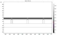
图5为现有技术中的超声波传感器的压电膜层的电场分布图;5 is an electric field distribution diagram of a piezoelectric film layer of an ultrasonic sensor in the prior art;
图6为本申请实施例提供的超声波传感器的压电膜层的电场分布图;6 is an electric field distribution diagram of a piezoelectric film layer of an ultrasonic sensor provided by an embodiment of the present application;
图7为现有技术中的超声波传感器的压电膜层和其承载基板的应力分布图;7 is a stress distribution diagram of a piezoelectric film layer of an ultrasonic sensor in the prior art and its carrying substrate;
图8为本申请实施例提供的超声波传感器的压电膜层和其承载基板的应力分布图;FIG. 8 is a stress distribution diagram of the piezoelectric film layer of the ultrasonic sensor and its carrying substrate provided by the embodiment of the application;
图9为本申请实施例提供的多个发射电极的俯视图;FIG. 9 is a top view of a plurality of emitter electrodes provided by an embodiment of the present application;
图10为本申请实施例提供的超声波传感器的一种结构示意图;10 is a schematic structural diagram of an ultrasonic sensor provided by an embodiment of the application;
图11为本申请实施例提供的超声波传感器的一种结构示意图;11 is a schematic structural diagram of an ultrasonic sensor provided by an embodiment of the application;
图12为本申请实施例提供的超声波传感器的一种结构示意图;12 is a schematic structural diagram of an ultrasonic sensor provided by an embodiment of the application;
图13为本申请实施例提供的超声波传感器的一种结构示意图;13 is a schematic structural diagram of an ultrasonic sensor provided by an embodiment of the application;
图14为本申请实施例提供的显示面板的一种结构示意图;FIG. 14 is a schematic structural diagram of a display panel provided by an embodiment of the present application;
图15为本申请实施例提供的显示面板的一种结构示意图;FIG. 15 is a schematic structural diagram of a display panel provided by an embodiment of the present application;
图16为本申请实施例提供的超声波传感器的制作方法的流程图。FIG. 16 is a flowchart of a method for fabricating an ultrasonic sensor provided by an embodiment of the present application.
具体实施方式Detailed ways
为使本发明的目的、技术方案和优点更加清楚明白,下面将结合本申请实施例中的附图,对本申请实施例中的技术方案进行清楚、完整地描述。In order to make the objectives, technical solutions and advantages of the present invention clearer, the technical solutions in the embodiments of the present application will be described clearly and completely below with reference to the accompanying drawings in the embodiments of the present application.
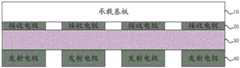
目前的超声波指纹识别技术中,超声波传感器的发射电极通常是整面设置,而传感器的接收电极是图案化设计。通常为了能够同时进行多路信息传输,发射电极和接收电极同时进行信号的收发,由于发射波是面状的,所以部分发射波有可能反射到与之对应的接收电极的相邻接收电极上,如图1所示。图1以超声波传感器具有4个接收电极,这4个接收电极分别为接收电极1、接收电极2、接收电极3和接收电极4为例。图1以接收电极2与其在承载基板上正投影重合的区域为限定的像素换能器(图1中以虚线进行示意)向发射电极发送1束发射波(图1中以箭头进行示意,箭头表示向多个方向发出的多条声波)为例,该发射波是一束波束角不为0度的波束,其中与垂直方向夹角分别为α和β的声波会分别反射到接收电极1和接收电极3,这样就会导致信号在相邻的接收电极之间发生串扰,进而导致传感器的信号接收量较低,对超声信号的利用率低,影响指纹识别的质量。In the current ultrasonic fingerprint recognition technology, the transmitting electrode of the ultrasonic sensor is usually set on the whole surface, while the receiving electrode of the sensor is a patterned design. Usually, in order to carry out multi-channel information transmission at the same time, the transmitting electrode and the receiving electrode transmit and receive signals at the same time. Since the transmitting wave is planar, part of the transmitting wave may be reflected on the adjacent receiving electrode of the corresponding receiving electrode. As shown in Figure 1. FIG. 1 takes the ultrasonic sensor having 4 receiving electrodes as an example, and the 4 receiving electrodes are respectively receiving
鉴于此,本申请实施例提供了一种新的超声波传感器,其发射电极也是图案化设计,一个接收电极与一个发射电极相对应,用于避免信号在相邻的接收电极之间可能发生的串扰,提高了超声波传感器的信号接收量。In view of this, the embodiment of the present application provides a new ultrasonic sensor, whose transmitting electrodes are also patterned, and one receiving electrode corresponds to one transmitting electrode, so as to avoid possible signal crosstalk between adjacent receiving electrodes. , which improves the signal reception of the ultrasonic sensor.
下面结合附图,对本发明实施例提供的超声波传感器及其制作方法和显示面板的具体实施方式进行详细地说明。附图中各膜层的厚度和形状不反映真实比例,目的只是示意说明本发明内容。The specific implementations of the ultrasonic sensor, its manufacturing method, and the display panel provided by the embodiments of the present invention will be described in detail below with reference to the accompanying drawings. The thickness and shape of each film layer in the drawings do not reflect the actual scale, and are only intended to illustrate the content of the present invention.
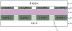
请参见图2,本发明实施例提供的一种超声波传感器,该超声波传感器包括承载基板10,以及在承载基板10上阵列设置的多个接收电极20、位于多个接收电极20上的压电膜层30,以及位于压电膜层30上且与多个接收电极20相对设置的多个发射电极40,一个接收电极20对应一个发射电极40;其中,任意一个发射电极40与相对的接收电极20在承载基板10的正投影具有重叠区域,且与相对的接收电极20周围的接收电极20在承载基板10的正投影互不交叠。Referring to FIG. 2 , an ultrasonic sensor provided by an embodiment of the present invention includes a
在一些实施例中,任意一个发射电极40与相对的接收电极20在承载基板10的正投影,可能有以下几种情况:In some embodiments, the orthographic projection of any one of the transmitting
第一种情况:任意一个接收电极20在承载基板10的正投影与相对的发射电极40在承载基板10的正投影相互重合,如图2所示。The first case: the orthographic projection of any one of the receiving
第二种情况:任意一个发射电极40在承载基板10的正投影完全覆盖相对的接收电极20在承载基板10的正投影,如图3所示。The second case: the orthographic projection of any one of the transmitting
第三种情况:任意一个接收电极20在承载基板10的正投影完全覆盖相对的发射电极40在承载基板10的正投影,如图4所示。The third situation: the orthographic projection of any one of the receiving
上述三种情况中任意一种情况都可以使得任意一个发射电极40与相对的接收电极20在承载基板10的正投影具有重叠区域,且与相对的接收电极20周围的接收电极20在承载基板10的正投影互不交叠,这样即使发射电极40和接收电极20同时进行信号的收发,接收电极20的发射波也不会发射到与之对应的接收电极20的相邻接收电极20上,从而避免了信号在相邻的接收电极20之间可能发生串扰的问题,提高了超声波传感器的信号接收量。In any of the above three situations, any one of the transmitting
为了便于理解,请参见图5,为现有技术中的超声波传感器的压电膜层30的电场分布图,以及请参见图6,为本申请实施例提供的超声波传感器的压电膜层30的电场分布图。其中,图5和图6均是发射电极40和接收电极20间加1V的交流电压下的电场分布图,图5和图6中不同深度的颜色分别表示不同的电场强度。For easy understanding, please refer to FIG. 5 , which is an electric field distribution diagram of the
对比图5和图6可以看出,图6中,图案化的发射电极40产生的交变电场相较于整面的发射电极40产生的交变电场更加集中在每个接收电极20的有效区域,从而减小了相邻接收电极20相互之间的电场耦合,即抑制了信号串扰,同时,提高了机电转换效率。Comparing FIGS. 5 and 6 , it can be seen that in FIG. 6 , the alternating electric field generated by the
另外,请参见图7,为现有技术中的超声波传感器的压电膜层和其承载基板的应力分布图,以及请参见图8,为本申请实施例提供的超声波传感器的压电膜层30和其承载基板10的应力分布图。从图7中可以看出,相邻像素换能器间传出的应力没有明显的界限,从而相邻像素换能器间会产生较大的串扰。而如图8所示,相邻像素换能器间传出的应力保持清晰的界限,从而会大大减小来自相邻像素换能器的串扰。In addition, please refer to FIG. 7 , which is a stress distribution diagram of a piezoelectric film layer of an ultrasonic sensor in the prior art and its supporting substrate, and please refer to FIG. 8 , which is a
且,根据信噪比公式(SNR=10logS/N)可以知道噪声信号功率越小,信噪比越大,其中,SNR表示信噪比,S表示有用信号的功率,N表示噪声信号的功率。在目前的超声波传感器中,接收电极20的噪声信号功率一部分来自串扰信号功率,一部分来自其他噪声信号功率,而本申请实施例避免信号在相邻的接收电极20之间发生串扰,所以降低了接收电极20的噪声信号功率,从而降低了总的噪声信号功率,提高了信噪比。Moreover, according to the signal-to-noise ratio formula (SNR=10logS/N), it can be known that the smaller the power of the noise signal, the greater the signal-to-noise ratio, where SNR represents the signal-to-noise ratio, S represents the power of the useful signal, and N represents the power of the noise signal. In the current ultrasonic sensor, part of the noise signal power of the receiving
由于发射电极40会对发射总电压进行分压,所以实际加载到压电膜层30上的电压小于该发射总电压,这样就会影响发射效率。发射电极40的电阻越低,实际加载到压电膜层30上的电压越高,从而发射电极40对信号的发射效率越高。由于发射电极40是整面时,发射电极40的电阻最小,而为了保证较高的发射效率,通常发射电极40是整面的。但是整面的发射电极40会产生信号串扰的问题,因此,本申请实施例采用图案化的发射电极40,即采用与例如氧化铟锡(ITO)制成的接收电极20一一对应的发射电极40,这样可能会使得发射电极40的电阻变大,不利于满足发射效率的需求。Since the
为此,请参见图9,为多个发射电极40的俯视图。本申请实施例中的每个发射电极40在承载基板10上的正投影为正方形,即每个发射电极40的形状为正方形。更进一步地相邻的两个发射电极40之间的连接构件41在承载基板10的正投影也为正方形。To this end, please refer to FIG. 9 , which is a top view of a plurality of
任意一个发射电极40的电阻可以通过公式(1)获得:The resistance of any one of the

在公式(1)中,R为发射电极40的电阻,L为发射电极40的长度,W为发射电极40的宽度,h为发射电极40的厚度,
从公式(1)中可以看出,当L与W相同时,发射电极40的电阻等于其方阻,所以本申请实施例中,每个发射电极40的形状为正方形,且相邻的两个发射电极40之间的连接构件41的形状也为正方形,可以使得发射电极40的电阻尽量小,以满足较高的发射效率。另外,每个发射电极40和连接构件41的形状均为正方形,也就是多个发射电极40形成的形状为正方形,可以保证超声波传感器横向分辨率和纵向分辨率相同,这样超声波成像效果不受待检测手指放置方向的影响,以尽量提高超声波传感器检测的精度。在一些实施例中,发射电极40的边长可以是60μm-70μm,相邻的发射电极40之间的间距小于待分辨的物体的尺寸,即相邻的发射电极40的连接构件41的边长可以是例如10μm-20μm。It can be seen from formula (1) that when L and W are the same, the resistance of the
请参见图10,本申请实施例提供的超声波传感器在位于多个发射电极40远离多个接收电极20一侧还设置有保护层50,以对多个发射电极40进行密封保护,同时也减小多个发射电极40由于外力带来的振动。在可能的实现方式中,保护层50的材料可以是环氧树脂。其中,环氧树脂中可以掺杂钨、氧化钨、氧化铁、二氧化钛、二氧化硅、滑石粉等用于调节声衰减系数和声阻抗的材料。Referring to FIG. 10, the ultrasonic sensor provided by the embodiment of the present application is further provided with a
在一些实施例中,请参见图11,相邻的两个发射电极40之间还填充有第一介质材料,形成第一介质材料层60,以使得压电膜层30与所述多个发射电极40相邻的表面平坦。In some embodiments, referring to FIG. 11 , a first dielectric material is also filled between two
在一些实施例中,请参见图12,相邻的两个接收电极20之间可以填充第二介质材料,形成第二介质材料层70,以使得压电膜层30与多个接收电极20相邻的表面平坦。第二介质材料层70可以是环氧树脂层或者氮化硅SiNx。In some embodiments, referring to FIG. 12 , a second dielectric material may be filled between two
通常来说,如果超声波传感器设置在显示面板,那么接收电极20的一侧会承载显示面板的其他器件,为了平衡压电膜层30两侧的重量,通常发射电极40较厚。但是由于图案化的工艺限制,较厚的发射电极40不易图案化,这也是现有技术中采用整面发射电极40的原因。Generally speaking, if the ultrasonic sensor is arranged on the display panel, one side of the receiving
而本申请实施例可以增加保护层50的厚度以减小发射电极40的厚度,同样可以平衡压电膜层30两侧的重量。In the embodiment of the present application, the thickness of the
在一些实施例中,每个发射电极40沿超声传感器的厚度方向的厚度位于[3μm,30μm]范围内,或者,每个发射电极40沿超声传感器的厚度方向的厚度位于[3μm,20μm]范围内,以使得发射电极40的厚度较薄,易于实现图案化。In some embodiments, the thickness of each transmitting
当发射电极40的厚度较薄,例如发射电极40的厚度为3μm~8μm,那么基于图案化的工艺,可以直接对整面的发射电极40进行图案化处理获得图案化的发射电极40,工艺较为简单。When the thickness of the
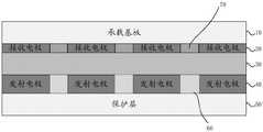
在一些实施例中,请参见图13,本发明实施例提供的超声波传感器在位于保护层50和多个发射电极40之间还设置有背衬电极层80,且在位于多个发射电极40和背衬电极层之间设置有绝缘层90。背衬电极层80和绝缘层90的设置可以减小发射电极40和/或保护层50的厚度。例如,每个发射电极40和背衬电极层80的总厚度沿超声传感器的厚度方向的厚度可以位于[10μm,20μm]范围内。又例如,由于制作发射电极40的金属或者制作背衬电极层80的金属等不同,或者制作工艺的精度要求,每个发射电极40和背衬电极层80沿超声传感器的厚度方向的厚度可能更厚或者更薄。这里背衬电极层可以理解为是为了使得发射电极40较薄而增加的膜层,为了尽可能的利用该膜层,那么该膜层可以是背衬电极层80,这样可以作为其他器件的供电电极等。In some embodiments, referring to FIG. 13 , the ultrasonic sensor provided by the embodiments of the present invention is further provided with a
在一些实施例中,可能的实施方式中,绝缘层90可以是氮化硅SiN层,其厚度可以小于1μm,尽量不影响声波的震动,减小对超声波传感器工作的影响。In some embodiments, in a possible implementation, the insulating
下面介绍上述超声波传感器的工作原理。The working principle of the above ultrasonic sensor is described below.
当发射电极40和接收电极20输入电压时,压电膜层30会发生形变,即压电膜层30带动上下膜层一起振动,进而产生声波传递出去。以发射电极40发射声波为例,当手指置于超声波传感器的接收电极20一侧时,发射电极40发射声波到用户手指谷或者手指脊,由于手指谷和手指脊反射能量不同,这样手指谷和手指脊就通过不同信号反应出来。When the transmitting
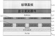
请参见图14,基于同一发明构思,本发明实施例还提供了一种显示面板,该显示面板包括显示背板,以及设置于显示背板上的如上述的超声波传感器;其中,承载基板10可以为显示背板的衬底基板,图14以此为例。例如该衬底基板可以是薄膜晶体管(Thin FilmTransistor,TFT)基板。承载基板10也可以不与显示背板共用衬底基板,这种情况下,承载基板10与显示背板的衬底基板粘合。当然,该显示面板还包括其他必须的器件,例如,显示发光器件100以及玻璃盖板200等,这里不再赘述。Referring to FIG. 14 , based on the same inventive concept, an embodiment of the present invention further provides a display panel, the display panel includes a display backplane, and the above-mentioned ultrasonic sensor disposed on the display backplane; wherein, the
在一些实施例中,承载基板10和显示发光器件100之间可以设置匹配层,该匹配层可以是声阻抗为承载基板10和显示发光器件100的声阻抗的几何平均值的材料。例如可以是掺杂钨、氧化钨、氧化铁、二氧化钛、二氧化硅、滑石粉等用于调节声阻抗的填料的环氧树脂。在可能的实施方式中,匹配层的厚度可以是超声波波长的四分之一,以尽量匹配承载基板10和显示发光器件100的声阻抗。In some embodiments, a matching layer may be disposed between the
请参见图15,在一些实施例中,承载基板10和接收电极20之间还设置有TFT像素电路。其中,TFT像素电路包括位于承载基板10上图案化的有源层(active),以及位于有源层上的栅极绝缘层(GI)和位于栅极绝缘层上的栅极(gate),以及设置在栅极绝缘层两侧的源极(S)和漏极(D)。具体的可以在承载基板10上制作多个接收电极20之前,可以在承载基板10上先制作TFT像素电路,再在TFT像素电路整面沉积氮化硅SiN、resin等介质层,之后在每个像素电路上对介质层进行开孔,然后沉积接收电极20,源极S通过开孔与接收电极20连接,从而实现了接收电极20与TFT像素电路之间的连接。Referring to FIG. 15 , in some embodiments, a TFT pixel circuit is further disposed between the
基于同一发明构思,本发明实施例还提供了一种上述超声波传感器的制作方法,如图16所示,该制作方法包括以下步骤:Based on the same inventive concept, an embodiment of the present invention also provides a method for manufacturing the above ultrasonic sensor, as shown in FIG. 16 , the manufacturing method includes the following steps:
S161、在承载基板10上制作阵列设置的多个接收电极20。S161 , fabricating a plurality of receiving
S162、在多个接收电极20上制作压电膜层30。S162 , forming piezoelectric film layers 30 on the plurality of receiving
S163、在压电膜层30上制作阵列设置的多个发射电极40。S163 , fabricating a plurality of
其中,在步骤S161中,承载基板10可以是玻璃、聚酰亚胺(PI)等。本申请实施例可以在承载基板10上采用喷墨打印方式制作一层金属层,再对金属层进行图案化处理,获得阵列排布的多个接收电极20。或者,在承载基板10上采用丝网印刷方式制作阵列排布的多个接收电极20。Wherein, in step S161, the
在步骤S162中,在多个接收电极20上沉积一层压电材料,形成压电膜层30。其中,该压电材料可以是由易于加工的高分子薄膜形成,例如,该压电材料可以是聚偏氟乙烯(PVDF)、聚偏二氟乙烯三氟乙烯(PVDF-TrFE)等。在具体制作时,压电膜层30的厚度可以位于5μm~15μm范围内。In step S162 , a layer of piezoelectric material is deposited on the plurality of receiving
由于压电膜层30和承载基板10之间的多个接收电极20是阵列排布的,也就是压电膜层30和承载基板10之间留有空气,而本申请实施例为了达到更好的超声波传播效率。在多个接收电极20上制作压电膜层30之前,可以在相邻的接收电极20之间填充第二介质材料70,可以使得压电膜层30与多个接收电极20相邻的表面平坦。Since the plurality of receiving
在步骤S163中,在压电膜层30上制作阵列设置的多个发射电极40可能包括以下两种制作方式。In step S163 , fabricating a plurality of
第一种制作方式:The first way to make:
先在压电膜层30上制作介质材料层60,再对介质材料层60进行图案化处理,形成多个与发射电极40层的互补图案,之后在图案化后的介质材料层60上制作发射电极40材料,形成多个发射电极40。First, a
例如,在压电膜层30上沉积一层例如厚度位于2μm~10μm范围内环氧树脂层,通过光刻刻蚀工艺将环氧树脂层图案化,以形成多个发射电极40层的互补图案。接着利用电镀工艺或喷墨打印技术沉积一层金属层,形成多个发射电极40。其中,这里的金属层包括但不限于Cu、Mo、Ag等声阻抗较大的金属。For example, an epoxy resin layer with a thickness ranging from 2 μm to 10 μm is deposited on the
根据声波反射率等于两层介质声阻抗之差比声阻抗之和,可知声波在声阻抗差异较大的两界面间的反射率较高,以将压电膜层30发射出的声波反射至检测对象方向。在一些实施例中,多个发射电极40的厚度与图案化的介质材料层60的厚度一致,以保证压电膜层30的发射率较高,同时压电膜层30与多个发射电极40相邻的表面平坦。According to the sound wave reflectivity equal to the difference between the acoustic impedances of the two layers of media and the sum of the acoustic impedances, it can be known that the acoustic wave has a higher reflectivity between the two interfaces with large acoustic impedance differences, so as to reflect the acoustic waves emitted by the
第二种制作方式:The second way to make:
先在压电膜层30上制作发射电极材料,再对发射电极40材料进行图案化处理,形成多个发射电极40。这样可以省去制作图案化的环氧树脂的步骤。First, the emitter electrode material is fabricated on the
这种制作方式下,考虑到对发射电极材料进行图案化处理,通常发射电极材料是金属,如果发射电极材料较厚,对图案化工艺要求较高,所以,在一些实施例中,发射电极材料的厚度较薄,例如发射电极材料的厚度可以小于4μm,对图案化工艺的要求较低,易于实现。In this manufacturing method, considering that the emitter electrode material is patterned, usually the emitter electrode material is metal. If the emitter electrode material is thick, the patterning process is required to be higher. Therefore, in some embodiments, the emitter electrode material is The thickness is relatively thin, for example, the thickness of the emitter electrode material can be less than 4 μm, which has lower requirements on the patterning process and is easy to implement.
不管是第一种制作方式,还是第二种制作方式考虑到图化的多个发射电极40裸露容易氧化,所以在制作多个发射电极40之后,可以在发射电极40之上制作保护层50,以保护发射电极40。Regardless of whether it is the first manufacturing method or the second manufacturing method, considering that the
具体的,如果是采用第一种制作方式制作多个发射电极40,那么可以在多个发射电极40上沉积一层环氧树脂层作为保护层50。如果是采用第二种制作方式制作多个发射电极40,可以先在相邻发射电极40之间填充介质材料60,再制作保护层50。其中,多个发射电极40的厚度与填充的介质材料60的厚度一致,以保证压电膜层30的发射率较高,同时压电膜层30与多个发射电极40相邻的表面平坦,同时,还可以减小发射电极40由外力引起的震动。或者,也可以采用热压固化方式涂覆一层环氧树脂层,且该环氧树脂层的部分填充在相邻发射电极40之间,既达到在相邻发射电极40之间填充介质材料的目的,又达到制作保护层50的目的,简化了工艺。Specifically, if
在一些实施例中,采用第二种制作方式制作发射电极40时,为了让发射电极40更薄,在相邻的两个发射电极40之间填充介质材料60之后,还可以在多个发射电极40上制作绝缘层90,之后再在所述绝缘层90上制作背衬电极层80,然后在背衬电极层80上制作保护层50。In some embodiments, when the
综上,本申请实施例的超声波传感器包括阵列设置的多个接收电极和多个发射电极,其中,任意一个发射电极与相对的接收电极在承载基板的正投影具有重叠区域,且与相对的接收电极周围的接收电极在承载基板的正投影互不交叠,这样即使发射电极和接收电极同时进行信号的收发,接收电极的发射波也不会发射到与之对应的接收电极的相邻接收电极上,从而避免了信号在相邻的接收电极之间可能发生串扰的问题,提高了超声波传感器的信号接收量。To sum up, the ultrasonic sensor according to the embodiment of the present application includes a plurality of receiving electrodes and a plurality of transmitting electrodes arranged in an array, wherein any one of the transmitting electrodes and the opposite receiving electrode has an overlapping area on the orthographic projection of the carrier substrate, and has an overlapping area with the opposite receiving electrode. The orthographic projections of the receiving electrodes around the electrodes do not overlap each other on the carrier substrate, so that even if the transmitting electrodes and the receiving electrodes transmit and receive signals at the same time, the transmitting waves of the receiving electrodes will not be transmitted to the adjacent receiving electrodes of the corresponding receiving electrodes. Therefore, the problem of possible crosstalk between adjacent receiving electrodes is avoided, and the signal receiving capacity of the ultrasonic sensor is improved.
显然,本领域的技术人员可以对本发明进行各种改动和变型而不脱离本发明的精神和范围。这样,倘若本发明的这些修改和变型属于本发明权利要求及其等同技术的范围之内,则本发明也意图包含这些改动和变型在内。It will be apparent to those skilled in the art that various modifications and variations can be made in the present invention without departing from the spirit and scope of the invention. Thus, provided that these modifications and variations of the present invention fall within the scope of the claims of the present invention and their equivalents, the present invention is also intended to include these modifications and variations.
Claims (16)
Priority Applications (1)
| Application Number | Priority Date | Filing Date | Title |
|---|---|---|---|
| CN201910402605.6ACN111950324B (en) | 2019-05-15 | 2019-05-15 | Ultrasonic sensor, manufacturing method thereof and display panel |
Applications Claiming Priority (1)
| Application Number | Priority Date | Filing Date | Title |
|---|---|---|---|
| CN201910402605.6ACN111950324B (en) | 2019-05-15 | 2019-05-15 | Ultrasonic sensor, manufacturing method thereof and display panel |
Publications (2)
| Publication Number | Publication Date |
|---|---|
| CN111950324Atrue CN111950324A (en) | 2020-11-17 |
| CN111950324B CN111950324B (en) | 2024-07-26 |
Family
ID=73336598
Family Applications (1)
| Application Number | Title | Priority Date | Filing Date |
|---|---|---|---|
| CN201910402605.6AActiveCN111950324B (en) | 2019-05-15 | 2019-05-15 | Ultrasonic sensor, manufacturing method thereof and display panel |
Country Status (1)
| Country | Link |
|---|---|
| CN (1) | CN111950324B (en) |
Cited By (3)
| Publication number | Priority date | Publication date | Assignee | Title |
|---|---|---|---|---|
| CN116713172A (en)* | 2023-06-13 | 2023-09-08 | 京东方科技集团股份有限公司 | Ultrasonic transducer substrate and production method and equipment thereof |
| WO2024093318A1 (en)* | 2022-10-31 | 2024-05-10 | 华为技术有限公司 | Ultrasonic transducer, fingerprint recognition module, and electronic device |
| WO2024240197A1 (en)* | 2023-05-23 | 2024-11-28 | 华为技术有限公司 | Transducer, transducing apparatus and terminal |
Citations (10)
| Publication number | Priority date | Publication date | Assignee | Title |
|---|---|---|---|---|
| CN105808026A (en)* | 2011-03-11 | 2016-07-27 | 创造者科技有限公司 | Two prong capacitive sensor pattern |
| CN106155450A (en)* | 2016-07-29 | 2016-11-23 | 厦门天马微电子有限公司 | Integrated touch-control display panel and display device |
| CN205880425U (en)* | 2016-08-09 | 2017-01-11 | 厦门天马微电子有限公司 | Display panel and display apparatus |
| US20170110504A1 (en)* | 2015-10-14 | 2017-04-20 | Qualcomm Incorporated | Integrated piezoelectric micromechanical ultrasonic transducer pixel and array |
| CN106951130A (en)* | 2017-03-28 | 2017-07-14 | 京东方科技集团股份有限公司 | A kind of array base palte, display panel, display device and array base palte preparation method |
| CN107491211A (en)* | 2017-08-28 | 2017-12-19 | 上海中航光电子有限公司 | A kind of touch-control display panel and touch control display apparatus |
| CN108446685A (en)* | 2018-05-24 | 2018-08-24 | 京东方科技集团股份有限公司 | Ultrasonic fingerprint identifies module and preparation method thereof and display device |
| CN109492470A (en)* | 2017-09-12 | 2019-03-19 | 南昌欧菲生物识别技术有限公司 | Ultrasonic sensor and electronic device |
| CN109491550A (en)* | 2019-01-03 | 2019-03-19 | 京东方科技集团股份有限公司 | A kind of touch base plate and its detection method, display device |
| US20190129019A1 (en)* | 2017-10-26 | 2019-05-02 | Seiko Epson Corporation | Ultrasonic Device And Ultrasonic Measuring Apparatus |
- 2019
- 2019-05-15CNCN201910402605.6Apatent/CN111950324B/enactiveActive
Patent Citations (10)
| Publication number | Priority date | Publication date | Assignee | Title |
|---|---|---|---|---|
| CN105808026A (en)* | 2011-03-11 | 2016-07-27 | 创造者科技有限公司 | Two prong capacitive sensor pattern |
| US20170110504A1 (en)* | 2015-10-14 | 2017-04-20 | Qualcomm Incorporated | Integrated piezoelectric micromechanical ultrasonic transducer pixel and array |
| CN106155450A (en)* | 2016-07-29 | 2016-11-23 | 厦门天马微电子有限公司 | Integrated touch-control display panel and display device |
| CN205880425U (en)* | 2016-08-09 | 2017-01-11 | 厦门天马微电子有限公司 | Display panel and display apparatus |
| CN106951130A (en)* | 2017-03-28 | 2017-07-14 | 京东方科技集团股份有限公司 | A kind of array base palte, display panel, display device and array base palte preparation method |
| CN107491211A (en)* | 2017-08-28 | 2017-12-19 | 上海中航光电子有限公司 | A kind of touch-control display panel and touch control display apparatus |
| CN109492470A (en)* | 2017-09-12 | 2019-03-19 | 南昌欧菲生物识别技术有限公司 | Ultrasonic sensor and electronic device |
| US20190129019A1 (en)* | 2017-10-26 | 2019-05-02 | Seiko Epson Corporation | Ultrasonic Device And Ultrasonic Measuring Apparatus |
| CN108446685A (en)* | 2018-05-24 | 2018-08-24 | 京东方科技集团股份有限公司 | Ultrasonic fingerprint identifies module and preparation method thereof and display device |
| CN109491550A (en)* | 2019-01-03 | 2019-03-19 | 京东方科技集团股份有限公司 | A kind of touch base plate and its detection method, display device |
Cited By (5)
| Publication number | Priority date | Publication date | Assignee | Title |
|---|---|---|---|---|
| WO2024093318A1 (en)* | 2022-10-31 | 2024-05-10 | 华为技术有限公司 | Ultrasonic transducer, fingerprint recognition module, and electronic device |
| EP4509230A4 (en)* | 2022-10-31 | 2025-09-03 | Huawei Tech Co Ltd | ULTRASONIC TRANSDUCER, FINGERPRINT RECOGNITION MODULE, AND ELECTRONIC DEVICE |
| WO2024240197A1 (en)* | 2023-05-23 | 2024-11-28 | 华为技术有限公司 | Transducer, transducing apparatus and terminal |
| CN116713172A (en)* | 2023-06-13 | 2023-09-08 | 京东方科技集团股份有限公司 | Ultrasonic transducer substrate and production method and equipment thereof |
| WO2024255507A1 (en)* | 2023-06-13 | 2024-12-19 | 京东方科技集团股份有限公司 | Ultrasonic transducer substrate and manufacturing method therefor, and device |
Also Published As
| Publication number | Publication date |
|---|---|
| CN111950324B (en) | 2024-07-26 |
Similar Documents
| Publication | Publication Date | Title |
|---|---|---|
| CN111758099B (en) | Fingerprint identification module, driving method and manufacturing method thereof and display device | |
| US11120243B2 (en) | Fingerprint identification module, manufacturing method and driving method thereof, display device | |
| CN110265457B (en) | Organic light-emitting display panel and preparation method | |
| CN108446685B (en) | Ultrasonic fingerprint identification module, preparation method thereof and display device | |
| CN110265544A (en) | Piezoelectric sensor and preparation method, fingerprint recognition method and electronic device | |
| CN109948496B (en) | Fingerprint identification device and display device | |
| CN111950324B (en) | Ultrasonic sensor, manufacturing method thereof and display panel | |
| CN110275577B (en) | Ultrasound module and display | |
| CN111782090B (en) | Display module, ultrasonic touch detection method and ultrasonic fingerprint identification method | |
| CN111695388B (en) | Fingerprint recognition structure and driving method thereof, and display device | |
| CN107403129A (en) | Ultrasonic fingerprint identification module, ultrasonic fingerprint recognition means and electronic equipment | |
| CN110276325A (en) | Ultrasonic fingerprint identification component, ultrasonic fingerprint identification device and display device | |
| CN102194991A (en) | Piezoelectric element, piezoelectric sensor, electronic device, and method for manufacturing piezoelectric element | |
| CN102988079A (en) | Ultrasonic probe and ultrasonic image diagnostic device | |
| CN115971021B (en) | Ultrasonic transduction substrate, manufacturing method of transduction substrate and detection method | |
| CN110764641A (en) | Display panel and display device | |
| TWI621982B (en) | Fingerprint identification device, manufacturing method thereof and display device | |
| US11703478B2 (en) | Micro total analysis system, operating method and manufacturing method thereof | |
| CN109492474A (en) | Ultrasonic fingerprint identifies mould group and electronic equipment | |
| WO2020232934A1 (en) | Display panel structure and electronic device | |
| CN207182304U (en) | Electronic equipment | |
| CN111242095A (en) | An ultrasonic pattern recognition module, a preparation method thereof, and a display device | |
| CN206849038U (en) | Ultrasonic fingerprint identification module, ultrasonic fingerprint recognition means and electronic equipment | |
| CN111652109A (en) | Electronic equipment | |
| TWI879528B (en) | Ultrasonic transducer |
Legal Events
| Date | Code | Title | Description |
|---|---|---|---|
| PB01 | Publication | ||
| PB01 | Publication | ||
| SE01 | Entry into force of request for substantive examination | ||
| SE01 | Entry into force of request for substantive examination | ||
| GR01 | Patent grant | ||
| GR01 | Patent grant | ||
| TG01 | Patent term adjustment | ||
| TG01 | Patent term adjustment |