CN111948220A - Chip testing equipment - Google Patents
Chip testing equipmentDownload PDFInfo
- Publication number
- CN111948220A CN111948220ACN202010956644.3ACN202010956644ACN111948220ACN 111948220 ACN111948220 ACN 111948220ACN 202010956644 ACN202010956644 ACN 202010956644ACN 111948220 ACN111948220 ACN 111948220A
- Authority
- CN
- China
- Prior art keywords
- clamping
- chip
- clamping jaw
- clamping mechanism
- rail structure
- Prior art date
- Legal status (The legal status is an assumption and is not a legal conclusion. Google has not performed a legal analysis and makes no representation as to the accuracy of the status listed.)
- Granted
Links
Images


Classifications
- G—PHYSICS
- G01—MEASURING; TESTING
- G01N—INVESTIGATING OR ANALYSING MATERIALS BY DETERMINING THEIR CHEMICAL OR PHYSICAL PROPERTIES
- G01N21/00—Investigating or analysing materials by the use of optical means, i.e. using sub-millimetre waves, infrared, visible or ultraviolet light
- G01N21/84—Systems specially adapted for particular applications
- G01N21/88—Investigating the presence of flaws or contamination
- G01N21/89—Investigating the presence of flaws or contamination in moving material, e.g. running paper or textiles
- G01N21/892—Investigating the presence of flaws or contamination in moving material, e.g. running paper or textiles characterised by the flaw, defect or object feature examined
Landscapes
- Engineering & Computer Science (AREA)
- Textile Engineering (AREA)
- Physics & Mathematics (AREA)
- Health & Medical Sciences (AREA)
- Life Sciences & Earth Sciences (AREA)
- Chemical & Material Sciences (AREA)
- Analytical Chemistry (AREA)
- Biochemistry (AREA)
- General Health & Medical Sciences (AREA)
- General Physics & Mathematics (AREA)
- Immunology (AREA)
- Pathology (AREA)
- Specific Conveyance Elements (AREA)
- Testing Of Individual Semiconductor Devices (AREA)
Abstract
Translated fromChinese
Description
Translated fromChinese技术领域technical field
本发明涉及芯片检测技术领域,尤其是涉及一种芯片检测设备。The invention relates to the technical field of chip detection, in particular to a chip detection device.
背景技术Background technique
芯片在加工时会进行一系列的检查,从而检测出一些缺陷。对缺陷进行处理,可以避免材料的浪费,以及废品的产生。Chips are processed through a series of inspections to detect defects. Dealing with defects can avoid wastage of materials and the generation of waste products.
现有的芯片检测方法采用人工筛选,操作人员将芯片载板从弹夹中取出,利用显微镜对每个芯片进行观察,对缺陷进行逐一检测,将符合要求的产品留下,将不符合要求的产品返回到相应的工位进行重新加工。The existing chip detection method adopts manual screening. The operator takes out the chip carrier from the magazine, observes each chip with a microscope, detects the defects one by one, and leaves the products that meet the requirements, and those that do not meet the requirements are left The product is returned to the corresponding station for reprocessing.
由于人工检测的随机性与不确定性,没有办法确保把所有的缺陷都检测出来,并且,人工无法确保所有的芯片保质保量的进行检测,容易出现漏检或未检的情况发生;并且,人工检测需要操作人员手工进行上、下料,这个过程非常容易对芯片造成污染,导致检测质量和检测效率低的问题。Due to the randomness and uncertainty of manual testing, there is no way to ensure that all defects are detected, and manual testing cannot ensure the quality and quantity of all chips, which is prone to missed or unchecked inspections; and, Manual testing requires operators to manually load and unload materials. This process is very easy to contaminate the chip, resulting in low testing quality and testing efficiency.
发明内容SUMMARY OF THE INVENTION
本发明的目的在于提供一种芯片检测设备,以缓解人工检测没有办法确保把所有的缺陷都检测出来,并且,人工无法确保所有的芯片保质保量的进行检测,容易出现漏检或未检的情况发生;并且,人工检测需要操作人员手工进行上、下料,这个过程非常容易对芯片造成污染,导致检测质量和检测效率低的问题。The purpose of the present invention is to provide a chip inspection device, so as to alleviate the inability of manual inspection to ensure that all defects are detected, and manual inspection cannot ensure the quality and quantity of all chips to be inspected, which is prone to missed inspection or uninspected inspection. In addition, manual inspection requires operators to manually load and unload materials, which is very easy to contaminate the chip, resulting in low inspection quality and inspection efficiency.
本发明实施例提供的一种芯片检测设备,所述芯片检测设备包括:滑轨结构、抽取装置、运输装置和图像采集检测装置;An embodiment of the present invention provides a chip detection device, the chip detection device includes: a slide rail structure, an extraction device, a transportation device, and an image acquisition and detection device;
所述抽取装置用于将弹夹内的芯片载板抽出并放置在滑轨结构上;The extraction device is used for pulling out the chip carrier in the magazine and placing it on the slide rail structure;
所述运输装置用于将所述滑轨结构上的芯片载板运输到检测位置,或者将检测位置的芯片载板从检测位置移出;The transport device is used to transport the chip carrier on the slide rail structure to the detection position, or to move the chip carrier at the detection position from the detection position;
所述图像采集检测装置位于所述检测位置的上方,用于采集芯片载板上芯片的图像,并将所述图像与标准图像进行比较,从而获取芯片载板上芯片的缺陷。The image acquisition and detection device is located above the detection position, and is used for acquiring the image of the chip on the chip carrier, and comparing the image with the standard image, so as to obtain the defects of the chip on the chip carrier.
进一步的,所述图像采集检测装置包括移动平台、图像采集机构和环形光源;Further, the image acquisition and detection device includes a mobile platform, an image acquisition mechanism and a ring light source;
所述移动平台能够带动所述图像采集机构沿第一方向和第二方向运动,所述第一方向和第二方向所成的面与滑轨结构的长度方向垂直;The moving platform can drive the image acquisition mechanism to move along a first direction and a second direction, and the surface formed by the first direction and the second direction is perpendicular to the length direction of the slide rail structure;
所述环形光源连接在所述图像采集机构的最下端,且所述环形光源的圆心与所述图像采集机构的光轴同轴。The ring light source is connected to the lowermost end of the image acquisition mechanism, and the center of the ring light source is coaxial with the optical axis of the image acquisition mechanism.
进一步的,所述抽取装置包括左右输送机构和第一夹持机构;Further, the extraction device includes a left and right conveying mechanism and a first clamping mechanism;
所述左右输送机构包括运输底座和线性驱动模组,所述线性驱动模组用于驱动所述运输底座沿滑轨结构的长度方向运动;所述第一夹持机构位于所述运输底座上,所述第一夹持机构用于夹住弹夹内的芯片载板。The left and right conveying mechanisms include a transport base and a linear drive module, the linear drive module is used to drive the transport base to move along the length direction of the slide rail structure; the first clamping mechanism is located on the transport base, The first clamping mechanism is used for clamping the chip carrier in the magazine.
进一步的,所述滑轨结构包括平行且间隔的两道导轨,所述第一夹持机构位于所述滑轨结构的下方;Further, the slide rail structure includes two parallel and spaced guide rails, and the first clamping mechanism is located below the slide rail structure;
所述第一夹持机构与所述运输底座活动连接,所述抽取装置包括第一竖向驱动机构,所述第一竖向驱动机构用于带动所述第一夹持机构在竖向上运动。The first clamping mechanism is movably connected with the transport base, and the extraction device includes a first vertical driving mechanism, and the first vertical driving mechanism is used to drive the first clamping mechanism to move vertically.
进一步的,所述运输底座与所述第一夹持机构通过连接件连接,所述连接件的一端与所述运输底座铰接,所述连接件的另一端与所述第一夹持机构铰接;Further, the transport base is connected with the first clamping mechanism through a connecting piece, one end of the connecting piece is hinged with the transport base, and the other end of the connecting piece is hinged with the first clamping mechanism;
所述第一竖向驱动机构包括压缩弹簧,所述压缩弹簧的一端与所述连接件连接,所述压缩弹簧的另一端与所述运输底座连接,所述压缩弹簧用于使所述第一夹持机构具有向上运动的趋势;The first vertical drive mechanism includes a compression spring, one end of the compression spring is connected with the connecting piece, the other end of the compression spring is connected with the transport base, and the compression spring is used to make the first The clamping mechanism has a tendency to move upward;
所述连接件上设置有止挡块,所述止挡块与所述导轨的底面抵接;所述导轨的底面上设置有导向凸台,所述导向凸台朝向所述导轨首端的面为斜面,自所述导轨的首端向尾端方向,所述斜面向下倾斜,所述斜面用于引导所述止挡块向上或者向下运动,以使所述第一夹持机构上升或者下降。A stop block is arranged on the connecting piece, and the stop block is in contact with the bottom surface of the guide rail; a guide boss is arranged on the bottom surface of the guide rail, and the surface of the guide boss facing the head end of the guide rail is: an inclined surface, from the head end to the tail end of the guide rail, the inclined surface is inclined downward, and the inclined surface is used to guide the stop block to move upward or downward, so as to make the first clamping mechanism rise or fall .
进一步的,所述线性驱动模组包括第一左右伸缩模组和第二左右伸缩模组;所述运输底座上滑动连接有滑块,所述滑块的滑动方向与所述滑轨结构的长度方向相同,所述第一夹持机构和第二左右伸缩模组固定在所述滑块上;Further, the linear drive module includes a first left and right telescopic module and a second left and right telescopic module; a sliding block is slidably connected to the transport base, and the sliding direction of the sliding block is the same as the length of the sliding rail structure. The directions are the same, and the first clamping mechanism and the second left and right telescopic modules are fixed on the slider;
所述第一左右伸缩模组与所述运输底座连接,用于驱动所述运输底座、滑块和第一夹持机构沿横向运动,所述第二左右伸缩模组与所述滑块连接,用于驱动所述滑块和第一夹持机构沿横向运动。The first left and right telescopic modules are connected with the transport base, and are used to drive the transport base, the slider and the first clamping mechanism to move laterally, and the second left and right telescopic modules are connected with the slider, It is used to drive the slider and the first clamping mechanism to move laterally.
进一步的,所述第一夹持机构包括上端夹持爪、下端夹持爪和第一竖向驱动机构,所述第一竖向驱动机构的活动端与所述上端夹持爪连接,用于带动所述上端夹持爪朝向或者远离下端夹持爪运动;Further, the first clamping mechanism includes an upper clamping claw, a lower clamping claw and a first vertical driving mechanism, and the movable end of the first vertical driving mechanism is connected with the upper clamping claw for Drive the upper clamping claw to move toward or away from the lower clamping claw;
所述第一竖向驱动机构包括连接杆、磁铁、电磁铁,所述磁铁和电磁铁固定在所述下端夹持爪上,所述磁铁能够沿所述上端夹持爪和下端夹持爪的开合方向,朝向或者远离所述电磁铁运动;所述连接杆的一端与所述磁铁连接,另一端与所述上端夹持爪铰接。The first vertical drive mechanism includes a connecting rod, a magnet, and an electromagnet. The magnet and the electromagnet are fixed on the lower end clamping claw, and the magnet can move along the upper end clamping claw and the lower end clamping claw. The opening and closing direction moves toward or away from the electromagnet; one end of the connecting rod is connected with the magnet, and the other end is hinged with the upper clamping claw.
进一步的,所述滑轨结构包括平行且间隔的两道导轨,所述运输装置还包括第二夹持机构和左右驱动机构,所述左右驱动机构用于带动所述第二夹持机构沿与所述导轨平行的方向运动;Further, the slide rail structure includes two parallel and spaced guide rails, and the transport device further includes a second clamping mechanism and a left and right driving mechanism, and the left and right driving mechanisms are used to drive the second clamping mechanism along the The guide rails move in parallel directions;
至少一个所述导轨的侧面设置有第二夹持机构,所述第二夹持机构包括能够开合的第一夹爪和第二夹爪,以及第二竖向驱动机构;所述第二夹爪包括位于两道导轨之间的第二夹持边沿;所述第一夹爪包括滑槽,所述滑槽的扣在所述导轨上,且所述滑槽包括间隔设置的两个槽壁,位于两道所述导轨之间的槽壁与所述第二夹持边沿对齐以形成第一夹持边沿;所述第二竖向驱动机构用于驱动所述第一夹爪和第二夹爪开合。At least one side of the guide rail is provided with a second clamping mechanism, the second clamping mechanism includes a first clamping claw and a second clamping claw that can be opened and closed, and a second vertical driving mechanism; the second clamping mechanism The claw includes a second clamping edge located between the two guide rails; the first clamping claw includes a chute, the chute is fastened on the guide rail, and the chute includes two groove walls arranged at intervals , the groove wall between the two guide rails is aligned with the second clamping edge to form a first clamping edge; the second vertical driving mechanism is used to drive the first clamping jaw and the second clamping edge Claws open and close.
进一步的,所述第二竖向驱动机构包括伸缩缸、第一安装座、滑动块,连接臂、第二安装座、联动齿轮;Further, the second vertical drive mechanism includes a telescopic cylinder, a first mounting seat, a sliding block, a connecting arm, a second mounting seat, and a linkage gear;
沿所述第一夹爪和第二夹爪的开合方向,所述滑动块与所述第一安装座滑动连接,所述第一夹爪与所述滑动块连接,所述连接臂的一端与所述滑动块连接,所述连接臂的另一端设置有第一齿条部,所述第一齿条部与所述联动齿轮啮合;Along the opening and closing directions of the first clamping jaw and the second clamping jaw, the sliding block is slidably connected with the first mounting seat, the first clamping jaw is connected with the sliding block, and one end of the connecting arm is connected with the sliding block, the other end of the connecting arm is provided with a first rack portion, and the first rack portion is engaged with the linkage gear;
所述联动齿轮转动连接在所述第二安装座上,所述第二夹爪的侧壁上设置有第二齿条部,所述第二齿条部与所述联动齿轮啮合,且所述第一齿条部和第二齿条部分别位于所述联动齿轮的相对两侧;沿所述第一夹爪和第二夹爪的开合方向,所述第二夹爪与所述第二安装座滑动连接;The linkage gear is rotatably connected to the second mounting seat, a second rack portion is provided on the side wall of the second jaw, the second rack portion is engaged with the linkage gear, and the The first rack portion and the second rack portion are respectively located on opposite sides of the interlocking gear; along the opening and closing directions of the first jaw and the second jaw, the second jaw and the second jaw Mounting seat sliding connection;
所述伸缩缸固定在所述第一安装座上,所述伸缩缸的活动端与所述连接臂连接,用于带动所述连接臂沿所述第一夹爪和第二夹爪的开合方向运动。The telescopic cylinder is fixed on the first mounting seat, and the movable end of the telescopic cylinder is connected with the connecting arm for driving the connecting arm to open and close along the first and second clamping jaws directional movement.
进一步的,所述滑轨结构上还具有初始位置和出料位置,所述初始位置的末端设置有第一接近开关,所述检测位置的末端设置第二接近开关,所述出料位置的位置设置有第三接近开关,所述第一接近开关、第二接近开关和第三接近开关均与所述左右驱动机构电连接。Further, the slide rail structure also has an initial position and a discharge position, the end of the initial position is provided with a first proximity switch, the end of the detection position is provided with a second proximity switch, and the position of the discharge position is provided. A third proximity switch is provided, and the first proximity switch, the second proximity switch and the third proximity switch are all electrically connected to the left and right driving mechanisms.
本发明实施例提供的所述芯片检测设备包括:滑轨结构、抽取装置、运输装置和图像采集检测装置;所述抽取装置用于将弹夹内的芯片载板抽出并放置在滑轨结构上;所述运输装置用于将所述滑轨结构上的芯片载板运输到检测位置,或者将检测位置的芯片载板从检测位置移出;所述图像采集检测装置位于所述检测位置的上方,用于采集芯片载板上芯片的图像,并将所述图像与标准图像进行比较,从而获取芯片载板上芯片的缺陷。可以先将弹夹与滑轨结构的首端对齐,然后利用抽取装置从弹夹中将芯片载板抽出,并放置在滑轨结构上;然后,利用运输装置向前移动芯片载板,从而使芯片载板运动到图像采集检测装置下方的检测位置,利用图像采集监测装置采集芯片的图像,将采集到的图像与系统里预存的标准图像进行对比,从而可以得到被检测芯片存在缺陷的位置,检测完的芯片将会被运输装置继续向前运输,从而离开检测位置。然后运输装置再将下一个芯片载板运输到检测位置进行检测。在抽取、运输和检测的过程中,均没有人为的参与,降低了人为污染芯片的风险,利用机械代替人工,可以提高检测的效率和质量。The chip detection device provided by the embodiment of the present invention includes: a slide rail structure, an extraction device, a transportation device, and an image acquisition and detection device; the extraction device is used to extract the chip carrier in the magazine and place it on the slide rail structure ; the transport device is used to transport the chip carrier on the slide rail structure to the detection position, or move the chip carrier in the detection position from the detection position; the image acquisition detection device is located above the detection position, It is used to collect the image of the chip on the chip carrier, and compare the image with the standard image, so as to obtain the defects of the chip on the chip carrier. You can first align the clip with the head end of the slide rail structure, and then use the extraction device to pull out the chip carrier from the clip and place it on the slide rail structure; then, use the transport device to move the chip carrier forward, so that the The chip carrier moves to the detection position under the image acquisition and detection device, and the image acquisition and monitoring device is used to acquire the image of the chip, and the acquired image is compared with the standard image pre-stored in the system, so as to obtain the defect position of the detected chip. The detected chips will be transported forward by the transport device, thereby leaving the detection position. Then the transport device transports the next chip carrier to the detection position for detection. In the process of extraction, transportation and testing, there is no human participation, which reduces the risk of artificial contamination of the chip, and the use of machinery instead of labor can improve the efficiency and quality of testing.
附图说明Description of drawings
为了更清楚地说明本发明具体实施方式或现有技术中的技术方案,下面将对具体实施方式或现有技术描述中所需要使用的附图作简单地介绍,显而易见地,下面描述中的附图是本发明的一些实施方式,对于本领域普通技术人员来讲,在不付出创造性劳动的前提下,还可以根据这些附图获得其他的附图。In order to more clearly illustrate the specific embodiments of the present invention or the technical solutions in the prior art, the following briefly introduces the accompanying drawings required in the description of the specific embodiments or the prior art. Obviously, the accompanying drawings in the following description The drawings are some embodiments of the present invention. For those of ordinary skill in the art, other drawings can also be obtained from these drawings without creative efforts.
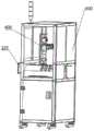
图1为本发明实施例提供的芯片检测设备的示意图;1 is a schematic diagram of a chip detection device provided by an embodiment of the present invention;
图2为本发明实施例提供的芯片检测设备的示意图(去除壳体);2 is a schematic diagram of a chip detection device provided by an embodiment of the present invention (with the casing removed);
图3为本发明实施例提供的芯片检测设备的抽取装置的示意图;3 is a schematic diagram of an extraction device of a chip detection device provided by an embodiment of the present invention;
图4为本发明实施例提供的芯片检测设备的抽取装置的正视图;4 is a front view of an extraction device of a chip detection device provided by an embodiment of the present invention;
图5为本发明实施例提供的芯片检测设备的抽取装置的俯视图;5 is a top view of an extraction device of a chip detection device provided by an embodiment of the present invention;
图6为图5中A-A方向的剖视图;Fig. 6 is the sectional view of A-A direction in Fig. 5;
图7为图6中B位置的局部放大图;Fig. 7 is a partial enlarged view of position B in Fig. 6;
图8为本发明实施例提供的芯片检测设备的夹取机构的示意图;8 is a schematic diagram of a clamping mechanism of a chip detection device provided by an embodiment of the present invention;
图9为本发明实施例提供的芯片检测设备的芯片载板传输装置的俯视图;FIG. 9 is a top view of a chip carrier transfer device of a chip detection device provided by an embodiment of the present invention;
图10为本发明实施例提供的芯片检测设备的第二夹持机构的示意图;FIG. 10 is a schematic diagram of a second clamping mechanism of a chip detection device provided by an embodiment of the present invention;
图11为本发明实施例提供的芯片检测设备的第二夹持机构的正视图;11 is a front view of the second clamping mechanism of the chip detection device provided by the embodiment of the present invention;
图12为本发明实施例提供的芯片检测设备的第二夹持机构的侧视图。FIG. 12 is a side view of the second clamping mechanism of the chip detection device provided by the embodiment of the present invention.
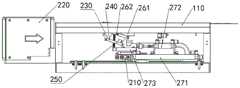
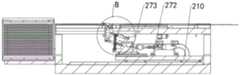
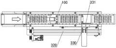
图标:100-滑轨结构;110-导轨;210-运输底座;220-弹夹;230-第一夹持机构;240-连接件;250-压缩弹簧;261-导向凸台;262-止挡块;271-第一左右伸缩模组;272-第二左右伸缩模组;273-滑块;281-上端夹持爪;282-下端夹持爪;283-连接杆;284-磁铁;285-电磁铁;320-左右驱动机构;330-第二夹持机构;331-第一夹爪;3311-第一夹持边沿;332-第二夹爪;3321-第二夹持边沿;333-伸缩缸;334-第一安装座;335-滑动块;336-连接臂;337-第二安装座;338-联动齿轮;400-图像采集检测装置;500-壳体。Icon: 100-slide rail structure; 110-guide rail; 210-transport base; 220-magazine; 230-first clamping mechanism; 240-connector; 250-compression spring; 261-guide boss; 262-stop block; 271-first left and right telescopic modules; 272-second left and right telescopic modules; 273-slider; 281-upper clamping claw; 282-lower clamping claw; 283-connecting rod; 284-magnet; 285- Electromagnet; 320 - left and right drive mechanism; 330 - second clamping mechanism; 331 - first clamping jaw; 3311 - first clamping edge; 332 - second clamping jaw; 3321 - second clamping edge; 333 - telescopic Cylinder; 334-first mounting seat; 335-slide block; 336-connecting arm; 337-second mounting seat; 338-linkage gear; 400-image acquisition and detection device; 500-shell.
具体实施方式Detailed ways
下面将结合实施例对本发明的技术方案进行清楚、完整地描述,显然,所描述的实施例是本发明一部分实施例,而不是全部的实施例。基于本发明中的实施例,本领域普通技术人员在没有做出创造性劳动前提下所获得的所有其他实施例,都属于本发明保护的范围。The technical solutions of the present invention will be clearly and completely described below with reference to the embodiments. Obviously, the described embodiments are part of the embodiments of the present invention, but not all of the embodiments. Based on the embodiments of the present invention, all other embodiments obtained by those of ordinary skill in the art without creative efforts shall fall within the protection scope of the present invention.
如图1-图12所示,本发明实施例提供的所述芯片检测设备包括:滑轨结构100、抽取装置、运输装置和图像采集检测装置400;所述抽取装置用于将弹夹220内的芯片载板抽出并放置在滑轨结构100上;所述运输装置用于将所述滑轨结构100上的芯片载板运输到检测位置,或者将检测位置的芯片载板从检测位置移出;所述图像采集检测装置400位于所述检测位置的上方,用于采集芯片载板上芯片的图像,并将所述图像与标准图像进行比较,从而获取芯片载板上芯片的缺陷。As shown in FIG. 1 to FIG. 12 , the chip detection device provided by the embodiment of the present invention includes: a
如图2所示,可以先将弹夹220与滑轨结构100的首端对齐,然后利用抽取装置从弹夹220中将芯片载板抽出,并放置在滑轨结构100上;然后,利用运输装置向前移动芯片载板,从而使芯片载板运动到图像采集检测装置400下方的检测位置,利用图像采集监测装置采集芯片的图像,将采集到的图像与系统里预存的标准图像进行对比,从而可以得到被检测芯片存在缺陷的位置,检测完的芯片将会被运输装置继续向前运输,从而离开检测位置。然后运输装置再将下一个芯片载板运输到检测位置进行检测。在抽取、运输和检测的过程中,均没有人为的参与,降低了人为污染芯片的风险,利用机械代替人工,可以提高检测的效率和质量。As shown in FIG. 2 , the
芯片检测设备还包括完全覆盖滑轨结构100、抽取装置、运输装置和图像采集检测装置400的壳体500,壳体500上设置有与滑轨结构100的首端和尾端连接的进口和出口,进口设置有托架,托架用于支撑弹夹220。The chip detection device further includes a
所述图像采集检测装置400包括移动平台、图像采集机构和环形光源;所述移动平台能够带动所述图像采集机构沿第一方向和第二方向运动,所述第一方向和第二方向所成的面与滑轨结构100的长度方向垂直;所述环形光源连接在所述图像采集机构的最下端,且所述环形光源的圆心与所述图像采集机构的光轴同轴。The image acquisition and
图像采集机构可以为工业相机,移动平台可以为二维运动平台也可以为三维运动平台,本实施例中,移动平台可以为二维运动,可以带动图像采集机构前后和上下运动,芯片载板上具有多个芯片,通过前后运动图像采集机构,可以使图像采集机构在前后方向上采集到完整的芯片图像;通过上下调整图像采集机构可以方便图像采集机构对焦;因为运输装置可以带动芯片载板沿左右方向运动,可以使图像采集机构在左右方向上采集到芯片载板上完整的芯片图像。并且,在图像采集机构的最下端固定有一个环形的光源,起到补光的作用,从而使拍摄的图像更加清楚。The image acquisition mechanism can be an industrial camera, and the mobile platform can be a two-dimensional motion platform or a three-dimensional motion platform. In this embodiment, the mobile platform can be a two-dimensional motion platform, which can drive the image acquisition mechanism to move back and forth and up and down. There are multiple chips. By moving the image acquisition mechanism back and forth, the image acquisition mechanism can collect a complete chip image in the front and rear directions; by adjusting the image acquisition mechanism up and down, the image acquisition mechanism can be easily focused; because the transport device can drive the chip carrier along the Movement in the left and right directions enables the image acquisition mechanism to acquire a complete chip image on the chip carrier in the left and right directions. In addition, a ring-shaped light source is fixed at the lowermost end of the image acquisition mechanism, which plays the role of supplementary light, thereby making the captured image clearer.
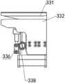
如图3-图8所示,所述抽取装置包括左右输送机构和第一夹持机构230;所述左右输送机构包括运输底座210和线性驱动模组,所述线性驱动模组用于驱动所述运输底座210沿滑轨结构100的长度方向运动;所述第一夹持机构230位于所述运输底座210上,所述第一夹持机构230用于夹住弹夹220内的芯片载板。As shown in FIG. 3-FIG. 8, the extraction device includes a left and right conveying mechanism and a
将滑轨结构100的首端与弹夹220的出口对齐,然后可以利用左右输送机构将运输底座210上的第一夹持机构230运动到弹夹220的出口位置处并同时张开第一夹持机构230,利用第一夹持机构230夹住芯片载板,再利用左右输送机构反向驱动运输底座210,从而可以将芯片载板从弹夹220中拉出来并在滑轨结构100上滑动,然后被输送到检测工位处。Align the head end of the
所述滑轨结构100包括平行且间隔的两道导轨110,所述第一夹持机构230位于所述滑轨结构100的下方;所述第一夹持机构230与所述运输底座210活动连接,所述抽取装置包括第一竖向驱动机构,所述第一竖向驱动机构用于带动所述第一夹持机构230在竖向上运动。The sliding
为了降低抽取装置的宽度,可以将第一夹持机构230设置在滑轨结构100的下方,并且,在第一夹持机构230将芯片载板从弹夹220中取出后,为了不影响后续的芯片载板沿滑轨结构100继续运动,第一夹持机构230可以下降到滑轨结构100的下方,而当需要使用第一夹持机构230时,再利用第一竖向驱动机构提升第一夹持机构230,以使第一夹持机构230的夹嘴与弹夹220的出口平齐。In order to reduce the width of the extraction device, the
所述运输底座210与所述第一夹持机构230通过连接件240连接,所述连接件240的一端与所述运输底座210铰接,所述连接件240的另一端与所述第一夹持机构230铰接;所述第一竖向驱动机构包括压缩弹簧250,所述压缩弹簧250的一端与所述连接件240连接,所述压缩弹簧250的另一端与所述运输底座210连接,所述压缩弹簧250用于使所述第一夹持机构230具有向上运动的趋势;所述连接件240上设置有止挡块262,所述止挡块262与所述导轨110的底面抵接;所述导轨110的底面上设置有导向凸台261,所述导向凸台261朝向所述导轨110首端的面为斜面,自所述导轨110的首端向尾端方向,所述斜面向下倾斜,所述斜面用于引导所述止挡块262向上或者向下运动,以使所述第一夹持机构230上升或者下降。The
本实施例中,运输底座210和第一夹持机构230通过连接件240连接,从而形成平行四边形连接件240机构,连接件240和运输底座210之间压缩有压缩弹簧250,压缩弹簧250可以使连接件240上的止挡块262始终与导轨110的底面抵接。在导轨110远离其首端将近一个芯片载板长度的位置处设置一个导向凸台261,导向凸台261上的斜面朝向导轨110的首端,并向下倾斜,本实施例中,导向凸台261可以呈梯形体。初始时,第一夹持机构230位于导轨110的下方,且止挡块262抵接在导向凸台261的底面上,随着运输底座210朝导轨110的首端运动时,止挡块262沿着斜面向上运动,第一夹持机构230也同时向上运动,从而可以使第一夹持机构230的夹嘴与弹夹220的出口平齐。反之,当第一夹持机构230夹住芯片载板并将芯片载板完全抽出时,第二夹持机构330可以打开夹嘴,止挡块262再次运动到斜面上,并且当运输底座210继续朝远离导轨110首端的方向运动时,止挡块262顺着斜面向下运动,从而可以带动第一夹持机构230向下运动,从而移动到滑轨结构100的下方,被夹出来的芯片载板可以继续沿滑轨结构100运动,并不受到第一夹持机构230的影响。In this embodiment, the
所述线性驱动模组包括第一左右伸缩模组271和第二左右伸缩模组272;所述运输底座210上滑动连接有滑块273,所述滑块273的滑动方向与所述滑轨结构100的长度方向相同,所述第一夹持机构230和第二左右伸缩模组272固定在所述滑块273上;所述第一左右伸缩模组271与所述运输底座210连接,用于驱动所述运输底座210、滑块273和第一夹持机构230沿横向运动,所述第二左右伸缩模组272与所述滑块273连接,用于驱动所述滑块273和第一夹持机构230沿横向运动。The linear drive module includes a first left and right
为了使第一夹持机构230可以顺畅的夹取及释放芯片载板,本实施例中,初始时,可以先利用第一左右伸缩模组271推动运输底座210,将运输底座210上的滑块273、第一夹持机构230和第二左右伸缩模组272均向导轨110的首端推动,通过设置第一左右伸缩模组271的伸长长度,可以使第一夹持机构230停在靠近弹夹220出口的位置处,然后控制第一夹持机构230张开夹嘴,然后再利用第一左右伸缩模组271继续朝导轨110的前端推动滑块273,以使第一夹持机构230的夹嘴正好运动到芯片载板的边缘处,第一夹持机构230闭合夹嘴将芯片载板的边缘夹持。然后第一左右伸缩模组271反向拉动运输底座210,将芯片载板完全抽出,此时,止挡块262位于导向凸台261斜面的前端,然后,第一夹持机构230张开夹嘴,第二左右伸缩模组272继续带动滑块273向后运动,第一夹持机构230因为止挡块262与导向凸台261的相互作用而向下运动。In order to enable the
所述第一夹持机构230包括上端夹持爪281、下端夹持爪282和第一竖向驱动机构,所述第一竖向驱动机构的活动端与所述上端夹持爪281连接,用于带动所述上端夹持爪281朝向或者远离下端夹持爪282运动;所述第一竖向驱动机构包括连接杆283、磁铁284、电磁铁285,所述磁铁284和电磁铁285固定在所述下端夹持爪282上,所述磁铁284能够沿所述上端夹持爪281和下端夹持爪282的开合方向,朝向或者远离所述电磁铁285运动;所述连接杆283的一端与所述磁铁284连接,另一端与所述上端夹持爪281铰接。The
可以通过改变电磁铁285的极性,从而排斥磁铁284或者吸引磁铁284,当电磁铁285与磁铁284相互排斥时,磁铁284通过连接杆283向上推动上端夹持爪281,从而使上端夹持爪281和下端夹持爪282的展开;而当电磁铁285与磁铁284相互吸引时,连接杆283向下拉动上端夹持爪281,从而使上端夹持爪281和下端夹持爪282闭合夹持芯片载板。The polarity of the
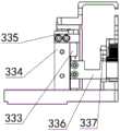
所述滑轨结构100包括平行且间隔的两道导轨110,所述运输装置还包括第二夹持机构330和左右驱动机构320,所述左右驱动机构320用于带动所述第二夹持机构330沿与所述导轨110平行的方向运动;至少一个所述导轨110的侧面设置有第二夹持机构330,所述第二夹持机构330包括能够开合的第一夹爪331和第二夹爪332,以及第二竖向驱动机构;所述第二夹爪332包括位于两道导轨110之间的第二夹持边沿3321;所述第一夹爪331包括滑槽,所述滑槽的扣在所述导轨110上,且所述滑槽包括间隔设置的两个槽壁,位于两道所述导轨110之间的槽壁与所述第二夹持边沿3321对齐以形成第一夹持边沿3311;所述第二竖向驱动机构用于驱动所述第一夹爪331和第二夹爪332开合。The
左右驱动机构320可以为丝杆电机模组,以电机为动力源驱动丝杆转动,以使丝杆上的滑块沿丝杆长度方向运动,第二夹持机构330固定在滑块273上。The left and
所述第二夹爪332包括位于两道导轨110之间的第二夹持边沿3321;所述第一夹爪331包括滑槽,所述滑槽的扣在所述导轨110上,并半包裹导轨110。所述滑槽包括间隔设置的两个槽壁,位于两道所述导轨110之间的槽壁与所述第二夹持边沿3321对齐以形成第一夹持边沿3311。芯片载板被抽出后放置在导轨110上,导轨110上的第二夹持机构330可以夹住芯片载板,然后左右驱动机构320可以带动芯片载板沿导轨110的长度方向运动,可以运动到检测位置,或者带动检测后的芯片载板到达出料位置,在传送的过程中,芯片载板不再人为手动传送,避免了对芯片造成人为的污染,提高了检测质量和检测效率。并且,第二夹持机构330的第一夹持边沿3311和第二夹持边沿3321形成的结构包裹在导轨110的外侧,降低了第二夹持机构330占用的空间,通过合理的结构设计,使产品结构紧凑,且空间占用小。The
所述第二竖向驱动机构包括伸缩缸333、第一安装座334、滑动块335,连接臂336、第二安装座337、联动齿轮338;沿所述第一夹爪331和第二夹爪332的开合方向,所述滑动块335与所述第一安装座334滑动连接,所述第一夹爪331与所述滑动块335连接,所述连接臂336的一端与所述滑动块335连接,所述连接臂336的另一端设置有第一齿条部,所述第一齿条部与所述联动齿轮338啮合;所述联动齿轮338转动连接在所述第二安装座337上,所述第二夹爪332的侧壁上设置有第二齿条部,所述第二齿条部与所述联动齿轮338啮合,且所述第一齿条部和第二齿条部分别位于所述联动齿轮338的相对两侧;沿所述第一夹爪331和第二夹爪332的开合方向,所述第二夹爪332与所述第二安装座337滑动连接;所述伸缩缸333固定在所述第一安装座334上,所述伸缩缸333的活动端与所述连接臂336连接,用于带动所述连接臂336沿所述第一夹爪331和第二夹爪332的开合方向运动。The second vertical drive mechanism includes a telescopic cylinder 333, a first mounting seat 334, a sliding block 335, a connecting arm 336, a second mounting seat 337, and a linkage gear 338; along the first clamping jaw 331 and the second clamping jaw 332, the sliding block 335 is slidably connected with the first mounting seat 334, the first clamping jaw 331 is connected with the sliding block 335, and one end of the connecting arm 336 is connected with the sliding block 335 The other end of the connecting arm 336 is provided with a first rack portion, and the first rack portion is engaged with the linkage gear 338; the linkage gear 338 is rotatably connected to the second mounting seat 337, A second rack portion is provided on the side wall of the second clamping jaw 332, the second rack portion is engaged with the linkage gear 338, and the first rack portion and the second rack portion are respectively located at the The opposite sides of the linkage gear 338; along the opening and closing directions of the first jaw 331 and the second jaw 332, the second jaw 332 is slidably connected to the second mounting seat 337; the telescopic The cylinder 333 is fixed on the first mounting seat 334, and the movable end of the telescopic cylinder 333 is connected with the connecting arm 336 for driving the connecting arm 336 along the first clamping jaw 331 and the second clamping jaw 332 moves in the opening and closing directions.
本实施例中,所述第二竖向驱动机构分别与所述第一夹爪331和第二夹爪332连接,用于驱动所述第一夹爪331和第二夹爪332相对运动。通过设置第一夹爪331和第二夹爪332相对/反向运动从而实现第二夹持机构330的开合,可以适应不同厚度的芯片载板,避免第一夹爪331和第二夹爪332其中的一者不动对载板芯片产生止挡问题。伸缩缸333带动连接臂336上下运动,当连接臂336向下运动时,与连接臂336直接连接的滑块273将带动第一夹爪331向下运动;同时,连接臂336带动联动齿轮338朝正向旋转,联动齿轮338带动第二夹爪332向下运动,从而使第二夹持机构330展开;反之,当伸缩缸333驱动连接臂336向下运动时,第二夹持机构330闭合将芯片载板夹持。In this embodiment, the second vertical driving mechanism is respectively connected with the
所述滑轨结构100上还具有初始位置和出料位置,所述初始位置的末端设置有第一接近开关,所述检测位置的末端设置第二接近开关,所述出料位置的位置设置有第三接近开关,所述第一接近开关、第二接近开关和第三接近开关均与所述左右驱动机构320电连接。The
当芯片载板位于初始位置时,第一接近开关被触发,假设此时第二接近开关没有被触发,那么左右驱动机构320可以带动第二夹持机构330运动到初始位置,将初始位置的芯片载板运输到检测位置,通过第一接近开关、第二接近开关和第三接近开关可以检测各个位置上是否存在芯片载板,如果某一位置上的接近开关没有检测到芯片载板,那么第二夹持机构330就可以将前一个位置上的芯片载板移动到下一个位置,从而使传送一直继续。When the chip carrier is at the initial position, the first proximity switch is triggered. Assuming that the second proximity switch is not triggered at this time, the left and
最后应说明的是:以上各实施例仅用以说明本发明的技术方案,而非对其限制;尽管参照前述各实施例对本发明进行了详细的说明,本领域的普通技术人员应当理解:其依然可以对前述各实施例所记载的技术方案进行修改,或者对其中部分或者全部技术特征进行等同替换;而这些修改或者替换,并不使相应技术方案的本质脱离本发明各实施例技术方案的范围。Finally, it should be noted that the above embodiments are only used to illustrate the technical solutions of the present invention, but not to limit them; although the present invention has been described in detail with reference to the foregoing embodiments, those of ordinary skill in the art should understand that: The technical solutions described in the foregoing embodiments can still be modified, or some or all of the technical features thereof can be equivalently replaced; and these modifications or replacements do not make the essence of the corresponding technical solutions deviate from the technical solutions of the embodiments of the present invention. scope.
Claims (10)
Priority Applications (1)
| Application Number | Priority Date | Filing Date | Title |
|---|---|---|---|
| CN202010956644.3ACN111948220B (en) | 2020-09-11 | 2020-09-11 | Chip detection equipment |
Applications Claiming Priority (1)
| Application Number | Priority Date | Filing Date | Title |
|---|---|---|---|
| CN202010956644.3ACN111948220B (en) | 2020-09-11 | 2020-09-11 | Chip detection equipment |
Publications (2)
| Publication Number | Publication Date |
|---|---|
| CN111948220Atrue CN111948220A (en) | 2020-11-17 |
| CN111948220B CN111948220B (en) | 2025-08-19 |
Family
ID=73356857
Family Applications (1)
| Application Number | Title | Priority Date | Filing Date |
|---|---|---|---|
| CN202010956644.3AActiveCN111948220B (en) | 2020-09-11 | 2020-09-11 | Chip detection equipment |
Country Status (1)
| Country | Link |
|---|---|
| CN (1) | CN111948220B (en) |
Cited By (2)
| Publication number | Priority date | Publication date | Assignee | Title |
|---|---|---|---|---|
| CN112834527A (en)* | 2020-12-31 | 2021-05-25 | 江苏理工学院 | QFN chip image acquisition device and image acquisition method thereof |
| CN116242780A (en)* | 2023-05-11 | 2023-06-09 | 山东工业职业学院 | Computer chip detection equipment and method based on image recognition |
Citations (14)
| Publication number | Priority date | Publication date | Assignee | Title |
|---|---|---|---|---|
| DE2454825A1 (en)* | 1974-11-19 | 1976-05-26 | Norbert Weiner | Handling device for small components - places them on circuit boards on removes them from circuit boards using spring loaded gripping claw |
| CN101493425A (en)* | 2008-10-31 | 2009-07-29 | 东莞康视达自动化科技有限公司 | Full automatic ultraviolet optical detection method for microscopic surface flaw and system thereof |
| CN104568965A (en)* | 2014-12-20 | 2015-04-29 | 佛山市多谱光电科技有限公司 | Method and device for detecting defects of LED light source chip |
| US20160060046A1 (en)* | 2014-08-29 | 2016-03-03 | Sysmex Corporation | Transport apparatus and transport method |
| CN107402219A (en)* | 2017-08-21 | 2017-11-28 | 苏州巨智能装备有限公司 | Battery core apparent visual detection device and its detection method |
| CN208736809U (en)* | 2018-08-06 | 2019-04-12 | 深圳明锐理想科技有限公司 | A kind of integral type chip bonding automated optical detection equipment |
| CN109712918A (en)* | 2018-12-29 | 2019-05-03 | 铜陵富仕三佳机器有限公司 | Chip detects collecting device and its application method |
| CN109911602A (en)* | 2019-03-27 | 2019-06-21 | 夏安祥 | A kind of chip automatic charging device for welding circuit board |
| CN110227655A (en)* | 2019-04-29 | 2019-09-13 | 丽水奇异果信息技术有限公司 | A kind of chip-detecting apparatus based on image recognition |
| CN110596138A (en)* | 2019-08-14 | 2019-12-20 | 深圳格兰达智能装备股份有限公司 | IC material strip visual detection and ink dot marking equipment |
| CN110817241A (en)* | 2019-11-18 | 2020-02-21 | 湖北中纬幸和自动化设备科技有限公司 | Detection apparatus for PCB board |
| CN110828348A (en)* | 2019-11-19 | 2020-02-21 | 南京泰治自动化技术有限公司 | A substrate assembling device and assembling control system and method |
| CN111060529A (en)* | 2019-11-11 | 2020-04-24 | 深圳市世椿智能装备股份有限公司 | Defect detection equipment and method for hydrogen fuel cell chip |
| CN212341037U (en)* | 2020-09-11 | 2021-01-12 | 浙江水晶光电科技股份有限公司 | Chip detection equipment |
- 2020
- 2020-09-11CNCN202010956644.3Apatent/CN111948220B/enactiveActive
Patent Citations (14)
| Publication number | Priority date | Publication date | Assignee | Title |
|---|---|---|---|---|
| DE2454825A1 (en)* | 1974-11-19 | 1976-05-26 | Norbert Weiner | Handling device for small components - places them on circuit boards on removes them from circuit boards using spring loaded gripping claw |
| CN101493425A (en)* | 2008-10-31 | 2009-07-29 | 东莞康视达自动化科技有限公司 | Full automatic ultraviolet optical detection method for microscopic surface flaw and system thereof |
| US20160060046A1 (en)* | 2014-08-29 | 2016-03-03 | Sysmex Corporation | Transport apparatus and transport method |
| CN104568965A (en)* | 2014-12-20 | 2015-04-29 | 佛山市多谱光电科技有限公司 | Method and device for detecting defects of LED light source chip |
| CN107402219A (en)* | 2017-08-21 | 2017-11-28 | 苏州巨智能装备有限公司 | Battery core apparent visual detection device and its detection method |
| CN208736809U (en)* | 2018-08-06 | 2019-04-12 | 深圳明锐理想科技有限公司 | A kind of integral type chip bonding automated optical detection equipment |
| CN109712918A (en)* | 2018-12-29 | 2019-05-03 | 铜陵富仕三佳机器有限公司 | Chip detects collecting device and its application method |
| CN109911602A (en)* | 2019-03-27 | 2019-06-21 | 夏安祥 | A kind of chip automatic charging device for welding circuit board |
| CN110227655A (en)* | 2019-04-29 | 2019-09-13 | 丽水奇异果信息技术有限公司 | A kind of chip-detecting apparatus based on image recognition |
| CN110596138A (en)* | 2019-08-14 | 2019-12-20 | 深圳格兰达智能装备股份有限公司 | IC material strip visual detection and ink dot marking equipment |
| CN111060529A (en)* | 2019-11-11 | 2020-04-24 | 深圳市世椿智能装备股份有限公司 | Defect detection equipment and method for hydrogen fuel cell chip |
| CN110817241A (en)* | 2019-11-18 | 2020-02-21 | 湖北中纬幸和自动化设备科技有限公司 | Detection apparatus for PCB board |
| CN110828348A (en)* | 2019-11-19 | 2020-02-21 | 南京泰治自动化技术有限公司 | A substrate assembling device and assembling control system and method |
| CN212341037U (en)* | 2020-09-11 | 2021-01-12 | 浙江水晶光电科技股份有限公司 | Chip detection equipment |
Cited By (2)
| Publication number | Priority date | Publication date | Assignee | Title |
|---|---|---|---|---|
| CN112834527A (en)* | 2020-12-31 | 2021-05-25 | 江苏理工学院 | QFN chip image acquisition device and image acquisition method thereof |
| CN116242780A (en)* | 2023-05-11 | 2023-06-09 | 山东工业职业学院 | Computer chip detection equipment and method based on image recognition |
Also Published As
| Publication number | Publication date |
|---|---|
| CN111948220B (en) | 2025-08-19 |
Similar Documents
| Publication | Publication Date | Title |
|---|---|---|
| CN107051900B (en) | A kind of automation equipment applied to bearing on-line detection | |
| CN109499918B (en) | Pipe joint visual inspection device | |
| CN110948227A (en) | Mainboard assembly line | |
| CN111948220A (en) | Chip testing equipment | |
| CN109759342B (en) | A device suitable for defect detection of flat motors of mobile phones and its implementation method | |
| CN110479641A (en) | A kind of quality inspection automation equipment for aircraft bearing | |
| CN112893154B (en) | Screw straightness accuracy detection mechanism and screw automation detection equipment | |
| CN114377998A (en) | Zipper detection and removal device and detection and sorting method | |
| CN114813777A (en) | Automatic chip detection device | |
| CN217586975U (en) | Automatic chip detection device | |
| CN111322933A (en) | Automatic change plane degree detection device | |
| CN209021587U (en) | Automatic assembling machine for contact pieces in safety lock pieces of front-loading washing machines | |
| CN111721778A (en) | Vertical visual inspection equipment for chip defects | |
| CN209565257U (en) | Automatic online visual inspection device for appearance defects of motor commutator | |
| CN212341037U (en) | Chip detection equipment | |
| CN112171265A (en) | Sliding switch sliding cover assembly equipment and sliding switch assembly system | |
| CN108683053A (en) | A kind of USB connector full-automatic assembly equipment and technique | |
| CN101169452B (en) | Ceramic tile quality detection method and apparatus | |
| CN207030360U (en) | A kind of feed device of optical detection apparatus | |
| CN116637829A (en) | A fully automatic filter thread detection machine | |
| CN109211172A (en) | A kind of roundness measurement device testing agency | |
| CN115569869A (en) | Automatic detection and sorting equipment for optical device bonding wires | |
| CN210037654U (en) | Egg shell dark spot detection and sorting device | |
| CN219378069U (en) | Battery rear cover appearance detection equipment | |
| CN115709179B (en) | Automated optical inspection equipment for QFN chips |
Legal Events
| Date | Code | Title | Description |
|---|---|---|---|
| PB01 | Publication | ||
| PB01 | Publication | ||
| SE01 | Entry into force of request for substantive examination | ||
| SE01 | Entry into force of request for substantive examination | ||
| GR01 | Patent grant | ||
| GR01 | Patent grant |