CN111945202A - Blind Via Plating Method for Ceramic Leadless Housings - Google Patents
Blind Via Plating Method for Ceramic Leadless HousingsDownload PDFInfo
- Publication number
- CN111945202A CN111945202ACN202010706302.6ACN202010706302ACN111945202ACN 111945202 ACN111945202 ACN 111945202ACN 202010706302 ACN202010706302 ACN 202010706302ACN 111945202 ACN111945202 ACN 111945202A
- Authority
- CN
- China
- Prior art keywords
- electroplating
- hole
- ceramic
- green ceramic
- plating
- Prior art date
- Legal status (The legal status is an assumption and is not a legal conclusion. Google has not performed a legal analysis and makes no representation as to the accuracy of the status listed.)
- Granted
Links
Images


Classifications
- C—CHEMISTRY; METALLURGY
- C25—ELECTROLYTIC OR ELECTROPHORETIC PROCESSES; APPARATUS THEREFOR
- C25D—PROCESSES FOR THE ELECTROLYTIC OR ELECTROPHORETIC PRODUCTION OF COATINGS; ELECTROFORMING; APPARATUS THEREFOR
- C25D5/00—Electroplating characterised by the process; Pretreatment or after-treatment of workpieces
- C25D5/54—Electroplating of non-metallic surfaces
- C—CHEMISTRY; METALLURGY
- C25—ELECTROLYTIC OR ELECTROPHORETIC PROCESSES; APPARATUS THEREFOR
- C25D—PROCESSES FOR THE ELECTROLYTIC OR ELECTROPHORETIC PRODUCTION OF COATINGS; ELECTROFORMING; APPARATUS THEREFOR
- C25D5/00—Electroplating characterised by the process; Pretreatment or after-treatment of workpieces
- C25D5/02—Electroplating of selected surface areas
Landscapes
- Chemical & Material Sciences (AREA)
- Engineering & Computer Science (AREA)
- Chemical Kinetics & Catalysis (AREA)
- Electrochemistry (AREA)
- Materials Engineering (AREA)
- Metallurgy (AREA)
- Organic Chemistry (AREA)
- Ceramic Capacitors (AREA)
Abstract
Translated fromChinese
Description
Translated fromChinese技术领域technical field
本发明属于电子封装技术领域,更具体地说,是涉及一种陶瓷无引线外壳的盲孔电镀方法。The invention belongs to the technical field of electronic packaging, and more particularly relates to a blind hole electroplating method for a ceramic leadless casing.
背景技术Background technique
陶瓷无引线外壳典型结构如图8至10所示。大多数这类外壳侧壁均设有与引出焊盘相连的空心金属化孔,该空心金属化孔的作用是起互连作用或加强与印制电路板的焊接可靠性,这类孔多数为盲孔结构,产品制备过程需通过电镀工艺实现镀覆。Typical structures of ceramic leadless enclosures are shown in Figures 8 to 10. Most of these shell side walls are provided with hollow metallized holes connected to the lead-out pads. The function of the hollow metallized holes is to interconnect or enhance the reliability of soldering with the printed circuit board. Most of these holes are Blind hole structure, the product preparation process needs to be plated through an electroplating process.
但由于该类外壳无外引线,且尺寸较小,采用传统的单个外壳绑丝电镀工艺,成品率和效率极低。However, since this type of casing has no outer leads and is small in size, the traditional single-shell wire-binding electroplating process is used, and the yield and efficiency are extremely low.
发明内容SUMMARY OF THE INVENTION
本发明的目的在于提供一种陶瓷无引线外壳的盲孔电镀方法,旨在解决现有陶瓷无引线外壳电镀盲孔时,成品率和效率低的问题。The purpose of the present invention is to provide a blind hole electroplating method for a ceramic leadless casing, which aims to solve the problems of low yield and efficiency when electroplating blind holes in the existing ceramic leadless casing.
为实现上述目的,本发明采用的技术方案是:提供一种陶瓷无引线外壳的盲孔电镀方法,包括:In order to achieve the above purpose, the technical solution adopted in the present invention is to provide a blind hole electroplating method for a ceramic leadless casing, comprising:
生瓷冲孔:Green Porcelain Punching:
获取下结构层的生瓷片的制作区域,在该制作区域外冲制第一电镀孔,所述第一电镀孔的内端形成待制备的陶瓷无引线外壳的侧面盲孔;Obtaining the production area of the green ceramic sheet of the lower structural layer, punching a first electroplating hole outside the production area, the inner end of the first electroplating hole forms the side blind hole of the ceramic leadless casing to be prepared;
获取上结构层的生瓷片的制作区域,在该制作区域外冲制第二电镀孔;Obtain the production area of the green ceramic sheet of the upper structural layer, and punch a second electroplating hole outside the production area;
所述上结构层的生瓷片的四周侧面以及所述下结构层的生瓷片四周侧面冲制上下贯通的电镀绑丝孔;The surrounding sides of the green ceramic sheets of the upper structural layer and the surrounding sides of the green ceramic sheets of the lower structural layer are punched with electroplating wire-binding holes that penetrate up and down;
所述上结构层和所述下结构层层压后,同一制作区域外的所述第二电镀孔和所述第一电镀孔上下连通;After the upper structure layer and the lower structure layer are laminated, the second electroplating hole and the first electroplating hole outside the same production area are connected up and down;
印制金属化图形:在生瓷片埋层印刷电镀线,使各所述制作区域之间以及与所述电镀绑丝孔之间实现电互联;Printing metallization patterns: printing electroplating lines on the buried layers of green ceramic sheets to achieve electrical interconnection between the fabrication areas and the electroplating wire-binding holes;
孔金属化:对所述第一电镀孔、所述第二电镀孔、所述侧面盲孔以及所述电镀绑丝孔金属化;Hole metallization: metallize the first electroplated hole, the second electroplated hole, the side blind hole and the electroplated wire-binding hole;
层压:对上结构层的生瓷片和下结构层的生瓷片压制成型;Lamination: pressing and molding the green ceramic sheets of the upper structural layer and the green ceramic sheets of the lower structural layer;
电镀:利用金属丝穿过相对两侧的所述电镀绑丝孔绑扎电镀,电镀时,电镀液从所述第一电镀孔和所述第二电镀孔流过,实现侧面盲孔的镀覆;Electroplating: use metal wires to pass through the electroplating wire binding holes on opposite sides to bind electroplating. During electroplating, the electroplating solution flows through the first electroplating hole and the second electroplating hole to realize the plating of side blind holes;
切割分离:沿层压后的所述制作区域的四边切割,制成单个陶瓷无引线外壳。Cutting and separation: cutting along the four sides of the laminated production area to make a single ceramic leadless housing.
作为本申请另一实施例,所述第一电镀孔为长条孔,所述长条孔的两端均为半圆形,所述长条孔的长度方向与所述制作区域对应的边垂直。As another embodiment of the present application, the first electroplating hole is an elongated hole, both ends of the elongated hole are semicircular, and the length direction of the elongated hole is perpendicular to the side corresponding to the production area .
作为本申请另一实施例,所述第二电镀孔为圆孔,所述圆孔的中心与所述长条孔远离所述制作区域的一端的半圆形孔同轴。As another embodiment of the present application, the second plated hole is a circular hole, and the center of the circular hole is coaxial with the semicircular hole at the end of the elongated hole away from the production area.
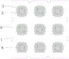
作为本申请另一实施例,所述生瓷片上设有若干阵列排布的制作区域,每个所述制作区域四周均设有所述第一电镀孔或所述第二电镀孔。As another embodiment of the present application, the green ceramic sheet is provided with a plurality of fabrication areas arranged in an array, and the first electroplating hole or the second electroplating hole is disposed around each of the fabrication areas.
作为本申请另一实施例,所述生瓷片的四周侧面对称设有所述电镀绑丝孔,所述生瓷片的每个侧面分别设有至少两个所述电镀绑丝孔。As another embodiment of the present application, the electroplating wire binding holes are symmetrically provided on the surrounding sides of the green ceramic sheet, and each side surface of the green ceramic sheet is respectively provided with at least two electroplating wire binding holes.
作为本申请另一实施例,所述电镀绑丝孔为弧形孔。As another embodiment of the present application, the electroplating wire binding hole is an arc-shaped hole.
作为本申请另一实施例,所述层压过程中,将生瓷片压制成型后,切割成多个包括多个制作区域的生瓷件,再烧结成熟瓷件,每个所述生瓷件的四周侧面均设有所述电镀绑丝孔。As another embodiment of the present application, in the lamination process, after the green ceramic sheet is pressed into shape, it is cut into a plurality of green ceramic pieces including a plurality of production areas, and then the mature ceramic pieces are sintered. The electroplating wire binding holes are provided on the surrounding sides of the device.
作为本申请另一实施例,所述生瓷件的外形为正方形,或者为长方形。As another embodiment of the present application, the shape of the green ceramic piece is a square or a rectangle.
作为本申请另一实施例,所述电镀液为镍镀液或金镀液。As another embodiment of the present application, the electroplating solution is a nickel plating solution or a gold plating solution.
本发明提供的陶瓷无引线外壳的盲孔电镀方法的有益效果在于:与现有技术相比,本发明陶瓷无引线外壳的盲孔电镀方法,在陶瓷无引线外壳的制作区域外对应的设置上下连通的电镀孔,而陶瓷无引线外壳的侧面盲孔即为第一电镀孔的内侧壁,对阵列分布的若干陶瓷无引线外壳进行电镀,电镀时,电镀液经第一电镀孔和第二电镀孔流通,对侧面盲孔的侧壁和孔底实现电镀,由于电镀液在侧面盲孔内流动,提高了对侧壁盲孔镀层的均匀性,提高了电镀的质量,进而提高了成品率;同时能够电镀多个陶瓷无引线外壳,大大提高了电镀效率,提高了成品的制作效率。The beneficial effect of the blind hole electroplating method for the ceramic leadless casing provided by the present invention is that, compared with the prior art, the blind hole electroplating method for the ceramic leadless casing of the present invention is arranged correspondingly up and down outside the production area of the ceramic leadless casing. The connected electroplating holes, and the side blind holes of the ceramic leadless casing are the inner side walls of the first electroplating hole, and several ceramic leadless casings distributed in an array are electroplated. During electroplating, the electroplating solution passes through the first electroplating hole and the second electroplating hole. Through hole circulation, electroplating is realized on the side wall and hole bottom of the side blind hole. Since the electroplating solution flows in the side blind hole, the uniformity of the plating layer on the side wall blind hole is improved, the quality of electroplating is improved, and the yield is improved; At the same time, a plurality of ceramic leadless shells can be electroplated, which greatly improves the electroplating efficiency and improves the production efficiency of the finished product.
附图说明Description of drawings
为了更清楚地说明本发明实施例中的技术方案,下面将对实施例或现有技术描述中所需要使用的附图作简单地介绍,显而易见地,下面描述中的附图仅仅是本发明的一些实施例,对于本领域普通技术人员来讲,在不付出创造性劳动的前提下,还可以根据这些附图获得其他的附图。In order to illustrate the technical solutions in the embodiments of the present invention more clearly, the following briefly introduces the accompanying drawings that need to be used in the description of the embodiments or the prior art. Obviously, the drawings in the following description are only for the present invention. In some embodiments, for those of ordinary skill in the art, other drawings can also be obtained according to these drawings without any creative effort.
图1为本发明实施例提供的陶瓷无引线外壳的盲孔电镀方法中生瓷冲孔后下结构层的结构示意图;1 is a schematic structural diagram of a lower structural layer after green ceramic punching in a blind hole electroplating method for a ceramic leadless casing provided by an embodiment of the present invention;
图2为本发明实施例提供的陶瓷无引线外壳的盲孔电镀方法中生瓷冲孔后上结构层的结构示意图;2 is a schematic structural diagram of an upper structural layer after green ceramic punching in a blind hole electroplating method for a ceramic leadless casing provided by an embodiment of the present invention;
图3为本发明实施例提供的陶瓷无引线外壳的盲孔电镀方法中印制金属化图形后下结构层的结构示意图;3 is a schematic structural diagram of a lower structural layer after a metallization pattern is printed in a blind hole electroplating method for a ceramic leadless casing provided by an embodiment of the present invention;
图4为本发明实施例提供的陶瓷无引线外壳的盲孔电镀方法中印制金属化图形后上结构层的结构示意图;4 is a schematic structural diagram of an upper structural layer after a metallization pattern is printed in a blind hole electroplating method for a ceramic leadless casing provided by an embodiment of the present invention;
图5为本发明实施例提供的陶瓷无引线外壳的盲孔电镀方法中层压后一个制作区域的背面结构示意图;5 is a schematic diagram of a backside structure of a fabrication area after lamination in the blind hole electroplating method for a ceramic leadless casing provided by an embodiment of the present invention;
图6为本发明实施例提供的陶瓷无引线外壳的盲孔电镀方法中层压后一个制作区域的正面结构示意图;6 is a schematic diagram of the front structure of a manufacturing area after lamination in the blind hole electroplating method of the ceramic leadless casing provided by the embodiment of the present invention;
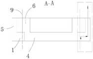
图7为沿图6中A-A线剖切后的切面结构示意图图;7 is a schematic view of the cross-sectional structure after cutting along the line A-A in FIG. 6;
图8为本发明实施例提供的陶瓷无引线外壳的主视结构图;8 is a front structural view of a ceramic leadless housing provided by an embodiment of the present invention;
图9为图8提供的陶瓷无引线外壳的背面结构示意图;FIG. 9 is a schematic view of the back structure of the ceramic leadless housing provided in FIG. 8;
图10为图8提供的陶瓷无引线外壳的正面结构示意图。FIG. 10 is a schematic view of the front structure of the ceramic leadless housing provided in FIG. 8 .
图中:1、电镀绑丝孔;2、第一电镀孔;3、制作区域;4、下结构层;5、第二电镀孔;6、上结构层;7、引出焊盘;8、芯片安装区;9、外形轮廓线;10、盲孔;In the figure: 1. Electroplating wire binding hole; 2. First electroplating hole; 3. Manufacturing area; 4. Lower structure layer; 5. Second electroplating hole; 6. Upper structure layer; 7. Lead-out pad; Installation area; 9. Outline outline; 10. Blind hole;
具体实施方式Detailed ways
为了使本发明所要解决的技术问题、技术方案及有益效果更加清楚明白,以下结合附图及实施例,对本发明进行进一步详细说明。应当理解,此处所描述的具体实施例仅仅用以解释本发明,并不用于限定本发明。In order to make the technical problems, technical solutions and beneficial effects to be solved by the present invention clearer, the present invention will be further described in detail below with reference to the accompanying drawings and embodiments. It should be understood that the specific embodiments described herein are only used to explain the present invention, but not to limit the present invention.
请一并参阅图1至图10,现对本发明提供的陶瓷无引线外壳的盲孔电镀方法进行说明。所述陶瓷无引线外壳的盲孔电镀方法,包括如下步骤:生瓷冲孔、印制金属化图形、孔金属化、层压、电镀和切割分离;Please refer to FIG. 1 to FIG. 10 together, and now the blind hole electroplating method of the ceramic leadless casing provided by the present invention will be described. The blind hole electroplating method of the ceramic leadless housing includes the following steps: punching green ceramics, printing metallized patterns, hole metallization, lamination, electroplating, and cutting and separation;
参见图1及图2,所述生瓷冲孔过程如下:获取下结构层4的生瓷片的制作区域3,在该制作区域3外冲制第一电镀孔2,所述第一电镀孔2的内端形成待制备的陶瓷无引线外壳的侧面盲孔10;侧面盲孔10也即空心金属化孔;Referring to FIGS. 1 and 2 , the green ceramic punching process is as follows: a
获取上结构层6的生瓷片的制作区域3,在该制作区域3外冲制第二电镀孔5;Obtain the
所述上结构层6的生瓷片的四周侧面以及所述下结构层4的生瓷片四周侧面冲制上下贯通的电镀绑丝孔1;The surrounding sides of the green ceramic sheets of the upper
所述上结构层6和所述下结构层4层压后,同一制作区域3外的所述第二电镀孔5和所述第一电镀孔2上下连通;After the
所述印制金属化图形过程如下:在生瓷片埋层印刷电镀线,使各所述制作区域3之间以及与所述电镀绑丝孔1之间实现电互联;The process of printing the metallization pattern is as follows: printing electroplating lines on the buried layer of the green ceramic sheet, so as to realize electrical interconnection between the
所述孔金属化过程如下:对所述第一电镀孔2、所述第二电镀孔5、所述侧面盲孔10以及所述电镀绑丝孔1金属化;The hole metallization process is as follows: metallizing the
参见图3及图4,层压时,对上结构层6的生瓷片和下结构层4的生瓷片压制成型;3 and 4, during lamination, the green ceramic sheets of the upper
电镀时,利用金属丝过所述电镀绑丝孔1进行绑扎电镀,电镀时,电镀液从所述第一电镀孔2和所述第二电镀孔5流过,实现侧面盲孔10的镀覆;参见图5至图7;During electroplating, metal wires are used to pass through the electroplating
切割分离时,沿层压后的所述制作区域3的四边切割,制成单个陶瓷无引线外壳,参见图8至图10。其中,陶瓷无引线外壳的背面设有引出焊盘7,正面腔体内设有芯片安装区8。When cutting and separating, cut along the four sides of the
本发明提供的陶瓷无引线外壳的盲孔电镀方法,与现有技术相比,在陶瓷无引线外壳的制作区域3外对应的设置上下连通的电镀孔,而陶瓷无引线外壳的侧面盲孔10即为第一电镀孔2的内侧壁,电镀时,电镀液经第一电镀孔2和第二电镀孔5流通,对侧面盲孔10的侧壁和孔底实现电镀,由于电镀液在侧面盲孔内流动,提高了对侧壁盲孔10镀层的均匀性,提高了电镀的质量,进而提高了成品率;同时能够电镀多个陶瓷无引线外壳,大大提高了电镀效率,提高了成品的制作效率。Compared with the prior art, in the blind hole electroplating method of the ceramic leadless casing provided by the present invention, electroplating holes connected up and down are correspondingly arranged outside the
其中,在生瓷片上阵列设有若干制作区域3,每个制作区域3对应制作一个陶瓷无引线外壳。其中,下结构层4和上结构层6均包括若干陶瓷片,下结构层4对应成品陶瓷无引线外壳的背面,上结构层6对应成品的陶瓷无引线外壳的正面。陶瓷片为采用流延工艺制成。Among them, a plurality of
在切割分离过程中,沿图6所示的外轮廓线9切割,将第一电镀孔2和第二电镀孔5部位切除。During the cutting and separation process, the first plated
在印制金属化图形中,需要将电互联到电镀绑丝孔1,以便于电镀。In the printed metallization pattern, it is necessary to connect the electrical interconnection to the electroplating
本发明实施例提供的电镀方法,仅仅包括了与本发明点相关的步骤,制备陶瓷无引线外壳,完整的制作方法包括:流延、制网、落料冲孔、金属化印制、空心金属化、层压成型、烧结、镀镍、镀金、分离。The electroplating method provided by the embodiment of the present invention only includes the steps related to the present invention to prepare the ceramic leadless casing. The complete manufacturing method includes: casting, mesh making, blanking and punching, metallized printing, hollow metal chemical, lamination, sintering, nickel plating, gold plating, separation.
其中,空心金属化采用金属钨,电镀镍金是形成保护层。Among them, metal tungsten is used for hollow metallization, and nickel-gold electroplating is used to form a protective layer.
作为本发明提供的陶瓷无引线外壳的盲孔电镀方法的一种具体实施方式,请参阅图1至图4,所述第一电镀孔2为长条孔,所述长条孔的两端均为半圆形,所述长条孔的长度方向与所述制作区域3对应的边垂直。As a specific embodiment of the blind hole electroplating method of the ceramic leadless casing provided by the present invention, please refer to FIG. 1 to FIG. 4 , the
作为本发明实施例的一种具体实施方式,请参阅图2及图4,所述第二电镀孔5为圆孔,所述圆孔的中心与所述长条孔远离所述制作区域3的一端的半圆形孔同轴。As a specific implementation of the embodiment of the present invention, please refer to FIG. 2 and FIG. 4 , the second plated
作为本发明实施例的一种具体实施方式,参阅图1至图4,所述生瓷片上设有若干阵列排布的制作区域3,每个所述制作区域3四周均设有所述第一电镀孔2或所述第二电镀孔5。第一电镀孔2和第二电镀孔5与待制备的陶瓷无引线外壳的侧面盲孔10一一对应。As a specific implementation of the embodiment of the present invention, referring to FIG. 1 to FIG. 4 , the green ceramic sheet is provided with a plurality of
作为本发明实施例的一种具体实施方式,请参阅图1至图4,所述生瓷片的四周侧面对称设有所述电镀绑丝孔1,所述生瓷片的每个侧面分别设有至少两个所述电镀绑丝孔1。As a specific implementation of the embodiment of the present invention, please refer to FIG. 1 to FIG. 4 , the electroplating
作为本发明实施例的一种具体实施方式,请参阅图1至图4,所述电镀绑丝孔1为弧形孔。As a specific implementation of the embodiment of the present invention, please refer to FIG. 1 to FIG. 4 , the electroplating
作为本发明实施例的一种具体实施方式,请参阅图1至图4,所述层压过程中,将生瓷片压制成型后,切割成多个包括多个制作区域3的生瓷件,再烧结成熟瓷件,每个所述生瓷件的四周侧面均设有所述电镀绑丝孔1。当流延后形成的生瓷片的尺寸很大,不便于烧结和绑丝电镀,因此,制作工艺上,将最初制作的生瓷片在冲孔、金属化图形以及层压后,切割成仍然包括阵列分布的制作区域3的尺寸小于生瓷片的生瓷件,本实施例的图1至图4即为切割成生瓷件后的结构,每个生瓷件上设有3×3阵列排布的陶瓷无引线外壳。As a specific implementation of the embodiment of the present invention, please refer to FIG. 1 to FIG. 4 , in the lamination process, after the green ceramic sheet is pressed and formed, it is cut into a plurality of green ceramic pieces including a plurality of
作为本发明实施例的一种具体实施方式,请参阅图1至图4,所述生瓷件的外形为正方形。As a specific implementation of the embodiment of the present invention, please refer to FIG. 1 to FIG. 4 , the shape of the green ceramic piece is square.
作为本发明实施例的一种具体实施方式,所述电镀液为镍镀液或金镀液。As a specific implementation of the embodiment of the present invention, the electroplating solution is a nickel plating solution or a gold plating solution.
以上所述仅为本发明的较佳实施例而已,并不用以限制本发明,凡在本发明的精神和原则之内所作的任何修改、等同替换和改进等,均应包含在本发明的保护范围之内。The above descriptions are only preferred embodiments of the present invention and are not intended to limit the present invention. Any modifications, equivalent replacements and improvements made within the spirit and principles of the present invention shall be included in the protection of the present invention. within the range.
Claims (9)
Priority Applications (1)
| Application Number | Priority Date | Filing Date | Title |
|---|---|---|---|
| CN202010706302.6ACN111945202B (en) | 2020-07-21 | 2020-07-21 | Blind Via Plating Method for Ceramic Leadless Housings |
Applications Claiming Priority (1)
| Application Number | Priority Date | Filing Date | Title |
|---|---|---|---|
| CN202010706302.6ACN111945202B (en) | 2020-07-21 | 2020-07-21 | Blind Via Plating Method for Ceramic Leadless Housings |
Publications (2)
| Publication Number | Publication Date |
|---|---|
| CN111945202Atrue CN111945202A (en) | 2020-11-17 |
| CN111945202B CN111945202B (en) | 2021-10-15 |
Family
ID=73340867
Family Applications (1)
| Application Number | Title | Priority Date | Filing Date |
|---|---|---|---|
| CN202010706302.6AActiveCN111945202B (en) | 2020-07-21 | 2020-07-21 | Blind Via Plating Method for Ceramic Leadless Housings |
Country Status (1)
| Country | Link |
|---|---|
| CN (1) | CN111945202B (en) |
Cited By (1)
| Publication number | Priority date | Publication date | Assignee | Title |
|---|---|---|---|---|
| CN116278242A (en)* | 2023-03-20 | 2023-06-23 | 瓷金科技(深圳)有限公司 | Multilayer ceramic shell, its green body, and its preparation method |
Citations (14)
| Publication number | Priority date | Publication date | Assignee | Title |
|---|---|---|---|---|
| US3926746A (en)* | 1973-10-04 | 1975-12-16 | Minnesota Mining & Mfg | Electrical interconnection for metallized ceramic arrays |
| JP2003328185A (en)* | 2002-05-17 | 2003-11-19 | Denso Corp | Blind via hole filling method |
| CN102011159A (en)* | 2010-12-15 | 2011-04-13 | 安徽华东光电技术研究所 | Device and method for implementing local electroplating of parts |
| CN102485965A (en)* | 2010-12-06 | 2012-06-06 | 中国科学院微电子研究所 | Method for electroplating deep blind hole |
| CN102769007A (en)* | 2012-08-10 | 2012-11-07 | 福建闽航电子有限公司 | Pad structure of integrated circuit package |
| CN105977215A (en)* | 2016-06-30 | 2016-09-28 | 中国电子科技集团公司第十三研究所 | High-frequency and high-speed ceramic leadless shell for parallel seam welding |
| CN106167910A (en)* | 2016-08-30 | 2016-11-30 | 合肥圣达电子科技实业公司 | A kind of steel substrate planar materials local diversity clamp for electric plating |
| CN106784247A (en)* | 2016-12-30 | 2017-05-31 | 河北鼎瓷电子科技有限公司 | Multi-layer ceramic package and its manufacturing process |
| CN106757195A (en)* | 2016-12-05 | 2017-05-31 | 浙江工业大学 | A kind of process for protecting surface of high activity concrete dynamic modulus class material |
| CN108399988A (en)* | 2018-05-23 | 2018-08-14 | 河北中瓷电子科技有限公司 | Ceramic insulator used for electronic packaging and preparation method thereof |
| CN109637980A (en)* | 2018-10-29 | 2019-04-16 | 中国电子科技集团公司第五十五研究所 | A kind of ceramic flat surface pad array package casing and processing method |
| CN109628964A (en)* | 2018-12-28 | 2019-04-16 | 浙江长兴电子厂有限公司 | A kind of no lead ceramic package case electroplating technique |
| CN109686514A (en)* | 2018-12-24 | 2019-04-26 | 河北中瓷电子科技有限公司 | Ceramic insulator route coating method |
| CN111106070A (en)* | 2019-12-04 | 2020-05-05 | 中国电子科技集团公司第十三研究所 | Ceramic packaging shell convenient for electroplating and electroplating method |
- 2020
- 2020-07-21CNCN202010706302.6Apatent/CN111945202B/enactiveActive
Patent Citations (14)
| Publication number | Priority date | Publication date | Assignee | Title |
|---|---|---|---|---|
| US3926746A (en)* | 1973-10-04 | 1975-12-16 | Minnesota Mining & Mfg | Electrical interconnection for metallized ceramic arrays |
| JP2003328185A (en)* | 2002-05-17 | 2003-11-19 | Denso Corp | Blind via hole filling method |
| CN102485965A (en)* | 2010-12-06 | 2012-06-06 | 中国科学院微电子研究所 | Method for electroplating deep blind hole |
| CN102011159A (en)* | 2010-12-15 | 2011-04-13 | 安徽华东光电技术研究所 | Device and method for implementing local electroplating of parts |
| CN102769007A (en)* | 2012-08-10 | 2012-11-07 | 福建闽航电子有限公司 | Pad structure of integrated circuit package |
| CN105977215A (en)* | 2016-06-30 | 2016-09-28 | 中国电子科技集团公司第十三研究所 | High-frequency and high-speed ceramic leadless shell for parallel seam welding |
| CN106167910A (en)* | 2016-08-30 | 2016-11-30 | 合肥圣达电子科技实业公司 | A kind of steel substrate planar materials local diversity clamp for electric plating |
| CN106757195A (en)* | 2016-12-05 | 2017-05-31 | 浙江工业大学 | A kind of process for protecting surface of high activity concrete dynamic modulus class material |
| CN106784247A (en)* | 2016-12-30 | 2017-05-31 | 河北鼎瓷电子科技有限公司 | Multi-layer ceramic package and its manufacturing process |
| CN108399988A (en)* | 2018-05-23 | 2018-08-14 | 河北中瓷电子科技有限公司 | Ceramic insulator used for electronic packaging and preparation method thereof |
| CN109637980A (en)* | 2018-10-29 | 2019-04-16 | 中国电子科技集团公司第五十五研究所 | A kind of ceramic flat surface pad array package casing and processing method |
| CN109686514A (en)* | 2018-12-24 | 2019-04-26 | 河北中瓷电子科技有限公司 | Ceramic insulator route coating method |
| CN109628964A (en)* | 2018-12-28 | 2019-04-16 | 浙江长兴电子厂有限公司 | A kind of no lead ceramic package case electroplating technique |
| CN111106070A (en)* | 2019-12-04 | 2020-05-05 | 中国电子科技集团公司第十三研究所 | Ceramic packaging shell convenient for electroplating and electroplating method |
Non-Patent Citations (2)
| Title |
|---|
| 张开芬: ""填孔电镀漏填原因及流程选择研究"", 《印制电路信息》* |
| 赵全明等: ""低温共烧陶瓷技术及发展"", 《河北工业大学学报》* |
Cited By (1)
| Publication number | Priority date | Publication date | Assignee | Title |
|---|---|---|---|---|
| CN116278242A (en)* | 2023-03-20 | 2023-06-23 | 瓷金科技(深圳)有限公司 | Multilayer ceramic shell, its green body, and its preparation method |
Also Published As
| Publication number | Publication date |
|---|---|
| CN111945202B (en) | 2021-10-15 |
Similar Documents
| Publication | Publication Date | Title |
|---|---|---|
| JPS6052588B2 (en) | Uniform gold plating treatment method for ceramic substrates | |
| US9999125B2 (en) | Method for fabricating ceramic insulator for electronic packaging | |
| JPS5980946A (en) | Ceramic leadless package and its manufacture | |
| WO2018001390A2 (en) | Parallel seam welding high frequency high speed ceramic lead wire-free casing | |
| JP2020191418A (en) | Mounting structure of electronic components and mounting method of electronic components | |
| CN102117752A (en) | Lead frame package structure and manufacturing method thereof | |
| CN107069354B (en) | A kind of Miniature radio-frequency connector and preparation method thereof | |
| CN112038297B (en) | Alumina porcelain piece, method for making the same, and method for making a ceramic shell | |
| CN105762131A (en) | Package structure and manufacturing method thereof | |
| CN102595293B (en) | Micro-electromechanical system (MEMS) microphone and packaging method thereof | |
| CN111945202B (en) | Blind Via Plating Method for Ceramic Leadless Housings | |
| JP6151572B2 (en) | Electronic device mounting substrate and electronic device | |
| TW201112903A (en) | Fabrication method of circuit board | |
| CN108770191B (en) | New energy automobile copper base line circuit board and manufacturing method thereof | |
| JP3793547B2 (en) | Manufacturing method of multilayer ceramic circuit board | |
| CN118610186A (en) | Small size double-sided BGA double-sided cavity ceramic packaging shell and manufacturing method | |
| JP6121860B2 (en) | Wiring board and electronic device | |
| JP2019175929A (en) | Wiring board and manufacturing method of the same | |
| JP6118170B2 (en) | Multilayer ceramic substrate and manufacturing method thereof | |
| CN206180101U (en) | Three frequency chip antenna of LTCC big dipper GPS2. 4G | |
| CN105845581B (en) | High-frequency high-speed ceramic package shell ceramic member, shell, laminated mould and sintering mold | |
| JP2004055985A (en) | Ceramic package and electronic apparatus | |
| JPH0951053A (en) | Chip carrier, its manufacture, and method for mounting chip | |
| TWI555044B (en) | A method for producing a passive element with a terminal electrode | |
| JP2004172422A (en) | Three-dimensional substrate and its manufacturing method |
Legal Events
| Date | Code | Title | Description |
|---|---|---|---|
| PB01 | Publication | ||
| PB01 | Publication | ||
| SE01 | Entry into force of request for substantive examination | ||
| SE01 | Entry into force of request for substantive examination | ||
| GR01 | Patent grant | ||
| GR01 | Patent grant |