CN111937494B - Display device and method for manufacturing display device - Google Patents
Display device and method for manufacturing display deviceDownload PDFInfo
- Publication number
- CN111937494B CN111937494BCN201880091862.6ACN201880091862ACN111937494BCN 111937494 BCN111937494 BCN 111937494BCN 201880091862 ACN201880091862 ACN 201880091862ACN 111937494 BCN111937494 BCN 111937494B
- Authority
- CN
- China
- Prior art keywords
- mask
- layer
- display device
- common
- pixel
- Prior art date
- Legal status (The legal status is an assumption and is not a legal conclusion. Google has not performed a legal analysis and makes no representation as to the accuracy of the status listed.)
- Active
Links
Images


Classifications
- C—CHEMISTRY; METALLURGY
- C23—COATING METALLIC MATERIAL; COATING MATERIAL WITH METALLIC MATERIAL; CHEMICAL SURFACE TREATMENT; DIFFUSION TREATMENT OF METALLIC MATERIAL; COATING BY VACUUM EVAPORATION, BY SPUTTERING, BY ION IMPLANTATION OR BY CHEMICAL VAPOUR DEPOSITION, IN GENERAL; INHIBITING CORROSION OF METALLIC MATERIAL OR INCRUSTATION IN GENERAL
- C23C—COATING METALLIC MATERIAL; COATING MATERIAL WITH METALLIC MATERIAL; SURFACE TREATMENT OF METALLIC MATERIAL BY DIFFUSION INTO THE SURFACE, BY CHEMICAL CONVERSION OR SUBSTITUTION; COATING BY VACUUM EVAPORATION, BY SPUTTERING, BY ION IMPLANTATION OR BY CHEMICAL VAPOUR DEPOSITION, IN GENERAL
- C23C14/00—Coating by vacuum evaporation, by sputtering or by ion implantation of the coating forming material
- C23C14/04—Coating on selected surface areas, e.g. using masks
- C23C14/042—Coating on selected surface areas, e.g. using masks using masks
- G—PHYSICS
- G09—EDUCATION; CRYPTOGRAPHY; DISPLAY; ADVERTISING; SEALS
- G09F—DISPLAYING; ADVERTISING; SIGNS; LABELS OR NAME-PLATES; SEALS
- G09F9/00—Indicating arrangements for variable information in which the information is built-up on a support by selection or combination of individual elements
- G09F9/30—Indicating arrangements for variable information in which the information is built-up on a support by selection or combination of individual elements in which the desired character or characters are formed by combining individual elements
- H—ELECTRICITY
- H05—ELECTRIC TECHNIQUES NOT OTHERWISE PROVIDED FOR
- H05B—ELECTRIC HEATING; ELECTRIC LIGHT SOURCES NOT OTHERWISE PROVIDED FOR; CIRCUIT ARRANGEMENTS FOR ELECTRIC LIGHT SOURCES, IN GENERAL
- H05B33/00—Electroluminescent light sources
- H05B33/10—Apparatus or processes specially adapted to the manufacture of electroluminescent light sources
- H—ELECTRICITY
- H05—ELECTRIC TECHNIQUES NOT OTHERWISE PROVIDED FOR
- H05B—ELECTRIC HEATING; ELECTRIC LIGHT SOURCES NOT OTHERWISE PROVIDED FOR; CIRCUIT ARRANGEMENTS FOR ELECTRIC LIGHT SOURCES, IN GENERAL
- H05B33/00—Electroluminescent light sources
- H05B33/12—Light sources with substantially two-dimensional radiating surfaces
- H05B33/26—Light sources with substantially two-dimensional radiating surfaces characterised by the composition or arrangement of the conductive material used as an electrode
- H—ELECTRICITY
- H10—SEMICONDUCTOR DEVICES; ELECTRIC SOLID-STATE DEVICES NOT OTHERWISE PROVIDED FOR
- H10K—ORGANIC ELECTRIC SOLID-STATE DEVICES
- H10K59/00—Integrated devices, or assemblies of multiple devices, comprising at least one organic light-emitting element covered by group H10K50/00
- H10K59/10—OLED displays
- H10K59/12—Active-matrix OLED [AMOLED] displays
- H10K59/1201—Manufacture or treatment
- H—ELECTRICITY
- H10—SEMICONDUCTOR DEVICES; ELECTRIC SOLID-STATE DEVICES NOT OTHERWISE PROVIDED FOR
- H10K—ORGANIC ELECTRIC SOLID-STATE DEVICES
- H10K59/00—Integrated devices, or assemblies of multiple devices, comprising at least one organic light-emitting element covered by group H10K50/00
- H10K59/10—OLED displays
- H10K59/12—Active-matrix OLED [AMOLED] displays
- H10K59/122—Pixel-defining structures or layers, e.g. banks
- H—ELECTRICITY
- H10—SEMICONDUCTOR DEVICES; ELECTRIC SOLID-STATE DEVICES NOT OTHERWISE PROVIDED FOR
- H10K—ORGANIC ELECTRIC SOLID-STATE DEVICES
- H10K59/00—Integrated devices, or assemblies of multiple devices, comprising at least one organic light-emitting element covered by group H10K50/00
- H10K59/80—Constructional details
- H10K59/87—Passivation; Containers; Encapsulations
- H10K59/871—Self-supporting sealing arrangements
- H10K59/8723—Vertical spacers, e.g. arranged between the sealing arrangement and the OLED
- H—ELECTRICITY
- H10—SEMICONDUCTOR DEVICES; ELECTRIC SOLID-STATE DEVICES NOT OTHERWISE PROVIDED FOR
- H10K—ORGANIC ELECTRIC SOLID-STATE DEVICES
- H10K71/00—Manufacture or treatment specially adapted for the organic devices covered by this subclass
- H—ELECTRICITY
- H10—SEMICONDUCTOR DEVICES; ELECTRIC SOLID-STATE DEVICES NOT OTHERWISE PROVIDED FOR
- H10K—ORGANIC ELECTRIC SOLID-STATE DEVICES
- H10K71/00—Manufacture or treatment specially adapted for the organic devices covered by this subclass
- H10K71/80—Manufacture or treatment specially adapted for the organic devices covered by this subclass using temporary substrates
- H—ELECTRICITY
- H10—SEMICONDUCTOR DEVICES; ELECTRIC SOLID-STATE DEVICES NOT OTHERWISE PROVIDED FOR
- H10K—ORGANIC ELECTRIC SOLID-STATE DEVICES
- H10K71/00—Manufacture or treatment specially adapted for the organic devices covered by this subclass
- H10K71/10—Deposition of organic active material
- H10K71/16—Deposition of organic active material using physical vapour deposition [PVD], e.g. vacuum deposition or sputtering
- H10K71/166—Deposition of organic active material using physical vapour deposition [PVD], e.g. vacuum deposition or sputtering using selective deposition, e.g. using a mask
Landscapes
- Engineering & Computer Science (AREA)
- Chemical & Material Sciences (AREA)
- Manufacturing & Machinery (AREA)
- Microelectronics & Electronic Packaging (AREA)
- Metallurgy (AREA)
- Mechanical Engineering (AREA)
- Materials Engineering (AREA)
- Organic Chemistry (AREA)
- Chemical Kinetics & Catalysis (AREA)
- Physics & Mathematics (AREA)
- General Physics & Mathematics (AREA)
- Theoretical Computer Science (AREA)
- Electroluminescent Light Sources (AREA)
Abstract
Translated fromChinese
Description
Translated fromChinese技术领域technical field
本发明涉及一种显示器件、掩模以及显示器件的制造方法。The invention relates to a display device, a mask and a manufacturing method of the display device.
背景技术Background technique
如专利文献1所示,在显示器件的制造中,用于在基板上形成各层的成膜用的掩模具有:对每一像素上选择性地成膜的、被称为FMM(精细金属掩模)的掩模(以下称为FMM)、成膜全部像素共有的共通层的称为共通CMM(共通金属掩模)或称为开放掩模的掩模(下文中称为CMM)。成膜时,基板和该些掩模例如利用设置在基板背面侧的磁铁等磁力产生源,通过磁力进行紧密接触。As shown in Patent Document 1, in the manufacture of a display device, the film-forming mask used to form each layer on the substrate includes: a film-forming mask called FMM (Fine Metal Mask) that selectively forms a film on each pixel. mask) (hereinafter referred to as FMM), forming a common layer common to all pixels is called a common CMM (common metal mask) or a mask called an open mask (hereinafter referred to as CMM). During film formation, the substrate and these masks are brought into close contact by magnetic force, for example, using a magnetic force generating source such as a magnet provided on the rear surface of the substrate.
现有技术文献prior art literature
专利文献patent documents
日本公开特许公报“特开2009-259404号(2009年11月5日公开)”Japanese patent publication "JP-2009-259404 (published on November 5, 2009)"
发明内容Contents of the invention
本发明所要解决的技术问题Technical problem to be solved by the present invention
在使该些掩模与基板紧密接触时,由于磁力、对准偏差、基板或掩模的公差、对准标记位置偏差等,该些掩模的位置有时会发生偏差。在FMM中,与像素对应的开口部仅设置在所需像素的部分上,在与基板紧密接触时,用掩模间隔件来定位,该掩模间隔件设置在设有多个像素的像素区域内以及像素区域外。与此相对,在CMM中设有在整个像素区域开口的开口部。因此,与FMM相比,CMM的开口面积大,并且,在与基板紧密接触时,仅用像素区域外的掩模间隔件来定位。When the masks are brought into close contact with the substrate, the positions of the masks may deviate due to magnetic force, misalignment, tolerance of the substrate or the mask, positional misalignment of alignment marks, and the like. In FMM, an opening corresponding to a pixel is provided only on a portion of a desired pixel, and when in close contact with a substrate, it is positioned with a mask spacer provided in a pixel region where a plurality of pixels are provided inside and outside the pixel area. On the other hand, the CMM is provided with an opening that opens over the entire pixel area. Therefore, CMMs have a large opening area compared to FMMs and, while in close contact with the substrate, are positioned only with mask spacers outside the pixel area.
因此,如上所述发生位置偏差时,CMM与FMM相比,开口端容易因自重或磁力向基板侧弯曲,且因磁力而向基板侧弯曲的开口端容易与位于该开口端位置偏移方向上的掩模间隔件接触。在CMM的开口端,有时会附着异物,该异物是由成膜沉积的成膜材料构成的膜、通过掩模清洗无法去除的残留物等。因此,当CMM的开口端接触到掩模间隔件时,附着在CMM的开口端的异物被转印到掩模间隔件上。这样的异物会成为黑点的原因等,从而使显示器件的可靠性降低。Therefore, when positional deviation occurs as described above, compared with FMM, the opening end of CMM is likely to bend toward the substrate side due to its own weight or magnetic force, and the opening end bent toward the substrate side due to magnetic force is likely to be located in the direction in which the position of the opening end is shifted. mask-spacer contacts. At the opening end of the CMM, foreign matter such as a film composed of a film-forming material deposited in film formation, a residue that cannot be removed by mask cleaning, etc. may adhere. Therefore, when the open end of the CMM contacts the mask spacer, the foreign matter attached to the open end of the CMM is transferred to the mask spacer. Such foreign matter may cause black spots or the like, thereby deteriorating the reliability of the display device.
另外,在像素区域内的掩模间隔件和像素区域外的掩模间隔件之间,有时设置有接触区域,该接触区域是设置在阴极与设有驱动发光元件的TFT的TFT层上的布线的接触区域。如专利文献1所示,CMM的开口端一般为齐平,俯视时具有直线形状。在使用这样的CMM的情况下,在CMM的开口端向像素区域外偏移的情况下,由CMM形成的共通层成膜为均匀地超出像素区域。其结果是,上述共通层均匀地堵塞在上述接触区域内,阴极和布线无法接触的区域的面积变大,接触电阻变大。这样的问题导致显示设备的可靠性降低。In addition, between the mask spacer in the pixel area and the mask spacer outside the pixel area, a contact area is sometimes provided, and the contact area is a wiring provided on the cathode and the TFT layer provided with the TFT for driving the light emitting element. the contact area. As shown in Patent Document 1, the opening end of the CMM is generally flush, and has a linear shape when viewed from above. In the case of using such a CMM, when the opening end of the CMM deviates from the pixel area, the common layer formed by the CMM is formed so as to uniformly extend beyond the pixel area. As a result, the common layer is uniformly clogged in the contact region, the area where the cathode and the wiring cannot be in contact becomes larger, and the contact resistance becomes larger. Such problems lead to a decrease in the reliability of the display device.
解决问题的方案solution to the problem
本发明的一个方面所涉及的显示器件,包括:多个像素区域掩模间隔件,形成在设有多个像素的像素区域内,多个边框区域掩模间隔件,以包围所述像素区域的方式形成在所述像素区域外侧的边框区域,共通层,在所述多个像素区域掩模间隔件上,与所述多个像素共通地成膜,所述共通层的端部俯视时具有凹凸部。A display device according to one aspect of the present invention includes: a plurality of pixel area mask spacers formed in a pixel area provided with a plurality of pixels, and a plurality of frame area mask spacers to surround the pixel area. Formed in the frame area outside the pixel area, a common layer is formed on the plurality of pixel area mask spacers in common with the plurality of pixels, and the end of the common layer has concavo-convex when viewed from above. department.
本发明的一个方面所涉及的掩模,其具有在设有多个像素的像素区域开口的开口部,成膜所述多个像素共通的共通层,所述开口部的开口端俯视时具有凹凸部。A mask according to one aspect of the present invention has an opening opening in a pixel region provided with a plurality of pixels, a common layer common to the plurality of pixels is formed, and the opening end of the opening has unevenness in a plan view. department.
本发明的一个方面所涉及的显示器件的制造方法,包括:以包围设置有多个像素的像素区域的方式在所述像素区域的外侧的边框区域形成多个边框区域掩模间隔件的工序,所述像素区域内形成多个像素区域掩模间隔件的工序,在所述像素区域内开口,使具有开口部的所述掩模接触于所述边框区域掩模间隔件,所述开口部具有在俯视时设置了凹凸部的开口端,在所述多个像素区域掩模间隔件上形成所述多个像素共通的共通层的工序。A method of manufacturing a display device according to one aspect of the present invention includes the step of forming a plurality of frame region mask spacers in a frame region outside the pixel region so as to surround a pixel region provided with a plurality of pixels, In the step of forming a plurality of pixel area mask spacers in the pixel area, an opening is opened in the pixel area, and the mask having an opening portion is brought into contact with the frame area mask spacer, and the opening portion has The opening end of the concavo-convex portion is provided in a plan view, and a step of forming a common layer common to the plurality of pixels on the plurality of pixel region mask spacers.
发明效果Invention effect
根据本发明的一个方面,成膜上述共通层时,能够确保成膜多个像素共通的共通层的掩模的开口端与像素区域的掩模间隔件之间的余量。因此,即使成膜上述共通层时,形成多个像素共通的共通层的掩模相对于上述像素区域的掩模间隔件的位置沿任何方向偏离,也可以抑制上述掩模的开口端与上述像素区域的掩模间隔件或上述边框区域掩模间隔件的接触。因此,即使异物附着在上述掩模的开口端,也能够防止异物附着在上述像素区域的掩模间隔件或上述边框区域掩模间隔件上。另外,根据本发明的一个方面,成膜上述共通层时,可以减小上述像素区域的掩模间隔件与上述边框区域掩模间隔件之间的没有被上述掩模覆盖的部分的面积。因此,上述像素区域的掩模间隔件与上述边框区域掩模间隔件之间,设置有发光元件的一个电极及设置有驱动该发光元件的TFT的TFT层上的布线的接触区域的情况下,成膜上述共通层时,即使形成多个像素共通的共通层的掩模相对于上述像素区域的掩模间隔件的位置偏离上述边框区域侧,也能够确保上述接触区域。因此,根据上述一个方面,可以提供一种比现有可靠性更高的显示器件以及能够制造比现有可靠性更高的显示器件的掩模和显示器件的制造方法。According to one aspect of the present invention, when forming the common layer, a margin can be ensured between the opening end of the mask for forming the common layer common to a plurality of pixels and the mask spacer in the pixel region. Therefore, even if the position of the mask forming the common layer common to a plurality of pixels deviates in any direction relative to the mask spacer in the pixel region when the above-mentioned common layer is formed, it is possible to suppress the gap between the opening end of the above-mentioned mask and the above-mentioned pixel. area of the mask-spacer or the contact of the mask-spacer in the border area above. Therefore, even if foreign matter adheres to the opening end of the mask, it is possible to prevent foreign matter from adhering to the mask spacer in the pixel region or the mask spacer in the frame region. In addition, according to an aspect of the present invention, when forming the common layer, the area of the portion not covered by the mask between the mask spacer in the pixel region and the mask spacer in the frame region can be reduced. Therefore, when the mask spacer in the pixel region and the mask spacer in the frame region are provided with one electrode of the light-emitting element and a contact region provided with the wiring on the TFT layer of the TFT for driving the light-emitting element, When forming the common layer, the contact region can be ensured even if the position of the mask forming the common layer common to a plurality of pixels is shifted from the mask spacer in the pixel region to the side of the frame region. Therefore, according to the above one aspect, it is possible to provide a display device with higher reliability than conventional ones, a mask and a method for manufacturing a display device with higher reliability than conventional ones.
附图说明Description of drawings
图1是表示一实施方式所涉及的显示器件的制造方法的流程图。FIG. 1 is a flowchart illustrating a method of manufacturing a display device according to an embodiment.
图2是表示一实施方式所涉及的显示器件的像素区域的结构的剖视图。2 is a cross-sectional view showing the structure of a pixel region of a display device according to an embodiment.
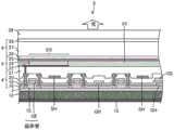
图3是表示一实施方式所涉及的显示器件的边缘区域及其附近的结构的剖视图。3 is a cross-sectional view showing the structure of the edge region and its vicinity of the display device according to the embodiment.
图4是表示一实施方式所涉及的显示器件中用于共同层的成膜的掩模的一示例的俯视图。4 is a plan view showing an example of a mask used for forming a common layer in the display device according to the embodiment.
图5是表示使用图4所示的掩模成膜一实施方式所涉及的显示器件中共通层的工序的图。5 is a diagram showing a process of forming a common layer in the display device according to the embodiment using the mask shown in FIG. 4 .
图6是示意性地示出了掩模间隔件与图4所示的掩模的开口端的关系的图。FIG. 6 is a diagram schematically showing a relationship between a mask spacer and an opening end of the mask shown in FIG. 4 .
图7的(a)是示意性地表示图4所示的掩模向像素区域侧偏移时的掩模的开口端和像素区域掩模间隔件的位置关系的俯视图,图7的(b)是示意性地表示图4所示的掩模中与边框区域的位于相邻的像素区域掩模间隔件间的凸部向夹着该凸部的像素区域掩模间隔件侧偏移时的掩模的开口端和像素区域掩模间隔件的位置关系的俯视图。(a) of FIG. 7 is a plan view schematically showing the positional relationship between the opening end of the mask and the mask spacer in the pixel area when the mask shown in FIG. 4 is shifted toward the pixel area side, and (b) of FIG. 7 It is a mask schematically showing the case where the convex portion between adjacent pixel region mask spacers in the frame region is shifted to the side of the pixel region mask spacer sandwiching the convex portion in the mask shown in FIG. 4 . A top view of the positional relationship between the opening end of the mold and the mask spacer in the pixel region.
图8的(a)是示意性地表示图4所示的掩模相对于像素区域掩模间隔件适当地配置时的掩模的开口端与像素区域掩模间隔件的位置关系的剖视图,图8的(b)是示意性地表示图8的(a)所示的掩模在像素区域DA侧偏离时的掩模的开口端和像素区域掩模间隔件的位置关系的剖视图。(a) of FIG. 8 is a cross-sectional view schematically showing the positional relationship between the opening end of the mask and the mask spacer in the pixel region when the mask shown in FIG. 4 is properly arranged with respect to the mask spacer in the pixel region. 8(b) is a cross-sectional view schematically showing the positional relationship between the opening end of the mask and the pixel region mask spacer when the mask shown in FIG. 8(a) is shifted toward the pixel region DA side.
图9是示出当图4所示的掩模向边框区域侧偏移时掩模的开口端与像素区域掩模间隔件的位置关系的俯视图。9 is a plan view showing the positional relationship between the opening end of the mask and the mask spacer in the pixel region when the mask shown in FIG. 4 is shifted toward the frame region side.
图10的(a)是示意性地表示,作为CMM在开口端使用具有俯视时具有直线形状的开口部的掩模,将该掩模适当地配置于像素区域掩模间隔件时的该掩模的开口部和像素区域掩模间隔件的位置关系的截面图,图10的(b)是示意性地表示图10的(a)所示的掩模向像素区域侧偏移时的该掩模的开口端与像素区域掩模间隔件的位置关系的截面图,图10的(c)是示意性地表示图10的(b)所示的状态下进行共通层的成膜后,由密封层密封时的问题点的截面图。(a) of FIG. 10 schematically shows a case where a mask having an opening having a linear shape in plan view is used as a CMM at the opening end, and the mask is appropriately placed on a pixel region mask spacer. 10 (b) is a schematic representation of the mask when the mask shown in (a) of FIG. 10 is shifted to the pixel area side. The cross-sectional view of the positional relationship between the opening end of the pixel area and the mask spacer in the pixel region. FIG. 10(c) schematically shows that after the common layer is formed in the state shown in FIG. A cross-sectional view of a problem spot when sealing.
图11是表示图10的(a)所示的掩模向边框区域侧偏移时的掩模的开口端与像素区域掩模间隔件的位置关系的俯视图。11 is a plan view showing the positional relationship between the opening end of the mask and the mask spacer in the pixel region when the mask shown in (a) of FIG. 10 is shifted toward the frame region side.
具体实施方式Detailed ways
详细说明本发明的一实施方式。另外,在以下各实施方式中与前面已经说明的部件具有相同功能的部件标注相同标记,不重复说明。One embodiment of the present invention will be described in detail. In addition, in each of the following embodiments, components having the same functions as those already described above are denoted by the same symbols, and the description thereof will not be repeated.
<显示器件的结构及制造方法的概要><Outline of Structure and Manufacturing Method of Display Device>
图1是表示本实施方式所涉及的显示器件2的制造方法的一示例流程图。图2是表示本实施方式所涉及的显示器件2的像素区域(显示区域)的结构的剖视图。图3是表示本实施方式所涉及的显示器件2的边缘区域NA及其附近的结构的剖视图。在以下的说明中,“同层”是指在同一工艺(成膜工序)中形成,“下层”是指在相较于比较对象的层之前的工艺中形成,“上层”是指在相较于比较对象的层之后的工艺中形成。FIG. 1 is a flowchart illustrating an example of a method of manufacturing a
在制造柔性显示器件的情况下,如图1~图3所示,首先,在透光性的支承基板(例如,母玻璃)上形成树脂层12(步骤S1)。接着,形成势垒层3(步骤S2)。接着,形成TFT层4(步骤S3)。接着,形成发光元件层5(步骤S4)。接着,形成密封层6(步骤S5)。接着,在密封层6上临时粘贴保护用的上表面膜(步骤S6)。When manufacturing a flexible display device, as shown in FIGS. 1 to 3 , first, a
接着,通过激光照射等使支承基板从树脂层12剥离(步骤S7)。接着,在树脂层12的下表面粘贴下表面膜10(步骤S8)。接着,将包括下表面膜10、树脂层12、势垒层3、TFT层4、发光元件层5、密封层6的层叠体切割,得到多个单片(步骤S9)。接着,从所得到的单片上剥离上表面膜后(步骤S10),粘贴功能膜39(步骤S11)。接着,在比形成有多个像素的像素区域DA(参照图3)更靠外侧(边框区域NA,参照图3)的一部分(端子部)安装电子电路基板(例如,IC芯片以及FPC)(步骤S12)。此外,步骤S1~S12由显示器件制造装置(包括进行步骤S1~S5的各工序的成膜装置)进行。Next, the support substrate is peeled from the
作为树脂层12的材料,例如可举出聚酰亚胺等。树脂层12的部分还能够通过两层树脂膜(例如聚酰亚胺膜)以及由它们夹着的无机绝缘膜取代。As a material of the
势垒层3是防止水、氧气等异物侵入TFT层4以及发光元件层5的层,例如能够由通过CVD法形成的氧化硅膜、氮化硅膜、或氮氧化硅膜、或者这些膜的层叠膜构成。The
TFT层4包括半导体膜15、比半导体膜15更上层的无机绝缘膜16(栅极绝缘膜)、比无机绝缘膜16更上层的栅电极GE和栅极布线GH、比栅电极GE和栅极布线GH更上层的无机绝缘膜18、比无机绝缘膜18更上层的电源布线CE、比电源布线CE更上层的无机绝缘膜20、比无机绝缘膜20更上层的源极布线SH以及比源极布线SH更上层的平坦化膜21(层间绝缘膜)。The
半导体层15例如由低温多晶硅(LTPS)或者氧化物半导体(例如In-Ga-Zn-O系的半导体)构成,并以包括半导体层15以及栅电极GE的方式构成晶体管(TFT)。图2中,晶体管以顶栅构造示出,但也可以是底栅构造。The
栅电极GE、栅极布线GH、电容电极CE以及源极布线SH例如由包括铝、钨、钼、钽、铬、钛、铜的至少一种的金属单层膜或层叠膜构成。图2的TFT层4包括一层半导体层以及三层金属层。The gate electrode GE, the gate wiring GH, the capacitor electrode CE, and the source wiring SH are composed of, for example, a metal single-layer film or laminated film including at least one of aluminum, tungsten, molybdenum, tantalum, chromium, titanium, and copper. The
无机绝缘膜16·18·20例如能够由通过CVD法形成的氧化硅(SiOx)膜或氮化硅(SiNx)膜或者这些膜的层叠膜构成。平坦化膜21可以由例如聚酰亚胺、丙烯酸等可涂布的感光性有机材料构成。The inorganic insulating
发光元件层5包括:比平坦化膜21更上层的阳极22、覆盖阳极22的边缘的绝缘性的边缘罩23、比边缘罩23更上层的EL(电致发光)层24、比EL层24更上层的阴极25以及掩模间隔件31·32。另外,发光元件层5可以在阴极25的更上层包括有机覆盖层、无机覆盖层等覆盖层。The light-emitting
边缘罩23例如通过在涂覆了聚酰亚胺、丙烯酸等有机材料后利用光刻进行图案化而形成。The
对于每个像素,发光元件ES(例如,OLED:有机发光二极管,QLED:量子点发光二极管)形成于发光元件层5,该发光元件ES包括阳极22、EL层24以及阴极25,控制发光元件ES的像素电路形成于TFT层4。For each pixel, a light emitting element ES (for example, OLED: Organic Light Emitting Diode, QLED: Quantum Dot Light Emitting Diode) is formed on the light emitting
阳极22是针对每个像素形成为岛状的图案电极。阴极25是共通地在全部像素上形成为整体的共用电极,不对每个像素涂覆,而是在整个像素区域DA上成膜。The
阳极22主要由溅射法形成,而阴极25主要由蒸镀法形成。在蒸镀形成阴极的情况下,作为蒸镀掩模,使用整个像素区域DA开口的被称为CMM(共通金属掩模)的开放掩模。The
EL层24作为功能层,例如通过从下层侧依次层叠空穴注入层、共通空穴传输层、岛状空穴传输层、发光层、空穴阻挡层、电子传输层、电子注入层而构成。发光层通过蒸镀法或喷墨法,例如在边缘罩23的开口(对每个子像素)以岛状形成。The
OLED的发光层使用蒸镀掩模例如FMM(精细金属掩模)进行蒸镀而形成为岛状的蒸镀层。QLED的发光层例如通过对使量子点扩散的溶剂进行喷墨涂覆而形成。另外,在OLED是白色发光类型的情况下,或者在形成多个像素共通的共通发光层的情况下,有时作为蒸镀掩模,使用被称为CMM(共通金属掩模)的开放掩模。The light-emitting layer of the OLED is vapor-deposited using a vapor-deposition mask such as FMM (Fine Metal Mask) to form an island-shaped vapor-deposition layer. The light emitting layer of the QLED is formed, for example, by inkjet coating a solvent that diffuses quantum dots. Also, when the OLED is a white light emitting type, or when a common light emitting layer common to a plurality of pixels is formed, an open mask called a CMM (Common Metal Mask) may be used as a deposition mask.
岛状空穴传输层通过使用FMM的蒸镀法形成为岛状蒸镀层。其他功能层通过使用FMM或CMM的蒸镀法形成为岛状或整体状的共通层。该些功能层可以是由有机材料构成的有机层,也可以是由无机材料构成的无机层。The island-shaped hole transport layer was formed as an island-shaped vapor-deposited layer by a vapor deposition method using FMM. Other functional layers are formed as island-shaped or monolithic common layers by vapor deposition using FMM or CMM. These functional layers may be organic layers made of organic materials, or inorganic layers made of inorganic materials.
覆盖层通过使用CMM的蒸镀法形成为整体状的共通层。覆盖层例如可以具有由有机材料构成的有机覆盖层和由无机材料构成的无机覆盖层依次层叠而成的层叠结构,也可以只设置其中一个。The cover layer is formed as an integral common layer by a vapor deposition method using a CMM. The covering layer may have, for example, a laminated structure in which an organic covering layer made of an organic material and an inorganic covering layer made of an inorganic material are sequentially laminated, or only one of them may be provided.
另外,也可以构成为不形成空穴注入层、共通空穴传输层、岛状空穴传输层、发光层、空穴阻挡层、电子传输层、电子注入层中的一层以上的层,进而形成其他层的构成也有可能。In addition, it is also possible to form one or more layers among the hole injection layer, the common hole transport layer, the island-like hole transport layer, the light emitting layer, the hole blocking layer, the electron transport layer, and the electron injection layer, and further Compositions that form other layers are also possible.
阳极22由例如ITO(Indium Tin Oxide)和Ag(银)或包括Ag的合金的层叠构成,并具有光反射性。阴极25能够由MgAg合金(极薄膜)、ITO、IZO(Indium zinc Oxide)等透光性的导电材料构成。The
在发光元件ES为OLED的情况下,通过阳极22以及阴极25之间的驱动电流使空穴和电子在发光层内复合,由此产生的激子向基态迁移的过程中放出光。阴极25是透光性的,阳极22是光反射性的,因此从EL层24放出的光朝向上方,成为顶部发光。阴极25是光反射性的,阳极22是透光性的,因此从EL层24放出的光朝向下方,成为底部发光。When the light-emitting element ES is an OLED, holes and electrons are recombined in the light-emitting layer by a driving current between the
在发光元件ES为QLED的情况下,通过阳极22以及阴极25之间的驱动电流使空穴和电子在发光层内复合,由此产生的激子从量子点的导带能级(conduction band)向价带能级(valence band)转变的过程中放出光(荧光)。In the case where the light-emitting element ES is a QLED, the driving current between the
也可以在发光元件层5形成除上述的OLED、QLED以外的发光元件ES(无机发光二极管等)。Light-emitting elements ES (inorganic light-emitting diodes, etc.) other than the above-mentioned OLEDs and QLEDs may also be formed on the light-emitting
如图3所示,掩模间隔件31是设置在像素区域DA内的像素区域掩模间隔件。掩模间隔件32是设置在包围像素区域DA的边框区域NA中的边框区域掩模间隔件。掩模间隔件31设置在各像素中相邻的阳极露出部分(露出阳极22的边缘罩23的开口)之间。另外,在像素区域DA中,可以以包围显示像素的方式设置虚拟像素,也可以仅设置显示像素。显示像素中的阳极露出部分作为发光元件ES的发光区域发挥功能。更具体地说,在边缘罩23的规定部分中,在阴极25侧(即,TFT层4的相反侧)突出地设置掩模间隔件31。在图2中,省略了掩模间隔件31的图示。As shown in FIG. 3 , the
掩模间隔件31在由FMM成膜时定位FMM。掩模间隔件32在由FMM成膜时定位FMM,同时由CMM成膜时定位CMM。因此,FMM在成膜时(换言之,在与被成膜基板紧密接触时)由掩模间隔件31·32定位。因此,CMM在成膜时(换言之,在与被成膜基板紧密接触时)由掩模间隔件32定位。The
掩模间隔件31·32例如由感光性树脂材料形成。掩模间隔件31·32可以由与边缘罩23相同的材料形成,也可以由不同的材料形成。The
密封层6具有透光性,且包含覆盖阴极25的无机密封膜26、比无机密封膜26更上层的有机缓冲膜27、比有机缓冲膜27更上层的无机密封膜28。覆盖发光元件层5的密封层6防止水、氧等异物向发光元件层5渗透。The
无机密封层26和无机密封层28分别是无机绝缘膜,可以由例如通过CVD法形成的氧化硅膜、氮化硅膜或氮氧化硅膜、或这些层的层叠膜构成。有机缓冲膜27是具有平坦化效果的透光性有机膜,可以由例如丙烯酸等可涂布的有机材料构成。有机缓冲膜27例如能够通过喷墨涂覆形成。如图3所示,在边框区域NA中,可以设置用于停止喷墨的液滴的框状的堤部33和包围该堤部33的未图示的框状的堤部。堤部33可以用与边缘罩23、掩模间隔件31·32相同的材料同时形成。另外,包围堤部33的未图示的框状的堤部例如具有下层和上层的双层结构。上述下层在形成平坦化膜21的图案时,可以用与平坦化膜21相同的材料同时形成。上述上层例如在形成边缘罩23、掩模间隔件31·32时,可以用与这些边缘罩23、掩模间隔件31·32相同的材料同时形成。The
下表面膜10是例如PET膜,因此通过在剥离了支承基板后粘贴于树脂层12的下表面而实现柔软性优异的显示器件。功能膜39例如具有光学补偿功能、触摸传感器功能、保护功能的至少一种。Since the
以上对柔性显示器件进行了说明,但在制造非柔性显示器件的情况下,通常不需要树脂层的形成、基材的替换等,因此例如在玻璃基板上进行步骤S2~S5的层叠工序,之后转移至步骤S9。The flexible display device has been described above, but in the case of manufacturing a non-flexible display device, the formation of the resin layer, the replacement of the base material, etc. are generally not required, so for example, the lamination process of steps S2 to S5 is performed on a glass substrate, and then Transfer to step S9.
如上所述,本实施方式所涉及的显示器件2对于全部像素(即,多个像素)具有至少一层共通层,该共通层在整个像素区域DA上形成整体状。As described above, the
图4是示出本实施方式所涉及的显示器件2中的共通层的成膜的掩模71的一示例的俯视图。图5是表示使用图4所示的掩模71成膜一实施方式所涉及的显示器件2中共通层41的工序的图。FIG. 4 is a plan view showing an example of a
如上所述,掩模71是被称为CMM的开放掩模,用于成膜全部像素共通的共通层。如图4和图5所示,掩模71包括开口部72,开口部72开口整个像素区域DA,该像素区域DA至少包括设置有显示像素的显示区域。As described above, the
另外,在图4中,如上所述,可以在作为母板的支撑基板上,在步骤S9中对被单片化的多个显示器件2的像素区域DA设置有一个掩模71,也可以仅设置有一个开口部72。In addition, in FIG. 4, as described above, one
如图4和图5所示,在开口部72的开口端72a中,设置有俯视时反复设置有凹部和凸部的凹凸部73。如图5所示,凹凸部73的间隔(周期),换言之,在凹凸部73中相邻的凸部间的间隔以及相邻的凹部间的间隔,例如与掩模间隔件31的间隔(相邻的掩模间隔件31之间的距离)相等。另外,掩模间隔件32的间隔(相邻的掩模间隔件32之间的距离)小于掩模间隔件31的间隔。在图5所示的例子中,以掩模间隔件31的间隔的一半的间隔形成掩模间隔件32。掩模间隔件31形成为例如,与FMM的接触面的上表面直径为5~10μm的圆形,且高度为1.0~2.0μm的具有锥形的圆柱形。掩模间隔件31形成为例如,与FMM与CMM的接触面的上表面以便为10~15μm的四边形(例如,正方形)且高度为1.0~2.0μm的具有锥形的四棱柱形。另外,在此,掩模间隔件31·32的高度以平坦化膜21的上表面为基准,表示为从该平坦化膜21的上表面开始的高度。As shown in FIGS. 4 and 5 , the opening
开口部72的开口端72a(换言之,凹凸部73)形成为适合于掩模间隔件31的配置的波形形状,使得该开口端72a和掩模间隔件31具有一定以上的距离。凹凸部73形成为当掩模71与被成膜基板重叠时,该凹凸部73的凸部位于与边框区域NA相邻的掩模间隔件31之间。Opening
因此,在与被成膜基板紧密接触时,掩模71被配置为使凹凸部73的凸部位于与边框区域NA相邻的掩模间隔件31之间,并且在掩模71被适当地相对于掩模间隔件31配置的情况下,如图5所示,凹凸部73与相邻于边框区域NA的掩模间隔件31具有一定以上的距离。Therefore, when in close contact with the substrate to be filmed, the
共通层41形成在掩模71的开口部72上。因此,在俯视时,在共通层41的端部具有与掩模71的凹凸部73对应的凹凸部42。即,在共通层41的端部设置有沿着凹凸部73的凸部与该凸部相对的凹部、以及沿着凹凸部73的凹部与该凹部相对的凸部。因此,凹凸部42具有与凹凸部73对应的例如波形形状。凹凸部42的间隔与凹凸部73的间隔相同,与掩模间隔件31的间隔相等。共通层41与多个像素共通地成膜在掩模间隔件31上,使得该凹凸部42的凹部位于与边框区域NA相邻的掩模间隔件31之间。The
本实施方式所涉及的显示器件2的制造方法包括:以包围像素区域DA的方式在该像素区域DA的外侧的边框区域NA中形成多个掩模间隔件32的工序;在像素区域DA内形成多个掩模间隔件31的工序;在像素区域DA内开口,使具有开口部72的掩模71接触于掩模间隔件31,该开口部72具有在俯视时设置了凹凸部73的开口端72a,在该些多个掩模间隔件31上形成与多个像素共通的共通层41的工序。The manufacturing method of the
根据本实施方式,即使在掩模71与被成膜基板紧密接触时掩模71的位置偏离,掩模71的开口端72a与掩模间隔件31不接触,能够防止异物的附着。According to this embodiment, even if the position of the
但是,凹凸部73的形状不限于波形形状,只要像素区域DA内的掩模间隔件31和该凹凸部73(换言之,掩模71的开口端72a)之间的距离保持在一定以上即可。However, the shape of the concave-
为了均匀地定位FMM,用与先前相同的布置形成掩模间隔件31。在本实施方式中,通过不变更先前的掩模间隔件31的配置,而变更掩模71的开口端72a的形状,来制造比现有更可靠的显示器件2。In order to uniformly position the FMMs,
另外,对于边框区域NA的掩模间隔件32,也可以以使与凹凸部73(开口端72a)之间的距离保持一定以上的方式配置有该掩模间隔件32。In addition, the
图6是示意性地示出了掩模间隔件31和图4所示的掩模71的开口端72a之间的关系的图。在图6中,假设以如下方式形成波形,即,将掩模间隔件31的直径设为d1,使得掩模71的开口端72a与相对于该开口端72a的掩模间隔件31的端部的距离为距离d2。在这种情况下,凹凸部73的凹部成为具有由d2+d1/2表示的半径R的圆的圆弧。此处,例如,假设d1=10μm,考虑到掩模71的加工精度和掩模偏差,并且如果d2=50μm,则R=50+10/2=55μm。FIG. 6 is a diagram schematically showing the relationship between the
掩模71通过使用光刻和蚀刻处理从其表里两面侧蚀刻来进行图案化。即使光光刻的曝光分辨率是3μm(ghi线),上述波形形状在尺寸上也足够大,能够容易地精细加工为上述波形形状。The
以下,参照图7的(a)·(b)~图11,更详细地说明利用掩模71成膜共通层而所产生的效果。Hereinafter, the effect of forming a common layer using the
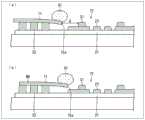
图7的(a)是示意性地表示图4所示的掩模71向像素区域DA侧偏移时的掩模71的开口端72a和掩模间隔件31的位置关系的俯视图,图7的(b)是示意性地表示图4所示的掩模71中、位于与边框区域NA的相邻的掩模间隔件31间的凸部向夹着该凸部的掩模间隔件31侧偏移时的掩模71的开口端72a和掩模间隔件31的位置关系的俯视图。(a) of FIG. 7 is a plan view schematically showing the positional relationship between the opening
图8的(a)是示意性地表示图4所示的掩模71相对于掩模间隔件31适当地配置时的掩模71的开口端72a与掩模间隔件31的位置关系的剖视图,图8的(b)是示意性地表示图8的(a)所示的掩模71在像素区域DA侧偏离时的掩模71的开口端72a和掩模间隔件31的位置关系的剖视图。(a) of FIG. 8 is a cross-sectional view schematically showing the positional relationship between the opening
另外,图10的(a)是示意性地表示,作为CMM使用开口端82a在俯视时具有直线形状的开口部82的掩模81代替掩模71的情况下,将掩模81适当地配置于掩模间隔件31时的掩模81的开口部82和掩模间隔件31的位置关系的截面图,图10的(b)是示意性地表示图10的(a)所示的掩模81向像素区域DA侧偏移时的掩模81的开口端82a与掩模间隔件31的位置关系的截面图,图10的(c)是示意性地表示图10的(b)所示的状态下进行共通层(未图示)的成膜后,由密封层6密封时的问题点的截面图。In addition, Fig. 10 (a) schematically shows that when using a
在掩模71的开口端72a和掩模81的开口端82a,特别是掩模71·81是构成EL层24中的各功能层(例如有机膜)的CMM的情况下,该些掩模71·81的开口端72a·82a位于包括虚拟像素的像素区域DA的周边端。如图8的(a)和图10的(a)所示,在掩模71·81的开口端72a·82a上有时附着有由成膜而沉积的成膜材料构成的膜、经掩模清洗而无法去除的残留物等异物91。In the case where the opening
共通层41成膜时,被成膜基板和掩模71·81例如在被成膜基板的背面侧配置磁体(磁铁板)等磁力发生源,用磁铁吸引容易弯曲的掩模71·81的中央部,掩模71·81和被成膜基板之间的间隙消失后,由磁力紧密接触。When the
与FMM相比,掩模71·81的开口面积大,并且,在与被成膜基板紧密接触时,仅由设置在边框区域NA中的掩模间隔件32来定位掩模71·81。The
因此,在使这些掩模71·81与被成膜基板紧密接触时产生了位置偏差的情况下,与FMM相比,掩模71·81的开口端72a·82a容易因自重或磁力而向被成膜基板侧弯曲。Therefore, when these
因此,在使掩模81与被成膜基板紧密接触时,如果掩模81因磁力而从图10的(a)所示的状态偏离到如图10的(b)所示的像素区域DA侧,则向被成膜基板侧弯曲的开口端82a接触到掩模间隔件31。其结果,附着在开口端82a上的异物91被转印到掩模间隔件31上。Therefore, when the
此处,例如,共通层41如上述那样是EL层24的功能层(例如有机膜),在形成共通层41之后,如图10的(c)所示,由密封层6密封包含上述共通层41的发光元件层5的情况为例进行考察。Here, for example, the
在用密封层6密封发光元件层5的情况下,如图10的(c)所示,如果在高的掩模间隔件31上附着有更高的异物91,则不能用密封层6适当地覆盖异物91,从而产生密封层6的缺损。该缺损成为水分渗透路径,水分从该缺损中渗透,当到达发光元件ES时,产生黑点。其结果,使用如上所述的掩模81制造的显示器件的可靠性降低。In the case of sealing the light-emitting
然而,根据本实施方式,例如在掩模71的开口端72a上形成波形形状的凹凸部73,使得掩模71的开口端72a与掩模31之间的距离以一定以上分离。另外,图8的(a)所示的掩模71的开口端72a与掩模间隔件31之间的距离g(g=R=d2+d1/2)被设计为考虑了掩模精度和掩模偏差之后的距离。因此,如图7的(a)·(b)和图8的(b)所示,即使掩模71相对于掩模间隔件31的位置偏离,开口端72a与掩模间隔件31也不接触。因此,根据本实施方式,能够抑制来自掩模71的异物91的剥离,其结果,密封层6无法覆盖的异物91减少,提高了显示装置的可靠性,并且能够改善成品率。However, according to the present embodiment, for example, the wave-shaped concave-
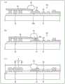
另外,图9是示出当图4所示的掩模71向边框区域NA侧偏移时掩模71的开口端72a与掩模间隔件31的位置关系的俯视图。图11是表示图10的(a)所示的掩模81向边框区域NA侧偏移时的掩模81的开口端82a与掩模间隔件31的位置关系的俯视图。9 is a plan view showing the positional relationship between the opening
如图11所示,在使用掩模81作为CMM的情况下,如果开口端82a向边框区域NA侧偏移,则掩模81的开口端72a为直线状,因此与开口端72a接触的掩模间隔件32的数量较多,异物91附着于掩模间隔件32的可能性提高。As shown in FIG. 11, in the case of using the
另外,如图3所示,有时在掩模间隔件31和掩模间隔件32之间设置有沟道21a,该沟道21a成为阴极25与设置在TFT层4上的布线DW的接触区域。In addition, as shown in FIG. 3 , a
在这种情况下,如图11所示,当掩模81的开口端82a向边框区域NA侧偏移时,由掩模81形成的共通层41均匀地超出边框区域NA而成膜。其结果,共通层41均匀地堵塞在沟道21a内,阴极25和布线DW无法接触的区域的面积变大。In this case, as shown in FIG. 11 , when the opening
然而,当开口端72a如掩模71那样具有凹凸部73时,如图9所示,即使开口端72a与图11所示的掩模81的开口端82a向边框区域NA侧的偏移相同,与该开口端72a接触的掩模间隔件32的数量与开口端82a偏离到边框区域NA侧的情况相比变少。因此,通过使用掩模71作为CMM,与作为CMM而使用掩模81的情况相比,能够抑制异物91附着到掩模间隔件32上。However, when the opening
另外,如图9所示,根据本实施方式,由于共通层41的端部具有与凹凸部73对应的凹凸部42,所以即使在边框区域NA形成了凹凸部42的至少一部分的情况下,也比使用CMM掩模81的情况,共通层41侵入到沟道21a内的面积小,阴极25和布线DW无法接触的区域的面积小。In addition, as shown in FIG. 9, according to the present embodiment, since the end portion of the
因此,根据本实施方式,能够在确保掩模71的开口端72a和掩模间隔件31的余量的同时,确保阴极25和布线DW的接触区域。因此,根据本实施方式,可以提供一种比现有可靠性更高的显示器件2以及能够制造比现有可靠性更高的显示器件2的掩模71和显示器件2的制造方法。Therefore, according to the present embodiment, it is possible to ensure a contact area between the
另外,根据本实施方式,如果是不对每个像素进行涂覆而是在像素区域DA整体上成膜的层,则成为由掩模71成膜的共通层41的对象。作为上述共通层41,例如可举出空穴注入层、共通空穴传输层、空穴阻挡层、电子传输层和电子注入层等之类的EL层24中的功能层(有机层或无机层)。另外,如上所述,当发光元件ES是例如白色发光的OLED或是具有对多个像素共通的共通发光层的OLED的情况下,在发光层的成膜中使用CMM的情况下,发光层也成为上述共通层41的对象。另外,在以与上述功能层相同的尺寸形成覆盖层的情况下,覆盖层也成为上述共用层41的对象。另外,对于阴极25,在边框区域NA形成所述接触区域的边未成为对象,但是在没有所述接触区域的情况下(没有所述接触区域的边),成为掩模71的成膜的对象。In addition, according to the present embodiment, if the layer is formed over the entire pixel area DA without coating for each pixel, it becomes the object of the
在图4中,以在掩模71的全部开口端72a上形成有凹凸部73的情况为例进行图示,但是,如果在掩模71的开口端72a上设置有凹凸部73,也可以将凹凸部73设置在掩模71的开口端72a的一部分。也就是说,可以将凹凸部73设置在掩模71的开口端72a的至少一部分(至少一条边)。In FIG. 4 , the case where the concave-
本发明不限于上述各实施方式,能在权利要求所示的范围中进行各种变更,将在不同的实施方式中分别公开的技术手段适当组合而得到的实施方式也包含于本发明的技术范围。而且,能够通过组合各实施方式分别公开的技术方法来形成新的技术特征。The present invention is not limited to the above-mentioned embodiments, and various changes can be made within the range shown in the claims. Embodiments obtained by appropriately combining technical means disclosed in different embodiments are also included in the technical scope of the present invention. . Furthermore, new technical features can be formed by combining the technical means disclosed in the respective embodiments.
附图标记说明Explanation of reference signs
2显示器件2 display devices
21a 沟道(接触区域)21a Channel (contact area)
24 EL层24 EL layers
25 阴极25 Cathode
31 掩模间隔件(像素区域掩模间隔件)31 mask spacer (pixel area mask spacer)
32 掩模间隔件(边框区域掩模间隔件)32 mask spacers (bezel area mask spacers)
41 共通层41 common floor
42、73 凹凸部42, 73 concave and convex part
71 掩模71 mask
72 开口部72 opening
72a 开口端72a Open end
DA 像素区域DA pixel area
NA 边框区域NA border area
Claims (10)
Translated fromChineseApplications Claiming Priority (1)
| Application Number | Priority Date | Filing Date | Title |
|---|---|---|---|
| PCT/JP2018/013966WO2019187148A1 (en) | 2018-03-30 | 2018-03-30 | Display device, mask, and method for manufacturing display device |
Publications (2)
| Publication Number | Publication Date |
|---|---|
| CN111937494A CN111937494A (en) | 2020-11-13 |
| CN111937494Btrue CN111937494B (en) | 2023-06-16 |
Family
ID=68059785
Family Applications (1)
| Application Number | Title | Priority Date | Filing Date |
|---|---|---|---|
| CN201880091862.6AActiveCN111937494B (en) | 2018-03-30 | 2018-03-30 | Display device and method for manufacturing display device |
Country Status (3)
| Country | Link |
|---|---|
| US (1) | US12161021B2 (en) |
| CN (1) | CN111937494B (en) |
| WO (1) | WO2019187148A1 (en) |
Families Citing this family (5)
| Publication number | Priority date | Publication date | Assignee | Title |
|---|---|---|---|---|
| WO2021250749A1 (en)* | 2020-06-08 | 2021-12-16 | シャープ株式会社 | Display device and display device manufacturing method |
| CN112909205A (en)* | 2021-02-03 | 2021-06-04 | 武汉华星光电半导体显示技术有限公司 | Display panel, preparation method thereof and display device |
| JP2022175716A (en)* | 2021-05-14 | 2022-11-25 | 株式会社ジャパンディスプレイ | Display device |
| WO2022252005A1 (en)* | 2021-05-31 | 2022-12-08 | 京东方科技集团股份有限公司 | Display panel and display apparatus |
| US20230271445A1 (en)* | 2022-02-25 | 2023-08-31 | Intel Corporation | Reusable composite stencil for spray processes |
Citations (11)
| Publication number | Priority date | Publication date | Assignee | Title |
|---|---|---|---|---|
| CN1750719A (en)* | 2004-09-17 | 2006-03-22 | 株式会社半导体能源研究所 | Display device and manufacturing method thereof |
| CN1825616A (en)* | 2004-09-29 | 2006-08-30 | 株式会社半导体能源研究所 | Display device, electronic device, and method for manufacturing the display device |
| JP2007234248A (en)* | 2006-02-27 | 2007-09-13 | Kyocera Corp | Vapor deposition mask and organic EL display manufacturing method using the same |
| JP2007258336A (en)* | 2006-03-22 | 2007-10-04 | Toray Ind Inc | Mask for thin film patterning and its manufacturing method |
| JP2011222146A (en)* | 2010-04-05 | 2011-11-04 | Canon Inc | Method of manufacturing organic el display device |
| JP2013089475A (en)* | 2011-10-19 | 2013-05-13 | Canon Inc | Light-emitting display device and method for manufacturing the same |
| JP2014026906A (en)* | 2012-07-30 | 2014-02-06 | Canon Inc | Display device and manufacturing method therefor |
| JP2014041740A (en)* | 2012-08-22 | 2014-03-06 | Canon Inc | Display device and manufacturing method of the same |
| CN106567052A (en)* | 2016-10-24 | 2017-04-19 | 武汉华星光电技术有限公司 | Mask plate and encapsulating method for OLED device |
| CN107740040A (en)* | 2017-09-08 | 2018-02-27 | 上海天马有机发光显示技术有限公司 | Mask plate component and evaporation coating device |
| CN107845667A (en)* | 2017-11-01 | 2018-03-27 | 上海天马微电子有限公司 | Organic light-emitting display panel, display device and manufacturing method thereof |
Family Cites Families (3)
| Publication number | Priority date | Publication date | Assignee | Title |
|---|---|---|---|---|
| JP2009259404A (en) | 2008-04-11 | 2009-11-05 | Sharp Corp | Organic el display device and method for manufacturing same |
| KR20150025994A (en)* | 2013-08-30 | 2015-03-11 | 엘지디스플레이 주식회사 | Organic light emitting diode display device and method of fabricating the same |
| JP7017032B2 (en)* | 2016-06-28 | 2022-02-08 | 大日本印刷株式会社 | A vapor deposition mask, a method for manufacturing an organic semiconductor device, and a method for manufacturing an organic EL display. |
- 2018
- 2018-03-30CNCN201880091862.6Apatent/CN111937494B/enactiveActive
- 2018-03-30USUS17/042,835patent/US12161021B2/enactiveActive
- 2018-03-30WOPCT/JP2018/013966patent/WO2019187148A1/ennot_activeCeased
Patent Citations (11)
| Publication number | Priority date | Publication date | Assignee | Title |
|---|---|---|---|---|
| CN1750719A (en)* | 2004-09-17 | 2006-03-22 | 株式会社半导体能源研究所 | Display device and manufacturing method thereof |
| CN1825616A (en)* | 2004-09-29 | 2006-08-30 | 株式会社半导体能源研究所 | Display device, electronic device, and method for manufacturing the display device |
| JP2007234248A (en)* | 2006-02-27 | 2007-09-13 | Kyocera Corp | Vapor deposition mask and organic EL display manufacturing method using the same |
| JP2007258336A (en)* | 2006-03-22 | 2007-10-04 | Toray Ind Inc | Mask for thin film patterning and its manufacturing method |
| JP2011222146A (en)* | 2010-04-05 | 2011-11-04 | Canon Inc | Method of manufacturing organic el display device |
| JP2013089475A (en)* | 2011-10-19 | 2013-05-13 | Canon Inc | Light-emitting display device and method for manufacturing the same |
| JP2014026906A (en)* | 2012-07-30 | 2014-02-06 | Canon Inc | Display device and manufacturing method therefor |
| JP2014041740A (en)* | 2012-08-22 | 2014-03-06 | Canon Inc | Display device and manufacturing method of the same |
| CN106567052A (en)* | 2016-10-24 | 2017-04-19 | 武汉华星光电技术有限公司 | Mask plate and encapsulating method for OLED device |
| CN107740040A (en)* | 2017-09-08 | 2018-02-27 | 上海天马有机发光显示技术有限公司 | Mask plate component and evaporation coating device |
| CN107845667A (en)* | 2017-11-01 | 2018-03-27 | 上海天马微电子有限公司 | Organic light-emitting display panel, display device and manufacturing method thereof |
Also Published As
| Publication number | Publication date |
|---|---|
| US20210028256A1 (en) | 2021-01-28 |
| CN111937494A (en) | 2020-11-13 |
| US12161021B2 (en) | 2024-12-03 |
| WO2019187148A1 (en) | 2019-10-03 |
Similar Documents
| Publication | Publication Date | Title |
|---|---|---|
| CN111937494B (en) | Display device and method for manufacturing display device | |
| US10516012B2 (en) | Electro-optical device and manufacturing method thereof | |
| CN104733495B (en) | Organic light-emitting diode (OLED) display apparatus and its manufacture method | |
| US11626449B2 (en) | Display device and method for producing display device | |
| CN111937058B (en) | Display device | |
| US11653547B2 (en) | Display device | |
| CN112513959B (en) | Display device | |
| KR102169862B1 (en) | Organic light emitting diode display device and fabricating method thereof | |
| WO2019187139A1 (en) | Display device | |
| WO2020021654A1 (en) | Display device | |
| WO2019167113A1 (en) | Display panel | |
| WO2020202525A1 (en) | Display device | |
| US11114522B2 (en) | Display device, manufacturing method of display device, and exposure device | |
| WO2020021722A1 (en) | Method for manufacturing display device | |
| CN111902855A (en) | Method for manufacturing display device and display device | |
| US20200091258A1 (en) | Display device, display device production method, display device production apparatus, and controller | |
| WO2020202274A1 (en) | Display device, and method for manufacturing display device | |
| CN111919510B (en) | display screen | |
| WO2019064560A1 (en) | Display device, method for manufacturing display device, and manufacturing device for display device | |
| CN114038864A (en) | Display substrate, manufacturing method thereof and display panel | |
| US10777633B2 (en) | Display device, display device manufacturing method, and display device manufacturing apparatus | |
| WO2020039591A1 (en) | Display device | |
| US11968866B2 (en) | Display device | |
| WO2023105599A1 (en) | Display device | |
| WO2019186897A1 (en) | Substrate for foreign object removal and method for manufacturing display device |
Legal Events
| Date | Code | Title | Description |
|---|---|---|---|
| PB01 | Publication | ||
| PB01 | Publication | ||
| SE01 | Entry into force of request for substantive examination | ||
| SE01 | Entry into force of request for substantive examination | ||
| GR01 | Patent grant | ||
| GR01 | Patent grant |