CN111937127A - Material-reduced metal plates on power semiconductor chips - Google Patents
Material-reduced metal plates on power semiconductor chipsDownload PDFInfo
- Publication number
- CN111937127A CN111937127ACN201980024501.4ACN201980024501ACN111937127ACN 111937127 ACN111937127 ACN 111937127ACN 201980024501 ACN201980024501 ACN 201980024501ACN 111937127 ACN111937127 ACN 111937127A
- Authority
- CN
- China
- Prior art keywords
- power semiconductor
- metal plate
- central portion
- metal
- boundary
- Prior art date
- Legal status (The legal status is an assumption and is not a legal conclusion. Google has not performed a legal analysis and makes no representation as to the accuracy of the status listed.)
- Granted
Links
- 229910052751metalInorganic materials0.000titleclaimsabstractdescription145
- 239000002184metalSubstances0.000titleclaimsabstractdescription144
- 239000004065semiconductorSubstances0.000titleclaimsabstractdescription107
- 239000000463materialSubstances0.000titledescription7
- 239000000758substrateSubstances0.000claimsabstractdescription27
- 239000007769metal materialSubstances0.000claimsabstractdescription25
- 238000001465metallisationMethods0.000claimsabstractdescription25
- 238000000034methodMethods0.000claimsdescription20
- 238000005530etchingMethods0.000claimsdescription11
- 238000004519manufacturing processMethods0.000claimsdescription6
- 239000010949copperSubstances0.000description13
- HBMJWWWQQXIZIP-UHFFFAOYSA-Nsilicon carbideChemical compound[Si+]#[C-]HBMJWWWQQXIZIP-UHFFFAOYSA-N0.000description5
- 229910010271silicon carbideInorganic materials0.000description4
- 238000005245sinteringMethods0.000description4
- 238000005382thermal cyclingMethods0.000description4
- 230000000930thermomechanical effectEffects0.000description4
- 229910052802copperInorganic materials0.000description3
- 238000003466weldingMethods0.000description3
- 239000004020conductorSubstances0.000description2
- 230000001419dependent effectEffects0.000description2
- 238000003754machiningMethods0.000description2
- 229910052750molybdenumInorganic materials0.000description2
- 239000002105nanoparticleSubstances0.000description2
- 229910052709silverInorganic materials0.000description2
- RYGMFSIKBFXOCR-UHFFFAOYSA-NCopperChemical compound[Cu]RYGMFSIKBFXOCR-UHFFFAOYSA-N0.000description1
- ZOKXTWBITQBERF-UHFFFAOYSA-NMolybdenumChemical compound[Mo]ZOKXTWBITQBERF-UHFFFAOYSA-N0.000description1
- XUIMIQQOPSSXEZ-UHFFFAOYSA-NSiliconChemical compound[Si]XUIMIQQOPSSXEZ-UHFFFAOYSA-N0.000description1
- BQCADISMDOOEFD-UHFFFAOYSA-NSilverChemical compound[Ag]BQCADISMDOOEFD-UHFFFAOYSA-N0.000description1
- 230000009286beneficial effectEffects0.000description1
- 230000015556catabolic processEffects0.000description1
- 239000000919ceramicSubstances0.000description1
- 238000006731degradation reactionMethods0.000description1
- 238000005516engineering processMethods0.000description1
- 239000011859microparticleSubstances0.000description1
- 239000011733molybdenumSubstances0.000description1
- 238000004806packaging method and processMethods0.000description1
- 239000002245particleSubstances0.000description1
- 230000002093peripheral effectEffects0.000description1
- 238000004080punchingMethods0.000description1
- 229910052710siliconInorganic materials0.000description1
- 239000010703siliconSubstances0.000description1
- 239000004332silverSubstances0.000description1
- 238000004088simulationMethods0.000description1
Images


Classifications
- H—ELECTRICITY
- H01—ELECTRIC ELEMENTS
- H01L—SEMICONDUCTOR DEVICES NOT COVERED BY CLASS H10
- H01L24/00—Arrangements for connecting or disconnecting semiconductor or solid-state bodies; Methods or apparatus related thereto
- H01L24/01—Means for bonding being attached to, or being formed on, the surface to be connected, e.g. chip-to-package, die-attach, "first-level" interconnects; Manufacturing methods related thereto
- H01L24/42—Wire connectors; Manufacturing methods related thereto
- H01L24/47—Structure, shape, material or disposition of the wire connectors after the connecting process
- H01L24/49—Structure, shape, material or disposition of the wire connectors after the connecting process of a plurality of wire connectors
- H—ELECTRICITY
- H01—ELECTRIC ELEMENTS
- H01L—SEMICONDUCTOR DEVICES NOT COVERED BY CLASS H10
- H01L23/00—Details of semiconductor or other solid state devices
- H01L23/34—Arrangements for cooling, heating, ventilating or temperature compensation ; Temperature sensing arrangements
- H01L23/36—Selection of materials, or shaping, to facilitate cooling or heating, e.g. heatsinks
- H01L23/373—Cooling facilitated by selection of materials for the device or materials for thermal expansion adaptation, e.g. carbon
- H01L23/3735—Laminates or multilayers, e.g. direct bond copper ceramic substrates
- H—ELECTRICITY
- H01—ELECTRIC ELEMENTS
- H01L—SEMICONDUCTOR DEVICES NOT COVERED BY CLASS H10
- H01L21/00—Processes or apparatus adapted for the manufacture or treatment of semiconductor or solid state devices or of parts thereof
- H01L21/02—Manufacture or treatment of semiconductor devices or of parts thereof
- H01L21/04—Manufacture or treatment of semiconductor devices or of parts thereof the devices having potential barriers, e.g. a PN junction, depletion layer or carrier concentration layer
- H01L21/48—Manufacture or treatment of parts, e.g. containers, prior to assembly of the devices, using processes not provided for in a single one of the groups H01L21/18 - H01L21/326 or H10D48/04 - H10D48/07
- H01L21/4814—Conductive parts
- H01L21/4871—Bases, plates or heatsinks
- H—ELECTRICITY
- H01—ELECTRIC ELEMENTS
- H01L—SEMICONDUCTOR DEVICES NOT COVERED BY CLASS H10
- H01L23/00—Details of semiconductor or other solid state devices
- H01L23/562—Protection against mechanical damage
- H—ELECTRICITY
- H01—ELECTRIC ELEMENTS
- H01L—SEMICONDUCTOR DEVICES NOT COVERED BY CLASS H10
- H01L24/00—Arrangements for connecting or disconnecting semiconductor or solid-state bodies; Methods or apparatus related thereto
- H01L24/01—Means for bonding being attached to, or being formed on, the surface to be connected, e.g. chip-to-package, die-attach, "first-level" interconnects; Manufacturing methods related thereto
- H01L24/42—Wire connectors; Manufacturing methods related thereto
- H01L24/47—Structure, shape, material or disposition of the wire connectors after the connecting process
- H01L24/48—Structure, shape, material or disposition of the wire connectors after the connecting process of an individual wire connector
- H—ELECTRICITY
- H01—ELECTRIC ELEMENTS
- H01L—SEMICONDUCTOR DEVICES NOT COVERED BY CLASS H10
- H01L2224/00—Indexing scheme for arrangements for connecting or disconnecting semiconductor or solid-state bodies and methods related thereto as covered by H01L24/00
- H01L2224/01—Means for bonding being attached to, or being formed on, the surface to be connected, e.g. chip-to-package, die-attach, "first-level" interconnects; Manufacturing methods related thereto
- H01L2224/02—Bonding areas; Manufacturing methods related thereto
- H01L2224/04—Structure, shape, material or disposition of the bonding areas prior to the connecting process
- H01L2224/04026—Bonding areas specifically adapted for layer connectors
- H—ELECTRICITY
- H01—ELECTRIC ELEMENTS
- H01L—SEMICONDUCTOR DEVICES NOT COVERED BY CLASS H10
- H01L2224/00—Indexing scheme for arrangements for connecting or disconnecting semiconductor or solid-state bodies and methods related thereto as covered by H01L24/00
- H01L2224/01—Means for bonding being attached to, or being formed on, the surface to be connected, e.g. chip-to-package, die-attach, "first-level" interconnects; Manufacturing methods related thereto
- H01L2224/02—Bonding areas; Manufacturing methods related thereto
- H01L2224/04—Structure, shape, material or disposition of the bonding areas prior to the connecting process
- H01L2224/04042—Bonding areas specifically adapted for wire connectors, e.g. wirebond pads
- H—ELECTRICITY
- H01—ELECTRIC ELEMENTS
- H01L—SEMICONDUCTOR DEVICES NOT COVERED BY CLASS H10
- H01L2224/00—Indexing scheme for arrangements for connecting or disconnecting semiconductor or solid-state bodies and methods related thereto as covered by H01L24/00
- H01L2224/01—Means for bonding being attached to, or being formed on, the surface to be connected, e.g. chip-to-package, die-attach, "first-level" interconnects; Manufacturing methods related thereto
- H01L2224/02—Bonding areas; Manufacturing methods related thereto
- H01L2224/04—Structure, shape, material or disposition of the bonding areas prior to the connecting process
- H01L2224/05—Structure, shape, material or disposition of the bonding areas prior to the connecting process of an individual bonding area
- H01L2224/0554—External layer
- H01L2224/05599—Material
- H01L2224/056—Material with a principal constituent of the material being a metal or a metalloid, e.g. boron [B], silicon [Si], germanium [Ge], arsenic [As], antimony [Sb], tellurium [Te] and polonium [Po], and alloys thereof
- H01L2224/05638—Material with a principal constituent of the material being a metal or a metalloid, e.g. boron [B], silicon [Si], germanium [Ge], arsenic [As], antimony [Sb], tellurium [Te] and polonium [Po], and alloys thereof the principal constituent melting at a temperature of greater than or equal to 950°C and less than 1550°C
- H01L2224/05647—Copper [Cu] as principal constituent
- H—ELECTRICITY
- H01—ELECTRIC ELEMENTS
- H01L—SEMICONDUCTOR DEVICES NOT COVERED BY CLASS H10
- H01L2224/00—Indexing scheme for arrangements for connecting or disconnecting semiconductor or solid-state bodies and methods related thereto as covered by H01L24/00
- H01L2224/01—Means for bonding being attached to, or being formed on, the surface to be connected, e.g. chip-to-package, die-attach, "first-level" interconnects; Manufacturing methods related thereto
- H01L2224/02—Bonding areas; Manufacturing methods related thereto
- H01L2224/04—Structure, shape, material or disposition of the bonding areas prior to the connecting process
- H01L2224/06—Structure, shape, material or disposition of the bonding areas prior to the connecting process of a plurality of bonding areas
- H01L2224/0601—Structure
- H01L2224/0603—Bonding areas having different sizes, e.g. different heights or widths
- H—ELECTRICITY
- H01—ELECTRIC ELEMENTS
- H01L—SEMICONDUCTOR DEVICES NOT COVERED BY CLASS H10
- H01L2224/00—Indexing scheme for arrangements for connecting or disconnecting semiconductor or solid-state bodies and methods related thereto as covered by H01L24/00
- H01L2224/01—Means for bonding being attached to, or being formed on, the surface to be connected, e.g. chip-to-package, die-attach, "first-level" interconnects; Manufacturing methods related thereto
- H01L2224/02—Bonding areas; Manufacturing methods related thereto
- H01L2224/04—Structure, shape, material or disposition of the bonding areas prior to the connecting process
- H01L2224/06—Structure, shape, material or disposition of the bonding areas prior to the connecting process of a plurality of bonding areas
- H01L2224/061—Disposition
- H01L2224/0618—Disposition being disposed on at least two different sides of the body, e.g. dual array
- H01L2224/06181—On opposite sides of the body
- H—ELECTRICITY
- H01—ELECTRIC ELEMENTS
- H01L—SEMICONDUCTOR DEVICES NOT COVERED BY CLASS H10
- H01L2224/00—Indexing scheme for arrangements for connecting or disconnecting semiconductor or solid-state bodies and methods related thereto as covered by H01L24/00
- H01L2224/01—Means for bonding being attached to, or being formed on, the surface to be connected, e.g. chip-to-package, die-attach, "first-level" interconnects; Manufacturing methods related thereto
- H01L2224/26—Layer connectors, e.g. plate connectors, solder or adhesive layers; Manufacturing methods related thereto
- H01L2224/28—Structure, shape, material or disposition of the layer connectors prior to the connecting process
- H01L2224/29—Structure, shape, material or disposition of the layer connectors prior to the connecting process of an individual layer connector
- H01L2224/29001—Core members of the layer connector
- H01L2224/29099—Material
- H01L2224/29198—Material with a principal constituent of the material being a combination of two or more materials in the form of a matrix with a filler, i.e. being a hybrid material, e.g. segmented structures, foams
- H01L2224/29298—Fillers
- H01L2224/29299—Base material
- H01L2224/293—Base material with a principal constituent of the material being a metal or a metalloid, e.g. boron [B], silicon [Si], germanium [Ge], arsenic [As], antimony [Sb], tellurium [Te] and polonium [Po], and alloys thereof
- H01L2224/29338—Base material with a principal constituent of the material being a metal or a metalloid, e.g. boron [B], silicon [Si], germanium [Ge], arsenic [As], antimony [Sb], tellurium [Te] and polonium [Po], and alloys thereof the principal constituent melting at a temperature of greater than or equal to 950°C and less than 1550°C
- H01L2224/29339—Silver [Ag] as principal constituent
- H—ELECTRICITY
- H01—ELECTRIC ELEMENTS
- H01L—SEMICONDUCTOR DEVICES NOT COVERED BY CLASS H10
- H01L2224/00—Indexing scheme for arrangements for connecting or disconnecting semiconductor or solid-state bodies and methods related thereto as covered by H01L24/00
- H01L2224/01—Means for bonding being attached to, or being formed on, the surface to be connected, e.g. chip-to-package, die-attach, "first-level" interconnects; Manufacturing methods related thereto
- H01L2224/26—Layer connectors, e.g. plate connectors, solder or adhesive layers; Manufacturing methods related thereto
- H01L2224/28—Structure, shape, material or disposition of the layer connectors prior to the connecting process
- H01L2224/29—Structure, shape, material or disposition of the layer connectors prior to the connecting process of an individual layer connector
- H01L2224/29001—Core members of the layer connector
- H01L2224/29099—Material
- H01L2224/29198—Material with a principal constituent of the material being a combination of two or more materials in the form of a matrix with a filler, i.e. being a hybrid material, e.g. segmented structures, foams
- H01L2224/29298—Fillers
- H01L2224/29299—Base material
- H01L2224/293—Base material with a principal constituent of the material being a metal or a metalloid, e.g. boron [B], silicon [Si], germanium [Ge], arsenic [As], antimony [Sb], tellurium [Te] and polonium [Po], and alloys thereof
- H01L2224/29338—Base material with a principal constituent of the material being a metal or a metalloid, e.g. boron [B], silicon [Si], germanium [Ge], arsenic [As], antimony [Sb], tellurium [Te] and polonium [Po], and alloys thereof the principal constituent melting at a temperature of greater than or equal to 950°C and less than 1550°C
- H01L2224/29347—Copper [Cu] as principal constituent
- H—ELECTRICITY
- H01—ELECTRIC ELEMENTS
- H01L—SEMICONDUCTOR DEVICES NOT COVERED BY CLASS H10
- H01L2224/00—Indexing scheme for arrangements for connecting or disconnecting semiconductor or solid-state bodies and methods related thereto as covered by H01L24/00
- H01L2224/01—Means for bonding being attached to, or being formed on, the surface to be connected, e.g. chip-to-package, die-attach, "first-level" interconnects; Manufacturing methods related thereto
- H01L2224/26—Layer connectors, e.g. plate connectors, solder or adhesive layers; Manufacturing methods related thereto
- H01L2224/31—Structure, shape, material or disposition of the layer connectors after the connecting process
- H01L2224/32—Structure, shape, material or disposition of the layer connectors after the connecting process of an individual layer connector
- H01L2224/321—Disposition
- H01L2224/32151—Disposition the layer connector connecting between a semiconductor or solid-state body and an item not being a semiconductor or solid-state body, e.g. chip-to-substrate, chip-to-passive
- H01L2224/32221—Disposition the layer connector connecting between a semiconductor or solid-state body and an item not being a semiconductor or solid-state body, e.g. chip-to-substrate, chip-to-passive the body and the item being stacked
- H01L2224/32225—Disposition the layer connector connecting between a semiconductor or solid-state body and an item not being a semiconductor or solid-state body, e.g. chip-to-substrate, chip-to-passive the body and the item being stacked the item being non-metallic, e.g. insulating substrate with or without metallisation
- H—ELECTRICITY
- H01—ELECTRIC ELEMENTS
- H01L—SEMICONDUCTOR DEVICES NOT COVERED BY CLASS H10
- H01L2224/00—Indexing scheme for arrangements for connecting or disconnecting semiconductor or solid-state bodies and methods related thereto as covered by H01L24/00
- H01L2224/01—Means for bonding being attached to, or being formed on, the surface to be connected, e.g. chip-to-package, die-attach, "first-level" interconnects; Manufacturing methods related thereto
- H01L2224/26—Layer connectors, e.g. plate connectors, solder or adhesive layers; Manufacturing methods related thereto
- H01L2224/31—Structure, shape, material or disposition of the layer connectors after the connecting process
- H01L2224/32—Structure, shape, material or disposition of the layer connectors after the connecting process of an individual layer connector
- H01L2224/321—Disposition
- H01L2224/32151—Disposition the layer connector connecting between a semiconductor or solid-state body and an item not being a semiconductor or solid-state body, e.g. chip-to-substrate, chip-to-passive
- H01L2224/32221—Disposition the layer connector connecting between a semiconductor or solid-state body and an item not being a semiconductor or solid-state body, e.g. chip-to-substrate, chip-to-passive the body and the item being stacked
- H01L2224/32245—Disposition the layer connector connecting between a semiconductor or solid-state body and an item not being a semiconductor or solid-state body, e.g. chip-to-substrate, chip-to-passive the body and the item being stacked the item being metallic
- H—ELECTRICITY
- H01—ELECTRIC ELEMENTS
- H01L—SEMICONDUCTOR DEVICES NOT COVERED BY CLASS H10
- H01L2224/00—Indexing scheme for arrangements for connecting or disconnecting semiconductor or solid-state bodies and methods related thereto as covered by H01L24/00
- H01L2224/01—Means for bonding being attached to, or being formed on, the surface to be connected, e.g. chip-to-package, die-attach, "first-level" interconnects; Manufacturing methods related thereto
- H01L2224/26—Layer connectors, e.g. plate connectors, solder or adhesive layers; Manufacturing methods related thereto
- H01L2224/31—Structure, shape, material or disposition of the layer connectors after the connecting process
- H01L2224/33—Structure, shape, material or disposition of the layer connectors after the connecting process of a plurality of layer connectors
- H01L2224/331—Disposition
- H01L2224/3318—Disposition being disposed on at least two different sides of the body, e.g. dual array
- H01L2224/33181—On opposite sides of the body
- H—ELECTRICITY
- H01—ELECTRIC ELEMENTS
- H01L—SEMICONDUCTOR DEVICES NOT COVERED BY CLASS H10
- H01L2224/00—Indexing scheme for arrangements for connecting or disconnecting semiconductor or solid-state bodies and methods related thereto as covered by H01L24/00
- H01L2224/01—Means for bonding being attached to, or being formed on, the surface to be connected, e.g. chip-to-package, die-attach, "first-level" interconnects; Manufacturing methods related thereto
- H01L2224/42—Wire connectors; Manufacturing methods related thereto
- H01L2224/44—Structure, shape, material or disposition of the wire connectors prior to the connecting process
- H01L2224/45—Structure, shape, material or disposition of the wire connectors prior to the connecting process of an individual wire connector
- H01L2224/45001—Core members of the connector
- H01L2224/4501—Shape
- H01L2224/45012—Cross-sectional shape
- H01L2224/45014—Ribbon connectors, e.g. rectangular cross-section
- H—ELECTRICITY
- H01—ELECTRIC ELEMENTS
- H01L—SEMICONDUCTOR DEVICES NOT COVERED BY CLASS H10
- H01L2224/00—Indexing scheme for arrangements for connecting or disconnecting semiconductor or solid-state bodies and methods related thereto as covered by H01L24/00
- H01L2224/01—Means for bonding being attached to, or being formed on, the surface to be connected, e.g. chip-to-package, die-attach, "first-level" interconnects; Manufacturing methods related thereto
- H01L2224/42—Wire connectors; Manufacturing methods related thereto
- H01L2224/44—Structure, shape, material or disposition of the wire connectors prior to the connecting process
- H01L2224/45—Structure, shape, material or disposition of the wire connectors prior to the connecting process of an individual wire connector
- H01L2224/45001—Core members of the connector
- H01L2224/45099—Material
- H01L2224/451—Material with a principal constituent of the material being a metal or a metalloid, e.g. boron (B), silicon (Si), germanium (Ge), arsenic (As), antimony (Sb), tellurium (Te) and polonium (Po), and alloys thereof
- H01L2224/45138—Material with a principal constituent of the material being a metal or a metalloid, e.g. boron (B), silicon (Si), germanium (Ge), arsenic (As), antimony (Sb), tellurium (Te) and polonium (Po), and alloys thereof the principal constituent melting at a temperature of greater than or equal to 950°C and less than 1550°C
- H01L2224/45147—Copper (Cu) as principal constituent
- H—ELECTRICITY
- H01—ELECTRIC ELEMENTS
- H01L—SEMICONDUCTOR DEVICES NOT COVERED BY CLASS H10
- H01L2224/00—Indexing scheme for arrangements for connecting or disconnecting semiconductor or solid-state bodies and methods related thereto as covered by H01L24/00
- H01L2224/01—Means for bonding being attached to, or being formed on, the surface to be connected, e.g. chip-to-package, die-attach, "first-level" interconnects; Manufacturing methods related thereto
- H01L2224/42—Wire connectors; Manufacturing methods related thereto
- H01L2224/47—Structure, shape, material or disposition of the wire connectors after the connecting process
- H01L2224/48—Structure, shape, material or disposition of the wire connectors after the connecting process of an individual wire connector
- H01L2224/4805—Shape
- H01L2224/4809—Loop shape
- H01L2224/48091—Arched
- H—ELECTRICITY
- H01—ELECTRIC ELEMENTS
- H01L—SEMICONDUCTOR DEVICES NOT COVERED BY CLASS H10
- H01L2224/00—Indexing scheme for arrangements for connecting or disconnecting semiconductor or solid-state bodies and methods related thereto as covered by H01L24/00
- H01L2224/01—Means for bonding being attached to, or being formed on, the surface to be connected, e.g. chip-to-package, die-attach, "first-level" interconnects; Manufacturing methods related thereto
- H01L2224/42—Wire connectors; Manufacturing methods related thereto
- H01L2224/47—Structure, shape, material or disposition of the wire connectors after the connecting process
- H01L2224/48—Structure, shape, material or disposition of the wire connectors after the connecting process of an individual wire connector
- H01L2224/481—Disposition
- H01L2224/48151—Connecting between a semiconductor or solid-state body and an item not being a semiconductor or solid-state body, e.g. chip-to-substrate, chip-to-passive
- H01L2224/48221—Connecting between a semiconductor or solid-state body and an item not being a semiconductor or solid-state body, e.g. chip-to-substrate, chip-to-passive the body and the item being stacked
- H01L2224/48225—Connecting between a semiconductor or solid-state body and an item not being a semiconductor or solid-state body, e.g. chip-to-substrate, chip-to-passive the body and the item being stacked the item being non-metallic, e.g. insulating substrate with or without metallisation
- H01L2224/48227—Connecting between a semiconductor or solid-state body and an item not being a semiconductor or solid-state body, e.g. chip-to-substrate, chip-to-passive the body and the item being stacked the item being non-metallic, e.g. insulating substrate with or without metallisation connecting the wire to a bond pad of the item
- H—ELECTRICITY
- H01—ELECTRIC ELEMENTS
- H01L—SEMICONDUCTOR DEVICES NOT COVERED BY CLASS H10
- H01L2224/00—Indexing scheme for arrangements for connecting or disconnecting semiconductor or solid-state bodies and methods related thereto as covered by H01L24/00
- H01L2224/01—Means for bonding being attached to, or being formed on, the surface to be connected, e.g. chip-to-package, die-attach, "first-level" interconnects; Manufacturing methods related thereto
- H01L2224/42—Wire connectors; Manufacturing methods related thereto
- H01L2224/47—Structure, shape, material or disposition of the wire connectors after the connecting process
- H01L2224/48—Structure, shape, material or disposition of the wire connectors after the connecting process of an individual wire connector
- H01L2224/484—Connecting portions
- H01L2224/48475—Connecting portions connected to auxiliary connecting means on the bonding areas, e.g. pre-ball, wedge-on-ball, ball-on-ball
- H01L2224/48476—Connecting portions connected to auxiliary connecting means on the bonding areas, e.g. pre-ball, wedge-on-ball, ball-on-ball between the wire connector and the bonding area
- H01L2224/48491—Connecting portions connected to auxiliary connecting means on the bonding areas, e.g. pre-ball, wedge-on-ball, ball-on-ball between the wire connector and the bonding area being an additional member attached to the bonding area through an adhesive or solder, e.g. buffer pad
- H—ELECTRICITY
- H01—ELECTRIC ELEMENTS
- H01L—SEMICONDUCTOR DEVICES NOT COVERED BY CLASS H10
- H01L2224/00—Indexing scheme for arrangements for connecting or disconnecting semiconductor or solid-state bodies and methods related thereto as covered by H01L24/00
- H01L2224/01—Means for bonding being attached to, or being formed on, the surface to be connected, e.g. chip-to-package, die-attach, "first-level" interconnects; Manufacturing methods related thereto
- H01L2224/42—Wire connectors; Manufacturing methods related thereto
- H01L2224/47—Structure, shape, material or disposition of the wire connectors after the connecting process
- H01L2224/49—Structure, shape, material or disposition of the wire connectors after the connecting process of a plurality of wire connectors
- H01L2224/4901—Structure
- H01L2224/4903—Connectors having different sizes, e.g. different diameters
- H—ELECTRICITY
- H01—ELECTRIC ELEMENTS
- H01L—SEMICONDUCTOR DEVICES NOT COVERED BY CLASS H10
- H01L2224/00—Indexing scheme for arrangements for connecting or disconnecting semiconductor or solid-state bodies and methods related thereto as covered by H01L24/00
- H01L2224/01—Means for bonding being attached to, or being formed on, the surface to be connected, e.g. chip-to-package, die-attach, "first-level" interconnects; Manufacturing methods related thereto
- H01L2224/42—Wire connectors; Manufacturing methods related thereto
- H01L2224/47—Structure, shape, material or disposition of the wire connectors after the connecting process
- H01L2224/49—Structure, shape, material or disposition of the wire connectors after the connecting process of a plurality of wire connectors
- H01L2224/4905—Shape
- H01L2224/49051—Connectors having different shapes
- H—ELECTRICITY
- H01—ELECTRIC ELEMENTS
- H01L—SEMICONDUCTOR DEVICES NOT COVERED BY CLASS H10
- H01L2224/00—Indexing scheme for arrangements for connecting or disconnecting semiconductor or solid-state bodies and methods related thereto as covered by H01L24/00
- H01L2224/01—Means for bonding being attached to, or being formed on, the surface to be connected, e.g. chip-to-package, die-attach, "first-level" interconnects; Manufacturing methods related thereto
- H01L2224/42—Wire connectors; Manufacturing methods related thereto
- H01L2224/47—Structure, shape, material or disposition of the wire connectors after the connecting process
- H01L2224/49—Structure, shape, material or disposition of the wire connectors after the connecting process of a plurality of wire connectors
- H01L2224/491—Disposition
- H01L2224/49105—Connecting at different heights
- H01L2224/49107—Connecting at different heights on the semiconductor or solid-state body
- H—ELECTRICITY
- H01—ELECTRIC ELEMENTS
- H01L—SEMICONDUCTOR DEVICES NOT COVERED BY CLASS H10
- H01L2224/00—Indexing scheme for arrangements for connecting or disconnecting semiconductor or solid-state bodies and methods related thereto as covered by H01L24/00
- H01L2224/73—Means for bonding being of different types provided for in two or more of groups H01L2224/10, H01L2224/18, H01L2224/26, H01L2224/34, H01L2224/42, H01L2224/50, H01L2224/63, H01L2224/71
- H01L2224/732—Location after the connecting process
- H01L2224/73201—Location after the connecting process on the same surface
- H01L2224/73215—Layer and wire connectors
- H—ELECTRICITY
- H01—ELECTRIC ELEMENTS
- H01L—SEMICONDUCTOR DEVICES NOT COVERED BY CLASS H10
- H01L2224/00—Indexing scheme for arrangements for connecting or disconnecting semiconductor or solid-state bodies and methods related thereto as covered by H01L24/00
- H01L2224/73—Means for bonding being of different types provided for in two or more of groups H01L2224/10, H01L2224/18, H01L2224/26, H01L2224/34, H01L2224/42, H01L2224/50, H01L2224/63, H01L2224/71
- H01L2224/732—Location after the connecting process
- H01L2224/73251—Location after the connecting process on different surfaces
- H01L2224/73265—Layer and wire connectors
- H—ELECTRICITY
- H01—ELECTRIC ELEMENTS
- H01L—SEMICONDUCTOR DEVICES NOT COVERED BY CLASS H10
- H01L2224/00—Indexing scheme for arrangements for connecting or disconnecting semiconductor or solid-state bodies and methods related thereto as covered by H01L24/00
- H01L2224/80—Methods for connecting semiconductor or other solid state bodies using means for bonding being attached to, or being formed on, the surface to be connected
- H01L2224/83—Methods for connecting semiconductor or other solid state bodies using means for bonding being attached to, or being formed on, the surface to be connected using a layer connector
- H01L2224/838—Bonding techniques
- H01L2224/83801—Soldering or alloying
- H—ELECTRICITY
- H01—ELECTRIC ELEMENTS
- H01L—SEMICONDUCTOR DEVICES NOT COVERED BY CLASS H10
- H01L2224/00—Indexing scheme for arrangements for connecting or disconnecting semiconductor or solid-state bodies and methods related thereto as covered by H01L24/00
- H01L2224/80—Methods for connecting semiconductor or other solid state bodies using means for bonding being attached to, or being formed on, the surface to be connected
- H01L2224/83—Methods for connecting semiconductor or other solid state bodies using means for bonding being attached to, or being formed on, the surface to be connected using a layer connector
- H01L2224/838—Bonding techniques
- H01L2224/8384—Sintering
- H—ELECTRICITY
- H01—ELECTRIC ELEMENTS
- H01L—SEMICONDUCTOR DEVICES NOT COVERED BY CLASS H10
- H01L2224/00—Indexing scheme for arrangements for connecting or disconnecting semiconductor or solid-state bodies and methods related thereto as covered by H01L24/00
- H01L2224/80—Methods for connecting semiconductor or other solid state bodies using means for bonding being attached to, or being formed on, the surface to be connected
- H01L2224/85—Methods for connecting semiconductor or other solid state bodies using means for bonding being attached to, or being formed on, the surface to be connected using a wire connector
- H01L2224/852—Applying energy for connecting
- H01L2224/85201—Compression bonding
- H01L2224/85205—Ultrasonic bonding
- H—ELECTRICITY
- H01—ELECTRIC ELEMENTS
- H01L—SEMICONDUCTOR DEVICES NOT COVERED BY CLASS H10
- H01L2224/00—Indexing scheme for arrangements for connecting or disconnecting semiconductor or solid-state bodies and methods related thereto as covered by H01L24/00
- H01L2224/80—Methods for connecting semiconductor or other solid state bodies using means for bonding being attached to, or being formed on, the surface to be connected
- H01L2224/85—Methods for connecting semiconductor or other solid state bodies using means for bonding being attached to, or being formed on, the surface to be connected using a wire connector
- H01L2224/852—Applying energy for connecting
- H01L2224/8521—Applying energy for connecting with energy being in the form of electromagnetic radiation
- H01L2224/85214—Applying energy for connecting with energy being in the form of electromagnetic radiation using a laser
- H—ELECTRICITY
- H01—ELECTRIC ELEMENTS
- H01L—SEMICONDUCTOR DEVICES NOT COVERED BY CLASS H10
- H01L2224/00—Indexing scheme for arrangements for connecting or disconnecting semiconductor or solid-state bodies and methods related thereto as covered by H01L24/00
- H01L2224/80—Methods for connecting semiconductor or other solid state bodies using means for bonding being attached to, or being formed on, the surface to be connected
- H01L2224/85—Methods for connecting semiconductor or other solid state bodies using means for bonding being attached to, or being formed on, the surface to be connected using a wire connector
- H01L2224/8538—Bonding interfaces outside the semiconductor or solid-state body
- H01L2224/85399—Material
- H01L2224/854—Material with a principal constituent of the material being a metal or a metalloid, e.g. boron (B), silicon (Si), germanium (Ge), arsenic (As), antimony (Sb), tellurium (Te) and polonium (Po), and alloys thereof
- H01L2224/85438—Material with a principal constituent of the material being a metal or a metalloid, e.g. boron (B), silicon (Si), germanium (Ge), arsenic (As), antimony (Sb), tellurium (Te) and polonium (Po), and alloys thereof the principal constituent melting at a temperature of greater than or equal to 950°C and less than 1550°C
- H01L2224/85447—Copper (Cu) as principal constituent
- H—ELECTRICITY
- H01—ELECTRIC ELEMENTS
- H01L—SEMICONDUCTOR DEVICES NOT COVERED BY CLASS H10
- H01L24/00—Arrangements for connecting or disconnecting semiconductor or solid-state bodies; Methods or apparatus related thereto
- H01L24/01—Means for bonding being attached to, or being formed on, the surface to be connected, e.g. chip-to-package, die-attach, "first-level" interconnects; Manufacturing methods related thereto
- H01L24/26—Layer connectors, e.g. plate connectors, solder or adhesive layers; Manufacturing methods related thereto
- H01L24/28—Structure, shape, material or disposition of the layer connectors prior to the connecting process
- H01L24/29—Structure, shape, material or disposition of the layer connectors prior to the connecting process of an individual layer connector
- H—ELECTRICITY
- H01—ELECTRIC ELEMENTS
- H01L—SEMICONDUCTOR DEVICES NOT COVERED BY CLASS H10
- H01L24/00—Arrangements for connecting or disconnecting semiconductor or solid-state bodies; Methods or apparatus related thereto
- H01L24/01—Means for bonding being attached to, or being formed on, the surface to be connected, e.g. chip-to-package, die-attach, "first-level" interconnects; Manufacturing methods related thereto
- H01L24/26—Layer connectors, e.g. plate connectors, solder or adhesive layers; Manufacturing methods related thereto
- H01L24/31—Structure, shape, material or disposition of the layer connectors after the connecting process
- H01L24/32—Structure, shape, material or disposition of the layer connectors after the connecting process of an individual layer connector
- H—ELECTRICITY
- H01—ELECTRIC ELEMENTS
- H01L—SEMICONDUCTOR DEVICES NOT COVERED BY CLASS H10
- H01L24/00—Arrangements for connecting or disconnecting semiconductor or solid-state bodies; Methods or apparatus related thereto
- H01L24/01—Means for bonding being attached to, or being formed on, the surface to be connected, e.g. chip-to-package, die-attach, "first-level" interconnects; Manufacturing methods related thereto
- H01L24/26—Layer connectors, e.g. plate connectors, solder or adhesive layers; Manufacturing methods related thereto
- H01L24/31—Structure, shape, material or disposition of the layer connectors after the connecting process
- H01L24/33—Structure, shape, material or disposition of the layer connectors after the connecting process of a plurality of layer connectors
- H—ELECTRICITY
- H01—ELECTRIC ELEMENTS
- H01L—SEMICONDUCTOR DEVICES NOT COVERED BY CLASS H10
- H01L24/00—Arrangements for connecting or disconnecting semiconductor or solid-state bodies; Methods or apparatus related thereto
- H01L24/01—Means for bonding being attached to, or being formed on, the surface to be connected, e.g. chip-to-package, die-attach, "first-level" interconnects; Manufacturing methods related thereto
- H01L24/42—Wire connectors; Manufacturing methods related thereto
- H01L24/44—Structure, shape, material or disposition of the wire connectors prior to the connecting process
- H01L24/45—Structure, shape, material or disposition of the wire connectors prior to the connecting process of an individual wire connector
- H—ELECTRICITY
- H01—ELECTRIC ELEMENTS
- H01L—SEMICONDUCTOR DEVICES NOT COVERED BY CLASS H10
- H01L24/00—Arrangements for connecting or disconnecting semiconductor or solid-state bodies; Methods or apparatus related thereto
- H01L24/80—Methods for connecting semiconductor or other solid state bodies using means for bonding being attached to, or being formed on, the surface to be connected
- H01L24/83—Methods for connecting semiconductor or other solid state bodies using means for bonding being attached to, or being formed on, the surface to be connected using a layer connector
- H—ELECTRICITY
- H01—ELECTRIC ELEMENTS
- H01L—SEMICONDUCTOR DEVICES NOT COVERED BY CLASS H10
- H01L24/00—Arrangements for connecting or disconnecting semiconductor or solid-state bodies; Methods or apparatus related thereto
- H01L24/80—Methods for connecting semiconductor or other solid state bodies using means for bonding being attached to, or being formed on, the surface to be connected
- H01L24/85—Methods for connecting semiconductor or other solid state bodies using means for bonding being attached to, or being formed on, the surface to be connected using a wire connector
- H—ELECTRICITY
- H01—ELECTRIC ELEMENTS
- H01L—SEMICONDUCTOR DEVICES NOT COVERED BY CLASS H10
- H01L2924/00—Indexing scheme for arrangements or methods for connecting or disconnecting semiconductor or solid-state bodies as covered by H01L24/00
- H01L2924/10—Details of semiconductor or other solid state devices to be connected
- H01L2924/102—Material of the semiconductor or solid state bodies
- H01L2924/1025—Semiconducting materials
- H01L2924/10251—Elemental semiconductors, i.e. Group IV
- H01L2924/10253—Silicon [Si]
- H—ELECTRICITY
- H01—ELECTRIC ELEMENTS
- H01L—SEMICONDUCTOR DEVICES NOT COVERED BY CLASS H10
- H01L2924/00—Indexing scheme for arrangements or methods for connecting or disconnecting semiconductor or solid-state bodies as covered by H01L24/00
- H01L2924/10—Details of semiconductor or other solid state devices to be connected
- H01L2924/102—Material of the semiconductor or solid state bodies
- H01L2924/1025—Semiconducting materials
- H01L2924/1026—Compound semiconductors
- H01L2924/1027—IV
- H01L2924/10272—Silicon Carbide [SiC]
- H—ELECTRICITY
- H01—ELECTRIC ELEMENTS
- H01L—SEMICONDUCTOR DEVICES NOT COVERED BY CLASS H10
- H01L2924/00—Indexing scheme for arrangements or methods for connecting or disconnecting semiconductor or solid-state bodies as covered by H01L24/00
- H01L2924/10—Details of semiconductor or other solid state devices to be connected
- H01L2924/11—Device type
- H01L2924/13—Discrete devices, e.g. 3 terminal devices
- H01L2924/1301—Thyristor
- H—ELECTRICITY
- H01—ELECTRIC ELEMENTS
- H01L—SEMICONDUCTOR DEVICES NOT COVERED BY CLASS H10
- H01L2924/00—Indexing scheme for arrangements or methods for connecting or disconnecting semiconductor or solid-state bodies as covered by H01L24/00
- H01L2924/10—Details of semiconductor or other solid state devices to be connected
- H01L2924/11—Device type
- H01L2924/13—Discrete devices, e.g. 3 terminal devices
- H01L2924/1304—Transistor
- H—ELECTRICITY
- H01—ELECTRIC ELEMENTS
- H01L—SEMICONDUCTOR DEVICES NOT COVERED BY CLASS H10
- H01L2924/00—Indexing scheme for arrangements or methods for connecting or disconnecting semiconductor or solid-state bodies as covered by H01L24/00
- H01L2924/30—Technical effects
- H01L2924/35—Mechanical effects
- H01L2924/351—Thermal stress
- H—ELECTRICITY
- H01—ELECTRIC ELEMENTS
- H01L—SEMICONDUCTOR DEVICES NOT COVERED BY CLASS H10
- H01L2924/00—Indexing scheme for arrangements or methods for connecting or disconnecting semiconductor or solid-state bodies as covered by H01L24/00
- H01L2924/30—Technical effects
- H01L2924/37—Effects of the manufacturing process
- H01L2924/37001—Yield
Landscapes
- Engineering & Computer Science (AREA)
- Computer Hardware Design (AREA)
- Power Engineering (AREA)
- Microelectronics & Electronic Packaging (AREA)
- General Physics & Mathematics (AREA)
- Condensed Matter Physics & Semiconductors (AREA)
- Physics & Mathematics (AREA)
- Chemical & Material Sciences (AREA)
- Materials Engineering (AREA)
- Ceramic Engineering (AREA)
- Manufacturing & Machinery (AREA)
- Cooling Or The Like Of Semiconductors Or Solid State Devices (AREA)
- Wire Bonding (AREA)
Abstract
Translated fromChinese
Description
Translated fromChinese技术领域technical field
本发明涉及功率半导体模块以及用于制造功率半导体模块的方法。The present invention relates to a power semiconductor module and a method for producing a power semiconductor module.
背景技术Background technique
为了利用最新一代硅(Si)和碳化硅(Sic)功率半导体装置的高温能力和高功率密度,需要先进的封装和互连技术来提供足够的可靠性和电流能力。To take advantage of the high temperature capability and high power density of the latest generation silicon (Si) and silicon carbide (Sic) power semiconductor devices, advanced packaging and interconnect technologies are required to provide adequate reliability and current capability.
通常,功率半导体装置(诸如整流器和逆变器)由一个或多个功率半导体模块组装而成,该一个或多个功率半导体模块提供一个或多个功率半导体芯片的壳体和/或电互连。在具有高循环要求的应用中,功率半导体芯片的顶侧互连经常会限制功率半导体模块的寿命。Typically, power semiconductor devices, such as rectifiers and inverters, are assembled from one or more power semiconductor modules that provide housing and/or electrical interconnection for one or more power semiconductor chips . In applications with high cycle requirements, the top-side interconnection of power semiconductor chips often limits the lifetime of the power semiconductor module.
一种可能性是将金属板结合到半导体芯片的顶侧并且将电互连结合到金属板。例如,这在EP 0520 294 A1中示出。One possibility is to bond a metal plate to the top side of the semiconductor chip and to bond the electrical interconnects to the metal plate. This is shown, for example, in EP 0520 294 A1.
然而,由于金属板与功率半导体芯片之间的热膨胀系数的不匹配,在主动或被动热循环期间,可能存在施加于功率半导体芯片与金属板之间的结合界面上的相当大应力。该应力可能导致结合层的劣化和/或芯片金属化,而这最终可能会限制互连的寿命。当使用SiC功率半导体芯片时,由于SiC材料的不同机械属性会导致增加的热机械应力,这因此可能会变得更加严重。However, due to the mismatch in thermal expansion coefficients between the metal plate and the power semiconductor chip, there may be considerable stress applied to the bonding interface between the power semiconductor chip and the metal plate during active or passive thermal cycling. This stress may lead to degradation of the bond layer and/or chip metallization, which may ultimately limit the lifetime of the interconnect. This can therefore be exacerbated when SiC power semiconductor chips are used, due to the increased thermomechanical stress caused by the different mechanical properties of the SiC material.
为了使热失配引起的应力最小化并且使循环寿命最大化,将尝试使用尽可能薄的金属板。然而,这可能在引线结合过程方面具有缺点。在薄金属顶板的情况下,可能会存在由于芯片顶侧结构损坏所致的损耗,这些损耗是在引线结合过程期间所生成的高力和高功率所引起的。非常薄的金属顶板的另一个缺点可能是这些部件变得难以处理。In order to minimize thermal mismatch induced stress and maximize cycle life, an attempt will be made to use the thinnest possible metal plate. However, this may have disadvantages in the wire bonding process. In the case of a thin metal top plate, there may be losses due to structural damage to the top side of the chip, which are caused by the high forces and power generated during the wire bonding process. Another disadvantage of very thin metal top plates can be that these parts become difficult to handle.
US 2007/246 833 A1示出了结合到半导体芯片的金属板。该金属板具有边界,该边界比被用于结合结合引线的中央部分更薄。US 2007/246 833 A1 shows a metal plate bonded to a semiconductor chip. The metal plate has a border that is thinner than the central portion used to bond the bond wires.
JP 2000 307 043 A示出了一种金属板,该金属板的边界比电导体附接到的中央部分更薄。JP 2000 307 043 A shows a metal plate whose borders are thinner than the central portion to which the electrical conductors are attached.
US 2018/053 737 A1示出了半导体芯片上的金属层,该金属层的边界比结合线所附接到的中央部分更薄。US 2018/053 737 A1 shows a metal layer on a semiconductor chip, the boundary of which is thinner than the central portion to which the bond wires are attached.
WO 2017/157 486 A1涉及一种半导体装置并且提到了几种可能性,半导体芯片上的部件能够如何彼此结合并机械加工,诸如烧结、蚀刻和冲压。WO 2017/157 486 A1 relates to a semiconductor device and mentions several possibilities how components on a semiconductor chip can be bonded to each other and machined, such as sintering, etching and stamping.
JP H01 122 129 A示出了具有用于引线结合的孔的金属焊盘。JP H01 122 129 A shows metal pads with holes for wire bonding.
发明内容SUMMARY OF THE INVENTION
本发明的目的是提供一种在功率半导体芯片上具有高度可靠的电互连的功率半导体模块,该功率半导体模块易于制造且制造经济。It is an object of the present invention to provide a power semiconductor module with a highly reliable electrical interconnection on the power semiconductor chip which is easy and economical to manufacture.
通过独立权利要求的主题来实现该目的。另外的示例性实施例根据从属权利要求和以下描述而是清楚的。This object is achieved by the subject-matter of the independent claims. Further exemplary embodiments are apparent from the dependent claims and the following description.
本发明的一个方面涉及功率半导体模块。也可以称为功率半导体封装的功率半导体模块可以提供一个或多个功率半导体芯片的机械和/或电互连。另外,功率半导体模块可以包括用于一个或多个功率半导体芯片和/或电互连的壳体。One aspect of the present invention relates to power semiconductor modules. A power semiconductor module, which may also be referred to as a power semiconductor package, may provide mechanical and/or electrical interconnection of one or more power semiconductor chips. Additionally, the power semiconductor module may comprise a housing for one or more power semiconductor chips and/or electrical interconnections.
应注意到,此处和下文中的术语“功率”可以涉及被设计成用于处理大于10A的电流和/或大于100V的装置(即,模块和/或芯片)。It should be noted that the term "power" here and hereinafter may refer to devices (ie, modules and/or chips) designed to handle currents greater than 10A and/or greater than 100V.
根据本发明的实施例,功率半导体模块包括:具有金属化层的衬底、结合到衬底的金属化层的功率半导体芯片、以及以第一表面与衬底相反地结合到功率半导体芯片的金属板。该功率半导体芯片可以结合到衬底,该金属顶板可以结合到功率半导体芯片的顶侧。According to an embodiment of the invention, a power semiconductor module includes a substrate having a metallization layer, a power semiconductor chip bonded to the metallization layer of the substrate, and a metal bonded to the power semiconductor chip with a first surface opposite the substrate plate. The power semiconductor chip can be bonded to the substrate, and the metal top plate can be bonded to the top side of the power semiconductor chip.
该金属板具有中央部分和边界,这两者都结合到功率半导体芯片。该边界可以被设置在金属板的边缘处和/或可以围绕中央部分。The metal plate has a central part and a border, both of which are bonded to the power semiconductor chip. The boundary may be provided at the edge of the metal sheet and/or may surround the central portion.
该金属板可以具有两个相反的表面,即,第一下表面和第二上表面。两个表面都可以是平坦的。该金属板可以以整个第一表面结合到功率半导体芯片。特别地,中央部分和/或边界可以以其面对半导体芯片的表面结合到该芯片。The metal plate may have two opposing surfaces, a first lower surface and a second upper surface. Both surfaces can be flat. The metal plate may be bonded to the power semiconductor chip with the entire first surface. In particular, the central portion and/or the border may be bonded to the semiconductor chip with its surface facing the chip.
多个金属互连元件在中央部分处结合到金属板的第二表面。该中央部分可以被用于附接电导体。A plurality of metal interconnect elements are bonded to the second surface of the metal plate at the central portion. The central portion can be used to attach electrical conductors.
该金属板的边界以这种方式进行构造使得与金属板的中央部分相比,该金属板在边界处具有更少的每单位面积金属材料。该金属顶板可以在边界或周界处具有专用结构以在热循环期间减小在金属板与功率半导体芯片之间的结合层上的和/或功率半导体芯片的顶侧上的热机械应力。The boundaries of the metal plate are constructed in such a way that the metal plate has less metal material per unit area at the boundaries than at the central portion of the metal plate. The metal top plate may have special structures at the boundary or perimeter to reduce thermomechanical stress on the bonding layer between the metal plate and the power semiconductor chip and/or on the top side of the power semiconductor chip during thermal cycling.
在边界处,该金属板可以减少金属材料。特别地,可以减少每单位面积金属材料。在这里,术语“每单位面积”可以指代金属板通过沿与金属板、半导体芯片和/或衬底正交的方向观看金属板而限定的面积。金属板的边界可以是金属板在金属板的中央部分外面的部分,该中央部分可以被用于结合电互连元件。该中央部分的面积可以比边界更大。At the boundary, the metal plate can reduce the metal material. In particular, the metal material per unit area can be reduced. Here, the term "per unit area" may refer to the area defined by the metal plate by viewing the metal plate in a direction orthogonal to the metal plate, the semiconductor chip and/or the substrate. The boundary of the metal plate may be the portion of the metal plate outside the central portion of the metal plate, which may be used to incorporate electrical interconnection elements. The area of the central portion may be larger than the boundary.
通过从金属板去除金属材料,例如,通过在边界处机械加工和/或蚀刻金属板,可以在边界处存在更少金属材料。By removing metallic material from the metallic plate, eg, by machining and/or etching the metallic plate at the boundary, less metallic material may be present at the boundary.
在金属板在边界处比在中央部分具有更少金属材料的情况下,可以实现顶侧连接的更高循环可靠性和/或改进的过程稳定性和引线结合互连的成品率。这可以满足增加的功率循环寿命需求,这可以是满足增加的电流密度所需要的。Where the metal plate has less metal material at the boundaries than at the central portion, higher cycle reliability of the topside connection and/or improved process stability and yield of wire bond interconnects may be achieved. This can meet increased power cycle life requirements, which can be required to meet increased current densities.
衬底可以由塑料板或陶瓷板制成,该衬底在一侧或两侧上层叠有一个或多个金属化层。该一个或多个金属化层可以由Cu制成。该金属化层可以被构造成用于提供电互连。例如,结合到金属板的电互连元件也可以结合到金属化层。The substrate may be made of a plastic or ceramic plate with one or more metallization layers laminated on one or both sides. The one or more metallization layers may be made of Cu. The metallization layer may be configured to provide electrical interconnection. For example, electrical interconnect elements bonded to metal plates may also be bonded to metallization layers.
该功率半导体芯片可以设置半导体装置,诸如二极管、晶体管和/或晶闸管。该功率半导体芯片可以基于作为半导体材料的Si或SiC。该功率半导体芯片可以在一侧或两侧上具有金属电极。在一个功率电极的情况下,功率半导体芯片可以结合到衬底的金属化层。金属板可以结合到相反的功率电极。The power semiconductor chip may be provided with semiconductor devices, such as diodes, transistors and/or thyristors. The power semiconductor chip can be based on Si or SiC as semiconductor material. The power semiconductor chip can have metal electrodes on one or both sides. In the case of one power electrode, the power semiconductor chip can be bonded to the metallization layer of the substrate. Metal plates can be bonded to opposite power electrodes.
在诸如晶体管或晶闸管的功率半导体开关的情况下,功率半导体芯片可以具有另外的栅电极,该另外的栅电极可以被设置在金属板所结合至的同一侧上。In the case of power semiconductor switches such as transistors or thyristors, the power semiconductor chip may have an additional gate electrode, which may be provided on the same side to which the metal plate is bonded.
金属板可以是单件式的和/或可以通过机械加工和/或蚀刻预制件来制成。金属板可以由金属材料制成。The metal sheet may be in one piece and/or may be fabricated by machining and/or etching a preform. The metal plate may be made of metal material.
根据本发明的实施例,从金属板的提供第二表面的一侧去除金属材料。可以在金属板的一侧(即,第二表面)上设置凹陷和/或孔,该一侧与面对功率半导体芯片的一侧(即,第一表面)相反。以这样的方式,可以增加结合面积。According to an embodiment of the present invention, the metal material is removed from the side of the metal plate that provides the second surface. Recesses and/or holes may be provided on one side (ie, the second surface) of the metal plate, which is opposite to the side (ie, the first surface) facing the power semiconductor chips. In this way, the bonding area can be increased.
根据本发明的实施例,金属板的第一表面覆盖功率半导体芯片的电极的50%以上,例如90%以上。针对一个电极可以存在一个金属板。金属板可以(几乎)完全覆盖电极。According to an embodiment of the present invention, the first surface of the metal plate covers more than 50%, eg, more than 90%, of the electrodes of the power semiconductor chip. There may be one metal plate for one electrode. The metal plate can (almost) completely cover the electrodes.
根据本发明的实施例,边界围绕金属板的中央部分。金属板在平行于金属板的最大延伸的方向上的所有侧均可以设置有具有减少的金属材料的边界。换句话说,边界可以完全围绕中央部分。According to an embodiment of the invention, the boundary surrounds the central portion of the metal plate. All sides of the metal plate in the direction parallel to the maximum extension of the metal plate may be provided with a boundary with reduced metal material. In other words, the border can completely surround the central part.
然而,也可能存在这样的边界:其仅部分地围绕中央部分。However, there may also be boundaries that only partially surround the central portion.
根据本发明的实施例,金属板的边界比金属板的中央部分更薄和/或在边界处具有减小的厚度。减少边界处的金属材料的一种可能性是去除边界的整个面积上的金属材料。金属板可以靠近其周界(即,其边界)具有更薄区域。边界处的更薄结构可以具有这样的优点:与具有总体相等厚度的金属板相比,下方结合界面中的热机械应力可以被显著减小。通过使用有限元方法的热机械模拟示出了这个优点。According to an embodiment of the invention, the border of the metal plate is thinner than the central portion of the metal plate and/or has a reduced thickness at the border. One possibility to reduce metallic material at the border is to remove the metallic material over the entire area of the border. The metal plate may have thinner areas near its perimeter (ie, its border). A thinner structure at the boundary can have the advantage that the thermomechanical stress in the underlying bonding interface can be significantly reduced compared to a metal plate with an overall equal thickness. This advantage is shown by thermomechanical simulations using the finite element method.
根据本发明的实施例,边界具有可以设置在第二表面中的凹陷和/或孔。减少金属材料的另外的可能性是通过去除边界的专用区域处的金属材料。所得到的凹陷可以到达金属板的边缘和/或可以被更高区域完全围绕,即,可以是孔。凹陷和/或孔可以沿着全部边界分布。According to an embodiment of the invention, the boundary has recesses and/or holes which may be provided in the second surface. A further possibility to reduce metallic material is by removing metallic material at dedicated areas of the border. The resulting depressions may reach the edge of the metal sheet and/or may be completely surrounded by higher areas, ie may be holes. The depressions and/or holes may be distributed along the entire boundary.
根据本发明的实施例,边界具有通孔。凹陷和/或孔中的全部或一些可以穿透金属板的厚度,即,孔可以是通孔。然而,也可以可能的是,凹陷和/或孔中的全部或一些仅部分地穿透金属板的厚度。在这种情况下,这些孔可以被看作是凹坑和/或盲孔。According to an embodiment of the invention, the border has a through hole. All or some of the recesses and/or holes may penetrate the thickness of the metal plate, ie the holes may be through holes. However, it is also possible that all or some of the recesses and/or holes penetrate only partially through the thickness of the metal sheet. In this case, these holes can be regarded as pits and/or blind holes.
必须注意的是,边界的减小厚度可以与边界中的凹陷和/或孔进行组合。另外,边界可以具有多个不同的厚度。可以使用在靠近金属顶板的边缘的区中具有减小的有效材料质量的金属板的任何解决方案。It must be noted that the reduced thickness of the border can be combined with depressions and/or holes in the border. Additionally, the border can have a number of different thicknesses. Any solution of a metal sheet with a reduced effective material mass in the region close to the edge of the metal top sheet can be used.
根据本发明的实施例,边界的厚度小于100μm,例如,小于50μm。According to an embodiment of the invention, the thickness of the boundary is less than 100 μm, eg, less than 50 μm.
根据本发明的实施例,金属板的中央部分的厚度大于30μm,例如,大于100μm和/或大于150μm。According to an embodiment of the invention, the thickness of the central portion of the metal plate is greater than 30 μm, eg, greater than 100 μm and/or greater than 150 μm.
根据本发明的实施例,金属板的中央部分是平坦的。该中央部分可以具有恒定厚度。该中央部分中可以不存在具有减少的金属材料的区域。According to an embodiment of the present invention, the central portion of the metal plate is flat. The central portion may have a constant thickness. There may be no regions of reduced metallic material in the central portion.
如已经提到的,多个金属互连元件可以在中央部分结合到金属板。该中央部分可以被用于结合另外的金属元件。例如,结合线可以结合到中央部分和/或金属带可以结合到中央部分。引线结合件可以具有基本圆形横截面。金属带可以具有细长横截面。例如,横截面在一个方向上的直径可以是另一个方向上的直径的5倍。金属带也可以被叫做条带(ribbon band)。As already mentioned, a plurality of metal interconnection elements can be bonded to the metal plate in the central portion. This central portion can be used to incorporate further metal elements. For example, bonding wires may be bonded to the central portion and/or metal straps may be bonded to the central portion. The wire bonds may have a substantially circular cross-section. The metal strip may have an elongated cross-section. For example, the diameter of the cross-section in one direction may be 5 times the diameter in the other direction. Metal bands may also be referred to as ribbon bands.
根据本发明的实施例,金属板由Cu制成。而且,一个或多个引线结合件和/或一个或多个金属带可以由Cu制成。According to an embodiment of the present invention, the metal plate is made of Cu. Also, one or more wire bonds and/or one or more metal straps may be made of Cu.
通过将低CTE材料(诸如钼(Mo))用于金属板,可以进一步减小热循环期间的应力。然而,Mo材料可以比Cu材料昂贵得多。Stresses during thermal cycling can be further reduced by using low CTE materials such as molybdenum (Mo) for the metal plate. However, Mo materials can be much more expensive than Cu materials.
本发明的另外的方面涉及一种用于制造功率半导体模块的方法。必须理解的是,如在上文中和在下文中所描述的方法的特征可以是如在上文中和在下文中所描述的功率半导体模块的特征,以及反之亦然。A further aspect of the invention relates to a method for manufacturing a power semiconductor module. It has to be understood that the features of the method as described above and below may be the features of the power semiconductor module as described above and below, and vice versa.
根据本发明的实施例,该方法包括:将功率半导体芯片结合到衬底的金属化层;构造金属板的边界,使得与金属板的中央部分相比金属板在边界处具有更少的每单位面积金属材料;以及以第一表面将金属板与衬底相反地结合到功率半导体芯片。中央部分和边界被结合到功率半导体芯片。换句话说,金属板可以被构造并结合到功率半导体芯片的顶部,该功率半导体芯片以另一侧结合到衬底。According to an embodiment of the invention, the method includes: bonding a power semiconductor chip to a metallization layer of a substrate; configuring a boundary of the metal plate such that the metal plate has less per unit at the boundary than a central portion of the metal plate area metal material; and bonding the metal plate with the first surface opposite the substrate to the power semiconductor chip. The central part and the border are bonded to the power semiconductor chip. In other words, the metal plate can be constructed and bonded to the top of the power semiconductor chip, which is bonded to the substrate on the other side.
该方法进一步包括:在金属板的中央部分处将多个互连元件结合到金属板的第二表面。特别地,互连元件(诸如引线结合件或金属带)可以焊接到金属板。由于减小的边界结构,中央部分可以具有增加的厚度,这可以使得能够结合更粗的引线结合件或金属带。以这样的方式,可以增加顶侧连接的电流能力。The method further includes bonding a plurality of interconnect elements to the second surface of the metal plate at a central portion of the metal plate. In particular, interconnecting elements such as wire bonds or metal ribbons can be soldered to the metal plates. Due to the reduced boundary structure, the central portion may have an increased thickness, which may enable the bonding of thicker wire bonds or metal tapes. In this way, the current capability of the topside connection can be increased.
根据本发明的实施例,利用电化学蚀刻来构造金属板的边界。特别地,可以利用两步蚀刻过程来实现具有更薄边界的结构,这可以以很少的附加成本而可行。而且,可以利用蚀刻来实现凹陷和/或孔结构。According to an embodiment of the present invention, electrochemical etching is used to construct the boundaries of the metal plates. In particular, a two-step etching process can be used to achieve structures with thinner boundaries, which can be feasible with little additional cost. Also, the recessed and/or hole structures may be implemented using etching.
根据本发明的实施例,通过冲压来构造金属板的边界。特别地,凹陷和/或孔可以利用冲压来实现。According to an embodiment of the invention, the boundaries of the metal sheets are constructed by stamping. In particular, the depressions and/or holes can be realized by punching.
根据本发明的实施例,金属板被烧结到功率半导体芯片。将金属板结合到功率半导体芯片的电极的一种可能性是烧结。例如,可以使用可以包括银(Ag)和/或铜(Cu)颗粒的微米或纳米颗粒糊剂来将可以由Cu制成的金属板烧结到功率半导体芯片。According to an embodiment of the invention, the metal plate is sintered to the power semiconductor chip. One possibility for bonding metal plates to electrodes of power semiconductor chips is sintering. For example, a metal plate, which may be made of Cu, may be sintered to a power semiconductor chip using a micro- or nano-particle paste, which may include silver (Ag) and/or copper (Cu) particles.
然而,也有可能利用另一种过程(诸如,焊接)来结合金属板。However, it is also possible to join the metal sheets using another process, such as welding.
根据本发明的实施例,互连元件被超声焊接到中央部分。例如,引线结合件和/或金属带可以被超声焊接到中央部分。According to an embodiment of the invention, the interconnection element is ultrasonically welded to the central portion. For example, wire bonds and/or metal straps may be ultrasonically welded to the central portion.
根据本发明的实施例,互连元件被激光焊接到中央部分。金属带可以被激光焊接到中央部分。在激光焊接的情况下,中央部分的厚度可以是100μm或更大。According to an embodiment of the invention, the interconnection element is laser welded to the central portion. Metal strips can be laser welded to the central part. In the case of laser welding, the thickness of the central portion may be 100 μm or more.
总之,可以提供具有高度可靠的芯片顶侧互连的功率半导体模块。金属顶板可以被结合到功率半导体芯片的顶侧,这可以使得能够实现更可靠的电互连,诸如Cu引线结合件。可以在金属顶板中设置更薄边界结构和/或凹坑边界结构,这可以改进金属顶板与功率半导体芯片之间的结合界面的可靠性。这可以使得能够使用更厚的金属顶板,这在Cu引线结合件过程稳定性和成品率方面可以是有利的并且可以通过使用更厚的引线结合件或金属带(诸如条带)来实现顶侧连接的提高的电流能力。In conclusion, a power semiconductor module with highly reliable chip top-side interconnection can be provided. A metal top plate can be bonded to the top side of the power semiconductor chip, which can enable more reliable electrical interconnects, such as Cu wire bonds. Thinner boundary structures and/or dimple boundary structures can be provided in the metal top plate, which can improve the reliability of the bonding interface between the metal top plate and the power semiconductor chip. This can enable the use of thicker metal top plates, which can be beneficial in terms of Cu wire bond process stability and yield and can be achieved by using thicker wire bonds or metal tapes (such as strips) for the top side Connected for increased current capability.
本发明的这些和其他方面参照下文描述的实施例而将是清楚的并且将参照下文描述的实施例进行阐述。These and other aspects of the invention will be apparent from and elucidated with reference to the embodiments described hereinafter.
附图说明Description of drawings
将在下面的文本中参照在附图中图示的示例性实施例更详细地解释本发明的主题。The subject-matter of the invention will be explained in more detail in the following text with reference to exemplary embodiments illustrated in the accompanying drawings.
图1示例性地示出了根据本发明的实施例的功率半导体模块的横截面示图。FIG. 1 exemplarily shows a cross-sectional view of a power semiconductor module according to an embodiment of the invention.
图2示例性地示出了根据本发明的另外的实施例的功率半导体模块的透视图。FIG. 2 exemplarily shows a perspective view of a power semiconductor module according to a further embodiment of the invention.
图3示例性地示出了根据本发明的另外的实施例的功率半导体模块的透视图。FIG. 3 exemplarily shows a perspective view of a power semiconductor module according to a further embodiment of the invention.
图4示例性地示出了根据本发明的另外的实施例的功率半导体模块的横截面图。FIG. 4 exemplarily shows a cross-sectional view of a power semiconductor module according to a further embodiment of the invention.
图5示意性地示出了根据本发明的另外的实施例的功率半导体模块的横截面图。Figure 5 schematically shows a cross-sectional view of a power semiconductor module according to a further embodiment of the invention.
图6示意性地示出了根据本发明的另外的实施例的功率半导体模块的俯视图。Figure 6 schematically shows a top view of a power semiconductor module according to a further embodiment of the invention.
图7示出了根据本发明的实施例的用于制造功率半导体模块的方法的流程图。FIG. 7 shows a flowchart of a method for manufacturing a power semiconductor module according to an embodiment of the present invention.
附图中使用的附图标记及其含义在附图标记列表中以概述形式列出。原则上,相同部件在附图中被提供有相同的附图标记。Reference signs used in the figures and their meanings are listed in summary form in the reference signs list. In principle, identical parts are provided with the same reference numerals in the figures.
具体实施方式Detailed ways
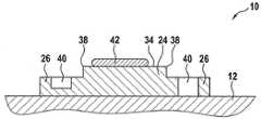
图1示出了包括衬底12的功率半导体模块10,功率半导体芯片14经由第一(底部)功率电极16结合到该衬底12。例如,功率半导体芯片14可以提供二极管、晶闸管和/或晶体管。电极16可以是源电极或发射电极。功率半导体芯片14可以基于Si或SiC。FIG. 1 shows a
衬底12可以具有(顶侧)金属化层18,功率半导体芯片14结合到该金属化层18,并且衬底12可以在相反侧具有(底侧)金属化层20。利用金属化层20,衬底12可以结合到功率半导体模块10的基板22。金属化层18可以被构造成提供功率半导体芯片14到功率半导体模块10的其他部件的电连接。金属化层18、20可以由Cu制成。The
金属板24结合到功率半导体芯片14的顶侧,该金属板可以由Cu或Mo制成。在与结合到金属化层18的一侧相反的一侧上,功率半导体芯片14具有另外的(顶部)功率电极26,金属板24接合到该功率电极26。还可以的是,功率半导体芯片14在与功率电极26相同的一侧具有栅电极28。电极16、26和28可以由Cu制成。电极26和可选地电极28可以比金属板24薄例如至少五倍。Bonded to the top side of the
栅电极可以利用引线结合件30连接到金属化层18的一部分。而且,金属板24以及因此功率电极26可以利用一个或多个另外的引线结合件32连接到金属化层18的一部分,该一个或多个另外的引线结合件32的直径可以比引线结合件30更大。The gate electrode may be connected to a portion of
一个或多个另外的引线结合件32被结合到金属板24的中央部分34。One or more
金属板24构造成使得与中央部分34相比,在边界36处(即,在中央部分34的外侧)具有更少的每单位面积金属材料。在边界处,金属板24具有减少的金属材料。在图1所示的情况下,在与金属板24沿着功率半导体芯片14的延伸方向正交的方向上,边界36比中央部分34更薄。The
利用这样的边界36(即,具有减少的金属材料的边界36),可以减小由热循环引起的应力。With such a boundary 36 (ie, a
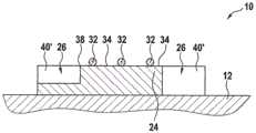
图2示出了具有含有减少的金属材料的边界36的功率半导体模块10的另外的实施例。类似于图1,边界36比中央部分34更薄。边界36具有总体恒定的厚度。如所示的,中央部分34也可以具有恒定的总体厚度。可以在边界36与中央部分34之间设置周缘38。FIG. 2 shows a further embodiment of a
然而,还可以的是,具有减小的厚度的边界36是倾斜的和/或具有变化的厚度。However, it is also possible that the
图2还示出了边界36完全围绕中央部分34。另外,边界36的宽度在金属板24的所有侧上可以是相同的。FIG. 2 also shows that the
图3示出了边界36的厚度可以与中央部分34相同,但是通过为边界设置凹坑和/或孔40而使金属板24的金属材料在边界36处减少。凹坑和/或孔40可以成一行或多行围绕中央部分34。FIG. 3 shows that the thickness of the
图4示出了凹坑和/或孔40可以仅部分地穿透边界36的厚度或者可以完全穿透边界36的厚度,即,可以是通孔。附加地,如图4所示,减小的边界厚度可以与凹坑和/或孔40进行组合。4 shows that the dimples and/or holes 40 may only partially penetrate the thickness of the
图4还示出了金属带42可以结合到中央部分34。必须注意的是,这样的金属带42也可以代替引线结合件32或附加于引线结合件32而被用于图1至图6所示的其他实施例中。FIG. 4 also shows that the
在图5中,示出了其他类型的凹陷40',其可以仅部分地穿透边界36的厚度或者可以完全穿透边界36的厚度。再一次,边界36的厚度与中央部分34的厚度相比可以相等或更小。In FIG. 5 , other types of
如图6所示,凹陷40'可以围绕中央部分34成行设置,该行可以完全围绕中央部分。与孔40相反,凹陷40'可以延伸到金属板24的边缘。As shown in FIG. 6, the recesses 40' may be arranged in a row around the
图7示出了用于制造如图1至图6所示的功率半导体模块10的方法的流程图。FIG. 7 shows a flowchart of a method for manufacturing the
在步骤S10中,功率半导体芯片14以其功率电极16结合到衬底12的金属化层18。该结合可以通过焊接或烧结来执行。可以使用与关于步骤S14所描述的相同的烧结过程。In step S10 , the
在步骤S12中,金属板24的边界36被构造成使得与金属板24的中央部分34相比,金属板24在边界36处具有更少的每单位面积金属材料。In step S12 , the
可以利用电化学蚀刻来构造金属板24的边界36。如图1至图4所示,可以利用电化学蚀刻来产生不同厚度的边界36。如图3至图6所示,可以利用电化学蚀刻来产生凹陷40'和/或孔40。The
附加地或替换地,通过冲压来构造金属板24的边界36。如关于图3至图6所示,可以利用电化学蚀刻来产生凹陷40'和/或孔40。Additionally or alternatively, the
在步骤S14中,将金属板24与衬底12相反地结合到功率半导体芯片14。In step S14 , the
金属板24被烧结到功率半导体芯片14。例如,金属板24可以利用例如由Ag或Cu制成的纳米颗粒烧结到功率半导体芯片14。The
在步骤S16中,互连元件32、42中的一个或多个被结合到金属板24的中央部分34。In step S16 one or more of the interconnecting
例如,互连元件32、42(诸如引线结合件32)可以被超声焊接到中央部分34。还可以的是,诸如金属带42之类的互连元件32、42被激光焊接到中央部分34。For example,
虽然已经在附图和前面的描述中图示和描述了本发明,但是这样的图示和描述将被认为是说明性的或示例性的而非限制性的;本发明不限于所公开的实施例。根据对附图、公开内容和所附权利要求的研究,对所公开实施例的其他变化可以被本领域中的并且实践所要求保护的发明的技术人员理解和实现。在权利要求中,词语“包括”不排除其他元件或步骤,并且不定冠词“一”或“一个”不排除多个。单个处理器或控制器或其他单元可以实现权利要求中所叙述的若干个项的功能。在相互不同的从属权利要求中记载了某些措施这一纯粹事实并不指示这些措施的组合不能被用来获利。权利要求中的任何附图标记不应被解释为限制范围。While the invention has been illustrated and described in the drawings and foregoing description, such illustration and description are to be considered illustrative or exemplary and not restrictive; the invention is not limited to the disclosed implementations example. Other variations to the disclosed embodiments may be understood and effected by those skilled in the art and practicing the claimed invention, from a study of the drawings, the disclosure, and the appended claims. In the claims, the word "comprising" does not exclude other elements or steps, and the indefinite article "a" or "an" does not exclude a plurality. A single processor or controller or other unit may fulfill the functions of several items recited in the claims. The mere fact that certain measures are recited in mutually different dependent claims does not indicate that a combination of these measures cannot be used to advantage. Any reference signs in the claims should not be construed as limiting the scope.
附图说明列表List of accompanying drawings
10 功率半导体模块10 Power semiconductor modules
12 衬底12 Substrate
14 功率半导体芯片14 Power semiconductor chips
16 功率电极16 Power electrodes
18 金属化层18 Metallization
20 金属化层20 Metallization
22 基板22 substrate
24 金属板24 sheet metal
26 功率电极26 Power electrodes
28 栅电极28 Gate electrode
30 引线结合件30 Wire Bonds
32 引线结合件32 Wire Bonds
34 中央部分34 Central Section
36 边界36 borders
38 周缘38 perimeter
40 孔40 holes
40' 凹陷40' recess
42 金属带42 metal belt
Claims (15)
Applications Claiming Priority (3)
| Application Number | Priority Date | Filing Date | Title |
|---|---|---|---|
| EP18166775 | 2018-04-11 | ||
| EP18166775.9 | 2018-04-11 | ||
| PCT/EP2019/058748WO2019197304A1 (en) | 2018-04-11 | 2019-04-08 | Material reduced metallic plate on power semiconductor chip |
Publications (2)
| Publication Number | Publication Date |
|---|---|
| CN111937127Atrue CN111937127A (en) | 2020-11-13 |
| CN111937127B CN111937127B (en) | 2024-04-02 |
Family
ID=61971937
Family Applications (1)
| Application Number | Title | Priority Date | Filing Date |
|---|---|---|---|
| CN201980024501.4AActiveCN111937127B (en) | 2018-04-11 | 2019-04-08 | Material-reduced metal plates on power semiconductor chips |
Country Status (5)
| Country | Link |
|---|---|
| US (1) | US11538734B2 (en) |
| EP (1) | EP3776638A1 (en) |
| JP (1) | JP7437582B2 (en) |
| CN (1) | CN111937127B (en) |
| WO (1) | WO2019197304A1 (en) |
Families Citing this family (3)
| Publication number | Priority date | Publication date | Assignee | Title |
|---|---|---|---|---|
| DE102019108932B4 (en)* | 2019-04-05 | 2022-04-21 | Danfoss Silicon Power Gmbh | Semiconductor module and method for its manufacture |
| EP3872848A1 (en)* | 2020-02-27 | 2021-09-01 | Littelfuse, Inc. | Metal tab for chip assembly |
| WO2021176996A1 (en)* | 2020-03-04 | 2021-09-10 | ローム株式会社 | Semiconductor device and method for manufacturing semiconductor device |
Citations (6)
| Publication number | Priority date | Publication date | Assignee | Title |
|---|---|---|---|---|
| JPH01122129A (en)* | 1987-11-05 | 1989-05-15 | Sumitomo Electric Ind Ltd | Wire connection pad |
| JP2000307043A (en)* | 1999-04-22 | 2000-11-02 | Mitsubishi Electric Corp | Power semiconductor module |
| CN102054830A (en)* | 2009-09-30 | 2011-05-11 | 英飞凌科技股份有限公司 | Power semiconductor module and method for driving the same |
| US20140306328A1 (en)* | 2013-04-16 | 2014-10-16 | Rohm Co., Ltd. | Semiconductor device |
| WO2016143557A1 (en)* | 2015-03-10 | 2016-09-15 | 三菱電機株式会社 | Power semiconductor device |
| JP2017005037A (en)* | 2015-06-08 | 2017-01-05 | 三菱電機株式会社 | Power semiconductor device |
Family Cites Families (17)
| Publication number | Priority date | Publication date | Assignee | Title |
|---|---|---|---|---|
| EP0520294B1 (en) | 1991-06-24 | 1998-08-26 | Siemens Aktiengesellschaft | Semiconductor device and method of manufacturing the same |
| JP4309368B2 (en)* | 2005-03-30 | 2009-08-05 | エルピーダメモリ株式会社 | Semiconductor memory device |
| US7443014B2 (en)* | 2005-10-25 | 2008-10-28 | Infineon Technologies Ag | Electronic module and method of assembling the same |
| US8004075B2 (en)* | 2006-04-25 | 2011-08-23 | Hitachi, Ltd. | Semiconductor power module including epoxy resin coating |
| US8643172B2 (en)* | 2007-06-08 | 2014-02-04 | Freescale Semiconductor, Inc. | Heat spreader for center gate molding |
| US20090261462A1 (en)* | 2008-04-16 | 2009-10-22 | Jocel Gomez | Semiconductor package with stacked die assembly |
| US20110049580A1 (en)* | 2009-08-28 | 2011-03-03 | Sik Lui | Hybrid Packaged Gate Controlled Semiconductor Switching Device Using GaN MESFET |
| JP5542567B2 (en) | 2010-07-27 | 2014-07-09 | 三菱電機株式会社 | Semiconductor device |
| MY166609A (en)* | 2010-09-15 | 2018-07-17 | Semiconductor Components Ind Llc | Connector assembly and method of manufacture |
| US8680627B2 (en)* | 2011-01-14 | 2014-03-25 | International Rectifier Corporation | Stacked half-bridge package with a common conductive clip |
| US8299588B1 (en)* | 2011-07-07 | 2012-10-30 | Texas Instruments Incorporated | Structure and method for uniform current distribution in power supply module |
| US8643176B2 (en)* | 2011-07-27 | 2014-02-04 | Infineon Technologies Ag | Power semiconductor chip having two metal layers on one face |
| KR101977994B1 (en)* | 2013-06-28 | 2019-08-29 | 매그나칩 반도체 유한회사 | Semiconductor pacakge |
| US9385070B2 (en)* | 2013-06-28 | 2016-07-05 | Delta Electronics, Inc. | Semiconductor component having a lateral semiconductor device and a vertical semiconductor device |
| DE102014008587B4 (en) | 2014-06-10 | 2022-01-05 | Vitesco Technologies GmbH | Power semiconductor circuit |
| DE102014222819B4 (en) | 2014-11-07 | 2019-01-03 | Danfoss Silicon Power Gmbh | Power semiconductor contact structure with bonding buffer and method for its production |
| WO2017157486A1 (en) | 2016-03-16 | 2017-09-21 | Abb Schweiz Ag | Semiconductor device |
- 2019
- 2019-04-08EPEP19714683.0Apatent/EP3776638A1/enactivePending
- 2019-04-08WOPCT/EP2019/058748patent/WO2019197304A1/ennot_activeCeased
- 2019-04-08JPJP2020555462Apatent/JP7437582B2/enactiveActive
- 2019-04-08CNCN201980024501.4Apatent/CN111937127B/enactiveActive
- 2019-04-08USUS17/046,620patent/US11538734B2/enactiveActive
Patent Citations (6)
| Publication number | Priority date | Publication date | Assignee | Title |
|---|---|---|---|---|
| JPH01122129A (en)* | 1987-11-05 | 1989-05-15 | Sumitomo Electric Ind Ltd | Wire connection pad |
| JP2000307043A (en)* | 1999-04-22 | 2000-11-02 | Mitsubishi Electric Corp | Power semiconductor module |
| CN102054830A (en)* | 2009-09-30 | 2011-05-11 | 英飞凌科技股份有限公司 | Power semiconductor module and method for driving the same |
| US20140306328A1 (en)* | 2013-04-16 | 2014-10-16 | Rohm Co., Ltd. | Semiconductor device |
| WO2016143557A1 (en)* | 2015-03-10 | 2016-09-15 | 三菱電機株式会社 | Power semiconductor device |
| JP2017005037A (en)* | 2015-06-08 | 2017-01-05 | 三菱電機株式会社 | Power semiconductor device |
Also Published As
| Publication number | Publication date |
|---|---|
| JP2021521641A (en) | 2021-08-26 |
| US11538734B2 (en) | 2022-12-27 |
| WO2019197304A1 (en) | 2019-10-17 |
| EP3776638A1 (en) | 2021-02-17 |
| JP7437582B2 (en) | 2024-02-26 |
| US20210104449A1 (en) | 2021-04-08 |
| CN111937127B (en) | 2024-04-02 |
Similar Documents
| Publication | Publication Date | Title |
|---|---|---|
| CN110622301B (en) | Power semiconductor device and method for manufacturing the same | |
| JP5983889B2 (en) | Manufacturing method of semiconductor device | |
| JP6152842B2 (en) | Semiconductor device and manufacturing method thereof | |
| CN107210241A (en) | Power semiconductor arrangement | |
| JP6726112B2 (en) | Semiconductor device and power converter | |
| CN104821282A (en) | Power semiconductor module | |
| CN111937127B (en) | Material-reduced metal plates on power semiconductor chips | |
| JP6868455B2 (en) | Electronic component package and its manufacturing method | |
| CN104064529B (en) | The method of semiconductor devices, semiconductor module and manufacture semiconductor devices and semiconductor module | |
| TW200947656A (en) | Lead frame, electronic component with the same, and manufacturing method thereof | |
| KR102228945B1 (en) | Semiconductor package and method of fabricating the same | |
| CN109075159B (en) | Semiconductor device and method for manufacturing the same | |
| CN115020258A (en) | Semiconductor device, power module, method for manufacturing semiconductor device, and semiconductor module | |
| JP6860334B2 (en) | Semiconductor device | |
| JP6317178B2 (en) | Circuit board and electronic device | |
| CN119965171A (en) | Stacked semiconductor module with double-sided heat dissipation structure and manufacturing method thereof | |
| US20220344552A1 (en) | Light-emitting device and manufacturing method of the same | |
| JP2016086003A (en) | Method for manufacturing power semiconductor device | |
| JP6299568B2 (en) | Semiconductor device | |
| CN115000023A (en) | Substrate having solder stop structure, method for manufacturing the same, and electronic device | |
| JP5418654B2 (en) | Semiconductor device | |
| JP6558969B2 (en) | Semiconductor chip, semiconductor device and manufacturing method thereof | |
| JP7492375B2 (en) | Semiconductor Device | |
| US20240170373A1 (en) | Semiconductor device | |
| JP7656152B2 (en) | Semiconductor Device |
Legal Events
| Date | Code | Title | Description |
|---|---|---|---|
| PB01 | Publication | ||
| PB01 | Publication | ||
| SE01 | Entry into force of request for substantive examination | ||
| SE01 | Entry into force of request for substantive examination | ||
| CB02 | Change of applicant information | Address after:Swiss Baden Applicant after:Hitachi energy Switzerland AG Address before:Swiss Baden Applicant before:ABB grid Switzerland AG | |
| CB02 | Change of applicant information | ||
| TA01 | Transfer of patent application right | Effective date of registration:20240117 Address after:Zurich, SUI Applicant after:Hitachi Energy Co.,Ltd. Address before:Swiss Baden Applicant before:Hitachi energy Switzerland AG | |
| TA01 | Transfer of patent application right | ||
| GR01 | Patent grant | ||
| GR01 | Patent grant |