CN111936902B - Fabrication of metal optical metasurfaces - Google Patents
Fabrication of metal optical metasurfacesDownload PDFInfo
- Publication number
- CN111936902B CN111936902BCN201980024530.0ACN201980024530ACN111936902BCN 111936902 BCN111936902 BCN 111936902BCN 201980024530 ACN201980024530 ACN 201980024530ACN 111936902 BCN111936902 BCN 111936902B
- Authority
- CN
- China
- Prior art keywords
- copper
- dielectric
- layer
- backplane structure
- barrier layer
- Prior art date
- Legal status (The legal status is an assumption and is not a legal conclusion. Google has not performed a legal analysis and makes no representation as to the accuracy of the status listed.)
- Active
Links
- 230000003287optical effectEffects0.000titleclaimsabstractdescription42
- 229910052751metalInorganic materials0.000titleclaimsdescription86
- 239000002184metalSubstances0.000titleclaimsdescription86
- 238000004519manufacturing processMethods0.000titleclaimsdescription12
- 239000010949copperSubstances0.000claimsabstractdescription250
- RYGMFSIKBFXOCR-UHFFFAOYSA-NCopperChemical compound[Cu]RYGMFSIKBFXOCR-UHFFFAOYSA-N0.000claimsabstractdescription249
- 229910052802copperInorganic materials0.000claimsabstractdescription249
- 238000000034methodMethods0.000claimsabstractdescription128
- 230000004888barrier functionEffects0.000claimsabstractdescription86
- 230000008569processEffects0.000claimsabstractdescription45
- 239000003989dielectric materialSubstances0.000claimsabstractdescription40
- 239000011248coating agentSubstances0.000claimsabstractdescription29
- 238000000576coating methodMethods0.000claimsabstractdescription29
- 238000000151depositionMethods0.000claimsabstractdescription21
- 239000000463materialSubstances0.000claimsdescription56
- 125000006850spacer groupChemical group0.000claimsdescription18
- 239000000758substrateSubstances0.000claimsdescription16
- 239000012780transparent materialSubstances0.000claimsdescription15
- 238000005530etchingMethods0.000claimsdescription13
- 238000009792diffusion processMethods0.000claimsdescription12
- 229910004298SiO 2Inorganic materials0.000claimsdescription10
- 239000011521glassSubstances0.000claimsdescription10
- 230000036961partial effectEffects0.000claimsdescription10
- 229920000642polymerPolymers0.000claimsdescription9
- 239000000126substanceSubstances0.000claimsdescription8
- 238000005260corrosionMethods0.000claimsdescription5
- 230000007797corrosionEffects0.000claimsdescription5
- 229910052715tantalumInorganic materials0.000claimsdescription5
- 239000004973liquid crystal related substanceSubstances0.000claimsdescription4
- 238000004544sputter depositionMethods0.000claimsdescription4
- MZLGASXMSKOWSE-UHFFFAOYSA-Ntantalum nitrideChemical compound[Ta]#NMZLGASXMSKOWSE-UHFFFAOYSA-N0.000claimsdescription4
- 239000005387chalcogenide glassSubstances0.000claimsdescription3
- 238000009713electroplatingMethods0.000claimsdescription3
- 239000002861polymer materialSubstances0.000claimsdescription3
- 238000005498polishingMethods0.000claimsdescription2
- GUVRBAGPIYLISA-UHFFFAOYSA-Ntantalum atomChemical compound[Ta]GUVRBAGPIYLISA-UHFFFAOYSA-N0.000claims2
- 239000010410layerSubstances0.000description191
- 230000009977dual effectEffects0.000description9
- 150000004767nitridesChemical class0.000description7
- 229910052581Si3N4Inorganic materials0.000description6
- 239000004020conductorSubstances0.000description6
- 239000011162core materialSubstances0.000description6
- 238000013461designMethods0.000description6
- 239000004065semiconductorSubstances0.000description6
- HQVNEWCFYHHQES-UHFFFAOYSA-Nsilicon nitrideChemical compoundN12[Si]34N5[Si]62N3[Si]51N64HQVNEWCFYHHQES-UHFFFAOYSA-N0.000description6
- VYPSYNLAJGMNEJ-UHFFFAOYSA-NSilicium dioxideChemical compoundO=[Si]=OVYPSYNLAJGMNEJ-UHFFFAOYSA-N0.000description5
- 229910052782aluminiumInorganic materials0.000description5
- XAGFODPZIPBFFR-UHFFFAOYSA-NaluminiumChemical compound[Al]XAGFODPZIPBFFR-UHFFFAOYSA-N0.000description5
- 238000003486chemical etchingMethods0.000description5
- 239000012212insulatorSubstances0.000description5
- 238000005240physical vapour depositionMethods0.000description5
- 238000000623plasma-assisted chemical vapour depositionMethods0.000description5
- 229910052814silicon oxideInorganic materials0.000description5
- 229910018072Al 2 O 3Inorganic materials0.000description4
- -1SiCNChemical compound0.000description4
- 230000008901benefitEffects0.000description4
- 238000001020plasma etchingMethods0.000description4
- HBMJWWWQQXIZIP-UHFFFAOYSA-Nsilicon carbideChemical compound[Si+]#[C-]HBMJWWWQQXIZIP-UHFFFAOYSA-N0.000description4
- 238000005229chemical vapour depositionMethods0.000description3
- 230000008878couplingEffects0.000description3
- 238000010168coupling processMethods0.000description3
- 238000005859coupling reactionMethods0.000description3
- 238000005516engineering processMethods0.000description3
- 229910004140HfOInorganic materials0.000description2
- XUIMIQQOPSSXEZ-UHFFFAOYSA-NSiliconChemical compound[Si]XUIMIQQOPSSXEZ-UHFFFAOYSA-N0.000description2
- 101150044878US18 geneProteins0.000description2
- HMDDXIMCDZRSNE-UHFFFAOYSA-N[C].[Si]Chemical compound[C].[Si]HMDDXIMCDZRSNE-UHFFFAOYSA-N0.000description2
- 229910021417amorphous siliconInorganic materials0.000description2
- 238000000231atomic layer depositionMethods0.000description2
- 230000008021depositionEffects0.000description2
- 238000001312dry etchingMethods0.000description2
- CJNBYAVZURUTKZ-UHFFFAOYSA-Nhafnium(iv) oxideChemical compoundO=[Hf]=OCJNBYAVZURUTKZ-UHFFFAOYSA-N0.000description2
- 230000031700light absorptionEffects0.000description2
- 238000001465metallisationMethods0.000description2
- TWNQGVIAIRXVLR-UHFFFAOYSA-Noxo(oxoalumanyloxy)alumaneChemical compoundO=[Al]O[Al]=OTWNQGVIAIRXVLR-UHFFFAOYSA-N0.000description2
- 238000000059patterningMethods0.000description2
- 229920003229poly(methyl methacrylate)Polymers0.000description2
- 239000004926polymethyl methacrylateSubstances0.000description2
- 239000011241protective layerSubstances0.000description2
- 230000002829reductive effectEffects0.000description2
- 230000035945sensitivityEffects0.000description2
- 229910052710siliconInorganic materials0.000description2
- 239000010703siliconSubstances0.000description2
- 229910010271silicon carbideInorganic materials0.000description2
- BQCADISMDOOEFD-UHFFFAOYSA-NSilverChemical compound[Ag]BQCADISMDOOEFD-UHFFFAOYSA-N0.000description1
- 238000003491arrayMethods0.000description1
- 230000000903blocking effectEffects0.000description1
- 238000010276constructionMethods0.000description1
- 229910021419crystalline siliconInorganic materials0.000description1
- 238000013016dampingMethods0.000description1
- 230000005516deep trapEffects0.000description1
- 238000001514detection methodMethods0.000description1
- 238000011161developmentMethods0.000description1
- 230000000694effectsEffects0.000description1
- 230000005684electric fieldEffects0.000description1
- 238000004070electrodepositionMethods0.000description1
- 230000005686electrostatic fieldEffects0.000description1
- 238000005538encapsulationMethods0.000description1
- PCHJSUWPFVWCPO-UHFFFAOYSA-NgoldChemical compound[Au]PCHJSUWPFVWCPO-UHFFFAOYSA-N0.000description1
- 229910052737goldInorganic materials0.000description1
- 239000010931goldSubstances0.000description1
- 230000036039immunityEffects0.000description1
- 230000010354integrationEffects0.000description1
- 230000000670limiting effectEffects0.000description1
- 238000013507mappingMethods0.000description1
- 230000000873masking effectEffects0.000description1
- 150000002739metalsChemical class0.000description1
- 230000005012migrationEffects0.000description1
- 238000013508migrationMethods0.000description1
- 238000012986modificationMethods0.000description1
- 230000004048modificationEffects0.000description1
- 238000002161passivationMethods0.000description1
- 238000009304pastoral farmingMethods0.000description1
- 229920002120photoresistant polymerPolymers0.000description1
- 239000004417polycarbonateSubstances0.000description1
- 229920000515polycarbonatePolymers0.000description1
- LIVNPJMFVYWSIS-UHFFFAOYSA-Nsilicon monoxideChemical compound[Si-]#[O+]LIVNPJMFVYWSIS-UHFFFAOYSA-N0.000description1
- 229910052709silverInorganic materials0.000description1
- 239000004332silverSubstances0.000description1
- 239000007787solidSubstances0.000description1
- 230000003068static effectEffects0.000description1
Images


Classifications
- C—CHEMISTRY; METALLURGY
- C23—COATING METALLIC MATERIAL; COATING MATERIAL WITH METALLIC MATERIAL; CHEMICAL SURFACE TREATMENT; DIFFUSION TREATMENT OF METALLIC MATERIAL; COATING BY VACUUM EVAPORATION, BY SPUTTERING, BY ION IMPLANTATION OR BY CHEMICAL VAPOUR DEPOSITION, IN GENERAL; INHIBITING CORROSION OF METALLIC MATERIAL OR INCRUSTATION IN GENERAL
- C23C—COATING METALLIC MATERIAL; COATING MATERIAL WITH METALLIC MATERIAL; SURFACE TREATMENT OF METALLIC MATERIAL BY DIFFUSION INTO THE SURFACE, BY CHEMICAL CONVERSION OR SUBSTITUTION; COATING BY VACUUM EVAPORATION, BY SPUTTERING, BY ION IMPLANTATION OR BY CHEMICAL VAPOUR DEPOSITION, IN GENERAL
- C23C28/00—Coating for obtaining at least two superposed coatings either by methods not provided for in a single one of groups C23C2/00 - C23C26/00 or by combinations of methods provided for in subclasses C23C and C25C or C25D
- C23C28/30—Coatings combining at least one metallic layer and at least one inorganic non-metallic layer
- C23C28/32—Coatings combining at least one metallic layer and at least one inorganic non-metallic layer including at least one pure metallic layer
- C23C28/322—Coatings combining at least one metallic layer and at least one inorganic non-metallic layer including at least one pure metallic layer only coatings of metal elements only
- G—PHYSICS
- G02—OPTICS
- G02B—OPTICAL ELEMENTS, SYSTEMS OR APPARATUS
- G02B5/00—Optical elements other than lenses
- G02B5/32—Holograms used as optical elements
- C—CHEMISTRY; METALLURGY
- C23—COATING METALLIC MATERIAL; COATING MATERIAL WITH METALLIC MATERIAL; CHEMICAL SURFACE TREATMENT; DIFFUSION TREATMENT OF METALLIC MATERIAL; COATING BY VACUUM EVAPORATION, BY SPUTTERING, BY ION IMPLANTATION OR BY CHEMICAL VAPOUR DEPOSITION, IN GENERAL; INHIBITING CORROSION OF METALLIC MATERIAL OR INCRUSTATION IN GENERAL
- C23C—COATING METALLIC MATERIAL; COATING MATERIAL WITH METALLIC MATERIAL; SURFACE TREATMENT OF METALLIC MATERIAL BY DIFFUSION INTO THE SURFACE, BY CHEMICAL CONVERSION OR SUBSTITUTION; COATING BY VACUUM EVAPORATION, BY SPUTTERING, BY ION IMPLANTATION OR BY CHEMICAL VAPOUR DEPOSITION, IN GENERAL
- C23C14/00—Coating by vacuum evaporation, by sputtering or by ion implantation of the coating forming material
- C23C14/02—Pretreatment of the material to be coated
- C23C14/021—Cleaning or etching treatments
- C—CHEMISTRY; METALLURGY
- C23—COATING METALLIC MATERIAL; COATING MATERIAL WITH METALLIC MATERIAL; CHEMICAL SURFACE TREATMENT; DIFFUSION TREATMENT OF METALLIC MATERIAL; COATING BY VACUUM EVAPORATION, BY SPUTTERING, BY ION IMPLANTATION OR BY CHEMICAL VAPOUR DEPOSITION, IN GENERAL; INHIBITING CORROSION OF METALLIC MATERIAL OR INCRUSTATION IN GENERAL
- C23C—COATING METALLIC MATERIAL; COATING MATERIAL WITH METALLIC MATERIAL; SURFACE TREATMENT OF METALLIC MATERIAL BY DIFFUSION INTO THE SURFACE, BY CHEMICAL CONVERSION OR SUBSTITUTION; COATING BY VACUUM EVAPORATION, BY SPUTTERING, BY ION IMPLANTATION OR BY CHEMICAL VAPOUR DEPOSITION, IN GENERAL
- C23C14/00—Coating by vacuum evaporation, by sputtering or by ion implantation of the coating forming material
- C23C14/06—Coating by vacuum evaporation, by sputtering or by ion implantation of the coating forming material characterised by the coating material
- C23C14/14—Metallic material, boron or silicon
- C23C14/18—Metallic material, boron or silicon on other inorganic substrates
- C23C14/185—Metallic material, boron or silicon on other inorganic substrates by cathodic sputtering
- C—CHEMISTRY; METALLURGY
- C23—COATING METALLIC MATERIAL; COATING MATERIAL WITH METALLIC MATERIAL; CHEMICAL SURFACE TREATMENT; DIFFUSION TREATMENT OF METALLIC MATERIAL; COATING BY VACUUM EVAPORATION, BY SPUTTERING, BY ION IMPLANTATION OR BY CHEMICAL VAPOUR DEPOSITION, IN GENERAL; INHIBITING CORROSION OF METALLIC MATERIAL OR INCRUSTATION IN GENERAL
- C23C—COATING METALLIC MATERIAL; COATING MATERIAL WITH METALLIC MATERIAL; SURFACE TREATMENT OF METALLIC MATERIAL BY DIFFUSION INTO THE SURFACE, BY CHEMICAL CONVERSION OR SUBSTITUTION; COATING BY VACUUM EVAPORATION, BY SPUTTERING, BY ION IMPLANTATION OR BY CHEMICAL VAPOUR DEPOSITION, IN GENERAL
- C23C14/00—Coating by vacuum evaporation, by sputtering or by ion implantation of the coating forming material
- C23C14/22—Coating by vacuum evaporation, by sputtering or by ion implantation of the coating forming material characterised by the process of coating
- C23C14/34—Sputtering
- C—CHEMISTRY; METALLURGY
- C23—COATING METALLIC MATERIAL; COATING MATERIAL WITH METALLIC MATERIAL; CHEMICAL SURFACE TREATMENT; DIFFUSION TREATMENT OF METALLIC MATERIAL; COATING BY VACUUM EVAPORATION, BY SPUTTERING, BY ION IMPLANTATION OR BY CHEMICAL VAPOUR DEPOSITION, IN GENERAL; INHIBITING CORROSION OF METALLIC MATERIAL OR INCRUSTATION IN GENERAL
- C23C—COATING METALLIC MATERIAL; COATING MATERIAL WITH METALLIC MATERIAL; SURFACE TREATMENT OF METALLIC MATERIAL BY DIFFUSION INTO THE SURFACE, BY CHEMICAL CONVERSION OR SUBSTITUTION; COATING BY VACUUM EVAPORATION, BY SPUTTERING, BY ION IMPLANTATION OR BY CHEMICAL VAPOUR DEPOSITION, IN GENERAL
- C23C28/00—Coating for obtaining at least two superposed coatings either by methods not provided for in a single one of groups C23C2/00 - C23C26/00 or by combinations of methods provided for in subclasses C23C and C25C or C25D
- C23C28/30—Coatings combining at least one metallic layer and at least one inorganic non-metallic layer
- C23C28/34—Coatings combining at least one metallic layer and at least one inorganic non-metallic layer including at least one inorganic non-metallic material layer, e.g. metal carbide, nitride, boride, silicide layer and their mixtures, enamels, phosphates and sulphates
- C23C28/341—Coatings combining at least one metallic layer and at least one inorganic non-metallic layer including at least one inorganic non-metallic material layer, e.g. metal carbide, nitride, boride, silicide layer and their mixtures, enamels, phosphates and sulphates with at least one carbide layer
- C—CHEMISTRY; METALLURGY
- C23—COATING METALLIC MATERIAL; COATING MATERIAL WITH METALLIC MATERIAL; CHEMICAL SURFACE TREATMENT; DIFFUSION TREATMENT OF METALLIC MATERIAL; COATING BY VACUUM EVAPORATION, BY SPUTTERING, BY ION IMPLANTATION OR BY CHEMICAL VAPOUR DEPOSITION, IN GENERAL; INHIBITING CORROSION OF METALLIC MATERIAL OR INCRUSTATION IN GENERAL
- C23C—COATING METALLIC MATERIAL; COATING MATERIAL WITH METALLIC MATERIAL; SURFACE TREATMENT OF METALLIC MATERIAL BY DIFFUSION INTO THE SURFACE, BY CHEMICAL CONVERSION OR SUBSTITUTION; COATING BY VACUUM EVAPORATION, BY SPUTTERING, BY ION IMPLANTATION OR BY CHEMICAL VAPOUR DEPOSITION, IN GENERAL
- C23C28/00—Coating for obtaining at least two superposed coatings either by methods not provided for in a single one of groups C23C2/00 - C23C26/00 or by combinations of methods provided for in subclasses C23C and C25C or C25D
- C23C28/30—Coatings combining at least one metallic layer and at least one inorganic non-metallic layer
- C23C28/34—Coatings combining at least one metallic layer and at least one inorganic non-metallic layer including at least one inorganic non-metallic material layer, e.g. metal carbide, nitride, boride, silicide layer and their mixtures, enamels, phosphates and sulphates
- C23C28/345—Coatings combining at least one metallic layer and at least one inorganic non-metallic layer including at least one inorganic non-metallic material layer, e.g. metal carbide, nitride, boride, silicide layer and their mixtures, enamels, phosphates and sulphates with at least one oxide layer
- C23C28/3455—Coatings combining at least one metallic layer and at least one inorganic non-metallic layer including at least one inorganic non-metallic material layer, e.g. metal carbide, nitride, boride, silicide layer and their mixtures, enamels, phosphates and sulphates with at least one oxide layer with a refractory ceramic layer, e.g. refractory metal oxide, ZrO2, rare earth oxides or a thermal barrier system comprising at least one refractory oxide layer
- C—CHEMISTRY; METALLURGY
- C25—ELECTROLYTIC OR ELECTROPHORETIC PROCESSES; APPARATUS THEREFOR
- C25D—PROCESSES FOR THE ELECTROLYTIC OR ELECTROPHORETIC PRODUCTION OF COATINGS; ELECTROFORMING; APPARATUS THEREFOR
- C25D3/00—Electroplating: Baths therefor
- C25D3/02—Electroplating: Baths therefor from solutions
- C25D3/38—Electroplating: Baths therefor from solutions of copper
- C—CHEMISTRY; METALLURGY
- C25—ELECTROLYTIC OR ELECTROPHORETIC PROCESSES; APPARATUS THEREFOR
- C25D—PROCESSES FOR THE ELECTROLYTIC OR ELECTROPHORETIC PRODUCTION OF COATINGS; ELECTROFORMING; APPARATUS THEREFOR
- C25D5/00—Electroplating characterised by the process; Pretreatment or after-treatment of workpieces
- C25D5/02—Electroplating of selected surface areas
- C—CHEMISTRY; METALLURGY
- C25—ELECTROLYTIC OR ELECTROPHORETIC PROCESSES; APPARATUS THEREFOR
- C25D—PROCESSES FOR THE ELECTROLYTIC OR ELECTROPHORETIC PRODUCTION OF COATINGS; ELECTROFORMING; APPARATUS THEREFOR
- C25D5/00—Electroplating characterised by the process; Pretreatment or after-treatment of workpieces
- C25D5/34—Pretreatment of metallic surfaces to be electroplated
- C—CHEMISTRY; METALLURGY
- C25—ELECTROLYTIC OR ELECTROPHORETIC PROCESSES; APPARATUS THEREFOR
- C25D—PROCESSES FOR THE ELECTROLYTIC OR ELECTROPHORETIC PRODUCTION OF COATINGS; ELECTROFORMING; APPARATUS THEREFOR
- C25D5/00—Electroplating characterised by the process; Pretreatment or after-treatment of workpieces
- C25D5/48—After-treatment of electroplated surfaces
- C—CHEMISTRY; METALLURGY
- C25—ELECTROLYTIC OR ELECTROPHORETIC PROCESSES; APPARATUS THEREFOR
- C25D—PROCESSES FOR THE ELECTROLYTIC OR ELECTROPHORETIC PRODUCTION OF COATINGS; ELECTROFORMING; APPARATUS THEREFOR
- C25D7/00—Electroplating characterised by the article coated
- C25D7/12—Semiconductors
- C25D7/123—Semiconductors first coated with a seed layer or a conductive layer
- G—PHYSICS
- G02—OPTICS
- G02B—OPTICAL ELEMENTS, SYSTEMS OR APPARATUS
- G02B1/00—Optical elements characterised by the material of which they are made; Optical coatings for optical elements
- G02B1/002—Optical elements characterised by the material of which they are made; Optical coatings for optical elements made of materials engineered to provide properties not available in nature, e.g. metamaterials
- G—PHYSICS
- G02—OPTICS
- G02B—OPTICAL ELEMENTS, SYSTEMS OR APPARATUS
- G02B1/00—Optical elements characterised by the material of which they are made; Optical coatings for optical elements
- G02B1/04—Optical elements characterised by the material of which they are made; Optical coatings for optical elements made of organic materials, e.g. plastics
- G—PHYSICS
- G02—OPTICS
- G02F—OPTICAL DEVICES OR ARRANGEMENTS FOR THE CONTROL OF LIGHT BY MODIFICATION OF THE OPTICAL PROPERTIES OF THE MEDIA OF THE ELEMENTS INVOLVED THEREIN; NON-LINEAR OPTICS; FREQUENCY-CHANGING OF LIGHT; OPTICAL LOGIC ELEMENTS; OPTICAL ANALOGUE/DIGITAL CONVERTERS
- G02F1/00—Devices or arrangements for the control of the intensity, colour, phase, polarisation or direction of light arriving from an independent light source, e.g. switching, gating or modulating; Non-linear optics
- G02F1/01—Devices or arrangements for the control of the intensity, colour, phase, polarisation or direction of light arriving from an independent light source, e.g. switching, gating or modulating; Non-linear optics for the control of the intensity, phase, polarisation or colour
- G02F1/19—Devices or arrangements for the control of the intensity, colour, phase, polarisation or direction of light arriving from an independent light source, e.g. switching, gating or modulating; Non-linear optics for the control of the intensity, phase, polarisation or colour based on variable-reflection or variable-refraction elements not provided for in groups G02F1/015 - G02F1/169
- G—PHYSICS
- G02—OPTICS
- G02F—OPTICAL DEVICES OR ARRANGEMENTS FOR THE CONTROL OF LIGHT BY MODIFICATION OF THE OPTICAL PROPERTIES OF THE MEDIA OF THE ELEMENTS INVOLVED THEREIN; NON-LINEAR OPTICS; FREQUENCY-CHANGING OF LIGHT; OPTICAL LOGIC ELEMENTS; OPTICAL ANALOGUE/DIGITAL CONVERTERS
- G02F1/00—Devices or arrangements for the control of the intensity, colour, phase, polarisation or direction of light arriving from an independent light source, e.g. switching, gating or modulating; Non-linear optics
- G02F1/01—Devices or arrangements for the control of the intensity, colour, phase, polarisation or direction of light arriving from an independent light source, e.g. switching, gating or modulating; Non-linear optics for the control of the intensity, phase, polarisation or colour
- G02F1/21—Devices or arrangements for the control of the intensity, colour, phase, polarisation or direction of light arriving from an independent light source, e.g. switching, gating or modulating; Non-linear optics for the control of the intensity, phase, polarisation or colour by interference
- G02F1/216—Devices or arrangements for the control of the intensity, colour, phase, polarisation or direction of light arriving from an independent light source, e.g. switching, gating or modulating; Non-linear optics for the control of the intensity, phase, polarisation or colour by interference using liquid crystals, e.g. liquid crystal Fabry-Perot filters
- G—PHYSICS
- G02—OPTICS
- G02F—OPTICAL DEVICES OR ARRANGEMENTS FOR THE CONTROL OF LIGHT BY MODIFICATION OF THE OPTICAL PROPERTIES OF THE MEDIA OF THE ELEMENTS INVOLVED THEREIN; NON-LINEAR OPTICS; FREQUENCY-CHANGING OF LIGHT; OPTICAL LOGIC ELEMENTS; OPTICAL ANALOGUE/DIGITAL CONVERTERS
- G02F1/00—Devices or arrangements for the control of the intensity, colour, phase, polarisation or direction of light arriving from an independent light source, e.g. switching, gating or modulating; Non-linear optics
- G02F1/29—Devices or arrangements for the control of the intensity, colour, phase, polarisation or direction of light arriving from an independent light source, e.g. switching, gating or modulating; Non-linear optics for the control of the position or the direction of light beams, i.e. deflection
- G02F1/292—Devices or arrangements for the control of the intensity, colour, phase, polarisation or direction of light arriving from an independent light source, e.g. switching, gating or modulating; Non-linear optics for the control of the position or the direction of light beams, i.e. deflection by controlled diffraction or phased-array beam steering
- G—PHYSICS
- G03—PHOTOGRAPHY; CINEMATOGRAPHY; ANALOGOUS TECHNIQUES USING WAVES OTHER THAN OPTICAL WAVES; ELECTROGRAPHY; HOLOGRAPHY
- G03H—HOLOGRAPHIC PROCESSES OR APPARATUS
- G03H1/00—Holographic processes or apparatus using light, infrared or ultraviolet waves for obtaining holograms or for obtaining an image from them; Details peculiar thereto
- G03H1/02—Details of features involved during the holographic process; Replication of holograms without interference recording
- G—PHYSICS
- G03—PHOTOGRAPHY; CINEMATOGRAPHY; ANALOGOUS TECHNIQUES USING WAVES OTHER THAN OPTICAL WAVES; ELECTROGRAPHY; HOLOGRAPHY
- G03H—HOLOGRAPHIC PROCESSES OR APPARATUS
- G03H1/00—Holographic processes or apparatus using light, infrared or ultraviolet waves for obtaining holograms or for obtaining an image from them; Details peculiar thereto
- G03H1/22—Processes or apparatus for obtaining an optical image from holograms
- G03H1/2294—Addressing the hologram to an active spatial light modulator
- B—PERFORMING OPERATIONS; TRANSPORTING
- B82—NANOTECHNOLOGY
- B82Y—SPECIFIC USES OR APPLICATIONS OF NANOSTRUCTURES; MEASUREMENT OR ANALYSIS OF NANOSTRUCTURES; MANUFACTURE OR TREATMENT OF NANOSTRUCTURES
- B82Y40/00—Manufacture or treatment of nanostructures
- G—PHYSICS
- G02—OPTICS
- G02B—OPTICAL ELEMENTS, SYSTEMS OR APPARATUS
- G02B5/00—Optical elements other than lenses
- G02B5/20—Filters
- G02B5/203—Filters having holographic or diffractive elements
- G—PHYSICS
- G02—OPTICS
- G02F—OPTICAL DEVICES OR ARRANGEMENTS FOR THE CONTROL OF LIGHT BY MODIFICATION OF THE OPTICAL PROPERTIES OF THE MEDIA OF THE ELEMENTS INVOLVED THEREIN; NON-LINEAR OPTICS; FREQUENCY-CHANGING OF LIGHT; OPTICAL LOGIC ELEMENTS; OPTICAL ANALOGUE/DIGITAL CONVERTERS
- G02F2201/00—Constructional arrangements not provided for in groups G02F1/00 - G02F7/00
- G02F2201/12—Constructional arrangements not provided for in groups G02F1/00 - G02F7/00 electrode
- G02F2201/122—Constructional arrangements not provided for in groups G02F1/00 - G02F7/00 electrode having a particular pattern
- G—PHYSICS
- G02—OPTICS
- G02F—OPTICAL DEVICES OR ARRANGEMENTS FOR THE CONTROL OF LIGHT BY MODIFICATION OF THE OPTICAL PROPERTIES OF THE MEDIA OF THE ELEMENTS INVOLVED THEREIN; NON-LINEAR OPTICS; FREQUENCY-CHANGING OF LIGHT; OPTICAL LOGIC ELEMENTS; OPTICAL ANALOGUE/DIGITAL CONVERTERS
- G02F2201/00—Constructional arrangements not provided for in groups G02F1/00 - G02F7/00
- G02F2201/30—Constructional arrangements not provided for in groups G02F1/00 - G02F7/00 grating
- G02F2201/307—Reflective grating, i.e. Bragg grating
- G—PHYSICS
- G02—OPTICS
- G02F—OPTICAL DEVICES OR ARRANGEMENTS FOR THE CONTROL OF LIGHT BY MODIFICATION OF THE OPTICAL PROPERTIES OF THE MEDIA OF THE ELEMENTS INVOLVED THEREIN; NON-LINEAR OPTICS; FREQUENCY-CHANGING OF LIGHT; OPTICAL LOGIC ELEMENTS; OPTICAL ANALOGUE/DIGITAL CONVERTERS
- G02F2201/00—Constructional arrangements not provided for in groups G02F1/00 - G02F7/00
- G02F2201/34—Constructional arrangements not provided for in groups G02F1/00 - G02F7/00 reflector
- G—PHYSICS
- G02—OPTICS
- G02F—OPTICAL DEVICES OR ARRANGEMENTS FOR THE CONTROL OF LIGHT BY MODIFICATION OF THE OPTICAL PROPERTIES OF THE MEDIA OF THE ELEMENTS INVOLVED THEREIN; NON-LINEAR OPTICS; FREQUENCY-CHANGING OF LIGHT; OPTICAL LOGIC ELEMENTS; OPTICAL ANALOGUE/DIGITAL CONVERTERS
- G02F2202/00—Materials and properties
- G02F2202/30—Metamaterials
- G—PHYSICS
- G02—OPTICS
- G02F—OPTICAL DEVICES OR ARRANGEMENTS FOR THE CONTROL OF LIGHT BY MODIFICATION OF THE OPTICAL PROPERTIES OF THE MEDIA OF THE ELEMENTS INVOLVED THEREIN; NON-LINEAR OPTICS; FREQUENCY-CHANGING OF LIGHT; OPTICAL LOGIC ELEMENTS; OPTICAL ANALOGUE/DIGITAL CONVERTERS
- G02F2202/00—Materials and properties
- G02F2202/36—Micro- or nanomaterials
- G—PHYSICS
- G02—OPTICS
- G02F—OPTICAL DEVICES OR ARRANGEMENTS FOR THE CONTROL OF LIGHT BY MODIFICATION OF THE OPTICAL PROPERTIES OF THE MEDIA OF THE ELEMENTS INVOLVED THEREIN; NON-LINEAR OPTICS; FREQUENCY-CHANGING OF LIGHT; OPTICAL LOGIC ELEMENTS; OPTICAL ANALOGUE/DIGITAL CONVERTERS
- G02F2203/00—Function characteristic
- G02F2203/10—Function characteristic plasmon
- G—PHYSICS
- G02—OPTICS
- G02F—OPTICAL DEVICES OR ARRANGEMENTS FOR THE CONTROL OF LIGHT BY MODIFICATION OF THE OPTICAL PROPERTIES OF THE MEDIA OF THE ELEMENTS INVOLVED THEREIN; NON-LINEAR OPTICS; FREQUENCY-CHANGING OF LIGHT; OPTICAL LOGIC ELEMENTS; OPTICAL ANALOGUE/DIGITAL CONVERTERS
- G02F2203/00—Function characteristic
- G02F2203/15—Function characteristic involving resonance effects, e.g. resonantly enhanced interaction
- G—PHYSICS
- G02—OPTICS
- G02F—OPTICAL DEVICES OR ARRANGEMENTS FOR THE CONTROL OF LIGHT BY MODIFICATION OF THE OPTICAL PROPERTIES OF THE MEDIA OF THE ELEMENTS INVOLVED THEREIN; NON-LINEAR OPTICS; FREQUENCY-CHANGING OF LIGHT; OPTICAL LOGIC ELEMENTS; OPTICAL ANALOGUE/DIGITAL CONVERTERS
- G02F2203/00—Function characteristic
- G02F2203/24—Function characteristic beam steering
- G—PHYSICS
- G02—OPTICS
- G02F—OPTICAL DEVICES OR ARRANGEMENTS FOR THE CONTROL OF LIGHT BY MODIFICATION OF THE OPTICAL PROPERTIES OF THE MEDIA OF THE ELEMENTS INVOLVED THEREIN; NON-LINEAR OPTICS; FREQUENCY-CHANGING OF LIGHT; OPTICAL LOGIC ELEMENTS; OPTICAL ANALOGUE/DIGITAL CONVERTERS
- G02F2203/00—Function characteristic
- G02F2203/50—Phase-only modulation
- G—PHYSICS
- G03—PHOTOGRAPHY; CINEMATOGRAPHY; ANALOGOUS TECHNIQUES USING WAVES OTHER THAN OPTICAL WAVES; ELECTROGRAPHY; HOLOGRAPHY
- G03H—HOLOGRAPHIC PROCESSES OR APPARATUS
- G03H2225/00—Active addressable light modulator
- G03H2225/20—Nature, e.g. e-beam addressed
- G03H2225/22—Electrically addressed SLM [EA-SLM]
- G—PHYSICS
- G03—PHOTOGRAPHY; CINEMATOGRAPHY; ANALOGOUS TECHNIQUES USING WAVES OTHER THAN OPTICAL WAVES; ELECTROGRAPHY; HOLOGRAPHY
- G03H—HOLOGRAPHIC PROCESSES OR APPARATUS
- G03H2225/00—Active addressable light modulator
- G03H2225/30—Modulation
- G03H2225/32—Phase only
- G—PHYSICS
- G03—PHOTOGRAPHY; CINEMATOGRAPHY; ANALOGOUS TECHNIQUES USING WAVES OTHER THAN OPTICAL WAVES; ELECTROGRAPHY; HOLOGRAPHY
- G03H—HOLOGRAPHIC PROCESSES OR APPARATUS
- G03H2240/00—Hologram nature or properties
- G03H2240/20—Details of physical variations exhibited in the hologram
- G03H2240/21—Optical density variations
- G—PHYSICS
- G03—PHOTOGRAPHY; CINEMATOGRAPHY; ANALOGOUS TECHNIQUES USING WAVES OTHER THAN OPTICAL WAVES; ELECTROGRAPHY; HOLOGRAPHY
- G03H—HOLOGRAPHIC PROCESSES OR APPARATUS
- G03H2260/00—Recording materials or recording processes
- G03H2260/50—Reactivity or recording processes
- G03H2260/62—Direct etching
Landscapes
- Chemical & Material Sciences (AREA)
- Engineering & Computer Science (AREA)
- Organic Chemistry (AREA)
- Materials Engineering (AREA)
- Metallurgy (AREA)
- Chemical Kinetics & Catalysis (AREA)
- Physics & Mathematics (AREA)
- Inorganic Chemistry (AREA)
- Mechanical Engineering (AREA)
- General Physics & Mathematics (AREA)
- Electrochemistry (AREA)
- Optics & Photonics (AREA)
- Nonlinear Science (AREA)
- Crystallography & Structural Chemistry (AREA)
- Ceramic Engineering (AREA)
- Optical Modulation, Optical Deflection, Nonlinear Optics, Optical Demodulation, Optical Logic Elements (AREA)
- Internal Circuitry In Semiconductor Integrated Circuit Devices (AREA)
- Holo Graphy (AREA)
Abstract
Description
Translated fromChinese优先权申请的所有主题均通过引用并入本文,只要该主题与本文不矛盾即可。All subject matter of the priority application is incorporated herein by reference to the extent that such subject matter is not inconsistent with this document.
技术领域technical field
本公开涉及用于制造金属光学超表面(optical metasurface)的方法。特别地,本公开针对用于制造铜全息超表面的镶嵌工艺(damascene process),所述铜全息超表面包括铜柱的阵列,在铜柱之间具有纳米级间隙。该制造方法还包括制造作为反射器(reflectors)的背板结构,并用折射率可调谐芯材料填充纳米级间隙。The present disclosure relates to methods for fabricating metallic optical metasurfaces. In particular, the present disclosure is directed to a damascene process for fabricating a copper holographic metasurface comprising an array of copper pillars with nanoscale gaps between the copper pillars. The fabrication method also includes fabricating the backplate structure as reflectors and filling the nanoscale gaps with the index-tunable core material.
背景技术Background technique
诸如尤其是车辆,无人机,机器人,安保,制图之类的自主系统和应用需要以3D视角观察世界。扫描光探测和测距(Scanning Light Detection and Ranging,LiDAR(激光雷达))是当前自动驾驶汽车中使用的3D传感器。LiDAR还可以用于制作高分辨率地图,并提供动态视野。通常,LiDAR基于激光束的机械扫描来创建密集的点云。Autonomous systems and applications like especially vehicles, drones, robots, security, mapping need to see the world in 3D. Scanning Light Detection and Ranging (LiDAR) is a 3D sensor currently used in self-driving cars. LiDAR can also be used to make high-resolution maps and provide a dynamic field of view. Typically, LiDAR is based on the mechanical scanning of laser beams to create dense point clouds.
近来,人们非常关注用固态LiDAR代替机械扫描的激光雷达,该固态LiDAR使用电子方式控制光束,因此非常可靠,并具有某些性能优势。固态LiDAR也可以是低功耗,紧凑型,并且可以采用低成本CMOS制造技术。目前,最著名的固态光束扫描方法是光学相控阵。该专利描述了用于制造基于全息超表面的固态扫描装置的方法。Recently, there has been a lot of interest in replacing mechanically scanned lidar with solid-state LiDAR, which uses electronically steered beams and is therefore very reliable and offers certain performance advantages. Solid-state LiDARs can also be low-power, compact, and can be fabricated using low-cost CMOS fabrication techniques. Currently, the best-known solid-state beam scanning method is the optical phased array. The patent describes a method for fabricating a solid-state scanning device based on a holographic metasurface.
发明概述Summary of the invention
在一实施方案中,本公开提供了一种用于制造具有可调谐元件阵列的金属光学超表面的方法。该方法可以包括通过镶嵌工艺在背板结构上方形成具有导电阻挡层或电介质阻挡层的第一铜层。第一铜层包括从背板结构垂直延伸的多个纳米间隙。多个纳米间隙填充有电介质材料。导电阻挡层或电介质阻挡层在第一铜层和背板结构之间,并且也在第一铜层和电介质材料之间。该方法还可包括去除电介质材料和一部分导电阻挡层或电介质阻挡层,以暴露第一铜层的纳米间隙中的部分。该方法可以进一步包括在第一铜层的顶部和暴露的侧面部分上方沉积电介质涂层,以形成受保护的第一铜层;以及用具有电可调谐折射率的电可调谐电介质材料填充间隙。In one embodiment, the present disclosure provides a method for fabricating a metallic optical metasurface with an array of tunable elements. The method may include forming a first copper layer with a conductive barrier layer or a dielectric barrier layer over the backplane structure by a damascene process. The first copper layer includes a plurality of nanogaps extending vertically from the backplane structure. The plurality of nanogaps is filled with a dielectric material. A conductive or dielectric barrier layer is between the first copper layer and the backplane structure, and also between the first copper layer and the dielectric material. The method may also include removing the dielectric material and a portion of the conductive barrier layer or the dielectric barrier layer to expose portions of the first copper layer in the nanogap. The method may further include depositing a dielectric coating over the top and exposed side portions of the first copper layer to form a protected first copper layer; and filling the gap with an electrically tunable dielectric material having an electrically tunable refractive index.
在一实施方案中,提供了一种通过铜镶嵌工艺来制造光学超表面的方法。该方法可以包括在背板结构上沉积多个电介质层,并且蚀刻所述电介质层以在电介质层中形成多个沟槽。该方法还可包括:沉积电介质阻挡层或导电阻挡层以防止铜扩散或腐蚀;在电介质阻挡层或导电阻挡层上方溅射籽晶铜层;在电介质阻挡层或导电阻挡层上方电镀第一铜层以填充沟槽;通过化学机械抛光(CMP)去除第一铜层的顶部,以暴露电介质层的顶面,以形成多个铜柱。该方法可以进一步包括:蚀刻电介质层和阻挡层以在铜柱之间形成多个纳米间隙;在铜柱的顶部和侧壁上沉积电介质涂层;以及用具有电可调谐折射率的电可调谐电介质材料填充多个纳米间隙。In one embodiment, a method of fabricating an optical metasurface by a copper damascene process is provided. The method may include depositing a plurality of dielectric layers on the backplane structure, and etching the dielectric layer to form a plurality of trenches in the dielectric layer. The method may further include: depositing a dielectric or conductive barrier to prevent copper diffusion or corrosion; sputtering a seed copper layer over the dielectric or conductive barrier; electroplating a first copper layer over the dielectric or conductive barrier layer to fill the trench; the top of the first copper layer is removed by chemical mechanical polishing (CMP) to expose the top surface of the dielectric layer to form a plurality of copper pillars. The method may further include: etching the dielectric layer and the barrier layer to form a plurality of nanogaps between the copper pillars; depositing a dielectric coating on the top and sidewalls of the copper pillars; The dielectric material fills the plurality of nanogaps.
在一实施方案中,提供了一种用于制造光学超表面的方法。该方法可以包括通过镶嵌工艺在背板结构上方形成具有导电阻挡层的多个铜柱。多个铜柱之间的多个纳米间隙填充有电介质材料。导电阻挡层在第一铜层和背板结构之间,并且也在第一铜层和电介质材料之间。背板结构包括电介质层或铜层的堆叠(stack)。该方法还可以包括去除纳米间隙中的电介质材料,电介质层的堆叠的至少顶层以及导电阻挡层,以暴露出多个铜柱中的每一个的所有四个侧面。该方法可以进一步包括在每个铜柱的四个侧面上沉积电介质涂层,并用具有电可调谐折射率的电可调谐电介质材料填充纳米间隙和铜柱下方的空间。In one embodiment, a method for fabricating an optical metasurface is provided. The method may include forming a plurality of copper pillars with a conductive barrier layer over the backplane structure by a damascene process. A plurality of nanogaps between the plurality of copper pillars is filled with a dielectric material. A conductive barrier layer is between the first copper layer and the backplane structure, and also between the first copper layer and the dielectric material. The backplane structure includes a stack of dielectric or copper layers. The method may also include removing the dielectric material in the nanogap, at least a top layer of the stack of dielectric layers, and the conductive barrier layer to expose all four sides of each of the plurality of copper pillars. The method may further include depositing a dielectric coating on four sides of each copper pillar and filling the nanogap and the space below the copper pillar with an electrically tunable dielectric material having an electrically tunable refractive index.
另外的实施方案和特征部分地在随后的描述中阐述,并且对于本领域技术人员而言,在阅读说明书后将变得显而易见,或者可以通过实践本公开的主题来获悉。通过参考形成本公开的一部分的说明书和附图的其余部分,可以实现对本公开的本质和优点的进一步理解。Additional embodiments and features are set forth in part in the ensuing description, and will become apparent to those skilled in the art upon reading the description, or may be learned by practice of the disclosed subject matter. A further understanding of the nature and advantages of the present disclosure may be realized by reference to the remaining portions of the specification and drawings which form a part hereof.
附图简要说明Brief description of the drawings
通过参考以下附图和数据图,将更充分地理解本说明书,这些附图和数据图被作为本公开的各种实施方案呈现,并且不应被解释为对本公开的范围的完整叙述,其中:This specification will be more fully understood by reference to the following drawings and data figures, which are presented as various embodiments of the disclosure and should not be construed as a complete statement of the scope of the disclosure, in which:
图1A示出了根据本公开的实施方案的金属全息超表面装置的俯视图。FIG. 1A shows a top view of a metal holographic metasurface device according to an embodiment of the present disclosure.
图1B是根据本公开的实施方案的1D金属全息超表面装置的横截面视图。Figure IB is a cross-sectional view of a 1D metal holographic metasurface device according to an embodiment of the disclosure.
图2示出了根据本公开实施方案的图1B的阵列中的包括一对铜柱和完整背板结构的一个亚波长全息元件的横截面视图。2 shows a cross-sectional view of one sub-wavelength holographic element including a pair of copper pillars and a complete backplate structure in the array of FIG. 1B according to an embodiment of the disclosure.
图3示出了根据本公开的实施方案的图1B的阵列中的包括一对铜柱和部分背板结构的一个亚波长全息元件的横截面视图。3 illustrates a cross-sectional view of one sub-wavelength holographic element including a pair of copper pillars and a partial backplate structure in the array of FIG. 1B according to an embodiment of the disclosure.
图4示出了根据本公开的实施方案的图1B的阵列中的包括一对铜柱和凹口设计背板结构的一个亚波长全息元件的横截面视图。4 shows a cross-sectional view of one sub-wavelength holographic element including a pair of copper pillars and notch design backplate structure in the array of FIG. 1B according to an embodiment of the disclosure.
图5示出了根据本公开的实施方案的图1B的阵列中的包括一对铜柱和布拉格反射器背板结构的一个亚波长全息元件的横截面视图。5 illustrates a cross-sectional view of one subwavelength holographic element including a pair of copper pillars and a Bragg reflector backplate structure in the array of FIG. 1B according to an embodiment of the disclosure.
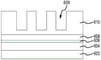
图6A示出了根据本公开的实施方案的在晶片衬底上方沉积多个电介质层的横截面视图。Figure 6A shows a cross-sectional view of depositing multiple dielectric layers over a wafer substrate according to an embodiment of the present disclosure.
图6B示出了根据本公开实施方案的蚀刻图6A的顶部电介质层以形成沟槽的横截面视图。6B illustrates a cross-sectional view of etching the top dielectric layer of FIG. 6A to form trenches according to an embodiment of the disclosure.
图6C示出了根据本公开的实施方案的在图6B的沟槽以及顶部电介质层上方沉积衬垫层(liner)和铜层的横截面视图。6C shows a cross-sectional view of depositing a liner and copper layer over the trench and top dielectric layer of FIG. 6B according to an embodiment of the disclosure.
图6D示出了根据本公开实施方案的图6C的铜层的化学机械平坦化(CMP)以暴露顶部电介质层的横截面视图。6D shows a cross-sectional view of chemical mechanical planarization (CMP) of the copper layer of FIG. 6C to expose the top dielectric layer, according to an embodiment of the disclosure.
图6E示出了根据本公开实施方案的在图6D的铜层和顶部电介质层上方沉积电介质层的横截面视图。6E shows a cross-sectional view of a dielectric layer deposited over the copper layer and top dielectric layer of FIG. 6D according to an embodiment of the disclosure.
图6F示出了根据本公开的实施方案的使用镶嵌工艺图案化在图6E的电介质层上方的铜层的横截面视图。6F shows a cross-sectional view of a copper layer patterned over the dielectric layer of FIG. 6E using a damascene process, according to an embodiment of the disclosure.
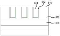
图6G示出了根据本公开的实施方案的化学蚀刻图6F的顶部电介质层以在铜柱之间形成纳米间隙的横截面视图。6G shows a cross-sectional view of chemically etching the top dielectric layer of FIG. 6F to form nanogaps between copper pillars according to an embodiment of the present disclosure.
图6H示出了根据本公开的实施方案的将电介质涂层施加到图6G的铜柱的横截面视图。Figure 6H shows a cross-sectional view of the application of a dielectric coating to the copper pillar of Figure 6G, according to an embodiment of the present disclosure.
图6I示出了根据本公开的实施方案的在铜柱上方布置电可调谐材料并且填充图6H的铜柱之间的纳米间隙的横截面视图。61 shows a cross-sectional view of disposing an electrically tunable material over copper pillars and filling the nanogap between copper pillars of FIG. 6H , according to an embodiment of the disclosure.
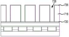
图7A示出了根据本公开的实施方案的使用镶嵌工艺形成图案化的铜柱和铜贴片的横截面视图。7A shows a cross-sectional view of patterned copper pillars and copper patches formed using a damascene process according to an embodiment of the present disclosure.
图7B示出了根据本公开的实施方案的化学蚀刻图7A的电介质层以去除顶部电介质层和导电阻挡层以在铜柱之间形成纳米间隙的横截面视图。7B shows a cross-sectional view of chemically etching the dielectric layer of FIG. 7A to remove the top dielectric layer and conductive barrier layer to form nano-gap between copper pillars according to an embodiment of the present disclosure.
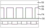
图7C示出了根据本公开实施方案的将电介质涂层施加到图7B的铜柱上的横截面视图。7C shows a cross-sectional view of the application of a dielectric coating to the copper pillar of FIG. 7B in accordance with an embodiment of the disclosure.
图7D示出了根据本公开实施方案的在铜柱上方布置电可调谐材料并且填充图7C的铜柱之间的纳米间隙的横截面视图。7D shows a cross-sectional view of disposing an electrically tunable material over copper pillars and filling the nanogap between the copper pillars of FIG. 7C , according to an embodiment of the disclosure.
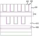
图8A示出了根据本公开的实施方案的使用镶嵌工艺形成图案化的铜柱和铜贴片的横截面视图。8A shows a cross-sectional view of patterned copper pillars and copper patches formed using a damascene process according to an embodiment of the disclosure.
图8B示出了根据本公开的实施方案化学蚀刻图8A的顶部电介质层以去除顶部电介质层,围绕铜柱的导电阻挡层以及在铜柱下方的电介质层以在铜柱之间形成纳米间隙的横截面视图。8B illustrates chemical etching of the top dielectric layer of FIG. 8A to remove the top dielectric layer, the conductive barrier layer surrounding the copper pillars, and the dielectric layer below the copper pillars to form nanogaps between the copper pillars according to an embodiment of the present disclosure. Cross-sectional view.
图8C示出了根据本公开实施方案的将电介质涂层施加到图8B的铜柱上的横截面视图。8C shows a cross-sectional view of the application of a dielectric coating to the copper pillar of FIG. 8B in accordance with an embodiment of the disclosure.
图8D示出了根据本公开的实施方案的在铜柱上方布置电可调谐材料并且填充在铜柱之间的纳米间隙以及图8C的铜柱下方的横截面视图。8D shows a cross-sectional view of disposing an electrically tunable material over copper pillars and filling the nanogap between copper pillars and below the copper pillars of FIG. 8C , according to an embodiment of the present disclosure.
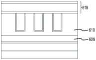
图9示出了根据本公开实施方案的来自图7D的修改结构的横截面视图。Figure 9 shows a cross-sectional view of a modified structure from Figure 7D according to an embodiment of the disclosure.
发明详细说明Detailed Description of the Invention
可以通过参考结合如下文描述的附图的以下详细描述来理解本公开。注意,出于说明清楚的目的,各个附图中的某些元件可能未按比例绘制。The present disclosure can be understood by referring to the following detailed description taken in conjunction with the accompanying drawings as described below. Note that for illustrative clarity, some elements in the various figures may not be drawn to scale.
本专利申请涉及于2018年2月22日提交的标题为“Control Circuitry andFabrication Techniques for Optical Metasurfaces”的PCT申请PCT/US18/19269,该申请的全部内容通过引用并入本文。This patent application is related to PCT Application PCT/US18/19269 entitled "Control Circuitry and Fabrication Techniques for Optical Metasurfaces," filed February 22, 2018, which is incorporated herein by reference in its entirety.
本专利申请还涉及于2018年3月19日提交的标题为“PLASMONIC SURFACE-SCATTERING ELEMENTS AND METASURFACES FOR OPTICAL BEAM STEERING”的美国专利申请号15/924,744,其全部内容通过引用并入本文。This patent application is also related to U.S. Patent Application No. 15/924,744, entitled "PLASMONIC SURFACE-SCATTERING ELEMENTS AND METASURFACES FOR OPTICAL BEAM STEERING," filed March 19, 2018, the entire contents of which are incorporated herein by reference.
总览overview
本公开提供了用于制造金属全息超表面装置的方法,该金属全息超表面装置可在更高的频率,特别是在红外或可见光频率下操作。当将工作频率放大到光学(红外/可见光)频率时,单个散射元件的大小和相邻散射元件之间的间距将按比例缩小,以保留该技术的亚波长/超材料方面。在光频率下操作的相关长度标度通常为微米或更小量级,小于常规印刷电路板(PCB)工艺的典型长度标度。The present disclosure provides methods for fabricating metal holographic metasurface devices that can operate at higher frequencies, particularly at infrared or visible light frequencies. When scaling up the operating frequency to optical (infrared/visible) frequencies, the size of individual scattering elements and the spacing between adjacent scattering elements are scaled down to preserve the subwavelength/metamaterial aspect of the technology. The relevant length scales for operation at optical frequencies are typically on the order of microns or smaller, which is smaller than typical length scales for conventional printed circuit board (PCB) processes.
金属全息超表面装置包括全息元件(hologram element)的阵列,其可以是一维(1D)阵列或二维(2D)阵列。每个全息元件都包括一对金属柱,电可调谐材料以及作为反射器的背板结构。A metal holographic metasurface device includes an array of hologram elements, which can be a one-dimensional (1D) array or a two-dimensional (2D) array. Each holographic element consists of a pair of metal pillars, an electrically tunable material, and a backplate structure that acts as a reflector.
与PCT申请PCT/US18/19269中公开的光学超表面相比,金属光学超表面包括金属柱(例如铜柱),而不是全息元件中的电介质柱。使用金属柱代替电介质柱有很多好处。In contrast to the optical metasurfaces disclosed in PCT application PCT/US18/19269, metallic optical metasurfaces include metal pillars, such as copper pillars, rather than dielectric pillars as in holographic elements. There are many benefits to using metal posts instead of dielectric posts.
在光学上,金属柱减少了金属全息超表面的全息元件之间的耦合。金属柱不允许光场从电可调谐材料穿透,使得光场基本上被限制在电可调谐材料内。结果,金属柱将阵列中的全息元件彼此隔离,并减小了全息元件之间的光学耦合。相反,电介质柱(例如非晶硅柱)允许光场从电可调谐材料穿透到柱中,使得全息元件耦合在一起。Optically, the metal pillars reduce the coupling between the holographic elements of the metal holographic metasurface. The metal posts do not allow the optical field to penetrate from the electrically tunable material such that the optical field is substantially confined within the electrically tunable material. As a result, the metal posts isolate the holographic elements in the array from each other and reduce optical coupling between the holographic elements. In contrast, dielectric pillars, such as amorphous silicon pillars, allow the optical field to penetrate from the electrically tunable material into the pillars, allowing the holographic elements to couple together.
在电学上,金属柱是比非晶硅柱更好的导体。因此,金属光学超表面具有比具有电介质柱的光学超表面小的欧姆损耗。金属柱可以尤其包括铜,金,银,铝。Electrically, metal pillars are better conductors than amorphous silicon pillars. Therefore, metallic optical metasurfaces have smaller ohmic losses than optical metasurfaces with dielectric pillars. Metal pillars may include copper, gold, silver, aluminum, among others.
本公开内容涉及用于制造铜全息超表面的镶嵌工艺,其包括铜柱阵列,所述铜柱阵列具有填充在铜柱之间的纳米级间隙中的电可调谐材料。The present disclosure relates to a damascene process for fabricating a copper holographic metasurface comprising an array of copper pillars with an electrically tunable material filled in the nanoscale gaps between the copper pillars.
本公开提供使用镶嵌工艺来图案化铜柱的方法。已经开发出镶嵌工艺来制造半导体集成电路,该半导体集成电路使用铜来互连金属化层中的晶体管。The present disclosure provides methods for patterning copper pillars using a damascene process. Damascene processes have been developed to fabricate semiconductor integrated circuits that use copper to interconnect transistors in metallization layers.
本公开提供了用于添加电介质阻挡层以保护铜免于扩散的方法。阻挡层还可以防止铜腐蚀。这与电子设备或半导体集成电路完全不同。在电子器件中,包括Ta和/或TaN的导电阻挡层用于防止铜扩散到绝缘体中。包括Ta和/或TaN的导电阻挡层有助于保护铜免于扩散到绝缘体中,并且还电连接至两个铜层。另一方面,用于铜的电介质阻挡层将不起作用,因为电介质层阻止了两个铜层的电连接。The present disclosure provides methods for adding a dielectric barrier layer to protect copper from diffusion. The barrier layer also prevents copper corrosion. This is completely different from electronic devices or semiconductor integrated circuits. In electronic devices, conductive barrier layers comprising Ta and/or TaN are used to prevent copper from diffusing into the insulator. A conductive barrier layer comprising Ta and/or TaN helps protect the copper from diffusing into the insulator and also electrically connects the two copper layers. On the other hand, a dielectric barrier layer for copper will not work because the dielectric layer prevents the electrical connection of the two copper layers.
本公开还提供了用于向铜添加包括Ta和/或TaN的导电阻挡层,但是然后去除一部分导电阻挡层以减少由于导电阻挡层引起的光学损失并用电介质阻挡层重新涂覆铜的方法。除去Ta和/或TaN的原因是,Ta和TaN在感兴趣的频率范围内对光的吸收能力非常强。Ta和TaN的存在将影响金属光学超表面的光学性能,但是不影响电路的电性能。The present disclosure also provides methods for adding a conductive barrier layer comprising Ta and/or TaN to copper, but then removing a portion of the conductive barrier layer to reduce optical loss due to the conductive barrier layer and recoating the copper with a dielectric barrier layer. The reason for removing Ta and/or TaN is that Ta and TaN absorb light very strongly in the frequency range of interest. The presence of Ta and TaN will affect the optical performance of the metal optical metasurface, but not the electrical performance of the circuit.
一种方法还可以包括用电可调谐材料填充铜柱之间的纳米间隙以形成金属光学超表面装置。电可调谐材料尤其可以包括液晶,电光(EO)聚合物材料或硫系化物玻璃。该电可调谐材料的折射率可以通过施加电压来调整。A method may also include filling the nanogap between the copper pillars with an electrically tunable material to form a metal optical metasurface device. Electrically tunable materials may include liquid crystals, electro-optic (EO) polymer materials or chalcogenide glasses, among others. The refractive index of the electrically tunable material can be tuned by applying a voltage.
金属光学超表面metal optical metasurface
图1A示出了根据本公开的实施方案的金属全息超表面装置的俯视图。如图1A所示,金属全息超表面装置100具有金属全息超表面区域102,其包括在基底108的第一部分上的全息元件的阵列,这在图1B中可以看到。金属全息超表面区域102包括全息元件的阵列。每个全息元件包括一对金属柱和在该对金属柱之间的折射率可调谐芯材料(即,电可调谐材料)。FIG. 1A shows a top view of a metal holographic metasurface device according to an embodiment of the present disclosure. As shown in FIG. 1A , a metal
全息超表面装置100还可在芯片的第二部分上具有包括CMOS晶体管的互连区域103,互连区域103中的CMOS晶体管可以控制施加到每个全息元件的金属柱的电压。CMOS晶体管具有低的静态功耗和高的抗干扰度。全息元件阵列和电气控制电路是解耦的(decoupled)。在一些实施方案中,互连区域103可以包括没有有源元件的导线的复杂布线。The
在一些实施方案中,互连区域可以至少部分地混合在全息超表面(未示出)内。例如,金属全息超表面可以具有主动控制,其中电路部分在全息表面下方。In some embodiments, interconnect regions can be at least partially intermingled within a holographic metasurface (not shown). For example, metal holographic metasurfaces can have active control, where the circuit part is underneath the holographic surface.
图1B是根据本公开的实施方案的1D金属全息超表面装置的横截面视图。如图1B所示,阵列102包括线性排列在晶片上的多列金属全息元件106。金属全息元件或谐振器106包括一对金属柱110A-110B和在金属柱之间的电可调谐材料112。金属柱沉积在背板结构104上。在一些实施方案中,背板结构104可以尤其包括完整背板(full backplane),部分背板,凹口设计或布拉格反射器中的一种。Figure IB is a cross-sectional view of a 1D metal holographic metasurface device according to an embodiment of the disclosure. As shown in FIG. 1B,
入射波的掠入射(例如图1B中所示的激光输入)以较高的Q因子激发金属柱之间的间隙中的共振,从而实现了相位的动态调制。另外,金属柱沉积在背板结构上,这使得该结构用作反射阵列,因此可以与控制电子器件集成。谐振器包括两个金属柱,它们由具有可调谐折射率的电可调谐材料分隔开。谐振器产生如图1B所示的全息输出。Grazing incidence of incident waves (such as the laser input shown in Figure 1B) excites resonances in the gaps between metal pillars with a high Q factor, enabling dynamic modulation of the phase. In addition, metal pillars are deposited on the backplane structure, which allows the structure to act as a reflective array and thus can be integrated with the control electronics. The resonator consists of two metal pillars separated by an electrically tunable material with a tunable refractive index. The resonator produces a holographic output as shown in Figure 1B.
金属柱的反射相位对芯材料的折射率敏感,可能具有接近2π的相位调制,其中Δn/n的折射率调制约为7%。共振的高Q(例如Q为20)可实现对芯材料折射率的高灵敏度。反射相位对所述芯的折射率的高灵敏度可使折射率可调谐芯材料集成到金属柱之间的间隙中,以创建动态的超表面。The reflection phase of the metal pillars is sensitive to the refractive index of the core material, possibly with a phase modulation close to 2π, where the refractive index modulation of Δn/n is about 7%. The high Q of the resonance (eg, Q of 20) enables high sensitivity to the refractive index of the core material. The high sensitivity of the reflection phase to the refractive index of the core enables the integration of index-tunable core materials into the gaps between metal pillars to create dynamic metasurfaces.
由于可调谐(tunable)电介质材料的折射率调制范围可能很小,因此设计可调谐辐射或散射元件阵列的一个挑战是创建高Q因子,低损耗的亚波长谐振器。Q因子是一个无因次参数,用于表征谐振器相对于其中心频率的带宽。高Q因子表示相对于谐振器存储的能量而言,能量损失率较低。具有高Q因子的谐振器具有较低的阻尼。One challenge in designing arrays of tunable radiating or scattering elements is the creation of high-Q factor, low-loss subwavelength resonators due to the potentially small range of refractive index modulation of tunable dielectric materials. The Q factor is a dimensionless parameter that characterizes the bandwidth of a resonator relative to its center frequency. A high Q factor indicates a low rate of energy loss relative to the energy stored in the resonator. A resonator with a high Q factor has lower damping.
背板结构104沉积在基底108上,用于支撑金属柱。在一些实施方案中,基底108可以包括晶片衬底,其尤其是可以是晶体硅晶片。在一些实施方案中,基底108可包括晶片衬底以及用于导线的多个层。A
背板结构104反射光波。在两个金属柱202上施加控制电压以在全息元件106A上产生静电场。电场和磁场都很好地限制于在两个金属柱110A-110B之间的纳米间隙中的电可调谐材料112。The
图2示出了根据本公开的实施方案的图1B的阵列中具有谐振器的亚波长全息元件106A之一的横截面视图,该谐振器包括一对金属柱和完整的背板结构。如图所示,金属全息元件106A(例如亚波长金属全息元件)包括谐振器,该谐振器具有在背板结构104A上方的两个金属柱202之间的电可调谐材料或折射率可调谐材料204,背板结构104A位于基底108和金属柱202A-B之间。完整背板结构104A可以包括在金属层208上方的电介质层206,如图2所示。电介质间隔物206可以包括至少一个薄的耐化学腐蚀层和至少一个厚的电介质层。2 shows a cross-sectional view of one of the subwavelength
电场和磁场都被很好地限制在两个金属柱202A-202B之间的纳米间隙中的电可调谐材料204中。电场和磁场主要限制在谐振器的顶端和底端之间。Both electric and magnetic fields are well confined within the electrically
图3示出了根据本公开的实施方案的图1B的阵列中具有谐振器的亚波长全息元件106B之一的横截面视图,该谐振器包括一对金属柱和部分背板结构。如图所示,金属全息元件106B(例如是亚波长金属全息元件)包括谐振器,该谐振器具有在背板结构104B上方的两个金属柱302之间的折射率可调谐材料304,背板结构104B位于基底108和金属柱302A-B之间。部分背板结构104B可以包括嵌入在电介质层306中的金属贴片308。金属贴片308可以是矩形的,其具有标记为H_m的高度和标记为W_m的宽度。金属贴片308位于电可调谐材料304下方。金属贴片308的宽度可以从零变化到接近节距(pitch)。当金属贴片的宽度等于节距时,部分背板结构变为完整背板结构。3 shows a cross-sectional view of one of the subwavelength
当金属贴片由铜形成时,可以通过考虑宽度对制造和光学性能的影响来设计铜贴片的宽度。一方面,更容易制造具有减小的铜贴片宽度的铜贴片。另一方面,当铜贴片的宽度增加时,光学性能变得更好。When the metal patch is formed of copper, the width of the copper patch can be designed by considering the effect of the width on manufacturing and optical performance. On the one hand, it is easier to manufacture copper patches with reduced copper patch widths. On the other hand, when the width of the copper patch increases, the optical performance becomes better.
再次,电场和磁场都很好地限制于在两个金属柱302A-B之间的纳米间隙中的电可调谐材料304。电场和磁场都主要限制在谐振器的顶端和底端之间。Again, both electric and magnetic fields are well confined to the electrically
图4示出了根据本公开的实施方案的在图1B的阵列中具有谐振器的亚波长全息元件106C之一的横截面视图,该谐振器包括一对金属柱和凹口设计背板结构。如图所示,金属全息元件106C(例如亚波长金属全息元件)包括谐振器,该谐振器具有在背板结构上方的两个金属柱402之间的折射率可调谐材料404,背板结构位于基底108和金属柱402A-B之间。4 shows a cross-sectional view of one of the subwavelength
凹口设计背板结构104C可以包括电介质层406,电介质层406具有在金属层408上方的凹口410。凹口410位于纳米间隙中的电可调谐材料404之下。凹口410连接到电介质层406并突出到金属层408中。该凹口可以通过在电介质间隔物的位置处的磁场中施加节点来防止单位晶格(unit cell)之间的耦合。Notch Design The
同样,电场和磁场都很好地限制于在两个金属柱402A-B之间的纳米间隙中的电可调谐材料404中。电场和磁场主要限制在谐振器的顶端和底端之间。Also, both electric and magnetic fields are well confined in the electrically
图5示出了在根据本公开的实施方案的图1B的阵列中具有谐振器的亚波长全息元件106D之一的横截面视图,该谐振器包括一对金属柱和布拉格反射器背板结构。如图所示,金属全息元件106D(例如亚波长金属全息元件)包括谐振器,该谐振器具有在背板结构上方的两个金属柱502A-B之间的折射率可调谐材料504,背板结构位于基底108和金属柱502A-B之间。5 shows a cross-sectional view of one of the subwavelength
布拉格反射器背板结构104D可以包括多个电介质层,多个电介质层交错地具有具有低电介质指数的电介质层506A和具有高电介质指数的电介质层506B。布拉格反射器背板结构104D是非金属反射器。The Bragg
同样,电场和磁场都很好地限制于在两个金属柱502A-B之间的纳米间隙中的电可调谐材料504中。电场和磁场大多被限制在谐振器106D的顶端和底端之间。Also, both electric and magnetic fields are well confined in the electrically
在上述金属全息元件106A-D的谐振器中,节点或腹点(anti-node)的数量可以随着金属柱的高度而变化。例如,对于金属柱的高度,在电场中存在两个节点或两个腹点,且在磁场中存在两个节点或两个腹点。当包括金属柱和电可调谐材料的谐振器的高度减小时,谐振器可以仅具有一个谐振。当谐振器的高度增加时,谐振器可以具有三个,四个或更多节点。In the resonators of metal
在制造期间完成高度的调整。一旦谐振器的高度固定,就可以围绕谐振调整背板结构。然后,可以调整可调谐材料的折射率。The height adjustment is done during manufacture. Once the height of the resonator is fixed, the backplane structure can be tuned around resonance. Then, the refractive index of the tunable material can be tuned.
作为示例,表1列出了如图3所示的谐振器和部分背板结构的节距,高度和宽度的尺寸。作为示例,电介质层306是SiO2。As an example, Table 1 lists the pitch, height and width dimensions of the resonator and part of the backplane structure shown in FIG. 3 . As an example,
表1:金属全息元件的尺寸Table 1: Dimensions of metal holographic elements
表1中的特定尺寸适用于905nm的工作波长。这些尺寸可能随波长而变化。例如,在1550nm的波长下,参数应乘以等于两个波长之比的系数,即1550/905。The specific dimensions in Table 1 are for an operating wavelength of 905nm. These dimensions may vary with wavelength. For example, at a wavelength of 1550nm, the parameter should be multiplied by a factor equal to the ratio of the two wavelengths, ie 1550/905.
对于完整的背板结构104A和布拉格反射器背板结构104D,节距是宽度(W_m)。For the
对于凹口设计背板结构104C,凹口具有W_slot的宽度,并且在905nm的波长处的深度是在100nm至150nm的范围内。For the notch
本领域技术人员将意识到,高度,宽度和节距的尺寸可以变化。Those skilled in the art will appreciate that dimensions of height, width and pitch may vary.
镶嵌工艺Mosaic technology
已经开发出镶嵌工艺以制造半导体集成电路,该半导体集成电路使用铜来互连金属化层中的晶体管。在半导体芯片的制造中,通过镶嵌工艺对铜进行图案化。这是因为不能通过已经成功地与铝一起使用的光致抗蚀剂掩模和等离子体蚀刻的已知技术来对铜进行图案化。在本领域中已知铜是比铝更好的导体。因此,使用铜基芯片的半导体芯片可以具有较小的金属组件,并使用较少的电能,并可以得到性能更高的处理器。由于具有优于铝的这些优点,因此在镶嵌工艺中已进行了巨大的开发工作。Damascene processes have been developed to fabricate semiconductor integrated circuits that use copper to interconnect transistors in metallization layers. In the manufacture of semiconductor chips, copper is patterned by a damascene process. This is because copper cannot be patterned by the known techniques of photoresist masking and plasma etching that have been used successfully with aluminum. Copper is known in the art to be a better conductor than aluminum. As a result, semiconductor chips using copper-based chips can have smaller metal components and use less power, leading to higher-performance processors. Because of these advantages over aluminum, a huge development effort has been done in damascene technology.
在镶嵌工艺中,利用在其中填充导体的沟槽对下面的电介质绝缘层(例如,氧化硅)进行图案化。厚的铜层涂层填充满沟槽并沉积在绝缘层上。然后,使用化学机械平坦化(CMP)去除在绝缘层的顶表面上方延伸的铜以进行平坦化。电介质绝缘层的沟槽内的铜成为图案化导体。In a damascene process, the underlying dielectric insulating layer (eg, silicon oxide) is patterned with trenches filled with conductors. A thick layer of copper coating fills the trenches and is deposited on top of the insulating layer. Copper extending over the top surface of the insulating layer is then removed for planarization using chemical mechanical planarization (CMP). The copper in the trenches of the dielectric insulating layer becomes the patterned conductor.
镶嵌工艺可以是单镶嵌工艺或双镶嵌工艺。在一些实施方案中,单镶嵌工艺可以包括两个单独的镶嵌步骤,其可以用于分别形成沟槽和通孔。此单镶嵌工艺可用于形成不存在通孔的器件。The damascene process can be a single damascene process or a dual damascene process. In some embodiments, a single damascene process may include two separate damascene steps, which may be used to form trenches and vias, respectively. This single damascene process can be used to form devices without vias.
在一些实施方案中,双镶嵌工艺组合形成两个特征以减少工艺步骤的数量。双镶嵌工艺通常同时形成并填充两个特征,例如使用单个铜沉积形成覆盖通孔的沟槽。利用绝缘体和铜的连续层,创建了多层互连结构。In some embodiments, the dual damascene process combines to form two features to reduce the number of process steps. The dual damascene process typically forms and fills two features simultaneously, such as using a single copper deposition to form a trench covering a via. Using successive layers of insulator and copper, a multilayer interconnect structure is created.
除了对步骤数量的简化之外,双镶嵌工艺和单镶嵌工艺在很大程度上是相同的。本领域技术人员将知道,在单镶嵌工艺中任何可能的事情都可能在双镶嵌工艺中实现。Apart from the simplification of the number of steps, the dual damascene process is largely the same as the single damascene process. Those skilled in the art will know that anything that is possible in a single damascene process is possible in a dual damascene process.
在镶嵌工艺中,导电阻挡层完全包围所有铜互连。导电阻挡层防止铜扩散到任何周围的材料中,这会降低周围材料的性能。例如,硅在掺杂铜后会形成深能级陷阱。导电阻挡层可充分降低铜的扩散率,因此将铜与电介质绝缘体(例如,氧化硅)化学隔离,同时仍具有高导电率以维持良好的电子接触。In the damascene process, the conductive barrier completely surrounds all copper interconnects. The conductive barrier layer prevents copper from diffusing into any surrounding material, which would degrade the performance of the surrounding material. Silicon, for example, forms deep level traps when doped with copper. The conductive barrier layer can sufficiently reduce the diffusivity of copper, thus chemically isolating the copper from the dielectric insulator (eg, silicon oxide), while still having high conductivity to maintain good electronic contact.
导电阻挡层或膜可以不太厚,使得两个导电阻挡膜和铜导体的堆叠的总电阻可以超过铝互连的电阻。在一些实施方案中,将导电阻挡层添加在铜导体的所有四个侧面部分上以减少扩散。在一些实施方案中,导电阻挡层被施加到侧面部分和底部,以及顶表面通常是电介质阻挡层而不是Ta/TaN阻挡层。典型的阻挡金属尤其包括Ta和TaN。The conductive barrier layer or film may not be so thick that the total resistance of the stack of two conductive barrier films and the copper conductor may exceed the resistance of the aluminum interconnect. In some embodiments, a conductive barrier layer is added on all four side portions of the copper conductor to reduce diffusion. In some embodiments, a conductive barrier layer is applied to the side portions and bottom, and the top surface is typically a dielectric barrier layer rather than a Ta/TaN barrier layer. Typical barrier metals include Ta and TaN, among others.
金属光学超表面的制造Fabrication of metal optical metasurfaces
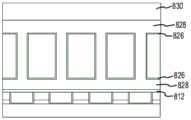
实施例1Example 1
图6A-6I提供了使用镶嵌工艺形成金属光学超表面的步骤。如图2所示,金属光学超表面包括作为反射器的部分背板结构。该方法包括制造包括铜贴片的部分背板结构。该方法还包括形成具有电介质阻挡层(例如,氮化物层)的图案化铜柱。该方法用用于铜全息超表面的电介质阻挡层代替了常规镶嵌工艺中通常使用的导电阻挡层(例如,Ta和/或钽氮化物)。该方法还包括用电介质涂层(例如,氮化物层)重新涂覆铜柱,以防止铜迁移到电介质绝缘体层(例如,氧化硅)中。该方法还包括用电可调谐材料填充铜柱之间的纳米间隙。Figures 6A-6I provide steps for forming a metallic optical metasurface using a damascene process. As shown in Fig. 2, the metallic optical metasurface includes a partial backplate structure as a reflector. The method includes fabricating a portion of the backplane structure including copper patches. The method also includes forming a patterned copper pillar with a dielectric barrier layer (eg, a nitride layer). This method replaces the conductive barrier layer (eg, Ta and/or tantalum nitride) typically used in conventional damascene processes with a dielectric barrier layer for the copper holographic metasurface. The method also includes recoating the copper pillars with a dielectric coating (eg, a nitride layer) to prevent migration of copper into the dielectric insulator layer (eg, silicon oxide). The method also includes filling the nanogap between the copper pillars with an electrically tunable material.
图6A示出根据本发明的实施方案的在晶片衬底上方沉积多个电介质层的横截面视图。如图6A所示,将电介质层604、606、608和610的堆叠沉积在晶片衬底602上方。电介质层尤其可以包括电介质材料,例如氮化硅(SiN),硅碳氮(SiCN),碳化硅(SiC),氧化铝(Al2O3),二氧化铪(HfO2),氧化硅(SiO2)。沉积技术尤其可以包括物理气相沉积(PVD),化学气相沉积(CVD)或等离子体增强化学气相沉积(PECVD)。Figure 6A shows a cross-sectional view of depositing multiple dielectric layers over a wafer substrate in accordance with an embodiment of the present invention. As shown in FIG. 6A , a stack of
图6B-6D示出了形成包括铜贴片的部分背板结构的步骤。图6B示出了根据本公开实施方案的蚀刻图6A的顶部电介质层以形成沟槽的横截面视图。如图6B所示,通过干法蚀刻或等离子蚀刻在顶部电介质层610中形成沟槽609。干蚀刻或等离子蚀刻可以在垂直方向上蚀刻,使得可以在电介质层中形成垂直沟槽。6B-6D illustrate the steps of forming a portion of the backplane structure including copper patches. 6B illustrates a cross-sectional view of etching the top dielectric layer of FIG. 6A to form trenches according to an embodiment of the disclosure. As shown in FIG. 6B,
图6C示出了根据本公开实施方案的在图6B的沟槽以及顶部电介质层上方沉积衬垫层和铜层的横截面视图。如图所示,铜沉积在衬垫层612上。铜层614被衬垫层612保护。衬垫层612尤其可以是导电阻挡材料,例如Ta和/或TaN。6C shows a cross-sectional view of depositing a liner layer and a copper layer over the trench and top dielectric layer of FIG. 6B according to an embodiment of the disclosure. Copper is deposited on
可以将铜层电镀到涂覆有衬垫层612的沟槽中。电镀沉积可以是两步过程。可以首先使用物理气相沉积(PVD)沉积籽晶层,然后将铜电镀在籽晶层上。A layer of copper may be electroplated into the trenches coated with
图6D示出了根据本公开实施方案的图6C的铜层的化学机械平坦化(CMP)以暴露顶部电介质层的横截面视图。如图6D所示,通过使用CMP来平坦化铜层来形成铜贴片614。铜贴片嵌入顶部电介质层610内。6D shows a cross-sectional view of chemical mechanical planarization (CMP) of the copper layer of FIG. 6C to expose the top dielectric layer, according to an embodiment of the disclosure. As shown in FIG. 6D , a
图6E示出了根据本公开的实施方案的在图6D的铜层和顶部电介质层上方沉积电介质层的横截面视图。如图所示,电介质间隔物618沉积在平坦化的铜贴片614和电介质层610上方。6E shows a cross-sectional view of a dielectric layer deposited over the copper layer and top dielectric layer of FIG. 6D according to an embodiment of the disclosure. As shown, a
电介质间隔物可以包括多个电介质层。作为示例,电介质间隔物可以包括顶部氮化物层,底部氮化物层以及在顶部氮化物层和底部氮化物层之间的氧化物层。电介质间隔物可以包括电介质材料,例如SiN,SiCN,SiC,Al2O3,HfO2,SiO2等。沉积技术可以包括PVD,CVD或PECVD等。本领域技术人员将理解,电介质间隔物的材料和厚度可以变化。A dielectric spacer may include multiple dielectric layers. As an example, a dielectric spacer may include a top nitride layer, a bottom nitride layer, and an oxide layer between the top nitride layer and the bottom nitride layer. The dielectric spacers may include dielectric materials such as SiN, SiCN, SiC, Al2 O3 , HfO2 , SiO2 and the like. Deposition techniques can include PVD, CVD or PECVD, among others. Those skilled in the art will appreciate that the material and thickness of the dielectric spacers can vary.
图6F示出了根据本公开的实施方案的使用镶嵌工艺图案化图6E的电介质层上方的铜层的横截面视图。如图所示,铜柱622之间形成有纳米间隙。电介质阻挡层620覆盖铜柱622的侧壁和底部。电介质层624填充铜柱之间的纳米间隙中的空间。电介质阻挡层620是光学透明的,并且可以包括电介质材料,例如氮化硅(SiN),硅碳氮(SiCN),碳化硅(SiC),氧化铝(Al2O3),二氧化铪(HfO2),氧化硅(SiO2)和阻挡铜扩散的光学透明材料等。6F illustrates a cross-sectional view of patterning a copper layer over the dielectric layer of FIG. 6E using a damascene process, according to an embodiment of the disclosure. As shown, nanogaps are formed between the
在一些实施方案中,镶嵌工艺可以是双镶嵌工艺,其可以包括在铜柱622和铜贴片614中的元件之间进行电通孔连接。如果将电介质衬垫层用于电介质阻挡层620,则这些连接是不可能的,并且可以与IC区域中的另一层中的铜柱622的顶侧进行电接触。In some embodiments, the damascene process may be a dual damascene process, which may include making electrical via connections between
在一些实施方案中,由于只有一个蚀刻步骤,因此6A-F的顺序描绘了单镶嵌工艺。如果该工艺是双镶嵌工艺,则可能会进行另一次如图6B所示操作的蚀刻,蚀刻进行到不同的深度。而且,对于双镶嵌工艺,在图6B和图6C之间可能会有湿法蚀刻步骤,以暴露出下面的Cu。In some embodiments, the sequence of 6A-F depicts a single damascene process since there is only one etch step. If the process is a dual damascene process, another etch may be performed as shown in Figure 6B, to a different depth. Also, for a dual damascene process, there may be a wet etch step between FIG. 6B and FIG. 6C to expose the underlying Cu.
该方法包括在电介质层624中形成沟槽和通孔(未示出)。通孔连接到铜柱,以向铜柱施加电压。The method includes forming trenches and vias (not shown) in the
该方法包括在沟槽上方沉积电介质阻挡层620,如图6F所示。该方法不同于常规的用于半导体集成电路芯片的制造方法,其中,通常将导电阻挡层(例如Ta/TaN)施加到沟槽上,例如如图6C所示。The method includes depositing a
该方法还包括通过电镀在沟槽上方沉积铜层,然后进行CMP以形成铜贴片622。The method also includes depositing a copper layer over the trenches by electroplating, followed by CMP to form
在一些实施方案中,通孔可以不存在于金属光学超表面的全息表面中,例如如图1A所示。在替代实施方案中,通孔可以存在于有源金属光学超表面(未示出)中,或者存在于金属光学超表面的互连区域103中。使用双镶嵌工艺形成通孔和沟槽。在单个沉积操作中,铜同时沉积在通孔和沟槽中。In some embodiments, vias may not be present in the holographic surface of the metal optical metasurface, eg, as shown in FIG. 1A . In alternative embodiments, vias may be present in the active metal optical metasurface (not shown), or in the
图6G示出了根据本公开的实施方案的化学蚀刻图6F的顶部电介质层以在铜柱之间形成纳米间隙的横截面视图。如图所示,使用例如缓冲氧化物蚀刻剂(BOE)之类的蚀刻剂通过化学蚀刻来去除铜柱622之间的电介质层624。与等离子体蚀刻不同,化学蚀刻可以在所有方向上进行蚀刻。蚀刻剂可以蚀刻一种电介质材料,例如氧化物,但是可以不蚀刻另一相邻的电介质材料,例如氮化物。6G shows a cross-sectional view of chemically etching the top dielectric layer of FIG. 6F to form nanogaps between copper pillars according to an embodiment of the present disclosure. As shown, the
另外,如图6G所示,蚀刻剂除去铜柱622的垂直侧壁上的电介质阻挡层620,而底部电介质阻挡层620保留在铜柱622和铜柱622下方的电介质层618之间。Additionally, as shown in FIG. 6G , the etchant removes the
图6H示出了根据本公开实施方案的将电介质涂层施加至图6G的铜柱的横截面视图。如图6H所示,电介质涂层625沉积在平坦化的铜柱622的顶部和侧面部分上。电介质涂层625也沉积在铜柱622之间的电介质层618的暴露的顶部上。6H shows a cross-sectional view of the application of a dielectric coating to the copper pillar of FIG. 6G in accordance with an embodiment of the disclosure. As shown in FIG. 6H , a
可以通过使用原子层沉积(ALD)或等离子体增强化学气相沉积(PECVD)来施加电介质涂层625。电介质涂层625是光学透明的,并且可以包括电介质材料,例如SiN,SiCN,SiC,Al2O3,HfO2,SiO2以及阻挡铜扩散的光学透明材料等。可以非常快速地施加电介质涂层625,以在没有任何保护层的情况下使铜的暴露最小。
图6I示出了根据本公开的实施方案在图6H的铜柱上方布置电可调谐材料并且填充的铜柱之间的纳米间隙的横截面视图。如图所示,电可调谐材料626填充铜柱622之间的纳米间隙623。在该实施方案中,电可调谐材料626覆盖电介质涂层625的顶部。61 shows a cross-sectional view of nanogap between copper pillars filled with an electrically tunable material disposed over the copper pillars of FIG. 6H according to an embodiment of the present disclosure. As shown, electrically
在替代实施方案中,电可调谐材料626可以不覆盖电介质涂层626的顶部。电可调谐材料可以包括液晶。可以将电可调谐材料旋涂到纳米间隙中。In alternative embodiments, the electrically
该方法进一步包括用诸如玻璃和聚合物之类的光学透明材料包封(encapsulating)电可调谐材料。聚合物可以包括聚(甲基丙烯酸甲酯)(PMMA)或聚碳酸酯(PC)等。The method further includes encapsulating the electrically tunable material with optically transparent materials such as glass and polymers. The polymer may include poly(methyl methacrylate) (PMMA) or polycarbonate (PC), among others.
实施例2Example 2
本公开内容还提供了在镶嵌工艺中去除导电阻挡层(例如,Ta和/或TaN)的至少一部分并且为铜全息超表面施加电介质涂层的方法。Ta和/或TaN阻挡材料在全息超表面的频率范围内对光的吸收能力非常强。由于存在Ta和TaN阻挡层,铜光学超表面的效率非常低或几乎为零。本公开内容确定了该问题并且提供了通过去除Ta和TaN阻挡层来解决该问题的解决方案。The present disclosure also provides methods of removing at least a portion of the conductive barrier layer (eg, Ta and/or TaN) and applying a dielectric coating for the copper holographic metasurface in a damascene process. Ta and/or TaN blocking materials have very strong light absorption capabilities in the frequency range of the holographic metasurface. The efficiency of copper optical metasurfaces is very low or almost zero due to the presence of Ta and TaN barrier layers. The present disclosure identifies this problem and provides a solution to address it by removing the Ta and TaN barrier layers.
图7A示出了根据本公开的实施方案使用镶嵌工艺形成图案化的铜柱和铜贴片的横截面视图。如图所示,在部分背板结构上形成具有导电阻挡层720(例如Ta和/或TaN)的铜柱718,该部分背板结构包括电介质间隔物,电介质间隔物具有在基底702上方的各自的底部电介质层712,中间电介质层714和顶部电介质层716,铜贴片704,导电阻挡层706(例如Ta和/或TaN)。顶部电介质层722填充涂覆的铜柱718之间的纳米间隙。铜贴片704与电介质层708和710一起嵌入电介质层712下方。导电阻挡层(例如,Ta和/或TaN)沉积在铜上,以密封铜防止其扩散。Ta和TaN层可以通过溅射沉积。7A shows a cross-sectional view of patterned copper pillars and copper patches formed using a damascene process according to an embodiment of the present disclosure. As shown,
图7B示出了根据本公开的实施方案化学蚀刻图7A的电介质层以去除顶部电介质层和导电阻挡层以在铜柱之间形成纳米间隙的横截面视图。如图7B所示,根据要蚀刻的电介质材料,通过使用诸如BOE之类的蚀刻剂化学蚀刻掉电介质层722。而且,铜柱718的侧壁上的导电阻挡层被化学蚀刻掉,例如用与用于蚀刻电介质层722相同的蚀刻剂化学蚀刻掉。7B shows a cross-sectional view of chemically etching the dielectric layer of FIG. 7A to remove the top dielectric layer and conductive barrier layer to form nano-gap between copper pillars according to an embodiment of the present disclosure. As shown in FIG. 7B, the
图7C示出了根据本公开实施方案将电介质涂层施加到图7B的铜柱上的横截面视图。如图7C所示,电介质涂层726沉积在铜柱718上以保护铜柱免于扩散和/或腐蚀。该步骤也可以称为钝化操作。在涂覆的铜柱718之间形成纳米间隙728。7C shows a cross-sectional view of a dielectric coating applied to the copper pillar of FIG. 7B according to an embodiment of the disclosure. As shown in Figure 7C, a
图7D示出了根据本公开实施方案在图7C铜柱上方布置电可调谐材料并且填充铜柱之间的纳米间隙的横截面视图。如图7D所示,电可调谐材料730填充纳米间隙728并且还覆盖铜柱718的顶部。光学透明层732设置在电可调谐材料730上方。光学透明层732可以包括玻璃,聚合物。等等。例如,一块坚固的玻璃或玻璃盖可以覆盖电可调谐材料730作为保护层。7D shows a cross-sectional view of disposing an electrically tunable material over the copper pillars of FIG. 7C and filling the nanogap between the copper pillars, according to an embodiment of the disclosure. As shown in FIG. 7D , electrically
在替代实施方案中,电可调谐材料仅填充铜柱之间的纳米间隙,而不存在于铜柱的顶部。因此,光学透明层直接设置在涂覆的铜柱和电可调谐材料上方。In an alternative embodiment, the electrically tunable material only fills the nanogap between the copper pillars, and is not present on top of the copper pillars. Thus, an optically transparent layer is disposed directly over the coated copper pillars and electrically tunable material.
实施例3Example 3
本公开还提供了替代实施方案,其中金属光学超表面还去除了铜柱下方的导电阻挡层720,这减小了铜柱下方的导电阻挡层720的光吸收,如图7D所示。The present disclosure also provides an alternative embodiment in which the metal optical metasurface also removes the
图8A-8D示出了形成替代的金属光学超表面的步骤。图8A示出了根据本公开的实施方案使用镶嵌工艺形成图案化的铜柱和铜贴片的横截面视图。如图所示,在部分背板结构上形成具有导电阻挡层820(例如Ta和/或TaN)的铜柱818,该部分背板结构包括电介质间隔物,电介质间隔物具有在基底802上方的各自的电介质层812、814和816,铜贴片804,导电阻挡层806(例如Ta和/或TaN)。该基底可以包括晶片衬底等等。顶部电介质层822填充涂覆的铜柱818之间的纳米间隙。铜贴片804与电介质层808和810一起嵌入电介质层812下方。导电阻挡层(例如Ta和/或TaN)可以是通过溅射沉积在铜上。8A-8D illustrate steps in forming an alternative metallic optical metasurface. 8A shows a cross-sectional view of patterned copper pillars and copper patches formed using a damascene process according to an embodiment of the present disclosure. As shown,
图8B示出了根据本公开实施方案化学蚀刻图8A的顶部电介质层以去除顶部电介质层,围绕铜柱的导电阻挡层和铜柱下方的电介质层,以在铜柱之间形成纳米间隙的横截面视图。如图8B所示,通过使用蚀刻剂的化学蚀刻去除顶部电介质层822。铜柱下面的两个电介质层814和816也通过化学蚀刻去除。而且,从铜柱818的侧壁和底部完全去除了导电阻挡层820。8B illustrates chemically etching the top dielectric layer of FIG. 8A to remove the top dielectric layer, the conductive barrier layer surrounding the copper pillars, and the dielectric layer below the copper pillars to form a lateral width of the nanogap between the copper pillars according to an embodiment of the present disclosure. Section view. As shown in FIG. 8B, the
铜柱可以通过其他机械方式支撑。例如,可以通过规则间隔的通孔连接来提供机械支撑。这些通孔连接到接地层(ground plane layer)中的锚固特征,该锚固特征与反射器特征电气隔离。Copper pillars can be supported by other mechanical means. For example, mechanical support may be provided by regularly spaced through-hole connections. These vias connect to anchor features in the ground plane layer that are electrically isolated from the reflector features.
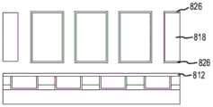
图8C示出了根据本公开实施方案将电介质涂层施加到图8B的铜柱上的横截面视图。如图所示,电介质涂层826沉积在每个铜柱的四个侧面部分周围,包括铜柱818的顶部,侧壁和底部。8C shows a cross-sectional view of a dielectric coating applied to the copper pillar of FIG. 8B in accordance with an embodiment of the disclosure. As shown, a
图8D示出了根据本公开的实施方案在图8C的铜柱上方布置电可调谐材料并且填充在铜柱之间的以及在铜柱下方的纳米间隙的横截面视图。如图8D所示,电可调谐材料828填充涂覆的铜柱818下面的空间以及铜柱818之间的纳米间隙。光学透明层830设置在电可调谐材料828上。光学透明层830可以包括玻璃或聚合物。8D shows a cross-sectional view of disposing an electrically tunable material over the copper pillars of FIG. 8C and filling the nanogap between and below the copper pillars according to an embodiment of the present disclosure. As shown in FIG. 8D , electrically
实施例4Example 4
本公开内容还提供了替代性实施方案,其中金属光学超表面是从图7D所示的修改而来的。在替代的实施方案中,包封层可以旋涂或沉积在涂覆的铜柱和纳米间隙中的电可调谐材料上。The present disclosure also provides alternative embodiments in which the metallic optical metasurface is modified from that shown in Figure 7D. In alternative embodiments, the encapsulation layer can be spin-coated or deposited on the coated copper pillars and electrically tunable material in the nanogap.
图9示出了根据本公开实施方案的来自图7D的修改结构的横截面视图。如图所示,金属光学超表面包括设置在铜柱918上方的光学透明层930和位于铜柱918之间的纳米间隙中的电可调谐材料928。光学透明层930可包括玻璃或聚合物。铜柱的顶部和侧壁涂覆有电介质涂层926。铜柱918的底部由导电阻挡层920(例如Ta和/或TaN)保护。铜柱918设置在部分背板结构上,部分背板结构包括电介质间隔物912、914和916以及嵌入电介质层910和908内的铜贴片904。铜贴片904的侧壁和底部由导电阻挡层906(例如Ta和/或TaN)保护。所述部分背板结构设置在晶片衬底902上方。所述晶片衬底可以包括硅晶片等等。Figure 9 shows a cross-sectional view of a modified structure from Figure 7D according to an embodiment of the disclosure. As shown, the metallic optical metasurface includes an optically
如以上实施例中所示,可以形成金属光学超表面。本领域技术人员将认识到,以上过程可以用于制造其他金属光学超表面,所述其他金属光学超表面包括完整背板结构,凹口设计背板结构或布拉格反射器背板结构。As shown in the above examples, metallic optical metasurfaces can be formed. Those skilled in the art will recognize that the above process can be used to fabricate other metallic optical metasurfaces including full backplate structures, notched design backplate structures, or Bragg reflector backplate structures.
本文引用的任何范围是包括端值的。在整个说明书中使用的术语“基本上”和“大约”用于描述和解释小的波动。例如,它们可以指小于或等于±5%,例如小于或等于±2%,例如小于或等于±1%,例如小于或等于±0.5%,例如小于或等于±0.2%,例如小于或等于±0.1%,例如小于或等于±0.05%。Any ranges cited herein are inclusive. The terms "substantially" and "about" are used throughout the specification to describe and explain small fluctuations. For example, they may refer to less than or equal to ±5%, such as less than or equal to ±2%, such as less than or equal to ±1%, such as less than or equal to ±0.5%, such as less than or equal to ±0.2%, such as less than or equal to ±0.1% %, for example less than or equal to ±0.05%.
已经描述了若干个实施方案,本领域技术人员将认识到,在不脱离本发明的精神的情况下,可以使用各种修改,替代构造和等同形式。另外,为了避免不必要地使本发明晦涩难懂,没有描述许多众所周知的过程和元件。因此,以上描述不应视为限制本发明的范围。Having described several embodiments, it will be recognized by those skilled in the art that various modifications, alternative constructions and equivalents may be used without departing from the spirit of the invention. Additionally, many well-known procedures and elements have not been described in order to avoid unnecessarily obscuring the present invention. Accordingly, the above description should not be taken as limiting the scope of the invention.
本领域技术人员将理解,当前公开的实施方案通过示例而非限制的方式进行教导。因此,以上描述中包含的或附图中示出的内容应被解释为说明性的而不是限制性的。所附权利要求书旨在涵盖本文所述的所有通用和特定特征,以及本发明方法和系统的范围的所有陈述,就语言而言,可以认为介于它们之间。Those skilled in the art will appreciate that the presently disclosed embodiments are taught by way of illustration and not limitation. Accordingly, all matter contained in the above description or shown in the accompanying drawings shall be interpreted as illustrative and not restrictive. It is intended by the appended claims to cover all generic and specific features described herein, and all statements of the scope of the method and system of the invention that, as the language may be considered, intervening therebetween.
Claims (41)
Applications Claiming Priority (3)
| Application Number | Priority Date | Filing Date | Title |
|---|---|---|---|
| US15/943,350US10968522B2 (en) | 2018-04-02 | 2018-04-02 | Fabrication of metallic optical metasurfaces |
| US15/943,350 | 2018-04-02 | ||
| PCT/US2019/025172WO2019195163A1 (en) | 2018-04-02 | 2019-04-01 | Fabrication of metallic optical metasurfaces |
Publications (2)
| Publication Number | Publication Date |
|---|---|
| CN111936902A CN111936902A (en) | 2020-11-13 |
| CN111936902Btrue CN111936902B (en) | 2023-02-28 |
Family
ID=68056933
Family Applications (1)
| Application Number | Title | Priority Date | Filing Date |
|---|---|---|---|
| CN201980024530.0AActiveCN111936902B (en) | 2018-04-02 | 2019-04-01 | Fabrication of metal optical metasurfaces |
Country Status (6)
| Country | Link |
|---|---|
| US (1) | US10968522B2 (en) |
| EP (1) | EP3781969A4 (en) |
| JP (1) | JP7317855B2 (en) |
| KR (1) | KR102774050B1 (en) |
| CN (1) | CN111936902B (en) |
| WO (1) | WO2019195163A1 (en) |
Families Citing this family (18)
| Publication number | Priority date | Publication date | Assignee | Title |
|---|---|---|---|---|
| US11885979B2 (en)* | 2020-01-03 | 2024-01-30 | University Of Maryland, College Park | Low-loss metasurface optics for deep UV |
| FR3107364B1 (en)* | 2020-02-19 | 2023-11-17 | Commissariat Energie Atomique | Optical component with encapsulated metasurface and method of manufacturing such a component |
| JP2023523765A (en)* | 2020-05-01 | 2023-06-07 | スリーエム イノベイティブ プロパティズ カンパニー | Reflective optical metasurface film |
| US20230418049A1 (en)* | 2020-11-17 | 2023-12-28 | Carillon Technologies Management Corporation | Two-layer optical beam steering device, system, method of utilization, and method of fabrication |
| JP7616638B2 (en) | 2020-12-01 | 2025-01-17 | 株式会社トプコン | Optical Scanning Device |
| WO2022186464A1 (en)* | 2021-03-03 | 2022-09-09 | 포항공과대학 | Stimulus-responsive dynamic meta-holographic device |
| EP4086669B1 (en)* | 2021-05-05 | 2025-04-09 | Max-Planck-Gesellschaft zur Förderung der Wissenschaften e.V. | Electrically controlled metasurface for large-angle beam steering and lidar applications |
| CN113885106B (en)* | 2021-11-09 | 2023-03-24 | 深圳迈塔兰斯科技有限公司 | Design method and device of super-lens antireflection film and electronic equipment |
| US11487184B1 (en) | 2022-05-11 | 2022-11-01 | Lumotive, LLC | Integrated driver and self-test control circuitry in tunable optical devices |
| US11493823B1 (en) | 2022-05-11 | 2022-11-08 | Lumotive, LLC | Integrated driver and heat control circuitry in tunable optical devices |
| US11747446B1 (en) | 2022-08-26 | 2023-09-05 | Lumotive, Inc. | Segmented illumination and polarization devices for tunable optical metasurfaces |
| US11567390B1 (en) | 2022-08-26 | 2023-01-31 | Lumotive, LLC | Coupling prisms for tunable optical metasurfaces |
| US11846865B1 (en)* | 2022-09-19 | 2023-12-19 | Lumotive, Inc. | Two-dimensional metasurface beam forming systems and methods |
| US12392967B2 (en) | 2023-04-24 | 2025-08-19 | Lumotive, Inc. | Multicoated tunable optical devices |
| US11914266B1 (en) | 2023-06-05 | 2024-02-27 | Lumotive, Inc. | Tunable optical devices with extended-depth tunable dielectric cavities |
| US11960155B1 (en) | 2023-10-05 | 2024-04-16 | Lumotive, Inc. | Two-dimensional metasurfaces with integrated capacitors and active-matrix driver routing |
| US20250237927A1 (en)* | 2024-01-24 | 2025-07-24 | Lumotive, Inc. | Metasurface devices with multilayer passivation coatings |
| US20250244634A1 (en)* | 2024-01-25 | 2025-07-31 | Lumotive, Inc. | Metasurface devices and manufacturing using sequential single-damascene processes with protective dielectric cap layers |
Citations (2)
| Publication number | Priority date | Publication date | Assignee | Title |
|---|---|---|---|---|
| CN101431047A (en)* | 2007-10-09 | 2009-05-13 | 应用材料股份有限公司 | Method for forming an air gap in multilevel interconnect structure |
| CN102364673A (en)* | 2011-11-10 | 2012-02-29 | 上海华力微电子有限公司 | Method for forming copper interconnection structure |
Family Cites Families (44)
| Publication number | Priority date | Publication date | Assignee | Title |
|---|---|---|---|---|
| JP2918875B1 (en)* | 1998-03-02 | 1999-07-12 | インターナショナル・ビジネス・マシーンズ・コーポレイション | Reflection type liquid crystal element, manufacturing method and projection display device |
| US6844946B2 (en) | 2000-03-30 | 2005-01-18 | California Institute Of Technology | Tunable holographic filter |
| JP3778045B2 (en)* | 2001-10-09 | 2006-05-24 | 三菱電機株式会社 | Manufacturing method of low dielectric constant material, low dielectric constant material, insulating film and semiconductor device using the low dielectric constant material |
| US7796885B2 (en) | 2002-11-05 | 2010-09-14 | Lightfleet Corporation | Distribution optical elements and compound collecting lenses for broadcast optical interconnect |
| US7268432B2 (en)* | 2003-10-10 | 2007-09-11 | International Business Machines Corporation | Interconnect structures with engineered dielectrics with nanocolumnar porosity |
| US7449679B2 (en) | 2003-10-28 | 2008-11-11 | Arryx, Inc. | System and method for manipulating and processing materials using holographic optical trapping |
| US7262127B2 (en)* | 2005-01-21 | 2007-08-28 | Sony Corporation | Method for Cu metallization of highly reliable dual damascene structures |
| US7811887B2 (en) | 2006-11-02 | 2010-10-12 | Saifun Semiconductors Ltd. | Forming silicon trench isolation (STI) in semiconductor devices self-aligned to diffusion |
| GB0702560D0 (en) | 2007-02-09 | 2007-03-21 | Univ Bath | Production of Semiconductor devices |
| US20090169866A1 (en) | 2007-12-31 | 2009-07-02 | Agnes Ostafin | Nanocomposite materials with dynamically adjusting refractive index and methods of making the same |
| US8617799B2 (en) | 2008-09-22 | 2013-12-31 | Api Technologies Corp. | Post arrays and methods of making the same |
| US9196530B1 (en)* | 2010-05-19 | 2015-11-24 | Micron Technology, Inc. | Forming self-aligned conductive lines for resistive random access memories |
| US8198109B2 (en) | 2010-08-27 | 2012-06-12 | Quarkstar Llc | Manufacturing methods for solid state light sheet or strip with LEDs connected in series for general illumination |
| KR20130141527A (en) | 2010-10-15 | 2013-12-26 | 시리트 엘엘씨 | Surface scattering antennas |
| KR20130139438A (en)* | 2012-06-05 | 2013-12-23 | 삼성디스플레이 주식회사 | Thin film transistor array panel |
| KR101967837B1 (en)* | 2013-03-11 | 2019-04-10 | 삼성전자주식회사 | Semiconductor light-emitting device |
| US9385435B2 (en) | 2013-03-15 | 2016-07-05 | The Invention Science Fund I, Llc | Surface scattering antenna improvements |
| CN103259097B (en) | 2013-04-19 | 2016-01-20 | 电子科技大学 | A kind of Terahertz metamaterial modular construction and preparation thereof and regulate and control method |
| US10132928B2 (en)* | 2013-05-09 | 2018-11-20 | Quanergy Systems, Inc. | Solid state optical phased array lidar and method of using same |
| US9935375B2 (en) | 2013-12-10 | 2018-04-03 | Elwha Llc | Surface scattering reflector antenna |
| EP3085632A4 (en) | 2013-12-17 | 2017-08-16 | Toyo Seikan Co., Ltd. | Printed film for vessel, and method for manufacturing same |
| US9281211B2 (en)* | 2014-02-10 | 2016-03-08 | International Business Machines Corporation | Nanoscale interconnect structure |
| US9882288B2 (en) | 2014-05-02 | 2018-01-30 | The Invention Science Fund I Llc | Slotted surface scattering antennas |
| US9711852B2 (en) | 2014-06-20 | 2017-07-18 | The Invention Science Fund I Llc | Modulation patterns for surface scattering antennas |
| US9853361B2 (en) | 2014-05-02 | 2017-12-26 | The Invention Science Fund I Llc | Surface scattering antennas with lumped elements |
| US10446903B2 (en) | 2014-05-02 | 2019-10-15 | The Invention Science Fund I, Llc | Curved surface scattering antennas |
| EP2942618B1 (en)* | 2014-05-09 | 2017-07-12 | Samsung Electronics Co., Ltd | Spectro-sensor and spectrometer employing the same |
| US10490497B2 (en)* | 2014-06-13 | 2019-11-26 | Taiwan Semiconductor Manufacturing Company, Ltd. | Selective formation of conductor nanowires |
| US9607881B2 (en) | 2014-06-20 | 2017-03-28 | Taiwan Semiconductor Manufacturing Company, Ltd. | Insulator void aspect ratio tuning by selective deposition |
| CN105445945A (en) | 2014-08-21 | 2016-03-30 | 华为技术有限公司 | Stereo imaging device and method, display, and terminal |
| US10050075B2 (en)* | 2014-11-21 | 2018-08-14 | Lumilant, Inc. | Multi-layer extraordinary optical transmission filter systems, devices, and methods |
| KR102374119B1 (en)* | 2015-02-03 | 2022-03-14 | 삼성전자주식회사 | Optical modulating device having gate structure |
| US9632216B2 (en)* | 2015-02-03 | 2017-04-25 | Samsung Electronics Co., Ltd. | Optical modulating device having gate structure |
| US9995859B2 (en) | 2015-04-14 | 2018-06-12 | California Institute Of Technology | Conformal optical metasurfaces |
| US10315951B2 (en) | 2015-06-17 | 2019-06-11 | The Board Of Trustees Of The University Of Illinois | Bowtie nanoantennas and methods of using the same |
| US9786641B2 (en) | 2015-08-13 | 2017-10-10 | International Business Machines Corporation | Packaging optoelectronic components and CMOS circuitry using silicon-on-insulator substrates for photonics applications |
| JP6582850B2 (en)* | 2015-10-09 | 2019-10-02 | 富士通株式会社 | Adhesion improving material, wiring structure, manufacturing method thereof, semiconductor device, and manufacturing method thereof |
| CN108474869B (en)* | 2015-11-24 | 2020-06-09 | 哈佛学院院长及董事 | Atomic Layer Deposition Process for Fabricating Dielectric Metasurfaces Targeting Visible Spectrum Wavelengths |
| KR102474708B1 (en)* | 2015-11-27 | 2022-12-06 | 삼성전자주식회사 | Beam steering apparatus and system comprising the same |
| WO2017176343A2 (en) | 2016-01-22 | 2017-10-12 | California Institute Of Technology | Dispersionless and dispersion-controlled optical dielectric metasurfaces |
| US10930515B2 (en)* | 2016-03-15 | 2021-02-23 | Alixlabs Ab | Method for selective etching of nanostructures |
| US11565936B2 (en)* | 2016-05-25 | 2023-01-31 | The Regents Of The University Of Colorado | Atomic layer etching on microdevices and nanodevices |
| US10763290B2 (en) | 2017-02-22 | 2020-09-01 | Elwha Llc | Lidar scanning system |
| CN107037517B (en)* | 2017-06-19 | 2019-04-19 | 中国计量大学 | A double-layer metal grating guided mode resonant bandpass filter |
- 2018
- 2018-04-02USUS15/943,350patent/US10968522B2/enactiveActive
- 2019
- 2019-04-01JPJP2020553641Apatent/JP7317855B2/enactiveActive
- 2019-04-01WOPCT/US2019/025172patent/WO2019195163A1/ennot_activeCeased
- 2019-04-01CNCN201980024530.0Apatent/CN111936902B/enactiveActive
- 2019-04-01KRKR1020207031313Apatent/KR102774050B1/enactiveActive
- 2019-04-01EPEP19781801.6Apatent/EP3781969A4/enactivePending
Patent Citations (2)
| Publication number | Priority date | Publication date | Assignee | Title |
|---|---|---|---|---|
| CN101431047A (en)* | 2007-10-09 | 2009-05-13 | 应用材料股份有限公司 | Method for forming an air gap in multilevel interconnect structure |
| CN102364673A (en)* | 2011-11-10 | 2012-02-29 | 上海华力微电子有限公司 | Method for forming copper interconnection structure |
Non-Patent Citations (1)
| Title |
|---|
| Dynamic Beam Switch by Liquid Crystal Tunable Dielectric Metasurfaces;Andrei Komar;《ACS Photonics》;20180531;第1742页* |
Also Published As
| Publication number | Publication date |
|---|---|
| KR102774050B1 (en) | 2025-02-26 |
| JP7317855B2 (en) | 2023-07-31 |
| CN111936902A (en) | 2020-11-13 |
| WO2019195163A1 (en) | 2019-10-10 |
| EP3781969A1 (en) | 2021-02-24 |
| JP2021520513A (en) | 2021-08-19 |
| US10968522B2 (en) | 2021-04-06 |
| EP3781969A4 (en) | 2021-12-29 |
| KR20200128178A (en) | 2020-11-11 |
| US20190301025A1 (en) | 2019-10-03 |
Similar Documents
| Publication | Publication Date | Title |
|---|---|---|
| CN111936902B (en) | Fabrication of metal optical metasurfaces | |
| US10886317B2 (en) | Fabrication of optical metasurfaces | |
| RU2492554C2 (en) | Methods of forming anti-reflection structures for cmos image sensors | |
| WO2018034638A1 (en) | Stripline and microstrip transmission lines for qubits | |
| US11448822B2 (en) | Silicon-on-insulator chip structure with substrate-embedded optical waveguide and method | |
| US9405063B2 (en) | Integrated metal grating | |
| US9377401B2 (en) | Biological sensing structures | |
| JP6877261B2 (en) | Semiconductor devices and their manufacturing methods | |
| TW201225183A (en) | Semiconductor devices having through-contacts and related fabrication methods | |
| CN115280228A (en) | Photodetectors, modulators, semiconductor devices and semiconductor devices | |
| JP7631437B2 (en) | Semiconductor Devices | |
| CN111373231B (en) | Electromagnetic radiation detection device with reduced crosstalk | |
| US20210347636A1 (en) | Process for manufacturing a device for detecting electromagnetic radiation, comprising a suspended detection element | |
| US20250244634A1 (en) | Metasurface devices and manufacturing using sequential single-damascene processes with protective dielectric cap layers | |
| US11222844B2 (en) | Via structures for use in semiconductor devices | |
| CN111580289B (en) | Method for manufacturing semiconductor device, semiconductor device and semiconductor integrated circuit | |
| KR100898222B1 (en) | Semiconductor device and manufacturing method thereof | |
| US20240405132A1 (en) | Dielectric barrier for reflective backplane of tunable optical metasurfaces | |
| US20240429257A1 (en) | Metalens for near infrared photodetector | |
| CN113932927B (en) | CMOS (complementary Metal oxide semiconductor) process-based infrared detector and preparation method thereof | |
| US20250237827A1 (en) | Photonic device and fabricating method thereof | |
| WO2024151861A1 (en) | Solid state device including an opening over a grating coupler, and method of forming the same | |
| CN113945287A (en) | Preparation method of infrared detector with microbridge structure and infrared detector with microbridge structure | |
| CN120659332A (en) | Semiconductor structure and forming method thereof | |
| CN115036268A (en) | Method for manufacturing semiconductor structure |
Legal Events
| Date | Code | Title | Description |
|---|---|---|---|
| PB01 | Publication | ||
| PB01 | Publication | ||
| SE01 | Entry into force of request for substantive examination | ||
| SE01 | Entry into force of request for substantive examination | ||
| GR01 | Patent grant | ||
| GR01 | Patent grant |