CN111900175A - Display panel and manufacturing method thereof - Google Patents
Display panel and manufacturing method thereofDownload PDFInfo
- Publication number
- CN111900175A CN111900175ACN202010743740.XACN202010743740ACN111900175ACN 111900175 ACN111900175 ACN 111900175ACN 202010743740 ACN202010743740 ACN 202010743740ACN 111900175 ACN111900175 ACN 111900175A
- Authority
- CN
- China
- Prior art keywords
- layer
- buffer layer
- metal layer
- molybdenum
- electrochemical deposition
- Prior art date
- Legal status (The legal status is an assumption and is not a legal conclusion. Google has not performed a legal analysis and makes no representation as to the accuracy of the status listed.)
- Pending
Links
- 238000004519manufacturing processMethods0.000titleclaimsabstractdescription25
- 229910052751metalInorganic materials0.000claimsabstractdescription166
- 239000002184metalSubstances0.000claimsabstractdescription156
- 238000004070electrodepositionMethods0.000claimsabstractdescription84
- 239000000758substrateSubstances0.000claimsabstractdescription78
- 229910000881Cu alloyInorganic materials0.000claimsabstractdescription76
- 238000000034methodMethods0.000claimsabstractdescription63
- 239000011521glassSubstances0.000claimsabstractdescription50
- 230000008569processEffects0.000claimsabstractdescription42
- 238000002161passivationMethods0.000claimsabstractdescription22
- ZOKXTWBITQBERF-UHFFFAOYSA-NMolybdenumChemical compound[Mo]ZOKXTWBITQBERF-UHFFFAOYSA-N0.000claimsdescription52
- 229910052750molybdenumInorganic materials0.000claimsdescription51
- 239000011733molybdenumSubstances0.000claimsdescription51
- 229910001182Mo alloyInorganic materials0.000claimsdescription50
- 239000010949copperSubstances0.000claimsdescription31
- VYZAMTAEIAYCRO-UHFFFAOYSA-NChromiumChemical compound[Cr]VYZAMTAEIAYCRO-UHFFFAOYSA-N0.000claimsdescription21
- 238000010438heat treatmentMethods0.000claimsdescription21
- 238000006722reduction reactionMethods0.000claimsdescription20
- 229910052802copperInorganic materials0.000claimsdescription18
- RYGMFSIKBFXOCR-UHFFFAOYSA-NCopperChemical compound[Cu]RYGMFSIKBFXOCR-UHFFFAOYSA-N0.000claimsdescription17
- JPVYNHNXODAKFH-UHFFFAOYSA-NCu2+Chemical compound[Cu+2]JPVYNHNXODAKFH-UHFFFAOYSA-N0.000claimsdescription17
- 238000000137annealingMethods0.000claimsdescription14
- 229910001431copper ionInorganic materials0.000claimsdescription13
- ZCDOYSPFYFSLEW-UHFFFAOYSA-Nchromate(2-)Chemical compound[O-][Cr]([O-])(=O)=OZCDOYSPFYFSLEW-UHFFFAOYSA-N0.000claimsdescription11
- 238000000151depositionMethods0.000claimsdescription10
- 229910052804chromiumInorganic materials0.000claimsdescription9
- 239000011651chromiumSubstances0.000claimsdescription9
- 229910021645metal ionInorganic materials0.000claimsdescription8
- 238000005530etchingMethods0.000abstractdescription16
- 239000010410layerSubstances0.000description272
- 239000000243solutionSubstances0.000description30
- 229910045601alloyInorganic materials0.000description8
- 239000000956alloySubstances0.000description8
- 238000010586diagramMethods0.000description8
- 230000009467reductionEffects0.000description7
- 229910052782aluminiumInorganic materials0.000description6
- XAGFODPZIPBFFR-UHFFFAOYSA-NaluminiumChemical compound[Al]XAGFODPZIPBFFR-UHFFFAOYSA-N0.000description6
- 239000010409thin filmSubstances0.000description6
- 239000010936titaniumSubstances0.000description6
- 230000008021depositionEffects0.000description4
- 150000002500ionsChemical class0.000description4
- 239000000203mixtureSubstances0.000description4
- 239000011241protective layerSubstances0.000description4
- RTAQQCXQSZGOHL-UHFFFAOYSA-NTitaniumChemical compound[Ti]RTAQQCXQSZGOHL-UHFFFAOYSA-N0.000description3
- 230000009286beneficial effectEffects0.000description3
- 230000015572biosynthetic processEffects0.000description3
- 150000001768cationsChemical class0.000description3
- -1polyoxyethylenePolymers0.000description3
- 229910052719titaniumInorganic materials0.000description3
- VEXZGXHMUGYJMC-UHFFFAOYSA-NHydrochloric acidChemical compoundClVEXZGXHMUGYJMC-UHFFFAOYSA-N0.000description2
- TWRXJAOTZQYOKJ-UHFFFAOYSA-LMagnesium chlorideChemical compound[Mg+2].[Cl-].[Cl-]TWRXJAOTZQYOKJ-UHFFFAOYSA-L0.000description2
- NBIIXXVUZAFLBC-UHFFFAOYSA-NPhosphoric acidChemical compoundOP(O)(O)=ONBIIXXVUZAFLBC-UHFFFAOYSA-N0.000description2
- WCUXLLCKKVVCTQ-UHFFFAOYSA-MPotassium chlorideChemical compound[Cl-].[K+]WCUXLLCKKVVCTQ-UHFFFAOYSA-M0.000description2
- FAPWRFPIFSIZLT-UHFFFAOYSA-MSodium chlorideChemical compound[Na+].[Cl-]FAPWRFPIFSIZLT-UHFFFAOYSA-M0.000description2
- QAOWNCQODCNURD-UHFFFAOYSA-NSulfuric acidChemical compoundOS(O)(=O)=OQAOWNCQODCNURD-UHFFFAOYSA-N0.000description2
- GPBUGPUPKAGMDK-UHFFFAOYSA-NazanylidynemolybdenumChemical compound[Mo]#NGPBUGPUPKAGMDK-UHFFFAOYSA-N0.000description2
- 239000003792electrolyteSubstances0.000description2
- 238000005516engineering processMethods0.000description2
- 229910000599Cr alloyInorganic materials0.000description1
- 229920003171Poly (ethylene oxide)Polymers0.000description1
- 239000004793PolystyreneSubstances0.000description1
- 239000004372Polyvinyl alcoholSubstances0.000description1
- DBMJMQXJHONAFJ-UHFFFAOYSA-MSodium laurylsulphateChemical compound[Na+].CCCCCCCCCCCCOS([O-])(=O)=ODBMJMQXJHONAFJ-UHFFFAOYSA-M0.000description1
- 229920002125Sokalan®Polymers0.000description1
- GXDVEXJTVGRLNW-UHFFFAOYSA-N[Cr].[Cu]Chemical compound[Cr].[Cu]GXDVEXJTVGRLNW-UHFFFAOYSA-N0.000description1
- 239000002253acidSubstances0.000description1
- 230000009471actionEffects0.000description1
- 239000000654additiveSubstances0.000description1
- 229910000147aluminium phosphateInorganic materials0.000description1
- 230000005540biological transmissionEffects0.000description1
- 239000003795chemical substances by applicationSubstances0.000description1
- 239000000460chlorineSubstances0.000description1
- 229910052801chlorineInorganic materials0.000description1
- 239000000788chromium alloySubstances0.000description1
- 239000011362coarse particleSubstances0.000description1
- 239000011247coating layerSubstances0.000description1
- 229910000365copper sulfateInorganic materials0.000description1
- ORTQZVOHEJQUHG-UHFFFAOYSA-Lcopper(II) chlorideChemical compoundCl[Cu]ClORTQZVOHEJQUHG-UHFFFAOYSA-L0.000description1
- XTVVROIMIGLXTD-UHFFFAOYSA-Ncopper(II) nitrateChemical compound[Cu+2].[O-][N+]([O-])=O.[O-][N+]([O-])=OXTVVROIMIGLXTD-UHFFFAOYSA-N0.000description1
- ARUVKPQLZAKDPS-UHFFFAOYSA-Lcopper(II) sulfateChemical compound[Cu+2].[O-][S+2]([O-])([O-])[O-]ARUVKPQLZAKDPS-UHFFFAOYSA-L0.000description1
- 239000013078crystalSubstances0.000description1
- 238000009792diffusion processMethods0.000description1
- 230000005684electric fieldEffects0.000description1
- 239000008151electrolyte solutionSubstances0.000description1
- 238000009713electroplatingMethods0.000description1
- 238000005265energy consumptionMethods0.000description1
- 239000010408filmSubstances0.000description1
- 230000014509gene expressionEffects0.000description1
- 239000007791liquid phaseSubstances0.000description1
- 229910001629magnesium chlorideInorganic materials0.000description1
- 150000002739metalsChemical class0.000description1
- 230000005012migrationEffects0.000description1
- 238000013508migrationMethods0.000description1
- 238000000059patterningMethods0.000description1
- 239000004584polyacrylic acidSubstances0.000description1
- 229920002223polystyrenePolymers0.000description1
- 229920002451polyvinyl alcoholPolymers0.000description1
- 239000001103potassium chlorideSubstances0.000description1
- 235000011164potassium chlorideNutrition0.000description1
- 238000006479redox reactionMethods0.000description1
- 239000011780sodium chlorideSubstances0.000description1
- 238000006467substitution reactionMethods0.000description1
- 239000000080wetting agentSubstances0.000description1
Images


Classifications
- H—ELECTRICITY
- H10—SEMICONDUCTOR DEVICES; ELECTRIC SOLID-STATE DEVICES NOT OTHERWISE PROVIDED FOR
- H10D—INORGANIC ELECTRIC SEMICONDUCTOR DEVICES
- H10D86/00—Integrated devices formed in or on insulating or conducting substrates, e.g. formed in silicon-on-insulator [SOI] substrates or on stainless steel or glass substrates
- H10D86/40—Integrated devices formed in or on insulating or conducting substrates, e.g. formed in silicon-on-insulator [SOI] substrates or on stainless steel or glass substrates characterised by multiple TFTs
- H—ELECTRICITY
- H10—SEMICONDUCTOR DEVICES; ELECTRIC SOLID-STATE DEVICES NOT OTHERWISE PROVIDED FOR
- H10D—INORGANIC ELECTRIC SEMICONDUCTOR DEVICES
- H10D86/00—Integrated devices formed in or on insulating or conducting substrates, e.g. formed in silicon-on-insulator [SOI] substrates or on stainless steel or glass substrates
- H10D86/01—Manufacture or treatment
- H10D86/021—Manufacture or treatment of multiple TFTs
- H10D86/0212—Manufacture or treatment of multiple TFTs comprising manufacture, treatment or coating of substrates
- H—ELECTRICITY
- H10—SEMICONDUCTOR DEVICES; ELECTRIC SOLID-STATE DEVICES NOT OTHERWISE PROVIDED FOR
- H10D—INORGANIC ELECTRIC SEMICONDUCTOR DEVICES
- H10D86/00—Integrated devices formed in or on insulating or conducting substrates, e.g. formed in silicon-on-insulator [SOI] substrates or on stainless steel or glass substrates
- H10D86/01—Manufacture or treatment
- H10D86/021—Manufacture or treatment of multiple TFTs
- H10D86/0221—Manufacture or treatment of multiple TFTs comprising manufacture, treatment or patterning of TFT semiconductor bodies
- H—ELECTRICITY
- H10—SEMICONDUCTOR DEVICES; ELECTRIC SOLID-STATE DEVICES NOT OTHERWISE PROVIDED FOR
- H10D—INORGANIC ELECTRIC SEMICONDUCTOR DEVICES
- H10D86/00—Integrated devices formed in or on insulating or conducting substrates, e.g. formed in silicon-on-insulator [SOI] substrates or on stainless steel or glass substrates
- H10D86/01—Manufacture or treatment
- H10D86/021—Manufacture or treatment of multiple TFTs
- H10D86/0241—Manufacture or treatment of multiple TFTs using liquid deposition, e.g. printing
- H—ELECTRICITY
- H10—SEMICONDUCTOR DEVICES; ELECTRIC SOLID-STATE DEVICES NOT OTHERWISE PROVIDED FOR
- H10D—INORGANIC ELECTRIC SEMICONDUCTOR DEVICES
- H10D86/00—Integrated devices formed in or on insulating or conducting substrates, e.g. formed in silicon-on-insulator [SOI] substrates or on stainless steel or glass substrates
- H10D86/40—Integrated devices formed in or on insulating or conducting substrates, e.g. formed in silicon-on-insulator [SOI] substrates or on stainless steel or glass substrates characterised by multiple TFTs
- H10D86/421—Integrated devices formed in or on insulating or conducting substrates, e.g. formed in silicon-on-insulator [SOI] substrates or on stainless steel or glass substrates characterised by multiple TFTs having a particular composition, shape or crystalline structure of the active layer
- H—ELECTRICITY
- H10—SEMICONDUCTOR DEVICES; ELECTRIC SOLID-STATE DEVICES NOT OTHERWISE PROVIDED FOR
- H10D—INORGANIC ELECTRIC SEMICONDUCTOR DEVICES
- H10D86/00—Integrated devices formed in or on insulating or conducting substrates, e.g. formed in silicon-on-insulator [SOI] substrates or on stainless steel or glass substrates
- H10D86/40—Integrated devices formed in or on insulating or conducting substrates, e.g. formed in silicon-on-insulator [SOI] substrates or on stainless steel or glass substrates characterised by multiple TFTs
- H10D86/441—Interconnections, e.g. scanning lines
- H—ELECTRICITY
- H10—SEMICONDUCTOR DEVICES; ELECTRIC SOLID-STATE DEVICES NOT OTHERWISE PROVIDED FOR
- H10D—INORGANIC ELECTRIC SEMICONDUCTOR DEVICES
- H10D86/00—Integrated devices formed in or on insulating or conducting substrates, e.g. formed in silicon-on-insulator [SOI] substrates or on stainless steel or glass substrates
- H10D86/40—Integrated devices formed in or on insulating or conducting substrates, e.g. formed in silicon-on-insulator [SOI] substrates or on stainless steel or glass substrates characterised by multiple TFTs
- H10D86/60—Integrated devices formed in or on insulating or conducting substrates, e.g. formed in silicon-on-insulator [SOI] substrates or on stainless steel or glass substrates characterised by multiple TFTs wherein the TFTs are in active matrices
Landscapes
- Devices For Indicating Variable Information By Combining Individual Elements (AREA)
- Chemical & Material Sciences (AREA)
- Crystallography & Structural Chemistry (AREA)
- Engineering & Computer Science (AREA)
- Manufacturing & Machinery (AREA)
Abstract
Translated fromChinese
Description
Translated fromChinese技术领域technical field
本申请涉及显示技术领域,尤其涉及一种显示面板的制作方法和显示面板。The present application relates to the field of display technology, and in particular, to a manufacturing method of a display panel and a display panel.
背景技术Background technique
在显示面板中,显示面板包括TFT(Thin Film Transistor,薄膜晶体管),其中TFT包括栅极、源极和漏极,栅极、源极和漏极是由金属构成,通常使用的是Al(铝),Al/Mo(铝/钼),Al/Ti(铝/钛)等组合而成,但是随着对显示面板的需求越来越高,Al由于低的电导率已很难满足快速的电子传输需求,Cu(铜)工艺由于诸多优点已成为下一代TFT的开发趋势和工艺需求。In the display panel, the display panel includes a TFT (Thin Film Transistor, thin film transistor), wherein the TFT includes a gate electrode, a source electrode and a drain electrode, and the gate electrode, the source electrode and the drain electrode are composed of metal, and Al (aluminum) is usually used. ), Al/Mo (aluminum/molybdenum), Al/Ti (aluminum/titanium), etc., but with the increasing demand for display panels, Al has been difficult to meet the requirements of fast electronic Transmission demand, Cu (copper) process has become the development trend and process demand of next-generation TFT due to many advantages.
通常Cu制程会存在一些问题,例如刻蚀问题,刻蚀差异使得图形化面临良率低和成本高的难题。Usually there are some problems in the Cu process, such as etching problems, and the etching difference makes the patterning face the problem of low yield and high cost.
发明内容SUMMARY OF THE INVENTION
本申请的目的是提供一种显示面板的制作方法和显示面板,节能环保,改善电镀的高污染高能耗问题。The purpose of this application is to provide a method for manufacturing a display panel and a display panel, which can save energy and protect the environment, and improve the problems of high pollution and high energy consumption in electroplating.
本申请公开了一种显示面板的制作方法,包括形成阵列基板的制程,形成所述阵列基板的制程包括步骤:The present application discloses a method for manufacturing a display panel, including a process for forming an array substrate, and the process for forming the array substrate includes the steps:
在玻璃基板上形成预设图案的缓冲层;forming a buffer layer with a preset pattern on the glass substrate;
将形成有缓冲层的玻璃基板放入电化学沉积装置中,进行电化学沉积,形成与缓冲层对应的铜合金金属层;Putting the glass substrate formed with the buffer layer into an electrochemical deposition device, and performing electrochemical deposition to form a copper alloy metal layer corresponding to the buffer layer;
对铜合金金属层进行加热退火处理,形成第一金属层;以及heating and annealing the copper alloy metal layer to form a first metal layer; and
在第一金属层上依次形成绝缘层、有源层、第二金属层、钝化层和透明电极层;forming an insulating layer, an active layer, a second metal layer, a passivation layer and a transparent electrode layer in sequence on the first metal layer;
其中,第一金属层包括缓冲层和铜合金金属层。Wherein, the first metal layer includes a buffer layer and a copper alloy metal layer.
可选的,所述在玻璃基板上形成预设图案的缓冲层的步骤中,所述缓冲层包括钼缓冲层或钼合金缓冲层。Optionally, in the step of forming a buffer layer with a preset pattern on the glass substrate, the buffer layer includes a molybdenum buffer layer or a molybdenum alloy buffer layer.
可选的,所述将形成有缓冲层的玻璃基板放入电化学沉积装置中,进行电化学沉积,形成与缓冲层对应的铜合金金属层的步骤包括子步骤:Optionally, the step of placing the glass substrate formed with the buffer layer into an electrochemical deposition device and performing electrochemical deposition to form a copper alloy metal layer corresponding to the buffer layer includes sub-steps:
将形成有钼缓冲层或钼合金缓冲层的玻璃基板和对电极放入电化学沉积液中;Putting the glass substrate formed with the molybdenum buffer layer or the molybdenum alloy buffer layer and the counter electrode into the electrochemical deposition solution;
施加脉冲电压使对电极和钼缓冲层或钼合金缓冲层形成电流回路以生成一种或多种金属单质;以及applying a pulse voltage to form a current loop between the counter electrode and the molybdenum buffer layer or the molybdenum alloy buffer layer to generate one or more metal elements; and
一种或多种金属单质沉积在钼缓冲层或钼合金缓冲层的表面形成铜合金金属层。One or more metal elements are deposited on the surface of the molybdenum buffer layer or the molybdenum alloy buffer layer to form a copper alloy metal layer.
可选的,所述将形成有缓冲层的玻璃基板放入电化学沉积装置中,进行电化学沉积,形成与缓冲层对应的铜合金金属层,所述电化学沉积液中包括二价铜离子和铬酸根离子。Optionally, the glass substrate formed with the buffer layer is put into an electrochemical deposition device, and electrochemical deposition is performed to form a copper alloy metal layer corresponding to the buffer layer, and the electrochemical deposition solution includes divalent copper ions. and chromate ions.
可选的,所述施加脉冲电压使对电极和钼缓冲层或钼合金缓冲层形成电流回路以生成一种或多种金属单质的步骤包括子步骤:Optionally, the step of applying a pulse voltage to form a current loop between the counter electrode and the molybdenum buffer layer or the molybdenum alloy buffer layer to generate one or more metal elements includes sub-steps:
先施加电位为0.3419V的脉冲电压40秒至80秒,使对电极和钼缓冲层或钼合金缓冲层形成电流回路,促使电化学沉积液中二价铜离子发生还原反应,生成铜单质;First, apply a pulse voltage with a potential of 0.3419V for 40 seconds to 80 seconds, so that the counter electrode and the molybdenum buffer layer or the molybdenum alloy buffer layer form a current loop, and promote the reduction reaction of divalent copper ions in the electrochemical deposition solution to generate copper element;
然后施加电位为-0.740V的脉冲电压5秒至10秒,使对电极和钼缓冲层或钼合金缓冲层形成电流回路,生成铬单质,以获得铜合金金属层。Then, a pulse voltage with a potential of -0.740V is applied for 5 seconds to 10 seconds, so that the counter electrode and the molybdenum buffer layer or the molybdenum alloy buffer layer form a current loop to generate chromium element to obtain a copper alloy metal layer.
可选的,所述将形成有缓冲层的玻璃基板放入电化学沉积装置中,进行电化学沉积,形成与缓冲层对应的铜合金金属层的步骤包括子步骤:Optionally, the step of placing the glass substrate formed with the buffer layer into an electrochemical deposition device and performing electrochemical deposition to form a copper alloy metal layer corresponding to the buffer layer includes sub-steps:
将形成有钼缓冲层或钼合金缓冲层的玻璃基板放入含有二价铜离子的电化学沉积液中,沉积30秒至100秒,生成铜金属单质;以及Putting the glass substrate formed with the molybdenum buffer layer or the molybdenum alloy buffer layer into an electrochemical deposition solution containing divalent copper ions, and depositing for 30 seconds to 100 seconds to generate copper metal element; and
放入含有铬酸根离子的电化学沉积液中,沉积5秒至30秒,生成铬金属单质,以形成铜合金金属层。Put it into an electrochemical deposition solution containing chromate ions, and deposit for 5 seconds to 30 seconds to generate chromium metal element to form a copper alloy metal layer.
可选的,所述对铜合金金属层进行加热退火处理,形成第一金属层的步骤包括:Optionally, the step of performing heat annealing on the copper alloy metal layer to form the first metal layer includes:
对铜合金金属层进行加热,加热温度为300摄氏度至500摄氏度,加热时间为30分钟至120分钟,使得铬扩散到表面,形成位于铜合金金属层表面的钝化保护层。The copper alloy metal layer is heated, the heating temperature is 300 degrees Celsius to 500 degrees Celsius, and the heating time is 30 minutes to 120 minutes, so that the chromium diffuses to the surface and forms a passivation protection layer on the surface of the copper alloy metal layer.
可选的,所述在第一金属层上依次形成绝缘层、有源层、第二金属层、钝化层和透明电极层的步骤中,其中形成第二金属层的步骤包括:Optionally, in the step of sequentially forming an insulating layer, an active layer, a second metal layer, a passivation layer and a transparent electrode layer on the first metal layer, the step of forming the second metal layer includes:
在有源层上沉积预设图案的钼缓冲层或钼合金缓冲层;depositing a pre-patterned molybdenum buffer layer or a molybdenum alloy buffer layer on the active layer;
将形成有钼缓冲层或钼合金缓冲层的玻璃基板放入电化学沉积装置中,进行电化学沉积,形成与缓冲层对应的铜合金金属层;以及Putting the glass substrate formed with the molybdenum buffer layer or the molybdenum alloy buffer layer into an electrochemical deposition device, and performing electrochemical deposition to form a copper alloy metal layer corresponding to the buffer layer; and
对铜合金金属层进行加热退火处理,形成第二金属层;heating and annealing the copper alloy metal layer to form a second metal layer;
其中,第二金属层包括缓冲层和铜合金金属层。Wherein, the second metal layer includes a buffer layer and a copper alloy metal layer.
本申请还公开了一种显示面板的制作方法,包括形成阵列基板的制程,形成所述阵列基板的制程包括步骤:The present application also discloses a method for manufacturing a display panel, including a process for forming an array substrate, and the process for forming the array substrate includes the steps:
在玻璃基板上形成预设图案的钼缓冲层或钼合金缓冲层;forming a molybdenum buffer layer or a molybdenum alloy buffer layer with a preset pattern on a glass substrate;
将形成有钼缓冲层或钼合金缓冲层的玻璃基板,以及共同形成电流回路的对电极,放入含有铜金属离子和铬金属离子的电化学沉积液中,通过短路条,由扫描线施加脉冲电压,使对电极和钼缓冲层或钼合金缓冲层形成电流回路;The glass substrate formed with the molybdenum buffer layer or the molybdenum alloy buffer layer and the counter electrode which together form the current loop are put into the electrochemical deposition solution containing copper metal ions and chromium metal ions, and pulses are applied from the scanning lines through the short-circuit bar. voltage, so that the counter electrode and the molybdenum buffer layer or the molybdenum alloy buffer layer form a current loop;
施加电位为0.3419V的脉冲电压40秒至80秒,使对电极和钼缓冲层或钼合金缓冲层形成电流回路,促使电化学沉积液中二价铜离子发生还原反应,生成铜单质;之后施加电位为-0.740V的脉冲电压5秒至10秒,使对电极和钼缓冲层或钼合金缓冲层形成电流回路,促使电化学沉积液中铬酸根发生还原反应,生成铬单质,以获得铜合金金属层;Apply a pulse voltage with a potential of 0.3419V for 40 seconds to 80 seconds to form a current loop between the counter electrode and the molybdenum buffer layer or the molybdenum alloy buffer layer, and promote the reduction reaction of divalent copper ions in the electrochemical deposition solution to generate copper element; then apply The potential is -0.740V pulse voltage for 5 seconds to 10 seconds, so that the counter electrode and the molybdenum buffer layer or the molybdenum alloy buffer layer form a current loop, and promote the reduction reaction of chromate in the electrochemical deposition solution to generate chromium element to obtain copper alloy metal layer;
对铜合金金属层进行加热,加热温度为300摄氏度至500摄氏度,加热时间为30分钟至120分钟,使得铬扩散到表面,形成位于铜合金金属层表面的钝化保护层,形成的缓冲层和铜合金金属层作为栅极金属层和/或扫描线金属层;以及The copper alloy metal layer is heated, the heating temperature is 300 degrees Celsius to 500 degrees Celsius, and the heating time is 30 minutes to 120 minutes, so that the chromium diffuses to the surface, and the passivation protection layer on the surface of the copper alloy metal layer is formed. A copper alloy metal layer as a gate metal layer and/or a scan line metal layer; and
在栅极金属层和/或扫描线金属层上依次形成绝缘层、有源层、源漏极金属层和/或数据线金属层、钝化层和透明电极层。An insulating layer, an active layer, a source-drain metal layer and/or a data line metal layer, a passivation layer and a transparent electrode layer are sequentially formed on the gate metal layer and/or the scan line metal layer.
本申请还公开了一种显示面板,包括采用上述所述的显示面板的制作方法制成的阵列基板,以及与所述阵列基板相对设置的彩膜基板。The present application also discloses a display panel, which includes an array substrate fabricated by using the above-mentioned manufacturing method of the display panel, and a color filter substrate disposed opposite to the array substrate.
相对于在形成第一金属层时需要刻蚀铜的方案来说,本申请通过先在玻璃基板上形成与第一金属层对应的预设图案的缓冲层,然后将形成有预设图案的缓冲层放入电化学沉积装置中,沉积铜合金金属层,经过加热退火处理形成预设图案的铜合金金属层第一金属层。在形成铜合金金属层作为第一金属层时,不需要经过刻蚀工艺,因此节省了刻蚀工艺,因此可以避免因刻蚀工艺带来的良率低和成本高的问题,提升了产品良率以及降低成本。Compared with the solution in which copper needs to be etched when forming the first metal layer, in the present application, a buffer layer with a preset pattern corresponding to the first metal layer is formed on the glass substrate, and then the buffer layer with the preset pattern is formed on the glass substrate. The layer is placed in an electrochemical deposition device, a copper alloy metal layer is deposited, and a first metal layer of a copper alloy metal layer with a preset pattern is formed through heating and annealing treatment. When the copper alloy metal layer is formed as the first metal layer, no etching process is required, so the etching process is saved, so the problems of low yield and high cost caused by the etching process can be avoided, and the product quality is improved. rate and reduce costs.
附图说明Description of drawings
所包括的附图用来提供对本申请实施例的进一步的理解,其构成了说明书的一部分,用于例示本申请的实施方式,并与文字描述一起来阐释本申请的原理。显而易见地,下面描述中的附图仅仅是本申请的一些实施例,对于本领域普通技术人员来讲,在不付出创造性劳动性的前提下,还可以根据这些附图获得其他的附图。在附图中:The accompanying drawings, which are included to provide a further understanding of the embodiments of the present application, constitute a part of the specification, are used to illustrate the embodiments of the present application, and together with the written description, serve to explain the principles of the present application. Obviously, the drawings in the following description are only some embodiments of the present application, and for those of ordinary skill in the art, other drawings can also be obtained from these drawings without creative effort. In the attached image:
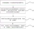
图1是本申请的一实施例的一种显示面板的制作方法的流程示意图;FIG. 1 is a schematic flowchart of a manufacturing method of a display panel according to an embodiment of the present application;
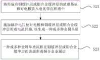
图2是本申请图1的流程图中步骤S2的过程流程示意图;Fig. 2 is the process flow schematic diagram of step S2 in the flow chart of Fig. 1 of the present application;
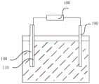
图3是本申请的一实施例电化学沉积装置示意图;3 is a schematic diagram of an electrochemical deposition apparatus according to an embodiment of the present application;
图4是本申请图1的流程图中步骤S2另一实施例的过程流程示意图;4 is a schematic process flow diagram of another embodiment of step S2 in the flowchart of FIG. 1 of the present application;
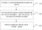
图5是本申请的一实施例的一种显示面板的第二金属层的制作方法流程示意图;5 is a schematic flowchart of a method for fabricating a second metal layer of a display panel according to an embodiment of the present application;
图6是本申请的另一实施例的一种显示面板的制作方法流程示意图;FIG. 6 is a schematic flowchart of a manufacturing method of a display panel according to another embodiment of the present application;
图7是本申请的一实施例的一种显示面板的阵列基板的结构示意图。FIG. 7 is a schematic structural diagram of an array substrate of a display panel according to an embodiment of the present application.
其中,100、玻璃基板;110、缓冲层;120、栅极;130、绝缘层;140、有源层;150、源极;160、漏极;170、铜合金金属层;180、脉冲电源;190、对电极。100, glass substrate; 110, buffer layer; 120, gate electrode; 130, insulating layer; 140, active layer; 150, source electrode; 160, drain electrode; 170, copper alloy metal layer; 180, pulse power supply; 190. Counter electrode.
具体实施方式Detailed ways
需要理解的是,这里所使用的术语、公开的具体结构和功能细节,仅仅是为了描述具体实施例,是代表性的,但是本申请可以通过许多替换形式来具体实现,不应被解释成仅受限于这里所阐述的实施例。It should be understood that the terminology used herein, the specific structural and functional details disclosed are only for describing specific embodiments and are representative, but the present application may be embodied in many alternative forms and should not be construed as only Limited by the embodiments set forth herein.
在本申请的描述中,术语“第一”、“第二”仅用于描述目的,而不能理解为指示相对重要性,或者隐含指明所指示的技术特征的数量。由此,除非另有说明,限定有“第一”、“第二”的特征可以明示或者隐含地包括一个或者更多个该特征;“多个”的含义是两个或两个以上。术语“包括”及其任何变形,意为不排他的包含,可能存在或添加一个或更多其他特征、整数、步骤、操作、单元、组件和/或其组合。In the description of this application, the terms "first" and "second" are only used for description purposes, and cannot be understood as indicating relative importance, or implicitly indicating the number of indicated technical features. Thus, unless otherwise stated, features defined as "first" and "second" may expressly or implicitly include one or more of the features; "plurality" means two or more. The term "comprising" and any variations thereof mean non-exclusive inclusion, possibly the presence or addition of one or more other features, integers, steps, operations, elements, components, and/or combinations thereof.
另外,“中心”、“横向”、“上”、“下”、“左”、“右”、“竖直”、“水平”、“顶”、“底”、“内”、“外”等指示的方位或位置关系的术语,是基于附图所示的方位或相对位置关系描述的,仅是为了便于描述本申请的简化描述,而不是指示所指的装置或元件必须具有特定的方位、以特定的方位构造和操作,因此不能理解为对本申请的限制。In addition, "center", "horizontal", "top", "bottom", "left", "right", "vertical", "horizontal", "top", "bottom", "inside", "outer" The terms of the orientation or positional relationship indicated by etc. are described based on the orientation or relative positional relationship shown in the drawings, and are only for the convenience of describing the simplified description of the present application, rather than indicating that the referred device or element must have a specific orientation , are constructed and operated in a specific orientation, and therefore should not be construed as limiting the application.
此外,除非另有明确的规定和限定,术语“安装”、“相连”、“连接”应做广义理解,例如可以是固定连接,也可以是可拆卸连接,或一体地连接;可以是机械连接,也可以是电连接;可以是直接相连,也可以通过中间媒介间接相连,或是两个元件内部的连通。对于本领域的普通技术人员而言,可以根据具体情况理解上述术语在本申请中的具体含义。In addition, unless otherwise expressly specified and limited, the terms "installed", "connected" and "connected" should be understood in a broad sense, for example, it may be a fixed connection, a detachable connection, or an integral connection; it may be a mechanical connection , it can also be an electrical connection; it can be a direct connection, an indirect connection through an intermediate medium, or an internal connection between two components. For those of ordinary skill in the art, the specific meanings of the above terms in this application can be understood according to specific situations.
一种显示面板,包括TFT(Thin Film Transistor,薄膜晶体管),薄膜晶体管包括栅极、源极和漏极,显示面板还包括数据线,其中栅极、源漏电极和数据线是由金属构成,常规使用的是Al(铝),Al/Mo(铝/钼),Al/Ti(铝/钛)等组合而成,随着对显示面板的需求越来越高,Cu工艺由于诸多优点已成为下一代TFT的开发趋势和工艺需求。但是在实际的TFT开发过程中,Cu的刻蚀问题一直是影响铜制程的关键因素。A display panel includes a TFT (Thin Film Transistor, thin film transistor), the thin film transistor includes a gate electrode, a source electrode and a drain electrode, and the display panel further includes a data line, wherein the gate electrode, the source-drain electrode and the data line are composed of metal, Al (aluminum), Al/Mo (aluminum/molybdenum), Al/Ti (aluminum/titanium), etc. are conventionally used. With the increasing demand for display panels, the Cu process has become a Development trends and process requirements of next-generation TFTs. However, in the actual TFT development process, the etching problem of Cu has always been a key factor affecting the copper process.
下面参考附图和可选的实施例对本申请作详细说明。The present application will be described in detail below with reference to the accompanying drawings and optional embodiments.
图1是本申请的一实施例的一种显示面板的制作方法的流程示意图,如图1所示,本申请公开了一种显示面板的制作方法,包括形成阵列基板的制程,形成所述阵列基板的制程包括步骤:FIG. 1 is a schematic flowchart of a manufacturing method of a display panel according to an embodiment of the present application. As shown in FIG. 1 , the present application discloses a manufacturing method of a display panel, including a process of forming an array substrate, forming the array The manufacturing process of the substrate includes the steps:
S1:在玻璃基板上形成预设图案的缓冲层;S1: forming a buffer layer with a preset pattern on the glass substrate;
S2:将形成有预设图案的缓冲层的玻璃基板放入电化学沉积装置中,进行电化学沉积,形成与预设图案的缓冲层对应的铜合金金属层,其中,铜合金金属层的位置与预设图案的缓冲层的位置对应;S2: Put the glass substrate on which the buffer layer with the preset pattern is formed into an electrochemical deposition device, and perform electrochemical deposition to form a copper alloy metal layer corresponding to the buffer layer with the preset pattern, wherein the position of the copper alloy metal layer is Corresponds to the position of the buffer layer of the preset pattern;
S3:对铜合金金属层进行加热退火处理,形成包括预设图案的缓冲层和铜合金金属层的第一金属层;以及S3: heating and annealing the copper alloy metal layer to form a first metal layer including a buffer layer with a preset pattern and a copper alloy metal layer; and
S4:在第一金属层上依次形成绝缘层、有源层、第二金属层、钝化层和透明电极层;S4: sequentially forming an insulating layer, an active layer, a second metal layer, a passivation layer and a transparent electrode layer on the first metal layer;
其中,预设图案的形状与第一金属层的图案形状对应。Wherein, the shape of the preset pattern corresponds to the pattern shape of the first metal layer.
相对于在形成第一金属层时需要刻蚀铜的方案来说,本申请通过先在玻璃基板上形成与第一金属层对应的预设图案的缓冲层,然后将形成有预设图案的缓冲层放入电化学沉积装置中,沉积铜合金金属层,经过加热退火处理形成预设图案的铜合金金属层第一金属层。在形成铜合金金属层作为第一金属层时,不需要经过刻蚀工艺,因此节省了刻蚀工艺,因此可以避免因刻蚀工艺带来的良率低和成本高的问题,提升了产品良率以及降低成本。Compared with the solution in which copper needs to be etched when forming the first metal layer, in the present application, a buffer layer with a preset pattern corresponding to the first metal layer is formed on the glass substrate, and then the buffer layer with the preset pattern is formed on the glass substrate. The layer is placed in an electrochemical deposition device, a copper alloy metal layer is deposited, and a first metal layer of a copper alloy metal layer with a preset pattern is formed through heating and annealing treatment. When the copper alloy metal layer is formed as the first metal layer, no etching process is required, so the etching process is saved, so the problems of low yield and high cost caused by the etching process can be avoided, and the product quality is improved. rate and reduce costs.
具体的,当阵列基板上形成的薄膜晶体管(TFT)为底栅型的结构时,第一金属层包括通过电化学沉积同层形成的栅极和扫描线,当然TFT也可以为顶栅型的结构,也适用电化学沉积的方法形成栅极。Specifically, when the thin film transistor (TFT) formed on the array substrate has a bottom gate type structure, the first metal layer includes gate electrodes and scan lines formed by electrochemical deposition of the same layer. Of course, the TFT can also be a top gate type. The structure is also suitable for the formation of the gate electrode by the method of electrochemical deposition.
其中,电化学沉积的技术原理为:电化学沉积是指在外电场作用下电流通过电解质溶液中正负离子的迁移并在电极上发生得失电子的氧化还原反应而形成镀层的技术。Among them, the technical principle of electrochemical deposition is as follows: electrochemical deposition refers to the technology of forming a coating layer under the action of an external electric field through the migration of positive and negative ions in the electrolyte solution and the redox reaction of gaining and losing electrons on the electrode.
具体的,所述在玻璃基板上形成预设图案的缓冲层的步骤中,所述缓冲层包括钼缓冲层或钼合金缓冲层。通过设置钼缓冲层或钼合金缓冲层,这样有利于提高与玻璃基板的附着力,当然,所述缓冲层还可以包括Ti(钛)/MoN(氮化钼)等。Specifically, in the step of forming a buffer layer with a preset pattern on the glass substrate, the buffer layer includes a molybdenum buffer layer or a molybdenum alloy buffer layer. By providing a molybdenum buffer layer or a molybdenum alloy buffer layer, it is beneficial to improve the adhesion with the glass substrate. Of course, the buffer layer may also include Ti (titanium)/MoN (molybdenum nitride) and the like.
图2是本申请图1的流程图中步骤S2的过程流程示意图,图3是本申请的一实施例电化学沉积装置示意图,如图2和如图3所示,在玻璃基板上形成预设图案的缓冲层的步骤S1之后,进行将形成有预设图案的缓冲层的玻璃基板放入电化学沉积装置中,进行电化学沉积,形成与预设图案的缓冲层对应的铜合金金属层的步骤S2,包括子步骤:FIG. 2 is a schematic diagram of the process flow of step S2 in the flowchart of FIG. 1 of the present application, and FIG. 3 is a schematic diagram of an electrochemical deposition apparatus according to an embodiment of the present application. As shown in FIG. 2 and FIG. After the step S1 of the patterned buffer layer, the process of placing the glass substrate on which the buffer layer with the preset pattern is formed is placed into an electrochemical deposition device, and performing electrochemical deposition to form a copper alloy metal layer corresponding to the buffer layer with the preset pattern. Step S2 includes sub-steps:
S21:将形成有预设图案的钼缓冲层或钼合金缓冲层的玻璃基板和对电极放入电化学沉积液中;S21: placing the glass substrate and the counter electrode with the molybdenum buffer layer or molybdenum alloy buffer layer formed with the preset pattern into the electrochemical deposition solution;
S22:施加脉冲电压使对电极和钼缓冲层或钼合金缓冲层形成电流回路,促使电化学沉积液中金属阳离子发生还原反应,生成一种或多种金属单质;以及S22: applying a pulse voltage to form a current loop between the counter electrode and the molybdenum buffer layer or the molybdenum alloy buffer layer, to promote the reduction reaction of metal cations in the electrochemical deposition solution to generate one or more metal elements; and
S23:所述一种或多种金属单质沉积在钼缓冲层或钼合金缓冲层的表面形成与预设图案的缓冲层对应的铜合金金属层;S23: The one or more metal elements are deposited on the surface of the molybdenum buffer layer or the molybdenum alloy buffer layer to form a copper alloy metal layer corresponding to the buffer layer of the preset pattern;
其中,电化学沉积装置包括电化学沉积液、脉冲电源180、连接于所述脉冲电源一端的对电极190,所述脉冲电源190的另一端连接于所述钼缓冲层或钼合金缓冲层。The electrochemical deposition device includes an electrochemical deposition solution, a
通过将形成有含有钼或钼合金的缓冲层的玻璃基板以及提供体系电流的对电极放入电化学沉积液中,施加脉冲电压从而形成整个电流回路。通过施加电压的方式,可以定量控制沉中的金属元素比例,使得形成的不同金属的成分可以得到较精确的控制。其中,对电极作为阳极,含有钼缓冲层或者钼合金缓冲层的玻璃基板作为阴极,电化学沉积液中的金属阳离子在阴极发生还原反应,生成金属单质沉积在玻璃基板表面,电化学性质稳定,形成金属单质也比较稳定。电化学沉积操作的持续时间为1分钟。一般的我们需要的膜层的厚度为3000-4000埃米,电化学沉积操作的持续时间为1分钟形成的厚度比较合适。The entire current loop is formed by placing a glass substrate on which a buffer layer containing molybdenum or molybdenum alloy is formed and a counter electrode for supplying a system current into an electrochemical deposition solution and applying a pulse voltage. By applying voltage, the proportion of metal elements in the sink can be quantitatively controlled, so that the composition of different metals formed can be controlled more precisely. Among them, the counter electrode is used as the anode, the glass substrate containing the molybdenum buffer layer or the molybdenum alloy buffer layer is used as the cathode, the metal cations in the electrochemical deposition solution undergo a reduction reaction at the cathode, and the generated metal element is deposited on the surface of the glass substrate, with stable electrochemical properties. The formation of metal element is also relatively stable. The duration of the electrochemical deposition operation was 1 minute. Generally, the thickness of the film layer we need is 3000-4000 angstroms, and the duration of the electrochemical deposition operation is 1 minute to form a suitable thickness.
所述将形成有预设图案的缓冲层的玻璃基板放入电化学沉积装置中,进行电化学沉积,形成与预设图案的缓冲层对应的铜合金金属层,所述电化学沉积液中包括二价铜离子和铬酸根离子。通过控制电化学沉积液中二价铜离子(Cu2+)和铬酸根离子(CrO42-)的浓度,从而使得形成的铜-铬合金结合强度更好。The glass substrate with the buffer layer formed with the preset pattern is put into an electrochemical deposition device, and electrochemical deposition is performed to form a copper alloy metal layer corresponding to the buffer layer with the preset pattern, and the electrochemical deposition solution includes: Divalent copper ions and chromate ions. By controlling the concentration of divalent copper ions (Cu2+) and chromate ions (CrO42- ) in the electrochemical deposition solution, the formed copper-chromium alloy has better bonding strength.
其中,在所述施加脉冲电压使对电极和钼缓冲层或钼合金缓冲层形成电流回路,促使电化学沉积液中金属阳离子发生还原反应,生成一种或多种金属单质的步骤包括子步骤:Wherein, in the described applying pulse voltage, the counter electrode and the molybdenum buffer layer or the molybdenum alloy buffer layer form a current loop to promote the reduction reaction of metal cations in the electrochemical deposition solution, and the step of generating one or more metal elements includes sub-steps:
施加电位为0.3419V的脉冲电压40秒至80秒,使对电极和钼缓冲层或钼合金缓冲层形成电流回路,促使电化学沉积液中二价铜离子发生还原反应,生成铜单质;以及Applying a pulse voltage with a potential of 0.3419V for 40 seconds to 80 seconds makes the counter electrode and the molybdenum buffer layer or the molybdenum alloy buffer layer form a current loop to promote the reduction reaction of divalent copper ions in the electrochemical deposition solution to generate copper element; and
之后施加电位为-0.740V的脉冲电压5秒至10秒,使对电极和钼缓冲层或钼合金缓冲层形成电流回路,促使电化学沉积液中铬酸根发生还原反应,生成铬单质,以获得铜合金金属层。Then apply a pulse voltage of -0.740V for 5 seconds to 10 seconds, so that the counter electrode and the molybdenum buffer layer or the molybdenum alloy buffer layer form a current loop, which promotes the reduction reaction of chromate in the electrochemical deposition solution to generate chromium element to obtain Copper alloy metal layer.
对于控制沉积的合金成分通过调节电压来实现控制的方案来说,由于cu和cr的还原电位电位不一样,通过施加不同的还原电位以及控制施加对应不同电位的持续时间,进行控制沉积的速率,从而可以较精确的控制合金成分沉积的量,有利于提升形成的合金的性能。而且通过电压进行控制的方式,操作简单,容易控制。For the scheme of controlling the deposited alloy composition by adjusting the voltage, since the reduction potentials of cu and cr are different, the deposition rate is controlled by applying different reduction potentials and controlling the duration of the application of the corresponding different potentials. Therefore, the deposition amount of alloy components can be controlled more precisely, which is beneficial to improve the performance of the formed alloy. Moreover, the method of controlling by voltage is simple to operate and easy to control.
其中,Cu2+和CrO42-对应的还原表达式为:Cu2++2e=Cu;CrO42-+4H2O+6e→Cr+8OH-。铜金属离子的还原电位为0.3419V,铬金属离子的还原电位为-0.740V。比如CrO42-还原为Cr3+的电位是-0.740V,在较小的电位下,Cu2+是无法被还原的,只能还原Cr3+,我们可以通过控制电化学沉积液中各离子浓度和电位结合的方法进行控制,比如开始在较高的电位下(即大于0.3419V),电解液中有Cu2+,没有CrO42-或者量很少,只能进行Cu2+的还原沉积,在较低电位下(-0.740V到0.3419V),只能进行CrO42-的还原,这时在电解液中添加一定浓度的CrO42-进行合金离子的沉积。The reduction expressions corresponding to Cu2+ and CrO42- are: Cu2+ +2e=Cu; CrO42- +4H2 O+6e→Cr+8OH-. The reduction potential of copper metal ions is 0.3419V, and the reduction potential of chromium metal ions is -0.740V. For example, the potential of CrO42- to be reduced to Cr3+ is -0.740V. At a lower potential, Cu2+ cannot be reduced, only Cr3+ can be reduced. We can control the concentration of ions in the electrochemical deposition solution and the combination of potential. The method is controlled, such as starting at a higher potential (ie greater than 0.3419V), there is Cu2+ in the electrolyte, no CrO42- or a small amount, only the reduction deposition of Cu2+ can be carried out, at a lower potential (- 0.740V to 0.3419V), only the reduction of CrO42- can be performed. At this time, a certain concentration of CrO42- is added to the electrolyte to deposit alloy ions.
控制合金成分的沉积量可以通过调节脉冲电压的方式控制,还可以通过控制浓度的方式实现控制。图4是本申请图1的流程图中步骤S2另一实施例的过程流程示意图,如图4所示,具体的,所述将形成有预设图案的缓冲层的玻璃基板放入电化学沉积装置中,进行电化学沉积,形成与预设图案的缓冲层对应的铜合金金属层的步骤S2包括子步骤:The deposition amount of the alloy composition can be controlled by adjusting the pulse voltage, and it can also be controlled by controlling the concentration. FIG. 4 is a schematic process flow diagram of another embodiment of step S2 in the flowchart of FIG. 1 of the present application. As shown in FIG. 4 , specifically, the glass substrate with the buffer layer formed with the preset pattern is placed in the electrochemical deposition process. In the device, electrochemical deposition is performed, and the step S2 of forming a copper alloy metal layer corresponding to the buffer layer of the preset pattern includes sub-steps:
S21:将形成有预设图案的钼缓冲层或钼合金缓冲层的玻璃基板放入含有二价铜离子的电化学沉积液中,沉积30秒至100秒,生成铜金属单质;以及S21: placing the glass substrate on which the molybdenum buffer layer or the molybdenum alloy buffer layer with the preset pattern is formed into an electrochemical deposition solution containing divalent copper ions, and depositing for 30 seconds to 100 seconds to generate copper metal element; and
S22:放入含有铬酸根离子的电化学沉积液中,沉积5秒至30秒,生成铬金属单质,以形成铜合金金属层。S22: put into an electrochemical deposition solution containing chromate ions, and deposit for 5 seconds to 30 seconds to generate chromium metal element to form a copper alloy metal layer.
通过单独放入不同的电化学沉积中,即不同的电化学沉积液中含有不同的离子,且浓度都相对于比较高,通过控制电化学沉积液的浓度,从而得到不同占比的合金成分,有利于有利于提升形成的合金的性能。By putting them into different electrochemical depositions separately, that is, different electrochemical deposition solutions contain different ions, and the concentrations are relatively high. It is beneficial to improve the properties of the formed alloy.
以含有Cu2+的电化学沉积液为例,具体的组成成分以及对应的浓度范围为:Cu2+,例如硫酸铜,硝酸铜,氯化铜等,浓度范围为120-250g/L,酸,例如硫酸、盐酸、磷酸等,浓度范围为30-100g/L,光亮剂,例如十二醇硫酸醋钠,聚氧乙烯类,丙烯磺酸钠等,浓度范围为0.3-1ml/L,氯离子,例如氯化钠、氯化钾、氯化镁等,浓度范围为30-120mg/L,整平剂,例如聚苯乙烯,聚丙烯酸,聚乙烯醇等,浓度范围为0.1-0.8ml/L,还包括其他添加剂,例如润湿、开杠剂等,浓度范围为0.1-1.5ml/L。Taking the electrochemical deposition solution containing Cu2+ as an example, the specific composition and the corresponding concentration range are: Cu2+ , such as copper sulfate, copper nitrate, copper chloride, etc., the concentration range is 120-250g/L, acid , such as sulfuric acid, hydrochloric acid, phosphoric acid, etc., the concentration range is 30-100g/L, brighteners, such as sodium dodecyl sulfate, polyoxyethylene, sodium propylene sulfonate, etc., the concentration range is 0.3-1ml/L, chlorine Ions, such as sodium chloride, potassium chloride, magnesium chloride, etc., with a concentration range of 30-120mg/L, leveling agents, such as polystyrene, polyacrylic acid, polyvinyl alcohol, etc., with a concentration range of 0.1-0.8ml/L, Other additives are also included, such as wetting agents, openers, etc., in a concentration range of 0.1-1.5ml/L.
在将形成有预设图案的缓冲层的玻璃基板放入电化学沉积装置中,进行电化学沉积,形成与预设图案的缓冲层对应的铜合金金属层的步骤之后,进行对铜合金金属层进行加热退火处理形成包括预设图案的缓冲层和铜合金金属层的第一金属层的步骤,具体包括子步骤:After the step of placing the glass substrate on which the buffer layer with the preset pattern is formed into an electrochemical deposition device, performing electrochemical deposition, and forming the copper alloy metal layer corresponding to the buffer layer with the preset pattern, the copper alloy metal layer is deposited on the glass substrate. The step of forming a first metal layer including a buffer layer with a preset pattern and a copper alloy metal layer by thermal annealing treatment specifically includes sub-steps:
对铜合金金属层进行加热,加热温度为300摄氏度至500摄氏度,加热时间为30分钟至120分钟,使得铬扩散到表面,形成位于铜合金金属层表面的钝化保护层。The copper alloy metal layer is heated, the heating temperature is 300 degrees Celsius to 500 degrees Celsius, and the heating time is 30 minutes to 120 minutes, so that the chromium diffuses to the surface and forms a passivation protection layer on the surface of the copper alloy metal layer.
在加热退火的过程中,退火可以将沉积Cu和Cr原子晶格重排,形成我们需要的晶格结构,另外利用合金的自扩散性,温度不同,扩散系数不同,其中,铬的热扩散系数相对较大,使得铬扩散到表面,形成一层钝化保护层,形成的钝化层保护层可以对Cu起到保护作用,阻止Cu向其他层扩散,从而提高器件性能。In the process of thermal annealing, annealing can rearrange the crystal lattices of the deposited Cu and Cr atoms to form the lattice structure we need. In addition, the self-diffusivity of the alloy is used. The temperature is different and the diffusivity is different. Among them, the thermal diffusivity of chromium is different. It is relatively large, so that chromium diffuses to the surface to form a passivation protective layer, and the formed passivation layer protective layer can protect Cu and prevent Cu from diffusing to other layers, thereby improving device performance.
图5是本申请的一实施例的一种显示面板的第二金属层的制作方法流程示意图,如图5所示,所述在第一金属层上依次形成绝缘层、有源层、第二金属层、钝化层和透明电极层以形成阵列基板的步骤S4中,其中形成第二金属层的步骤包括:5 is a schematic flowchart of a method for fabricating a second metal layer of a display panel according to an embodiment of the present application. As shown in FIG. 5 , an insulating layer, an active layer, and a second metal layer are sequentially formed on the first metal layer. In the step S4 of forming the array substrate with the metal layer, the passivation layer and the transparent electrode layer, the step of forming the second metal layer includes:
S41:在有源层上沉积预设图案的钼缓冲层或钼合金缓冲层;S41: depositing a molybdenum buffer layer or a molybdenum alloy buffer layer with a preset pattern on the active layer;
S42:将形成有预设图案的钼缓冲层或钼合金缓冲层的玻璃基板放入电化学沉积装置中,进行电化学沉积,形成与预设图案的缓冲层对应的铜合金金属层;以及S42: placing the glass substrate on which the molybdenum buffer layer or the molybdenum alloy buffer layer with the preset pattern is formed into an electrochemical deposition device, and performing electrochemical deposition to form a copper alloy metal layer corresponding to the buffer layer with the preset pattern; and
S43:对铜合金金属层进行加热退火处理形成包括预设图案的缓冲层和铜合金金属层的第二金属层。S43: Perform heat annealing treatment on the copper alloy metal layer to form a second metal layer including a buffer layer with a preset pattern and a copper alloy metal layer.
通过先在有源层上形成与第一金属层对应的预设图案的缓冲层,然后将形成有预设图案的缓冲层放入电化学沉积装置中,沉积铜合金金属层,经过加热退火处理形成预设图案的铜合金金属层第二金属层。在形成铜合金金属层作为第二金属层时,不需要经过刻蚀工艺,因此节省了刻蚀工艺,因此可以避免因刻蚀工艺带来的良率低和成本高的问题,提升了产品良率以及降低成本。另外缓冲层包括钼金属缓冲层和钼合金缓冲层可以提升附着力。First, a buffer layer with a preset pattern corresponding to the first metal layer is formed on the active layer, and then the buffer layer with the preset pattern is placed in an electrochemical deposition device to deposit a copper alloy metal layer, and then heat and anneal. A second metal layer of a copper alloy metal layer of a preset pattern is formed. When the copper alloy metal layer is formed as the second metal layer, no etching process is required, so the etching process is saved, so the problems of low yield and high cost caused by the etching process can be avoided, and the product quality is improved. rate and reduce costs. In addition, the buffer layer includes a molybdenum metal buffer layer and a molybdenum alloy buffer layer to improve adhesion.
图6是本申请的另一实施例的一种显示面板的制作方法流程示意图,如图6所示,作为本申请的另一实施例,本申请还公开了一种显示面板的制作方法,包括形成阵列基板的制程,形成所述阵列基板的制程包括步骤:FIG. 6 is a schematic flowchart of a method for manufacturing a display panel according to another embodiment of the present application. As shown in FIG. 6 , as another embodiment of the present application, the present application further discloses a method for manufacturing a display panel, including: The process of forming the array substrate, the process of forming the array substrate includes the steps:
S1:在玻璃基板上形成预设图案的钼缓冲层或钼合金缓冲层;S1: forming a molybdenum buffer layer or a molybdenum alloy buffer layer with a preset pattern on the glass substrate;
S21:将形成有预设图案的钼缓冲层或钼合金缓冲层的玻璃基板,以及共同形成电流回路的对电极,放入含有铜金属离子和铬金属离子的电化学沉积液中;通过短路条,由扫描线施加脉冲电压,使对电极和钼缓冲层或钼合金缓冲层形成电流回路;S21: Put the glass substrate on which the molybdenum buffer layer or the molybdenum alloy buffer layer with the preset pattern is formed, and the counter electrode which together form the current loop, into the electrochemical deposition solution containing copper metal ions and chromium metal ions; , the pulse voltage is applied by the scanning line, so that the counter electrode and the molybdenum buffer layer or the molybdenum alloy buffer layer form a current loop;
S22:施加电位为0.3419V的脉冲电压40秒至80秒,使对电极和钼缓冲层或钼合金缓冲层形成电流回路,促使电化学沉积液中二价铜离子发生还原反应,生成铜单质;然后施加电位为-0.740V的脉冲电压5秒至10秒,使对电极和钼缓冲层或钼合金缓冲层形成电流回路,促使电化学沉积液中铬酸根发生还原反应,生成铬单质,以获得铜合金金属层;S22: Apply a pulse voltage with a potential of 0.3419V for 40 seconds to 80 seconds to form a current loop between the counter electrode and the molybdenum buffer layer or the molybdenum alloy buffer layer, and promote the reduction reaction of divalent copper ions in the electrochemical deposition solution to generate copper element; Then, a pulse voltage of -0.740V is applied for 5 seconds to 10 seconds, so that the counter electrode and the molybdenum buffer layer or the molybdenum alloy buffer layer form a current loop, which promotes the reduction reaction of chromate in the electrochemical deposition solution to generate chromium element, so as to obtain Copper alloy metal layer;
S3:对铜合金金属层进行加热,加热温度为300摄氏度至500摄氏度,加热时间为30分钟至120分钟,使得铬扩散到表面,形成位于铜合金金属层表面的钝化保护层,形成的预设图案的缓冲层和铜合金金属层作为栅极金属层和/或扫描线金属层;以及S3: Heating the copper alloy metal layer, the heating temperature is 300 degrees Celsius to 500 degrees Celsius, and the heating time is 30 minutes to 120 minutes, so that the chromium diffuses to the surface, and the passivation protection layer on the surface of the copper alloy metal layer is formed. patterned buffer layers and copper alloy metal layers as gate metal layers and/or scan line metal layers; and
S4:在栅极金属层和/或扫描线金属层上依次形成绝缘层、有源层、源漏极金属层和/或数据线金属层、钝化层和透明电极层以形成阵列基板。S4: sequentially forming an insulating layer, an active layer, a source-drain metal layer and/or a data line metal layer, a passivation layer and a transparent electrode layer on the gate metal layer and/or the scan line metal layer to form an array substrate.
本申请通过先在玻璃基板上形成与第一金属层对应的预设图案的缓冲层,然后将形成有预设图案的缓冲层放入电化学沉积装置中,沉积铜合金金属层,经过加热退火处理形成预设图案的铜合金金属层第一金属层。在形成铜合金金属层作为第一金属层时,不需要经过刻蚀工艺,因此节省了刻蚀工艺,因此可以避免因刻蚀工艺带来的良率低和成本高的问题,提升了产品良率以及降低成本。在热退火的过程中,利用合金的自扩散性,温度不同,扩散系数不同,形成一层钝化保护层,形成的钝化层保护层可以对Cu起到保护作用,阻止Cu向其他层扩散,从而提高器件性能。采用电化学沉积工艺,在常温液相中制备,避免因形成粗大的颗粒而导致表面平整度差引起电导率下降的问题。In the present application, a buffer layer with a preset pattern corresponding to the first metal layer is first formed on a glass substrate, and then the buffer layer with the preset pattern is placed in an electrochemical deposition device to deposit a copper alloy metal layer, and then heat and anneal. The first metal layer of the copper alloy metal layer formed in the preset pattern is processed. When the copper alloy metal layer is formed as the first metal layer, no etching process is required, so the etching process is saved, so the problems of low yield and high cost caused by the etching process can be avoided, and the product quality is improved. rate and reduce costs. In the process of thermal annealing, a passivation protective layer is formed by using the self-diffusivity of the alloy, the temperature is different, and the diffusion coefficient is different. The formed passivation layer protective layer can protect Cu and prevent Cu from diffusing to other layers. , thereby improving device performance. Electrochemical deposition process is adopted, and it is prepared in liquid phase at room temperature to avoid the problem of conductivity drop caused by poor surface flatness due to the formation of coarse particles.
图7是本申请的一实施例的一种显示面板的结构示意图,如图7所示,本申请还公开了一种显示面板,采用上述的显示面板的制作方法制成的阵列基板,以及与所述阵列基板相对设置的彩膜基板。所述阵列基板包括玻璃基板100、缓冲层110、栅极120、绝缘层130、有源层140、源极150、漏极160、钝化层和透明电极层,所述缓冲层设置在所述玻璃基板上;所述栅极设置在所述缓冲层上;所述绝缘层覆盖所述栅极;所述有源层设置在所述绝缘层上;所述源极和漏极设置在所述有源层的两侧;在源极和漏极上依次形成钝化层和透明电极层。FIG. 7 is a schematic structural diagram of a display panel according to an embodiment of the present application. As shown in FIG. 7 , the present application also discloses a display panel, an array substrate manufactured by the above-mentioned manufacturing method of the display panel, and The array substrate is opposite to the color filter substrate. The array substrate includes a
需要说明的是,本方案中涉及到的各步骤的限定,在不影响具体方案实施的前提下,并不认定为对步骤先后顺序做出限定,写在前面的步骤可以是在先执行的,也可以是在后执行的,甚至也可以是同时执行的,只要能实施本方案,都应当视为属于本申请的保护范围。It should be noted that the limitations of the steps involved in this scheme are not considered to limit the sequence of steps without affecting the implementation of the specific scheme. The steps written in the front may be executed first. It can also be executed later, or even executed at the same time, as long as the solution can be implemented, it should be regarded as belonging to the protection scope of the present application.
本申请的技术方案可以广泛用于各种显示面板,如TN(Twisted Nematic,扭曲向列型)显示面板、IPS(In-Plane Switching,平面转换型)显示面板、VA(VerticalAlignment,垂直配向型)显示面板、MVA(Multi-Domain Vertical Alignment,多象限垂直配向型)显示面板,当然,也可以是其他类型的显示面板,如OLED(Organic Light-EmittingDiode,有机发光二极管)显示面板,均可适用上述方案。The technical solution of the present application can be widely used in various display panels, such as TN (Twisted Nematic, twisted nematic) display panels, IPS (In-Plane Switching, in-plane switching) display panels, VA (Vertical Alignment, vertical alignment type) Display panel, MVA (Multi-Domain Vertical Alignment, multi-quadrant vertical alignment type) display panel, of course, can also be other types of display panels, such as OLED (Organic Light-Emitting Diode, organic light-emitting diode) display panels, all of which are applicable to the above Program.
以上内容是结合具体的可选实施方式对本申请所作的进一步详细说明,不能认定本申请的具体实施只局限于这些说明。对于本申请所属技术领域的普通技术人员来说,在不脱离本申请构思的前提下,还可以做出若干简单推演或替换,都应当视为属于本申请的保护范围。The above content is a further detailed description of the present application in conjunction with specific optional embodiments, and it cannot be considered that the specific implementation of the present application is limited to these descriptions. For those of ordinary skill in the technical field of the present application, without departing from the concept of the present application, some simple deductions or substitutions can be made, which should be regarded as belonging to the protection scope of the present application.
Claims (10)
Translated fromChinesePriority Applications (2)
| Application Number | Priority Date | Filing Date | Title |
|---|---|---|---|
| CN202010743740.XACN111900175A (en) | 2020-07-29 | 2020-07-29 | Display panel and manufacturing method thereof |
| US17/377,399US11791349B2 (en) | 2020-07-29 | 2021-07-16 | Manufacturing method for display panel and display panel |
Applications Claiming Priority (1)
| Application Number | Priority Date | Filing Date | Title |
|---|---|---|---|
| CN202010743740.XACN111900175A (en) | 2020-07-29 | 2020-07-29 | Display panel and manufacturing method thereof |
Publications (1)
| Publication Number | Publication Date |
|---|---|
| CN111900175Atrue CN111900175A (en) | 2020-11-06 |
Family
ID=73182417
Family Applications (1)
| Application Number | Title | Priority Date | Filing Date |
|---|---|---|---|
| CN202010743740.XAPendingCN111900175A (en) | 2020-07-29 | 2020-07-29 | Display panel and manufacturing method thereof |
Country Status (2)
| Country | Link |
|---|---|
| US (1) | US11791349B2 (en) |
| CN (1) | CN111900175A (en) |
Citations (5)
| Publication number | Priority date | Publication date | Assignee | Title |
|---|---|---|---|---|
| US4586988A (en)* | 1983-08-19 | 1986-05-06 | Energy Conversion Devices, Inc. | Method of forming an electrically conductive member |
| WO2002045142A2 (en)* | 2000-11-15 | 2002-06-06 | Intel Corporation | Copper alloy interconnections for integrated circuits and methods of making same |
| US20040203181A1 (en)* | 2003-04-11 | 2004-10-14 | Quanyuan Shang | Methods to form metal lines using selective electrochemical deposition |
| CN104701384A (en)* | 2015-04-09 | 2015-06-10 | 京东方科技集团股份有限公司 | Thin film transistor, preparation method thereof, array substrate and display device |
| US20190196285A1 (en)* | 2017-12-26 | 2019-06-27 | Shenzhen China Star Optoelectronics Semiconductor Display Technology Co., Ltd. | Manufacturing method of array substrate and its upper electrode line pattern and liquid crystal display panel |
Family Cites Families (1)
| Publication number | Priority date | Publication date | Assignee | Title |
|---|---|---|---|---|
| KR100870697B1 (en)* | 2002-03-07 | 2008-11-27 | 엘지디스플레이 주식회사 | Method for fabricating of low resistivity Copper |
- 2020
- 2020-07-29CNCN202010743740.XApatent/CN111900175A/enactivePending
- 2021
- 2021-07-16USUS17/377,399patent/US11791349B2/enactiveActive
Patent Citations (5)
| Publication number | Priority date | Publication date | Assignee | Title |
|---|---|---|---|---|
| US4586988A (en)* | 1983-08-19 | 1986-05-06 | Energy Conversion Devices, Inc. | Method of forming an electrically conductive member |
| WO2002045142A2 (en)* | 2000-11-15 | 2002-06-06 | Intel Corporation | Copper alloy interconnections for integrated circuits and methods of making same |
| US20040203181A1 (en)* | 2003-04-11 | 2004-10-14 | Quanyuan Shang | Methods to form metal lines using selective electrochemical deposition |
| CN104701384A (en)* | 2015-04-09 | 2015-06-10 | 京东方科技集团股份有限公司 | Thin film transistor, preparation method thereof, array substrate and display device |
| US20190196285A1 (en)* | 2017-12-26 | 2019-06-27 | Shenzhen China Star Optoelectronics Semiconductor Display Technology Co., Ltd. | Manufacturing method of array substrate and its upper electrode line pattern and liquid crystal display panel |
Non-Patent Citations (1)
| Title |
|---|
| 王运赣: "《快速模具制造及其应用》", 30 September 2003* |
Also Published As
| Publication number | Publication date |
|---|---|
| US11791349B2 (en) | 2023-10-17 |
| US20220037371A1 (en) | 2022-02-03 |
Similar Documents
| Publication | Publication Date | Title |
|---|---|---|
| JP3410667B2 (en) | Reflective liquid crystal display device and method of manufacturing the same | |
| CN105374748A (en) | Preparing method of film transistor substrate and prepared film transistor substrate | |
| CN104250814B (en) | Etching agent composite | |
| CN103700665A (en) | Metal oxide thin film transistor array substrate, manufacturing method thereof, and display device | |
| CN102522429A (en) | Thin film transistor on basis of metal oxide and preparation method and application thereof | |
| CN102332404A (en) | Preparation method of thin film transistor based on anodized insulating layer | |
| CN107452758B (en) | Display substrate, method for manufacturing the same, and display device | |
| US20160343744A1 (en) | Liquid Crystal Display Panel, Array Substrate And Manufacturing Method For Thin-Film Transistor | |
| CN102623510A (en) | Thin film transistor based on tantalum oxide insulating layer and preparation method thereof | |
| CN111900175A (en) | Display panel and manufacturing method thereof | |
| US10325935B2 (en) | Display panel, production method of the same, and display apparatus | |
| WO2014056252A1 (en) | Thin film transistor active device and manufacturing method thereof | |
| US11515342B2 (en) | Gate unit and manufacturing method thereof, array substrate manufacturing method, and display mechanism | |
| US20190280012A1 (en) | Conductive pattern structure, manufacturing method thereof, array substrate and display device | |
| TWI608077B (en) | Etchant composition for forming a wiring and a reflection layer of silver or silver alloy | |
| CN109461660A (en) | A kind of metal-oxide film and preparation method thereof, thin film transistor (TFT) and array substrate | |
| CN112002698B (en) | Preparation method of data line, preparation method of array substrate and display mechanism | |
| US11244964B2 (en) | Display device, array substrate and manufacturing method thereof | |
| WO2019100487A1 (en) | Back channel etching type tft substrate and method for manufacturing same | |
| US11830887B2 (en) | Array substrate, manufacturing method of the array substrate, and display panel | |
| CN103236403B (en) | Barrier layer and preparation method, thin-film transistor, array base palte, display unit | |
| CN112114460B (en) | Insulation unit based on array substrate and its preparation method, array substrate and its preparation method, display mechanism | |
| WO2020172920A1 (en) | Method for manufacturing tft substrate and tft substrate | |
| JPH11186558A (en) | Thin film transistor and method of manufacturing the same | |
| WO2023240715A1 (en) | Display panel, display apparatus, and manufacturing method |
Legal Events
| Date | Code | Title | Description |
|---|---|---|---|
| PB01 | Publication | ||
| PB01 | Publication | ||
| SE01 | Entry into force of request for substantive examination | ||
| SE01 | Entry into force of request for substantive examination | ||
| RJ01 | Rejection of invention patent application after publication | Application publication date:20201106 | |
| RJ01 | Rejection of invention patent application after publication |