CN111900134A - Power semiconductor module device and method of manufacturing the same - Google Patents
Power semiconductor module device and method of manufacturing the sameDownload PDFInfo
- Publication number
- CN111900134A CN111900134ACN202010362239.9ACN202010362239ACN111900134ACN 111900134 ACN111900134 ACN 111900134ACN 202010362239 ACN202010362239 ACN 202010362239ACN 111900134 ACN111900134 ACN 111900134A
- Authority
- CN
- China
- Prior art keywords
- frame
- terminal element
- housing
- terminal
- semiconductor substrate
- Prior art date
- Legal status (The legal status is an assumption and is not a legal conclusion. Google has not performed a legal analysis and makes no representation as to the accuracy of the status listed.)
- Pending
Links
Images


Classifications
- H—ELECTRICITY
- H01—ELECTRIC ELEMENTS
- H01L—SEMICONDUCTOR DEVICES NOT COVERED BY CLASS H10
- H01L23/00—Details of semiconductor or other solid state devices
- H01L23/02—Containers; Seals
- H01L23/04—Containers; Seals characterised by the shape of the container or parts, e.g. caps, walls
- H01L23/043—Containers; Seals characterised by the shape of the container or parts, e.g. caps, walls the container being a hollow construction and having a conductive base as a mounting as well as a lead for the semiconductor body
- H01L23/049—Containers; Seals characterised by the shape of the container or parts, e.g. caps, walls the container being a hollow construction and having a conductive base as a mounting as well as a lead for the semiconductor body the other leads being perpendicular to the base
- H—ELECTRICITY
- H01—ELECTRIC ELEMENTS
- H01L—SEMICONDUCTOR DEVICES NOT COVERED BY CLASS H10
- H01L23/00—Details of semiconductor or other solid state devices
- H01L23/02—Containers; Seals
- H01L23/04—Containers; Seals characterised by the shape of the container or parts, e.g. caps, walls
- H01L23/053—Containers; Seals characterised by the shape of the container or parts, e.g. caps, walls the container being a hollow construction and having an insulating or insulated base as a mounting for the semiconductor body
- H01L23/057—Containers; Seals characterised by the shape of the container or parts, e.g. caps, walls the container being a hollow construction and having an insulating or insulated base as a mounting for the semiconductor body the leads being parallel to the base
- H—ELECTRICITY
- H01—ELECTRIC ELEMENTS
- H01L—SEMICONDUCTOR DEVICES NOT COVERED BY CLASS H10
- H01L21/00—Processes or apparatus adapted for the manufacture or treatment of semiconductor or solid state devices or of parts thereof
- H01L21/02—Manufacture or treatment of semiconductor devices or of parts thereof
- H01L21/04—Manufacture or treatment of semiconductor devices or of parts thereof the devices having potential barriers, e.g. a PN junction, depletion layer or carrier concentration layer
- H01L21/48—Manufacture or treatment of parts, e.g. containers, prior to assembly of the devices, using processes not provided for in a single one of the groups H01L21/18 - H01L21/326 or H10D48/04 - H10D48/07
- H01L21/4814—Conductive parts
- H01L21/4817—Conductive parts for containers, e.g. caps
- H—ELECTRICITY
- H01—ELECTRIC ELEMENTS
- H01L—SEMICONDUCTOR DEVICES NOT COVERED BY CLASS H10
- H01L23/00—Details of semiconductor or other solid state devices
- H01L23/02—Containers; Seals
- H01L23/04—Containers; Seals characterised by the shape of the container or parts, e.g. caps, walls
- H01L23/053—Containers; Seals characterised by the shape of the container or parts, e.g. caps, walls the container being a hollow construction and having an insulating or insulated base as a mounting for the semiconductor body
- H—ELECTRICITY
- H01—ELECTRIC ELEMENTS
- H01L—SEMICONDUCTOR DEVICES NOT COVERED BY CLASS H10
- H01L23/00—Details of semiconductor or other solid state devices
- H01L23/12—Mountings, e.g. non-detachable insulating substrates
- H01L23/14—Mountings, e.g. non-detachable insulating substrates characterised by the material or its electrical properties
- H—ELECTRICITY
- H01—ELECTRIC ELEMENTS
- H01L—SEMICONDUCTOR DEVICES NOT COVERED BY CLASS H10
- H01L23/00—Details of semiconductor or other solid state devices
- H01L23/16—Fillings or auxiliary members in containers or encapsulations, e.g. centering rings
- H01L23/18—Fillings characterised by the material, its physical or chemical properties, or its arrangement within the complete device
- H—ELECTRICITY
- H01—ELECTRIC ELEMENTS
- H01L—SEMICONDUCTOR DEVICES NOT COVERED BY CLASS H10
- H01L23/00—Details of semiconductor or other solid state devices
- H01L23/48—Arrangements for conducting electric current to or from the solid state body in operation, e.g. leads, terminal arrangements ; Selection of materials therefor
- H01L23/488—Arrangements for conducting electric current to or from the solid state body in operation, e.g. leads, terminal arrangements ; Selection of materials therefor consisting of soldered or bonded constructions
- H01L23/498—Leads, i.e. metallisations or lead-frames on insulating substrates, e.g. chip carriers
- H01L23/49811—Additional leads joined to the metallisation on the insulating substrate, e.g. pins, bumps, wires, flat leads
- H—ELECTRICITY
- H01—ELECTRIC ELEMENTS
- H01L—SEMICONDUCTOR DEVICES NOT COVERED BY CLASS H10
- H01L24/00—Arrangements for connecting or disconnecting semiconductor or solid-state bodies; Methods or apparatus related thereto
- H01L24/01—Means for bonding being attached to, or being formed on, the surface to be connected, e.g. chip-to-package, die-attach, "first-level" interconnects; Manufacturing methods related thereto
- H01L24/42—Wire connectors; Manufacturing methods related thereto
- H01L24/47—Structure, shape, material or disposition of the wire connectors after the connecting process
- H01L24/48—Structure, shape, material or disposition of the wire connectors after the connecting process of an individual wire connector
- H—ELECTRICITY
- H01—ELECTRIC ELEMENTS
- H01L—SEMICONDUCTOR DEVICES NOT COVERED BY CLASS H10
- H01L25/00—Assemblies consisting of a plurality of semiconductor or other solid state devices
- H01L25/50—Multistep manufacturing processes of assemblies consisting of devices, the devices being individual devices of subclass H10D or integrated devices of class H10
- H—ELECTRICITY
- H01—ELECTRIC ELEMENTS
- H01L—SEMICONDUCTOR DEVICES NOT COVERED BY CLASS H10
- H01L2224/00—Indexing scheme for arrangements for connecting or disconnecting semiconductor or solid-state bodies and methods related thereto as covered by H01L24/00
- H01L2224/01—Means for bonding being attached to, or being formed on, the surface to be connected, e.g. chip-to-package, die-attach, "first-level" interconnects; Manufacturing methods related thereto
- H01L2224/26—Layer connectors, e.g. plate connectors, solder or adhesive layers; Manufacturing methods related thereto
- H01L2224/31—Structure, shape, material or disposition of the layer connectors after the connecting process
- H01L2224/32—Structure, shape, material or disposition of the layer connectors after the connecting process of an individual layer connector
- H01L2224/321—Disposition
- H01L2224/32151—Disposition the layer connector connecting between a semiconductor or solid-state body and an item not being a semiconductor or solid-state body, e.g. chip-to-substrate, chip-to-passive
- H01L2224/32221—Disposition the layer connector connecting between a semiconductor or solid-state body and an item not being a semiconductor or solid-state body, e.g. chip-to-substrate, chip-to-passive the body and the item being stacked
- H01L2224/32225—Disposition the layer connector connecting between a semiconductor or solid-state body and an item not being a semiconductor or solid-state body, e.g. chip-to-substrate, chip-to-passive the body and the item being stacked the item being non-metallic, e.g. insulating substrate with or without metallisation
- H—ELECTRICITY
- H01—ELECTRIC ELEMENTS
- H01L—SEMICONDUCTOR DEVICES NOT COVERED BY CLASS H10
- H01L2224/00—Indexing scheme for arrangements for connecting or disconnecting semiconductor or solid-state bodies and methods related thereto as covered by H01L24/00
- H01L2224/01—Means for bonding being attached to, or being formed on, the surface to be connected, e.g. chip-to-package, die-attach, "first-level" interconnects; Manufacturing methods related thereto
- H01L2224/42—Wire connectors; Manufacturing methods related thereto
- H01L2224/47—Structure, shape, material or disposition of the wire connectors after the connecting process
- H01L2224/48—Structure, shape, material or disposition of the wire connectors after the connecting process of an individual wire connector
- H01L2224/481—Disposition
- H01L2224/48151—Connecting between a semiconductor or solid-state body and an item not being a semiconductor or solid-state body, e.g. chip-to-substrate, chip-to-passive
- H01L2224/48221—Connecting between a semiconductor or solid-state body and an item not being a semiconductor or solid-state body, e.g. chip-to-substrate, chip-to-passive the body and the item being stacked
- H01L2224/48225—Connecting between a semiconductor or solid-state body and an item not being a semiconductor or solid-state body, e.g. chip-to-substrate, chip-to-passive the body and the item being stacked the item being non-metallic, e.g. insulating substrate with or without metallisation
- H01L2224/48227—Connecting between a semiconductor or solid-state body and an item not being a semiconductor or solid-state body, e.g. chip-to-substrate, chip-to-passive the body and the item being stacked the item being non-metallic, e.g. insulating substrate with or without metallisation connecting the wire to a bond pad of the item
- H—ELECTRICITY
- H01—ELECTRIC ELEMENTS
- H01L—SEMICONDUCTOR DEVICES NOT COVERED BY CLASS H10
- H01L2224/00—Indexing scheme for arrangements for connecting or disconnecting semiconductor or solid-state bodies and methods related thereto as covered by H01L24/00
- H01L2224/01—Means for bonding being attached to, or being formed on, the surface to be connected, e.g. chip-to-package, die-attach, "first-level" interconnects; Manufacturing methods related thereto
- H01L2224/42—Wire connectors; Manufacturing methods related thereto
- H01L2224/47—Structure, shape, material or disposition of the wire connectors after the connecting process
- H01L2224/48—Structure, shape, material or disposition of the wire connectors after the connecting process of an individual wire connector
- H01L2224/484—Connecting portions
- H01L2224/4847—Connecting portions the connecting portion on the bonding area of the semiconductor or solid-state body being a wedge bond
- H01L2224/48472—Connecting portions the connecting portion on the bonding area of the semiconductor or solid-state body being a wedge bond the other connecting portion not on the bonding area also being a wedge bond, i.e. wedge-to-wedge
- H—ELECTRICITY
- H01—ELECTRIC ELEMENTS
- H01L—SEMICONDUCTOR DEVICES NOT COVERED BY CLASS H10
- H01L2224/00—Indexing scheme for arrangements for connecting or disconnecting semiconductor or solid-state bodies and methods related thereto as covered by H01L24/00
- H01L2224/73—Means for bonding being of different types provided for in two or more of groups H01L2224/10, H01L2224/18, H01L2224/26, H01L2224/34, H01L2224/42, H01L2224/50, H01L2224/63, H01L2224/71
- H01L2224/732—Location after the connecting process
- H01L2224/73251—Location after the connecting process on different surfaces
- H01L2224/73265—Layer and wire connectors
- H—ELECTRICITY
- H01—ELECTRIC ELEMENTS
- H01L—SEMICONDUCTOR DEVICES NOT COVERED BY CLASS H10
- H01L23/00—Details of semiconductor or other solid state devices
- H01L23/28—Encapsulations, e.g. encapsulating layers, coatings, e.g. for protection
- H—ELECTRICITY
- H01—ELECTRIC ELEMENTS
- H01L—SEMICONDUCTOR DEVICES NOT COVERED BY CLASS H10
- H01L23/00—Details of semiconductor or other solid state devices
- H01L23/34—Arrangements for cooling, heating, ventilating or temperature compensation ; Temperature sensing arrangements
- H01L23/36—Selection of materials, or shaping, to facilitate cooling or heating, e.g. heatsinks
- H01L23/373—Cooling facilitated by selection of materials for the device or materials for thermal expansion adaptation, e.g. carbon
- H01L23/3735—Laminates or multilayers, e.g. direct bond copper ceramic substrates
- H—ELECTRICITY
- H01—ELECTRIC ELEMENTS
- H01L—SEMICONDUCTOR DEVICES NOT COVERED BY CLASS H10
- H01L25/00—Assemblies consisting of a plurality of semiconductor or other solid state devices
- H01L25/03—Assemblies consisting of a plurality of semiconductor or other solid state devices all the devices being of a type provided for in a single subclass of subclasses H10B, H10D, H10F, H10H, H10K or H10N, e.g. assemblies of rectifier diodes
- H01L25/04—Assemblies consisting of a plurality of semiconductor or other solid state devices all the devices being of a type provided for in a single subclass of subclasses H10B, H10D, H10F, H10H, H10K or H10N, e.g. assemblies of rectifier diodes the devices not having separate containers
- H01L25/07—Assemblies consisting of a plurality of semiconductor or other solid state devices all the devices being of a type provided for in a single subclass of subclasses H10B, H10D, H10F, H10H, H10K or H10N, e.g. assemblies of rectifier diodes the devices not having separate containers the devices being of a type provided for in group subclass H10D
- H01L25/072—Assemblies consisting of a plurality of semiconductor or other solid state devices all the devices being of a type provided for in a single subclass of subclasses H10B, H10D, H10F, H10H, H10K or H10N, e.g. assemblies of rectifier diodes the devices not having separate containers the devices being of a type provided for in group subclass H10D the devices being arranged next to each other
Landscapes
- Engineering & Computer Science (AREA)
- Microelectronics & Electronic Packaging (AREA)
- Power Engineering (AREA)
- Computer Hardware Design (AREA)
- Physics & Mathematics (AREA)
- Condensed Matter Physics & Semiconductors (AREA)
- General Physics & Mathematics (AREA)
- Manufacturing & Machinery (AREA)
- Structures Or Materials For Encapsulating Or Coating Semiconductor Devices Or Solid State Devices (AREA)
- Cooling Or The Like Of Semiconductors Or Solid State Devices (AREA)
Abstract
Translated fromChinese
Description
Translated fromChinese技术领域technical field
本公开涉及功率半导体模块装置及其制造方法。The present disclosure relates to a power semiconductor module device and a method of manufacturing the same.
背景技术Background technique
功率半导体模块装置往往包括布置在外壳中的至少一个半导体衬底。包括多个可控半导体元件(例如,半桥构造中的两个IGBT)的半导体装置布置在所述至少一个衬底中的每者上。每一衬底通常包括衬底层(例如,陶瓷层)、沉积在衬底层的第一侧上的第一金属化层、以及沉积在衬底层的第二侧上的第二金属化层。例如,可控半导体元件安装在第一金属化层上。第二金属化层可以任选地附接至基板。可控半导体器件通常通过焊接或烧结技术安装到半导体衬底。Power semiconductor module arrangements often include at least one semiconductor substrate arranged in a housing. A semiconductor device comprising a plurality of controllable semiconductor elements (eg, two IGBTs in a half-bridge configuration) is arranged on each of the at least one substrate. Each substrate typically includes a substrate layer (eg, a ceramic layer), a first metallization layer deposited on a first side of the substrate layer, and a second metallization layer deposited on a second side of the substrate layer. For example, controllable semiconductor elements are mounted on the first metallization layer. A second metallization layer can optionally be attached to the substrate. Controllable semiconductor devices are typically mounted to semiconductor substrates by soldering or sintering techniques.
电线或电连接部用于连接功率半导体装置的不同半导体器件。此外,还提供端子元件,从而从外壳外部接触半导体装置。这样的端子元件通常以第一端电耦合至第一金属化层。端子元件的第二端伸出到外壳外部。例如,通常用包封材料填充外壳,以保护不同元件免遭机械损伤以及免受诸如腐蚀性气体的有害物质的影响。此外,包封材料还在不同元件之间提供介电绝缘。然而,因为内部张力可能由于包封材料和不同元件的不同热膨胀系数而积聚,所以包封材料本身可能造成机械损伤。Wires or electrical connections are used to connect different semiconductor devices of the power semiconductor device. In addition, terminal elements are provided for contacting the semiconductor device from outside the housing. Such terminal elements are typically electrically coupled with a first end to the first metallization layer. The second end of the terminal element protrudes outside the housing. For example, housings are often filled with encapsulating materials to protect the various components from mechanical damage and from harmful substances such as corrosive gases. In addition, the encapsulation material also provides dielectric insulation between the different components. However, the encapsulation material itself may cause mechanical damage as internal tension may build up due to the different coefficients of thermal expansion of the encapsulation material and different components.
需要一种符合有关爬电距离的要求并且不易于发生机械损伤的功率半导体模块装置。There is a need for a power semiconductor module arrangement that complies with requirements regarding creepage distances and that is not prone to mechanical damage.
发明内容SUMMARY OF THE INVENTION
一种功率半导体模块装置包括:布置在外壳中的半导体衬底,其中,至少一个半导体主体布置在所述半导体衬底上;以及包括框架或主体、第一端子元件和第二端子元件的安装装置。该安装装置被插入在外壳中并与外壳耦合。第一端子元件和第二端子元件中的每者以第一端机械及电接触半导体衬底。第一端子元件和第二端子元件中的每者的中间部分穿过该框架或主体延伸,第一端子元件和第二端子元件中的每者的第二端延伸到外壳外部,并且第一端子元件通过该框架或主体的部分与第二端子元件介电绝缘。第一端子元件被注入到框架或主体中并且与框架或主体不可分开地耦合,并且第二端子元件布置在框架或主体内部的中空空间内,并且与框架或主体可拆分地耦合。A power semiconductor module arrangement comprises: a semiconductor substrate arranged in a housing, wherein at least one semiconductor body is arranged on the semiconductor substrate; and a mounting arrangement comprising a frame or body, a first terminal element and a second terminal element . The mounting device is inserted into and coupled to the housing. Each of the first terminal element and the second terminal element is in mechanical and electrical contact with the semiconductor substrate with a first end. An intermediate portion of each of the first and second terminal elements extends through the frame or body, the second ends of each of the first and second terminal elements extend outside the housing, and the first terminal The element is dielectrically insulated from the second terminal element by part of the frame or body. The first terminal element is injected into the frame or the body and is inseparably coupled with the frame or the body, and the second terminal element is arranged in the hollow space inside the frame or the body and is detachably coupled with the frame or the body.
一种安装装置包括:框架或主体、第一端子元件和第二端子元件。所述安装装置被配置为插入在功率半导体模块装置的外壳中并与外壳耦合,所述半导体模块装置包括布置在外壳中的半导体衬底,其中,至少一个半导体主体布置在该半导体衬底上。在该安装装置被插入到该外壳中并与外壳耦合时,第一端子元件和第二端子元件中的每者被配置为以第一端机械及电接触该半导体衬底。第一端子元件和第二端子元件中的每者的中间部分穿过框架或主体延伸,第一端子元件和第二端子元件中的每者的第二端延伸到该外壳外部,第一端子元件通过框架或主体的部分与第二端子元件介电绝缘,第一端子元件被注入到框架或主体中并且与框架或主体不可分开地耦合,并且第二端子元件布置在框架或主体内部的中空空间内,并且与框架或主体可拆分地耦合。A mounting device includes a frame or body, a first terminal element and a second terminal element. The mounting arrangement is configured to be inserted into and coupled to a housing of a power semiconductor module arrangement, the semiconductor module arrangement comprising a semiconductor substrate arranged in the housing, wherein at least one semiconductor body is arranged on the semiconductor substrate. Each of the first terminal element and the second terminal element are configured to mechanically and electrically contact the semiconductor substrate with a first end when the mounting device is inserted into and coupled to the housing. an intermediate portion of each of the first and second terminal elements extends through the frame or body, a second end of each of the first and second terminal elements extends outside the housing, the first terminal element Part of the frame or body is dielectrically insulated from the second terminal element, the first terminal element is injected into the frame or body and is inseparably coupled to the frame or body, and the second terminal element is arranged in the hollow space inside the frame or body inside and detachably coupled to the frame or body.
一种方法包括将第一材料注入到注塑模具中,由此形成安装装置的框架或主体,其中,第一端子元件布置在注塑模具中,并且被注入到第一材料中,并且其中,在框架或主体中形成没有第一材料的至少一个中空空间。所述方法还包括使第一材料硬化,并且将第二端子元件插入到框架或主体的至少一个中空空间之一中。A method includes injecting a first material into an injection mold, thereby forming a frame or body of a mounting device, wherein a first terminal element is disposed in the injection mold and injected into the first material, and wherein the frame is Or at least one hollow space devoid of the first material is formed in the body. The method also includes hardening the first material and inserting the second terminal element into one of the at least one hollow space of the frame or body.
参考下文的附图和说明书可以更好地理解本发明。附图中的部件未必是按比例绘制的,相反其重点在于说明本发明的原理。此外,在附图中,类似的附图标记贯穿不同的附图指定对应的部分。The present invention may be better understood with reference to the following drawings and description. The components in the drawings are not necessarily to scale, emphasis instead being placed upon illustrating the principles of the invention. Furthermore, in the figures, like reference numerals designate corresponding parts throughout the different figures.
附图说明Description of drawings
图1是功率半导体模块装置的截面图。FIG. 1 is a cross-sectional view of a power semiconductor module device.
图2是另一个功率半导体模块装置的截面图。FIG. 2 is a cross-sectional view of another power semiconductor module arrangement.
图3示意性地示出了用于将端子元件安装至外壳的装置的三维图。Figure 3 schematically shows a three-dimensional view of a device for mounting a terminal element to a housing.
图4示意性地示出了根据一个示例的端子元件的三维图。Figure 4 schematically shows a three-dimensional view of a terminal element according to an example.
图5示意性地示出了用于将端子元件安装至外壳的装置的截面图。Figure 5 schematically shows a cross-sectional view of a device for mounting a terminal element to a housing.
图6示意性地示出了包括用于将端子元件安装至外壳的装置的功率半导体模块装置的截面图。Figure 6 schematically shows a cross-sectional view of a power semiconductor module arrangement comprising means for mounting the terminal elements to the housing.
包括图7A-图7D的图7示意性地示出了制造用于将端子元件安装至外壳的装置的方法。Figure 7, comprising Figures 7A-7D, schematically illustrates a method of manufacturing a device for mounting a terminal element to a housing.
具体实施方式Detailed ways
在以下具体实施方式中将参考附图。附图示出了在其中可以实践本发明的具体示例。应当理解,除非做出另外的具体指示,否则可以使联系各种示例描述的特征和原理相互结合。在说明书和权利要求中,将某些元件指定为“第一元件”、“第二元件”、“第三元件”等不应被理解为用作枚举。相反,这样的指定只是为了称呼不同的“元件”。也就是说,例如,“第三元件”的存在不要求“第一元件”和“第二元件”的存在。本文描述的电线或电连接部可以是单个导电元件或者可以包括串联和/或并联连接的至少两个个体导电元件。电线和电连接部可以包括金属和/或半导体材料,并且可以是永久性导电的(即,非可开关的)。本文描述的半导体主体可以由(掺杂的)半导体材料组成,并且可以是半导体芯片或者可以被包括在半导体芯片中。半导体主体具有电连接焊盘,并且包括至少一个具有电极的半导体元件。In the following detailed description, reference will be made to the accompanying drawings. The drawings illustrate specific examples in which the invention may be practiced. It should be understood that the features and principles described in connection with the various examples may be combined with each other unless specifically indicated otherwise. In the specification and claims, designation of certain elements as "first elements," "second elements," "third elements," etc. should not be construed as enumeration. Rather, such designations are merely for referring to different "elements". That is, for example, the presence of "a third element" does not require the presence of "a first element" and a "second element". The wires or electrical connections described herein may be a single conductive element or may comprise at least two individual conductive elements connected in series and/or in parallel. The wires and electrical connections may comprise metallic and/or semiconducting materials, and may be permanently conductive (ie, non-switchable). The semiconductor body described herein may consist of a (doped) semiconductor material and may be a semiconductor chip or may be included in a semiconductor chip. The semiconductor body has electrical connection pads and includes at least one semiconductor element having electrodes.
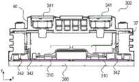
参考图1,示意性地示出了功率半导体模块装置300的截面图。功率半导体模块装置300包括外壳37和半导体衬底310。半导体衬底310包括电介质绝缘层311、附接至电介质绝缘层311的(结构化)第一金属化层3111、以及附接至电介质绝缘层311的(结构化)第二金属化层3112。电介质绝缘层311设置在第一金属化层3111和第二金属化层3112之间。Referring to FIG. 1 , a cross-sectional view of a power
第一金属化层3111和第二金属化层3112中的每者可以由以下材料之一构成或者包括以下材料之一:铜;铜合金;铝;铝合金;在功率半导体模块装置的操作期间保持固态的任何其他金属或合金。半导体衬底310可以是陶瓷衬底,即其中的电介质绝缘层311为陶瓷(例如,薄陶瓷层)的衬底。陶瓷可以由以下材料之一构成或者包括以下材料之一:氧化铝;氮化铝;氧化锆;氮化硅;氮化硼;或者任何其他电介质陶瓷。例如,电介质绝缘层11可以由以下材料之一构成或者包括以下材料之一:Al2O3、AlN、SiC、BeO或Si3N4。例如,衬底310可以是(例如)直接铜键合(DCB)衬底、直接铝键合(DAB)衬底或者活性金属钎焊(AMB)衬底。此外,衬底310可以是绝缘金属衬底(IMS)。例如,绝缘金属衬底一般包括含有诸如环氧树脂或聚酰亚胺的(填充)材料的电介质绝缘层311。例如,电介质绝缘层311的材料可以填充有陶瓷颗粒。这样的颗粒可以包括(例如)Si2O、Al2O3、AlN或BrN,并且可以具有处于大约1μm和大约50μm之间的直径。衬底310也可以是具有非陶瓷电介质绝缘层311的常规印刷电路板(PCB)。例如,非陶瓷电介质绝缘层311可以由固化树脂构成或者包括固化树脂。Each of the
半导体衬底310布置在外壳37中。在图1中所示的示例中,半导体衬底310形成外壳37的底表面,而外壳37本身则唯独包括侧壁和盖。然而,这只是示例。还有可能外壳37还包括底表面,并且半导体衬底310可以布置在外壳37内部。根据另一个示例,半导体衬底310可以安装在基板(图1中未示出)上。在一些功率半导体模块装置300中,多于一个半导体衬底310布置在单个基板(未示出)上。例如,基板可以形成外壳37的底表面。The
一个或多个半导体主体320可以布置在至少一个半导体衬底310上。布置在至少一个半导体衬底310上的半导体主体320中的每者可以包括二极管、IGBT(绝缘栅双极型晶体管)、MOSFET(金属氧化物半导体场效应晶体管)、JFET(结型场效应晶体管)、HEMT(高电子迁移率晶体管)或者任何其他适当的半导体元件。One or
一个或多个半导体主体320可以在半导体衬底310上形成半导体装置。在图1中,仅示例性地示出了两个半导体主体320。图1中的半导体衬底310的第二金属化层3112是连续层。在图1所示的示例中,第一金属化层3111是结构化层。“结构化层”是指第一金属化层3111不是连续层,而是包括处于该层的不同区段之间的凹陷。在图1中示意性地示出了这样的凹陷。这一示例中的第一金属化层3111包括三个不同区段。然而,这只是示例。任何其他数量的区段都是可能的。不同的半导体主体320可以安装至第一金属化层3111的相同区段或不同区段。第一金属化层3111的不同区段可以不具有任何电连接部,或者可以使用(例如)键合引线33电连接至一个或多个其他区段。例如,为了略举几例,电连接部33还可以包括连接板或导体轨。一个或多个半导体主体320可以通过导电连接层330电及机械连接至半导体衬底310。这样的导电连接层可以是焊料层、导电粘合剂层或者烧结的金属粉末(例如,烧结的银粉末)层。One or
根据其他示例,第二金属化层3112也可能是结构化层。还可能省略第二金属化层3112。例如,第一金属化层3111也可能是连续层。According to other examples, the
图1中所示的功率半导体模块装置300还包括端子元件34。端子元件34电连接至第一金属化层3111,并且在外壳37的内部和外部之间提供电连接部。端子元件34可以以第一端电连接至第一金属化层3111,而端子元件34的第二端341从外壳37伸出。可以在端子元件34的第二端341处从外部电接触端子元件34。端子元件34的第一部分可以在垂直方向y上穿过外壳37的内部延伸。垂直方向y是垂直于半导体衬底310的顶表面的方向,其中,半导体衬底310的顶表面是至少一个半导体主体320安装于其上的表面。可以使端子元件34的第二端341弯曲,使得它们在平行于半导体衬底310的顶表面的第一水平方向x上延伸。通过这种方式,可以更易于电接触第二端341。然而,图1所示的端子元件34只是示例。可以通过任何其他方式实施端子元件34,并且可以将端子元件34布置在外壳37内的任何位置。例如,可以将一个或多个端子元件34布置为靠近外壳37的侧壁或者与外壳37的侧壁相邻。端子元件34也可以穿过外壳37的侧壁而不是穿过盖而伸出。第二端341也有可能在垂直方向y上延伸,而非被弯曲到第一水平方向x上。任何其他适当的实施方式都是可能的。The power
半导体主体320均可以包括芯片焊盘金属化部(未具体示出),例如,源极、漏极、阳极、阴极或栅极金属化部。芯片焊盘金属化部一般提供用于电连接半导体主体320的接触表面。例如,芯片焊盘金属化部可以电接触连接层330、端子元件34或电连接部33。例如,芯片焊盘金属化部可以由诸如铝、铜、金或银的金属构成或者包括诸如铝、铜、金或银的金属。例如,电连接部33和端子元件34也可以由诸如铜、铝、金或银的金属构成,或者包括诸如铜、铝、金或银的金属。The
根据一个示例,至少两个半导体主体320可以按照半桥构造进行布置。然而,任何其他布置方式也是可能的。According to one example, the at least two
现在参考图2,示例性地示出了另一个功率半导体模块装置300的截面图。功率半导体模块装置300包括外壳37和基板380。在图2所示的示例中,两个半导体衬底310布置在基板380上。如上文联系图1所描述的,也有可能仅将一个半导体衬底310或者将多于两个半导体衬底310布置在基板380上。功率半导体模块装置300也有可能不包括任何基板380,并且单个衬底310形成外壳37的底部。任何其他适当的实施方式也是可能的。Referring now to FIG. 2 , a cross-sectional view of another power
图2的功率半导体模块装置300还包括用于将一个或多个端子元件34安装至外壳37的安装装置40。根据一个示例,外壳37包括侧壁。安装装置40可以包括框架或主体。该框架或主体可以包括安装部分(图2中未具体示出)。这样的安装部分可以被插入到外壳37的侧壁中的对应的配对部分中。例如,安装部分可以包括销、夹子或钩子,它们可以被插入到外壳37的框架内的对应的配对部分(例如狭槽或孔)中。安装部分可以与对应的配对部分牢固地啮合,从而使得安装装置40牢固地附接至外壳37。在被安装至外壳37时,安装装置40的框架或主体可以形成外壳37的盖的至少一部分。一个或多个端子元件34可以穿过安装装置40延伸。在安装装置40被安装至外壳37时,一个或多个端子元件34中的每者的第二端341可以从外壳37伸出,从而使得可以从外壳37的外部接触第二端341。端子元件34的第一端342从安装装置40伸出到外壳37的内部。端子元件34的第一端342中的每者可以接触第一金属化层3111的各区段之一。例如,第一端342可以被熔接、焊接或者烧结至第一金属化层3111。根据一个示例,第一端342通过超声波熔接而机械及电耦合至第一金属化层3111。The power
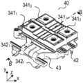
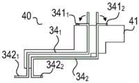
现在参考图3,以三维图示意性地示出了安装装置40。框架或主体41可以具有基本上方形或矩形的形状。然而,框架或主体41可以具有几个突起或凸部。框架或主体41的外形或形状一般取决于外壳37的外形和形状以及端子元件34和安装部分42的外形和形状。Referring now to FIG. 3 , the mounting
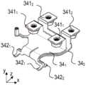
如图3中示例性地示出,安装装置40可以包括框架或主体41以及第一端子元件341和第二端子元件342。第一端子元件341和第二端子元件342可以穿过框架或主体41延伸。端子元件341、342的第一端3421、3422可以在底侧上从框架或主体41伸出,其中,框架或主体41的底侧是在将安装装置40安装至外壳37(图3中未示出外壳37)时面对所述至少一个半导体衬底310的一侧。端子元件341、342的第二端3411、3412在顶侧上从框架或主体41伸出,其中,顶侧布置为与底侧相对,并且在将安装装置40安装至外壳37(图3中未示出外壳37)时,顶侧背离所述至少一个半导体衬底310。中间部分分别在端子元件341、342的第一端3421、3422和第二端3411、3412之间延伸。端子元件341、342的第一端3421、3422和第二端3411、3412与对应的端子元件341、342的中间部分相比可以较短。例如,从框架或主体41伸出的第一端3421、3422可以具有处于0.1cm和1.5cm之间的总长度。例如,从框架或主体41伸出的第二端3411、3412可以具有处于0.1cm和2.0cm之间的总长度。在第一端3421、3422和第二端3411、3412之间延伸的相应的中间部分可以具有处于2.0cm和7.0cm之间的长度。第一端子元件341的中间部分可以通过框架或主体41的材料与第二端子元件342的中间部分介电绝缘。根据一个示例,超过50%、超过60%乃至超过70%的第一端子元件341以及超过50%、超过60%乃至超过70%的第二端子元件342完全被框架或主体41的材料包围。也就是说,框架或主体41的材料使第一端子元件341的主要部分与第二端子元件342的主要部分相互介电绝缘。As exemplarily shown in FIG. 3 , the mounting
第一端3421、3422可以包括可以被安装至第一金属化层3111的(焊接或熔接)脚。例如,第二端3411、3412可以包括连接板。这样的连接板可以包括形成于其中的螺纹孔。通过这种方式,有可能(例如)将外部元件机械及电耦合至连接板。例如,可以通过导电螺栓(图中未示出螺栓)电接触端子元件341、342。这样的导电螺栓可以被插入到螺纹孔中。任何外部元件(未示出)可以通过这样的螺栓机械及电耦合至端子元件341、342。例如,外部元件可以包括连接板、电路板和连接线的至少其中之一。The first ends 3421 , 3422 may include (solder or weld) feet that may be mounted to the
现在参考图4,示意性地示出了没有安装装置40的框架或主体41的第一端子元件341和第二端子元件342。例如,第一端子元件341和第二端子元件342的作为在第一端3421、3422和第二端3411、3412之间延伸的部分的中间部分可以是板状的。然而,图4中所示的第一端子元件341和第二端子元件342的具体外形只是示例。任何其他适当形状也是可能的。第一端子元件341的中间部分可以与第二端子元件342的中间部分基本上平行。第一端子元件341的第一端3421可以朝第一方向弯曲,并且第二端子元件342的第一端3422可以朝与第一方向相反的第二方向弯曲。第一端子元件341的第二端3411也可以朝第一方向弯曲,并且第二端子元件342的第二端3412可以朝与第一方向相反的第二方向弯曲。Referring now to FIG. 4 , the first
在图3和图4所示的示例中,第一端子元件341和第二端子元件342中的每者包括两个第一端3421、3422和两个第二端3411、3412。然而,这只是示例。第一端子元件341和第二端子元件342中的每者可以包括仅一个或者乃至多于两个第一端3421、3422和第二端3411、3412。任何适当的数量的第一端3421、3422和第二端3411、3412都是可能的。第一端3421、3422的数量可以等于或者不同于第二端3411、3412的数量。In the example shown in FIGS. 3 and 4 , each of the first
再次参考图3,框架或主体41可以包括突起43,在将安装装置40安装至外壳37时,突起43从框架或主体41朝所述至少一个半导体衬底310延伸。突起43可以至少部分地包围处于安装装置40的底侧上的中空空间或空腔。至少一个安装元件42可以耦合至突起43。例如,在从顶侧插入到外壳37中时,所述至少一个安装元件42可以与外壳37的对应的配对部分啮合。由安装装置40和突起43限定的中空空间或空腔可以在至少一个水平方向上是开放的,从而允许与环境交换空气。Referring again to FIG. 3 , the frame or
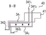
现在参考图5,示例性地示出了安装装置40在截平面B-B’(参见图3)中的截面图。可以看出,在框架或主体41内部,第一端子元件341和第二端子元件342通过框架或主体41的材料相互介电绝缘。可以非常精确地设定第一端子元件341的中间部分和第二端子元件342的中间部分之间的距离d3。第一端子元件341的中间部分和第二端子元件342的中间部分之间的距离d3一般取决于布置在外壳37内的半导体装置的种类以及存在于功率半导体模块装置300中的电压和电流。根据一个示例,例如,第一端子元件341的中间部分和第二端子元件342的中间部分之间的距离d3可以处于1mm和3mm之间,并且特别地为1.5mm。然而,任何其他距离d3也是可能的。框架或主体41的材料一般能够在安装装置40内部的第一端子元件341和第二端子元件342之间提供充分的介电绝缘。Referring now to FIG. 5 , a cross-sectional view of the mounting
可以通过在安装装置40的底侧上形成突起43来延长第一端子元件341和第二端子元件342之间沿安装装置40的外部的爬电距离。在下文中将通过图6对此进行描述。图6示意性地示出了功率半导体模块装置300在截平面A-A’(参见图5)中的截面图。图6的功率半导体模块装置300对应于上文已经联系图1描述的功率半导体模块装置300。然而,包括第一端子元件341和第二端子元件342的安装装置40被插入到外壳37中。在图6的截面图中可以看到第一端子元件341和第二端子元件342的中间部分的截面。框架或主体41的主要部分在图6的截面图中不是直接可见的,因为其布置在所示的图像平面的后面。然而,出于解释目的,在图6中通过虚线示出了框架或主体41的主要部分以及第一端子元件341和第二端子元件342的第二端3411、3412。The creepage distance between the first
在图6中还通过虚线示出了第一端子元件341和第二端子元件342之间沿安装装置40的外部的爬电距离c1。可以看出,爬电距离c1从第一端子元件341沿框架或主体41的顶侧延伸并且进一步沿框架或主体41的侧壁和底侧延伸。突起43延长了爬电距离c1。此外,突起43至少部分地浸入到覆盖半导体衬底310和安装于其上的半导体主体320的包封材料35中。包封材料35进一步降低了任何爬电电流,因为其阻挡了穿过自由空气的直接路径。通过提供突起43,有可能使包封材料35的厚度d2保持相对较低。在没有所述突起的情况下,包封材料35的厚度将必须显著更高(至少达到部分地包封框架或主体41的高度),以便能够降低爬电电流。因此,通过提供突起43,与其他功率半导体模块装置300相比,可以降低包封材料35的量。包封材料35的降低的厚度d2可以进一步导致降低功率半导体模块装置300内部的张力和应力。The creepage distance c1 along the outside of the mounting
例如,包封材料35可以包括硅酮凝胶,或者可以是刚性模制化合物。普遍用作包封材料35或浇注化合物的材料往往具有显著不同于功率半导体模块装置300的其他元件(例如,半导体衬底310或半导体主体320)的热膨胀系数CTE的CTE。在两种具有(显著)不同的CTE的材料之间的界面处,可能出现张力或应力。如果包封材料35具有大的厚度d2,那么可能进一步提高这样的张力或应力。因此,通过降低包封材料35的厚度d2,可以降低功率半导体模块装置300内部的张力或应力。For example, the
现在参考图7,示例性地示出了用于制作安装装置40的方法。参考图7A,可以将第一端子元件341注入到安装装置40的框架或主体41中。例如,框架或主体41可以是通过注塑模制形成的。可以将框架或主体41的材料注入到注塑模具(图7A中未具体示出)中。第一端子元件341可以布置到注塑模具内,从而使得在将所述材料注入到注塑模具中时,第一端子元件341被注入到所述材料中。随后可以进行硬化步骤(未示出)。注塑模具可以具有一定形状,使得框架或主体41的某些部分保持没有所述材料,并且在框架或主体41中保留中空空间。之后,可以将第二端子元件342插入(例如,推入或滑入)到这些中空空间中。这在图7B种示例性地示出,其中,将第二端子元件342从底侧插入到框架或主体41中。然而,这只是示例。如果相应地在框架或主体41内部形成了中空空间,那么也有可能从侧面将第二端子元件342滑入到框架或主体41中。图7C示意性地示出了插入第二端子元件342之后的安装装置40。因此,可以通过首先将第一端子元件341注入到框架或主体41中,并且然后将第二端子元件342插入(或者推入或滑入)到框架或主体41的中空空间中来形成安装装置40。所述中空空间可以具有对应于第二端子元件342的外形和尺寸的外形和尺寸。Referring now to FIG. 7 , a method for making the mounting
如图7A到图7C中示意性地示出,端子元件341、342的第二端3411、3412可以在垂直方向y上从安装装置40伸出。起初第二端3411、3412可以垂直于半导体衬底310的顶表面。然而,如图7D中所示,第二端3411、3412可以弯曲基本上90°。也就是说,当将安装装置40安装至外壳37时,在最终位置处,第二端3411、3412可以平行于半导体衬底310的顶表面延伸。As schematically shown in FIGS. 7A to 7C , the second ends 3411 , 3412 of the
例如,在将第二端子元件342插入到框架或主体41中之后,可以同时将第二端3411、3412从安装位置弯曲到最终位置。然而,这只是示例。根据另一个示例,在将第一端子元件341注入到框架或主体41中之后并且在将第二端子元件342插入到框架或主体41中之前,可以将第一端子元件341的第二端3411从安装位置直接弯曲到最终位置。在稍后阶段,即,在将第二端子元件342插入到框架或主体41中之后,可以将第二端子元件342的第二端3412从安装位置弯曲到最终位置。For example, after inserting thesecond
根据另一个示例,可以在将第二端3411、3412从其安装位置弯曲到其最终位置之前,将一个或多个螺母(未示出)布置在框架或主体41上或者框架或主体41内的中空空间内。当第二端3411、3412处于其从平行于半导体衬底310的顶表面延伸的最终位置时,可以将一个螺母布置在第二端3411、3412中的每者下方(处于框架或主体41与对应的第二端3411、3412之间)。通过这种方式,可以更容易地将螺栓插入到框架或主体41中,并且螺栓可以与螺母和对应的第二端3411、3412牢固地啮合。According to another example, one or more nuts (not shown) may be arranged on the frame or
在下文中,将描述几种示例性功率半导体模块装置、安装装置和方法。In the following, several exemplary power semiconductor module arrangements, mounting arrangements and methods will be described.
1.示例:一种功率半导体模块装置300包括:布置在外壳37中的半导体衬底310,其中,至少一个半导体主体320布置在半导体衬底310上。所述功率半导体模块装置还包括具有框架或主体41、第一端子元件341和第二端子元件342的安装装置40。安装装置40被插入到外壳37中并与外壳37耦合,第一端子元件341和第二端子元件342中的每者以第一端3421、3422机械及电接触半导体衬底310,第一端子元件341和第二端子元件342中的每者的中间部分穿过框架或主体41延伸,第一端子元件341和第二端子元件342中的每者的第二端3411、3412延伸到所述外壳37外部,并且第一端子元件341通过框架或主体41的部分与所述第二端子元件342介电绝缘。第一端子元件341被注入到框架或主体41中并且与框架或主体41不可分开地耦合,并且所述第二端子元件342布置在框架或主体41内部的中空空间内,并且与框架或主体41可拆分地耦合。1. Example: A power
2.示例:根据示例1所述的功率半导体模块装置300,还包括处于外壳37内部的浇注材料35,浇注材料35覆盖半导体衬底310和安装于其上的至少一个半导体主体320。2. Example: The power
3.示例:根据示例1或2所述的功率半导体模块装置300,其中,安装装置40还包括突起43,在安装装置40被插入到外壳37中并与外壳37耦合时,突起43从框架或主体41朝至少一个半导体衬底310延伸。3. Example: The power
4.示例:根据示例3所述的功率半导体模块装置300,其中,突起43部分地浸入到浇注材料35中,并且在浇注材料35和安装装置40之间限定中空空间。4. Example: The power
5.示例:根据示例4所述的功率半导体模块装置300,其中,所述中空空间在一个水平方向上是开放的。5. Example: The power
6.示例:根据前述示例中的任何一项所述的功率半导体模块装置300,其中,在框架或主体41内部的第一端子元件341和第二端子元件342之间的距离d3处于1mm和3mm之间。6. Example: The power
7.示例:根据示例6所述的功率半导体模块装置300,其中,在框架或主体41内部的第一端子元件341和第二端子元件342之间的距离d3为1.5mm。7. Example: The power
8.示例:根据前述示例中的任何一项所述的功率半导体模块装置300,其中,在安装装置40被插入到外壳37中并与外壳37耦合时,第二端3411、3412中的每者在外壳37外部并且平行于半导体衬底310的顶表面延伸,其中,半导体衬底310的顶表面是至少一个半导体主体320安装于其上的表面。8. Example:The power
9.示例:根据前述示例中的任何一项所述的功率半导体模块装置300,其中,安装装置40形成外壳37的盖的至少一部分。9. Example: The power
10.示例:一种安装装置40包括:框架或主体41、第一端子元件341和第二端子元件342,其中,安装装置40被配置为插入在功率半导体模块装置300的所述外壳37中并与外壳37耦合,功率半导体模块装置300包括布置在外壳37中的半导体衬底310,其中,至少一个半导体主体320布置在所述半导体衬底310上。在所述安装装置40被插入到外壳37中并与外壳耦合时,所述第一端子元件和所述第二端子元件341、342中的每者被配置为以第一端3421、3422机械及电接触半导体衬底310。第一端子元件341和第二端子元件342中的每者的中间部分通过该框架或主体41延伸,第一端子元件341和第二端子元件342中的每者的第二端3411、3412延伸到外壳37外部,并且第一端子元件341通过框架或主体41的部分与第二端子元件342介电绝缘。第一端子元件341被注入到框架或主体41中并且与框架或主体41不可分开地耦合,并且所述第二端子元件342布置到框架或主体41内部的中空空间内,并且与框架或主体41可拆分地耦合。10. Example: A mounting
11.示例:一种方法包括:将第一材料注入到注塑模具中,由此形成安装装置40的框架或主体41,其中,第一端子元件341布置在注塑模具中,并且被注入到第一材料中,并且其中,在框架或主体41中形成没有第一材料的至少一个中空空间。所述方法还包括使第一材料硬化,并且将第二端子元件342插入到框架或主体41的所述至少一个中空空间之一中。11. Example: A method comprising: injecting a first material into an injection mold, thereby forming the frame or
12.示例:根据示例11所述的方法,还包括将具有布置于其中的第一端子元件341和第二端子元件342的框架或主体41安装至功率半导体模块装置300的外壳37,其中,功率半导体模块装置300包括布置于外壳37内部的半导体衬底310,半导体衬底310具有安装于其上的至少一个半导体主体320。在将具有布置于其中的第一端子元件341和第二端子元件342的框架或主体41安装至外壳37时,第一端子元件341的第一端3421和第二端子元件342的第一端3422机械及电接触半导体衬底310。12. Example: The method of example 11, further comprising mounting the frame or
13.示例:根据示例12所述的方法,还包括通过超声波熔接在第一端子元件341的第一端3421与半导体衬底310之间以及在第二端子元件342的第一端3422与半导体衬底310之间形成机械及电接头。13. Example: The method of Example 12, further comprising ultrasonically welding between the
14.示例:根据示例11到13中的任何一项所述的方法,其中,形成框架或主体41包括形成突起43,在将具有布置于其中的第一端子元件341和第二端子元件342的框架或主体41安装至外壳37时,突起43从框架或主体41朝半导体衬底310延伸,所述方法还包括将浇注材料35填充到外壳37中,使得浇注材料35覆盖半导体衬底310以及安装于其上的至少一个半导体主体320,并且突起43部分地浸入到浇注材料35中。14. Example: The method of any one of examples 11 to 13, wherein forming the frame or
Claims (14)
Translated fromChineseApplications Claiming Priority (2)
| Application Number | Priority Date | Filing Date | Title |
|---|---|---|---|
| EP19172724.7AEP3736855A1 (en) | 2019-05-06 | 2019-05-06 | Power semiconductor module arrangement and method for producing the same |
| EP19172724.7 | 2019-05-06 |
Publications (1)
| Publication Number | Publication Date |
|---|---|
| CN111900134Atrue CN111900134A (en) | 2020-11-06 |
Family
ID=66439889
Family Applications (1)
| Application Number | Title | Priority Date | Filing Date |
|---|---|---|---|
| CN202010362239.9APendingCN111900134A (en) | 2019-05-06 | 2020-04-30 | Power semiconductor module device and method of manufacturing the same |
Country Status (3)
| Country | Link |
|---|---|
| US (2) | US11462446B2 (en) |
| EP (1) | EP3736855A1 (en) |
| CN (1) | CN111900134A (en) |
Cited By (1)
| Publication number | Priority date | Publication date | Assignee | Title |
|---|---|---|---|---|
| US20220359365A1 (en)* | 2017-12-15 | 2022-11-10 | Infineon Technologies Ag | Power semiconductor module arrangement |
Families Citing this family (3)
| Publication number | Priority date | Publication date | Assignee | Title |
|---|---|---|---|---|
| EP4195254A1 (en) | 2021-12-10 | 2023-06-14 | Infineon Technologies AG | Housing, semiconductor module comprising a housing and method for producing a housing |
| EP4220704A1 (en)* | 2022-01-27 | 2023-08-02 | Infineon Technologies AG | Printed circuit board, power semiconductor module arrangement comprising a printed circuit board, and method for assembling the same |
| EP4601424A1 (en)* | 2024-02-06 | 2025-08-13 | Infineon Technologies AG | Power semiconductor module arrangement |
Citations (6)
| Publication number | Priority date | Publication date | Assignee | Title |
|---|---|---|---|---|
| US5751058A (en)* | 1995-10-25 | 1998-05-12 | Mitsubishi Denki Kabushiki Kaisha | Semiconductor device having parallel overlapping main current terminals |
| JP2003068979A (en)* | 2001-08-28 | 2003-03-07 | Hitachi Ltd | Semiconductor device |
| US20070187817A1 (en)* | 2006-02-13 | 2007-08-16 | Semikron Elektronik Gmbh & Co. Kg | Power semiconductor modules and method for producing them |
| US20130056883A1 (en)* | 2011-09-01 | 2013-03-07 | Kabushiki Kaisha Toshiba | Semiconductor device and method of manufacturing the same |
| US20130277819A1 (en)* | 2012-04-20 | 2013-10-24 | Hiroshi Yoshida | Semiconductor device and method of manufacturing semiconductor device |
| US20160254255A1 (en)* | 2014-05-15 | 2016-09-01 | Fuji Electric Co., Ltd. | Power semiconductor module and composite module |
Family Cites Families (9)
| Publication number | Priority date | Publication date | Assignee | Title |
|---|---|---|---|---|
| US8018047B2 (en) | 2007-08-06 | 2011-09-13 | Infineon Technologies Ag | Power semiconductor module including a multilayer substrate |
| JP5272768B2 (en) | 2009-02-05 | 2013-08-28 | 三菱電機株式会社 | Power semiconductor device and manufacturing method thereof |
| JP5211364B2 (en) | 2010-05-07 | 2013-06-12 | 三菱電機株式会社 | Semiconductor device |
| JP5656907B2 (en)* | 2012-04-11 | 2015-01-21 | 三菱電機株式会社 | Power module |
| WO2015176985A1 (en) | 2014-05-20 | 2015-11-26 | Abb Technology Ag | Semiconductor power module with low stray inductance |
| DE102014115847B4 (en) | 2014-10-30 | 2018-03-08 | Infineon Technologies Ag | Method for producing a power semiconductor module |
| JP6591808B2 (en) | 2015-07-06 | 2019-10-16 | ローム株式会社 | Power module and inverter device |
| US9443792B1 (en) | 2015-10-31 | 2016-09-13 | Ixys Corporation | Bridging DMB structure for wire bonding in a power semiconductor device module |
| JP7162013B2 (en)* | 2017-05-02 | 2022-10-27 | ヒタチ・エナジー・スウィツァーランド・アクチェンゲゼルシャフト | Half-bridge module with coaxial array of DC terminals |
- 2019
- 2019-05-06EPEP19172724.7Apatent/EP3736855A1/enactivePending
- 2020
- 2020-04-30CNCN202010362239.9Apatent/CN111900134A/enactivePending
- 2020-05-05USUS16/866,990patent/US11462446B2/enactiveActive
- 2022
- 2022-07-25USUS17/872,436patent/US11699625B2/enactiveActive
Patent Citations (6)
| Publication number | Priority date | Publication date | Assignee | Title |
|---|---|---|---|---|
| US5751058A (en)* | 1995-10-25 | 1998-05-12 | Mitsubishi Denki Kabushiki Kaisha | Semiconductor device having parallel overlapping main current terminals |
| JP2003068979A (en)* | 2001-08-28 | 2003-03-07 | Hitachi Ltd | Semiconductor device |
| US20070187817A1 (en)* | 2006-02-13 | 2007-08-16 | Semikron Elektronik Gmbh & Co. Kg | Power semiconductor modules and method for producing them |
| US20130056883A1 (en)* | 2011-09-01 | 2013-03-07 | Kabushiki Kaisha Toshiba | Semiconductor device and method of manufacturing the same |
| US20130277819A1 (en)* | 2012-04-20 | 2013-10-24 | Hiroshi Yoshida | Semiconductor device and method of manufacturing semiconductor device |
| US20160254255A1 (en)* | 2014-05-15 | 2016-09-01 | Fuji Electric Co., Ltd. | Power semiconductor module and composite module |
Cited By (2)
| Publication number | Priority date | Publication date | Assignee | Title |
|---|---|---|---|---|
| US20220359365A1 (en)* | 2017-12-15 | 2022-11-10 | Infineon Technologies Ag | Power semiconductor module arrangement |
| US11978700B2 (en)* | 2017-12-15 | 2024-05-07 | Infineon Technologies Ag | Power semiconductor module arrangement |
Also Published As
| Publication number | Publication date |
|---|---|
| US11699625B2 (en) | 2023-07-11 |
| US11462446B2 (en) | 2022-10-04 |
| EP3736855A1 (en) | 2020-11-11 |
| US20220359319A1 (en) | 2022-11-10 |
| US20200357710A1 (en) | 2020-11-12 |
Similar Documents
| Publication | Publication Date | Title |
|---|---|---|
| CN109935574B (en) | Semiconductor module and method for producing semiconductor module | |
| US11699625B2 (en) | Power semiconductor module arrangement | |
| CN113690192B (en) | Power semiconductor module and method for manufacturing a power semiconductor module | |
| CN113903727A (en) | Power semiconductor module and method for manufacturing a power semiconductor module | |
| US20230170287A1 (en) | Power semiconductor module, method for assembling a power semiconductor module and housing for a power semiconductor module | |
| CN110047761A (en) | Semiconductor module and its manufacturing method | |
| CN105027276B (en) | Semiconductor device | |
| EP3859775A1 (en) | Semiconductor arrangement and method for producing the same | |
| US12387987B2 (en) | Housing, semiconductor module comprising a housing and method for producing a housing | |
| CN110931437A (en) | Power semiconductor module arrangement and housing for a power semiconductor module arrangement | |
| EP4084062A1 (en) | Power semiconductor module arrangement | |
| US11282774B2 (en) | Power semiconductor module arrangement | |
| CN111900135B (en) | Power semiconductor module device | |
| US20230343681A1 (en) | Power Semiconductor Module Arrangements and Methods for Producing Power Semiconductor Module Arrangements | |
| US12261063B2 (en) | Method and device for producing a housing | |
| EP4148789A1 (en) | Power semiconductor modules | |
| US20250273520A1 (en) | Housing, semiconductor module having a housing, and method for assembling a semiconductor module | |
| EP4604176A1 (en) | Semiconductor module arrangement, electronics carrier for a semiconductor module arrangement, and method for producing a semiconductor module arrangement | |
| EP4050650A1 (en) | Power semiconductor module arrangement | |
| CN117038476A (en) | Method for producing a power semiconductor module | |
| EP3951866A1 (en) | Semiconductor substrate arrangement and method for producing the same | |
| CN116507018A (en) | Printed circuit board, arrangement of power semiconductor modules including printed circuit board and method for assembling the same |
Legal Events
| Date | Code | Title | Description |
|---|---|---|---|
| PB01 | Publication | ||
| PB01 | Publication | ||
| SE01 | Entry into force of request for substantive examination | ||
| SE01 | Entry into force of request for substantive examination |